US6226723B1 - Bifurcated data and command/address communication bus architecture for random access memories employing synchronous communication protocols - Google Patents
Bifurcated data and command/address communication bus architecture for random access memories employing synchronous communication protocols Download PDFInfo
- Publication number
- US6226723B1 US6226723B1 US08/909,299 US90929997A US6226723B1 US 6226723 B1 US6226723 B1 US 6226723B1 US 90929997 A US90929997 A US 90929997A US 6226723 B1 US6226723 B1 US 6226723B1
- Authority
- US
- United States
- Prior art keywords
- data
- controller
- memory modules
- memory
- information
- Prior art date
- Legal status (The legal status is an assumption and is not a legal conclusion. Google has not performed a legal analysis and makes no representation as to the accuracy of the status listed.)
- Expired - Fee Related
Links
Images


Classifications
-
- G—PHYSICS
- G11—INFORMATION STORAGE
- G11C—STATIC STORES
- G11C7/00—Arrangements for writing information into, or reading information out from, a digital store
- G11C7/10—Input/output [I/O] data interface arrangements, e.g. I/O data control circuits, I/O data buffers
- G11C7/1078—Data input circuits, e.g. write amplifiers, data input buffers, data input registers, data input level conversion circuits
- G11C7/109—Control signal input circuits
-
- G—PHYSICS
- G11—INFORMATION STORAGE
- G11C—STATIC STORES
- G11C7/00—Arrangements for writing information into, or reading information out from, a digital store
- G11C7/10—Input/output [I/O] data interface arrangements, e.g. I/O data control circuits, I/O data buffers
-
- G—PHYSICS
- G11—INFORMATION STORAGE
- G11C—STATIC STORES
- G11C7/00—Arrangements for writing information into, or reading information out from, a digital store
- G11C7/10—Input/output [I/O] data interface arrangements, e.g. I/O data control circuits, I/O data buffers
- G11C7/1051—Data output circuits, e.g. read-out amplifiers, data output buffers, data output registers, data output level conversion circuits
- G11C7/1057—Data output buffers, e.g. comprising level conversion circuits, circuits for adapting load
-
- G—PHYSICS
- G11—INFORMATION STORAGE
- G11C—STATIC STORES
- G11C7/00—Arrangements for writing information into, or reading information out from, a digital store
- G11C7/10—Input/output [I/O] data interface arrangements, e.g. I/O data control circuits, I/O data buffers
- G11C7/1051—Data output circuits, e.g. read-out amplifiers, data output buffers, data output registers, data output level conversion circuits
- G11C7/106—Data output latches
-
- G—PHYSICS
- G11—INFORMATION STORAGE
- G11C—STATIC STORES
- G11C7/00—Arrangements for writing information into, or reading information out from, a digital store
- G11C7/10—Input/output [I/O] data interface arrangements, e.g. I/O data control circuits, I/O data buffers
- G11C7/1072—Input/output [I/O] data interface arrangements, e.g. I/O data control circuits, I/O data buffers for memories with random access ports synchronised on clock signal pulse trains, e.g. synchronous memories, self timed memories
-
- G—PHYSICS
- G11—INFORMATION STORAGE
- G11C—STATIC STORES
- G11C7/00—Arrangements for writing information into, or reading information out from, a digital store
- G11C7/10—Input/output [I/O] data interface arrangements, e.g. I/O data control circuits, I/O data buffers
- G11C7/1078—Data input circuits, e.g. write amplifiers, data input buffers, data input registers, data input level conversion circuits
- G11C7/1087—Data input latches
Definitions
- a Paper Appendix of an IEEE draft standard P1596.7-199X including an embodiment of the invention comprising sixty-seven sheets is included herewith and incorporated by reference in its entirety for all purposes.
- the present invention relates to computer memories. More particularly, the present invention pertains to an improved memory interface particularly useful for dynamic random access memories and communication protocols therefor.
- DRAM dynamic random access memory
- FIG. 1 digital information, or data, is stored in an arrangement of memory cells 3 , configured in a matrix of intersecting rows 5 and columns 6 .
- the rows 5 may be referred to as word lines 5 .
- Each memory cell comprises a storage capacitor (not shown) capable of holding a charge and a metal-oxide semiconductor field effect transistor (MOSFET) (not shown) for accessing the capacitor charge; hereinafter this transistor is referred to as an access transistor.
- MOSFET metal-oxide semiconductor field effect transistor
- the charge is a voltage potential referred to as a data bit and is typified as either a high voltage or a low voltage. Therefore, the memory has two states, often thought of as the true logic state and the complementary logic state.
- the data bit is amplified and latched to the digit lines 7 by a sense amplifier 8 .
- a bit of data may be stored in a specific cell in the write mode, or a bit of data may be retrieved from a specific cell in the read mode.
- the data is either transferred from the digit lines 7 to Input/Output lines (I/O) 9 in the read mode; or transferred from the I/O lines 9 to the digit lines 7 in the write mode. In either case, the data is transferred through MOSFETs 10 used as switching devices and called decode transistors. For each bit of data stored, its true logic state is available at a first I/O line 11 and its complementary logic state is available at a second I/O line 13 , designated I/O complement.
- I/O and I/O complement lines are often referred to as just I/O lines 9 .
- each cell 3 is only connected to one digit line 7 through an activated access transistor, each cell 3 is electrically referenced to two digit lines 7 , referred to as a digit line pair 15 , through the sense amplifiers 8 .
- the digit line pair 15 comprises the “digit line” 17 for coupling true data and the “digit bar line” 19 for coupling complementary data.
- the digit line 17 is referred to as digit and the digit bar line 19 is referred to as digit bar.
- the digit line pair 15 couples the true and complementary data between the selected cell 3 and the I/O lines.
- a row 5 of cells 3 is selected and connected to the sense amplifier 8 when the row decoder 21 activates the word line 5 .
- the column decoder 23 connects a subset of the sense amplifiers 8 to the I/O lines of the memory.
- Prior art attempts to enhance the performance of a DRAM memory has involved routing control and data information on differing bus architectures.
- One attempt involves transmitting read and write data over separate data lines, typically referred to as a separated I/O type of semiconductor memory. Examples of a separated I/O memory as disclosed in U.S. Pat. No. 5,323,349 to Hamade et al., U.S. Pat. No. 5,307,314 to Lee, and U.S. Pat. No. 4,954,992 to Kumanoya et al.
- separated I/O memory is typically employed on a dynamic random access memory (DRAM).
- DRAM dynamic random access memory
- control and address information are on communication lines which are separate from the data lines.
- a variation of the previously described separated I/O memory involves using a common uni-directional bus for control and data information transmitted to the DRAM.
- a second uni-directional bus is employed to transmit data information coming from the DRAM. This provides good performance for a relatively uniform mix of read and writes, but performance degrades rapidly for long sequences of either reading or writing data, which occurs commonly.
- One of the busses is substantially underutilized, resulting in a reduction in throughput.
- Another attempt at enhancing the performance of a DRAM involves having a bi-directional bus on which all the data information and control information are transmitted. This requires time multiplexing the transmission of the control information, the address information and the data, reducing the effective throughput of the device well below the bandwidth limit of the bus and increasing the power consumed to effectuate data transfers.
- a computer memory device features a high-bandwidth memory interface to transfer information between a controller and the memory cells of a memory module.
- Bifurcated communication busses are provided to take advantage of the memory interface.
- One of the busses, dataLink is dedicated to data information transfer, between the controller and the memory modules, with the remaining bus, commandLink, being dedicated to command/address information transfer therebetween. This facilitates communication between the controller and the memory modules using information packets, bifurcated into data packets and command/address packets.
- the interface circuitry includes encoded chip select techniques that employs slaveId comparison logic, a plurality of control registers and delay registers to regulate the synchronization of communication transfers over the commandLink and the dataLink, as well as a queue register in which the packets are temporarily stored.
- the packets are scheduled to be placed on the appropriate busses so as to maximize data transfer, while minimizing power consumption of the memory device. Synchronization of the communication transfers on the commandLink and the dataLink is achieved during initialization of the memory device and may be periodically checked during normal operations, without degrading transfer throughput. In this fashion, the memory device may be easily scaled so that variable bandwidth data transfers may be provided while maximizing the quantity of data transferred on the dataLink and reducing the power necessary to achieve the same.
- the computer memory device includes an array of memory modules.
- Each of the memory modules includes a matrix of memory cells and a plurality of data transfer ports, a plurality of control transfer ports, with the high-bandwidth memory interface coupled between the matrix of memory cells and the plurality of data and control transfer ports.
- the data transfer ports may be separate input/output ports or a port which handles both data input and data output.
- the controller has a system input port for receiving information from a central processing unit, CPU, and a plurality of data output ports, as well as a plurality of control/address output ports.
- the data output ports and the control/address output ports are in signal communication with the array of memory modules via the dataLink and the commandLink, respectively.
- the dataLink is coupled between the data transfer ports and the data output ports
- the commandLink is coupled between control transfer ports and the control output ports.
- the commandLink is connected so that one of the plurality of control transfer ports of each of the memory modules is connected in common to receive, concurrently, the chip select coding information.
- the array of memory modules may consist of a 1 ⁇ 1 array of dynamic random access memory integrated circuits.
- the array may, however, include a plurality of columns of memory module, with each column having a dataLink which is electrically isolated from the dataLink associated with the remaining columns of memory modules. Configuring the dataLinks in this fashion may result in command/address signals propagating over the commandLink over a distance differing from the distance over which the data signals propagate over the dataLink.
- the controller is adapted to produce packets of information implementing synchronization protocols to adjust the transfer time of information over both the dataLink and the commandLink.
- the controller implements a protocol to vary the power level of the memory device to an intermediate level, standbyMode. In the standbyMode, the power consumption of the memory device is greatly reduced without substantially sacrificing response time to information transmitted over the commandLink or the dataLink.
- FIG. 1 is a block diagram of a prior art computer memory device disclosed in FIG. 1 of U.S. Pat. No. 5,307,314;
- FIG. 2 is a block diagram of a computer memory device in accord with the present invention.
- FIG. 3 is a block diagram of an alternate embodiment of the computer memory device shown in FIG. 2 including multiple columns of memory modules;
- FIG. 4 is a block diagram of an alternate embodiment of the computer memory device shown in FIG. 2 including multiple columns and multiple rows of memory modules;
- FIG. 5 is a detailed block diagram showing the high-bandwidth interface of a memory module, shown in FIG. 2;
- FIG. 6 is a schematic view showing a data packet employed to transfer data information between a controller and memory modules, shown in FIG. 1;
- FIG. 7 is a schematic view showing a request packet employed to communicate control and address information between a controller and memory modules, shown in FIG. 1;
- FIG. 8 is a schematic view showing an information packet associated with a Sync protocol employed to adjust the transfer rate of control and address information between a controller and memory modules, shown in FIG. 1;
- FIG. 9 is a schematic view showing an information packet associated with a Store protocol employed to facilitate communication of control information between a controller and memory modules, shown in FIG. 1;
- FIG. 10 is a schematic view showing an information packet associated with a Load protocol employed to facilitate a controller reading status information in the memory modules, shown in FIG. 1;
- FIG. 11 is a schematic view showing an information packet associated with a write Sync protocol employed to adjust the transfer rate of data information between a controller and memory modules, shown in FIG. 1;
- FIG. 12 is a timing diagram showing synchronization of various control signals of the memory device, shown in FIG. 1, when entering an intermediate power level;
- FIG. 13 is a timing diagram showing synchronization of various control signals of the memory device, shown in FIG. 1, when entering an intermediate power level;
- FIG. 14 is a timing diagram showing synchronization of various control signals of the memory device, shown in FIG. 1, when recovering from an intermediate power level.
- the memory device 30 that may be employed in a personal computer (not shown) or workstation (not shown), includes an array 32 of memory modules 34 , such as a dynamic random access memory integrated circuit (DRAM), coupled to a controller 36 via bifurcated communication busses 38 and 40 .
- Communication bus 38 is dedicated to data information transfer, referred to as dataLink, between the controller 36 and the memory modules 34
- communication bus 40 referred to as commandLink
- the conmandLink 40 is unidirectional, and the dataLink 38 is bi-directional.
- each memory module 34 includes a plurality of data transfer ports 42 and a plurality of control transfer ports 44 .
- the controller 36 has a system input port 46 , for receiving information from a central processing unit (not shown), as well as a plurality of data output ports 48 and a plurality of control/address output ports 49 .
- the data output ports 48 and the control/address output ports 49 are in data communication with the array 32 of memory modules 34 via the dataLink 38 and the commandLink 40 , respectively.
- the commandLink 40 is coupled to the array 32 so that one of the plurality of control transfer ports of each of the memory modules 34 is connected in common to receive, concurrently, control/address signals.
- any signals may be employed on both the dataLink 38 and the commandLink 40 , it is preferred to use signals associated with high performance, low-voltage-swing technology, such as JEDEC SSTL-3 signals.
- Any width bus may be employed to form the commandLink 40 and the dataLink 38 , depending upon the application.
- the dataLink 38 width is chosen so as to compromise between the cost of pins, bonding pads, board area, and the bandwidth required for each memory module 34 .
- the width of the dataLink 38 is a multiple of eight, so that the byte addresses map trivially to the data position thereon.
- the width of the commandLink 40 is selected so that the command/address information transmitted thereon takes no longer time to propagate between the memory modules and the controller 36 than the time required for the corresponding data information to propagate on the dataLink 38 . In this fashion, a sufficient quantity of command/address information may be transmitted over the commandLink 40 to maximize transmission of data information over the dataLink 38 .
- a ten bit wide bus is employed for the commandLink 40
- a sixteen bit wide bus is employed for the dataLink 38 .
- An advantage with employing the aforementioned bifurcated communication busses 38 and 40 is that the data bandwidth of the memory system 30 may be easily scaled up or scaled down. Specifically, as shown in FIG. 3, with the commandLink 40 connected in common with all of the memory modules 34 , the data bandwidth of memory system 130 may be easily increased by having each memory module 34 uniquely associated with a separate dataLink 38 a , 3 b , 38 c and 38 d . In this fashion, a one-row multiple-column, 1 ⁇ N, array 132 of memory modules 34 is formed increasing the data throughput over the system 30 shown in FIG. 2 . For example, transferring a sixty-four byte data burst, on the system 30 shown in FIG. 2, would require the controller 36 to request eight bursts of data be transferred over the dataLink 40 . This results in two bytes being transferred during a given unit of time for a total of eight bytes being transferred per burst.
- the higher performance system shown in FIG. 3, having four separate dataLinks, 38 a , 38 b , 38 c and 38 d , requires only two bursts of data to achieve a transfer of a sixty-four byte data burst.
- the performance of a memory device depends upon the number and capacities of the memory modules 34 , as well as the number of dataLinks 38 routed thereto. Further flexibility may be obtained by increasing the number of rows of memory modules 34 , providing a memory system 230 having an N ⁇ M array 232 of memory modules 34 , shown in FIG. 4 .
- each memory module 34 includes a high-bandwidth memory interface 60 to synchronize transfer of command/address information and data information over the commandLink 40 and the dataLink 38 with the remaining memory modules 34 .
- the high-bandwidth memory interface 60 is coupled between a matrix 61 of memory cells 63 and the data and control transfer ports.
- the memory cells 63 may be coupled to a sense amplifier 65 , as discussed above with respect to FIG. 1 .
- the memory interface 60 includes slaveId comparison logic 62 , a plurality of control registers 64 , 66 and 68 , and delay registers 74 , 76 and 78 .
- the slaveId logic 62 includes a slaveId register 80 and a comparison register 82 .
- slaveId logic 62 takes advantage of encoded chip select techniques to allow the controller to distinguish between the various memory modules 34 of the array 32 by storing information in the slaveId register 80 which differs from the information in the slaveId registers 80 of the remaining memory modules 34 of the array 32 . This allows concurrently transmitting, over the commandLink 40 , command/address information to different subsets of multiple memory modules 34 and receiving data information over the dataLink 38 , discussed more fully below.
- Scaling the dataLink 38 may result in command/address information propagating over the commandLink 40 a distance differing from the distance over which the data information propagate over the dataLink 38 .
- the delay registers 74 , 76 and 78 of the interface logic 60 are established, upon initialization of the memory device 30 , to reduce any delay in the transmission of information on the dataLink and the commandLink.
- An additional advantage is provided in that memory modules 34 having differing access speeds may be employed in the same array 32 , because the delay register 74 , 76 and 78 may be adjusted to synchronize communication transfers over the commandLink 40 and the dataLink 38 by the different memory modules 34 . Typically, the memory modules 34 would be set to transfer data at the speed of the slowest attached memory module 34 . A more exacting synchronization protocol is discussed more fully below.
- the scheduling of the aforementioned transfers may be simplified to allow the use of commands to achieve multiples data burst, which save power by leaving the commandLink 40 idle at times during multiple data transfers.
- communication between the controller 36 and the array 32 of memory modules 36 is scheduled by the controller 36 's transmission of packetized information over the dataLink 38 and the commandLink 40 , shown in FIG. 1 .
- the packets of information on the dataLink 38 contain only data information and need no address or other header information.
- the format of the data packet 90 transferred over the wide dataLink 38 shown in FIG. 6, includes sixteen bits of data.
- the one bit fields 92 are optional and typically correspond to the implementation of Error Correcting Codes associated with eighteen bit memory modules.
- request packets 94 transferred on the commandLink 40 , commence with a zero-to-one flag value transition.
- the request packets 94 may be of either a read or write request, with the flag maintaining the one value for one bit time, and then returns to zero, maintaining that value until a subsequent request packet 84 arrives.
- the first seven bits 96 within the request packets 94 define the slaveId value in the range of zero to sixty-three.
- the slaveId values that exceed the sixty-three value are reserved for special addressing schemes of the memory modules 34 , such as broadcast, multicast, and directed packets, as shown in Table 1.
- the request packets 94 also carry information specifying whether to take advantage of faster timing by accessing an already-open row, and whether to leave the row open or not, indicating whether a burst size of four, eight or sixteen bit bursts shall occur, per clock cycle, as well as determining whether to use the even or the odd dataclock signal for timing.
- the longer bursts may permit saving power by not driving the commandLink 40 unnecessarily. They are also convenient sizes for common cache-line bursts and common configurations.
- the command and subcommand bits in the second and third fields of the request packet 94 provide command protocols for controlling the memory interface 60 . This provides greater flexibility in regulating the timing and transmission of data packets 90 and request packets 94 format and general function, as shown in Table 2. Several specific command protocols for request packets are defined in the following sections.
- an open row corresponds to a row of memory cells within a memory module that already has the data associated therewith stored in the sense amplifier
- a closed row is a row for which the sense amplifier is not storing data.
- Size denotes the number of bits to be transferred
- R/W corresponds to whether the data transfer consists of a read operation of a memory cell or a write operation thereto.
- LeaveRow corresponds to the state at which the row which was the subject of a read or write operation is to be left with the data transferred thereto in the sense amplifier or the addressed memory cell.
- the data clock refers to whether the protocol is to occur on an even or odd clock cycle.
- the packets of information, indicated in Table 2 as event protocols are defined as packets of information transmitted on the commandLink 40 for which no corresponding data information transfers occur on the dataLink.
- the event protocols are specified by a seven bit index value, shown in Table 3.
- the resetHard event protocol forces each of the slaveId registers 80 to assume slaveId value of 63 , setting the slave registers 80 to an initial state.
- the resetHard event protocol is typically used to reset the array 32 of memory modules 34 .
- the closeRow event closes the addressed all open rows of the matrix of memory cells of the selected memory module 34 .
- the resetSoft event protocol initializes the control registers, e.g., 64 , 66 and 68 to the initial state, without resetting a slaveId value previously assigned to the slaveId register 80 .
- the resetSoft is typically employed for diagnostic purposes.
- the Refresh event protocols typically broadcast to all of the memory modules 34 of the array 32 , concurrently, but could be directed to specified slaveId registers 80 with distinct refresh-timing requirements.
- the dependent event protocols are typically directed to a single memory module 34 , and the definition of these vendor-specific event protocols is reserved for task specific definitions to be assigned as required by the application of the memory device 30 .
- the controller 36 upon initialization of the memory device 230 , stores, in the slaveId register 80 of each of the memory modules 34 , a slaveId value which does not conflict with the slaveId values of other memory modules 34 .
- two of the control output ports 49 are coupled in a daisy chain configuration to the corresponding selectIn and selectOut control transfer ports 44 of the memory modules so that all information propagating over the commandLink 40 passes through all memory modules 34 .
- the nonconflicting slaveId values are established by the controller 36 synchronizing commandLink 40 information transfers by transmitting one of the reset protocols over the commandLink 40 to each of the memory modules 34 attached thereto.
- the reset protocol is initiated by power-up or by one of the event packets of information, shown above in Table 3, sent by the controller 36 .
- the reset protocol causes each memory module 34 to initially store, in its aforementioned slaveId register 80 , an initial slaveId value of sixty-three.
- the controller 36 transmits the Sync packet to allow the memory modules 34 to synchronize their respective receivers (not shown) with the commandLink 40 .
- delay register 74 then is adjusted by the Sync protocol so that flag values and data information are sampled reliably during the stable period between transitions.
- the Sync protocol causes the controller 36 to transmit 128 consecutive information packets 100 , shown in FIG. 8 to the control transfer ports 44 of the memory modules 34 .
- the Sync protocol information packet 100 has a slaveId value of 1111111 and a command value of 111.
- the subcommand is 000 and the remainder of the packet contains 0's.
- the controller 36 provides a wave of ones and zeroes, which the memory modules 34 use to adjust the timing of the respective commandLink 40 sampling circuitry (not shown) by recording an appropriate value in delay register 74 . This ensures that the information packets 102 , shown in FIG. 9 and corresponding to the Store protocol, may be received at the appropriate time.
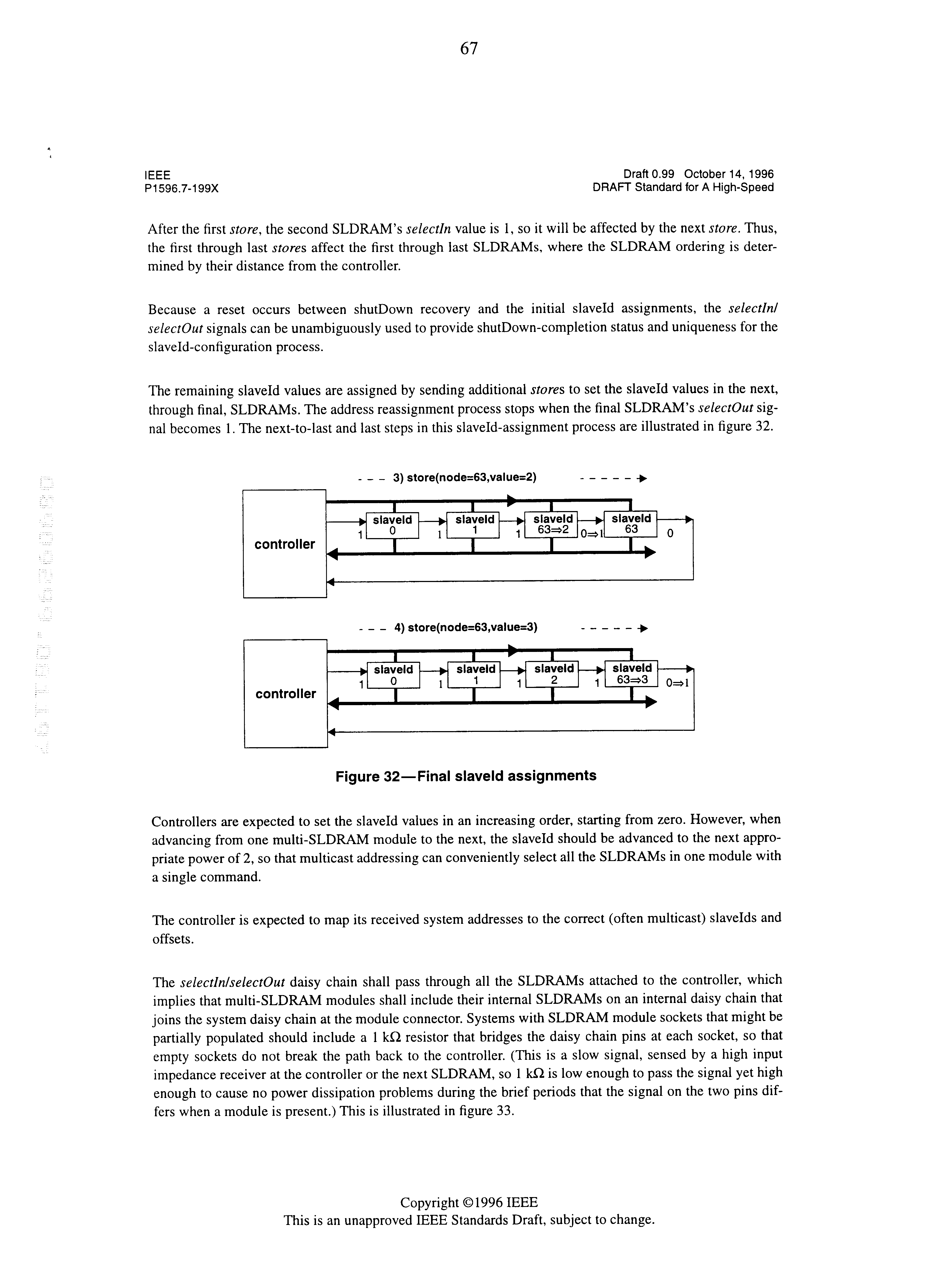
- the controller 36 sets selectOut and sends store packets 102 to the aforementioned registers to update the slaveIds to their final distinct values.
- the selectIn and selectOut are connected in a daisy chain configuration, shown more clearly in FIG. 4 . In this fashion, only the first of the unconfigured memory modules 34 processes the store packets 102 and changes its address and its selectOut signal. After the information packet 102 corresponding to the Store protocol is received by the second memory module 34 , the selectIn value associated therewith is 1, so it will be affected by the next information packet 102 corresponding to the Store protocol. Thus, the first through last information packets 102 affect the first through last memory module 34 , where the memory module 34 ordering is determined by their position in the daisy chain.
- the selectIn/selectOut signals can be unambiguously used to provide shutdown completion status and uniqueness for the slaveId-configuration process.
- the remaining slaveId values are assigned by sending additional information packets 102 stores to set the slaveId values in the remaining memory modules 34 .
- the address reassignment process stops when the final memory modules 34 's selectOut signal becomes 1.
- the controller 36 typically sets the slaveId values in an increasing order, starting from zero. However, when advancing between multi-memory module devices 30 , the slaveId value should be advanced to the next appropriate power of 2, so that multicast addressing can conveniently select all the memory modules 34 in one memory device 30 with a single command.
- the controller is expected to map its received system addresses to the correct (often multicast) slaveIds and offsets.
- each socket of the module include a resistor 39 that bridges the pins of each socket that correspond to the selectIn and selectOut pins of the memory modules 34 .
- the resistor 39 should be of a value which permits passing the signal yet high enough to cause no power dissipation problems during the brief periods that the signal on the two pins differ when a module is present.
- a 1 k ⁇ is employed to allow the relatively slow selectIn /selectOut signal to be sensed by the high input impedance receiver at the controller 36 or the selectIn pin of a memory module 34 .
- a 1 k ⁇ resistor is coupled in series between the selectIn and selectOut pins of each socket for a memory module 34 .
- the proper value is recorded for the read protocol delay register 76 of each of the memory modules 34 .
- This synchronizes the each memory module 34 so that transfers of data information on the dataLink occurs at the appropriate time.
- the memory device 30 initially powers up, an internal feedback in the memory module 34 adjusts the dataLink delay register 76 to synchronize the memory module outputs. Thereafter, the internal sync feedback is disabled and the controller 36 transmits to each specific memory modules 34 an information packet 106 corresponding to the load protocol, shown in FIG. 10 .
- the load protocol includes 011, following the SlaveId values.
- the subcommand is 0xx, and the packet contains a 7-bit index, specifying an internal control register, for example output register 64 , within the addressed memory module 34 from which data information is to be transmitted onto the dataLink.
- the memory module 34 emits a dataSync pattern on the dataLink: all 1-bits for one clock cycle, then all 0-bits for three clock cycles.
- the controller 36 may repeat this event as necessary, observing that data transitions (from 1 to 0), and storing corrected values in the read protocol delay register 76 with an information packet corresponding to the store protocol until all the memory modules 34 emit their load data at the time established by the controller 36 .
- the range of the adjustment steps is approximately one-sixteenth of a clock cycle.
- controller 36 compensates by adding integer clock cycles to the response by means of the read protocol delay register 76 as necessary to keep the delays within operating range.
- the controller 36 may transmit the load protocol to any memory module 34 of the array 32 so that each will concurrently provide the aforementioned dataSync pattern at the controller 36 , at the within a small fraction of a clock cycle.
- each of the memory modules 34 of the array 32 sample input write data information with the correct timing. This is done by sending a dataSync pattern from the controller 36 to the memory module 34 with an information packet 110 corresponding to a writeSync protocol, shown in FIG. 11 .
- the information packet 110 of corresponding to the writeSync protocol includes the values 111 , following the SlaveId values.
- the subcommand is 11x, and the remainder of the packet contains 0's. The results in preparation of the memory module 34 to receive a wave of 1's and 0's on the dataLink while the controller 36 .
- the writeSync protocol differs from a normal write in that the memory module 34 stores the received data in status register 66 rather than in the memory cells, where it would corrupt data information present therein.
- the data information received by the status register 66 is then read back by the controller 36 , using the load protocol, and compared with the desired results.
- the controller 36 then stores new values in the write protocol delay register 78 to adjust the timing of same.
- the controller 36 repeats syncWrite protocol, varying the write protocol delay register 78 timing in order to find a range of values that cause the data information to be strobed correctly.
- the controller 36 sets the write protocol delay register 78 proximate to the mid-point of this range. This facilitates maintaining synchronous data transfers on the dataLink so that a incoming data information is stable the values are latched. In this fashion, compensation may be made for clock-buffering delays and differences between the length of the commandLink path and the dataLink path.
- an intermediate power level is provided by a standBy protocol.
- the strobe signal and a listen signal are transmitted on the commandLink 40 .
- Other data receivers and drivers in the high-bandwidth interface 60 are disabled, thus saving about 80% of I/O power.
- the listen signal is synchronous, with the same transition timing as flag values and data information.
- the listen signal shall go to 1 before an information packet, and may drop to 0 any time after a packet.
- the controller 36 transmits the listen signal the flag value and data information remain unasserted (no idles are output).
- the controller 36 and memory modules 34 may immediately release the other drivers and receivers, leaving dataLink in an undefined state.
- the StandBy protocol has no effect on the memory module 34 's operational characteristics. Controllers 36 are expected to reactivate the memory modules 34 occasionally to perform autorefresh operations.
- a more severe mode of power conservation is attained with the shutdown protocol, which effectively shuts the memory device 30 down. More time is required for the memory device 30 to recover after the shutdown protocol is effectuated, than the time necessary for the memory device 30 to recover from intermediate power level.
- the shutdown protocol forces the memory modules 34 to enable their selfrefresh circuitry. Existing slaveId values remain unchanged.
- the controller 36 drives the linkOn signal low to put the memory modules 34 into the power down mode employing the shutdown protocol.
- the power down mode is entered from the intermediate power level, so a delay of t sbOff is defined between the receipt of the listen signal deasserted transition and the high assertion of the linkOn signal.
- t sbOff is required between the receipt of the standBy packet and the high-to-low transition of linkOn. Since linkOn is not a high speed signal, it is not relied on for precise timing in this protocol.
- the memory module 34 ignores further strobe and flag inputs, but shall ensure the validity of its selectOut signal until time t sbOffSlow . Maintaining valid outputs while ignoring the inputs helps compensate for potential linkOn-signal skew between controller 36 and memory modules 34 .
- a minimum power down time t sbDown is specified.
- shutdown recovery is initiated by the low-to-high transition of the linkOn signal.
- memory modules 34 drive their selectOut to zero.
- time t sbOnSlow memory modules 34 ignore input signals; at that time, they may adjust their input receivers based on the strobe signal.
- the memory modules 34 's receiver circuits shall be synchronized within t lock . After that time, and after completing any selfrefresh operation that may be in progress, the memory module allows the selectIn signal to propagate to the selectOut output, with a delay not to exceed t sdThru .
- the selectIn /selectOut signal are expected to be daisy-chained through all memory modules 34 , and the controller 36 delays packet transmissions until detecting a 1-valued selectOut signal from the final memory module 34 in the daisy chain.
- ROMs read only memory device
- PROMs programmable read only memory device
Abstract
Description
| TABLE 1 |
| SlaveId Values |
| slaveId | Description |
| 0-63 | Dynamically allocated |
| 63 | Initial identifier assignment |
| 64-126 | Multicast or broadcast read or write |
| 127 | Sync-pattern address |
| TABLE 2 |
| Command and Subcommand Encoding |
| Command | FromRow | Size | Subcommand | R/W | LeaveRow | DataClock | Name |
| 000 | Open | 4 | 000 | Read | Open | Even | |
| 000 | Open | 4 | 001 | Read | Open | Odd | |
| 000 | Open | 4 | 010 | Read | Closed | Even | |
| 000 | Open | 4 | 011 | Read | Closed | Odd | |
| 000 | Open | 4 | 100 | Write | Open | Even | |
| 000 | Open | 4 | 101 | Write | Open | Odd | |
| 000 | Open | 4 | 110 | Write | Closed | Even | |
| 000 | Open | 4 | 111 | Write | Closed | Odd | |
| 001 | Open | 8 | 000 | Read | Open | Even | |
| 001 | Open | 8 | 001 | Read | Open | Odd | |
| 001 | Open | 8 | 010 | Read | Closed | Even | |
| 001 | Open | 8 | 011 | Read | Closed | Odd | |
| 001 | Open | 8 | 100 | Write | Open | Even | |
| 001 | Open | 8 | 101 | Write | Open | Odd | |
| 001 | Open | 8 | 110 | Write | Closed | Even | |
| 001 | Open | 8 | 111 | Write | Closed | Odd | |
| 010 | Open | 16 | 000 | Read | Open | Even | |
| 010 | Open | 16 | 001 | Read | Open | Odd | |
| 010 | Open | 16 | 010 | Read | Closed | Even | |
| 010 | Open | 16 | 011 | Read | Closed | Odd | |
| 010 | Open | 16 | 100 | Write | Open | Even | |
| 010 | Open | 16 | 101 | Write | Open | Odd | |
| 010 | Open | 16 | 110 | Write | Closed | Even | |
| 010 | Open | 16 | 111 | Write | Closed | Odd | |
| 011 | 0x0 | (R) | Even | Load | |||
| 011 | 0x1 | (R) | Odd | Load | |||
| 011 | 10x | (W) | Store | ||||
| 011 | 11x | (W) | Closed | CloseRow | |||
| 100 | Closed | 4 | 000 | Read | Open | Even | |
| 100 | Closed | 4 | 001 | Read | Open | Odd | |
| 100 | Closed | 4 | 010 | Read | Closed | Even | |
| 100 | Closed | 4 | 011 | Read | Closed | Odd | |
| 100 | Closed | 4 | 100 | Write | Open | Even | |
| 100 | Closed | 4 | 101 | Write | Open | Odd | |
| 100 | Closed | 4 | 110 | Write | Closed | Even | |
| 100 | Closed | 4 | 111 | Write | Closed | Odd | |
| 101 | Closed | 8 | 000 | Read | Open | Even | |
| 101 | Closed | 8 | 001 | Read | Open | Odd | |
| 101 | Closed | 8 | 010 | Read | Closed | Even | |
| 101 | Closed | 8 | 011 | Read | Closed | Odd | |
| 101 | Closed | 8 | 100 | Write | Open | Even | |
| 101 | Closed | 8 | 101 | Write | Open | Odd | |
| 101 | Closed | 8 | 110 | Write | Closed | Even | |
| 101 | Closed | 8 | 111 | Write | Closed | Odd | |
| 110 | Closed | 16 | 000 | Read | Open | Even | |
| 110 | Closed | 16 | 001 | Read | Open | Odd | |
| 110 | Closed | 16 | 010 | Read | Closed | Even | |
| 110 | Closed | 16 | 011 | Read | Closed | Odd | |
| 110 | Closed | 16 | 100 | Write | Open | Even | |
| 110 | Closed | 16 | 101 | Write | Open | Odd | |
| 110 | Closed | 16 | 110 | Write | Closed | Even | |
| 110 | Closed | 16 | 111 | Write | Closed | Odd | |
| 111 | 000 | (R) | Sync | ||||
| (NoOp) | |||||||
| 111 | 001-011 | (R) | Reserved | ||||
| 111 | 10x | (W) | Event | ||||
| 111 | 11x | (W) | Write/ | ||||
| Sync | |||||||
| TABLE 3 |
| Event Protocol Index Codes |
| | Command | Description | |
| 0 | | Take slaveId | 63, initialize to reset |
| 1 | resetSoft | Initialize to reset state | |
| 2 | | Autorefresh signal | |
| 3 | closeRows | Close all open rows | |
| 4 | increaseA | Increase the input sample delay one |
|
| 5 | decreaseA | Decrease the input sample delay one |
|
| 6 | increaseB | Increase the output signal delay one |
|
| 7 | decreaseB | Decrease the output signal delay one step | |
| 8-63 | — | Reserved | |
| 64-127 | dependent | Vendor dependent | |


Claims (18)
Priority Applications (3)
| Application Number | Priority Date | Filing Date | Title |
|---|---|---|---|
| US08/909,299 US6226723B1 (en) | 1996-09-20 | 1997-08-11 | Bifurcated data and command/address communication bus architecture for random access memories employing synchronous communication protocols |
| US08/987,328 US6249827B1 (en) | 1997-08-11 | 1997-12-09 | Method for transferring data associated with a read/write command between a processor and a reader circuit using a plurality of clock lines |
| US10/176,327 US20030126356A1 (en) | 1997-08-11 | 2002-06-19 | Memory system having synchronous-link DRAM (SLDRAM) devices and controller |
Applications Claiming Priority (3)
| Application Number | Priority Date | Filing Date | Title |
|---|---|---|---|
| US2641996P | 1996-09-20 | 1996-09-20 | |
| US2689696P | 1996-09-20 | 1996-09-20 | |
| US08/909,299 US6226723B1 (en) | 1996-09-20 | 1997-08-11 | Bifurcated data and command/address communication bus architecture for random access memories employing synchronous communication protocols |
Related Parent Applications (1)
| Application Number | Title | Priority Date | Filing Date |
|---|---|---|---|
| US08/933,713 Continuation US5917760A (en) | 1996-09-20 | 1997-09-19 | De-skewing data signals in a memory system |
Related Child Applications (1)
| Application Number | Title | Priority Date | Filing Date |
|---|---|---|---|
| US10/176,327 Continuation US20030126356A1 (en) | 1997-08-11 | 2002-06-19 | Memory system having synchronous-link DRAM (SLDRAM) devices and controller |
Publications (1)
| Publication Number | Publication Date |
|---|---|
| US6226723B1 true US6226723B1 (en) | 2001-05-01 |
Family
ID=27362767
Family Applications (1)
| Application Number | Title | Priority Date | Filing Date |
|---|---|---|---|
| US08/909,299 Expired - Fee Related US6226723B1 (en) | 1996-09-20 | 1997-08-11 | Bifurcated data and command/address communication bus architecture for random access memories employing synchronous communication protocols |
Country Status (1)
| Country | Link |
|---|---|
| US (1) | US6226723B1 (en) |
Cited By (33)
| Publication number | Priority date | Publication date | Assignee | Title |
|---|---|---|---|---|
| EP1253521A2 (en) * | 2001-04-24 | 2002-10-30 | Rambus Inc. | Method and apparatus for signaling between devices of a memory system |
| US20020178324A1 (en) * | 1997-10-10 | 2002-11-28 | Rambus Inc. | High performance cost optimized memory |
| US6546476B1 (en) | 1996-09-20 | 2003-04-08 | Advanced Memory International, Inc. | Read/write timing for maximum utilization of bi-directional read/write bus |
| US6590907B1 (en) * | 1999-10-01 | 2003-07-08 | Stmicroelectronics Ltd. | Integrated circuit with additional ports |
| US6601126B1 (en) * | 2000-01-20 | 2003-07-29 | Palmchip Corporation | Chip-core framework for systems-on-a-chip |
| US20040054845A1 (en) * | 2001-04-24 | 2004-03-18 | Rambus, Inc. | Method and apparatus for signaling between devices of a memory system |
| US20040141404A1 (en) * | 1997-10-10 | 2004-07-22 | Rambus Inc. | Power control system for synchronous memory device |
| US20040158744A1 (en) * | 1999-04-01 | 2004-08-12 | Netscreen Technologies, Inc., A Delaware Corporation | Firewall including local bus |
| US20040230718A1 (en) * | 2003-05-13 | 2004-11-18 | Advanced Micro Devices, Inc. | System including a host connected to a plurality of memory modules via a serial memory interconnet |
| US6842864B1 (en) * | 1998-03-10 | 2005-01-11 | Rambus Inc. | Method and apparatus for configuring access times of memory devices |
| US20060039227A1 (en) * | 2004-08-17 | 2006-02-23 | Lawrence Lai | Memory device having staggered memory operations |
| US20060059299A1 (en) * | 1997-10-10 | 2006-03-16 | Barth Richard M | Apparatus and method for pipelined memory operations |
| US20070088995A1 (en) * | 2005-09-26 | 2007-04-19 | Rambus Inc. | System including a buffered memory module |
| US20070162685A1 (en) * | 2006-01-09 | 2007-07-12 | Jungwon Suh | Memory data bus structure and method of transferring information with plural memory banks |
| US20070177436A1 (en) * | 1997-10-10 | 2007-08-02 | Davis Paul G | Memory System and Method for Two Step Memory Write Operations |
| US20070206429A1 (en) * | 2004-09-15 | 2007-09-06 | Ware Frederick A | Memory component with multiple delayed timing signals |
| WO2007130640A2 (en) * | 2006-05-04 | 2007-11-15 | Inapac Technology, Inc. | Memory device including multiplexed inputs |
| US20080034130A1 (en) * | 2000-01-05 | 2008-02-07 | Rambus Inc. | Buffered Memory Having A Control Bus And Dedicated Data Lines |
| US20080109596A1 (en) * | 2000-01-05 | 2008-05-08 | Rambus Inc. | System Having A Controller Device, A Buffer Device And A Plurality Of Memory Devices |
| US7466603B2 (en) | 2006-10-03 | 2008-12-16 | Inapac Technology, Inc. | Memory accessing circuit system |
| US7562271B2 (en) | 2005-09-26 | 2009-07-14 | Rambus Inc. | Memory system topologies including a buffer device and an integrated circuit memory device |
| US20110078387A1 (en) * | 2009-09-28 | 2011-03-31 | International Business Machines Corporation | Writing to memory using shared address buses |
| US20110078392A1 (en) * | 2009-09-28 | 2011-03-31 | International Business Machines Corporation | Writing to memory using adaptive write techniques |
| US20110228600A1 (en) * | 2009-02-24 | 2011-09-22 | International Business Machines Corporation | Memory programming |
| US20120210089A1 (en) * | 2004-08-19 | 2012-08-16 | Round Rock Research, Llc | Memory command delay balancing in a daisy-chained memory topology |
| US8320202B2 (en) | 2001-04-24 | 2012-11-27 | Rambus Inc. | Clocked memory system with termination component |
| US8463985B2 (en) | 2010-03-31 | 2013-06-11 | International Business Machines Corporation | Constrained coding to reduce floating gate coupling in non-volatile memories |
| US8588017B2 (en) | 2010-10-20 | 2013-11-19 | Samsung Electronics Co., Ltd. | Memory circuits, systems, and modules for performing DRAM refresh operations and methods of operating the same |
| US9140441B2 (en) | 2012-08-15 | 2015-09-22 | Cree, Inc. | LED downlight |
| US9244867B1 (en) * | 2011-06-01 | 2016-01-26 | Altera Corporation | Memory controller interface with adjustable port widths |
| US20160164661A1 (en) * | 2014-12-09 | 2016-06-09 | Mediatek Inc. | Apparatus and method for transmitting and receiving data |
| US10108542B2 (en) * | 2016-01-04 | 2018-10-23 | Avalanche Technology, Inc. | Serial link storage interface (SLSI) hybrid block storage |
| US11328764B2 (en) | 2005-09-26 | 2022-05-10 | Rambus Inc. | Memory system topologies including a memory die stack |
Citations (12)
| Publication number | Priority date | Publication date | Assignee | Title |
|---|---|---|---|---|
| US4366538A (en) * | 1980-10-31 | 1982-12-28 | Honeywell Information Systems Inc. | Memory controller with queue control apparatus |
| US4954992A (en) | 1987-12-24 | 1990-09-04 | Mitsubishi Denki Kabushiki Kaisha | Random access memory having separate read out and write in bus lines for reduced access time and operating method therefor |
| US5058051A (en) * | 1988-07-29 | 1991-10-15 | Texas Medical Instruments, Inc. | Address register processor system |
| US5289431A (en) | 1991-10-29 | 1994-02-22 | Mitsubishi Denki Kabushiki Kaisha | Semiconductor memory device divided into blocks and operable to read and write data through different data lines and operation method of the same |
| US5307314A (en) | 1991-07-15 | 1994-04-26 | Micron Technology, Inc. | Split read/write dynamic random access memory |
| US5323349A (en) | 1991-10-31 | 1994-06-21 | Mitsubishi Denki Kabushiki Kaisha | Dynamic semiconductor memory device having separate read and write data bases |
| US5394541A (en) * | 1990-07-17 | 1995-02-28 | Sun Microsystems, Inc. | Programmable memory timing method and apparatus for programmably generating generic and then type specific memory timing signals |
| US5596731A (en) | 1995-04-21 | 1997-01-21 | Cyrix Corporation | Single clock bus transfers during burst and non-burst cycles |
| US5737587A (en) * | 1991-11-05 | 1998-04-07 | Monolithic System Technology, Inc. | Resynchronization circuit for circuit module architecture |
| US5805873A (en) * | 1994-11-30 | 1998-09-08 | Hitachi Micro Systems, Inc. | Phase linking of output clock with master clock in memory architecture |
| US5813038A (en) * | 1994-10-14 | 1998-09-22 | Compaq Computer Corporation | Memory controller having precharge prediction based on processor and PC bus cycles |
| US5831925A (en) * | 1996-12-03 | 1998-11-03 | Texas Instruments Incorporated | Memory configuration circuit and method |
-
1997
- 1997-08-11 US US08/909,299 patent/US6226723B1/en not_active Expired - Fee Related
Patent Citations (12)
| Publication number | Priority date | Publication date | Assignee | Title |
|---|---|---|---|---|
| US4366538A (en) * | 1980-10-31 | 1982-12-28 | Honeywell Information Systems Inc. | Memory controller with queue control apparatus |
| US4954992A (en) | 1987-12-24 | 1990-09-04 | Mitsubishi Denki Kabushiki Kaisha | Random access memory having separate read out and write in bus lines for reduced access time and operating method therefor |
| US5058051A (en) * | 1988-07-29 | 1991-10-15 | Texas Medical Instruments, Inc. | Address register processor system |
| US5394541A (en) * | 1990-07-17 | 1995-02-28 | Sun Microsystems, Inc. | Programmable memory timing method and apparatus for programmably generating generic and then type specific memory timing signals |
| US5307314A (en) | 1991-07-15 | 1994-04-26 | Micron Technology, Inc. | Split read/write dynamic random access memory |
| US5289431A (en) | 1991-10-29 | 1994-02-22 | Mitsubishi Denki Kabushiki Kaisha | Semiconductor memory device divided into blocks and operable to read and write data through different data lines and operation method of the same |
| US5323349A (en) | 1991-10-31 | 1994-06-21 | Mitsubishi Denki Kabushiki Kaisha | Dynamic semiconductor memory device having separate read and write data bases |
| US5737587A (en) * | 1991-11-05 | 1998-04-07 | Monolithic System Technology, Inc. | Resynchronization circuit for circuit module architecture |
| US5813038A (en) * | 1994-10-14 | 1998-09-22 | Compaq Computer Corporation | Memory controller having precharge prediction based on processor and PC bus cycles |
| US5805873A (en) * | 1994-11-30 | 1998-09-08 | Hitachi Micro Systems, Inc. | Phase linking of output clock with master clock in memory architecture |
| US5596731A (en) | 1995-04-21 | 1997-01-21 | Cyrix Corporation | Single clock bus transfers during burst and non-burst cycles |
| US5831925A (en) * | 1996-12-03 | 1998-11-03 | Texas Instruments Incorporated | Memory configuration circuit and method |
Cited By (140)
| Publication number | Priority date | Publication date | Assignee | Title |
|---|---|---|---|---|
| US6546476B1 (en) | 1996-09-20 | 2003-04-08 | Advanced Memory International, Inc. | Read/write timing for maximum utilization of bi-directional read/write bus |
| US20050160241A1 (en) * | 1997-10-10 | 2005-07-21 | Rambus Inc. | High performance cost optimized memory |
| US20070198868A1 (en) * | 1997-10-10 | 2007-08-23 | Barth Richard M | Memory System Having Delayed Write Timing |
| US7353357B2 (en) | 1997-10-10 | 2008-04-01 | Rambus Inc. | Apparatus and method for pipelined memory operations |
| US20100046314A1 (en) * | 1997-10-10 | 2010-02-25 | Tsern Ely K | Memory Device Having a Read Pipeline and a Delay Locked Loop |
| US7793039B2 (en) | 1997-10-10 | 2010-09-07 | Rambus Inc. | Interface for a semiconductor memory device and method for controlling the interface |
| US20090031093A1 (en) * | 1997-10-10 | 2009-01-29 | Davis Paul G | Memory System and Method for Two Step Memory Write Operations |
| US20040141404A1 (en) * | 1997-10-10 | 2004-07-22 | Rambus Inc. | Power control system for synchronous memory device |
| US20100332719A1 (en) * | 1997-10-10 | 2010-12-30 | Barth Richard M | Memory Write Signaling and Methods Thereof |
| US8560797B2 (en) | 1997-10-10 | 2013-10-15 | Rambus Inc. | Method and apparatus for indicating mask information |
| US7870357B2 (en) | 1997-10-10 | 2011-01-11 | Rambus Inc. | Memory system and method for two step memory write operations |
| US6868474B2 (en) * | 1997-10-10 | 2005-03-15 | Rambus Inc. | High performance cost optimized memory |
| US7986584B2 (en) | 1997-10-10 | 2011-07-26 | Rambus Inc. | Memory device having multiple power modes |
| US20080091907A1 (en) * | 1997-10-10 | 2008-04-17 | Barth Richard M | Integrated circuit memory device having delayed write timing based on read response time |
| US8019958B2 (en) | 1997-10-10 | 2011-09-13 | Rambus Inc. | Memory write signaling and methods thereof |
| US7626880B2 (en) | 1997-10-10 | 2009-12-01 | Rambus Inc. | Memory device having a read pipeline and a delay locked loop |
| US20050180255A1 (en) * | 1997-10-10 | 2005-08-18 | Tsern Ely K. | Memory device having a read pipeline and a delay locked loop |
| US20020178324A1 (en) * | 1997-10-10 | 2002-11-28 | Rambus Inc. | High performance cost optimized memory |
| US7330951B2 (en) | 1997-10-10 | 2008-02-12 | Rambus Inc. | Apparatus and method for pipelined memory operations |
| US7320082B2 (en) | 1997-10-10 | 2008-01-15 | Rambus Inc. | Power control system for synchronous memory device |
| US20080002516A1 (en) * | 1997-10-10 | 2008-01-03 | Tsern Ely K | Memory Device Having a Delay Locked Loop and Multiple Power Modes |
| US8504790B2 (en) | 1997-10-10 | 2013-08-06 | Rambus Inc. | Memory component having write operation with multiple time periods |
| US20060059299A1 (en) * | 1997-10-10 | 2006-03-16 | Barth Richard M | Apparatus and method for pipelined memory operations |
| US8140805B2 (en) | 1997-10-10 | 2012-03-20 | Rambus Inc. | Memory component having write operation with multiple time periods |
| US20070242532A1 (en) * | 1997-10-10 | 2007-10-18 | Barth Richard M | Integrated Circuit Memory Device Having Delayed Write Timing Based on Read Response Time |
| US8305839B2 (en) | 1997-10-10 | 2012-11-06 | Rambus Inc. | Memory device having multiple power modes |
| US20070140035A1 (en) * | 1997-10-10 | 2007-06-21 | Barth Richard M | Apparatus and Method for Pipelined Memory Operations |
| US20070147143A1 (en) * | 1997-10-10 | 2007-06-28 | Barth Richard M | Integrated Circuit Memory Device Having Delayed Write Capability |
| US20070159912A1 (en) * | 1997-10-10 | 2007-07-12 | Barth Richard M | Integrated Circuit Memory Device with Delayed Write Command Processing |
| US8248884B2 (en) | 1997-10-10 | 2012-08-21 | Rambus Inc. | Method of controlling a memory device having multiple power modes |
| US20070177436A1 (en) * | 1997-10-10 | 2007-08-02 | Davis Paul G | Memory System and Method for Two Step Memory Write Operations |
| US8205056B2 (en) | 1997-10-10 | 2012-06-19 | Rambus Inc. | Memory controller for controlling write signaling |
| US20050154817A1 (en) * | 1998-03-10 | 2005-07-14 | Barth Richard M. | Method of operation and controlling a memory device |
| US7574616B2 (en) | 1998-03-10 | 2009-08-11 | Rambus Inc. | Memory device having a power down exit register |
| US7571330B2 (en) | 1998-03-10 | 2009-08-04 | Rambus Inc. | System and module including a memory device having a power down mode |
| US8127152B2 (en) | 1998-03-10 | 2012-02-28 | Rambus Inc. | Method of operation of a memory device and system including initialization at a first frequency and operation at a second frequency and a power down exit mode |
| US20050235130A1 (en) * | 1998-03-10 | 2005-10-20 | Barth Richard M | System for a memory device having a power down mode and method |
| US20050216654A1 (en) * | 1998-03-10 | 2005-09-29 | Barth Richard M | System and module including a memory device having a power down mode |
| US7581121B2 (en) | 1998-03-10 | 2009-08-25 | Rambus Inc. | System for a memory device having a power down mode and method |
| US20050193183A1 (en) * | 1998-03-10 | 2005-09-01 | Barth Richard M. | Method and apparatus for initializing dynamic random access memory (DRAM) devices |
| US20050154853A1 (en) * | 1998-03-10 | 2005-07-14 | Barth Richard M. | Memory device and method of operation of a memory device |
| US8756395B2 (en) | 1998-03-10 | 2014-06-17 | Rambus Inc. | Controlling DRAM at time DRAM ready to receive command when exiting power down |
| US20050120161A1 (en) * | 1998-03-10 | 2005-06-02 | Barth Richard M. | Methods of operation of a memory device and system |
| US6842864B1 (en) * | 1998-03-10 | 2005-01-11 | Rambus Inc. | Method and apparatus for configuring access times of memory devices |
| US20050060487A1 (en) * | 1998-03-10 | 2005-03-17 | Barth Richard M. | Memory device having a power down exit register |
| US8490158B2 (en) | 1999-04-01 | 2013-07-16 | Juniper Networks, Inc. | Firewall including local bus |
| US20080209540A1 (en) * | 1999-04-01 | 2008-08-28 | Juniper Networks, Inc. | Firewall including local bus |
| US7363653B2 (en) * | 1999-04-01 | 2008-04-22 | Juniper Networks, Inc. | Firewall including local bus |
| US20040158744A1 (en) * | 1999-04-01 | 2004-08-12 | Netscreen Technologies, Inc., A Delaware Corporation | Firewall including local bus |
| US20100281532A1 (en) * | 1999-04-01 | 2010-11-04 | Juniper Networks, Inc. | Firewall including local bus |
| US7784093B2 (en) | 1999-04-01 | 2010-08-24 | Juniper Networks, Inc. | Firewall including local bus |
| US6590907B1 (en) * | 1999-10-01 | 2003-07-08 | Stmicroelectronics Ltd. | Integrated circuit with additional ports |
| US20080109596A1 (en) * | 2000-01-05 | 2008-05-08 | Rambus Inc. | System Having A Controller Device, A Buffer Device And A Plurality Of Memory Devices |
| US7526597B2 (en) | 2000-01-05 | 2009-04-28 | Rambus Inc. | Buffered memory having a control bus and dedicated data lines |
| US7523248B2 (en) | 2000-01-05 | 2009-04-21 | Rambus Inc. | System having a controller device, a buffer device and a plurality of memory devices |
| US20090319719A1 (en) * | 2000-01-05 | 2009-12-24 | Rambus Inc. | System Having A Controller Device, A Buffer Device And A Plurality Of Memory Devices |
| US20080034130A1 (en) * | 2000-01-05 | 2008-02-07 | Rambus Inc. | Buffered Memory Having A Control Bus And Dedicated Data Lines |
| US20040022107A1 (en) * | 2000-01-20 | 2004-02-05 | Palmchip Corporation | Unidirectional bus architecture for SoC applications |
| US6601126B1 (en) * | 2000-01-20 | 2003-07-29 | Palmchip Corporation | Chip-core framework for systems-on-a-chip |
| US7062587B2 (en) | 2000-01-20 | 2006-06-13 | Palmchip Corporation | Unidirectional bus architecture for SoC applications |
| US20070255919A1 (en) * | 2001-04-24 | 2007-11-01 | Ware Frederick A | Memory controller device having timing offset capability |
| US8359445B2 (en) | 2001-04-24 | 2013-01-22 | Rambus Inc. | Method and apparatus for signaling between devices of a memory system |
| US8537601B2 (en) | 2001-04-24 | 2013-09-17 | Rambus Inc. | Memory controller with selective data transmission delay |
| EP1253521A3 (en) * | 2001-04-24 | 2006-12-13 | Rambus Inc. | Method and apparatus for signaling between devices of a memory system |
| US8462566B2 (en) | 2001-04-24 | 2013-06-11 | Rambus Inc. | Memory module with termination component |
| US8625371B2 (en) | 2001-04-24 | 2014-01-07 | Rambus Inc. | Memory component with terminated and unterminated signaling inputs |
| US8395951B2 (en) | 2001-04-24 | 2013-03-12 | Rambus Inc. | Memory controller |
| US10706910B2 (en) | 2001-04-24 | 2020-07-07 | Rambus Inc. | Memory controller |
| US8391039B2 (en) | 2001-04-24 | 2013-03-05 | Rambus Inc. | Memory module with termination component |
| US8717837B2 (en) | 2001-04-24 | 2014-05-06 | Rambus Inc. | Memory module |
| US10236051B2 (en) | 2001-04-24 | 2019-03-19 | Rambus Inc. | Memory controller |
| US8320202B2 (en) | 2001-04-24 | 2012-11-27 | Rambus Inc. | Clocked memory system with termination component |
| US20040054845A1 (en) * | 2001-04-24 | 2004-03-18 | Rambus, Inc. | Method and apparatus for signaling between devices of a memory system |
| US9741424B2 (en) | 2001-04-24 | 2017-08-22 | Rambus Inc. | Memory controller |
| US9472262B2 (en) | 2001-04-24 | 2016-10-18 | Rambus Inc. | Memory controller |
| US8760944B2 (en) | 2001-04-24 | 2014-06-24 | Rambus Inc. | Memory component that samples command/address signals in response to both edges of a clock signal |
| US9311976B2 (en) | 2001-04-24 | 2016-04-12 | Rambus Inc. | Memory module |
| US8214616B2 (en) | 2001-04-24 | 2012-07-03 | Rambus Inc. | Memory controller device having timing offset capability |
| EP1253521A2 (en) * | 2001-04-24 | 2002-10-30 | Rambus Inc. | Method and apparatus for signaling between devices of a memory system |
| US9053778B2 (en) | 2001-04-24 | 2015-06-09 | Rambus Inc. | Memory controller that enforces strobe-to-strobe timing offset |
| US20040230718A1 (en) * | 2003-05-13 | 2004-11-18 | Advanced Micro Devices, Inc. | System including a host connected to a plurality of memory modules via a serial memory interconnet |
| US7421525B2 (en) * | 2003-05-13 | 2008-09-02 | Advanced Micro Devices, Inc. | System including a host connected to a plurality of memory modules via a serial memory interconnect |
| US8190808B2 (en) * | 2004-08-17 | 2012-05-29 | Rambus Inc. | Memory device having staggered memory operations |
| US20060039227A1 (en) * | 2004-08-17 | 2006-02-23 | Lawrence Lai | Memory device having staggered memory operations |
| US20120210089A1 (en) * | 2004-08-19 | 2012-08-16 | Round Rock Research, Llc | Memory command delay balancing in a daisy-chained memory topology |
| US8612712B2 (en) * | 2004-08-19 | 2013-12-17 | Round Rock Research, Llc | Memory command delay balancing in a daisy-chained memory topology |
| US8935505B2 (en) | 2004-08-19 | 2015-01-13 | Round Rock Research, Llc | System and method for controlling memory command delay |
| US8218382B2 (en) | 2004-09-15 | 2012-07-10 | Rambus Inc. | Memory component having a write-timing calibration mode |
| US20090063890A1 (en) * | 2004-09-15 | 2009-03-05 | Ware Frederick A | Memory controller with multiple delayed timing signals |
| US8743636B2 (en) | 2004-09-15 | 2014-06-03 | Rambus Inc. | Memory module having a write-timing calibration mode |
| US9437279B2 (en) | 2004-09-15 | 2016-09-06 | Rambus Inc. | Memory controller with clock-to-strobe skew compensation |
| US9229470B2 (en) | 2004-09-15 | 2016-01-05 | Rambus Inc. | Memory controller with clock-to-strobe skew compensation |
| US8363493B2 (en) | 2004-09-15 | 2013-01-29 | Rambus Inc. | Memory controller having a write-timing calibration mode |
| US10325645B2 (en) | 2004-09-15 | 2019-06-18 | Rambus Inc. | Memory controller with clock-to-strobe skew compensation |
| US9830971B2 (en) | 2004-09-15 | 2017-11-28 | Rambus Inc. | Memory controller with clock-to-strobe skew compensation |
| US20100188911A1 (en) * | 2004-09-15 | 2010-07-29 | Ware Frederick A | Memory-write timing calibration including generation of multiple delayed timing signals |
| US10755764B2 (en) | 2004-09-15 | 2020-08-25 | Rambus Inc. | Memory component that enables calibrated command- and data-timing signal arrival |
| US11100976B2 (en) | 2004-09-15 | 2021-08-24 | Rambus Inc. | Memory controller with clock-to-strobe skew compensation |
| US7724590B2 (en) | 2004-09-15 | 2010-05-25 | Rambus Inc. | Memory controller with multiple delayed timing signals |
| US8493802B1 (en) | 2004-09-15 | 2013-07-23 | Rambus Inc. | Memory controller having a write-timing calibration mode |
| US20070206429A1 (en) * | 2004-09-15 | 2007-09-06 | Ware Frederick A | Memory component with multiple delayed timing signals |
| US8045407B2 (en) | 2004-09-15 | 2011-10-25 | Rambus Inc. | Memory-write timing calibration including generation of multiple delayed timing signals |
| US11664067B2 (en) | 2004-09-15 | 2023-05-30 | Rambus Inc. | Memory system component that enables clock-to-strobe skew compensation |
| US8108607B2 (en) | 2005-09-26 | 2012-01-31 | Rambus Inc. | Memory system topologies including a buffer device and an integrated circuit memory device |
| US9563583B2 (en) | 2005-09-26 | 2017-02-07 | Rambus Inc. | Memory system topologies including a buffer device and an integrated circuit memory device |
| US8539152B2 (en) | 2005-09-26 | 2013-09-17 | Rambus Inc. | Memory system topologies including a buffer device and an integrated circuit memory device |
| US11727982B2 (en) | 2005-09-26 | 2023-08-15 | Rambus Inc. | Memory system topologies including a memory die stack |
| US7685364B2 (en) | 2005-09-26 | 2010-03-23 | Rambus Inc. | Memory system topologies including a buffer device and an integrated circuit memory device |
| US20070088995A1 (en) * | 2005-09-26 | 2007-04-19 | Rambus Inc. | System including a buffered memory module |
| US11328764B2 (en) | 2005-09-26 | 2022-05-10 | Rambus Inc. | Memory system topologies including a memory die stack |
| US7729151B2 (en) | 2005-09-26 | 2010-06-01 | Rambus Inc. | System including a buffered memory module |
| US11043258B2 (en) | 2005-09-26 | 2021-06-22 | Rambus Inc. | Memory system topologies including a memory die stack |
| US20100146199A1 (en) * | 2005-09-26 | 2010-06-10 | Rambus Inc. | Memory System Topologies Including A Buffer Device And An Integrated Circuit Memory Device |
| US20090198924A1 (en) * | 2005-09-26 | 2009-08-06 | Rambus Inc. | Memory System Topologies Including A Buffer Device And An Integrated Circuit Memory Device |
| US9117035B2 (en) | 2005-09-26 | 2015-08-25 | Rambus Inc. | Memory system topologies including a buffer device and an integrated circuit memory device |
| US7562271B2 (en) | 2005-09-26 | 2009-07-14 | Rambus Inc. | Memory system topologies including a buffer device and an integrated circuit memory device |
| US10672458B1 (en) | 2005-09-26 | 2020-06-02 | Rambus Inc. | Memory system topologies including a buffer device and an integrated circuit memory device |
| US10535398B2 (en) | 2005-09-26 | 2020-01-14 | Rambus Inc. | Memory system topologies including a buffer device and an integrated circuit memory device |
| US20110228614A1 (en) * | 2005-09-26 | 2011-09-22 | Rambus Inc. | Memory System Topologies Including A Buffer Device And An Integrated Circuit Memory Device |
| US10381067B2 (en) | 2005-09-26 | 2019-08-13 | Rambus Inc. | Memory system topologies including a buffer device and an integrated circuit memory device |
| US7464225B2 (en) | 2005-09-26 | 2008-12-09 | Rambus Inc. | Memory module including a plurality of integrated circuit memory devices and a plurality of buffer devices in a matrix topology |
| US9865329B2 (en) | 2005-09-26 | 2018-01-09 | Rambus Inc. | Memory system topologies including a buffer device and an integrated circuit memory device |
| US7359252B2 (en) | 2006-01-09 | 2008-04-15 | Infineon Technologies Ag | Memory data bus structure and method of transferring information with plural memory banks |
| US20070162685A1 (en) * | 2006-01-09 | 2007-07-12 | Jungwon Suh | Memory data bus structure and method of transferring information with plural memory banks |
| WO2007130640A2 (en) * | 2006-05-04 | 2007-11-15 | Inapac Technology, Inc. | Memory device including multiplexed inputs |
| WO2007130640A3 (en) * | 2006-05-04 | 2008-05-08 | Inapac Technology Inc | Memory device including multiplexed inputs |
| US7466603B2 (en) | 2006-10-03 | 2008-12-16 | Inapac Technology, Inc. | Memory accessing circuit system |
| US8897062B2 (en) | 2009-02-24 | 2014-11-25 | International Business Machines Corporation | Memory programming for a phase change memory cell |
| US20110228600A1 (en) * | 2009-02-24 | 2011-09-22 | International Business Machines Corporation | Memory programming |
| US8386739B2 (en) * | 2009-09-28 | 2013-02-26 | International Business Machines Corporation | Writing to memory using shared address buses |
| US20110078392A1 (en) * | 2009-09-28 | 2011-03-31 | International Business Machines Corporation | Writing to memory using adaptive write techniques |
| US20110078387A1 (en) * | 2009-09-28 | 2011-03-31 | International Business Machines Corporation | Writing to memory using shared address buses |
| US8230276B2 (en) | 2009-09-28 | 2012-07-24 | International Business Machines Corporation | Writing to memory using adaptive write techniques |
| US8463985B2 (en) | 2010-03-31 | 2013-06-11 | International Business Machines Corporation | Constrained coding to reduce floating gate coupling in non-volatile memories |
| US8588017B2 (en) | 2010-10-20 | 2013-11-19 | Samsung Electronics Co., Ltd. | Memory circuits, systems, and modules for performing DRAM refresh operations and methods of operating the same |
| US9244867B1 (en) * | 2011-06-01 | 2016-01-26 | Altera Corporation | Memory controller interface with adjustable port widths |
| US9140441B2 (en) | 2012-08-15 | 2015-09-22 | Cree, Inc. | LED downlight |
| US20160164661A1 (en) * | 2014-12-09 | 2016-06-09 | Mediatek Inc. | Apparatus and method for transmitting and receiving data |
| US9800398B2 (en) * | 2014-12-09 | 2017-10-24 | Mediatek Inc. | Apparatus and method for transmitting and receiving data |
| US10108542B2 (en) * | 2016-01-04 | 2018-10-23 | Avalanche Technology, Inc. | Serial link storage interface (SLSI) hybrid block storage |
Similar Documents
| Publication | Publication Date | Title |
|---|---|---|
| US6226723B1 (en) | Bifurcated data and command/address communication bus architecture for random access memories employing synchronous communication protocols | |
| US7404032B2 (en) | Configurable width buffered module having switch elements | |
| US6889284B1 (en) | Method and apparatus for supporting SDRAM memory | |
| US7200710B2 (en) | Buffer device and method of operation in a buffer device | |
| US7356639B2 (en) | Configurable width buffered module having a bypass circuit | |
| US6502161B1 (en) | Memory system including a point-to-point linked memory subsystem | |
| US6970968B1 (en) | Memory module controller for providing an interface between a system memory controller and a plurality of memory devices on a memory module | |
| US8751754B2 (en) | Memory systems and methods for controlling the timing of receiving read data | |
| US6968419B1 (en) | Memory module having a memory module controller controlling memory transactions for a plurality of memory devices | |
| EP1036362B1 (en) | Memory system including a memory module having a memory module controller | |
| US7266634B2 (en) | Configurable width buffered module having flyby elements | |
| US7730254B2 (en) | Memory buffer for an FB-DIMM | |
| US20070005922A1 (en) | Fully buffered DIMM variable read latency | |
| US11947474B2 (en) | Multi-mode memory module and memory component | |
| KR20070092318A (en) | Memory buffers for merging local data from memory modules | |
| US20070286010A1 (en) | Identical chips with different operations in a system | |
| US20050010737A1 (en) | Configurable width buffered module having splitter elements | |
| US20090019184A1 (en) | Interfacing memory devices | |
| JP4578676B2 (en) | Apparatus and method for compensating device timing | |
| US20040230759A1 (en) | Synchronous memory system and also method and protocol for communication in a synchronous memory system | |
| US20230022530A1 (en) | Data buffer for memory devices with unidirectional ports | |
| US20100299486A1 (en) | Electronic Devices and Methods for Storing Data in a Memory | |
| KR20150073336A (en) | Memory cell and memory module having the same | |
| KR100916215B1 (en) | Protocol memory, memory module, protocl memory system and method for controlling thereof |
Legal Events
| Date | Code | Title | Description |
|---|---|---|---|
| AS | Assignment |
Owner name: SLDRAM, INCORPORATED, CALIFORNIA Free format text: ASSIGNMENT OF ASSIGNORS INTEREST;ASSIGNORS:GUSTAVSON, DAVID B.;JAMES, DAVID V.;WIGGERS, HANS A.;REEL/FRAME:009051/0693 Effective date: 19980310 |
|
| AS | Assignment |
Owner name: HEWLETT-PACKARD COMPANY, CALIFORNIA Free format text: ASSIGNMENT OF ASSIGNORS INTEREST;ASSIGNOR:WIGGERS, HANS A.;REEL/FRAME:009217/0270 Effective date: 19980310 |
|
| AS | Assignment |
Owner name: GUSTAVSON, DAVID B., CALIFORNIA Free format text: ASSIGNMENT OF ASSIGNORS INTEREST;ASSIGNOR:SCIZZL;REEL/FRAME:009285/0536 Effective date: 19980618 Owner name: GUSTAVSON, DAVID B., CALIFORNIA Free format text: ASSIGNMENT OF ASSIGNORS INTEREST;ASSIGNOR:SANTA CLARA UNIVERSITY;REEL/FRAME:009285/0569 Effective date: 19980522 Owner name: SLDRAM, INC., CALIFORNIA Free format text: ASSIGNMENT OF ASSIGNORS INTEREST;ASSIGNOR:GUSTAVSON, DAVID B.;REEL/FRAME:009292/0300 Effective date: 19980618 |
|
| AS | Assignment |
Owner name: ADVANCED MEMORY INTERNATIONAL, INC., CALIFORNIA Free format text: CHANGE OF NAME;ASSIGNOR:SLDRAM, INC.;REEL/FRAME:010649/0888 Effective date: 19990409 |
|
| AS | Assignment |
Owner name: HEWLETT-PACKARD COMPANY, COLORADO Free format text: MERGER;ASSIGNOR:HEWLETT-PACKARD COMPANY;REEL/FRAME:011523/0469 Effective date: 19980520 |
|
| CC | Certificate of correction | ||
| FPAY | Fee payment |
Year of fee payment: 4 |
|
| REMI | Maintenance fee reminder mailed | ||
| LAPS | Lapse for failure to pay maintenance fees | ||
| STCH | Information on status: patent discontinuation |
Free format text: PATENT EXPIRED DUE TO NONPAYMENT OF MAINTENANCE FEES UNDER 37 CFR 1.362 |
|
| FP | Lapsed due to failure to pay maintenance fee |
Effective date: 20090501 |