US6228694B1 - Method of increasing the mobility of MOS transistors by use of localized stress regions - Google Patents
Method of increasing the mobility of MOS transistors by use of localized stress regions Download PDFInfo
- Publication number
- US6228694B1 US6228694B1 US09/340,583 US34058399A US6228694B1 US 6228694 B1 US6228694 B1 US 6228694B1 US 34058399 A US34058399 A US 34058399A US 6228694 B1 US6228694 B1 US 6228694B1
- Authority
- US
- United States
- Prior art keywords
- regions
- substrate
- transistors
- substance
- implanting
- Prior art date
- Legal status (The legal status is an assumption and is not a legal conclusion. Google has not performed a legal analysis and makes no representation as to the accuracy of the status listed.)
- Expired - Lifetime
Links
- 238000000034 method Methods 0.000 title claims abstract description 42
- 239000000758 substrate Substances 0.000 claims abstract description 75
- 239000000126 substance Substances 0.000 claims abstract description 39
- 238000000137 annealing Methods 0.000 claims description 9
- QVGXLLKOCUKJST-UHFFFAOYSA-N atomic oxygen Chemical compound [O] QVGXLLKOCUKJST-UHFFFAOYSA-N 0.000 claims description 5
- 229910052756 noble gas Inorganic materials 0.000 claims description 5
- 150000002835 noble gases Chemical class 0.000 claims description 5
- 239000001301 oxygen Substances 0.000 claims description 5
- 229910052760 oxygen Inorganic materials 0.000 claims description 5
- 239000000969 carrier Substances 0.000 claims description 4
- 238000002347 injection Methods 0.000 claims description 3
- 239000007924 injection Substances 0.000 claims description 3
- 230000000873 masking effect Effects 0.000 claims 4
- 239000011800 void material Substances 0.000 abstract description 6
- 230000037230 mobility Effects 0.000 description 42
- 239000007943 implant Substances 0.000 description 13
- 238000002513 implantation Methods 0.000 description 11
- 230000000694 effects Effects 0.000 description 7
- 230000004888 barrier function Effects 0.000 description 5
- 230000007423 decrease Effects 0.000 description 5
- 230000015572 biosynthetic process Effects 0.000 description 4
- 239000001307 helium Substances 0.000 description 4
- 229910052734 helium Inorganic materials 0.000 description 4
- SWQJXJOGLNCZEY-UHFFFAOYSA-N helium atom Chemical compound [He] SWQJXJOGLNCZEY-UHFFFAOYSA-N 0.000 description 4
- 239000003112 inhibitor Substances 0.000 description 4
- XUIMIQQOPSSXEZ-UHFFFAOYSA-N Silicon Chemical compound [Si] XUIMIQQOPSSXEZ-UHFFFAOYSA-N 0.000 description 3
- 239000007789 gas Substances 0.000 description 3
- 239000000463 material Substances 0.000 description 3
- 229920002120 photoresistant polymer Polymers 0.000 description 3
- 229910052710 silicon Inorganic materials 0.000 description 3
- 239000010703 silicon Substances 0.000 description 3
- XKRFYHLGVUSROY-UHFFFAOYSA-N Argon Chemical compound [Ar] XKRFYHLGVUSROY-UHFFFAOYSA-N 0.000 description 2
- 125000004429 atom Chemical group 0.000 description 2
- 238000006243 chemical reaction Methods 0.000 description 2
- 238000007796 conventional method Methods 0.000 description 2
- 150000002500 ions Chemical class 0.000 description 2
- 238000004519 manufacturing process Methods 0.000 description 2
- 229910021420 polycrystalline silicon Inorganic materials 0.000 description 2
- 229920005591 polysilicon Polymers 0.000 description 2
- 239000004065 semiconductor Substances 0.000 description 2
- ZOXJGFHDIHLPTG-UHFFFAOYSA-N Boron Chemical compound [B] ZOXJGFHDIHLPTG-UHFFFAOYSA-N 0.000 description 1
- 238000005280 amorphization Methods 0.000 description 1
- 229910052786 argon Inorganic materials 0.000 description 1
- 229910052785 arsenic Inorganic materials 0.000 description 1
- RQNWIZPPADIBDY-UHFFFAOYSA-N arsenic atom Chemical compound [As] RQNWIZPPADIBDY-UHFFFAOYSA-N 0.000 description 1
- 238000005452 bending Methods 0.000 description 1
- 229910052796 boron Inorganic materials 0.000 description 1
- 230000002860 competitive effect Effects 0.000 description 1
- 230000003247 decreasing effect Effects 0.000 description 1
- 230000005684 electric field Effects 0.000 description 1
- 239000003623 enhancer Substances 0.000 description 1
- 125000005843 halogen group Chemical group 0.000 description 1
- BHEPBYXIRTUNPN-UHFFFAOYSA-N hydridophosphorus(.) (triplet) Chemical compound [PH] BHEPBYXIRTUNPN-UHFFFAOYSA-N 0.000 description 1
- 230000009545 invasion Effects 0.000 description 1
- 229910052751 metal Inorganic materials 0.000 description 1
- 239000002184 metal Substances 0.000 description 1
- 230000003071 parasitic effect Effects 0.000 description 1
- 230000035945 sensitivity Effects 0.000 description 1
Images


Classifications
-
- H—ELECTRICITY
- H01—ELECTRIC ELEMENTS
- H01L—SEMICONDUCTOR DEVICES NOT COVERED BY CLASS H10
- H01L21/00—Processes or apparatus adapted for the manufacture or treatment of semiconductor or solid state devices or of parts thereof
- H01L21/02—Manufacture or treatment of semiconductor devices or of parts thereof
- H01L21/04—Manufacture or treatment of semiconductor devices or of parts thereof the devices having at least one potential-jump barrier or surface barrier, e.g. PN junction, depletion layer or carrier concentration layer
- H01L21/18—Manufacture or treatment of semiconductor devices or of parts thereof the devices having at least one potential-jump barrier or surface barrier, e.g. PN junction, depletion layer or carrier concentration layer the devices having semiconductor bodies comprising elements of Group IV of the Periodic System or AIIIBV compounds with or without impurities, e.g. doping materials
- H01L21/26—Bombardment with radiation
- H01L21/263—Bombardment with radiation with high-energy radiation
- H01L21/265—Bombardment with radiation with high-energy radiation producing ion implantation
- H01L21/26506—Bombardment with radiation with high-energy radiation producing ion implantation in group IV semiconductors
-
- H—ELECTRICITY
- H01—ELECTRIC ELEMENTS
- H01L—SEMICONDUCTOR DEVICES NOT COVERED BY CLASS H10
- H01L21/00—Processes or apparatus adapted for the manufacture or treatment of semiconductor or solid state devices or of parts thereof
- H01L21/70—Manufacture or treatment of devices consisting of a plurality of solid state components formed in or on a common substrate or of parts thereof; Manufacture of integrated circuit devices or of parts thereof
- H01L21/77—Manufacture or treatment of devices consisting of a plurality of solid state components or integrated circuits formed in, or on, a common substrate
- H01L21/78—Manufacture or treatment of devices consisting of a plurality of solid state components or integrated circuits formed in, or on, a common substrate with subsequent division of the substrate into plural individual devices
- H01L21/82—Manufacture or treatment of devices consisting of a plurality of solid state components or integrated circuits formed in, or on, a common substrate with subsequent division of the substrate into plural individual devices to produce devices, e.g. integrated circuits, each consisting of a plurality of components
- H01L21/822—Manufacture or treatment of devices consisting of a plurality of solid state components or integrated circuits formed in, or on, a common substrate with subsequent division of the substrate into plural individual devices to produce devices, e.g. integrated circuits, each consisting of a plurality of components the substrate being a semiconductor, using silicon technology
- H01L21/8232—Field-effect technology
- H01L21/8234—MIS technology, i.e. integration processes of field effect transistors of the conductor-insulator-semiconductor type
- H01L21/823412—MIS technology, i.e. integration processes of field effect transistors of the conductor-insulator-semiconductor type with a particular manufacturing method of the channel structures, e.g. channel implants, halo or pocket implants, or channel materials
-
- H—ELECTRICITY
- H01—ELECTRIC ELEMENTS
- H01L—SEMICONDUCTOR DEVICES NOT COVERED BY CLASS H10
- H01L21/00—Processes or apparatus adapted for the manufacture or treatment of semiconductor or solid state devices or of parts thereof
- H01L21/70—Manufacture or treatment of devices consisting of a plurality of solid state components formed in or on a common substrate or of parts thereof; Manufacture of integrated circuit devices or of parts thereof
- H01L21/77—Manufacture or treatment of devices consisting of a plurality of solid state components or integrated circuits formed in, or on, a common substrate
- H01L21/78—Manufacture or treatment of devices consisting of a plurality of solid state components or integrated circuits formed in, or on, a common substrate with subsequent division of the substrate into plural individual devices
- H01L21/82—Manufacture or treatment of devices consisting of a plurality of solid state components or integrated circuits formed in, or on, a common substrate with subsequent division of the substrate into plural individual devices to produce devices, e.g. integrated circuits, each consisting of a plurality of components
- H01L21/822—Manufacture or treatment of devices consisting of a plurality of solid state components or integrated circuits formed in, or on, a common substrate with subsequent division of the substrate into plural individual devices to produce devices, e.g. integrated circuits, each consisting of a plurality of components the substrate being a semiconductor, using silicon technology
- H01L21/8232—Field-effect technology
- H01L21/8234—MIS technology, i.e. integration processes of field effect transistors of the conductor-insulator-semiconductor type
- H01L21/823418—MIS technology, i.e. integration processes of field effect transistors of the conductor-insulator-semiconductor type with a particular manufacturing method of the source or drain structures, e.g. specific source or drain implants or silicided source or drain structures or raised source or drain structures
-
- H—ELECTRICITY
- H01—ELECTRIC ELEMENTS
- H01L—SEMICONDUCTOR DEVICES NOT COVERED BY CLASS H10
- H01L29/00—Semiconductor devices adapted for rectifying, amplifying, oscillating or switching, or capacitors or resistors with at least one potential-jump barrier or surface barrier, e.g. PN junction depletion layer or carrier concentration layer; Details of semiconductor bodies or of electrodes thereof ; Multistep manufacturing processes therefor
- H01L29/02—Semiconductor bodies ; Multistep manufacturing processes therefor
- H01L29/06—Semiconductor bodies ; Multistep manufacturing processes therefor characterised by their shape; characterised by the shapes, relative sizes, or dispositions of the semiconductor regions ; characterised by the concentration or distribution of impurities within semiconductor regions
- H01L29/0603—Semiconductor bodies ; Multistep manufacturing processes therefor characterised by their shape; characterised by the shapes, relative sizes, or dispositions of the semiconductor regions ; characterised by the concentration or distribution of impurities within semiconductor regions characterised by particular constructional design considerations, e.g. for preventing surface leakage, for controlling electric field concentration or for internal isolations regions
- H01L29/0642—Isolation within the component, i.e. internal isolation
- H01L29/0649—Dielectric regions, e.g. SiO2 regions, air gaps
- H01L29/0653—Dielectric regions, e.g. SiO2 regions, air gaps adjoining the input or output region of a field-effect device, e.g. the source or drain region
-
- H—ELECTRICITY
- H01—ELECTRIC ELEMENTS
- H01L—SEMICONDUCTOR DEVICES NOT COVERED BY CLASS H10
- H01L29/00—Semiconductor devices adapted for rectifying, amplifying, oscillating or switching, or capacitors or resistors with at least one potential-jump barrier or surface barrier, e.g. PN junction depletion layer or carrier concentration layer; Details of semiconductor bodies or of electrodes thereof ; Multistep manufacturing processes therefor
- H01L29/02—Semiconductor bodies ; Multistep manufacturing processes therefor
- H01L29/30—Semiconductor bodies ; Multistep manufacturing processes therefor characterised by physical imperfections; having polished or roughened surface
- H01L29/32—Semiconductor bodies ; Multistep manufacturing processes therefor characterised by physical imperfections; having polished or roughened surface the imperfections being within the semiconductor body
-
- H—ELECTRICITY
- H01—ELECTRIC ELEMENTS
- H01L—SEMICONDUCTOR DEVICES NOT COVERED BY CLASS H10
- H01L29/00—Semiconductor devices adapted for rectifying, amplifying, oscillating or switching, or capacitors or resistors with at least one potential-jump barrier or surface barrier, e.g. PN junction depletion layer or carrier concentration layer; Details of semiconductor bodies or of electrodes thereof ; Multistep manufacturing processes therefor
- H01L29/66—Types of semiconductor device ; Multistep manufacturing processes therefor
- H01L29/68—Types of semiconductor device ; Multistep manufacturing processes therefor controllable by only the electric current supplied, or only the electric potential applied, to an electrode which does not carry the current to be rectified, amplified or switched
- H01L29/76—Unipolar devices, e.g. field effect transistors
- H01L29/772—Field effect transistors
- H01L29/78—Field effect transistors with field effect produced by an insulated gate
- H01L29/7842—Field effect transistors with field effect produced by an insulated gate means for exerting mechanical stress on the crystal lattice of the channel region, e.g. using a flexible substrate
Definitions
- a method of modifying the carrier mobility of a transistor is described. More specifically, the present invention describes a method of utilizing implants in a substrate to induce a mechanical stress in the substrate to modify the carrier mobility of a transistor.
- FIG. 1 is a side cross-sectional view of an NMOS transistor 10 known in the art.
- a conventional transistor 10 generally includes a semiconductor generally comprising a silicon layer 16 having a source 20 and a drain 18 separated by a channel region 22 .
- a thin oxide layer 14 separates a gate 12 , generally comprising polysilicon, from the channel region 22 .
- the source 20 and drain 18 are n+ regions having been doped by arsenic or phosphorous.
- the channel region 22 is generally boron doped. (Note that for both the source 20 and drain 18 regions and the channel region 22 other materials may also be used.) Fabrication of a transistor such as the device 10 illustrated in FIG. 1 is well-known in the art and will not be discussed in detail herein.
- DIBL Drain-induced Barrier Lowering
- a method of modifying the carrier mobility of a transistor is described. First, a substance is implanted into a substrate. The substrate is then annealed such that the implanted substance forms at least one void in the substrate. Then, a transistor is formed on the substrate.
- FIG. 1 is a side cross-sectional view of an NMOS transistor known in the art.
- FIG. 2A is a side cross-sectional view of an MOS transistor under tensile stress.
- FIG. 2B is a side cross-sectional view of an MOS transistor under compressive stress.
- FIG. 3A is a graph illustrating the percent change in mobility of a transistor as a function of stress for an NMOS transistor.
- FIG. 3B is a graph illustrating the percent change in mobility of a transistor as a function of stress for a PMOS transistor.
- FIG. 4 is a side cross-sectional view of a substrate having gaseous implants.
- FIG. 5 is a side cross-sectional view of a substrate with a mask wherein the channel region of an NMOS device to be formed is exposed.
- FIG. 6 is a side cross-sectional view of the substrate of FIG. 5 undergoing gaseous implantation.
- FIG. 7 is a side cross-sectional view of the NMOS device of FIGS. 5 and 6 with voids in the channel region creating a tensile stress.
- FIG. 8 is a side cross-sectional view of a substrate with a mask wherein the source and drain regions of a PMOS device to be formed are exposed.
- FIG. 9 is a side cross-sectional view of the substrate of FIG. 8 undergoing gaseous implantation.
- FIG. 10 is a side cross-sectional view of the PMOS device of FIGS. 8 and 9 with voids in the source and drain regions creating a compressive stress.
- FIG. 11 is a side cross-sectional view of an MOS device having NMOS devices under tensile stress and PMOS devices under compressive stress.
- FIG. 12 is a side cross-sectional view of an MOS device having a graded stress effect created by the presence of voids in the source region.
- FIG. 13 is a side cross-sectional view of an NMOS device fabricated using conventional methods known in the art.
- FIG. 14 is a side cross-sectional view of the NMOS device of FIG. 13 with a mask leaving solely the gate exposed.
- FIG. 15 is a side cross-sectional view of the NMOS device of FIG. 14 during gaseous implantation.
- FIG. 16 is a side cross-sectional view of the NMOS device of FIG. 15 with gaseous implants in the gate creating a tensile stress in the device.
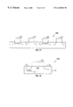
- FIG. 17 is a side cross-sectional view of an MOS device with a void in the channel region acting as a barrier to reduce current leakage.
- FIG. 18 is a side cross-sectional view of an MOS device with a plurality of voids near the source and drain regions along the outer portion of the channel that act as a barrier to reduce current leakage.
- One method of varying the carrier mobility of a transistor is by varying the bandgap. As the bandgap of a device decreases, the carrier mobility of the device increases. Likewise, as the bandgap of a device increases, the carrier mobility of the device decreases. Variation of the bandgap and hence variation of the carrier mobility of a transistor may be achieved by creating localized stresses across the different regions (i.e., source, drain, channel, and gate) of a transistor. Localized stresses in a substrate cause deformation of the substrate, which affects the size of the bandgap. It has been known for some time that in NMOS transistors, tensile (compressive) stresses cause increases (decreases) in mobility due to the sensitivity of the bandgap to stresses. Similarly, PMOS transistors show increases (decreases) in mobility due to compressive (tensile) stress. This change in mobility of a device arises due to energy level changes in the valance band caused by these stresses.
- FIG. 2A illustrates the NMOS transistor 10 (see FIG. 1) when a tensile stress is applied.
- the narrower channel region 24 results in a smaller bandgap and hence an increased mobility.
- FIG. 2B illustrates the NMOS transistor 10 (see FIG. 1) when a compressive stress is applied.
- the larger channel region 26 results in a larger bandgap and hence a decreased mobility. Note that in both FIGS. 2A and 2B the amount of localized stress has been greatly exaggerated for illustrative purposes only.
- FIGS. 3A and 3B illustrate the dependence of a device's carrier mobility on the mechanical stress applied to the device.
- FIG. 3A illustrates this dependence for an NMOS device
- FIG. 3B illustrates this dependence for a PMOS device.
- the dependence of a device's mobility on stress has been quantified, wherein changes in mechanical stress of the order of approximately 100 MPa can result in mobility changes of the order of approximately 4%.
- One method of creating localized stresses in a semiconductor is through the implantation of a substance (e.g., a gas) into the silicon substrate.
- a substance e.g., a gas
- the implantation of gaseous substances into the substrate results in the formation of voids (also referred to as cavities, openings, or bubbles) within the substrate, as illustrated in FIG. 4 .
- the implanted gaseous substance generally migrates or diffuses out of the substrate, leaving behind a void in the substrate.
- a method of forming voids in a region of a substrate to modify the localized stresses of the region such that the carrier mobility of a device fabricated on the substrate is also modified is described herein.
- the substrate is strained such that it bends the band and in bending the band changes the mobility of the carrier.
- the carrier mobility of a device is representative of an electron's ability to move through the channel region of a device under a given field.
- the voids of the present invention may be implanted into the substrate before, during, or after the formation of a device on the substrate. In one embodiment, however, the voids are implanted into a substrate prior to the formation of a device on the substrate.
- the substance to be implanted into the substrate may be any one of or a combination of several different gases, including but not limited to the noble gases. Oxygen or other implanted ions may also be used in reactions to alter the internal region of the substrate by way of specific volume or thermal expansion differences (e.g., oxidized voids).
- helium is the substance implanted into the substrate of the to-be-formed device. For illustrative purposes only, the following embodiments of the present invention will be discussed with use of helium-formed voids.
- a conventional implanter may be used to implant the substance into the substrate.
- the implantation is performed at an energy of approximately 30 keV (kilo electron volts) and a dosage of approximately 10 16 to 10 17 atoms/cm 2 .
- the depth of the implantation into the substrate is approximately 2000 ⁇ . Note that the depth of the implantation is controlled by the energy of the implant and may be modified as required by the size of a given device.
- the damage to the substrate may include vacancies, interstitials, dislocations, stacking faults, etc.
- the damage to the substrate begins to anneal away and the formation of voids in the substrate begins.
- the voids are approximately 10-20 nm wide when annealed at approximately 600° C. As the annealing temperature increases, the smaller voids become smaller and eventually disappear, and the larger voids become larger.
- the remaining voids are approximately 50 nm when annealed at approximately 1100° C. These voids can cause localized stresses of approximately 1 GPa.
- helium-formed voids are implanted in the channel region of an NMOS device as illustrated in FIGS. 5-7.
- a mask 52 is formed on a substrate 50 using conventional photoresist techniques, such that the region of the substrate 50 that will eventually be the channel region of NMOS device is exposed (see FIG. 5 ).
- helium is implanted to form voids 56 in the exposed region following the above described process and as illustrated in FIG. 6 .
- the mask 52 is removed and an NMOS device 64 shown in FIG. 7 is formed on the substrate 50 having a source 58 , a drain 60 , and a gate 62 with a channel region 59 under a localized stress.
- the resulting NMOS device 64 thus has an increased carrier mobility due to the tensile stresses on the device.
- a similar procedure is followed to create a PMOS device having helium-formed voids implanted in the source and drain regions of the device, as illustrated in FIGS. 8-10.
- a mask 82 is formed on a substrate 80 using conventional photoresist techniques, such that the regions of the substrate 80 that will eventually be the source and drain of a PMOS device are exposed (see FIG. 8 ).
- helium is implanted to form voids 86 in the exposed region following the above described process and as illustrated in FIG. 9 .
- the mask 82 is removed and a PMOS device 94 is formed on the substrate 80 having a source 88 , a drain 90 , a gate 92 , and a channel region 89 .
- the source 88 and drain region 90 are now under a localized stress resulting in a PMOS device 94 having an increased carrier mobility due to the compressive stresses on the device.
- NMOS devices have an increased carrier mobility when placed under a tensile stress and PMOS devices have an increased carrier mobility when placed under a compressive stress.
- a problem arises when the entire substrate is put under a tensile (compressive) stress, since the NMOS (PMOS) device's mobility will increase while the PMOS (NMOS) device's mobility will decrease.
- a third embodiment of the present invention involves placing the portion of a substrate to be used in an NMOS device under a tensile stress. This causes the remaining portion of the substrate, the portion to be used as a PMOS device, to be under a compressive stress. In this manner, the carrier mobility of both types of MOS devices may be increased even when formed from a single substrate.
- FIG. 11 illustrates a device 100 containing both NMOS devices 102 and PMOS devices 104 .
- Voids are formed in the channel region of the NMOS devices 102 .
- the voids create localized stresses such that the NMOS devices 102 are under a tensile stress and the PMOS devices 104 are under a compressive stress.
- both types of devices 102 and 104 have an increased carrier mobility.
- a fourth embodiment of the present invention creates an MOS device having a grading effect.
- An MOS device 110 having a grading effect is illustrated in FIG. 12 .
- voids 111 have been formed in the substrate 113 .
- the voids are formed solely below the source region 112 of the device 110 .
- the band structure at the source region 112 is placed under a tensile stress and the drain region 114 is placed under a compressive stress.
- Grading a transistor in this manner can create a device 110 that has greater drive current due to increased injection of carriers at the source end resulting from the band distortion induced by the voids.
- FIGS. 13-16 shows an alternative method of using voids to create a tensile stress in an NMOS device.
- FIG. 13 illustrates an NMOS device 120 having a source 122 , a gate 124 , a drain 126 , and a channel region 128 .
- the NMOS device 120 may be formed using conventional methods known in the art.
- a conventional photoresist mask 130 is applied to the device 120 such that only the gate 124 is exposed (see FIG. 14 ).
- voids 132 are formed in the gate 124 (note that the gate 124 may be either polysilicon or metal).
- the substance to be implanted into the gate may be any one of or a combination of several different gases, including but not limited to the noble gases. Oxygen or other implanted ions may also be used in reactions to alter the internal region of the gate by way of specific volume or thermal expansion differences (e.g. oxidized voids).
- argon is the substance implanted into the gate 124 of the NMOS transistor 120 .
- the implantation is performed at an energy of approximately 10 keV and a dosage of approximately 10 16 to 10 17 atoms/cm 2 , commensurate with an implant depth approximately halfway down into the gate, or approximately 1000 ⁇ .
- the device 120 is then annealed for approximately 30 seconds at at least 400° C.
- the implant and annealing process steps may be performed either before the gate is etched or after. If performed after, it may be necessary to protect the source 122 and drain 126 regions with the mask 130 as shown.
- the mask 130 is removed (see FIG. 16 )
- an NMOS device 134 under a tensile stress caused by the voids in the gate 124 is revealed and has an increased carrier mobility as compared to the NMOS device 120 of FIG. 13 .
- Each of the above embodiments has utilized implantations to modify the mechanical stresses acting on an MOS device.
- the present invention provides MOS devices having an increased carrier mobility. In this manner, the speed of MOS devices may be improved.
- DIBL Drain-Induced Barrier Lowering
- One use of the voids described above is to create a region between the source and drain that effectively inhibits the lines of force from the drain terminating at the source junction as shown in FIG. 17.
- a large single void 142 may be formed in the channel region 144 below the gate 149 of an MOS transistor 140 to effectively reduce leakage current between the source 146 and the drain 148 .
- An alternative embodiment achieves this same purpose of reducing leakage current through use of several smaller voids 152 formed at the outer edges of the channel region 154 below the gate 159 and near the source 156 and drain 158 regions, as shown in device 150 of FIG. 18 . In this manner, more competitive transistors may be designed since short channel effects will be reduced and, as a result, devices may be fabricated having a shorter channel length.
- the voids 142 and 152 used to inhibit the lines of force from the drain terminating at the source junction are formed by the same process as that described above with respect to the voids used to increase mobility.
- the same voids can act both as mobility enhancers and punch-through inhibitors.
- the placement of voids used as punch-through inhibitors in the substrate is more critical than voids used to induce localized stress regions.
- the punch-through inhibitor voids are implanted at approximately 1000 ⁇ into the substrate.
- the voids in the silicon act to reduce short channel effects (a very local effect).
- the punch-through inhibitor voids are generally closer to the channel than the mobility voids, and the mobility voids can be further away as long as the stresses are large enough to influence the mobility at the surface or channel region.
Abstract
A method of modifying the mobility of a transistor. First, a substance is implanted into a substrate. The substrate is then annealed such that the implanted substance forms at least one void in the substrate. Then, a transistor is formed on the substrate.
Description
1. Field of the Invention
A method of modifying the carrier mobility of a transistor is described. More specifically, the present invention describes a method of utilizing implants in a substrate to induce a mechanical stress in the substrate to modify the carrier mobility of a transistor.
2. Related Applications
Applications related to the present invention include: “Technique to Obtain Increased Channel Mobilities in NMOS Transistors by Gate Electrode Engineering”, Ser. No. 09/340,954, filed Jun. 28, 1999, “Methodology for Control of Short Channel Effects in MOS Transistors”, Ser. No. 09/342,0300, filed Jun. 28, 1999, and “Method for Reduced Capacitance Interconnect System Using Gaseous Implants into the ILD”, Ser. No. 09/344,918, filed Jun. 28, 1999. Each of the related applications listed above has been assigned to the Assignee of the present invention.
3. Description of Related Art
FIG. 1 is a side cross-sectional view of an NMOS transistor 10 known in the art. A conventional transistor 10 generally includes a semiconductor generally comprising a silicon layer 16 having a source 20 and a drain 18 separated by a channel region 22. A thin oxide layer 14 separates a gate 12, generally comprising polysilicon, from the channel region 22. In the device 10 illustrated in FIG. 1, the source 20 and drain 18 are n+ regions having been doped by arsenic or phosphorous. The channel region 22 is generally boron doped. (Note that for both the source 20 and drain 18 regions and the channel region 22 other materials may also be used.) Fabrication of a transistor such as the device 10 illustrated in FIG. 1 is well-known in the art and will not be discussed in detail herein.
The speed or velocity (v) of the current through the channel region 22 is a function of the mobility (μ) of the channel region, as expressed by the formula v=μE wherein E represents the electric field across the channel region 22. Because E is generally a constant value, the higher the carrier mobility (μ) of a device the faster the device can function. As the demand for faster devices continually grows in the industry, the desire for a device having an increased mobility also increases. Thus, a method for fabricating a device having an increased carrier mobility would be desirable.
Another issue that arises when dealing with transistors of the present art involves current leakage from the source to the drain. One of the limiting factors in the scaling of transistors to smaller dimensions is the inability of the gate to fully control the channel region below the gate. As the source and drain junctions approach one another, the lines of force resulting from the potential applied to the drain terminate on the source junction, causing Drain-induced Barrier Lowering (DIBL). This DIBL results in leakage current between the source and drain, and at short enough channel lengths, results in failure of the device. Thus, a method of reducing current leakage would allow for the fabrication of transistors fabricated on a smaller scale.
A method of modifying the carrier mobility of a transistor is described. First, a substance is implanted into a substrate. The substrate is then annealed such that the implanted substance forms at least one void in the substrate. Then, a transistor is formed on the substrate.
The invention is further described by way of example with reference to the accompanying drawings, wherein:
FIG. 1 is a side cross-sectional view of an NMOS transistor known in the art. FIG. 2A is a side cross-sectional view of an MOS transistor under tensile stress.
FIG. 2B is a side cross-sectional view of an MOS transistor under compressive stress.
FIG. 3A is a graph illustrating the percent change in mobility of a transistor as a function of stress for an NMOS transistor.
FIG. 3B is a graph illustrating the percent change in mobility of a transistor as a function of stress for a PMOS transistor.
FIG. 4 is a side cross-sectional view of a substrate having gaseous implants.
FIG. 5 is a side cross-sectional view of a substrate with a mask wherein the channel region of an NMOS device to be formed is exposed.
FIG. 6 is a side cross-sectional view of the substrate of FIG. 5 undergoing gaseous implantation.
FIG. 7 is a side cross-sectional view of the NMOS device of FIGS. 5 and 6 with voids in the channel region creating a tensile stress.
FIG. 8 is a side cross-sectional view of a substrate with a mask wherein the source and drain regions of a PMOS device to be formed are exposed.
FIG. 9 is a side cross-sectional view of the substrate of FIG. 8 undergoing gaseous implantation.
FIG. 10 is a side cross-sectional view of the PMOS device of FIGS. 8 and 9 with voids in the source and drain regions creating a compressive stress.
FIG. 11 is a side cross-sectional view of an MOS device having NMOS devices under tensile stress and PMOS devices under compressive stress.
FIG. 12 is a side cross-sectional view of an MOS device having a graded stress effect created by the presence of voids in the source region.
FIG. 13 is a side cross-sectional view of an NMOS device fabricated using conventional methods known in the art.
FIG. 14 is a side cross-sectional view of the NMOS device of FIG. 13 with a mask leaving solely the gate exposed.
FIG. 15 is a side cross-sectional view of the NMOS device of FIG. 14 during gaseous implantation.
FIG. 16 is a side cross-sectional view of the NMOS device of FIG. 15 with gaseous implants in the gate creating a tensile stress in the device.
FIG. 17 is a side cross-sectional view of an MOS device with a void in the channel region acting as a barrier to reduce current leakage.
FIG. 18 is a side cross-sectional view of an MOS device with a plurality of voids near the source and drain regions along the outer portion of the channel that act as a barrier to reduce current leakage.
A method of varying the carrier mobility of a transistor through use of implants is described. In the following description, numerous specific details are set forth such as specific materials, process parameters, dimensions, etc. in order to provide a thorough understanding of the present invention. It will be obvious, however, to one skilled in the art that these specific details need not be employed to practice the present invention. In other instances, well-known materials or methods have not been described in detail in order to avoid unnecessarily obscuring the present invention.
One method of varying the carrier mobility of a transistor is by varying the bandgap. As the bandgap of a device decreases, the carrier mobility of the device increases. Likewise, as the bandgap of a device increases, the carrier mobility of the device decreases. Variation of the bandgap and hence variation of the carrier mobility of a transistor may be achieved by creating localized stresses across the different regions (i.e., source, drain, channel, and gate) of a transistor. Localized stresses in a substrate cause deformation of the substrate, which affects the size of the bandgap. It has been known for some time that in NMOS transistors, tensile (compressive) stresses cause increases (decreases) in mobility due to the sensitivity of the bandgap to stresses. Similarly, PMOS transistors show increases (decreases) in mobility due to compressive (tensile) stress. This change in mobility of a device arises due to energy level changes in the valance band caused by these stresses.
FIG. 2A illustrates the NMOS transistor 10 (see FIG. 1) when a tensile stress is applied. The narrower channel region 24 results in a smaller bandgap and hence an increased mobility. FIG. 2B illustrates the NMOS transistor 10 (see FIG. 1) when a compressive stress is applied. The larger channel region 26 results in a larger bandgap and hence a decreased mobility. Note that in both FIGS. 2A and 2B the amount of localized stress has been greatly exaggerated for illustrative purposes only. FIGS. 3A and 3B illustrate the dependence of a device's carrier mobility on the mechanical stress applied to the device. FIG. 3A illustrates this dependence for an NMOS device and FIG. 3B illustrates this dependence for a PMOS device. As illustrated in FIGS. 3A and 3B, the dependence of a device's mobility on stress has been quantified, wherein changes in mechanical stress of the order of approximately 100 MPa can result in mobility changes of the order of approximately 4%.
One method of creating localized stresses in a semiconductor is through the implantation of a substance (e.g., a gas) into the silicon substrate. The implantation of gaseous substances into the substrate results in the formation of voids (also referred to as cavities, openings, or bubbles) within the substrate, as illustrated in FIG. 4. As the substrate undergoes subsequent processing, the implanted gaseous substance generally migrates or diffuses out of the substrate, leaving behind a void in the substrate.
A method of forming voids in a region of a substrate to modify the localized stresses of the region such that the carrier mobility of a device fabricated on the substrate is also modified is described herein. By introducing a void in the substrate of a device, the substrate is strained such that it bends the band and in bending the band changes the mobility of the carrier. Recall from the previous discussion above, the carrier mobility of a device is representative of an electron's ability to move through the channel region of a device under a given field.
The voids of the present invention may be implanted into the substrate before, during, or after the formation of a device on the substrate. In one embodiment, however, the voids are implanted into a substrate prior to the formation of a device on the substrate. The substance to be implanted into the substrate may be any one of or a combination of several different gases, including but not limited to the noble gases. Oxygen or other implanted ions may also be used in reactions to alter the internal region of the substrate by way of specific volume or thermal expansion differences (e.g., oxidized voids). In one embodiment of the present invention, helium is the substance implanted into the substrate of the to-be-formed device. For illustrative purposes only, the following embodiments of the present invention will be discussed with use of helium-formed voids.
The implantation of voids into a substrate is known and will not be discussed in detail herein. Thus, a conventional implanter may be used to implant the substance into the substrate. In one embodiment of the present invention, the implantation is performed at an energy of approximately 30 keV (kilo electron volts) and a dosage of approximately 1016 to 1017 atoms/cm2. In this embodiment, the depth of the implantation into the substrate is approximately 2000 Å. Note that the depth of the implantation is controlled by the energy of the implant and may be modified as required by the size of a given device.
As the substance is introduced into the substrate, damage is caused by the substance to the substrate, causing an amorphization of the lattice at the implant depth. The damage to the substrate may include vacancies, interstitials, dislocations, stacking faults, etc. As the substrate is annealed at approximately 400-500° C. and for approximately 30 seconds, the damage to the substrate begins to anneal away and the formation of voids in the substrate begins. In one embodiment of the present invention, the voids are approximately 10-20 nm wide when annealed at approximately 600° C. As the annealing temperature increases, the smaller voids become smaller and eventually disappear, and the larger voids become larger. For example, in one embodiment of the present invention, the remaining voids are approximately 50 nm when annealed at approximately 1100° C. These voids can cause localized stresses of approximately 1 GPa.
In one embodiment of the present invention, helium-formed voids are implanted in the channel region of an NMOS device as illustrated in FIGS. 5-7. First, a mask 52 is formed on a substrate 50 using conventional photoresist techniques, such that the region of the substrate 50 that will eventually be the channel region of NMOS device is exposed (see FIG. 5). Then, helium is implanted to form voids 56 in the exposed region following the above described process and as illustrated in FIG. 6. Once the helium has been implanted, the mask 52 is removed and an NMOS device 64 shown in FIG. 7 is formed on the substrate 50 having a source 58, a drain 60, and a gate 62 with a channel region 59 under a localized stress. The resulting NMOS device 64 thus has an increased carrier mobility due to the tensile stresses on the device.
In a second embodiment of the present invention, a similar procedure is followed to create a PMOS device having helium-formed voids implanted in the source and drain regions of the device, as illustrated in FIGS. 8-10. First, a mask 82 is formed on a substrate 80 using conventional photoresist techniques, such that the regions of the substrate 80 that will eventually be the source and drain of a PMOS device are exposed (see FIG. 8). Then, helium is implanted to form voids 86 in the exposed region following the above described process and as illustrated in FIG. 9. Once the voids 86 have been formed, the mask 82 is removed and a PMOS device 94 is formed on the substrate 80 having a source 88, a drain 90, a gate 92, and a channel region 89. The source 88 and drain region 90 are now under a localized stress resulting in a PMOS device 94 having an increased carrier mobility due to the compressive stresses on the device.
As discussed above, NMOS devices have an increased carrier mobility when placed under a tensile stress and PMOS devices have an increased carrier mobility when placed under a compressive stress. A problem arises when the entire substrate is put under a tensile (compressive) stress, since the NMOS (PMOS) device's mobility will increase while the PMOS (NMOS) device's mobility will decrease. Thus, a third embodiment of the present invention involves placing the portion of a substrate to be used in an NMOS device under a tensile stress. This causes the remaining portion of the substrate, the portion to be used as a PMOS device, to be under a compressive stress. In this manner, the carrier mobility of both types of MOS devices may be increased even when formed from a single substrate. FIG. 11 illustrates a device 100 containing both NMOS devices 102 and PMOS devices 104. Voids are formed in the channel region of the NMOS devices 102. The voids create localized stresses such that the NMOS devices 102 are under a tensile stress and the PMOS devices 104 are under a compressive stress. Thus, both types of devices 102 and 104 have an increased carrier mobility.
A fourth embodiment of the present invention creates an MOS device having a grading effect. One example of an MOS device 110 having a grading effect is illustrated in FIG. 12. In the same manner as that described above, voids 111 have been formed in the substrate 113. In this embodiment, however, the voids are formed solely below the source region 112 of the device 110. In this manner, the band structure at the source region 112 is placed under a tensile stress and the drain region 114 is placed under a compressive stress. Grading a transistor in this manner can create a device 110 that has greater drive current due to increased injection of carriers at the source end resulting from the band distortion induced by the voids.
Another embodiment illustrated in FIGS. 13-16 shows an alternative method of using voids to create a tensile stress in an NMOS device. FIG. 13 illustrates an NMOS device 120 having a source 122, a gate 124, a drain 126, and a channel region 128. The NMOS device 120 may be formed using conventional methods known in the art. After the NMOS device 120 is formed, a conventional photoresist mask 130 is applied to the device 120 such that only the gate 124 is exposed (see FIG. 14). Next, as shown in FIG. 15, voids 132 are formed in the gate 124 (note that the gate 124 may be either polysilicon or metal). As above, the substance to be implanted into the gate may be any one of or a combination of several different gases, including but not limited to the noble gases. Oxygen or other implanted ions may also be used in reactions to alter the internal region of the gate by way of specific volume or thermal expansion differences (e.g. oxidized voids). In one embodiment, argon is the substance implanted into the gate 124 of the NMOS transistor 120. In one embodiment, the implantation is performed at an energy of approximately 10 keV and a dosage of approximately 1016 to 1017 atoms/cm2, commensurate with an implant depth approximately halfway down into the gate, or approximately 1000 Å. The device 120 is then annealed for approximately 30 seconds at at least 400° C. The implant and annealing process steps may be performed either before the gate is etched or after. If performed after, it may be necessary to protect the source 122 and drain 126 regions with the mask 130 as shown. When the mask 130 is removed (see FIG. 16), an NMOS device 134 under a tensile stress caused by the voids in the gate 124 is revealed and has an increased carrier mobility as compared to the NMOS device 120 of FIG. 13.
Each of the above embodiments has utilized implantations to modify the mechanical stresses acting on an MOS device. By modifying the stresses acting upon a MOS device, the present invention provides MOS devices having an increased carrier mobility. In this manner, the speed of MOS devices may be improved.
Other uses of implants in the substrate of an MOS transistor are also significantly advantageous. For example, one of the limiting factors in the scaling of transistors to smaller dimensions is the inability of the gate to fully control the channel region. As the source and drain junctions approach one another, the lines of force resulting from the potential applied to the drain terminate on the source junction, causing Drain-Induced Barrier Lowering (DIBL). This DIBL results in leakage current between the source and drain, and at short enough channel lengths, results in failure of the device. One approach to limiting this parasitic effect is in use of punch-through implants and Halo implants to control the amount the barrier is lowered between the source and drain.
One use of the voids described above is to create a region between the source and drain that effectively inhibits the lines of force from the drain terminating at the source junction as shown in FIG. 17. A large single void 142 may be formed in the channel region 144 below the gate 149 of an MOS transistor 140 to effectively reduce leakage current between the source 146 and the drain 148. An alternative embodiment achieves this same purpose of reducing leakage current through use of several smaller voids 152 formed at the outer edges of the channel region 154 below the gate 159 and near the source 156 and drain 158 regions, as shown in device 150 of FIG. 18. In this manner, more competitive transistors may be designed since short channel effects will be reduced and, as a result, devices may be fabricated having a shorter channel length.
Note that the voids 142 and 152 used to inhibit the lines of force from the drain terminating at the source junction are formed by the same process as that described above with respect to the voids used to increase mobility. In fact, the same voids can act both as mobility enhancers and punch-through inhibitors. However, the placement of voids used as punch-through inhibitors in the substrate is more critical than voids used to induce localized stress regions. Typically, the punch-through inhibitor voids are implanted at approximately 1000 Å into the substrate. The voids in the silicon act to reduce short channel effects (a very local effect). As the stress increases, the mobility of carriers further and further from the voids are affected, eventually reaching all the way up to the invasion layer. Thus, the punch-through inhibitor voids are generally closer to the channel than the mobility voids, and the mobility voids can be further away as long as the stresses are large enough to influence the mobility at the surface or channel region.
Claims (24)
1. A method, comprising:
providing a plurality of first regions on a substrate alternating with a plurality of second regions on the substrate such that at least one second region is disposed between at least two first regions;
creating tensile stress in the first regions and compressive stress in the second regions by masking the second regions to prevent implanting a substance in the second regions and implanting the substance in the first regions to create voids in the first regions;
forming channel regions of a plurality of first transistors in the plurality of first regions; and
forming channel regions of a plurality of second transistors in the plurality of second regions.
2. The method of claim 1, further comprising:
forming first source and drain regions adjacent to each of the channel regions of the plurality of first transistors; and
forming second source and drain regions adjacent to each of the channel regions of the plurality of second transistors.
3. The method of claim 2, wherein the first source and drain regions are disposed in the first regions.
4. The method of claim 2, wherein the second source and drain regions are disposed in the second regions.
5. The method of claim 1, wherein the first transistors are NMOS transistors and the second transistors are PMOS transistors.
6. A plurality of first transistors and second transistors created by a process comprising:
providing a plurality of first regions on a substrate alternating with a plurality of second regions on the substrate such that at least one second region is disposed between at least two first regions;
creating tensile stress in the first regions and compressive stress in the second regions by masking the second regions to prevent implanting a substance in the second regions and implanting the substance in the first regions to create voids in the first regions;
forming channel regions of the plurality of first transistors in the plurality of first regions; and
forming channel regions of the plurality of second transistors in the plurality of second regions.
7. The plurality of first transistors and second transistors of claim 6, further comprising:
forming first source and drain regions adjacent to each of the channel regions of the plurality of first transistors; and
forming second source and drain regions adjacent to each of the channel regions of the plurality of second transistors.
8. The plurality of first transistors and second transistors of claim 7, wherein the first source and drain regions are disposed in the second regions.
9. The plurality of first transistors and second transistors of claim 7, wherein the second source and drain regions are disposed in the second regions.
10. The plurality of first transistors and second transistors of claim 6, wherein the first transistors are NMOS transistors and the second transistors are PMOS transistors.
11. A method of increasing injection of carriers in a transistor, comprising:
creating tensile stress in a first region of a substrate and compressive stress in a second region of the substrate by masking the second regions to prevent implanting a substance in the second regions and implanting the substance in the first region to create voids in the first region;
forming a source region of a transistor in the first region;
forming a channel region of the transistor and a drain region of the transistor in the second region.
12. A transistor with increased injection of carriers, created by a process comprising:
creating tensile stress in a first region of a substrate and compressive stress in a second region of the substrate by masking the second regions to prevent implanting a substance in the second regions and implanting the substance in the first region to create voids in the first region;
forming a source region of the transistor in the first region;
forming a channel region of the transistor and a drain region of the transistor in the second region.
13. The transistor of claim 12 wherein implanting a substance further comprises implanting a substance selected from the group consisting of the noble gases, oxygen, and any combination thereof.
14. The transistor of claim 12 wherein implanting a substance comprises annealing said substrate at at least 400° C. to form voids in said substrate.
15. The method of claim 1 wherein implanting a substance comprises implanting a substance selected from the group consisting of the noble gases, oxygen and any combination thereof.
16. The method of claim 1 wherein implanting a substance comprises implanting a substance at an energy level of approximately 30 keV.
17. The method of claim 16 wherein implanting a substance further comprises implanting a substance at a dosage of approximately 1016 to 1017 atoms/cm2.
18. The method of claim 1 wherein implanting a substance comprises annealing said substrate at at least 400° C. to form voids in said substrate.
19. The method of claim 18 wherein annealing said substrate further comprises annealing said substrate for at least 30 seconds.
20. The method of claim 18 wherein annealing said substrate further comprises annealing said substrate at approximately 1100° C.
21. The method of claim 11 wherein implanting a substance further comprises implanting a substance selected from the group consisting of the noble gases, oxygen, and any combination thereof.
22. The method of claim 11 wherein implanting a substance comprises implanting a substance at an energy level of approximately 30 keV.
23. The method of claim 22 wherein implanting a substance comprises implanting a substance at a dosage of approximately 1016 to 1017 atoms/cm2.
24. The method of claim 11 wherein implanting a substance comprises annealing said substrate at at least 400° C. to form voids in said substrate.
Priority Applications (1)
| Application Number | Priority Date | Filing Date | Title |
|---|---|---|---|
| US09/340,583 US6228694B1 (en) | 1999-06-28 | 1999-06-28 | Method of increasing the mobility of MOS transistors by use of localized stress regions |
Applications Claiming Priority (1)
| Application Number | Priority Date | Filing Date | Title |
|---|---|---|---|
| US09/340,583 US6228694B1 (en) | 1999-06-28 | 1999-06-28 | Method of increasing the mobility of MOS transistors by use of localized stress regions |
Publications (1)
| Publication Number | Publication Date |
|---|---|
| US6228694B1 true US6228694B1 (en) | 2001-05-08 |
Family
ID=23334029
Family Applications (1)
| Application Number | Title | Priority Date | Filing Date |
|---|---|---|---|
| US09/340,583 Expired - Lifetime US6228694B1 (en) | 1999-06-28 | 1999-06-28 | Method of increasing the mobility of MOS transistors by use of localized stress regions |
Country Status (1)
| Country | Link |
|---|---|
| US (1) | US6228694B1 (en) |
Cited By (132)
| Publication number | Priority date | Publication date | Assignee | Title |
|---|---|---|---|---|
| US6391695B1 (en) * | 2000-08-07 | 2002-05-21 | Advanced Micro Devices, Inc. | Double-gate transistor formed in a thermal process |
| US20020070419A1 (en) * | 2000-12-13 | 2002-06-13 | Farrar Paul A. | Method of forming buried conductor patterns by surface transformation of empty spaces in solid state materials |
| US20030030091A1 (en) * | 2001-08-13 | 2003-02-13 | Amberwave Systems Corporation | Dynamic random access memory trench capacitors |
| US20030052334A1 (en) * | 2001-06-18 | 2003-03-20 | Lee Minjoo L. | Structure and method for a high-speed semiconductor device |
| US20030133683A1 (en) * | 2002-01-17 | 2003-07-17 | Micron Technology, Inc. | Three-dimensional photonic crystal waveguide structure and method |
| US6656822B2 (en) * | 1999-06-28 | 2003-12-02 | Intel Corporation | Method for reduced capacitance interconnect system using gaseous implants into the ILD |
| US20030227029A1 (en) * | 2002-06-07 | 2003-12-11 | Amberwave Systems Corporation | Elevated source and drain elements for strained-channel heterojuntion field-effect transistors |
| US20040000268A1 (en) * | 1998-04-10 | 2004-01-01 | Massachusetts Institute Of Technology | Etch stop layer system |
| US20040005740A1 (en) * | 2002-06-07 | 2004-01-08 | Amberwave Systems Corporation | Strained-semiconductor-on-insulator device structures |
| US20040023874A1 (en) * | 2002-03-15 | 2004-02-05 | Burgess Catherine E. | Therapeutic polypeptides, nucleic acids encoding same, and methods of use |
| US6709955B2 (en) * | 2000-04-17 | 2004-03-23 | Stmicroelectronics S.R.L. | Method of fabricating electronic devices integrated in semiconductor substrates provided with gettering sites, and a device fabricated by the method |
| FR2846789A1 (en) * | 2002-11-05 | 2004-05-07 | St Microelectronics Sa | Semiconductor device with MOS transistors with an engraving stop layer having two levels of residual stress adapted to the nature of the transistors |
| US20040154083A1 (en) * | 2002-12-23 | 2004-08-12 | Mcvicker Henry J. | Sports pad closure system with integrally molded hooks |
| US20040164318A1 (en) * | 2001-08-06 | 2004-08-26 | Massachusetts Institute Of Technology | Structures with planar strained layers |
| US20040173812A1 (en) * | 2003-03-07 | 2004-09-09 | Amberwave Systems Corporation | Shallow trench isolation process |
| US20040173798A1 (en) * | 2003-03-05 | 2004-09-09 | Micron Technology, Inc. | Micro-mechanically strained semiconductor film |
| US20040176483A1 (en) * | 2003-03-05 | 2004-09-09 | Micron Technology, Inc. | Cellular materials formed using surface transformation |
| US20040188670A1 (en) * | 2003-03-31 | 2004-09-30 | Shaheed M. Reaz | Increasing stress-enhanced drive current in a MOS transistor |
| US20040217391A1 (en) * | 2003-04-29 | 2004-11-04 | Micron Technology, Inc. | Localized strained semiconductor on insulator |
| US20040217352A1 (en) * | 2003-04-29 | 2004-11-04 | Micron Technology, Inc. | Strained semiconductor by wafer bonding with misorientation |
| US20040224480A1 (en) * | 2003-05-07 | 2004-11-11 | Micron Technology, Inc. | Micromechanical strained semiconductor by wafer bonding |
| US20040221792A1 (en) * | 2003-05-07 | 2004-11-11 | Micron Technology, Inc. | Strained Si/SiGe structures by ion implantation |
| US20040232422A1 (en) * | 2003-05-21 | 2004-11-25 | Micron Technology, Inc. | Wafer gettering using relaxed silicon germanium epitaxial proximity layers |
| US20040232488A1 (en) * | 2003-05-21 | 2004-11-25 | Micron Technology, Inc. | Silicon oxycarbide substrates for bonded silicon on insulator |
| US20040232487A1 (en) * | 2003-05-21 | 2004-11-25 | Micron Technology, Inc. | Ultra-thin semiconductors bonded on glass substrates |
| US20040242010A1 (en) * | 2003-05-30 | 2004-12-02 | International Business Machines Corporation | Sti stress modification by nitrogen plasma treatment for improving performance in small width devices |
| US20040256700A1 (en) * | 2003-06-17 | 2004-12-23 | International Business Machines Corporation | High-performance CMOS devices on hybrid crystal oriented substrates |
| US20040262784A1 (en) * | 2003-06-30 | 2004-12-30 | International Business Machines Corporation | High performance cmos device structures and method of manufacture |
| US20050017273A1 (en) * | 2003-07-21 | 2005-01-27 | Micron Technology, Inc. | Gettering using voids formed by surface transformation |
| US20050020094A1 (en) * | 2003-07-21 | 2005-01-27 | Micron Technology, Inc. | Strained semiconductor by full wafer bonding |
| US20050029619A1 (en) * | 2003-08-05 | 2005-02-10 | Micron Technology, Inc. | Strained Si/SiGe/SOI islands and processes of making same |
| US20050029560A1 (en) * | 2001-12-14 | 2005-02-10 | Christoph Wasshuber | Methods and apparatus for inducing stress in a semiconductor device |
| US20050054168A1 (en) * | 2001-09-21 | 2005-03-10 | Amberwave Systems Corporation | Semiconductor structures employing strained material layers with defined impurity gradients and methods for fabricating same |
| US20050054148A1 (en) * | 2003-09-10 | 2005-03-10 | International Business Machines Corporation | METHOD AND STRUCTURE FOR IMPROVED MOSFETs USING POLY/SILICIDE GATE HEIGHT CONTROL |
| US20050054145A1 (en) * | 2003-09-09 | 2005-03-10 | International Business Machines Corporation | Method for reduced n+ diffusion in strained si on sige substrate |
| US20050059201A1 (en) * | 2003-09-12 | 2005-03-17 | International Business Machines Corporation | Mosfet performance improvement using deformation in soi structure |
| US20050059214A1 (en) * | 2003-09-16 | 2005-03-17 | International Business Machines Corporation | Method and structure of vertical strained silicon devices |
| US6869866B1 (en) | 2003-09-22 | 2005-03-22 | International Business Machines Corporation | Silicide proximity structures for CMOS device performance improvements |
| US20050064686A1 (en) * | 2003-09-23 | 2005-03-24 | Dureseti Chidambarrao | Strained silicon on relaxed sige film with uniform misfit dislocation density |
| US20050064646A1 (en) * | 2003-09-23 | 2005-03-24 | Dureseti Chidambarrao | NFETs using gate induced stress modulation |
| US20050070036A1 (en) * | 2001-05-16 | 2005-03-31 | Geusic Joseph E. | Method of forming mirrors by surface transformation of empty spaces in solid state materials |
| US6881632B2 (en) | 2000-12-04 | 2005-04-19 | Amberwave Systems Corporation | Method of fabricating CMOS inverter and integrated circuits utilizing strained surface channel MOSFETS |
| US20050082616A1 (en) * | 2003-10-20 | 2005-04-21 | Huajie Chen | High performance stress-enhanced MOSFETs using Si:C and SiGe epitaxial source/drain and method of manufacture |
| US20050082634A1 (en) * | 2003-10-16 | 2005-04-21 | International Business Machines Corporation | High performance strained cmos devices |
| US20050085022A1 (en) * | 2003-10-20 | 2005-04-21 | Dureseti Chidambarrao | Strained dislocation-free channels for CMOS and method of manufacture |
| US20050093076A1 (en) * | 2003-11-05 | 2005-05-05 | International Business Machines Corporation | METHOD AND STRUCTURE FOR FORMING STRAINED Si FOR CMOS DEVICES |
| US20050098829A1 (en) * | 2003-11-06 | 2005-05-12 | Doris Bruce B. | High mobility CMOS circuits |
| US20050104131A1 (en) * | 2003-11-19 | 2005-05-19 | Dureseti Chidambarrao | Silicon device on Si:C-OI and SGOI and method of manufacture |
| US20050106799A1 (en) * | 2003-11-14 | 2005-05-19 | International Business Machines Corporation | Stressed semiconductor device structures having granular semiconductor material |
| US20050106790A1 (en) * | 2003-11-13 | 2005-05-19 | Kangguo Cheng | Strained silicon on a SiGe on SOI substrate |
| US20050116219A1 (en) * | 2001-09-24 | 2005-06-02 | Amberwave Systems Corporation | RF circuits including transistors having strained material layers |
| US20050130358A1 (en) * | 2003-12-12 | 2005-06-16 | Dureseti Chidambarrao | Strained finFETs and method of manufacture |
| US20050145954A1 (en) * | 2004-01-05 | 2005-07-07 | International Business Machines Corporation | Structures and methods for making strained mosfets |
| US20050189589A1 (en) * | 2004-02-27 | 2005-09-01 | International Business Machines Corporation | Hybrid soi/bulk semiconductor transistors |
| US20050194699A1 (en) * | 2004-03-03 | 2005-09-08 | International Business Machines Corporation | Mobility enhanced cmos devices |
| US20050195012A1 (en) * | 2004-03-02 | 2005-09-08 | Atsushi Sueoka | Semiconductor device |
| US20050236668A1 (en) * | 2004-04-23 | 2005-10-27 | International Business Machines Corporation | STRUCTURES AND METHODS FOR MANUFACTURING OF DISLOCATION FREE STRESSED CHANNELS IN BULK SILICON AND SOI CMOS DEVICES BY GATE STRESS ENGINEERING WITH SiGe AND/OR Si:C |
| US20050258460A1 (en) * | 2004-05-18 | 2005-11-24 | Min-Hung Lee | Fabrication methods for compressive strained-silicon and transistors using the same |
| US20050269561A1 (en) * | 2004-06-03 | 2005-12-08 | Dureseti Chidambarrao | Strained Si on multiple materials for bulk or SOI substrates |
| US20050277271A1 (en) * | 2004-06-09 | 2005-12-15 | International Business Machines Corporation | RAISED STI PROCESS FOR MULTIPLE GATE OX AND SIDEWALL PROTECTION ON STRAINED Si/SGOI STRUCTURE WITH ELEVATED SOURCE/DRAIN |
| US20050285187A1 (en) * | 2004-06-24 | 2005-12-29 | International Business Machines Corporation | Strained-silicon CMOS device and method |
| US20050285192A1 (en) * | 2004-06-29 | 2005-12-29 | International Business Machines Corporation | Structures and methods for manufacturing p-type mosfet withgraded embedded silicon-germanium source-drain and/or extension |
| US20060001089A1 (en) * | 2004-07-02 | 2006-01-05 | International Business Machines Corporation | Ultra-thin, high quality strained silicon-on-insulator formed by elastic strain transfer |
| US20060011990A1 (en) * | 2004-07-15 | 2006-01-19 | International Business Machines Corporation | Method for fabricating strained semiconductor structures and strained semiconductor structures formed thereby |
| US20060019462A1 (en) * | 2004-07-23 | 2006-01-26 | International Business Machines Corporation | Patterned strained semiconductor substrate and device |
| US20060057787A1 (en) * | 2002-11-25 | 2006-03-16 | Doris Bruce B | Strained finfet cmos device structures |
| US20060113568A1 (en) * | 2004-11-30 | 2006-06-01 | International Business Machines Corporation | Structure and method of applying stresses to pfet and nfet transistor channels for improved performance |
| US20060118912A1 (en) * | 2004-12-08 | 2006-06-08 | International Business Machines Corporation | Methodology for recovery of hot carrier induced degradation in bipolar devices |
| US20060125008A1 (en) * | 2004-12-14 | 2006-06-15 | International Business Machines Corporation | Dual stressed soi substrates |
| US20060124974A1 (en) * | 2004-12-15 | 2006-06-15 | International Business Machines Corporation | Structure and method to generate local mechanical gate stress for mosfet channel mobility modification |
| US20060151838A1 (en) * | 2005-01-12 | 2006-07-13 | International Business Machines Corporation | Enhanced pfet using shear stress |
| US20060160317A1 (en) * | 2005-01-18 | 2006-07-20 | International Business Machines Corporation | Structure and method to enhance stress in a channel of cmos devices using a thin gate |
| US20060157795A1 (en) * | 2005-01-19 | 2006-07-20 | International Business Machines Corporation | Structure and method to optimize strain in cmosfets |
| US20060172500A1 (en) * | 2005-02-01 | 2006-08-03 | International Business Machines Corporation | Stucture and method to induce strain in a semiconductor device channel with stressed film under the gate |
| US20060172495A1 (en) * | 2005-01-28 | 2006-08-03 | International Business Machines Corporation | STRUCTURE AND METHOD FOR MANUFACTURING PLANAR STRAINED Si/SiGe SUBSTRATE WITH MULTIPLE ORIENTATIONS AND DIFFERENT STRESS LEVELS |
| US20060180866A1 (en) * | 2005-02-15 | 2006-08-17 | International Business Machines Corporation | Structure and method for manufacturing strained finfet |
| US7118999B2 (en) | 2004-01-16 | 2006-10-10 | International Business Machines Corporation | Method and apparatus to increase strain effect in a transistor channel |
| US20060228836A1 (en) * | 2005-04-12 | 2006-10-12 | International Business Machines Corporation | Method and structure for forming strained devices |
| US20060258063A1 (en) * | 2003-05-21 | 2006-11-16 | Micron Technology, Inc. | Gettering of silicon on insulator using relaxed silicon germanium epitaxial proximity layers |
| US20060266997A1 (en) * | 2001-08-09 | 2006-11-30 | Amberwave Systems Corporation | Methods for forming semiconductor structures with differential surface layer thicknesses |
| US20070032009A1 (en) * | 2002-06-07 | 2007-02-08 | Amberwave Systems Corporation | Semiconductor devices having strained dual channel layers |
| US20070045775A1 (en) * | 2005-08-26 | 2007-03-01 | Adam Thomas N | Mobility enhancement in SiGe heterojunction bipolar transistors |
| US20070069294A1 (en) * | 2005-09-29 | 2007-03-29 | International Business Machines Corporation | Stress engineering using dual pad nitride with selective soi device architecture |
| US7202132B2 (en) | 2004-01-16 | 2007-04-10 | International Business Machines Corporation | Protecting silicon germanium sidewall with silicon for strained silicon/silicon germanium MOSFETs |
| US20070085140A1 (en) * | 2005-10-19 | 2007-04-19 | Cedric Bassin | One transistor memory cell having strained electrically floating body region, and method of operating same |
| US20070096170A1 (en) * | 2005-11-02 | 2007-05-03 | International Business Machines Corporation | Low modulus spacers for channel stress enhancement |
| US20070099360A1 (en) * | 2005-11-03 | 2007-05-03 | International Business Machines Corporation | Integrated circuits having strained channel field effect transistors and methods of making |
| US20070096206A1 (en) * | 2005-11-03 | 2007-05-03 | International Business Machines Corporation | Gate electrode stress control for finfet performance enhancement |
| US20070105299A1 (en) * | 2005-11-10 | 2007-05-10 | International Business Machines Corporation | Dual stress memory technique method and related structure |
| US7217949B2 (en) | 2004-07-01 | 2007-05-15 | International Business Machines Corporation | Strained Si MOSFET on tensile-strained SiGe-on-insulator (SGOI) |
| US20070108531A1 (en) * | 2005-11-14 | 2007-05-17 | International Business Machines Corporation | Rotational shear stress for charge carrier mobility modification |
| US20070108525A1 (en) * | 2005-11-14 | 2007-05-17 | International Business Machines Corporation | Structure and method to increase strain enhancement with spacerless fet and dual liner process |
| US20070111417A1 (en) * | 2004-08-31 | 2007-05-17 | International Business Machines Corporation | Strained-silicon cmos device and method |
| US20070120154A1 (en) * | 2005-11-30 | 2007-05-31 | International Business Machines Corporation | Finfet structure with multiply stressed gate electrode |
| US20070158743A1 (en) * | 2006-01-11 | 2007-07-12 | International Business Machines Corporation | Thin silicon single diffusion field effect transistor for enhanced drive performance with stress film liners |
| US20070158753A1 (en) * | 2006-01-09 | 2007-07-12 | International Business Machines Corporation | Semiconductor device structure having low and high performance devices of same conductive type on same substrate |
| US20070187683A1 (en) * | 2006-02-16 | 2007-08-16 | Micron Technology, Inc. | Localized compressive strained semiconductor |
| US20070196987A1 (en) * | 2006-02-21 | 2007-08-23 | Dureseti Chidambarrao | Pseudomorphic Si/SiGe/Si body device with embedded SiGe source/drain |
| US20070202654A1 (en) * | 2006-02-28 | 2007-08-30 | International Business Machines Corporation | Spacer and process to enhance the strain in the channel with stress liner |
| US20070252230A1 (en) * | 2006-04-28 | 2007-11-01 | International Business Machines Corporation | Cmos structures and methods for improving yield |
| US20070254422A1 (en) * | 2006-04-28 | 2007-11-01 | International Business Machines Corporation | High performance stress-enhance mosfet and method of manufacture |
| US20070254423A1 (en) * | 2006-04-28 | 2007-11-01 | International Business Machines Corporation | High performance stress-enhance mosfet and method of manufacture |
| US20070290264A1 (en) * | 2006-06-14 | 2007-12-20 | Nobuyuki Sugii | Semiconductor device and a method of manufacturing the same |
| US20080001182A1 (en) * | 2006-06-29 | 2008-01-03 | International Business Machines Corporation | Improved cmos devices with stressed channel regions, and methods for fabricating the same |
| US20080029840A1 (en) * | 2006-08-02 | 2008-02-07 | Micron Technology, Inc. | Strained semiconductor, devices and systems and methods of formation |
| US20080029829A1 (en) * | 2006-08-07 | 2008-02-07 | International Business Machines Corporation | Void formation for semiconductor junction capacitance reduction |
| US20080029832A1 (en) * | 2006-08-03 | 2008-02-07 | Micron Technology, Inc. | Bonded strained semiconductor with a desired surface orientation and conductance direction |
| US20080042211A1 (en) * | 2006-08-18 | 2008-02-21 | Micron Technology, Inc. | Strained semiconductor channels and methods of formation |
| US20080057673A1 (en) * | 2006-08-30 | 2008-03-06 | International Business Machines Corporation | Semiconductor structure and method of making same |
| US20080057653A1 (en) * | 2006-08-30 | 2008-03-06 | International Business Machines Corporation | Method and structure for improving device performance variation in dual stress liner technology |
| US7381609B2 (en) | 2004-01-16 | 2008-06-03 | International Business Machines Corporation | Method and structure for controlling stress in a transistor channel |
| US20080135873A1 (en) * | 2006-12-08 | 2008-06-12 | Amberwave Systems Corporation | Inducement of Strain in a Semiconductor Layer |
| US20080217665A1 (en) * | 2006-01-10 | 2008-09-11 | International Business Machines Corporation | Semiconductor device structure having enhanced performance fet device |
| US20080258180A1 (en) * | 2006-01-09 | 2008-10-23 | International Business Machines Corporation | Cross-section hourglass shaped channel region for charge carrier mobility modification |
| US7465619B2 (en) | 2001-08-09 | 2008-12-16 | Amberwave Systems Corporation | Methods of fabricating dual layer semiconductor devices |
| US20090014773A1 (en) * | 2007-07-10 | 2009-01-15 | Ching-Nan Hsiao | Two bit memory structure and method of making the same |
| US20090127626A1 (en) * | 2007-11-15 | 2009-05-21 | International Business Machines Corporation | Stress-generating shallow trench isolation structure having dual composition |
| US20090256243A1 (en) * | 2002-03-25 | 2009-10-15 | Micron Technology, Inc. | Low k interconnect dielectric using surface transformation |
| US20100019330A1 (en) * | 2008-07-24 | 2010-01-28 | Cannon Ethan H | Device structures with a self-aligned damage layer and methods for forming such device structures |
| US7790540B2 (en) | 2006-08-25 | 2010-09-07 | International Business Machines Corporation | Structure and method to use low k stress liner to reduce parasitic capacitance |
| US20100254425A1 (en) * | 2007-06-29 | 2010-10-07 | International Business Machines Corporation | Phase change material based temperature sensor |
| DE10261307B4 (en) * | 2002-12-27 | 2010-11-11 | Advanced Micro Devices, Inc., Sunnyvale | Method for producing a voltage surface layer in a semiconductor element |
| US20110230030A1 (en) * | 2010-03-16 | 2011-09-22 | International Business Machines Corporation | Strain-preserving ion implantation methods |
| US8115254B2 (en) | 2007-09-25 | 2012-02-14 | International Business Machines Corporation | Semiconductor-on-insulator structures including a trench containing an insulator stressor plug and method of fabricating same |
| US8129821B2 (en) | 2002-06-25 | 2012-03-06 | Taiwan Semiconductor Manufacturing Co., Ltd. | Reacted conductive gate electrodes |
| US8183627B2 (en) | 2004-12-01 | 2012-05-22 | Taiwan Semiconductor Manufacturing Company, Ltd. | Hybrid fin field-effect transistor structures and related methods |
| JP2012151287A (en) * | 2011-01-19 | 2012-08-09 | Mitsubishi Electric Corp | Insulation gate type semiconductor device |
| US8748292B2 (en) | 2002-06-07 | 2014-06-10 | Taiwan Semiconductor Manufacturing Company, Ltd. | Methods of forming strained-semiconductor-on-insulator device structures |
| US8822282B2 (en) | 2001-03-02 | 2014-09-02 | Taiwan Semiconductor Manufacturing Company, Ltd. | Methods of fabricating contact regions for FET incorporating SiGe |
| US20160359044A1 (en) * | 2015-06-04 | 2016-12-08 | International Business Machines Corporation | FORMATION OF DISLOCATION-FREE SiGe FINFET USING POROUS SILICON |
| CN108365011B (en) * | 2018-03-19 | 2021-01-08 | 电子科技大学 | Strain NMOSFET based on packaging strain technology |
| DE112012005921B4 (en) * | 2012-02-22 | 2021-04-29 | Mitsubishi Electric Corporation | Semiconductor device |
Citations (2)
| Publication number | Priority date | Publication date | Assignee | Title |
|---|---|---|---|---|
| US5075242A (en) * | 1988-12-19 | 1991-12-24 | Kabushiki Kaisha Toshiba | Method of manufacturing CMOS semiconductor device having decreased diffusion layer capacitance |
| US5955767A (en) * | 1996-01-24 | 1999-09-21 | Advanced Micro Devices, Inc. | Semiconductor device with self-aligned insulator |
-
1999
- 1999-06-28 US US09/340,583 patent/US6228694B1/en not_active Expired - Lifetime
Patent Citations (2)
| Publication number | Priority date | Publication date | Assignee | Title |
|---|---|---|---|---|
| US5075242A (en) * | 1988-12-19 | 1991-12-24 | Kabushiki Kaisha Toshiba | Method of manufacturing CMOS semiconductor device having decreased diffusion layer capacitance |
| US5955767A (en) * | 1996-01-24 | 1999-09-21 | Advanced Micro Devices, Inc. | Semiconductor device with self-aligned insulator |
Non-Patent Citations (13)
| Title |
|---|
| Cavity and Nucleation and Evolution in He-Implanted Si and GaAs. D.M. Follstaedt, S.M. Myers, G.A. Petersen, and J.C. Barbour. Mat.Res.Soc. Symp., Proc. vol. 396. 1996 Materials Research Society. pp 801-806. |
| Cavity Formation and Imputirt Gettering in He-Implanted Si. D.M. Follstaedt, S.M. Myers, G.A. Petersen, and J.W. Medernach. Journal of Electronic Materials, vol. 25, No. 1. 1996. pp151-156. |
| Density Reproduction: A Mechanism for Amorphization at High Doses. E.D. Specht, D.A. Walko, and S.J. Zinkle, Mat. Res. Soc. Symp. Proc. vol. 316. 1994 Materials Research Society. pp. 241-246. |
| Gas bubbles in glass melts under microgravity, Part 2, Helium diffusion. V. Jeschke and G.H. Frischat. Physics and Chemistry of Glasses vol. 28, No. 5, Oct. 1997. pp. 177-182. |
| Helium bubbles in silicon: Structure and optical properties. R. Siegele, G.C. Weatherly, H.K. Haugen, D.J. Lockwood,and L.M. Howe. American Institute of Physics. Appl. Phys. Lett. (11), Mar. 13, 1995. pp 1319-3449. |
| Helium-Induced Porous Layer Formation in Silicon. A. Van Veen, C.C. Griffioien, and J.H. Evans. Material Research Society. Mat. Res. Soc. Symp. Proc. vol. 107. Mar. 1988. pp 449-454. |
| Interaction of Cavitiesand Dislocations in Semiconductors. D.M. Follstaedt, S.M. Myers, S.R. Lee, J.L. Reno, R.L. Dawson, and J. Han. Mat. Res. Soc. Symp. PRoc. vol. 438. 1997 Materials Research Society. pp 229-234. |
| Lifetime control in silocon devices by void induce by He ion implantation. V. Raineri, G. Fallica, and S. Libertino. J. Appl. Phys. 79 (12). Jun. 15, 1996. 1996 American institute of Physics. pp 9012-9016. |
| Microstructural Properties of Helium Implanted Void Layers in Silicon as Related to Front-Side Gettering. J.W. Medernach, T.A. Hill, S.M. Myers, and T.J. Headly. J. Electrochem. Soc., Sol. 143, No. 2. Feb. 1996. pp 725-735. |
| Microstructure of Al203 and MgAl204 preimplanted with H, He, C and irradiated with Ar+ oins*, Elsevier Science B.V. Journal of Nuclear Materials 209 (1994) pp. 191-203. |
| Modification Effects in Ion-Implanted SiO2 Spin-on-Glass. N. Moriya, Y. Shacham-Diamond, R. Kalish. J. Electrochem. Soc. vol. 140, May 1993. The Electrochemial Society, Inc. pp1442-1450. |
| Radiation damage adn implanted He atom interaction during void formation. V. Raineri and . Saggio. Appl. Phys. Lett. 71 (12), Sep. 1997. pp1673-1675. |
| Rare gas bubbles in muscovite mica implanted with xenon and kryton. j.Mater. Res., vol. 9, No. 12, Dec. 1994. pp.3095-3107. |
Cited By (411)
| Publication number | Priority date | Publication date | Assignee | Title |
|---|---|---|---|---|
| US20040000268A1 (en) * | 1998-04-10 | 2004-01-01 | Massachusetts Institute Of Technology | Etch stop layer system |
| US6656822B2 (en) * | 1999-06-28 | 2003-12-02 | Intel Corporation | Method for reduced capacitance interconnect system using gaseous implants into the ILD |
| US6709955B2 (en) * | 2000-04-17 | 2004-03-23 | Stmicroelectronics S.R.L. | Method of fabricating electronic devices integrated in semiconductor substrates provided with gettering sites, and a device fabricated by the method |
| US6391695B1 (en) * | 2000-08-07 | 2002-05-21 | Advanced Micro Devices, Inc. | Double-gate transistor formed in a thermal process |
| US6881632B2 (en) | 2000-12-04 | 2005-04-19 | Amberwave Systems Corporation | Method of fabricating CMOS inverter and integrated circuits utilizing strained surface channel MOSFETS |
| US7164188B2 (en) | 2000-12-13 | 2007-01-16 | Micron Technology, Inc. | Buried conductor patterns formed by surface transformation of empty spaces in solid state materials |
| US20020070419A1 (en) * | 2000-12-13 | 2002-06-13 | Farrar Paul A. | Method of forming buried conductor patterns by surface transformation of empty spaces in solid state materials |
| US8822282B2 (en) | 2001-03-02 | 2014-09-02 | Taiwan Semiconductor Manufacturing Company, Ltd. | Methods of fabricating contact regions for FET incorporating SiGe |
| US7512170B2 (en) | 2001-05-16 | 2009-03-31 | Micron Technology, Inc. | Method of forming mirrors by surface transformation of empty spaces in solid state materials |
| US20050070036A1 (en) * | 2001-05-16 | 2005-03-31 | Geusic Joseph E. | Method of forming mirrors by surface transformation of empty spaces in solid state materials |
| US20050175058A1 (en) * | 2001-05-16 | 2005-08-11 | Geusic Joseph E. | Method of forming mirrors by surface transformation of empty spaces in solid state materials |
| US7142577B2 (en) | 2001-05-16 | 2006-11-28 | Micron Technology, Inc. | Method of forming mirrors by surface transformation of empty spaces in solid state materials and structures thereon |
| US20070036196A1 (en) * | 2001-05-16 | 2007-02-15 | Geusic Joseph E | Method of forming mirrors by surface transformation of empty spaces in solid state materials |
| US7260125B2 (en) | 2001-05-16 | 2007-08-21 | Micron Technology, Inc. | Method of forming mirrors by surface transformation of empty spaces in solid state materials |
| US20050105869A1 (en) * | 2001-05-22 | 2005-05-19 | Micron Technology, Inc. | Three-dimensional photonic crystal waveguide structure and method |
| US7054532B2 (en) | 2001-05-22 | 2006-05-30 | Micron Technoloy. Inc. | Three-dimensional photonic crystal waveguide structure and method |
| US8436336B2 (en) | 2001-06-18 | 2013-05-07 | Massachusetts Institute Of Technology | Structure and method for a high-speed semiconductor device having a Ge channel layer |
| US20030052334A1 (en) * | 2001-06-18 | 2003-03-20 | Lee Minjoo L. | Structure and method for a high-speed semiconductor device |
| US7301180B2 (en) | 2001-06-18 | 2007-11-27 | Massachusetts Institute Of Technology | Structure and method for a high-speed semiconductor device having a Ge channel layer |
| US20040164318A1 (en) * | 2001-08-06 | 2004-08-26 | Massachusetts Institute Of Technology | Structures with planar strained layers |
| US20070072354A1 (en) * | 2001-08-06 | 2007-03-29 | Massachusetts Institute Of Technology | Structures with planar strained layers |
| US7141820B2 (en) | 2001-08-06 | 2006-11-28 | Amberwave Systems Corporation | Structures with planar strained layers |
| US7465619B2 (en) | 2001-08-09 | 2008-12-16 | Amberwave Systems Corporation | Methods of fabricating dual layer semiconductor devices |
| US20060266997A1 (en) * | 2001-08-09 | 2006-11-30 | Amberwave Systems Corporation | Methods for forming semiconductor structures with differential surface layer thicknesses |
| US7408214B2 (en) | 2001-08-13 | 2008-08-05 | Amberwave Systems Corporation | Dynamic random access memory trench capacitors |
| US20050035389A1 (en) * | 2001-08-13 | 2005-02-17 | Amberwave Systems Corporation | Dynamic random access memory trench capacitors |
| US7410861B2 (en) | 2001-08-13 | 2008-08-12 | Amberwave Systems Corporation | Methods of forming dynamic random access memory trench capacitors |
| US8253181B2 (en) | 2001-08-13 | 2012-08-28 | Taiwan Semiconductor Manufacturing Company, Ltd. | Strained channel dynamic random access memory devices |
| US20030030091A1 (en) * | 2001-08-13 | 2003-02-13 | Amberwave Systems Corporation | Dynamic random access memory trench capacitors |
| US20080265299A1 (en) * | 2001-08-13 | 2008-10-30 | Mayank Bulsara | Strained channel dynamic random access memory devices |
| US20050067647A1 (en) * | 2001-08-13 | 2005-03-31 | Amberwave Systems Corporation | Methods of forming dynamic random access memory trench capacitors |
| US7846802B2 (en) | 2001-09-21 | 2010-12-07 | Taiwan Semiconductor Manufacturing Company, Ltd. | Semiconductor structures employing strained material layers with defined impurity gradients and methods for fabricating same |
| US7884353B2 (en) | 2001-09-21 | 2011-02-08 | Taiwan Semiconductor Manufacturing Company, Ltd. | Semiconductor structures employing strained material layers with defined impurity gradients and methods for fabricating same |
| US7776697B2 (en) | 2001-09-21 | 2010-08-17 | Taiwan Semiconductor Manufacturing Company, Ltd. | Semiconductor structures employing strained material layers with defined impurity gradients and methods for fabricating same |
| US20050054168A1 (en) * | 2001-09-21 | 2005-03-10 | Amberwave Systems Corporation | Semiconductor structures employing strained material layers with defined impurity gradients and methods for fabricating same |
| US20070293003A1 (en) * | 2001-09-21 | 2007-12-20 | Matthew Currie | Semiconductor structures employing strained material layers with defined impurity gradients and methods for fabricating same |
| US20050116219A1 (en) * | 2001-09-24 | 2005-06-02 | Amberwave Systems Corporation | RF circuits including transistors having strained material layers |
| US7906776B2 (en) | 2001-09-24 | 2011-03-15 | Taiwan Semiconductor Manufacturing Company, Ltd. | RF circuits including transistors having strained material layers |
| US7709828B2 (en) | 2001-09-24 | 2010-05-04 | Taiwan Semiconductor Manufacturing Company, Ltd. | RF circuits including transistors having strained material layers |
| US7339214B2 (en) * | 2001-12-14 | 2008-03-04 | Texas Instruments Incorporated | Methods and apparatus for inducing stress in a semiconductor device |
| US20050029560A1 (en) * | 2001-12-14 | 2005-02-10 | Christoph Wasshuber | Methods and apparatus for inducing stress in a semiconductor device |
| US7964124B2 (en) | 2002-01-17 | 2011-06-21 | Micron Technology, Inc. | Method of forming cellular material |
| US6898362B2 (en) | 2002-01-17 | 2005-05-24 | Micron Technology Inc. | Three-dimensional photonic crystal waveguide structure and method |
| US20060138708A1 (en) * | 2002-01-17 | 2006-06-29 | Micron Technology, Inc. | Cellular materials formed using surface transformation |
| US20030133683A1 (en) * | 2002-01-17 | 2003-07-17 | Micron Technology, Inc. | Three-dimensional photonic crystal waveguide structure and method |
| US20040023874A1 (en) * | 2002-03-15 | 2004-02-05 | Burgess Catherine E. | Therapeutic polypeptides, nucleic acids encoding same, and methods of use |
| US20090256243A1 (en) * | 2002-03-25 | 2009-10-15 | Micron Technology, Inc. | Low k interconnect dielectric using surface transformation |
| US8748292B2 (en) | 2002-06-07 | 2014-06-10 | Taiwan Semiconductor Manufacturing Company, Ltd. | Methods of forming strained-semiconductor-on-insulator device structures |
| US20030227029A1 (en) * | 2002-06-07 | 2003-12-11 | Amberwave Systems Corporation | Elevated source and drain elements for strained-channel heterojuntion field-effect transistors |
| US20040005740A1 (en) * | 2002-06-07 | 2004-01-08 | Amberwave Systems Corporation | Strained-semiconductor-on-insulator device structures |
| US7838392B2 (en) | 2002-06-07 | 2010-11-23 | Taiwan Semiconductor Manufacturing Company, Ltd. | Methods for forming III-V semiconductor device structures |
| US7566606B2 (en) | 2002-06-07 | 2009-07-28 | Amberwave Systems Corporation | Methods of fabricating semiconductor devices having strained dual channel layers |
| US20070032009A1 (en) * | 2002-06-07 | 2007-02-08 | Amberwave Systems Corporation | Semiconductor devices having strained dual channel layers |
| US8129821B2 (en) | 2002-06-25 | 2012-03-06 | Taiwan Semiconductor Manufacturing Co., Ltd. | Reacted conductive gate electrodes |
| US7187038B2 (en) | 2002-11-05 | 2007-03-06 | Stmicroelectronics Sa | Semiconductor device with MOS transistors with an etch-stop layer having an improved residual stress level and method for fabricating such a semiconductor device |
| FR2846789A1 (en) * | 2002-11-05 | 2004-05-07 | St Microelectronics Sa | Semiconductor device with MOS transistors with an engraving stop layer having two levels of residual stress adapted to the nature of the transistors |
| US20040135234A1 (en) * | 2002-11-05 | 2004-07-15 | Stmicroelectronics Sa | Semiconductor device with MOS transistors with an etch-stop layer having an improved residual stress level and method for fabricating such a semiconductor device |
| US20060057787A1 (en) * | 2002-11-25 | 2006-03-16 | Doris Bruce B | Strained finfet cmos device structures |
| US7388259B2 (en) | 2002-11-25 | 2008-06-17 | International Business Machines Corporation | Strained finFET CMOS device structures |
| US20040154083A1 (en) * | 2002-12-23 | 2004-08-12 | Mcvicker Henry J. | Sports pad closure system with integrally molded hooks |
| DE10261307B4 (en) * | 2002-12-27 | 2010-11-11 | Advanced Micro Devices, Inc., Sunnyvale | Method for producing a voltage surface layer in a semiconductor element |
| US20040173798A1 (en) * | 2003-03-05 | 2004-09-09 | Micron Technology, Inc. | Micro-mechanically strained semiconductor film |
| US20040176483A1 (en) * | 2003-03-05 | 2004-09-09 | Micron Technology, Inc. | Cellular materials formed using surface transformation |
| US20060011982A1 (en) * | 2003-03-05 | 2006-01-19 | Micron Technology, Inc. | Micro-mechanically strained semiconductor film |
| US20070164361A1 (en) * | 2003-03-05 | 2007-07-19 | Micron Technology, Inc. | Micro-mechanically strained semiconductor film |
| US7405444B2 (en) | 2003-03-05 | 2008-07-29 | Micron Technology, Inc. | Micro-mechanically strained semiconductor film |
| US7198974B2 (en) | 2003-03-05 | 2007-04-03 | Micron Technology, Inc. | Micro-mechanically strained semiconductor film |
| US7202530B2 (en) | 2003-03-05 | 2007-04-10 | Micron Technology, Inc. | Micro-mechanically strained semiconductor film |
| US20040173812A1 (en) * | 2003-03-07 | 2004-09-09 | Amberwave Systems Corporation | Shallow trench isolation process |
| US6960781B2 (en) | 2003-03-07 | 2005-11-01 | Amberwave Systems Corporation | Shallow trench isolation process |
| US6870179B2 (en) | 2003-03-31 | 2005-03-22 | Intel Corporation | Increasing stress-enhanced drive current in a MOS transistor |
| US20050104057A1 (en) * | 2003-03-31 | 2005-05-19 | Shaheed M. R. | Methods of manufacturing a stressed MOS transistor structure |
| US7338847B2 (en) | 2003-03-31 | 2008-03-04 | Intel Corporation | Methods of manufacturing a stressed MOS transistor structure |
| US20040188670A1 (en) * | 2003-03-31 | 2004-09-30 | Shaheed M. Reaz | Increasing stress-enhanced drive current in a MOS transistor |
| US20050023616A1 (en) * | 2003-04-29 | 2005-02-03 | Micron Technology, Inc. | Localized strained semiconductor on insulator |
| US7023051B2 (en) | 2003-04-29 | 2006-04-04 | Micron Technology, Inc. | Localized strained semiconductor on insulator |
| US7220656B2 (en) | 2003-04-29 | 2007-05-22 | Micron Technology, Inc. | Strained semiconductor by wafer bonding with misorientation |
| US20040217352A1 (en) * | 2003-04-29 | 2004-11-04 | Micron Technology, Inc. | Strained semiconductor by wafer bonding with misorientation |
| US20060097281A1 (en) * | 2003-04-29 | 2006-05-11 | Micron Technology, Inc. | Strained semiconductor by wafer bonding with misorientation |
| US20040217391A1 (en) * | 2003-04-29 | 2004-11-04 | Micron Technology, Inc. | Localized strained semiconductor on insulator |
| US7041575B2 (en) * | 2003-04-29 | 2006-05-09 | Micron Technology, Inc. | Localized strained semiconductor on insulator |
| US7084429B2 (en) | 2003-04-29 | 2006-08-01 | Micron, Technology, Inc. | Strained semiconductor by wafer bonding with misorientation |
| US7429763B2 (en) | 2003-04-29 | 2008-09-30 | Micron Technology, Inc. | Memory with strained semiconductor by wafer bonding with misorientation |
| US6987037B2 (en) | 2003-05-07 | 2006-01-17 | Micron Technology, Inc. | Strained Si/SiGe structures by ion implantation |
| US7482190B2 (en) | 2003-05-07 | 2009-01-27 | Micron Technology, Inc. | Micromechanical strained semiconductor by wafer bonding |
| US20050032296A1 (en) * | 2003-05-07 | 2005-02-10 | Micron Technology, Inc. | Micromechanical strained semiconductor by wafer bonding |
| US20040221792A1 (en) * | 2003-05-07 | 2004-11-11 | Micron Technology, Inc. | Strained Si/SiGe structures by ion implantation |
| US20040224480A1 (en) * | 2003-05-07 | 2004-11-11 | Micron Technology, Inc. | Micromechanical strained semiconductor by wafer bonding |
| US7115480B2 (en) | 2003-05-07 | 2006-10-03 | Micron Technology, Inc. | Micromechanical strained semiconductor by wafer bonding |
| US20050285139A1 (en) * | 2003-05-07 | 2005-12-29 | Micron Technology, Inc. | Strained Si/SiGe structures by ion implantation |
| US7045874B2 (en) * | 2003-05-07 | 2006-05-16 | Micron Technology, Inc. | Micromechanical strained semiconductor by wafer bonding |
| US7394111B2 (en) | 2003-05-07 | 2008-07-01 | Micron Technology, Inc. | Strained Si/SiGe structures by ion implantation |
| US20040232487A1 (en) * | 2003-05-21 | 2004-11-25 | Micron Technology, Inc. | Ultra-thin semiconductors bonded on glass substrates |
| US7273788B2 (en) | 2003-05-21 | 2007-09-25 | Micron Technology, Inc. | Ultra-thin semiconductors bonded on glass substrates |
| US7501329B2 (en) | 2003-05-21 | 2009-03-10 | Micron Technology, Inc. | Wafer gettering using relaxed silicon germanium epitaxial proximity layers |
| US20040232422A1 (en) * | 2003-05-21 | 2004-11-25 | Micron Technology, Inc. | Wafer gettering using relaxed silicon germanium epitaxial proximity layers |
| US20040232488A1 (en) * | 2003-05-21 | 2004-11-25 | Micron Technology, Inc. | Silicon oxycarbide substrates for bonded silicon on insulator |
| US7662701B2 (en) | 2003-05-21 | 2010-02-16 | Micron Technology, Inc. | Gettering of silicon on insulator using relaxed silicon germanium epitaxial proximity layers |
| US7008854B2 (en) | 2003-05-21 | 2006-03-07 | Micron Technology, Inc. | Silicon oxycarbide substrates for bonded silicon on insulator |
| US7687329B2 (en) | 2003-05-21 | 2010-03-30 | Micron Technology, Inc. | Gettering of silicon on insulator using relaxed silicon germanium epitaxial proximity layers |
| US7271445B2 (en) | 2003-05-21 | 2007-09-18 | Micron Technology, Inc. | Ultra-thin semiconductors bonded on glass substrates |
| US7504310B2 (en) | 2003-05-21 | 2009-03-17 | Micron Technology, Inc. | Semiconductors bonded on glass substrates |
| US20060263994A1 (en) * | 2003-05-21 | 2006-11-23 | Micron Technology, Inc. | Semiconductors bonded on glass substrates |
| US20060258063A1 (en) * | 2003-05-21 | 2006-11-16 | Micron Technology, Inc. | Gettering of silicon on insulator using relaxed silicon germanium epitaxial proximity layers |
| US7528463B2 (en) | 2003-05-21 | 2009-05-05 | Micron Technolgy, Inc. | Semiconductor on insulator structure |
| US20060001094A1 (en) * | 2003-05-21 | 2006-01-05 | Micron Technology, Inc. | Semiconductor on insulator structure |
| US6887798B2 (en) | 2003-05-30 | 2005-05-03 | International Business Machines Corporation | STI stress modification by nitrogen plasma treatment for improving performance in small width devices |
| US20040242010A1 (en) * | 2003-05-30 | 2004-12-02 | International Business Machines Corporation | Sti stress modification by nitrogen plasma treatment for improving performance in small width devices |
| US20040238914A1 (en) * | 2003-05-30 | 2004-12-02 | International Business Machines Corporation | STI stress modification by nitrogen plasma treatment for improving performance in small width devices |
| US7479688B2 (en) | 2003-05-30 | 2009-01-20 | International Business Machines Corporation | STI stress modification by nitrogen plasma treatment for improving performance in small width devices |
| US7713807B2 (en) | 2003-06-17 | 2010-05-11 | International Business Machines Corporation | High-performance CMOS SOI devices on hybrid crystal-oriented substrates |
| US7329923B2 (en) | 2003-06-17 | 2008-02-12 | International Business Machines Corporation | High-performance CMOS devices on hybrid crystal oriented substrates |
| US20080096330A1 (en) * | 2003-06-17 | 2008-04-24 | International Business Machines Corporation | High-performance cmos soi devices on hybrid crystal-oriented substrates |
| US20040256700A1 (en) * | 2003-06-17 | 2004-12-23 | International Business Machines Corporation | High-performance CMOS devices on hybrid crystal oriented substrates |
| US20080026522A1 (en) * | 2003-06-30 | 2008-01-31 | International Business Machines Corporation | High performance cmos device structures and method of manufacture |
| US7436029B2 (en) | 2003-06-30 | 2008-10-14 | International Business Machines Corporation | High performance CMOS device structures and method of manufacture |
| US7279746B2 (en) | 2003-06-30 | 2007-10-09 | International Business Machines Corporation | High performance CMOS device structures and method of manufacture |
| US20040262784A1 (en) * | 2003-06-30 | 2004-12-30 | International Business Machines Corporation | High performance cmos device structures and method of manufacture |
| US7989311B2 (en) | 2003-07-21 | 2011-08-02 | Micron Technlogy, Inc. | Strained semiconductor by full wafer bonding |
| US20070080335A1 (en) * | 2003-07-21 | 2007-04-12 | Micron Technology, Inc. | Gettering using voids formed by surface transformation |
| US20050250274A1 (en) * | 2003-07-21 | 2005-11-10 | Micron Technology, Inc. | Gettering using voids formed by surface transformation |
| US20070075401A1 (en) * | 2003-07-21 | 2007-04-05 | Micron Technology, Inc. | Gettering using voids formed by surface transformation |
| US20050029683A1 (en) * | 2003-07-21 | 2005-02-10 | Micron Technology, Inc. | Gettering using voids formed by surface transformation |
| US7994595B2 (en) | 2003-07-21 | 2011-08-09 | Micron Technology, Inc. | Strained semiconductor by full wafer bonding |
| US8470687B2 (en) | 2003-07-21 | 2013-06-25 | Micron Technology, Inc. | Strained semiconductor by full wafer bonding |
| US6929984B2 (en) * | 2003-07-21 | 2005-08-16 | Micron Technology Inc. | Gettering using voids formed by surface transformation |
| US20090042360A1 (en) * | 2003-07-21 | 2009-02-12 | Micron Technology Inc. | Strained semiconductor by full wafer bonding |
| US20050017273A1 (en) * | 2003-07-21 | 2005-01-27 | Micron Technology, Inc. | Gettering using voids formed by surface transformation |
| US7564082B2 (en) | 2003-07-21 | 2009-07-21 | Micron Technology, Inc. | Gettering using voids formed by surface transformation |
| US20050020094A1 (en) * | 2003-07-21 | 2005-01-27 | Micron Technology, Inc. | Strained semiconductor by full wafer bonding |
| US7439158B2 (en) | 2003-07-21 | 2008-10-21 | Micron Technology, Inc. | Strained semiconductor by full wafer bonding |
| US7326597B2 (en) | 2003-07-21 | 2008-02-05 | Micron Technology, Inc. | Gettering using voids formed by surface transformation |
| US7544984B2 (en) | 2003-07-21 | 2009-06-09 | Micron Technology, Inc. | Gettering using voids formed by surface transformation |
| US7262428B2 (en) | 2003-08-05 | 2007-08-28 | Micron Technology, Inc. | Strained Si/SiGe/SOI islands and processes of making same |
| US7153753B2 (en) | 2003-08-05 | 2006-12-26 | Micron Technology, Inc. | Strained Si/SiGe/SOI islands and processes of making same |
| US20050087842A1 (en) * | 2003-08-05 | 2005-04-28 | Micron Technology, Inc. | Strained Si/SiGe/SOI islands and processes of making same |
| US20050029619A1 (en) * | 2003-08-05 | 2005-02-10 | Micron Technology, Inc. | Strained Si/SiGe/SOI islands and processes of making same |
| US20050054145A1 (en) * | 2003-09-09 | 2005-03-10 | International Business Machines Corporation | Method for reduced n+ diffusion in strained si on sige substrate |
| US20050145992A1 (en) * | 2003-09-09 | 2005-07-07 | Dureseti Chidambarrao | Method for reduced N+ diffusion in strained Si on SiGe substrate |
| US7297601B2 (en) | 2003-09-09 | 2007-11-20 | International Business Machines Corporation | Method for reduced N+ diffusion in strained Si on SiGe substrate |
| US7345329B2 (en) | 2003-09-09 | 2008-03-18 | International Business Machines Corporation | Method for reduced N+ diffusion in strained Si on SiGe substrate |
| US7410846B2 (en) | 2003-09-09 | 2008-08-12 | International Business Machines Corporation | Method for reduced N+ diffusion in strained Si on SiGe substrate |
| US6890808B2 (en) | 2003-09-10 | 2005-05-10 | International Business Machines Corporation | Method and structure for improved MOSFETs using poly/silicide gate height control |
| US20050145950A1 (en) * | 2003-09-10 | 2005-07-07 | Dureseti Chidambarrao | Method and structure for improved MOSFETs using poly/silicide gate height control |
| US20050054148A1 (en) * | 2003-09-10 | 2005-03-10 | International Business Machines Corporation | METHOD AND STRUCTURE FOR IMPROVED MOSFETs USING POLY/SILICIDE GATE HEIGHT CONTROL |
| US7091563B2 (en) | 2003-09-10 | 2006-08-15 | International Business Machines Corporation | Method and structure for improved MOSFETs using poly/silicide gate height control |
| US20050059201A1 (en) * | 2003-09-12 | 2005-03-17 | International Business Machines Corporation | Mosfet performance improvement using deformation in soi structure |
| US20050142788A1 (en) * | 2003-09-12 | 2005-06-30 | Dureseti Chidambarrao | MOSFET performance improvement using deformation in SOI structure |
| US7745277B2 (en) | 2003-09-12 | 2010-06-29 | International Business Machines Corporation | MOSFET performance improvement using deformation in SOI structure |
| US6887751B2 (en) * | 2003-09-12 | 2005-05-03 | International Business Machines Corporation | MOSFET performance improvement using deformation in SOI structure |
| US7170126B2 (en) | 2003-09-16 | 2007-01-30 | International Business Machines Corporation | Structure of vertical strained silicon devices |
| US20050059214A1 (en) * | 2003-09-16 | 2005-03-17 | International Business Machines Corporation | Method and structure of vertical strained silicon devices |
| US20050064687A1 (en) * | 2003-09-22 | 2005-03-24 | International Business Machines Corporation | Silicide proximity structures for cmos device performance improvements |
| US6869866B1 (en) | 2003-09-22 | 2005-03-22 | International Business Machines Corporation | Silicide proximity structures for CMOS device performance improvements |
| US7964865B2 (en) | 2003-09-23 | 2011-06-21 | International Business Machines Corporation | Strained silicon on relaxed sige film with uniform misfit dislocation density |
| US20060145274A1 (en) * | 2003-09-23 | 2006-07-06 | International Business Machines Corporation | NFETs using gate induced stress modulation |
| US6872641B1 (en) | 2003-09-23 | 2005-03-29 | International Business Machines Corporation | Strained silicon on relaxed sige film with uniform misfit dislocation density |
| US20050064646A1 (en) * | 2003-09-23 | 2005-03-24 | Dureseti Chidambarrao | NFETs using gate induced stress modulation |
| US7144767B2 (en) * | 2003-09-23 | 2006-12-05 | International Business Machines Corporation | NFETs using gate induced stress modulation |
| US20050064686A1 (en) * | 2003-09-23 | 2005-03-24 | Dureseti Chidambarrao | Strained silicon on relaxed sige film with uniform misfit dislocation density |
| US20050164477A1 (en) * | 2003-09-23 | 2005-07-28 | Dureseti Chidambarrao | Strained silicon on relaxed sige film with uniform misfit dislocation density |
| US20050082634A1 (en) * | 2003-10-16 | 2005-04-21 | International Business Machines Corporation | High performance strained cmos devices |
| US7847358B2 (en) | 2003-10-16 | 2010-12-07 | International Business Machines Corporation | High performance strained CMOS devices |
| US7119403B2 (en) | 2003-10-16 | 2006-10-10 | International Business Machines Corporation | High performance strained CMOS devices |
| US20060270136A1 (en) * | 2003-10-16 | 2006-11-30 | International Business Machines Corporation | High performance strained cmos devices |
| US7037770B2 (en) | 2003-10-20 | 2006-05-02 | International Business Machines Corporation | Method of manufacturing strained dislocation-free channels for CMOS |
| US20050082616A1 (en) * | 2003-10-20 | 2005-04-21 | Huajie Chen | High performance stress-enhanced MOSFETs using Si:C and SiGe epitaxial source/drain and method of manufacture |
| US9023698B2 (en) | 2003-10-20 | 2015-05-05 | Samsung Electronics Co., Ltd. | High performance stress-enhanced MOSFETs using Si:C and SiGe epitaxial source/drain and method of manufacture |
| US8901566B2 (en) | 2003-10-20 | 2014-12-02 | International Business Machines Corporation | High performance stress-enhanced MOSFETs using Si:C and SiGe epitaxial source/drain and method of manufacture |
| US8168489B2 (en) | 2003-10-20 | 2012-05-01 | International Business Machines Corporation | High performance stress-enhanced MOSFETS using Si:C and SiGe epitaxial source/drain and method of manufacture |
| US20050085022A1 (en) * | 2003-10-20 | 2005-04-21 | Dureseti Chidambarrao | Strained dislocation-free channels for CMOS and method of manufacture |
| US20050139930A1 (en) * | 2003-10-20 | 2005-06-30 | Dureseti Chidambarrao | Strained dislocation-free channels for CMOS and method of manufacture |
| US20070264783A1 (en) * | 2003-10-20 | 2007-11-15 | International Business Machines Corporation | High performance stress-enhanced mosfets using si:c and sige epitaxial source/drain and method of manufacture |
| US7303949B2 (en) | 2003-10-20 | 2007-12-04 | International Business Machines Corporation | High performance stress-enhanced MOSFETs using Si:C and SiGe epitaxial source/drain and method of manufacture |
| US9401424B2 (en) | 2003-10-20 | 2016-07-26 | Samsung Electronics Co., Ltd. | High performance stress-enhanced MOSFETs using Si:C and SiGe epitaxial source/drain and method of manufacture |
| US20070296038A1 (en) * | 2003-10-20 | 2007-12-27 | International Business Machines Corporation | High performance stress-enhanced mosfets using si:c and sige epitaxial source/drain and method of manufacture |
| US7495291B2 (en) | 2003-10-20 | 2009-02-24 | International Business Machines Corporation | Strained dislocation-free channels for CMOS and method of manufacture |
| US7129126B2 (en) | 2003-11-05 | 2006-10-31 | International Business Machines Corporation | Method and structure for forming strained Si for CMOS devices |
| US7700951B2 (en) | 2003-11-05 | 2010-04-20 | International Business Machines Corporation | Method and structure for forming strained Si for CMOS devices |
| US7928443B2 (en) | 2003-11-05 | 2011-04-19 | International Business Machines Corporation | Method and structure for forming strained SI for CMOS devices |
| US20100109048A1 (en) * | 2003-11-05 | 2010-05-06 | International Business Machines Corporation | Method and structure for forming strained si for cmos devices |
| US20070020806A1 (en) * | 2003-11-05 | 2007-01-25 | International Business Machines Corporation | Method and structure for forming strained si for cmos devices |
| US20080283824A1 (en) * | 2003-11-05 | 2008-11-20 | International Business Machines Corporation, | Method and structure for forming strained si for cmos devices |
| US7550338B2 (en) | 2003-11-05 | 2009-06-23 | International Business Machines Corporation | Method and structure for forming strained SI for CMOS devices |
| US20080003735A1 (en) * | 2003-11-05 | 2008-01-03 | International Business Machines Corporation | Method and structure for forming strained si for cmos devices |
| US7429752B2 (en) | 2003-11-05 | 2008-09-30 | International Business Machines Corporation | Method and structure for forming strained SI for CMOS devices |
| US20050093076A1 (en) * | 2003-11-05 | 2005-05-05 | International Business Machines Corporation | METHOD AND STRUCTURE FOR FORMING STRAINED Si FOR CMOS DEVICES |
| US20080237720A1 (en) * | 2003-11-06 | 2008-10-02 | International Business Machines Corporation | High mobility cmos circuits |
| US7285826B2 (en) | 2003-11-06 | 2007-10-23 | International Business Machines Corporation | High mobility CMOS circuits |
| US20050098829A1 (en) * | 2003-11-06 | 2005-05-12 | Doris Bruce B. | High mobility CMOS circuits |
| US7015082B2 (en) | 2003-11-06 | 2006-03-21 | International Business Machines Corporation | High mobility CMOS circuits |
| US20060027868A1 (en) * | 2003-11-06 | 2006-02-09 | Ibm Corporation | High mobility CMOS circuits |
| US8013392B2 (en) | 2003-11-06 | 2011-09-06 | International Business Machines Corporation | High mobility CMOS circuits |
| US20050142700A1 (en) * | 2003-11-13 | 2005-06-30 | Kangguo Cheng | Strained silicon on a SiGe on SOI substrate |
| US7468538B2 (en) | 2003-11-13 | 2008-12-23 | International Business Machines Corporation | Strained silicon on a SiGe on SOI substrate |
| US7029964B2 (en) | 2003-11-13 | 2006-04-18 | International Business Machines Corporation | Method of manufacturing a strained silicon on a SiGe on SOI substrate |
| US20050106790A1 (en) * | 2003-11-13 | 2005-05-19 | Kangguo Cheng | Strained silicon on a SiGe on SOI substrate |
| US20050106799A1 (en) * | 2003-11-14 | 2005-05-19 | International Business Machines Corporation | Stressed semiconductor device structures having granular semiconductor material |
| US7488658B2 (en) | 2003-11-14 | 2009-02-10 | International Business Machines Corporation | Stressed semiconductor device structures having granular semiconductor material |
| US20080064172A1 (en) * | 2003-11-14 | 2008-03-13 | International Business Machines Corporation | Stressed semiconductor device structures having granular semiconductor material |
| US7122849B2 (en) | 2003-11-14 | 2006-10-17 | International Business Machines Corporation | Stressed semiconductor device structures having granular semiconductor material |
| US8232153B2 (en) | 2003-11-19 | 2012-07-31 | International Business Machines Corporation | Silicon device on Si:C-OI and SGOI and method of manufacture |
| US20070228472A1 (en) * | 2003-11-19 | 2007-10-04 | International Business Machines Corporation | Silicon device on si: c-oi and sgoi and method of manufacture |
| US20050104131A1 (en) * | 2003-11-19 | 2005-05-19 | Dureseti Chidambarrao | Silicon device on Si:C-OI and SGOI and method of manufacture |
| US8119472B2 (en) | 2003-11-19 | 2012-02-21 | International Business Machines Corporation | Silicon device on Si:C SOI and SiGe and method of manufacture |
| US7247534B2 (en) | 2003-11-19 | 2007-07-24 | International Business Machines Corporation | Silicon device on Si:C-OI and SGOI and method of manufacture |
| US8633071B2 (en) | 2003-11-19 | 2014-01-21 | International Business Machines Corporation | Silicon device on Si: C-oi and Sgoi and method of manufacture |
| US9040373B2 (en) | 2003-11-19 | 2015-05-26 | International Business Machines Corporation | Silicon device on SI:C-OI and SGOI and method of manufacture |
| US20050130358A1 (en) * | 2003-12-12 | 2005-06-16 | Dureseti Chidambarrao | Strained finFETs and method of manufacture |
| US7198995B2 (en) | 2003-12-12 | 2007-04-03 | International Business Machines Corporation | Strained finFETs and method of manufacture |
| US7749842B2 (en) | 2004-01-05 | 2010-07-06 | International Business Machines Corporation | Structures and methods for making strained MOSFETs |
| US7247912B2 (en) | 2004-01-05 | 2007-07-24 | International Business Machines Corporation | Structures and methods for making strained MOSFETs |
| US20050145954A1 (en) * | 2004-01-05 | 2005-07-07 | International Business Machines Corporation | Structures and methods for making strained mosfets |
| US20070218620A1 (en) * | 2004-01-05 | 2007-09-20 | International Business Machines Corporation | Structures and methods for making strained mosfets |
| US7202132B2 (en) | 2004-01-16 | 2007-04-10 | International Business Machines Corporation | Protecting silicon germanium sidewall with silicon for strained silicon/silicon germanium MOSFETs |
| US7381609B2 (en) | 2004-01-16 | 2008-06-03 | International Business Machines Corporation | Method and structure for controlling stress in a transistor channel |
| US7790558B2 (en) | 2004-01-16 | 2010-09-07 | International Business Machines Corporation | Method and apparatus for increase strain effect in a transistor channel |
| US20060281272A1 (en) * | 2004-01-16 | 2006-12-14 | International Business Machines Corporation | Method and apparatus for increase strain effect in a transistor channel |
| US7498602B2 (en) | 2004-01-16 | 2009-03-03 | International Business Machines Corporation | Protecting silicon germanium sidewall with silicon for strained silicon/silicon mosfets |
| US7118999B2 (en) | 2004-01-16 | 2006-10-10 | International Business Machines Corporation | Method and apparatus to increase strain effect in a transistor channel |
| US7462915B2 (en) | 2004-01-16 | 2008-12-09 | International Business Machines Corporation | Method and apparatus for increase strain effect in a transistor channel |
| US7767503B2 (en) | 2004-02-27 | 2010-08-03 | International Business Machines Corporation | Hybrid SOI/bulk semiconductor transistors |
| US20080090366A1 (en) * | 2004-02-27 | 2008-04-17 | Huilong Zhu | Hybrid SOI-Bulk Semiconductor Transistors |
| US7452761B2 (en) | 2004-02-27 | 2008-11-18 | International Business Machines Corporation | Hybrid SOI-bulk semiconductor transistors |
| US20050189589A1 (en) * | 2004-02-27 | 2005-09-01 | International Business Machines Corporation | Hybrid soi/bulk semiconductor transistors |
| US7923782B2 (en) | 2004-02-27 | 2011-04-12 | International Business Machines Corporation | Hybrid SOI/bulk semiconductor transistors |
| US20050195012A1 (en) * | 2004-03-02 | 2005-09-08 | Atsushi Sueoka | Semiconductor device |
| US7569848B2 (en) | 2004-03-03 | 2009-08-04 | International Business Machines Corporation | Mobility enhanced CMOS devices |
| US20050194699A1 (en) * | 2004-03-03 | 2005-09-08 | International Business Machines Corporation | Mobility enhanced cmos devices |
| US20060148147A1 (en) * | 2004-03-03 | 2006-07-06 | Ibm | Mobility enhanced CMOS devices |
| US7205206B2 (en) | 2004-03-03 | 2007-04-17 | International Business Machines Corporation | Method of fabricating mobility enhanced CMOS devices |
| US7504693B2 (en) | 2004-04-23 | 2009-03-17 | International Business Machines Corporation | Dislocation free stressed channels in bulk silicon and SOI CMOS devices by gate stress engineering |
| US20050236668A1 (en) * | 2004-04-23 | 2005-10-27 | International Business Machines Corporation | STRUCTURES AND METHODS FOR MANUFACTURING OF DISLOCATION FREE STRESSED CHANNELS IN BULK SILICON AND SOI CMOS DEVICES BY GATE STRESS ENGINEERING WITH SiGe AND/OR Si:C |
| US7713806B2 (en) | 2004-04-23 | 2010-05-11 | International Business Machines Corporation | Structures and methods for manufacturing of dislocation free stressed channels in bulk silicon and SOI MOS devices by gate stress engineering with SiGe and/or Si:C |
| US20080064197A1 (en) * | 2004-04-23 | 2008-03-13 | International Business Machines Corporation | STRUCTURES AND METHODS FOR MANUFACTURING OF DISLOCATION FREE STRESSED CHANNELS IN BULK SILICON AND SOI MOS DEVICES BY GATE STRESS ENGINEERING WITH SiGe AND/OR Si:C |
| US7476580B2 (en) | 2004-04-23 | 2009-01-13 | International Business Machines Corporation | Structures and methods for manufacturing of dislocation free stressed channels in bulk silicon and SOI CMOS devices by gate stress engineering with SiGe and/or Si:C |
| US20090149010A1 (en) * | 2004-04-23 | 2009-06-11 | International Business Machines Corporation | STRUCTURES AND METHODS FOR MANUFACTURING OF DISLOCATION FREE STRESSED CHANNELS IN BULK SILICON AND SOI MOS DEVICES BY GATE STRESS ENGINEERING WITH SiGe AND/OR Si:C |
| US20050258460A1 (en) * | 2004-05-18 | 2005-11-24 | Min-Hung Lee | Fabrication methods for compressive strained-silicon and transistors using the same |
| US7282414B2 (en) * | 2004-05-18 | 2007-10-16 | Industrial Technology Research Institute | Fabrication methods for compressive strained-silicon and transistors using the same |
| US20080023733A1 (en) * | 2004-05-18 | 2008-01-31 | Min-Hung Lee | Fabrication methods for compressive strained-silicon and transistors using the same |
| US20050269561A1 (en) * | 2004-06-03 | 2005-12-08 | Dureseti Chidambarrao | Strained Si on multiple materials for bulk or SOI substrates |
| US7223994B2 (en) | 2004-06-03 | 2007-05-29 | International Business Machines Corporation | Strained Si on multiple materials for bulk or SOI substrates |
| US7560328B2 (en) | 2004-06-03 | 2009-07-14 | International Business Machines Corporation | Strained Si on multiple materials for bulk or SOI substrates |
| US20070166897A1 (en) * | 2004-06-03 | 2007-07-19 | International Business Machines Corporation | STRAINED Si ON MULTIPLE MATERIALS FOR BULK OR SOI SUBSTRATES |
| US20060128111A1 (en) * | 2004-06-09 | 2006-06-15 | International Business Machines Corporation | Raised sti process for multiple gate ox and sidewall protection on strained Si/SGOI structure with elevated source/drain |
| US7737502B2 (en) | 2004-06-09 | 2010-06-15 | International Business Machines Corporation | Raised STI process for multiple gate ox and sidewall protection on strained Si/SGOI sructure with elevated source/drain |
| US7037794B2 (en) | 2004-06-09 | 2006-05-02 | International Business Machines Corporation | Raised STI process for multiple gate ox and sidewall protection on strained Si/SGOI structure with elevated source/drain |
| US20050277271A1 (en) * | 2004-06-09 | 2005-12-15 | International Business Machines Corporation | RAISED STI PROCESS FOR MULTIPLE GATE OX AND SIDEWALL PROTECTION ON STRAINED Si/SGOI STRUCTURE WITH ELEVATED SOURCE/DRAIN |
| US20050285187A1 (en) * | 2004-06-24 | 2005-12-29 | International Business Machines Corporation | Strained-silicon CMOS device and method |
| US20100244139A1 (en) * | 2004-06-24 | 2010-09-30 | International Business Machines Corporation | Strained-silicon cmos device and method |
| US20090305474A1 (en) * | 2004-06-24 | 2009-12-10 | International Business Machines Corporation | Strained-silicon cmos device and method |
| US7227205B2 (en) | 2004-06-24 | 2007-06-05 | International Business Machines Corporation | Strained-silicon CMOS device and method |
| US20050285192A1 (en) * | 2004-06-29 | 2005-12-29 | International Business Machines Corporation | Structures and methods for manufacturing p-type mosfet withgraded embedded silicon-germanium source-drain and/or extension |
| US7288443B2 (en) | 2004-06-29 | 2007-10-30 | International Business Machines Corporation | Structures and methods for manufacturing p-type MOSFET with graded embedded silicon-germanium source-drain and/or extension |
| US20070155130A1 (en) * | 2004-07-01 | 2007-07-05 | International Business Machines Corporation | STRAINED Si MOSFET ON TENSILE-STRAINED SiGe-ON-INSULATOR (SGOI) |
| US7485518B2 (en) | 2004-07-01 | 2009-02-03 | International Business Machines Corporation | Strained Si MOSFET on tensile-strained SiGe-on-insulator (SGOI) |
| US20080220588A1 (en) * | 2004-07-01 | 2008-09-11 | International Business Machines Corporation | STRAINED Si MOSFET ON TENSILE-STRAINED SiGe-ON-INSULATOR (SGOI) |
| US20080042166A1 (en) * | 2004-07-01 | 2008-02-21 | International Business Machines Corporation | STRAINED Si MOSFET ON TENSILE-STRAINED SiGe-ON-INSULATOR (SGOI) |
| US7217949B2 (en) | 2004-07-01 | 2007-05-15 | International Business Machines Corporation | Strained Si MOSFET on tensile-strained SiGe-on-insulator (SGOI) |
| US8017499B2 (en) | 2004-07-01 | 2011-09-13 | International Business Machines Corporation | Strained Si MOSFET on tensile-strained SiGe-on-insulator (SGOI) |
| US7507989B2 (en) | 2004-07-01 | 2009-03-24 | International Business Machines Corporation | Strained Si MOSFET on tensile-strained SiGe-on-insulator (SGOI) |
| US7442993B2 (en) | 2004-07-02 | 2008-10-28 | International Business Machines Corporation | Ultra-thin, high quality strained silicon-on-insulator formed by elastic strain transfer |
| US6991998B2 (en) | 2004-07-02 | 2006-01-31 | International Business Machines Corporation | Ultra-thin, high quality strained silicon-on-insulator formed by elastic strain transfer |
| US20060001089A1 (en) * | 2004-07-02 | 2006-01-05 | International Business Machines Corporation | Ultra-thin, high quality strained silicon-on-insulator formed by elastic strain transfer |
| US20060081837A1 (en) * | 2004-07-02 | 2006-04-20 | International Business Machines Corporation | Ultra-thin, high quality strained silicon-on-insulator formed by elastic strain transfer |
| US20060011990A1 (en) * | 2004-07-15 | 2006-01-19 | International Business Machines Corporation | Method for fabricating strained semiconductor structures and strained semiconductor structures formed thereby |
| US7102201B2 (en) | 2004-07-15 | 2006-09-05 | International Business Machines Corporation | Strained semiconductor device structures |
| CN100385615C (en) * | 2004-07-23 | 2008-04-30 | 国际商业机器公司 | Patterned strained semiconductor substrate and device |
| US9515140B2 (en) | 2004-07-23 | 2016-12-06 | Globalfoundries Inc. | Patterned strained semiconductor substrate and device |
| US7384829B2 (en) | 2004-07-23 | 2008-06-10 | International Business Machines Corporation | Patterned strained semiconductor substrate and device |
| US20060019462A1 (en) * | 2004-07-23 | 2006-01-26 | International Business Machines Corporation | Patterned strained semiconductor substrate and device |
| US9053970B2 (en) | 2004-07-23 | 2015-06-09 | International Business Machines Corporation | Patterned strained semiconductor substrate and device |
| US7682859B2 (en) | 2004-07-23 | 2010-03-23 | International Business Machines Corporation | Patterned strained semiconductor substrate and device |
| US20080061317A1 (en) * | 2004-07-23 | 2008-03-13 | International Business Machines Corporation | Patterned strained semiconductor substrate and device |
| US7808081B2 (en) | 2004-08-31 | 2010-10-05 | International Business Machines Corporation | Strained-silicon CMOS device and method |
| US20070111417A1 (en) * | 2004-08-31 | 2007-05-17 | International Business Machines Corporation | Strained-silicon cmos device and method |
| US7193254B2 (en) | 2004-11-30 | 2007-03-20 | International Business Machines Corporation | Structure and method of applying stresses to PFET and NFET transistor channels for improved performance |
| US20060113568A1 (en) * | 2004-11-30 | 2006-06-01 | International Business Machines Corporation | Structure and method of applying stresses to pfet and nfet transistor channels for improved performance |
| US8183627B2 (en) | 2004-12-01 | 2012-05-22 | Taiwan Semiconductor Manufacturing Company, Ltd. | Hybrid fin field-effect transistor structures and related methods |
| US7238565B2 (en) | 2004-12-08 | 2007-07-03 | International Business Machines Corporation | Methodology for recovery of hot carrier induced degradation in bipolar devices |
| US7723824B2 (en) | 2004-12-08 | 2010-05-25 | International Business Machines Corporation | Methodology for recovery of hot carrier induced degradation in bipolar devices |
| US20060118912A1 (en) * | 2004-12-08 | 2006-06-08 | International Business Machines Corporation | Methodology for recovery of hot carrier induced degradation in bipolar devices |
| US20070202639A1 (en) * | 2004-12-14 | 2007-08-30 | International Business Machines Corporation | Dual stressed soi substrates |
| US20060125008A1 (en) * | 2004-12-14 | 2006-06-15 | International Business Machines Corporation | Dual stressed soi substrates |
| US7312134B2 (en) | 2004-12-14 | 2007-12-25 | International Business Machines Corporation | Dual stressed SOI substrates |
| US7262087B2 (en) | 2004-12-14 | 2007-08-28 | International Business Machines Corporation | Dual stressed SOI substrates |
| US20070111421A1 (en) * | 2004-12-15 | 2007-05-17 | International Business Machines Corporation | Structure and method to generate local mechanical gate stress for mosfet channel mobility modification |
| US20060124974A1 (en) * | 2004-12-15 | 2006-06-15 | International Business Machines Corporation | Structure and method to generate local mechanical gate stress for mosfet channel mobility modification |
| US7314789B2 (en) | 2004-12-15 | 2008-01-01 | International Business Machines Corporation | Structure and method to generate local mechanical gate stress for MOSFET channel mobility modification |
| US7173312B2 (en) | 2004-12-15 | 2007-02-06 | International Business Machines Corporation | Structure and method to generate local mechanical gate stress for MOSFET channel mobility modification |
| US20060151838A1 (en) * | 2005-01-12 | 2006-07-13 | International Business Machines Corporation | Enhanced pfet using shear stress |
| US7274084B2 (en) | 2005-01-12 | 2007-09-25 | International Business Machines Corporation | Enhanced PFET using shear stress |
| US20060160317A1 (en) * | 2005-01-18 | 2006-07-20 | International Business Machines Corporation | Structure and method to enhance stress in a channel of cmos devices using a thin gate |
| US20080070357A1 (en) * | 2005-01-19 | 2008-03-20 | International Business Machines Corporation | STRUCTURE AND METHOD TO OPTIMIZE STRAIN IN CMOSFETs |
| US20060157795A1 (en) * | 2005-01-19 | 2006-07-20 | International Business Machines Corporation | Structure and method to optimize strain in cmosfets |
| US7432553B2 (en) | 2005-01-19 | 2008-10-07 | International Business Machines Corporation | Structure and method to optimize strain in CMOSFETs |
| US20080251853A1 (en) * | 2005-01-19 | 2008-10-16 | International Business Machines Corporation | STRUCTURE AND METHOD TO OPTIMIZE STRAIN IN CMOSFETs |
| US20060172495A1 (en) * | 2005-01-28 | 2006-08-03 | International Business Machines Corporation | STRUCTURE AND METHOD FOR MANUFACTURING PLANAR STRAINED Si/SiGe SUBSTRATE WITH MULTIPLE ORIENTATIONS AND DIFFERENT STRESS LEVELS |
| US7220626B2 (en) | 2005-01-28 | 2007-05-22 | International Business Machines Corporation | Structure and method for manufacturing planar strained Si/SiGe substrate with multiple orientations and different stress levels |
| US20070170507A1 (en) * | 2005-01-28 | 2007-07-26 | International Business Machines Corporation | STRUCTURE AND METHOD FOR MANUFACTURING PLANAR STRAINED Si/SiGe SUBSTRATE WITH MULTIPLE ORIENTATIONS AND DIFFERENT STRESS LEVELS |
| US20070187773A1 (en) * | 2005-02-01 | 2007-08-16 | International Business Machines Corporation | Structure and method to induce strain in a semiconductor device channel with stressed film under the gate |
| US20060172500A1 (en) * | 2005-02-01 | 2006-08-03 | International Business Machines Corporation | Stucture and method to induce strain in a semiconductor device channel with stressed film under the gate |
| US7256081B2 (en) | 2005-02-01 | 2007-08-14 | International Business Machines Corporation | Structure and method to induce strain in a semiconductor device channel with stressed film under the gate |
| US20060180866A1 (en) * | 2005-02-15 | 2006-08-17 | International Business Machines Corporation | Structure and method for manufacturing strained finfet |
| US7224033B2 (en) | 2005-02-15 | 2007-05-29 | International Business Machines Corporation | Structure and method for manufacturing strained FINFET |
| US7314802B2 (en) | 2005-02-15 | 2008-01-01 | International Business Machines Corporation | Structure and method for manufacturing strained FINFET |
| US20070122984A1 (en) * | 2005-02-15 | 2007-05-31 | International Business Machines Corporation | Structure and method for manufacturing strained finfet |
| US20060228836A1 (en) * | 2005-04-12 | 2006-10-12 | International Business Machines Corporation | Method and structure for forming strained devices |
| US7545004B2 (en) | 2005-04-12 | 2009-06-09 | International Business Machines Corporation | Method and structure for forming strained devices |
| US20070045775A1 (en) * | 2005-08-26 | 2007-03-01 | Adam Thomas N | Mobility enhancement in SiGe heterojunction bipolar transistors |
| US20090224286A1 (en) * | 2005-08-26 | 2009-09-10 | International Business Machines Corporation | MOBILITY ENHANCEMENT IN SiGe HETEROJUNCTION BIPOLAR TRANSISTORS |
| US7544577B2 (en) | 2005-08-26 | 2009-06-09 | International Business Machines Corporation | Mobility enhancement in SiGe heterojunction bipolar transistors |
| US20070122965A1 (en) * | 2005-09-29 | 2007-05-31 | International Business Machines Corporation | Stress engineering using dual pad nitride with selective soi device architecture |
| US7202513B1 (en) | 2005-09-29 | 2007-04-10 | International Business Machines Corporation | Stress engineering using dual pad nitride with selective SOI device architecture |
| US7550364B2 (en) | 2005-09-29 | 2009-06-23 | International Business Machines Corporation | Stress engineering using dual pad nitride with selective SOI device architecture |
| US20070069294A1 (en) * | 2005-09-29 | 2007-03-29 | International Business Machines Corporation | Stress engineering using dual pad nitride with selective soi device architecture |
| US20070085140A1 (en) * | 2005-10-19 | 2007-04-19 | Cedric Bassin | One transistor memory cell having strained electrically floating body region, and method of operating same |
| US20070096170A1 (en) * | 2005-11-02 | 2007-05-03 | International Business Machines Corporation | Low modulus spacers for channel stress enhancement |
| US7960801B2 (en) | 2005-11-03 | 2011-06-14 | International Business Machines Corporation | Gate electrode stress control for finFET performance enhancement description |
| US20070096206A1 (en) * | 2005-11-03 | 2007-05-03 | International Business Machines Corporation | Gate electrode stress control for finfet performance enhancement |
| US7655511B2 (en) | 2005-11-03 | 2010-02-02 | International Business Machines Corporation | Gate electrode stress control for finFET performance enhancement |
| US20070099360A1 (en) * | 2005-11-03 | 2007-05-03 | International Business Machines Corporation | Integrated circuits having strained channel field effect transistors and methods of making |
| US7785950B2 (en) | 2005-11-10 | 2010-08-31 | International Business Machines Corporation | Dual stress memory technique method and related structure |
| US20070105299A1 (en) * | 2005-11-10 | 2007-05-10 | International Business Machines Corporation | Dual stress memory technique method and related structure |
| US7709317B2 (en) | 2005-11-14 | 2010-05-04 | International Business Machines Corporation | Method to increase strain enhancement with spacerless FET and dual liner process |
| US20070108531A1 (en) * | 2005-11-14 | 2007-05-17 | International Business Machines Corporation | Rotational shear stress for charge carrier mobility modification |
| US20080105953A1 (en) * | 2005-11-14 | 2008-05-08 | International Business Machines Corporation | Rotational shear stress for charge carrier mobility modification |
| US20070108525A1 (en) * | 2005-11-14 | 2007-05-17 | International Business Machines Corporation | Structure and method to increase strain enhancement with spacerless fet and dual liner process |
| US7348638B2 (en) | 2005-11-14 | 2008-03-25 | International Business Machines Corporation | Rotational shear stress for charge carrier mobility modification |
| US20100187636A1 (en) * | 2005-11-14 | 2010-07-29 | International Business Machines Corporation | Method to increase strain enhancement with spacerless fet and dual liner process |
| US7504697B2 (en) | 2005-11-14 | 2009-03-17 | International Business Machines | Rotational shear stress for charge carrier mobility modification |
| US20090280626A1 (en) * | 2005-11-30 | 2009-11-12 | International Business Machines Corporation | Finfet structure with multiply stressed gate electrode |
| US20070120154A1 (en) * | 2005-11-30 | 2007-05-31 | International Business Machines Corporation | Finfet structure with multiply stressed gate electrode |
| US7564081B2 (en) | 2005-11-30 | 2009-07-21 | International Business Machines Corporation | finFET structure with multiply stressed gate electrode |
| US8058157B2 (en) | 2005-11-30 | 2011-11-15 | International Business Machines Corporation | FinFET structure with multiply stressed gate electrode |
| US20070158753A1 (en) * | 2006-01-09 | 2007-07-12 | International Business Machines Corporation | Semiconductor device structure having low and high performance devices of same conductive type on same substrate |
| US7776695B2 (en) | 2006-01-09 | 2010-08-17 | International Business Machines Corporation | Semiconductor device structure having low and high performance devices of same conductive type on same substrate |
| US20080258180A1 (en) * | 2006-01-09 | 2008-10-23 | International Business Machines Corporation | Cross-section hourglass shaped channel region for charge carrier mobility modification |
| US7863197B2 (en) | 2006-01-09 | 2011-01-04 | International Business Machines Corporation | Method of forming a cross-section hourglass shaped channel region for charge carrier mobility modification |
| US7635620B2 (en) | 2006-01-10 | 2009-12-22 | International Business Machines Corporation | Semiconductor device structure having enhanced performance FET device |
| US20100096673A1 (en) * | 2006-01-10 | 2010-04-22 | International Business Machines Corporation | Semiconductor device structure having enhanced performance fet device |
| US20080217665A1 (en) * | 2006-01-10 | 2008-09-11 | International Business Machines Corporation | Semiconductor device structure having enhanced performance fet device |
| US7935993B2 (en) | 2006-01-10 | 2011-05-03 | International Business Machines Corporation | Semiconductor device structure having enhanced performance FET device |
| US20070158743A1 (en) * | 2006-01-11 | 2007-07-12 | International Business Machines Corporation | Thin silicon single diffusion field effect transistor for enhanced drive performance with stress film liners |
| US20090305471A1 (en) * | 2006-01-11 | 2009-12-10 | International Business Machines Corporation | Thin silicon single diffusion field effect transistor for enhanced drive performance with stress film liners |
| US8435850B2 (en) | 2006-02-16 | 2013-05-07 | Micron Technology, Inc. | Localized compressive strained semiconductor |
| US7544584B2 (en) | 2006-02-16 | 2009-06-09 | Micron Technology, Inc. | Localized compressive strained semiconductor |
| US20070187683A1 (en) * | 2006-02-16 | 2007-08-16 | Micron Technology, Inc. | Localized compressive strained semiconductor |
| US8227309B2 (en) | 2006-02-16 | 2012-07-24 | Micron Technology, Inc. | Localized compressive strained semiconductor |
| US8124977B2 (en) | 2006-02-16 | 2012-02-28 | Micron Technology, Inc. | Localized compressive strained semiconductor |
| US20090218566A1 (en) * | 2006-02-16 | 2009-09-03 | Micron Technology, Inc. | Localized compressive strained semiconductor |
| US8168971B2 (en) | 2006-02-21 | 2012-05-01 | International Business Machines Corporation | Pseudomorphic Si/SiGe/Si body device with embedded SiGe source/drain |
| US7691698B2 (en) | 2006-02-21 | 2010-04-06 | International Business Machines Corporation | Pseudomorphic Si/SiGe/Si body device with embedded SiGe source/drain |
| US20070196987A1 (en) * | 2006-02-21 | 2007-08-23 | Dureseti Chidambarrao | Pseudomorphic Si/SiGe/Si body device with embedded SiGe source/drain |
| US20070202654A1 (en) * | 2006-02-28 | 2007-08-30 | International Business Machines Corporation | Spacer and process to enhance the strain in the channel with stress liner |
| US8461009B2 (en) | 2006-02-28 | 2013-06-11 | International Business Machines Corporation | Spacer and process to enhance the strain in the channel with stress liner |
| US20100013024A1 (en) * | 2006-04-28 | 2010-01-21 | International Business Machines Corporation | High performance stress-enhance mosfet and method of manufacture |
| US7791144B2 (en) | 2006-04-28 | 2010-09-07 | International Business Machines Corporation | High performance stress-enhance MOSFET and method of manufacture |
| US7608489B2 (en) | 2006-04-28 | 2009-10-27 | International Business Machines Corporation | High performance stress-enhance MOSFET and method of manufacture |
| US20070252230A1 (en) * | 2006-04-28 | 2007-11-01 | International Business Machines Corporation | Cmos structures and methods for improving yield |
| US9318344B2 (en) | 2006-04-28 | 2016-04-19 | International Business Machines Corporation | CMOS structures and methods for improving yield |
| US20070254423A1 (en) * | 2006-04-28 | 2007-11-01 | International Business Machines Corporation | High performance stress-enhance mosfet and method of manufacture |
| US20090194819A1 (en) * | 2006-04-28 | 2009-08-06 | International Business Machines Corporation | Cmos structures and methods using self-aligned dual stressed layers |
| US20070254422A1 (en) * | 2006-04-28 | 2007-11-01 | International Business Machines Corporation | High performance stress-enhance mosfet and method of manufacture |
| US8901662B2 (en) | 2006-04-28 | 2014-12-02 | International Business Machines Corporation | CMOS structures and methods for improving yield |
| US7615418B2 (en) | 2006-04-28 | 2009-11-10 | International Business Machines Corporation | High performance stress-enhance MOSFET and method of manufacture |
| US7521307B2 (en) | 2006-04-28 | 2009-04-21 | International Business Machines Corporation | CMOS structures and methods using self-aligned dual stressed layers |
| US20070252214A1 (en) * | 2006-04-28 | 2007-11-01 | International Business Machines Corporation | Cmos structures and methods using self-aligned dual stressed layers |
| US20070290264A1 (en) * | 2006-06-14 | 2007-12-20 | Nobuyuki Sugii | Semiconductor device and a method of manufacturing the same |
| US8853746B2 (en) | 2006-06-29 | 2014-10-07 | International Business Machines Corporation | CMOS devices with stressed channel regions, and methods for fabricating the same |
| US20080001182A1 (en) * | 2006-06-29 | 2008-01-03 | International Business Machines Corporation | Improved cmos devices with stressed channel regions, and methods for fabricating the same |
| US7485544B2 (en) | 2006-08-02 | 2009-02-03 | Micron Technology, Inc. | Strained semiconductor, devices and systems and methods of formation |
| US20080029840A1 (en) * | 2006-08-02 | 2008-02-07 | Micron Technology, Inc. | Strained semiconductor, devices and systems and methods of formation |
| US20090108363A1 (en) * | 2006-08-02 | 2009-04-30 | Leonard Forbes | Strained semiconductor, devices and systems and methods of formation |
| US7888744B2 (en) | 2006-08-02 | 2011-02-15 | Micron Technology, Inc. | Strained semiconductor, devices and systems and methods of formation |
| US20080029832A1 (en) * | 2006-08-03 | 2008-02-07 | Micron Technology, Inc. | Bonded strained semiconductor with a desired surface orientation and conductance direction |
| US8962447B2 (en) | 2006-08-03 | 2015-02-24 | Micron Technology, Inc. | Bonded strained semiconductor with a desired surface orientation and conductance direction |
| US7560312B2 (en) | 2006-08-07 | 2009-07-14 | International Business Machines Corporation | Void formation for semiconductor junction capacitance reduction |
| US20080029829A1 (en) * | 2006-08-07 | 2008-02-07 | International Business Machines Corporation | Void formation for semiconductor junction capacitance reduction |
| US9379241B2 (en) | 2006-08-18 | 2016-06-28 | Micron Technology, Inc. | Semiconductor device with strained channels |
| US20080042211A1 (en) * | 2006-08-18 | 2008-02-21 | Micron Technology, Inc. | Strained semiconductor channels and methods of formation |
| US7968960B2 (en) | 2006-08-18 | 2011-06-28 | Micron Technology, Inc. | Methods of forming strained semiconductor channels |
| US7790540B2 (en) | 2006-08-25 | 2010-09-07 | International Business Machines Corporation | Structure and method to use low k stress liner to reduce parasitic capacitance |
| US7462522B2 (en) | 2006-08-30 | 2008-12-09 | International Business Machines Corporation | Method and structure for improving device performance variation in dual stress liner technology |
| US20080121931A1 (en) * | 2006-08-30 | 2008-05-29 | International Business Machines Corporation | Semiconductor structure and method of making same |
| US7843024B2 (en) | 2006-08-30 | 2010-11-30 | International Business Machines Corporation | Method and structure for improving device performance variation in dual stress liner technology |
| US20090079011A1 (en) * | 2006-08-30 | 2009-03-26 | International Business Machines Corporation | Method and structure for improving device performance variation in dual stress liner technology |
| US20080057653A1 (en) * | 2006-08-30 | 2008-03-06 | International Business Machines Corporation | Method and structure for improving device performance variation in dual stress liner technology |
| US20080057673A1 (en) * | 2006-08-30 | 2008-03-06 | International Business Machines Corporation | Semiconductor structure and method of making same |
| US8754446B2 (en) | 2006-08-30 | 2014-06-17 | International Business Machines Corporation | Semiconductor structure having undercut-gate-oxide gate stack enclosed by protective barrier material |
| US7491623B2 (en) | 2006-08-30 | 2009-02-17 | International Business Machines Corporation | Method of making a semiconductor structure |
| US7897493B2 (en) | 2006-12-08 | 2011-03-01 | Taiwan Semiconductor Manufacturing Company, Ltd. | Inducement of strain in a semiconductor layer |
| US20080135873A1 (en) * | 2006-12-08 | 2008-06-12 | Amberwave Systems Corporation | Inducement of Strain in a Semiconductor Layer |
| US20100254425A1 (en) * | 2007-06-29 | 2010-10-07 | International Business Machines Corporation | Phase change material based temperature sensor |
| US20090014773A1 (en) * | 2007-07-10 | 2009-01-15 | Ching-Nan Hsiao | Two bit memory structure and method of making the same |
| US9305999B2 (en) | 2007-09-25 | 2016-04-05 | Globalfoundries Inc. | Stress-generating structure for semiconductor-on-insulator devices |
| US8629501B2 (en) | 2007-09-25 | 2014-01-14 | International Business Machines Corporation | Stress-generating structure for semiconductor-on-insulator devices |
| US8115254B2 (en) | 2007-09-25 | 2012-02-14 | International Business Machines Corporation | Semiconductor-on-insulator structures including a trench containing an insulator stressor plug and method of fabricating same |
| US20090127626A1 (en) * | 2007-11-15 | 2009-05-21 | International Business Machines Corporation | Stress-generating shallow trench isolation structure having dual composition |
| US8728905B2 (en) | 2007-11-15 | 2014-05-20 | International Business Machines Corporation | Stress-generating shallow trench isolation structure having dual composition |
| US9013001B2 (en) | 2007-11-15 | 2015-04-21 | International Business Machines Corporation | Stress-generating shallow trench isolation structure having dual composition |
| US8492846B2 (en) | 2007-11-15 | 2013-07-23 | International Business Machines Corporation | Stress-generating shallow trench isolation structure having dual composition |
| US20100019330A1 (en) * | 2008-07-24 | 2010-01-28 | Cannon Ethan H | Device structures with a self-aligned damage layer and methods for forming such device structures |
| US7795679B2 (en) * | 2008-07-24 | 2010-09-14 | International Business Machines Corporation | Device structures with a self-aligned damage layer and methods for forming such device structures |
| US8598006B2 (en) | 2010-03-16 | 2013-12-03 | International Business Machines Corporation | Strain preserving ion implantation methods |
| US20110230030A1 (en) * | 2010-03-16 | 2011-09-22 | International Business Machines Corporation | Strain-preserving ion implantation methods |
| JP2012151287A (en) * | 2011-01-19 | 2012-08-09 | Mitsubishi Electric Corp | Insulation gate type semiconductor device |
| DE112012005921B4 (en) * | 2012-02-22 | 2021-04-29 | Mitsubishi Electric Corporation | Semiconductor device |
| US20160359044A1 (en) * | 2015-06-04 | 2016-12-08 | International Business Machines Corporation | FORMATION OF DISLOCATION-FREE SiGe FINFET USING POROUS SILICON |
| US10833175B2 (en) * | 2015-06-04 | 2020-11-10 | International Business Machines Corporation | Formation of dislocation-free SiGe finFET using porous silicon |
| CN108365011B (en) * | 2018-03-19 | 2021-01-08 | 电子科技大学 | Strain NMOSFET based on packaging strain technology |
Similar Documents
| Publication | Publication Date | Title |
|---|---|---|
| US6228694B1 (en) | Method of increasing the mobility of MOS transistors by use of localized stress regions | |
| US6281532B1 (en) | Technique to obtain increased channel mobilities in NMOS transistors by gate electrode engineering | |
| US6362082B1 (en) | Methodology for control of short channel effects in MOS transistors | |
| US6803270B2 (en) | CMOS performance enhancement using localized voids and extended defects | |
| US8338885B2 (en) | Technique for enhancing dopant profile and channel conductivity by millisecond anneal processes | |
| US6225151B1 (en) | Nitrogen liner beneath transistor source/drain regions to retard dopant diffusion | |
| JP4597531B2 (en) | Semiconductor device with retrograde dopant distribution in channel region and method for manufacturing such semiconductor device | |
| US6037639A (en) | Fabrication of integrated devices using nitrogen implantation | |
| US20160133747A1 (en) | Semiconductor transistor having a stressed channel | |
| US8796771B2 (en) | Creating anisotropically diffused junctions in field effect transistor devices | |
| US7767540B2 (en) | Transistor having a channel with tensile strain and oriented along a crystallographic orientation with increased charge carrier mobility | |
| US20070117326A1 (en) | Material architecture for the fabrication of low temperature transistor | |
| US6180476B1 (en) | Dual amorphization implant process for ultra-shallow drain and source extensions | |
| US20040173815A1 (en) | Strained-channel transistor structure with lattice-mismatched zone | |
| US8586440B2 (en) | Methods for fabricating integrated circuits using non-oxidizing resist removal | |
| US7344933B2 (en) | Method of forming device having a raised extension region | |
| US7691714B2 (en) | Semiconductor device having a dislocation loop located within a boundary created by source/drain regions and a method of manufacture therefor | |
| KR100574172B1 (en) | Method for fabricating semiconductor device | |
| KR19990006812A (en) | Method of manufacturing MIS transistor | |
| EP1732112A1 (en) | Method for manufacturing semiconductor device | |
| US6767808B2 (en) | Method for fabricating semiconductor device | |
| US20040115889A1 (en) | Ultra shallow junction formation | |
| Sun et al. | The effect of the elevated source/drain doping profile on performance and reliability of deep submicron MOSFETs | |
| US20030008524A1 (en) | Method of forming a thin oxide layer having improved reliability on a semiconductor surface | |
| KR100468695B1 (en) | Method for fabricting high performance MOS transistor having channel doping profile to improve short channel effect |
Legal Events
| Date | Code | Title | Description |
|---|---|---|---|
| AS | Assignment |
Owner name: INTEL CORPORATION, CALIFORNIA Free format text: ASSIGNMENT OF ASSIGNORS INTEREST;ASSIGNORS:DOYLE, BRIAN S.;ROBERDS, BRIAN;LEE, JIN;REEL/FRAME:010073/0641 Effective date: 19990624 |
|
| STCF | Information on status: patent grant |
Free format text: PATENTED CASE |
|
| CC | Certificate of correction | ||
| FPAY | Fee payment |
Year of fee payment: 4 |
|
| FPAY | Fee payment |
Year of fee payment: 8 |
|
| FPAY | Fee payment |
Year of fee payment: 12 |