US6256093B1 - On-the-fly automatic defect classification for substrates using signal attributes - Google Patents

On-the-fly automatic defect classification for substrates using signal attributes Download PDF

Info

Publication number
US6256093B1
US6256093B1 US09/104,226 US10422698A US6256093B1 US 6256093 B1 US6256093 B1 US 6256093B1 US 10422698 A US10422698 A US 10422698A US 6256093 B1 US6256093 B1 US 6256093B1
Authority
US
United States
Prior art keywords
defect
defects
substrate
classifying
detectors
Prior art date
Legal status (The legal status is an assumption and is not a legal conclusion. Google has not performed a legal analysis and makes no representation as to the accuracy of the status listed.)
Expired - Lifetime
Application number
US09/104,226
Inventor
Erez Ravid
Ido Holcman
Vladimir Mikolinsky
Current Assignee (The listed assignees may be inaccurate. Google has not performed a legal analysis and makes no representation or warranty as to the accuracy of the list.)
Applied Materials Inc
Original Assignee
Applied Materials Inc
Priority date (The priority date is an assumption and is not a legal conclusion. Google has not performed a legal analysis and makes no representation as to the accuracy of the date listed.)
Filing date
Publication date
Application filed by Applied Materials Inc filed Critical Applied Materials Inc
Priority to US09/104,226 priority Critical patent/US6256093B1/en
Assigned to APPLIED MATERIALS, INC. reassignment APPLIED MATERIALS, INC. ASSIGNMENT OF ASSIGNORS INTEREST (SEE DOCUMENT FOR DETAILS). Assignors: HOLCMAN, IDO, MIKOLINSKY, VLADIMIR, RAVID, EREZ
Priority to EP99928543A priority patent/EP1090284A1/en
Priority to KR1020007014727A priority patent/KR100808716B1/en
Priority to PCT/US1999/013082 priority patent/WO1999067626A1/en
Priority to JP2000556234A priority patent/JP4846100B2/en
Priority to TW088110810A priority patent/TW546754B/en
Assigned to APPLIED MATERIALS, INC. reassignment APPLIED MATERIALS, INC. ASSIGNMENT OF ASSIGNORS INTEREST (SEE DOCUMENT FOR DETAILS). Assignors: ORBOT INSTRUMENTS, LIMITED
Publication of US6256093B1 publication Critical patent/US6256093B1/en
Application granted granted Critical
Priority to JP2011184443A priority patent/JP5572602B2/en
Anticipated expiration legal-status Critical
Expired - Lifetime legal-status Critical Current

Links

Images

Classifications

    • GPHYSICS
    • G01MEASURING; TESTING
    • G01NINVESTIGATING OR ANALYSING MATERIALS BY DETERMINING THEIR CHEMICAL OR PHYSICAL PROPERTIES
    • G01N21/00Investigating or analysing materials by the use of optical means, i.e. using sub-millimetre waves, infrared, visible or ultraviolet light
    • G01N21/84Systems specially adapted for particular applications
    • G01N21/88Investigating the presence of flaws or contamination
    • G01N21/94Investigating contamination, e.g. dust
    • GPHYSICS
    • G01MEASURING; TESTING
    • G01NINVESTIGATING OR ANALYSING MATERIALS BY DETERMINING THEIR CHEMICAL OR PHYSICAL PROPERTIES
    • G01N21/00Investigating or analysing materials by the use of optical means, i.e. using sub-millimetre waves, infrared, visible or ultraviolet light
    • G01N21/84Systems specially adapted for particular applications
    • G01N21/88Investigating the presence of flaws or contamination
    • G01N21/95Investigating the presence of flaws or contamination characterised by the material or shape of the object to be examined
    • G01N21/9501Semiconductor wafers

Definitions

  • the present invention is in the general field of detecting and classifying defects in wafers during and/or after manufacture.
  • defect detection has been improved by techniques for classifying defects into distinct defect types. These techniques not only allow identification of defective wafers so as to increase the yield, but also to provide some information on the cause of the defects.
  • the production stage can then be reconfigured or modified in order to produce a better wafer series.
  • FIG. 1 The improved sensitivity accomplished by classifying defects is illustrated graphically in FIG. 1 ( 10 ), which shows the number of defects (Z) of various types (Y) for four sequentially produced wafers (X). Whilst the total count ( 12 ) is essentially the same for the four wafers, the count for defect type D ( 14 ) dramatically increased over time. This allows the cause of the defect to be identified and corrected.
  • a rudimentary defect classification method involves a person visually inspecting wafers for defects and classifying the defects according to predetermined criteria. This manual procedure is not only slow but also error prone, since it relies on the inspector's professional skills which obviously differ from one inspector to another.
  • ADC Automatic Defect Classification
  • KLA of Santa Clara, Calif. markets a software package, called Impact, as an add-on option to its inspection-review systems, such as the Indy 2230.
  • the software applies certain algorithm to the defect image taken by a CCD camera to attempt and classify the defect.
  • the Impact algorithm can be operated only when the system is in the review mode, and is inoperable when the system is in the inspection mode.
  • the system first has to scan the entire wafer in the inspection mode, switch to the review mode and re-visit the suspected sites identified during the inspection mode, take a magnified image of the defect and a reference site, and only then apply the ADC algorithm to classify the defect.
  • the latter mode of operation is generally known in the industry as “re-visit ADC”.
  • the system uses only a single image of the defect from a single perspective.
  • defect classification is substantially incorporated into the wafer inspection phase so as to constitute an on-the-fly ADC, i.e. the ADC is inspected as the wafer is scanned for defects.
  • the present invention is based on the finding that by illuminating a wafer and collecting the scattered light by at least two detectors it is possible not only to detect defects in the wafer but also to classify the defects into distinct types by analyzing the attributes of the collected light. By this approach, an “on the fly” ADC is accomplished. According to the invention, dark field type detectors are utilized for collecting the scattered light.
  • Wafer has substantially mirror-like surface and, accordingly, when the illuminating beam is incident on a fault-free region of the inspected wafer it is reflected at expected direction (in compliance with the SNELL law).
  • expected direction in compliance with the SNELL law.
  • the expected direction of the scattered light is also normal to the wafer surface (i.e. the angle between the illuminating beam and the scattered beam is substantially zero).
  • the expected direction of the scattered light is 135 relative to the wafer surface (i.e. the angle between the illuminating beam and the scattered beam is substantially 90).
  • Dark field detector is placed such that it is adapted to detect light scattered in direction substantially different from the specified expected direction. Accordingly, when the beam is incident on a fault-free region of the inspected wafer a dark field detector senses low (if any) energy. If, on the other hand, high energy is sensed by a dark field detector, this indicated, that the illuminating beam is not incident on a mirror like surface but rather on an irregular geometry being a defect of a given type. In contrast for bright field detectors an attenuated energy indicates that the illuminating beam is incident on an irregular geometry, whereas high energy indicates that the illuminating beam is not incident on a mirror like surface.
  • the present invention provides for a method for on-the-fly automatic defect classification (ADC) in a scanned wafer, comprising:
  • the location of detectors when referring to the location of detectors, this does not necessarily imply that all the constituents of the detector are placed at the prescribed location, but rather that at least the light sensing or collecting part of the detector is placed at the specified location.
  • the light receiving edge of a bundle of optic fibers are placed in the vicinity of the wafer whereas the rest of the detector's components are coupled to the opposite remote edge of the bundle.
  • the illuminating light is incident on the wafer at an angle substantially normal to the wafer surface.
  • the optical axis of each dark field detector is at a grazing angle to the surface of the inspected wafer.
  • the illuminating light is incident on the wafer at a grazing angle to the wafer surface.
  • said light detectors are arranged such that each detector faces another detector located substantially opposite thereto.
  • said detectors are located in substantially even distribution.
  • the number of dark field detectors may vary depending upon the particular application, e.g. 2 or 4.
  • “Collecting” may include, whenever required, conversion of the received optical energy to an electrical signal.
  • At least one additional bright field detector is employed.
  • step of providing at least one additional bright field detector scattered light being collected by said additional at least one bright field detector according to step (b) and said analysis, stipulated in said step (c), being applied to the scattered light collected by said additional at least one detector.
  • said analysis for classifying defects utilizes a so called scattered light attributes.
  • attributes being reflected light intensity, reflected light volume, reflected light linearity and reflected light asymmetry. The nature and utilization of the specified reflected light attributes are discussed in greater detail below.
  • classification types being: small or big particle (substantially a three-dimensional defect); small or big pattern (substantially a two dimensional defect).
  • a refined classification may be used to determine whether the defect is a scratch (big or small).
  • Other defect types may, of course, be used all as required and appropriate, including an unknown defect category.
  • the present invention further provides for a system for on-the-fly automatic defect classification (ADC) in a scanned wafer, comprising:
  • processor analyzing said collected light so as to detect defects in said wafer and classifying said defects into distinct defect types.
  • the invention provides at least one additional bright field detector; said scattered light being collected by said additional at least one bright field detector and said processor applies said analysis to the scattered light collected by said additional at least one detector.
  • the invention provides for: in a system for on-the-fly automatic defect classification (ADC) in a scanned wafer,
  • ADC on-the-fly automatic defect classification
  • processor programmed to perform the steps comprising:
  • FIG. 1 is a three dimensional graph that illustrates the advantages of defect classification
  • FIG. 2 is a schematic block diagram of a system according to one embodiment of the invention.
  • FIGS. 3A and 3B are a graphical representation of a light scattered pattern as detected by respective evenly distributed dark field detectors in response to illuminating a particle type defect;
  • FIG. 4 is a graphical representation of a light reflection pattern as detected by respective evenly distributed dark field detectors in response to illuminating a pattern type defect;
  • FIG. 5 is a graphic representation of one embodiment for identifying pixels of a defect
  • FIG. 6 is a block diagram illustrating a generalized defect classification analysis sequence, according to one embodiment of the invention.
  • FIG. 7 is a graph repesenting volume vs. intensity attributes that is utilized in a defect classification analysis procedure, according to one embodiment of the invention.
  • FIG. 8 is a graph of asymmetry vs. linearity attributes that is utilized in the defect classification analysis procedure, according to one embodiment of the invention.
  • FIG. 9 is a schematic block diagram of a system according to another embodiment of the invention.
  • FIG. 10 is a schematic block diagram of a system according to yet another embodiment of the invention.
  • FIG. 2 there is shown a schematic block diagram of a system ( 20 ) according to one embodiment of the invention.
  • a source of light ( 21 ) illuminates a small region of an inspected wafer ( 22 ) that is secured to a known per se X-Y stage (not shown).
  • the light source may be, for example, a conventional laser source.
  • the incident light beam continuously scans the wafer in the X direction (arrow 23 ). At the end of each scan, the wafer is displaced in the Y direction arrow ( 24 ), under the control of said X-Y stage, and the wafer is rescanned in the X direction until the entire wafer has been scanned, all as known per se.
  • the detection zone includes the illuminated region of the wafer, and due to the XY movement of the wafer relative to the detectors, the entire wafer will eventually pass through the detection zone.
  • Any incident light scattered in the direction of one or more of detectors 26 , 27 , 28 and/or 29 e.g. photo multiplier or CCD
  • CCD photo multiplier
  • FIG. 2 illustrates only one out of many possible embodiments of the invention.
  • the invention is by no means bound by e.g. the number of detectors, the location of the detectors and/or their type. Two non-limiting dark field examples are shown also in FIGS. 9 and 10 below.
  • FIGS. 3A-B showing graphical representations of light scattering patterns as detected by respective, evenly distributed, dark field detectors in response to illuminating a particle (FIG. 3A) type defect.
  • FIG. 3A shows a wafer ( 31 ) with a particle type defect adhered thereto ( 32 ) (shown in enlarged scale for the sake of clarity).
  • a particle type defect is characterized by rising above the surface of the wafer. Due to the 3-dimensional (D) geometry of the particle and the irregular (non mirror like) surface thereof, the incident light beam is scattered in various directions as clearly shown in FIG. 3 B.
  • the latter illustrates, schematically a cross sectional side view of the wafer along A—A.
  • light beam ( 35 ) that is incident on particle ( 32 ) is reflected in various directions (e.g. 36 (1) 36 (2) 36 (3) 36 (4) and 36 (5) .
  • the reflected light is detected by the four evenly distributed detectors (( 26 ) ( 27 ) ( 28 ) and ( 29 )—see FIG. 2) and the intensity (in terms of gray level) as detected by each detector is illustrated graphically in respective 3D graphs ( 36 )-( 39 ) in FIG. 3 A.
  • Each graph represents an X-Y matrix of pixels and the detected intensity (Z) expressed in 8-bit gray level value.
  • defect ( 41 ) Since light is scattered from the 3D particle in all directions, a particle type defect is detected as a high energy level, sensed by most or all of the detectors). A pattern type defect, in contrast, does not substantially rise above the surface of the inspected wafer. Thus, as shown in FIG. 4, a pattern type defect will normally give rise to detected high energy in only a few of the detectors. Hence, by way of example, defect ( 41 ) has an irregular pattern as compared to that of neighboring members ( 42 and 43 ).
  • the irregular pattern ( 41 ) has inclined edges ( 44 ) and ( 45 ) which, when illuminated by the incident beam, will scatter reflects light in directions ( 46 ) and ( 47 ), which is detected as a high intensity in regions ( 48 ) and ( 49 ) of detectors ( 26 ) and ( 28 ) respectively.
  • FIGS. 3 and 4 Whilst the specific pattern and particle examples depicted in FIGS. 3 and 4 are, of course, not binding and numerous others may be encountered in real life scenario, they serve, generally, for understanding the distinction between pattern and particle type defects.
  • FIG. 5 shows a graphic method for identifying pixels from a defect.
  • the graph of FIG. 5 is constructed by plotting the gray level value of a pixel having (x,y) coordinates in a first die of an inspected wafer as a function of the gray level value of the pixel having the same (x,y) coordinates in a neighboring die.
  • the two gray level values are equal and consequently all the points in Graph 5 lie on line ( 50 ).
  • the gray level value of the pixel in the first die (abscissa) is identical to the gray level value of the counterpart pixel in the neighboring die (ordinate).
  • the points in the graph of FIG. 5 will be gathered around fine ( 50 ), and most of them will lie we the boundaries ( 52 ) and ( 53 ).
  • FIG. 5 is obtained by analyzing results obtained from one detector. As recalled, encountering defects in one detector does not necessarily imply that the same defect is encountered in the remaining detectors (see e.g. FIG. 4 where only two detectors detected the defect).
  • FIG. 5 is by no means binding and other techniques for detecting suspected defects are also feasible.
  • Intensity for all pixels classified by at least one detector as originating from a defect (or suspected of originating from a defect), sum the gray level values thereof so as to give rise to a total intensity value. Thus, for example, if 5 pixels in the first detector are classified as originating from a defect, and 6,8, and 5 pixels in respective second third and fourth detectors are, likewise, classified as originating from the defect, the total intensity value is calculated by summing the gray level values of the specified 24 pixels.
  • Linearity this attribute grades how linear the array of defective pixels is in each detector. Thus, if all pixels suspected of originating from a defect lie (in a given detector) on a straight line, the linearity grade is 1. As the array of pixels deviates from a straight line, the linearity grade decreases
  • this attribute grades the symmetry of the defect by comparing the intensities of the scattered light detected by pairs of radially opposite placed detectors.
  • a defect ( 61 ) is classified as Big ( 62 ) or Small ( 63 ) according to whether its volume attribute is smaller or larger than a threshold value B.
  • the threshold B is set to 16.
  • T 1 a further analysis step which exploits a first threshold T 1 ( 65 ) aims at distinguishing between a Particle type defect ( 66 ) and a Pattern type defect ( 67 ).
  • a particle has a substantially three-dimensional geometry
  • a pattern has a substantially two-dimensional geometry.
  • Distinguishing between a pattern and a particle is based on the observation that for a given volume attribute (i.e. number of pixels that constitute a defect), the intensity grade associated with a particle is, as a rule, higher than that associated with a pattern. This is due to the fact that particles tend to scatter the incident light in all directions and consequently, a high intensity is sensed in all detectors.
  • a pattern type defect of the same size i.e. having the same volume value
  • a particle will give rise to a higher intensity attribute than a pattern.
  • T 4 ( 68 ) provides an additional fine tuning tool.
  • T 4 can be placed between the abscissa and T 1 (designated T 4 ′′ in FIG. 6) or above T 1 (designated T 4 ′ in FIG. 6 ).
  • T 4 ′′ assists in discerning between scratches and patterns.
  • all the population of suspected defects that reside below T 4 ′′ is classified as patterns ( 70 in FIG. 6) whereas the population of patterns that reside between T 4 ′′ and T 1 is subject to further analysis in order to distinguish between pattern and scratch. (see below).
  • This decision criterion is based on the assumption that for a given volume, patterns will generate lower intensity than scratches and therefore all those population who generate low intensity for a given volume (i.e. they reside below T 4 ′′).
  • the asymmetry and linearity attributes will assist in refined classification patterns into scratch type defects and pattern type defects.
  • the underlying premise in distinguishing scratches from patterns is that scratches are linear whereas other pattern type defects are round.
  • the linearity-asymmetry criterion is applied only to those populations that reside between T 4 ′′ and T 1 .
  • FIG. 8 The abscissa in FIG. 8 is the linear regression coefficient wherein 1 indicates perfect linear and 0 random scattering.
  • the asymmetry values range from 0 to 0.7.
  • the asymmetry value is obtained according to the following algorithmic expression: 1 ⁇ (A+B/C+D)
  • A, B are the intensities detected by respective members of a first pair of opposite detectors (e.g. 27 and 29 in FIG. 2) and C, D are the intensities detected by respective members of a second pair of opposite detectors (e.g. 26 and 28 in FIG. 2 ).
  • defect ( 41 ) in FIG. 2 is asymmetric as it scatters light only in the directions of one pair of detectors and virtually does not reflect light in the direction of the other pair.
  • the ratio A+B/C+D is thus small and the overall result 1 ⁇ (A+B/C+D) is, obviously, close to 1.
  • areas ( 81 , 82 and 83 ) are characterized by high linear and asymmetric grading and therefore defects residing therein are classified as scratches ( 69 in FIG. 6 ).
  • Defects residing in areas ( 84 , 85 and 86 ), are characterized by low linearity and a high symmetric grading (( 70 ) in FIG. 6) and are therefore classified as patterns.
  • the rest of the areas ( 87 ), ( 88 ) and 89 ) are equivocally classified as scratch or pattern.
  • the thresholds which distinguish between the specified areas (0.2 and 0.5 in the ordinate) and (0.974 and 0.982 in the abscissa may be set to different values and, likewise, the number of areas may be changed, all as required and appropriate.
  • T 4 ′ serves for fine tuning decision criteria between big particle and scratches.
  • all the population of defects that reside above T 4 ′ is classifies as big particles (since for a given volume they generate a very high intensity), whereas the population that reside between T 1 and T 4 ′ is send to the asymmetry-linearity decision phase for classifying the defects as scratch, big particle or not decided (i.e. scratch or big particle).
  • a second threshold T 2 serves for distinguishing between small particle ( 74 ) and small unknown ( 75 ).
  • 72 is determined empirically depending upon the particular application.
  • small pattern ( 74 ) and micro-scratch ( 76 ) obtained according to the asymmetric grading i.e. symmetric defects are classified as small particle whereas asymmetric defects are classified as micro-scratches. Due to the small dimension of the defect, use of the linearity attribute to distinguish between micro scratches and small particles is unreliable and therefore not used.
  • the definition of the scattered light attributes may be modified, one or more attributes may be deleted and/or others may be added, all as required and appropriate depending upon the particular application.
  • the utilization of scattered light attributes for classifying defects is by no means bound to the specific examples illustrated with reference to FIGS. 6 to 8 .
  • the attributes may be utilized in a different manner for classifying the specified defects, one or more of the classifications may be modified, one or more classifications may be deleted and/or others may be added, all as required and appropriate.
  • One, non-limiting, modification concerns utilization of at least one additional bright field detector (not shown).
  • the bright field detector contributes only to the volume attribute in that the number of pixels detected by the bright field detector (and which are suspected to originate from a defect) is summed to together with the counterpart numbers of pixels a contributed by the dark field detectors so as to constitute a volume value.
  • the volume attribute will consist on the sum of pixels that form part of a defect in all the dark field detectors and in the bright field detector.
  • the utilization of the bright field by this specific embodiment is based on that unlike dark field detectors, which sense energy reflected from only parts of the defect under question, bright field detector is placed above the defect and therefore has a clearer view of the entire defect or at least a major portion thereof.
  • the bright field detector does not contribute to the other attributes (intensity, linearity and asymmetry).
  • FIG. 9 Another non-limiting modification is illustrated in reference to FIG. 9, where unlike FIG. 2, the illuminating beam ( 90 ) is incident on the wafer at an angle ⁇ substantially different than 90°.
  • FIG. 10 illustrates yet another non limiting modification where the illuminating beam ( 100 ) is incident on the wafer at an angle ⁇ substantially different than 90°, and only two dark field detectors are utilized.
  • the exploitation of intensity, volume, asymmetry and linearity characteristics as generally illustrated and described with reference to FIG. 6 may be used in a similar manner also for the configurations of FIG. 9 and/or 10 . This, however, is not obligatory.

Abstract

A system for on-the-fly automatic defect classification (ADC) in a scanned wafer. The system includes a light source illuminating the scanned wafer so as to generate an illuminating spot incident on the wafer. Sensor collecting light scattered from the spot by the at least two spaced apart detectors, and processor analyzing the collected light so as to detect defects in the wafer and classifying the defects into distinct defect types.

Description

FIELD OF THE INVENTION
The present invention is in the general field of detecting and classifying defects in wafers during and/or after manufacture.
BACKGROUND OF THE INVENTION
As is well known, considerable effort is spent in academia and industry towards developing techniques enabling the detection of defects in wafers before their cleavage into distinct dies, capsulation and subsequent distribution to the marketplace in the form of chips. Preliminary defect detection inter alia improves the “yield” in terms of discarding defective wafers and consequently increasing the percentage of fault-free chips delivered from the production line.
In recent years, defect detection has been improved by techniques for classifying defects into distinct defect types. These techniques not only allow identification of defective wafers so as to increase the yield, but also to provide some information on the cause of the defects. The production stage can then be reconfigured or modified in order to produce a better wafer series.
The improved sensitivity accomplished by classifying defects is illustrated graphically in FIG. 1 (10), which shows the number of defects (Z) of various types (Y) for four sequentially produced wafers (X). Whilst the total count (12) is essentially the same for the four wafers, the count for defect type D (14) dramatically increased over time. This allows the cause of the defect to be identified and corrected.
A rudimentary defect classification method involves a person visually inspecting wafers for defects and classifying the defects according to predetermined criteria. This manual procedure is not only slow but also error prone, since it relies on the inspector's professional skills which obviously differ from one inspector to another.
Automatic Defect Classification (ADC) techniques cope in many respects with the shortcomings of the manual procedures. Thus, for example.
KLA of Santa Clara, Calif., markets a software package, called Impact, as an add-on option to its inspection-review systems, such as the Indy 2230. The software applies certain algorithm to the defect image taken by a CCD camera to attempt and classify the defect. Notably, the Impact algorithm can be operated only when the system is in the review mode, and is inoperable when the system is in the inspection mode. Thus, in order to classify the defects, the system first has to scan the entire wafer in the inspection mode, switch to the review mode and re-visit the suspected sites identified during the inspection mode, take a magnified image of the defect and a reference site, and only then apply the ADC algorithm to classify the defect. The latter mode of operation is generally known in the industry as “re-visit ADC”. Also notably, the system uses only a single image of the defect from a single perspective.
Whilst the CCD image based analysis is more accurate and reproducible than the manual procedure (i.e. virtually identical results ate obtained by repeated analysis of the same wafer), it still has some major shortcomings, e.g. it is time consuming. It is important to note in this context that a prolonged wafer inspection session adversely affects the entire production line throughout. Unduly slowing down the production line throughput for wafer inspection is, in many cases, commercially infeasible from a cost perspective, considering the high cost of the chip fabrication process.
There is accordingly, a need in the art to provide for an ADC technique that will provide a relatively accurate and reproducible defect classification, and that at the same time, will substantially reduce the duration of the defect classification stage of hitherto known devices. To this end, in the present invention, defect classification is substantially incorporated into the wafer inspection phase so as to constitute an on-the-fly ADC, i.e. the ADC is inspected as the wafer is scanned for defects.
Throughout this specification, a use is made of the convention that “inspection” refers to the process wherein a substrate is scanned to identify locations suspected of having defects thereon, whilst “review” refers to the process wherein the suspected locations are revisited to confirm/refute the presence of a defect in the suspect location and investigate the defect should such indeed exists, all as known per se.
SUMMARY OF THE INVENTION
The present invention is based on the finding that by illuminating a wafer and collecting the scattered light by at least two detectors it is possible not only to detect defects in the wafer but also to classify the defects into distinct types by analyzing the attributes of the collected light. By this approach, an “on the fly” ADC is accomplished. According to the invention, dark field type detectors are utilized for collecting the scattered light.
Wafer has substantially mirror-like surface and, accordingly, when the illuminating beam is incident on a fault-free region of the inspected wafer it is reflected at expected direction (in compliance with the SNELL law). Thus, by way of example, if the angle of the incident beam is normal to the wafer's surface, the expected direction of the scattered light is also normal to the wafer surface (i.e. the angle between the illuminating beam and the scattered beam is substantially zero). By way of another example if the angle of the incident beam is in 45 relative to the wafer's surface, the expected direction of the scattered light is 135 relative to the wafer surface (i.e. the angle between the illuminating beam and the scattered beam is substantially 90).
Dark field detector is placed such that it is adapted to detect light scattered in direction substantially different from the specified expected direction. Accordingly, when the beam is incident on a fault-free region of the inspected wafer a dark field detector senses low (if any) energy. If, on the other hand, high energy is sensed by a dark field detector, this indicated, that the illuminating beam is not incident on a mirror like surface but rather on an irregular geometry being a defect of a given type. In contrast for bright field detectors an attenuated energy indicates that the illuminating beam is incident on an irregular geometry, whereas high energy indicates that the illuminating beam is not incident on a mirror like surface.
Since dark field detectors respond predominantly to defects (unlike the so called “bright field detectors”) they virtually filter out “noise” and respond to “signal” (signal stands for “defect”), and substantially the whole process of defect detection and classification is not only simplified but is also more accurate.
Accordingly, the present invention provides for a method for on-the-fly automatic defect classification (ADC) in a scanned wafer, comprising:
(a) providing at least two spaced apart detectors;
(b) illuminating the scanned wafer so as to generate an illuminating spot incident on the wafer;
(c) collecting light scattered from the spot by the at least two spaced apart detectors; and
(d) analyzing said collected light so as to detect defects in said wafer and classifying said defects into distinct defect types.
In the context of the invention, when referring to the location of detectors, this does not necessarily imply that all the constituents of the detector are placed at the prescribed location, but rather that at least the light sensing or collecting part of the detector is placed at the specified location. Thus, for example, by one embodiment, the light receiving edge of a bundle of optic fibers (forming part of a detector) are placed in the vicinity of the wafer whereas the rest of the detector's components are coupled to the opposite remote edge of the bundle.
By one embodiment the illuminating light is incident on the wafer at an angle substantially normal to the wafer surface. According to this embodiment the optical axis of each dark field detector is at a grazing angle to the surface of the inspected wafer.
By another embodiment, the illuminating light is incident on the wafer at a grazing angle to the wafer surface.
By one embodiment, said light detectors are arranged such that each detector faces another detector located substantially opposite thereto.
By another embodiment said detectors are located in substantially even distribution.
The number of dark field detectors may vary depending upon the particular application, e.g. 2 or 4.
“Collecting” may include, whenever required, conversion of the received optical energy to an electrical signal.
By yet another embodiment, at least one additional bright field detector is employed. By this embodiment there is further provided the step of providing at least one additional bright field detector; scattered light being collected by said additional at least one bright field detector according to step (b) and said analysis, stipulated in said step (c), being applied to the scattered light collected by said additional at least one detector.
Preferably said analysis for classifying defects utilizes a so called scattered light attributes. Typical, yet not exclusive, example of attributes being reflected light intensity, reflected light volume, reflected light linearity and reflected light asymmetry. The nature and utilization of the specified reflected light attributes are discussed in greater detail below.
Typical, yet not exclusive, examples of classification types being: small or big particle (substantially a three-dimensional defect); small or big pattern (substantially a two dimensional defect). A refined classification may be used to determine whether the defect is a scratch (big or small). Other defect types may, of course, be used all as required and appropriate, including an unknown defect category.
The present invention further provides for a system for on-the-fly automatic defect classification (ADC) in a scanned wafer, comprising:
(a) light source illuminating the scanned wafer so as to generate an illuminating spot incident on the wafer;
(b) sensor collecting light scattered from the spot by the at least two spaced apart detectors; and
(c) processor analyzing said collected light so as to detect defects in said wafer and classifying said defects into distinct defect types.
Still further the invention provides at least one additional bright field detector; said scattered light being collected by said additional at least one bright field detector and said processor applies said analysis to the scattered light collected by said additional at least one detector.
Still further, the invention provides for: in a system for on-the-fly automatic defect classification (ADC) in a scanned wafer,
processor programmed to perform the steps comprising:
receiving signals from at least two spaced apart detectors, which signals indicative of light scattered from the wafer and detected by said detectors; and
analyzing said signals so as to detect defects in said wafer and classifying said defects into distinct defect types.
BRIEF DESCRIPTION OF THE DRAWINGS
In order to understand the invention and to see how it may be carried out in practice, a preferred embodiment will now be described, by way of non-limiting example only, with reference to the accompanying drawings, in which:
FIG. 1 is a three dimensional graph that illustrates the advantages of defect classification;
FIG. 2 is a schematic block diagram of a system according to one embodiment of the invention;
FIGS. 3A and 3B are a graphical representation of a light scattered pattern as detected by respective evenly distributed dark field detectors in response to illuminating a particle type defect;
FIG. 4 is a graphical representation of a light reflection pattern as detected by respective evenly distributed dark field detectors in response to illuminating a pattern type defect;
FIG. 5 is a graphic representation of one embodiment for identifying pixels of a defect;
FIG. 6 is a block diagram illustrating a generalized defect classification analysis sequence, according to one embodiment of the invention;
FIG. 7 is a graph repesenting volume vs. intensity attributes that is utilized in a defect classification analysis procedure, according to one embodiment of the invention;
FIG. 8 is a graph of asymmetry vs. linearity attributes that is utilized in the defect classification analysis procedure, according to one embodiment of the invention;
FIG. 9 is a schematic block diagram of a system according to another embodiment of the invention; and
FIG. 10 is a schematic block diagram of a system according to yet another embodiment of the invention.
DETAILED DESCRIPTION OF PREFERRED EMBODIMENTS
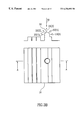
Turning first to FIG. 2, there is shown a schematic block diagram of a system (20) according to one embodiment of the invention. As shown, a source of light (21) illuminates a small region of an inspected wafer (22) that is secured to a known per se X-Y stage (not shown). The light source may be, for example, a conventional laser source. The incident light beam continuously scans the wafer in the X direction (arrow 23). At the end of each scan, the wafer is displaced in the Y direction arrow (24), under the control of said X-Y stage, and the wafer is rescanned in the X direction until the entire wafer has been scanned, all as known per se. Four evenly distributed dark field detectors 26, 27, 28 and 29 are placed adjacent to the peripheral edge of the wafer such that their respective fields of view substantially overlap to form the detection zone. The detection zone includes the illuminated region of the wafer, and due to the XY movement of the wafer relative to the detectors, the entire wafer will eventually pass through the detection zone.
Any incident light scattered in the direction of one or more of detectors 26, 27, 28 and/or 29 (e.g. photo multiplier or CCD) will be collected and converted into an electrical signal to be transmitted (typically in digital form) to an analyzer module 34 whose operation will be expounded upon in greater detail below.
Those versed in the art will readily appreciate that FIG. 2 illustrates only one out of many possible embodiments of the invention. Thus, by way of non-limiting example, when considering the detectors of the system, whereas in FIG. 2 four evenly distributed dark field detectors are shown, the invention is by no means bound by e.g. the number of detectors, the location of the detectors and/or their type. Two non-limiting dark field examples are shown also in FIGS. 9 and 10 below.
There follows a brief description of the so called scattered light attributes according to a specific embodiment of the invention which, as will be explained below, are used in the defect classification process. Attention is now directed to FIGS. 3A-B showing graphical representations of light scattering patterns as detected by respective, evenly distributed, dark field detectors in response to illuminating a particle (FIG. 3A) type defect. FIG. 3A shows a wafer (31) with a particle type defect adhered thereto (32) (shown in enlarged scale for the sake of clarity). A particle type defect is characterized by rising above the surface of the wafer. Due to the 3-dimensional (D) geometry of the particle and the irregular (non mirror like) surface thereof, the incident light beam is scattered in various directions as clearly shown in FIG. 3B. The latter illustrates, schematically a cross sectional side view of the wafer along A—A. Thus, light beam (35) that is incident on particle (32) is reflected in various directions (e.g. 36 (1) 36 (2) 36 (3) 36 (4) and 36 (5). Turning back to FIG. 3A, the reflected light is detected by the four evenly distributed detectors ((26) (27) (28) and (29)—see FIG. 2) and the intensity (in terms of gray level) as detected by each detector is illustrated graphically in respective 3D graphs (36)-(39) in FIG. 3A. Each graph represents an X-Y matrix of pixels and the detected intensity (Z) expressed in 8-bit gray level value. As expected, higher energy (represented as a higher gray level value) is sensed by those pixels in a detector receiving light scattered from the particle (e.g. 36′ in graph 36), compared to the energy sensed by those pixels which receive light reflected from the fault-free flat regions (e.g. 36″ in graph 36).
Since light is scattered from the 3D particle in all directions, a particle type defect is detected as a high energy level, sensed by most or all of the detectors). A pattern type defect, in contrast, does not substantially rise above the surface of the inspected wafer. Thus, as shown in FIG. 4, a pattern type defect will normally give rise to detected high energy in only a few of the detectors. Hence, by way of example, defect (41) has an irregular pattern as compared to that of neighboring members (42 and 43). The irregular pattern (41) has inclined edges (44) and (45) which, when illuminated by the incident beam, will scatter reflects light in directions (46) and (47), which is detected as a high intensity in regions (48) and (49) of detectors (26) and (28) respectively.
Whilst the specific pattern and particle examples depicted in FIGS. 3 and 4 are, of course, not binding and numerous others may be encountered in real life scenario, they serve, generally, for understanding the distinction between pattern and particle type defects.
As explained above, in order to classify defects to certain categories, it is necessary to identify pixels originating from a defect. There are known in the literature techniques for accomplishing preliminary defect detection and a typical, yet not exclusive, technique is explained with reference to FIG. 5 (see also U.S. Pat. No. 5,699,447 to Alumot)
Thus, FIG. 5 shows a graphic method for identifying pixels from a defect. The graph of FIG. 5 is constructed by plotting the gray level value of a pixel having (x,y) coordinates in a first die of an inspected wafer as a function of the gray level value of the pixel having the same (x,y) coordinates in a neighboring die. In the ideal case, (no defect), the two gray level values are equal and consequently all the points in Graph 5 lie on line (50). Put differently, the gray level value of the pixel in the first die (abscissa) is identical to the gray level value of the counterpart pixel in the neighboring die (ordinate). In reality, the points in the graph of FIG. 5 will be gathered around fine (50), and most of them will lie we the boundaries (52) and (53).
When a defect in a first die is encountered, a significant difference is detected between the gray level values of pixels originating from the defected region in first die and the gray level values of the counterpart pixels originating from the fault free region in a second die (for example, pixels 54, 55 and 56 that from part of a defect).
It should be noted that the graphic illustration of FIG. 5 is obtained by analyzing results obtained from one detector. As recalled, encountering defects in one detector does not necessarily imply that the same defect is encountered in the remaining detectors (see e.g. FIG. 4 where only two detectors detected the defect).
It should again be emphasized that the example of FIG. 5 is by no means binding and other techniques for detecting suspected defects are also feasible.
The following discussion will assist in understanding the specific scattered light attributes utilized for defect classification according to one embodiment of the invention, to wit:
Intensity: for all pixels classified by at least one detector as originating from a defect (or suspected of originating from a defect), sum the gray level values thereof so as to give rise to a total intensity value. Thus, for example, if 5 pixels in the first detector are classified as originating from a defect, and 6,8, and 5 pixels in respective second third and fourth detectors are, likewise, classified as originating from the defect, the total intensity value is calculated by summing the gray level values of the specified 24 pixels. Volume: the total number of pixels suspected of originating from defect in at least one detector. Thus, for example, if a given defect extends over 10 pixels in a first detector, 15 pixels in the second detector, 17 pixels in a third detector and none in the forth detector, the volume attribute is 10+15+17=42.
Linearity: this attribute grades how linear the array of defective pixels is in each detector. Thus, if all pixels suspected of originating from a defect lie (in a given detector) on a straight line, the linearity grade is 1. As the array of pixels deviates from a straight line, the linearity grade decreases
Asymmetry: this attribute grades the symmetry of the defect by comparing the intensities of the scattered light detected by pairs of radially opposite placed detectors.
Having described, in general, the scattered light attributes according to one embodiment of the invention, there follows a description, with reference to FIGS. 6 and 7, of a sequence of steps for performing defect classification.
It should be emphasized that after having detected pixels constituting a defect (e.g. by utilizing the technique of FIG. 5), the specified attributes are utilized for defect classification whilst the wafer is still under inspection (i.e. “on the fly).
Turning now to FIG. 6, a defect (61) is classified as Big (62) or Small (63) according to whether its volume attribute is smaller or larger than a threshold value B. In is specific example the threshold B is set to 16. For “Big” defects (62), a further analysis step which exploits a first threshold T1 (65) aims at distinguishing between a Particle type defect (66) and a Pattern type defect (67). As recalled, a particle has a substantially three-dimensional geometry, whereas a pattern has a substantially two-dimensional geometry. For a better understanding of the foregoing, attention is now directed to FIG. 1 showing a graphic representation of volume (abscissa) vs. intensity (ordinate) attributes. Distinguishing between a pattern and a particle is based on the observation that for a given volume attribute (i.e. number of pixels that constitute a defect), the intensity grade associated with a particle is, as a rule, higher than that associated with a pattern. This is due to the fact that particles tend to scatter the incident light in all directions and consequently, a high intensity is sensed in all detectors. In contrast, a pattern type defect of the same size (i.e. having the same volume value) tends to scatter the incident light in particular directions, so that only some of the detectors sense a high intensity (see e.g. FIG. 3A-B vs. 4). Thus, for a given defect size, a particle will give rise to a higher intensity attribute than a pattern.
This observation is clearly reflected in FIG. 7, where for “Big” volumes (i.e. exceeding the threshold B (64)), those defects lying above threshold T1 (65) are classified as particles whereas those residing below T1 are classified as patterns. Thus, for example, defects (71) and (72) both have the same volume grading 30, but respective intensity values of 2200 (below threshold T1) and 6800 (above threshold T1). Accordingly, the former is classified as a pattern and the latter a particle.
Reverting now to FIG. 6, T4 (68) provides an additional fine tuning tool. Thus, T4 can be placed between the abscissa and T1(designated T4″ in FIG. 6) or above T1(designated T4′ in FIG. 6). In the former option, T4″ assists in discerning between scratches and patterns. Thus, all the population of suspected defects that reside below T4″ is classified as patterns (70 in FIG. 6) whereas the population of patterns that reside between T4″ and T1 is subject to further analysis in order to distinguish between pattern and scratch. (see below). This decision criterion is based on the assumption that for a given volume, patterns will generate lower intensity than scratches and therefore all those population who generate low intensity for a given volume (i.e. they reside below T4″).
Now, The asymmetry and linearity attributes will assist in refined classification patterns into scratch type defects and pattern type defects. The underlying premise in distinguishing scratches from patterns is that scratches are linear whereas other pattern type defects are round. The linearity-asymmetry criterion is applied only to those populations that reside between T4″ and T1.
Bearing this general observation in mind, attention is now directed to FIG. 8, which will assist in clarifying the distinctions between scratches and patterns. The abscissa in FIG. 8 is the linear regression coefficient wherein 1 indicates perfect linear and 0 random scattering. In the graph of FIG. 8, the asymmetry values range from 0 to 0.7. The asymmetry value is obtained according to the following algorithmic expression: 1−(A+B/C+D)
where A, B are the intensities detected by respective members of a first pair of opposite detectors (e.g. 27 and 29 in FIG. 2) and C, D are the intensities detected by respective members of a second pair of opposite detectors (e.g. 26 and 28 in FIG. 2).
Thus, for example, defect (41) in FIG. 2 is asymmetric as it scatters light only in the directions of one pair of detectors and virtually does not reflect light in the direction of the other pair. The ratio A+B/C+D is thus small and the overall result 1−(A+B/C+D) is, obviously, close to 1.
Accordingly, the more asymmetry is the attribute of the defect the closer is the asymmetry grading to 1.
In FIG. 8, areas (81, 82 and 83) are characterized by high linear and asymmetric grading and therefore defects residing therein are classified as scratches (69 in FIG. 6). Defects residing in areas (84, 85 and 86), are characterized by low linearity and a high symmetric grading ((70) in FIG. 6) and are therefore classified as patterns.
The rest of the areas (87), (88) and 89) are equivocally classified as scratch or pattern.
It should be noted that various modifications may be applied. Thus, by way of a non limiting example, the thresholds which distinguish between the specified areas (0.2 and 0.5 in the ordinate) and (0.974 and 0.982 in the abscissa may be set to different values and, likewise, the number of areas may be changed, all as required and appropriate.
T4′ serves for fine tuning decision criteria between big particle and scratches. Thus, all the population of defects that reside above T4′ is classifies as big particles (since for a given volume they generate a very high intensity), whereas the population that reside between T1 and T4′ is send to the asymmetry-linearity decision phase for classifying the defects as scratch, big particle or not decided (i.e. scratch or big particle).
Turning now to small defects (63 in FIG. 6), due to their small geometry, it is difficult to apply the intensity/volume criteria used for big defects to discern between 3D particle) and 2D (pattern) defects. Thus, a second threshold T2 (73), serves for distinguishing between small particle (74) and small unknown (75). As before, 72 is determined empirically depending upon the particular application.
Now, the distinction between small pattern (74) and micro-scratch (76) obtained according to the asymmetric grading, i.e. symmetric defects are classified as small particle whereas asymmetric defects are classified as micro-scratches. Due to the small dimension of the defect, use of the linearity attribute to distinguish between micro scratches and small particles is unreliable and therefore not used.
Those versed in the art will readily appreciate that the definition of the scattered light attributes may be modified, one or more attributes may be deleted and/or others may be added, all as required and appropriate depending upon the particular application. Likewise, the utilization of scattered light attributes for classifying defects is by no means bound to the specific examples illustrated with reference to FIGS. 6 to 8. Put differently, the attributes may be utilized in a different manner for classifying the specified defects, one or more of the classifications may be modified, one or more classifications may be deleted and/or others may be added, all as required and appropriate. One, non-limiting, modification concerns utilization of at least one additional bright field detector (not shown). By this specific embodiment, the bright field detector contributes only to the volume attribute in that the number of pixels detected by the bright field detector (and which are suspected to originate from a defect) is summed to together with the counterpart numbers of pixels a contributed by the dark field detectors so as to constitute a volume value. Thus, the volume attribute will consist on the sum of pixels that form part of a defect in all the dark field detectors and in the bright field detector. The utilization of the bright field by this specific embodiment is based on that unlike dark field detectors, which sense energy reflected from only parts of the defect under question, bright field detector is placed above the defect and therefore has a clearer view of the entire defect or at least a major portion thereof.
By this specific example, the bright field detector does not contribute to the other attributes (intensity, linearity and asymmetry).
Another non-limiting modification is illustrated in reference to FIG. 9, where unlike FIG. 2, the illuminating beam (90) is incident on the wafer at an angle α substantially different than 90°. FIG. 10 illustrates yet another non limiting modification where the illuminating beam (100) is incident on the wafer at an angle α substantially different than 90°, and only two dark field detectors are utilized. Generally speaking, the exploitation of intensity, volume, asymmetry and linearity characteristics as generally illustrated and described with reference to FIG. 6 may be used in a similar manner also for the configurations of FIG. 9 and/or 10. This, however, is not obligatory.
It should be noted that designation of order of steps in the claims are done for convenience only.
The present invention has been described with a certain degree of particularity but it should be understood that various modifications and alterations may be made without departing from the scope or spirit of the invention as defined by the following claims:

Claims (41)

What is claimed is:
1. A method for on-the-fly automatic defect classification (ADC) in a scanned substrate, comprising:
(a) providing at least two spaced apart detectors;
(b) illuminating the scanned substrate so as to generate an illuminating spot incident on the substrate;
(c) collecting light scattered from the spot by at least two spaced apart detectors;
(d) analyzing said collected light so as to detect defects in said substrate; and
(e) classifying said defects into distinct defect types by analyzing scattered light volume attribute and at least one other attribute of said collected light;
wherein said step for analysis for classifying defects utilizing scattered light attributes includes at least one of the following attributes: scattered light intensity, scattered light linearity and scattered light asymmetry.
2. A system for on-the-fly automatic defect classification (ADC) in a inspected substrate, comprising:
(a) light source illuminating the inspected substrate;
(b) at least two spaced apart detectors situated to receive light scattered from the substrate and generating corresponding signals;
(c) a processor analyzing said signals so as to detect defects in said substrate; and
(d) a defect classifier analyzing scattered light volume attribute and at least one other attribute of said signals and classifying said defects into distinct defect types;
wherein said attributes correspond to at least one of the following attributes: scattered light intensity, scattered light linearity and reflected light asymmetry.
3. The system of claim 2, wherein said intensity and volume attributes are utilized for defining a first threshold; said classifier classifying said defects into particle type or pattern type per said first threshold.
4. The system of claim 3, wherein said intensity and volume attributes are further utilized for defining a second threshold; said classifier of utilizing said second threshold for classifying said pattern defects into pattern type defect or scratch type defect.
5. The system of claim 3, wherein said intensity and volume attributes are further utilized for defining a second threshold; said classifier utilizing said second threshold for classifying said particle defects into big particle type or scratch\particle type defect.
6. The system of claim 2, wherein said classifier utilizes said asymmetry and linearity attributes for classifying pattern type defect into scratch type defect or pattern type defect; said classifier further utilizes said asymmetry and linearity attributes for classifying particle type defect into particle type or scratch type defect.
7. A method for on-the-fly automatic defect classification (ADC) in a scanned substrate, comprising:
(a) providing at least two spaced apart detectors;
(b) illuminating the scanned substrate so as to generate an illuminating spot incident on the substrate;
(c) collecting light scattered from the spot by the at least two spaced apart detectors;
(d) analyzing said collected light so as to detect defects in said substrate and classifying said defects into distinct defect types; and
(e) classifying said defects into defect types by analyzing a scattered light volume attribute and at least one other attribute of said collecting light.
8. The method of claim 7, wherein said step (a) comprises providing at least four spaced apart dark field detectors.
9. The method of claim 8, wherein said step (a) comprises arranging said detectors such that each detector faces another detector located substantially opposite thereto.
10. The method of claim 8, wherein said step (a) comprises arranging said detectors in a substantially uniform distribution around the scanned substrate.
11. The method of claim 8, further comprising the steps of providing at least one additional bright field detector; reflected light being collected by said additional at least one bright field detector according to step (c) and said analysis, stipulated in said step (d), being applied to the reflected light collected by said additional at least one detector.
12. The method according to claim 8, wherein said step of classifying includes at least two of the following types: small particle, big particle; small pattern, big pattern; small scratch, big scratch.
13. The method of claim 7, wherein said step (a) comprises arranging said detectors such that the optical axis of each detector is at a grazing angle to the surface of the inspected substrate.
14. The method of claim 7, wherein said step (b) comprising illuminating the substrate such that said spot is incident on the substrate at a grazing angle to the substrate surface.
15. The method of claim 7, further comprising the steps of providing at least one additional bright field detector; reflected light being collected by said additional at least one bright field detector according to step (c) and said analysis, stipulated in said step (d), being applied to the reflected light collected by said additional at least one detector.
16. The method of claim 7, wherein said dark field detectors are arranged symmetrically about at least one axis.
17. The method of claim 7, wherein said steps for analyzing and classifying defects utilizes the scattered light volume attribute and comprises at least one of the following attributes: scattered light intensity, scattered light linearity and scattered light asymmetry.
18. The method according to claim 7, wherein said step of classifying includes at least two of the following types: small particle, big particle; small pattern, big pattern; small scratch, big scratch.
19. A system for on-the-fly automatic defect classification (ADC) in an inspected substrate, comprising:
(a) light source illuminating the inspected substrate;
(b) at least two spaced apart detectors situated to receive light scattered from the substrate and generating corresponding signals;
(c) a processor analyzing said signals so as to detect defects in said substrate; and
(d) a defect classifier analyzing a scattered light volume attribute and at least one other attribute of said signals and classifying said defects into distinct defect types.
20. The system of claim 19, wherein said at least two spaced apart detectors are arranged symmetrically about at least one axis.
21. The system of claim 20, wherein said classifier classifies said defects into at least two of the following types: small particle, big particle; small pattern, big pattern; small scratch, big scratch.
22. The system of claim 19, wherein said detectors are arranged such that each detector faces another detector located substantially opposite thereto.
23. The system of claim 19, wherein said detectors are arranged in a substantially uniform distribution around the scanned substrate.
24. The system of claim 19, wherein said detectors are arranged such that the optical axis of each detector is at a grazing angle to the surface of the inspected substrate.
25. The system of claim 19, wherein said light source illuminates the substrate at a grazing angle.
26. The system of claim 25, further comprising at least one bright field detector.
27. The system of claim 19, further comprising at least one bright field detector.
28. The system of claim 19, further comprising a first and a second thresholds, and wherein said defect classifier analyzes the signals with respect to said first threshold to differentiate between small and large defects, and analyzes the signals with respect to said second threshold to differentiate between pattern and particle defects.
29. The system of claim 19, wherein said at least one other attribute corresponds to at least one of the following attributes: scattered light intensity, scattered light linearity and reflected light asymmetry.
30. The system of claim 29, wherein said intensity and volume attributes are utilized for defining a first threshold; said classifier classifying said defects into particle type or pattern type per said first threshold.
31. The system of claim 30, wherein said intensity and volume attributes are further utilized for defining a second threshold; said classifier utilizing said second threshold for classifying said pattern defects into pattern type defect or scratch type defect.
32. The system of claim 30, wherein said intensity and volume attributes are further utilized for defining a second threshold; said classifier utilizing said second threshold for classifying said particle defects into big particle type or scratch\particle type defect.
33. The system of claim 29, wherein said classifier utilizes said asymmetry and linearity attributes for classifying pattern type defect into scratch type defect or pattern type defect; said classifier further utilizes said asymmetry and linearity attributes for classifying particle type defect into particle type or scratch type defect.
34. The system according to claim 19, wherein said classifier classifies said defects into at least two of the following types: small particle, big particle; small pattern, big pattern; small scratch, big scratch.
35. In a system for on-the-fly automatic defect classification (ADC) in a scanned wafer, a processor programmed to perform the steps comprising:
receiving signals from at least two spaced apart detectors, which signals are indicative of light scattered from the wafer and detected by said detectors; and
analyzing a scattered light volume and at least one other attribute of said signals so as to detect defects in said wafer and classifying said defects into distinct defect types.
36. An inspection system for inspecting substrates for defects, comprising:
a light source illuminating said substrate;
at least two detectors situated to detect light scattered from the substrate and generate at least a first and second inspection signals;
a comparator receiving and comparing said at least first and second inspection signals to at least a first and second reference signals, respectively, to detect defects in said substrate and identify defect locations;
a classifier receiving said at least said first and second inspection signals and analyzing a scattered light volume and at least one other attribute of said at least first and second inspection signals corresponding to said defect locations, and classifying said defects according to said attributes.
37. The inspection system of claim 36, wherein said at least one other attribute is selected from: intensity, linearity, and asymmetry.
38. The inspection system of claim 36, wherein intensity is obtained by summing intensities of said at least first and second inspection signals.
39. The inspection system of claim 36, wherein the scattered light volume is obtained by summing a number of pixels of said at least first and second inspection signals which correspond to a defect location.
40. The inspection system of claim 36, wherein linearity is obtained by determining alignment of pixels in said at least first and second inspection signals corresponding to defect locations.
41. The inspection system of claim 36, wherein asymmetry is obtained by comparing intensity levels of said at least first and second inspection signals corresponding to defect locations.
US09/104,226 1998-06-25 1998-06-25 On-the-fly automatic defect classification for substrates using signal attributes Expired - Lifetime US6256093B1 (en)

Priority Applications (7)

Application Number Priority Date Filing Date Title
US09/104,226 US6256093B1 (en) 1998-06-25 1998-06-25 On-the-fly automatic defect classification for substrates using signal attributes
JP2000556234A JP4846100B2 (en) 1998-06-25 1999-06-09 Wafer defect classification
KR1020007014727A KR100808716B1 (en) 1998-06-25 1999-06-09 A method and system for automatic defect classification
PCT/US1999/013082 WO1999067626A1 (en) 1998-06-25 1999-06-09 Wafer defect classification
EP99928543A EP1090284A1 (en) 1998-06-25 1999-06-09 Wafer defect classification
TW088110810A TW546754B (en) 1998-06-25 1999-07-16 On-the-fly automatic defect classification for substrates using signal attributes
JP2011184443A JP5572602B2 (en) 1998-06-25 2011-08-26 Wafer defect classification

Applications Claiming Priority (1)

Application Number Priority Date Filing Date Title
US09/104,226 US6256093B1 (en) 1998-06-25 1998-06-25 On-the-fly automatic defect classification for substrates using signal attributes

Publications (1)

Publication Number Publication Date
US6256093B1 true US6256093B1 (en) 2001-07-03

Family

ID=22299323

Family Applications (1)

Application Number Title Priority Date Filing Date
US09/104,226 Expired - Lifetime US6256093B1 (en) 1998-06-25 1998-06-25 On-the-fly automatic defect classification for substrates using signal attributes

Country Status (6)

Country Link
US (1) US6256093B1 (en)
EP (1) EP1090284A1 (en)
JP (2) JP4846100B2 (en)
KR (1) KR100808716B1 (en)
TW (1) TW546754B (en)
WO (1) WO1999067626A1 (en)

Cited By (57)

* Cited by examiner, † Cited by third party
Publication number Priority date Publication date Assignee Title
US20010033683A1 (en) * 2000-04-25 2001-10-25 Maki Tanaka Method of inspecting a pattern and an apparatus thereof and a method of processing a specimen
US6421122B2 (en) * 1998-11-30 2002-07-16 Hitachi, Ltd. Inspection method, apparatus and system for circuit pattern
US6515742B1 (en) 2000-11-28 2003-02-04 Memc Electronic Materials, Inc. Defect classification using scattered light intensities
US6587193B1 (en) * 1999-05-11 2003-07-01 Applied Materials, Inc. Inspection systems performing two-dimensional imaging with line light spot
US20030174878A1 (en) * 2002-03-12 2003-09-18 Evgeni Levin Muli-detector defect detection system and a method for detecting defects
US6628381B1 (en) * 2000-06-20 2003-09-30 Applied Materials, Inc. Optical inspection method and apparatus utilizing a collection angle design
US6657714B2 (en) * 2001-09-24 2003-12-02 Applied Materials, Inc. Defect detection with enhanced dynamic range
US20040030433A1 (en) * 2002-08-07 2004-02-12 Popp Robert L. Manufacturing information and alarming system and method
US6710868B2 (en) * 2002-05-22 2004-03-23 Applied Materials, Inc. Optical inspection system with dual detection heads
US6726319B1 (en) * 1999-10-14 2004-04-27 Sumitomo Mitsubishi Silicon Corporation Method for inspecting surface of semiconductor wafer
US6731384B2 (en) * 2000-10-10 2004-05-04 Hitachi, Ltd. Apparatus for detecting foreign particle and defect and the same method
US20040126962A1 (en) * 2002-12-25 2004-07-01 Szu-Tsun Ma [method of fabricating shallow trench isolation]
US20040129859A1 (en) * 2002-07-17 2004-07-08 Leica Microsystems Semiconductor Gmbh Method and apparatus for scanning a specimen using an optical imaging system
US20040136665A1 (en) * 2003-01-15 2004-07-15 Negevtech Ltd. Fiber optical illumination system
US20040146295A1 (en) * 2003-01-15 2004-07-29 Negevtech Ltd. System for detection of wafer defects
US20040233422A1 (en) * 2003-05-22 2004-11-25 Leica Microsystems Jena Gmbh Method and apparatus for high-resolution defect location and classification
US20050043841A1 (en) * 2002-08-07 2005-02-24 Kimberly-Clark Worldwide, Inc. Manufacturing information and troubleshooting system and method
US20050071029A1 (en) * 2003-09-30 2005-03-31 Noriaki Yamamoto Defect influence degree evaluation method and design support system
US20050128473A1 (en) * 1999-11-17 2005-06-16 Applied Materials, Inc. Method and apparatus for article inspection including speckle reduction
US6912304B1 (en) * 1999-08-02 2005-06-28 Applied Materials, Inc. Two-dimensional scatter plot technique for defect inspection
US20060007434A1 (en) * 2004-07-12 2006-01-12 Dov Furman Multi mode inspection method and apparatus
US20060012781A1 (en) * 2004-07-14 2006-01-19 Negevtech Ltd. Programmable spatial filter for wafer inspection
US20060115143A1 (en) * 2004-11-29 2006-06-01 Ditza Auerbach Method for filtering nuisance defects
US20060171846A1 (en) * 2005-01-10 2006-08-03 Marr David W M Microfluidic systems incorporating integrated optical waveguides
US20060171595A1 (en) * 2004-12-10 2006-08-03 Fumihiro Hasegawa Compressing a multivalue image with control of memory space requirement
US20060193506A1 (en) * 2005-02-28 2006-08-31 Negevtech Ltd. Method and apparatus for detecting defects in wafers including alignment of the wafer images so as to induce the same smear in all images
US20060193507A1 (en) * 2005-02-28 2006-08-31 Negevtech Ltd. Method and apparatus for detecting defects in wafers
US20060265145A1 (en) * 2004-09-30 2006-11-23 Patrick Huet Flexible hybrid defect classification for semiconductor manufacturing
US20070096044A1 (en) * 2003-10-01 2007-05-03 Sick Ivp Ab System and method of imaging the characteristics of an object
US20070146694A1 (en) * 2003-01-15 2007-06-28 Negevtech Ltd. Fiber optical illumination system
US20070171404A1 (en) * 2006-01-26 2007-07-26 Orbotech Ltd System and method for inspecting patterned devices having microscopic conductors
US7318902B2 (en) 2002-02-04 2008-01-15 Colorado School Of Mines Laminar flow-based separations of colloidal and cellular particles
US20080137073A1 (en) * 2006-11-28 2008-06-12 Negevtech, Ltd. Image Splitting in Optical Inspection Systems
US20080137074A1 (en) * 2006-11-28 2008-06-12 Negevtech, Ltd. Image Splitting in Optical Inspection Systems
US20090026387A1 (en) * 2007-07-03 2009-01-29 Colorado School Of Mines Optical-based cell deformability
US20090040525A1 (en) * 2007-08-10 2009-02-12 Azmi Kadkly Systems configured to inspect a wafer
US20090062828A1 (en) * 2007-09-04 2009-03-05 Colorado School Of Mines Magnetic field-based colloidal atherectomy
US20090110010A1 (en) * 2007-09-26 2009-04-30 Colorado School Of Mines Fiber-focused diode-bar optical trapping for microfluidic manipulation
US8031931B2 (en) 2006-04-24 2011-10-04 Applied Materials South East Asia Pte. Ltd. Printed fourier filtering in optical inspection tools
US20120261563A1 (en) * 2011-04-13 2012-10-18 Taiwan Semiconductor Manufacturing Company, Ltd. Contamination inspection
US8315453B2 (en) 2010-07-27 2012-11-20 Applied Materials Israel, Ltd. Defect classification with optimized purity
US20130038862A1 (en) * 2005-07-20 2013-02-14 Akira Hamamatsu Apparatus of inspecting defect in semiconductor and method of the same
US20130279796A1 (en) * 2012-04-20 2013-10-24 Applied Materials Israel Ltd. Classifier readiness and maintenance in automatic defect classification
US20140218723A1 (en) * 2000-03-08 2014-08-07 Hitachi High-Technologies Corporation Surface inspection apparatus and method thereof
US20140267227A1 (en) * 2013-03-14 2014-09-18 Ppg Industries Ohio, Inc. Systems and methods for texture analysis of a coated surface using multi-dimensional geometries
WO2015066384A1 (en) * 2013-10-30 2015-05-07 Applied Materials, Inc. Substrate processing system with particle scan and method of operation thereof
US9103800B2 (en) * 2004-12-19 2015-08-11 Kla-Tencor Corporation System with multiple scattered light collectors
US9487812B2 (en) 2012-02-17 2016-11-08 Colorado School Of Mines Optical alignment deformation spectroscopy
US20170082555A1 (en) * 2015-09-18 2017-03-23 Kla-Tencor Corporation Adaptive Automatic Defect Classification
US9715723B2 (en) 2012-04-19 2017-07-25 Applied Materials Israel Ltd Optimization of unknown defect rejection for automatic defect classification
US9885644B2 (en) 2006-01-10 2018-02-06 Colorado School Of Mines Dynamic viscoelasticity as a rapid single-cell biomarker
WO2018132321A1 (en) * 2017-01-10 2018-07-19 Kla-Tencor Corporation Diagnostic methods for the classifiers and the defects captured by optical tools
US10043264B2 (en) 2012-04-19 2018-08-07 Applied Materials Israel Ltd. Integration of automatic and manual defect classification
US10114368B2 (en) 2013-07-22 2018-10-30 Applied Materials Israel Ltd. Closed-loop automatic defect inspection and classification
US20190257876A1 (en) * 2018-02-21 2019-08-22 Asm Technology Singapore Pte Ltd System and method for detecting defects in an electronic device
US10722250B2 (en) 2007-09-04 2020-07-28 Colorado School Of Mines Magnetic-field driven colloidal microbots, methods for forming and using the same
US11237119B2 (en) 2017-01-10 2022-02-01 Kla-Tencor Corporation Diagnostic methods for the classifiers and the defects captured by optical tools

Families Citing this family (28)

* Cited by examiner, † Cited by third party
Publication number Priority date Publication date Assignee Title
US6999614B1 (en) 1999-11-29 2006-02-14 Kla-Tencor Corporation Power assisted automatic supervised classifier creation tool for semiconductor defects
US6925202B2 (en) 2001-03-20 2005-08-02 Synopsys, Inc. System and method of providing mask quality control
US6873720B2 (en) 2001-03-20 2005-03-29 Synopsys, Inc. System and method of providing mask defect printability analysis
US6650422B2 (en) * 2001-03-26 2003-11-18 Advanced Micro Devices, Inc. Scatterometry techniques to ascertain asymmetry profile of features and generate a feedback or feedforward process control data associated therewith
IL149588A (en) 2001-05-11 2007-07-24 Orbotech Ltd Image searching defect detector
US6721928B2 (en) 2001-07-26 2004-04-13 Numerical Technologies, Inc. Verification utilizing instance-based hierarchy management
US6560766B2 (en) 2001-07-26 2003-05-06 Numerical Technologies, Inc. Method and apparatus for analyzing a layout using an instance-based representation
US7014955B2 (en) 2001-08-28 2006-03-21 Synopsys, Inc. System and method for indentifying dummy features on a mask layer
US6976240B2 (en) 2001-11-14 2005-12-13 Synopsys Inc. Simulation using design geometry information
KR100970022B1 (en) * 2002-03-22 2010-07-16 어플라이드 머티리얼즈 이스라엘 리미티드 Dark field detection apparatus with traveling lens multi-beam scanner and a method thereof
US6809808B2 (en) * 2002-03-22 2004-10-26 Applied Materials, Inc. Wafer defect detection system with traveling lens multi-beam scanner
US7043071B2 (en) 2002-09-13 2006-05-09 Synopsys, Inc. Soft defect printability simulation and analysis for masks
EP1546691A1 (en) * 2002-09-30 2005-06-29 Applied Materials Israel Ltd. Inspection system with oblique viewing angle
JP2007501942A (en) 2003-05-19 2007-02-01 マイクロ−エプシロン・メステヒニク・ゲーエムベーハー・ウント・コンパニー・カー・ゲー Optical test method and optical test apparatus for optically controlling the quality of an object preferably having a circular edge
US7711177B2 (en) 2006-06-08 2010-05-04 Kla-Tencor Technologies Corp. Methods and systems for detecting defects on a specimen using a combination of bright field channel data and dark field channel data
US7728969B2 (en) 2006-12-05 2010-06-01 Kla-Tencor Technologies Corp. Methods and systems for identifying defect types on a wafer
KR101453033B1 (en) 2008-12-02 2014-10-23 주식회사 엘지실트론 Detection Method of Epitaxial Stacking Faults on Epitaxial Wafer
US8223327B2 (en) 2009-01-26 2012-07-17 Kla-Tencor Corp. Systems and methods for detecting defects on a wafer
US8605275B2 (en) 2009-01-26 2013-12-10 Kla-Tencor Corp. Detecting defects on a wafer
JP5506243B2 (en) * 2009-05-25 2014-05-28 株式会社日立製作所 Defect inspection equipment
US9595091B2 (en) * 2012-04-19 2017-03-14 Applied Materials Israel, Ltd. Defect classification using topographical attributes
US9008410B2 (en) 2013-03-13 2015-04-14 Kla-Tencor Corporation Single die inspection on a dark field inspection tool
JP5576526B2 (en) * 2013-04-01 2014-08-20 株式会社日立製作所 Surface inspection apparatus and method
US9535010B2 (en) * 2014-05-15 2017-01-03 Kla-Tencor Corp. Defect sampling for electron beam review based on defect attributes from optical inspection and optical review
JP5784796B2 (en) * 2014-06-02 2015-09-24 株式会社日立製作所 Surface inspection apparatus and method
US10234402B2 (en) * 2017-01-05 2019-03-19 Kla-Tencor Corporation Systems and methods for defect material classification
WO2018176370A1 (en) * 2017-03-31 2018-10-04 深圳配天智能技术研究院有限公司 Visual inspection system and method
CN110517970B (en) * 2019-08-29 2022-10-21 上海华力集成电路制造有限公司 Method for detecting defects of wafer back

Citations (14)

* Cited by examiner, † Cited by third party
Publication number Priority date Publication date Assignee Title
US4253768A (en) * 1978-08-09 1981-03-03 Westinghouse Electric Corp. Processing system for detection and the classification of flaws on metallic surfaces
US4587617A (en) * 1982-11-02 1986-05-06 Cambridge Instruments Limited Image inspection system for defect detection
US4626101A (en) * 1983-11-26 1986-12-02 Kabushiki Kaisha Toshiba Surface defect inspecting apparatus
JPH04152545A (en) 1990-10-17 1992-05-26 Hitachi Ltd Inspection method of foreign body
USRE33991E (en) * 1982-11-04 1992-07-14 Hitachi, Ltd. Foreign particle detecting method and apparatus
US5544256A (en) * 1993-10-22 1996-08-06 International Business Machines Corporation Automated defect classification system
WO1996039619A1 (en) 1995-06-06 1996-12-12 Kla Instruments Corporation Optical inspection of a specimen using multi-channel responses from the specimen
US5669447A (en) 1996-04-01 1997-09-23 Halliburton Energy Services, Inc. Methods for breaking viscosified fluids
WO1997046865A1 (en) 1996-06-04 1997-12-11 Tencor Instruments Optical scanning system for surface inspection
US5699447A (en) 1990-11-16 1997-12-16 Orbot Instruments Ltd. Two-phase optical inspection method and apparatus for defect detection
US5712701A (en) * 1995-03-06 1998-01-27 Ade Optical Systems Corporation Surface inspection system and method of inspecting surface of workpiece
US5798830A (en) * 1993-06-17 1998-08-25 Ultrapointe Corporation Method of establishing thresholds for image comparison
US5801965A (en) * 1993-12-28 1998-09-01 Hitachi, Ltd. Method and system for manufacturing semiconductor devices, and method and system for inspecting semiconductor devices
US5875027A (en) * 1997-03-28 1999-02-23 Hitachi Electronics Engineering Co. Sensitivity calibration disk for surface defect tester

Family Cites Families (3)

* Cited by examiner, † Cited by third party
Publication number Priority date Publication date Assignee Title
JPH08189896A (en) * 1995-01-11 1996-07-23 Matsushita Electric Ind Co Ltd Surface foreign matter inspecting device and surface foreign matter classifying method using the inspecting device
JP3523408B2 (en) * 1996-02-19 2004-04-26 東レエンジニアリング株式会社 Method and apparatus for measuring shape of uneven object
JP4001653B2 (en) * 1996-08-29 2007-10-31 ケーエルエー・インストルメンツ・コーポレーション Optical inspection of samples using multichannel response from the sample

Patent Citations (14)

* Cited by examiner, † Cited by third party
Publication number Priority date Publication date Assignee Title
US4253768A (en) * 1978-08-09 1981-03-03 Westinghouse Electric Corp. Processing system for detection and the classification of flaws on metallic surfaces
US4587617A (en) * 1982-11-02 1986-05-06 Cambridge Instruments Limited Image inspection system for defect detection
USRE33991E (en) * 1982-11-04 1992-07-14 Hitachi, Ltd. Foreign particle detecting method and apparatus
US4626101A (en) * 1983-11-26 1986-12-02 Kabushiki Kaisha Toshiba Surface defect inspecting apparatus
JPH04152545A (en) 1990-10-17 1992-05-26 Hitachi Ltd Inspection method of foreign body
US5699447A (en) 1990-11-16 1997-12-16 Orbot Instruments Ltd. Two-phase optical inspection method and apparatus for defect detection
US5798830A (en) * 1993-06-17 1998-08-25 Ultrapointe Corporation Method of establishing thresholds for image comparison
US5544256A (en) * 1993-10-22 1996-08-06 International Business Machines Corporation Automated defect classification system
US5801965A (en) * 1993-12-28 1998-09-01 Hitachi, Ltd. Method and system for manufacturing semiconductor devices, and method and system for inspecting semiconductor devices
US5712701A (en) * 1995-03-06 1998-01-27 Ade Optical Systems Corporation Surface inspection system and method of inspecting surface of workpiece
WO1996039619A1 (en) 1995-06-06 1996-12-12 Kla Instruments Corporation Optical inspection of a specimen using multi-channel responses from the specimen
US5669447A (en) 1996-04-01 1997-09-23 Halliburton Energy Services, Inc. Methods for breaking viscosified fluids
WO1997046865A1 (en) 1996-06-04 1997-12-11 Tencor Instruments Optical scanning system for surface inspection
US5875027A (en) * 1997-03-28 1999-02-23 Hitachi Electronics Engineering Co. Sensitivity calibration disk for surface defect tester

Non-Patent Citations (5)

* Cited by examiner, † Cited by third party
Title
PCT Written Opinion dated Mar. 23, 2000.
XP-002119842; Alumot et al., "Dual sensor technology for high-speed detection of 0.1 micron defects," Proceedings of the Spie-The International Society for Optical Engineering, vol. 1926, pp. 570-581; 1993.
XP-002119842; Alumot et al., "Dual sensor technology for high-speed detection of 0.1 micron defects," Proceedings of the Spie—The International Society for Optical Engineering, vol. 1926, pp. 570-581; 1993.
XP-002119843; Carmel et al., "New Directions in Process Control," Proceedings of the Spie-The International Society for Optical Engineering, vol. 2196, pp. 332-340; 1994.
XP-002119843; Carmel et al., "New Directions in Process Control," Proceedings of the Spie—The International Society for Optical Engineering, vol. 2196, pp. 332-340; 1994.

Cited By (109)

* Cited by examiner, † Cited by third party
Publication number Priority date Publication date Assignee Title
US6421122B2 (en) * 1998-11-30 2002-07-16 Hitachi, Ltd. Inspection method, apparatus and system for circuit pattern
US6493082B2 (en) * 1998-11-30 2002-12-10 Hitachi, Ltd. Inspection method, apparatus and system for circuit pattern
US6903821B2 (en) * 1998-11-30 2005-06-07 Hitachi, Ltd. Inspection method, apparatus and system for circuit pattern
US6587193B1 (en) * 1999-05-11 2003-07-01 Applied Materials, Inc. Inspection systems performing two-dimensional imaging with line light spot
US6912304B1 (en) * 1999-08-02 2005-06-28 Applied Materials, Inc. Two-dimensional scatter plot technique for defect inspection
US6726319B1 (en) * 1999-10-14 2004-04-27 Sumitomo Mitsubishi Silicon Corporation Method for inspecting surface of semiconductor wafer
US20050128473A1 (en) * 1999-11-17 2005-06-16 Applied Materials, Inc. Method and apparatus for article inspection including speckle reduction
US20140218723A1 (en) * 2000-03-08 2014-08-07 Hitachi High-Technologies Corporation Surface inspection apparatus and method thereof
US9551670B2 (en) * 2000-03-08 2017-01-24 Hitachi, Ltd. Surface inspection apparatus and method thereof
US20010033683A1 (en) * 2000-04-25 2001-10-25 Maki Tanaka Method of inspecting a pattern and an apparatus thereof and a method of processing a specimen
US7116816B2 (en) * 2000-04-25 2006-10-03 Hitachi, Ltd. Method of inspecting a pattern and an apparatus thereof and a method of processing a specimen
US6628381B1 (en) * 2000-06-20 2003-09-30 Applied Materials, Inc. Optical inspection method and apparatus utilizing a collection angle design
US6731384B2 (en) * 2000-10-10 2004-05-04 Hitachi, Ltd. Apparatus for detecting foreign particle and defect and the same method
US6515742B1 (en) 2000-11-28 2003-02-04 Memc Electronic Materials, Inc. Defect classification using scattered light intensities
US6657714B2 (en) * 2001-09-24 2003-12-02 Applied Materials, Inc. Defect detection with enhanced dynamic range
US6914670B1 (en) 2001-09-24 2005-07-05 Applied Materials, Inc. Defect detection with enhanced dynamic range
US7318902B2 (en) 2002-02-04 2008-01-15 Colorado School Of Mines Laminar flow-based separations of colloidal and cellular particles
US20090188795A1 (en) * 2002-02-04 2009-07-30 Colorado School Of Mines Cell sorting device and method of manufacturing the same
US20030174878A1 (en) * 2002-03-12 2003-09-18 Evgeni Levin Muli-detector defect detection system and a method for detecting defects
US7693323B2 (en) 2002-03-12 2010-04-06 Applied Materials, Inc. Multi-detector defect detection system and a method for detecting defects
WO2003078987A1 (en) 2002-03-12 2003-09-25 Applied Materials, Inc. Mutli-detector defect detection system and a method for detecting defects
US6710868B2 (en) * 2002-05-22 2004-03-23 Applied Materials, Inc. Optical inspection system with dual detection heads
US20040129859A1 (en) * 2002-07-17 2004-07-08 Leica Microsystems Semiconductor Gmbh Method and apparatus for scanning a specimen using an optical imaging system
US7247825B2 (en) 2002-07-17 2007-07-24 Vistec Semiconductor Systems Gmbh Method and apparatus for scanning a specimen using an optical imaging system
US6904330B2 (en) 2002-08-07 2005-06-07 Kimberly-Clark Worldwide, Inc. Manufacturing information and troubleshooting system and method
US20040030433A1 (en) * 2002-08-07 2004-02-12 Popp Robert L. Manufacturing information and alarming system and method
US20050043841A1 (en) * 2002-08-07 2005-02-24 Kimberly-Clark Worldwide, Inc. Manufacturing information and troubleshooting system and method
US7162319B2 (en) 2002-08-07 2007-01-09 Kimberly-Clark Worldwide, Inc. Manufacturing information and troubleshooting system and method
US7130709B2 (en) 2002-08-07 2006-10-31 Kimberly-Clark Worldwide, Inc. Manufacturing information and alarming system and method
US20040126962A1 (en) * 2002-12-25 2004-07-01 Szu-Tsun Ma [method of fabricating shallow trench isolation]
US20040146295A1 (en) * 2003-01-15 2004-07-29 Negevtech Ltd. System for detection of wafer defects
US7260298B2 (en) 2003-01-15 2007-08-21 Negevtech Ltd. Fiber optical illumination system
US20040136665A1 (en) * 2003-01-15 2004-07-15 Negevtech Ltd. Fiber optical illumination system
US7633041B2 (en) 2003-01-15 2009-12-15 Applied Materials South East Asia Pte, Ltd. Apparatus for determining optimum position of focus of an imaging system
US7525659B2 (en) 2003-01-15 2009-04-28 Negevtech Ltd. System for detection of water defects
US7843559B2 (en) 2003-01-15 2010-11-30 Applied Materials South East Asia Pte. Ltd. System for detection of wafer defects
US6892013B2 (en) 2003-01-15 2005-05-10 Negevtech Ltd. Fiber optical illumination system
US20050110987A1 (en) * 2003-01-15 2005-05-26 Negevtech Ltd. System for detection of wafer defects
US20060244958A1 (en) * 2003-01-15 2006-11-02 Negevtech Ltd. System for detection of wafer defects
US20060244956A1 (en) * 2003-01-15 2006-11-02 Negevtech Ltd. System for detection of wafer defects
US7477383B2 (en) 2003-01-15 2009-01-13 Negevtech Ltd. System for detection of wafer defects
US7961763B2 (en) 2003-01-15 2011-06-14 Applied Materials South East Asia Pte. Ltd. System for detection of wafer defects
US7486861B2 (en) 2003-01-15 2009-02-03 Negevtech Ltd. Fiber optical illumination system
US7180586B2 (en) 2003-01-15 2007-02-20 Negevtech Ltd. System for detection of wafer defects
US20050180707A1 (en) * 2003-01-15 2005-08-18 Negevtech Ltd. Fiber optical illumination system
US20070146694A1 (en) * 2003-01-15 2007-06-28 Negevtech Ltd. Fiber optical illumination system
US7242467B2 (en) * 2003-05-22 2007-07-10 Vistee Semiconductor Systems Jena Gmbh Method and apparatus for high-resolution defect location and classification
US20040233422A1 (en) * 2003-05-22 2004-11-25 Leica Microsystems Jena Gmbh Method and apparatus for high-resolution defect location and classification
US6973358B2 (en) * 2003-09-30 2005-12-06 Hitachi, Ltd. Defect influence degree evaluation method and design support system
US20050071029A1 (en) * 2003-09-30 2005-03-31 Noriaki Yamamoto Defect influence degree evaluation method and design support system
US20070096044A1 (en) * 2003-10-01 2007-05-03 Sick Ivp Ab System and method of imaging the characteristics of an object
US7502102B2 (en) * 2003-10-01 2009-03-10 Sick Ivp Ab System and method of imaging the characteristics of an object
US7274444B2 (en) 2004-07-12 2007-09-25 Negevtech Ltd. Multi mode inspection method and apparatus
US20060007434A1 (en) * 2004-07-12 2006-01-12 Dov Furman Multi mode inspection method and apparatus
US20060012781A1 (en) * 2004-07-14 2006-01-19 Negevtech Ltd. Programmable spatial filter for wafer inspection
US20060265145A1 (en) * 2004-09-30 2006-11-23 Patrick Huet Flexible hybrid defect classification for semiconductor manufacturing
US7142992B1 (en) 2004-09-30 2006-11-28 Kla-Tencor Technologies Corp. Flexible hybrid defect classification for semiconductor manufacturing
US7844100B2 (en) * 2004-11-29 2010-11-30 Applied Materials Israel, Ltd. Method for filtering nuisance defects
US20060115143A1 (en) * 2004-11-29 2006-06-01 Ditza Auerbach Method for filtering nuisance defects
US7639880B2 (en) * 2004-12-10 2009-12-29 Ricoh Company, Ltd. Compressing a multivalue image with control of memory space requirement
US20060171595A1 (en) * 2004-12-10 2006-08-03 Fumihiro Hasegawa Compressing a multivalue image with control of memory space requirement
US9103800B2 (en) * 2004-12-19 2015-08-11 Kla-Tencor Corporation System with multiple scattered light collectors
US20060171846A1 (en) * 2005-01-10 2006-08-03 Marr David W M Microfluidic systems incorporating integrated optical waveguides
US7804993B2 (en) 2005-02-28 2010-09-28 Applied Materials South East Asia Pte. Ltd. Method and apparatus for detecting defects in wafers including alignment of the wafer images so as to induce the same smear in all images
US20060193506A1 (en) * 2005-02-28 2006-08-31 Negevtech Ltd. Method and apparatus for detecting defects in wafers including alignment of the wafer images so as to induce the same smear in all images
US20060193507A1 (en) * 2005-02-28 2006-08-31 Negevtech Ltd. Method and apparatus for detecting defects in wafers
US7813541B2 (en) 2005-02-28 2010-10-12 Applied Materials South East Asia Pte. Ltd. Method and apparatus for detecting defects in wafers
US20130038862A1 (en) * 2005-07-20 2013-02-14 Akira Hamamatsu Apparatus of inspecting defect in semiconductor and method of the same
US8643834B2 (en) * 2005-07-20 2014-02-04 Hitachi High-Technologies Corporation Apparatus of inspecting defect in semiconductor and method of the same
US9885644B2 (en) 2006-01-10 2018-02-06 Colorado School Of Mines Dynamic viscoelasticity as a rapid single-cell biomarker
US7391510B2 (en) * 2006-01-26 2008-06-24 Orbotech Ltd System and method for inspecting patterned devices having microscopic conductors
US20070171404A1 (en) * 2006-01-26 2007-07-26 Orbotech Ltd System and method for inspecting patterned devices having microscopic conductors
CN101008622B (en) * 2006-01-26 2015-05-20 以色列商奥宝科技股份有限公司 System and method for inspecting patterned devices having microscopic conductors
US8031931B2 (en) 2006-04-24 2011-10-04 Applied Materials South East Asia Pte. Ltd. Printed fourier filtering in optical inspection tools
US20080137074A1 (en) * 2006-11-28 2008-06-12 Negevtech, Ltd. Image Splitting in Optical Inspection Systems
US20080137073A1 (en) * 2006-11-28 2008-06-12 Negevtech, Ltd. Image Splitting in Optical Inspection Systems
US7714998B2 (en) 2006-11-28 2010-05-11 Applied Materials South East Asia Pte. Ltd. Image splitting in optical inspection systems
US7719674B2 (en) 2006-11-28 2010-05-18 Applied Materials South East Asia Pte. Ltd. Image splitting in optical inspection systems
US8119976B2 (en) 2007-07-03 2012-02-21 Colorado School Of Mines Optical-based cell deformability
US20090026387A1 (en) * 2007-07-03 2009-01-29 Colorado School Of Mines Optical-based cell deformability
WO2009023154A3 (en) * 2007-08-10 2009-04-23 Kla Tencor Corp Systems configured to inspect a wafer
US20090040525A1 (en) * 2007-08-10 2009-02-12 Azmi Kadkly Systems configured to inspect a wafer
US7746459B2 (en) 2007-08-10 2010-06-29 Kla-Tencor Technologies Corp. Systems configured to inspect a wafer
WO2009023154A2 (en) * 2007-08-10 2009-02-19 Kla-Tencor Corporation Systems configured to inspect a wafer
US10722250B2 (en) 2007-09-04 2020-07-28 Colorado School Of Mines Magnetic-field driven colloidal microbots, methods for forming and using the same
US20090062828A1 (en) * 2007-09-04 2009-03-05 Colorado School Of Mines Magnetic field-based colloidal atherectomy
US9878326B2 (en) 2007-09-26 2018-01-30 Colorado School Of Mines Fiber-focused diode-bar optical trapping for microfluidic manipulation
US20090110010A1 (en) * 2007-09-26 2009-04-30 Colorado School Of Mines Fiber-focused diode-bar optical trapping for microfluidic manipulation
US8315453B2 (en) 2010-07-27 2012-11-20 Applied Materials Israel, Ltd. Defect classification with optimized purity
US8629407B2 (en) * 2011-04-13 2014-01-14 Taiwan Semiconductor Manufacturing Company, Ltd. Contamination inspection
US20120261563A1 (en) * 2011-04-13 2012-10-18 Taiwan Semiconductor Manufacturing Company, Ltd. Contamination inspection
US9487812B2 (en) 2012-02-17 2016-11-08 Colorado School Of Mines Optical alignment deformation spectroscopy
US9715723B2 (en) 2012-04-19 2017-07-25 Applied Materials Israel Ltd Optimization of unknown defect rejection for automatic defect classification
US10043264B2 (en) 2012-04-19 2018-08-07 Applied Materials Israel Ltd. Integration of automatic and manual defect classification
US9607233B2 (en) * 2012-04-20 2017-03-28 Applied Materials Israel Ltd. Classifier readiness and maintenance in automatic defect classification
US20130279796A1 (en) * 2012-04-20 2013-10-24 Applied Materials Israel Ltd. Classifier readiness and maintenance in automatic defect classification
US20140267227A1 (en) * 2013-03-14 2014-09-18 Ppg Industries Ohio, Inc. Systems and methods for texture analysis of a coated surface using multi-dimensional geometries
US9816862B2 (en) * 2013-03-14 2017-11-14 Ppg Industries Ohio, Inc. Systems and methods for texture analysis of a coated surface using multi-dimensional geometries
US10114368B2 (en) 2013-07-22 2018-10-30 Applied Materials Israel Ltd. Closed-loop automatic defect inspection and classification
US10901402B2 (en) 2013-07-22 2021-01-26 Applied Materials Israel, Ltd. Closed-loop automatic defect inspection and classification
WO2015066384A1 (en) * 2013-10-30 2015-05-07 Applied Materials, Inc. Substrate processing system with particle scan and method of operation thereof
CN108352339A (en) * 2015-09-18 2018-07-31 科磊股份有限公司 Adaptive automatic defect classification
US20170082555A1 (en) * 2015-09-18 2017-03-23 Kla-Tencor Corporation Adaptive Automatic Defect Classification
US10436720B2 (en) * 2015-09-18 2019-10-08 KLA-Tenfor Corp. Adaptive automatic defect classification
CN108352339B (en) * 2015-09-18 2022-11-08 科磊股份有限公司 Adaptive automatic defect classification
WO2018132321A1 (en) * 2017-01-10 2018-07-19 Kla-Tencor Corporation Diagnostic methods for the classifiers and the defects captured by optical tools
US11237119B2 (en) 2017-01-10 2022-02-01 Kla-Tencor Corporation Diagnostic methods for the classifiers and the defects captured by optical tools
TWI755468B (en) * 2017-01-10 2022-02-21 美商克萊譚克公司 Diagnostic methods for the classifiers and the defects captured by optical tools
US20190257876A1 (en) * 2018-02-21 2019-08-22 Asm Technology Singapore Pte Ltd System and method for detecting defects in an electronic device

Also Published As

Publication number Publication date
JP2002519632A (en) 2002-07-02
JP2012019224A (en) 2012-01-26
TW546754B (en) 2003-08-11
JP5572602B2 (en) 2014-08-13
KR100808716B1 (en) 2008-03-03
KR20010043996A (en) 2001-05-25
JP4846100B2 (en) 2011-12-28
EP1090284A1 (en) 2001-04-11
WO1999067626A1 (en) 1999-12-29

Similar Documents

Publication Publication Date Title
US6256093B1 (en) On-the-fly automatic defect classification for substrates using signal attributes
US8559000B2 (en) Method of inspecting a semiconductor device and an apparatus thereof
KR102153158B1 (en) Defect sampling for electron beam review based on defect attributes from optical inspection and optical review
KR101674698B1 (en) Detecting defects on a wafer
US7505619B2 (en) System and method for conducting adaptive fourier filtering to detect defects in dense logic areas of an inspection surface
US8660336B2 (en) Defect inspection system
KR101518801B1 (en) Computer-implemented methods, carrier media, and systems for selecting polarization settings for an inspection system
US7844100B2 (en) Method for filtering nuisance defects
US10677742B2 (en) Detecting die repeating programmed defects located in backgrounds with non-repeating features
CN107615469B (en) Evaluation method of semiconductor wafer
JP2001255278A (en) Surface inspection device and its method
US6798504B2 (en) Apparatus and method for inspecting surface of semiconductor wafer or the like
US7106432B1 (en) Surface inspection system and method for using photo detector array to detect defects in inspection surface
US7405817B2 (en) Method and apparatus for classifying defects of an object
JP3089079B2 (en) Circuit pattern defect inspection method
US6574359B1 (en) Method and apparatus for inspecting wafer defects
JPH08190633A (en) Defect judging method
KR100564871B1 (en) Inspecting method and apparatus for repeated micro-miniature patterns

Legal Events

Date Code Title Description
AS Assignment

Owner name: APPLIED MATERIALS, INC., CALIFORNIA

Free format text: ASSIGNMENT OF ASSIGNORS INTEREST;ASSIGNORS:RAVID, EREZ;HOLCMAN, IDO;MIKOLINSKY, VLADIMIR;REEL/FRAME:009469/0839;SIGNING DATES FROM 19980830 TO 19980902

AS Assignment

Owner name: APPLIED MATERIALS, INC., CALIFORNIA

Free format text: ASSIGNMENT OF ASSIGNORS INTEREST;ASSIGNOR:ORBOT INSTRUMENTS, LIMITED;REEL/FRAME:010885/0782

Effective date: 20000512

STCF Information on status: patent grant

Free format text: PATENTED CASE

FPAY Fee payment

Year of fee payment: 4

FPAY Fee payment

Year of fee payment: 8

FPAY Fee payment

Year of fee payment: 12