US6269022B1 - Threshold voltage setting circuit for reference memory cell and method for setting threshold voltage using the same - Google Patents
Threshold voltage setting circuit for reference memory cell and method for setting threshold voltage using the same Download PDFInfo
- Publication number
- US6269022B1 US6269022B1 US09/472,847 US47284799A US6269022B1 US 6269022 B1 US6269022 B1 US 6269022B1 US 47284799 A US47284799 A US 47284799A US 6269022 B1 US6269022 B1 US 6269022B1
- Authority
- US
- United States
- Prior art keywords
- memory cell
- reference memory
- current
- threshold voltage
- programming
- Prior art date
- Legal status (The legal status is an assumption and is not a legal conclusion. Google has not performed a legal analysis and makes no representation as to the accuracy of the status listed.)
- Expired - Lifetime
Links
Images


Classifications
-
- G—PHYSICS
- G11—INFORMATION STORAGE
- G11C—STATIC STORES
- G11C16/00—Erasable programmable read-only memories
- G11C16/02—Erasable programmable read-only memories electrically programmable
-
- G—PHYSICS
- G11—INFORMATION STORAGE
- G11C—STATIC STORES
- G11C29/00—Checking stores for correct operation ; Subsequent repair; Testing stores during standby or offline operation
- G11C29/02—Detection or location of defective auxiliary circuits, e.g. defective refresh counters
- G11C29/028—Detection or location of defective auxiliary circuits, e.g. defective refresh counters with adaption or trimming of parameters
-
- G—PHYSICS
- G11—INFORMATION STORAGE
- G11C—STATIC STORES
- G11C16/00—Erasable programmable read-only memories
- G11C16/02—Erasable programmable read-only memories electrically programmable
- G11C16/06—Auxiliary circuits, e.g. for writing into memory
- G11C16/34—Determination of programming status, e.g. threshold voltage, overprogramming or underprogramming, retention
- G11C16/3436—Arrangements for verifying correct programming or erasure
- G11C16/3454—Arrangements for verifying correct programming or for detecting overprogrammed cells
-
- G—PHYSICS
- G11—INFORMATION STORAGE
- G11C—STATIC STORES
- G11C29/00—Checking stores for correct operation ; Subsequent repair; Testing stores during standby or offline operation
- G11C29/04—Detection or location of defective memory elements, e.g. cell constructio details, timing of test signals
- G11C29/50—Marginal testing, e.g. race, voltage or current testing
- G11C29/50004—Marginal testing, e.g. race, voltage or current testing of threshold voltage
-
- G—PHYSICS
- G11—INFORMATION STORAGE
- G11C—STATIC STORES
- G11C16/00—Erasable programmable read-only memories
- G11C16/02—Erasable programmable read-only memories electrically programmable
- G11C16/04—Erasable programmable read-only memories electrically programmable using variable threshold transistors, e.g. FAMOS
-
- G—PHYSICS
- G11—INFORMATION STORAGE
- G11C—STATIC STORES
- G11C29/00—Checking stores for correct operation ; Subsequent repair; Testing stores during standby or offline operation
- G11C29/04—Detection or location of defective memory elements, e.g. cell constructio details, timing of test signals
- G11C29/50—Marginal testing, e.g. race, voltage or current testing
- G11C2029/5006—Current
Definitions
- the present invention relates to a semiconductor memory, and more particularly, to a threshold voltage setting circuit for a reference memory cell for immediate and accurate setting of a threshold voltage without time consumption; and a method for setting a threshold voltage using the same.
- FIG. 1 illustrates a circuitry system of a related art threshold voltage setting circuit for a reference memory cell.
- the related art threshold voltage setting circuit for a reference memory cell is provided with a plurality of memories 2 each having a gate terminal connected to a wordline 3 , and a drain terminal connected to a bitline. There is an inverter connected to an initial input terminal of each wordline 3 . There is a selection transistor 5 connected between a cascode device 6 and a drain terminal of respective memories 2 for connection of a column load device 7 to a pertinent memory 2 through the cascode device 6 . There is an inverter between a gate terminal and a source terminal of the cascode device 6 for inverting a signal from a source terminal and providing to the gate terminal.
- reference memory cell 9 each having a source, a drain, a control gate and a floating gate and connected to a reference column load device 12 through respective selection device 10 and cascode device 11 .
- an inverter between the gate terminal and the source terminal of the cascode device 11 for inverting a signal from the source terminal and providing to the gate terminal.
- a sense amplifier 8 having an SIN terminal with a voltage level of a contact node CN 1 of the column load device 7 and the cascode device 6 applied thereto and a RIN terminal with a voltage level of a contact node CN 2 of the column load device 12 and the cascode device 11 applied thereto.
- a switch SW between the contact node CN 1 and the SIN for controlling a path for transmitting a signal from the contact node CN 1 to the SIN terminal, and there is an NMOS transistor 16 for providing a signal to a pad 15 under the control of the controller 14 when the switch SW is closed.
- the sense amplifier 8 compares the signal to the SIN terminal to the signal to the RIN terminal.
- the floating gates of respective reference memory cells 9 are programmed to levels different from one another. In order to program the reference memory cells 9 to different levels, there is a voltage switch 13 for applying charge pulses to the reference memory cells 9 until respective memory cells 9 store target charge amounts. And, there is a controller 14 for controlling the voltage switch 13 the selection device 10 , the NMOS transistor and the switch SW.
- the foregoing related art circuit for setting a threshold voltage for a reference memory cell set the target threshold voltage accurately using a characteristic curve of a load connected to the bitline in the reference memory cell, and provides many program pulse combinations in programming the reference memory cell for minimizing a time period required for programming up to the target threshold voltages.
- a program pulse width is made large to permit a threshold voltage shift greater, and the program pulse width is made the smaller gradually as the threshold voltage approaches to a target value the more as the programing is repeated, for securing accuracy to the maximum and minimizing a time period required for reaching to the target threshold voltage.
- the controller 14 makes the program pulse combinations and sets up a reference for program verification.
- a program verification is made, for verifying reach of the threshold voltage to the target value. And, if not reached to the target, the programming/program verification is repeated until the threshold voltage of the reference memory cell is reached to the target threshold voltage.
- accurate verifying reference voltages are applied externally through the controller 14 , and a plurality of program pulse combinations are used for reducing an overall program time period.
- the related art circuit for setting a threshold voltage for a reference memory cell has the following problems.
- the verification of an injected charge amount required whenever the program pulses are provided to the reference memory cells causes a time period required for reaching to the target threshold voltage longer.
- the controller required for using a method, in which, a program pulse width is made large initially and the program pulse width is made the smaller as the threshold voltage approaches to a target value causes the operation complicated.
- the present invention is directed to a threshold voltage setting circuit for a reference memory cell for immediate and accurate setting of a threshold voltage without time consumption, and a method for setting a threshold voltage using the same that substantially obviates one or more of the problems due to limitations and disadvantages of the related art.
- the threshold voltage setting circuit for a reference memory cell includes a reference memory cell having a source, a drain, a floating gate and a control gate, a first power source for applying a voltage to the drain of the reference memory cell under the control of the current detector when the reference memory cell is programmed, a second power source for supplying a voltage to the control gate of the reference memory cell when the reference memory cell is programmed or read, a third current connected to the source of the reference memory cell, a switch connected to the drain of the reference memory cell for controlling a path for external measuring of a current flowing to the reference memory cell in response to a measuring signal, and a current detector connected between the first power source and the drain of the reference memory cell for providing a stop signal to the first and second power sources to stop the programming of the reference memory cell forcibly when a current to the reference memory cell, which is monitored during the programming of the reference memory cell in response to a program signal, is the same
- the method for setting a threshold voltage by using a circuit for setting a threshold voltage for a reference memory cell including the steps of (1) applying a voltage to the control gate for programming a selected unit reference memory cell in a reference memory cell unit, (2) closing a switch for measuring an initial current to the unit reference memory cell, (3) setting a first program stop reference current equal to, or slightly smaller than the initial current, (4) programming the selected unit reference memory cell by using the first program stop reference current according to an auto-verifying method, (5) fixing the voltage applied to the control gate of the selected unit reference memory cell and changing over to a read mode for measuring a current to the selected unit reference memory cell after the selected unit reference memory cell is programmed, (6) setting a target current by using a transconductance in a read mode at a target threshold voltage, (7) calculating a final program stop reference current by using a first program stop reference current, a target current, and a current measured in a read mode, (8) programming the selected unit reference memory cell by auto verifying
- FIG. 1 illustrates a circuitry system of a related art threshold voltage setting circuit for a reference memory cell
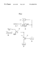
- FIG. 2 illustrates a circuitry system of a threshold voltage setting circuit for a reference memory cell in accordance with a preferred embodiment of the present invention
- FIG. 3 illustrates a concept for setting a threshold voltage for a reference memory cell in FIG. 2;
- FIG. 4 illustrates a flow chart showing a method for setting a threshold voltage for a reference memory cell in accordance with a preferred embodiment of the present invention.
- a circuit for setting a threshold voltage for a reference memory cell in accordance with a preferred embodiment of the present invention includes a reference memory cell 31 having a source, a drain, a floating gate and a control gate, a first power source VD 32 for supplying a program current to the reference memory cell 31 when the reference memory cell 31 is programmed, a second power source VC 33 for supplying voltage to the control gate of the reference memory cell 31 when the reference memory cell 31 is programmed or a current to the reference memory cell 31 is read, a third current VS 34 connected to the source of the reference memory cell 31 , a switch S 37 having one end connected to a drain of the reference memory cell 31 for controlling a path for external measuring of a current flowing to the reference memory cell 31 in response to a measuring signal, an external pad 36 connected to the other end of the switch 37 for direct external measuring of a current to the reference memory cell 31 , and a current detector 35 connected between the first power source 32 and a drain of the reference memory cell 31 for receiving a
- the second power source VC applies the same voltage when the reference memory cell is either programmed or read.
- the switch 37 is connected between the drain of the reference memory cell 31 and the external pad 36 for controlling connection between the drain of the reference memory cell 31 and the external pad 36 in response to a measure signal. This path is used for measuring the current to the reference memory cell 31 when the reference memory cell 31 is in operation.
- the control gate of the reference memory cell 31 has a VC C.OPR applied thereto, and the drain thereof has a voltage applied thereto, which is lower than the voltage used when the reference memory cell 31 is initialized.
- the drain has the voltage used when the reference memory cell 31 is initialized applied thereto as it is, the program operation is started no later than the reference memory cell 31 is put into operation, to ruin the threshold voltage of the reference memory cell 31 which is fixed with effort. Accordingly, when the reference memory cell 31 is put into operation actually after the reference memory cell 31 is initialized, approx. 1V is applied to the drain, the current to the reference memory cell 31 is measured through the external pad 36 while a voltage identical to the drain is applied from the external pad 36 .
- the current detector 35 is disabled using the program signal for excluding an influence from the VD voltage when the current to the reference memory cell 31 is measured externally, and leading the measuring current I MEASURE from the external pad 36 to flow only to the reference memory cell 31 .
- the V C.OPR is a gate voltage of the reference memory cell 31 used when the reference memory cell 31 is programmed or read, and identical to the operation voltage used actually after the reference memory cell 31 is initialized.
- the current detector 35 connected to the drain of the reference memory cell 31 controls program under the control of the program signal of the reference memory cell 31 .
- the current detector 35 Upon reception of a program signal PROGRAM of logic “0”, the current detector 35 is disabled, to cut the drain of the reference memory cell 31 from the first power source VD. This operation is used when the current to the reference memory cell 31 is measured or the reference memory cell 31 is erased externally. And, upon reception of a program signal PROGRAM of logic “1”, the first power source 31 VD is provided to the drain of the reference memory cell 31 , to start programming of the reference memory cell 31 . The current to the reference memory cell 31 is monitored on the same time with the program starting, until a moment the current to the reference memory cell 31 is equal to a preset reference stop current I STOP when a signal STOP is provided.
- the present invention basically has no problem of the related art which has a limitation of resolution caused by the pulse width(charge amount injected in one time).
- the present invention suggests use of auto-verify for setting a threshold voltage of a reference memory cell to a target value accurately only by two times of program, of which concept will be explained with reference to the attached drawings.
- the control gate voltage of the reference memory cell 31 may be the same both in programming and reading, the drain voltage of the same in reading should be substantially lower than in programming. If not so, i.e., if the voltages are the same, upon application of power for reading the current of the reference memory cell 31 , the reference memory cell 31 makes a programming operation right away, that makes the initialization meaningless. Thus, a difference between programming and reading of the reference memory cell 31 comes from a difference of voltages applied to the reference memory cell 31 in programming and reading.(the voltage in programming is as high as 4 ⁇ 6V and the voltage in reading is as low as 1V).
- a drain conductance g ds of the reference memory cell 31 is “0” ideally(an output resistance of the reference memory cell 31 is ⁇ ), with no current variation of the reference memory cell 31 caused by the drain voltage in a saturation region, it is possible that the reference memory cell reaches to the target current by one time of programming.
- the current in programming is greater than the current in reading as the g ds has a positive value.
- the present invention suggests calculation of a value for compensating a difference caused by g ds , by a first programming and using a result of the calculation in a second programming for setting the threshold voltage of the reference memory cell to the target value accurately by only two times of programming.
- the X-axis in FIG. 3 represents VC, a voltage applied to the control gate of the reference memory cell 31 , and the Y-axis represents a current I CELL to the reference memory cell 31 .
- V C.OPR in FIG. 3 denotes a voltage applied to the control gate of the reference memory cell 31 when the reference memory cell 31 is programmed or read
- V TH.TARGET denotes a target threshold voltage
- V TH.INIT denotes an initial threshold voltage of the reference memory cell 31 .
- V TH.M denotes a threshold voltage of the reference memory cell 31 when the reference memory cell 31 is programmed setting I PGM as a programming termination reference
- V C.M denotes a control gate voltage which leads a current by the threshold voltage of the first programming to be the same as the target current I REF
- I INIT on Y-axis denotes an initial current to the reference memory cell 31
- I PGM denotes a reference current for terminating the first programming of the reference memory cell 31
- I READ denotes a current measured after the first programming
- I FIN denotes a reference current for terminating the second programming of the reference memory cell 31
- I REF is a target current equal to the target threshold voltage of the reference memory cell 31 .
- a method for setting a threshold voltage for the reference memory cell of the present invention will be explained with reference to FIGS. 2, 3 and 4 .
- V C.OPR is applied to the second power source VC(S 100 ), a measuring signal Measure is enabled, and a current to the reference memory cell 31 is measured.
- a drain voltage to the reference memory cell 31 supplied from an external pad PAD 36 should be set to be operative at a read condition of the reference memory cell 31 .
- I INIT a point at which gm. READ a read mode gm at V TH.INIT and V C.OPR are met is measured(S 110 ).
- I PGM a reference current I STOP for stopping the first programming, is set equal to or slightly smaller than the I INIT (S 120 ).
- I PGM is set such that the threshold voltage after the first programming is to be around V TH.M which is in the middle of the V TH.INIT and the V TH.TARGET .
- I PGM may be set equal to I INIT , theoretically.
- the cell is programmed by auto-verify taking the set I PGM as I STOP (S 130 ).
- I STOP S 130
- FIG. 3 provided the programming is proceeded according the foregoing process, the programming will be stopped at a point V C.OPR and I PGM are met.
- a threshold voltage V TH.M after the programming can be obtained if an intersection of a line of gm of a program mode crossing the point V C.OPR and I PGM are met.
- V C.OPR and I PGM with X-axis is obtained.
- the current to the reference memory cell 31 is measured, while the V C.OPR , the control voltage to the reference memory cell 31 , is fixed and a mode is changed over to a measure mode, a point at which a read mode gm curve started from V TH.M meets with V C.OPR , i.e., I READ is measured.(S 140 ).
- I REF can be obtained at an intersection of the read mode gm curve started from the target threshold voltage with V C.OPR
- I FIN can be obtained at an intersection of the program mode gm curve started from the target threshold voltage with V C.OPR .
- the programming will terminate at an intersection of the V C.OPR and the I FIN . It can be known that an intersection of a program mode gm curve started from the intersection of the V C.OPR and the I FIN and X-axis are the V TH.TARGET .
- I PGM , I READ , I REF and V C.OPR are used in calculating and setting I FIN , which is I STOP .(S 150 ).
- the target threshold voltage can be set by one time of programming using the set I STOP .(S 160 ).
- the I FIN can be calculated according to the following equation.
- the gm a transconductance, is a current change of a reference memory cell 31 according to a voltage change of a control gate, i.e., as shown in FIG. 3, a value obtained by dividing an Y-axis change by an X-axis change. Therefore, a gm in a program mode and a read mode for V TH.M and V C.OPR can be obtained by equations (1) and (2) shown below, respectively.
- g m , PGM I PGM V C . OPR - V TH . M ( 1 )
- g m , READ I READ V C . OPR - V TH . M ( 2 )
- V C.M and V C.OPR can be expressed as equations (3) and (4).
- g m , PGM I PGM - I FIN V C . OPR - V C . M ( 3 )
- g m , READ I READ - I REF V C . OPR - V C . M ( 4 )
- a final target current I FIN can be obtained with easy by using I PGM which an initial program stop reference current, I REF which is the target current, and I READ which is a current measured in a read mode after the first program stop.
- I PGM initial program stop reference current
- I REF initial program stop reference current
- I READ which is a current measured in a read mode after the first program stop.
- an I FIN may be calculated by using the reference memory cell selected at the first time, which may then be used in common in initializing all the rest of reference memory cells.
- a number of programming required for entire reference memory cells will be a total number of cells to be initialized+1.
- I FIN may be calculated for all the reference memory cells respectively to use in initializing respective reference memory cells.
- a number of programming required for the initialization is a total number of the reference memory cells to be initialized ⁇ 2. In this instance, all the reference memory cells can be initialized, accurately.
- the threshold voltage setting circuit for a reference memory cell of the present invention and the method for setting a threshold voltage using the same have the following advantages.
- a threshold voltage of one reference memory cell can be set to a desired level from a condition the reference memory cell is operative actually by two times of programming, accurately and quickly.
Abstract
Description


Claims (8)
Applications Claiming Priority (2)
| Application Number | Priority Date | Filing Date | Title |
|---|---|---|---|
| KR1019990025469A KR100331847B1 (en) | 1999-06-29 | 1999-06-29 | Circuit for holding threshold voltage of reference memory cell and method for holding threshold voltage thereby |
| KR99-25469 | 1999-06-29 |
Publications (1)
| Publication Number | Publication Date |
|---|---|
| US6269022B1 true US6269022B1 (en) | 2001-07-31 |
Family
ID=19597229
Family Applications (1)
| Application Number | Title | Priority Date | Filing Date |
|---|---|---|---|
| US09/472,847 Expired - Lifetime US6269022B1 (en) | 1999-06-29 | 1999-12-28 | Threshold voltage setting circuit for reference memory cell and method for setting threshold voltage using the same |
Country Status (2)
| Country | Link |
|---|---|
| US (1) | US6269022B1 (en) |
| KR (1) | KR100331847B1 (en) |
Cited By (15)
| Publication number | Priority date | Publication date | Assignee | Title |
|---|---|---|---|---|
| US6449190B1 (en) * | 2001-01-17 | 2002-09-10 | Advanced Micro Devices, Inc. | Adaptive reference cells for a memory device |
| US6466480B2 (en) * | 2001-03-27 | 2002-10-15 | Micron Technology, Inc. | Method and apparatus for trimming non-volatile memory cells |
| US20040012997A1 (en) * | 2002-07-18 | 2004-01-22 | Mitsubishi Denki Kabushiki Kaisha | Nonvolatile semiconductor memory |
| US6788577B2 (en) * | 2001-12-28 | 2004-09-07 | Renesas Technology Corp. | Nonvolatile semiconductor memory |
| US20060239093A1 (en) * | 2005-04-12 | 2006-10-26 | Matsushita Electric Industrial Co., Ltd. | Semiconductor memory device |
| US20070036002A1 (en) * | 2002-12-26 | 2007-02-15 | Micron Technology, Inc. | Programming flash memories |
| US20080094892A1 (en) * | 2006-10-24 | 2008-04-24 | Fasoli Luca G | Method for protecting memory cells during programming |
| US7593249B2 (en) | 2006-10-24 | 2009-09-22 | Sandisk 3D Llc | Memory device for protecting memory cells during programming |
| US20090323392A1 (en) * | 2008-06-27 | 2009-12-31 | Fasoli Luca G | Smart detection circuit for writing to non-volatile storage |
| US20110261626A1 (en) * | 2010-04-22 | 2011-10-27 | Ki Seog Kim | Semiconductor memory device and method of operating the same |
| EP2487689A1 (en) | 2011-02-11 | 2012-08-15 | Freescale Semiconductor, Inc. Are | Digital method to obtain the I-V curves of NVM bitcells |
| CN103426478A (en) * | 2012-05-18 | 2013-12-04 | 北京兆易创新科技股份有限公司 | Read circuit of flash memory |
| US8711596B2 (en) | 2009-04-20 | 2014-04-29 | Sandisk 3D Llc | Memory system with data line switching scheme |
| US8913413B2 (en) | 2008-08-25 | 2014-12-16 | Sandisk 3D Llc | Memory system with sectional data lines |
| US20190006000A1 (en) * | 2016-09-16 | 2019-01-03 | Micron Technology, Inc. | Compensation for threshold voltage variation of memory cell components |
Families Citing this family (1)
| Publication number | Priority date | Publication date | Assignee | Title |
|---|---|---|---|---|
| CN113488097B (en) * | 2021-06-30 | 2024-03-29 | 恒烁半导体(合肥)股份有限公司 | Efficient reference current adjusting method, device and application for memory chip |
Citations (4)
| Publication number | Priority date | Publication date | Assignee | Title |
|---|---|---|---|---|
| US5608669A (en) | 1994-06-02 | 1997-03-04 | Intel Corporation | Fast internal reference cell trimming for flash EEPROM memory |
| US5966330A (en) * | 1998-04-30 | 1999-10-12 | Eon Silicon Devices, Inc. | Method and apparatus for measuring the threshold voltage of flash EEPROM memory cells being applied a variable control gate bias |
| US6128228A (en) * | 1998-11-13 | 2000-10-03 | Stmicroelectronics S.R.L. | Circuit for high-precision analog reading of nonvolatile memory cells, in particular analog or multilevel flash or EEPROM memory cells |
| US6169691B1 (en) * | 1998-09-15 | 2001-01-02 | Stmicroelectronics S.R.L. | Method for maintaining the memory content of non-volatile memory cells |
-
1999
- 1999-06-29 KR KR1019990025469A patent/KR100331847B1/en not_active IP Right Cessation
- 1999-12-28 US US09/472,847 patent/US6269022B1/en not_active Expired - Lifetime
Patent Citations (4)
| Publication number | Priority date | Publication date | Assignee | Title |
|---|---|---|---|---|
| US5608669A (en) | 1994-06-02 | 1997-03-04 | Intel Corporation | Fast internal reference cell trimming for flash EEPROM memory |
| US5966330A (en) * | 1998-04-30 | 1999-10-12 | Eon Silicon Devices, Inc. | Method and apparatus for measuring the threshold voltage of flash EEPROM memory cells being applied a variable control gate bias |
| US6169691B1 (en) * | 1998-09-15 | 2001-01-02 | Stmicroelectronics S.R.L. | Method for maintaining the memory content of non-volatile memory cells |
| US6128228A (en) * | 1998-11-13 | 2000-10-03 | Stmicroelectronics S.R.L. | Circuit for high-precision analog reading of nonvolatile memory cells, in particular analog or multilevel flash or EEPROM memory cells |
Cited By (29)
| Publication number | Priority date | Publication date | Assignee | Title |
|---|---|---|---|---|
| US6449190B1 (en) * | 2001-01-17 | 2002-09-10 | Advanced Micro Devices, Inc. | Adaptive reference cells for a memory device |
| US6992931B2 (en) | 2001-03-27 | 2006-01-31 | Micron Technology, Inc. | System for trimming non-volatile memory cells |
| US6466480B2 (en) * | 2001-03-27 | 2002-10-15 | Micron Technology, Inc. | Method and apparatus for trimming non-volatile memory cells |
| US20030007383A1 (en) * | 2001-03-27 | 2003-01-09 | Micron Technology, Inc. | Memory device with non-volatile reference memory cell trimming capabilities |
| US7120060B2 (en) | 2001-03-27 | 2006-10-10 | Micron Technology, Inc. | Memory device with non-volatile reference memory cell trimming capabilities |
| US20050002239A1 (en) * | 2001-03-27 | 2005-01-06 | Micron Technology, Inc. | Memory device with non-volatile reference memory cell trimming capabilities |
| US6788577B2 (en) * | 2001-12-28 | 2004-09-07 | Renesas Technology Corp. | Nonvolatile semiconductor memory |
| US20040012997A1 (en) * | 2002-07-18 | 2004-01-22 | Mitsubishi Denki Kabushiki Kaisha | Nonvolatile semiconductor memory |
| US6735119B2 (en) | 2002-07-18 | 2004-05-11 | Renesas Technology Corp. | Nonvolatile semiconductor memory |
| US20070036002A1 (en) * | 2002-12-26 | 2007-02-15 | Micron Technology, Inc. | Programming flash memories |
| US7355894B2 (en) * | 2002-12-26 | 2008-04-08 | Micron Technology, Inc. | Programming flash memories |
| US20060239093A1 (en) * | 2005-04-12 | 2006-10-26 | Matsushita Electric Industrial Co., Ltd. | Semiconductor memory device |
| US7330374B2 (en) | 2005-04-12 | 2008-02-12 | Matsushita Electric Industrial Co., Ltd. | Nonvolatile semiconductor memory device, such as an EEPROM or a flash memory, with reference cells |
| US7589989B2 (en) * | 2006-10-24 | 2009-09-15 | Sandisk 3D Llc | Method for protecting memory cells during programming |
| US7593249B2 (en) | 2006-10-24 | 2009-09-22 | Sandisk 3D Llc | Memory device for protecting memory cells during programming |
| US20080094892A1 (en) * | 2006-10-24 | 2008-04-24 | Fasoli Luca G | Method for protecting memory cells during programming |
| US20090323392A1 (en) * | 2008-06-27 | 2009-12-31 | Fasoli Luca G | Smart detection circuit for writing to non-volatile storage |
| US8111539B2 (en) * | 2008-06-27 | 2012-02-07 | Sandisk 3D Llc | Smart detection circuit for writing to non-volatile storage |
| KR101568327B1 (en) | 2008-06-27 | 2015-11-12 | 쌘디스크 3디 엘엘씨 | Simultaneous write and verify in a non-volatile storage |
| US8913413B2 (en) | 2008-08-25 | 2014-12-16 | Sandisk 3D Llc | Memory system with sectional data lines |
| US8711596B2 (en) | 2009-04-20 | 2014-04-29 | Sandisk 3D Llc | Memory system with data line switching scheme |
| US20110261626A1 (en) * | 2010-04-22 | 2011-10-27 | Ki Seog Kim | Semiconductor memory device and method of operating the same |
| US8976598B2 (en) * | 2010-04-22 | 2015-03-10 | Hynix Semiconductor Inc. | Semiconductor memory device and method of operating the same |
| US8427877B2 (en) | 2011-02-11 | 2013-04-23 | Freescale Semiconductor, Inc. | Digital method to obtain the I-V curves of NVM bitcells |
| EP2487689A1 (en) | 2011-02-11 | 2012-08-15 | Freescale Semiconductor, Inc. Are | Digital method to obtain the I-V curves of NVM bitcells |
| CN103426478A (en) * | 2012-05-18 | 2013-12-04 | 北京兆易创新科技股份有限公司 | Read circuit of flash memory |
| CN103426478B (en) * | 2012-05-18 | 2016-12-21 | 北京兆易创新科技股份有限公司 | A kind of reading circuit of flash memory |
| US20190006000A1 (en) * | 2016-09-16 | 2019-01-03 | Micron Technology, Inc. | Compensation for threshold voltage variation of memory cell components |
| US10607675B2 (en) * | 2016-09-16 | 2020-03-31 | Micron Technology, Inc. | Compensation for threshold voltage variation of memory cell components |
Also Published As
| Publication number | Publication date |
|---|---|
| KR100331847B1 (en) | 2002-04-09 |
| KR20010004755A (en) | 2001-01-15 |
Similar Documents
| Publication | Publication Date | Title |
|---|---|---|
| US6269022B1 (en) | Threshold voltage setting circuit for reference memory cell and method for setting threshold voltage using the same | |
| US6078518A (en) | Apparatus and method for reading state of multistate non-volatile memory cells | |
| US5912838A (en) | Apparatus for reading state of multistate non-volatile memory cells | |
| US5784314A (en) | Method for setting the threshold voltage of a reference memory cell | |
| US6163484A (en) | Non-volatile semiconductor storage device having improved program/erase/over erase verify | |
| US6222768B1 (en) | Auto adjusting window placement scheme for an NROM virtual ground array | |
| US5966330A (en) | Method and apparatus for measuring the threshold voltage of flash EEPROM memory cells being applied a variable control gate bias | |
| US20020176281A1 (en) | Sensing scheme of flash eeprom | |
| US7269092B1 (en) | Circuitry and device for generating and adjusting selected word line voltage | |
| JPH097383A (en) | Nonvolatile semiconductor memory device and its word-line driving method | |
| EP0852848A1 (en) | Programmable logic device with configurable power supply | |
| US6101125A (en) | Electrically programmable memory and method of programming | |
| US6052310A (en) | Method for tightening erase threshold voltage distribution in flash electrically erasable programmable read-only memory (EEPROM) | |
| JPH11328987A (en) | Nonvolatile semiconductor memory device | |
| EP1543526B1 (en) | Method of recovering overerased bits in a memory device | |
| US7564714B2 (en) | Flash memory device and method of controlling program voltage | |
| JP2004039075A (en) | Nonvolatile semiconductor memory device | |
| JPH09282895A (en) | Nonvolatile semiconductor storage device and verifying method | |
| US7518930B2 (en) | Method for generating and adjusting selected word line voltage | |
| US6278634B1 (en) | Reference memory cell initialization circuit and method | |
| US6987703B2 (en) | Nonvolatile semiconductor storage device and write time determining method therefor | |
| JPH11297086A (en) | Nonvolatile semiconductor memory, integrated circuit including the same and method of adjusting write time of memory | |
| JP3943790B2 (en) | Negative potential detection circuit and semiconductor memory device provided with the negative potential detection circuit | |
| JPH10188587A (en) | Programmable reference voltage source for analog memory | |
| KR100443792B1 (en) | Circuit for programming a flash EEPROM and method of programming a flash EEPROM using the same |
Legal Events
| Date | Code | Title | Description |
|---|---|---|---|
| AS | Assignment |
Owner name: HYUNDAI ELECTRONICS INDUSTRIES CO., LTD., KOREA, R Free format text: ASSIGNMENT OF ASSIGNORS INTEREST;ASSIGNOR:RA, KYEONG MAN;REEL/FRAME:010507/0997 Effective date: 19991206 |
|
| STCF | Information on status: patent grant |
Free format text: PATENTED CASE |
|
| FEPP | Fee payment procedure |
Free format text: PAYOR NUMBER ASSIGNED (ORIGINAL EVENT CODE: ASPN); ENTITY STATUS OF PATENT OWNER: LARGE ENTITY |
|
| FPAY | Fee payment |
Year of fee payment: 4 |
|
| FPAY | Fee payment |
Year of fee payment: 8 |
|
| FEPP | Fee payment procedure |
Free format text: PAYER NUMBER DE-ASSIGNED (ORIGINAL EVENT CODE: RMPN); ENTITY STATUS OF PATENT OWNER: LARGE ENTITY Free format text: PAYOR NUMBER ASSIGNED (ORIGINAL EVENT CODE: ASPN); ENTITY STATUS OF PATENT OWNER: LARGE ENTITY |
|
| FPAY | Fee payment |
Year of fee payment: 12 |
|
| AS | Assignment |
Owner name: FIDELIX CO., LTD., KOREA, REPUBLIC OF Free format text: ASSIGNMENT OF ASSIGNORS INTEREST;ASSIGNOR:SK HYNIX INC.;REEL/FRAME:030086/0328 Effective date: 20130307 Owner name: SK HYNIX INC., KOREA, REPUBLIC OF Free format text: CHANGE OF NAME;ASSIGNOR:HYUNDAI ELECTRONICS INDUSTRIES CO., LTD.;REEL/FRAME:030088/0593 Effective date: 20120323 |
|
| AS | Assignment |
Owner name: DOSILICON CO., LTD., CHINA Free format text: ASSIGNMENT OF ASSIGNORS INTEREST;ASSIGNOR:FIDELIX CO., LTD.;REEL/FRAME:042244/0073 Effective date: 20170412 |