US6270619B1 - Treatment device, laser annealing device, manufacturing apparatus, and manufacturing apparatus for flat display device - Google Patents
Treatment device, laser annealing device, manufacturing apparatus, and manufacturing apparatus for flat display device Download PDFInfo
- Publication number
- US6270619B1 US6270619B1 US09/229,581 US22958199A US6270619B1 US 6270619 B1 US6270619 B1 US 6270619B1 US 22958199 A US22958199 A US 22958199A US 6270619 B1 US6270619 B1 US 6270619B1
- Authority
- US
- United States
- Prior art keywords
- section
- treatment
- substrate
- stage
- washing
- Prior art date
- Legal status (The legal status is an assumption and is not a legal conclusion. Google has not performed a legal analysis and makes no representation as to the accuracy of the status listed.)
- Expired - Lifetime
Links
- 238000011282 treatment Methods 0.000 title claims abstract description 270
- 238000004519 manufacturing process Methods 0.000 title claims abstract description 64
- 238000005224 laser annealing Methods 0.000 title claims description 57
- 239000000758 substrate Substances 0.000 claims abstract description 351
- 238000005406 washing Methods 0.000 claims abstract description 142
- 238000012546 transfer Methods 0.000 claims abstract description 106
- 239000010408 film Substances 0.000 claims description 108
- 238000000137 annealing Methods 0.000 claims description 76
- 239000012298 atmosphere Substances 0.000 claims description 58
- 238000011068 loading method Methods 0.000 claims description 28
- 230000007246 mechanism Effects 0.000 claims description 20
- 239000010409 thin film Substances 0.000 claims description 11
- 229910021419 crystalline silicon Inorganic materials 0.000 claims description 8
- 230000003287 optical effect Effects 0.000 claims description 8
- 238000005229 chemical vapour deposition Methods 0.000 claims description 6
- 230000008602 contraction Effects 0.000 claims 2
- 239000011521 glass Substances 0.000 abstract description 128
- 238000000034 method Methods 0.000 description 31
- 230000008569 process Effects 0.000 description 28
- 239000007789 gas Substances 0.000 description 25
- 239000012530 fluid Substances 0.000 description 24
- 238000001312 dry etching Methods 0.000 description 18
- 150000002500 ions Chemical class 0.000 description 17
- QVGXLLKOCUKJST-UHFFFAOYSA-N atomic oxygen Chemical compound [O] QVGXLLKOCUKJST-UHFFFAOYSA-N 0.000 description 16
- 239000001301 oxygen Substances 0.000 description 16
- 229910052760 oxygen Inorganic materials 0.000 description 16
- 238000010438 heat treatment Methods 0.000 description 14
- 238000010276 construction Methods 0.000 description 13
- 238000001039 wet etching Methods 0.000 description 13
- 239000010410 layer Substances 0.000 description 10
- 239000002245 particle Substances 0.000 description 10
- VYPSYNLAJGMNEJ-UHFFFAOYSA-N Silicium dioxide Chemical compound O=[Si]=O VYPSYNLAJGMNEJ-UHFFFAOYSA-N 0.000 description 7
- 229910021417 amorphous silicon Inorganic materials 0.000 description 7
- 238000001514 detection method Methods 0.000 description 7
- 238000001259 photo etching Methods 0.000 description 7
- 238000002203 pretreatment Methods 0.000 description 7
- IJGRMHOSHXDMSA-UHFFFAOYSA-N Atomic nitrogen Chemical compound N#N IJGRMHOSHXDMSA-UHFFFAOYSA-N 0.000 description 6
- 239000012535 impurity Substances 0.000 description 6
- 239000004973 liquid crystal related substance Substances 0.000 description 6
- 229910052751 metal Inorganic materials 0.000 description 6
- 239000002184 metal Substances 0.000 description 6
- 239000012299 nitrogen atmosphere Substances 0.000 description 6
- ZOXJGFHDIHLPTG-UHFFFAOYSA-N Boron Chemical compound [B] ZOXJGFHDIHLPTG-UHFFFAOYSA-N 0.000 description 5
- OAICVXFJPJFONN-UHFFFAOYSA-N Phosphorus Chemical compound [P] OAICVXFJPJFONN-UHFFFAOYSA-N 0.000 description 5
- 229910052796 boron Inorganic materials 0.000 description 5
- 239000011229 interlayer Substances 0.000 description 5
- 230000004048 modification Effects 0.000 description 5
- 238000012986 modification Methods 0.000 description 5
- 229910052698 phosphorus Inorganic materials 0.000 description 5
- 239000011574 phosphorus Substances 0.000 description 5
- 229910021420 polycrystalline silicon Inorganic materials 0.000 description 5
- 229910004205 SiNX Inorganic materials 0.000 description 4
- 238000005530 etching Methods 0.000 description 4
- 239000011435 rock Substances 0.000 description 4
- 230000032258 transport Effects 0.000 description 4
- 229910052799 carbon Inorganic materials 0.000 description 3
- 239000003795 chemical substances by application Substances 0.000 description 3
- 229910052681 coesite Inorganic materials 0.000 description 3
- 238000011109 contamination Methods 0.000 description 3
- 238000012937 correction Methods 0.000 description 3
- 229910052906 cristobalite Inorganic materials 0.000 description 3
- 239000013078 crystal Substances 0.000 description 3
- 230000000694 effects Effects 0.000 description 3
- 239000000377 silicon dioxide Substances 0.000 description 3
- 229910052814 silicon oxide Inorganic materials 0.000 description 3
- 229910052682 stishovite Inorganic materials 0.000 description 3
- 229910052905 tridymite Inorganic materials 0.000 description 3
- 229910000838 Al alloy Inorganic materials 0.000 description 2
- XKRFYHLGVUSROY-UHFFFAOYSA-N Argon Chemical compound [Ar] XKRFYHLGVUSROY-UHFFFAOYSA-N 0.000 description 2
- XUIMIQQOPSSXEZ-UHFFFAOYSA-N Silicon Chemical compound [Si] XUIMIQQOPSSXEZ-UHFFFAOYSA-N 0.000 description 2
- 229910052782 aluminium Inorganic materials 0.000 description 2
- XAGFODPZIPBFFR-UHFFFAOYSA-N aluminium Chemical compound [Al] XAGFODPZIPBFFR-UHFFFAOYSA-N 0.000 description 2
- 230000015572 biosynthetic process Effects 0.000 description 2
- 238000000576 coating method Methods 0.000 description 2
- 238000001035 drying Methods 0.000 description 2
- 230000002708 enhancing effect Effects 0.000 description 2
- -1 etc. Substances 0.000 description 2
- 238000009434 installation Methods 0.000 description 2
- 229910052757 nitrogen Inorganic materials 0.000 description 2
- 230000003647 oxidation Effects 0.000 description 2
- 238000007254 oxidation reaction Methods 0.000 description 2
- 230000001681 protective effect Effects 0.000 description 2
- 238000000926 separation method Methods 0.000 description 2
- 229910052710 silicon Inorganic materials 0.000 description 2
- 239000010703 silicon Substances 0.000 description 2
- XLYOFNOQVPJJNP-UHFFFAOYSA-N water Substances O XLYOFNOQVPJJNP-UHFFFAOYSA-N 0.000 description 2
- BOTDANWDWHJENH-UHFFFAOYSA-N Tetraethyl orthosilicate Chemical compound CCO[Si](OCC)(OCC)OCC BOTDANWDWHJENH-UHFFFAOYSA-N 0.000 description 1
- 230000002411 adverse Effects 0.000 description 1
- 229910052786 argon Inorganic materials 0.000 description 1
- 238000000861 blow drying Methods 0.000 description 1
- 238000010586 diagram Methods 0.000 description 1
- 229910001873 dinitrogen Inorganic materials 0.000 description 1
- 230000006872 improvement Effects 0.000 description 1
- 239000011261 inert gas Substances 0.000 description 1
- 238000007726 management method Methods 0.000 description 1
- 239000000463 material Substances 0.000 description 1
- 239000011159 matrix material Substances 0.000 description 1
- 238000005259 measurement Methods 0.000 description 1
- 230000000149 penetrating effect Effects 0.000 description 1
- 238000012545 processing Methods 0.000 description 1
- 230000004044 response Effects 0.000 description 1
- 239000004065 semiconductor Substances 0.000 description 1
- 230000001235 sensitizing effect Effects 0.000 description 1
- 238000004904 shortening Methods 0.000 description 1
- 230000000087 stabilizing effect Effects 0.000 description 1
Images


Classifications
-
- G—PHYSICS
- G02—OPTICS
- G02F—OPTICAL DEVICES OR ARRANGEMENTS FOR THE CONTROL OF LIGHT BY MODIFICATION OF THE OPTICAL PROPERTIES OF THE MEDIA OF THE ELEMENTS INVOLVED THEREIN; NON-LINEAR OPTICS; FREQUENCY-CHANGING OF LIGHT; OPTICAL LOGIC ELEMENTS; OPTICAL ANALOGUE/DIGITAL CONVERTERS
- G02F1/00—Devices or arrangements for the control of the intensity, colour, phase, polarisation or direction of light arriving from an independent light source, e.g. switching, gating or modulating; Non-linear optics
- G02F1/01—Devices or arrangements for the control of the intensity, colour, phase, polarisation or direction of light arriving from an independent light source, e.g. switching, gating or modulating; Non-linear optics for the control of the intensity, phase, polarisation or colour
- G02F1/13—Devices or arrangements for the control of the intensity, colour, phase, polarisation or direction of light arriving from an independent light source, e.g. switching, gating or modulating; Non-linear optics for the control of the intensity, phase, polarisation or colour based on liquid crystals, e.g. single liquid crystal display cells
-
- H—ELECTRICITY
- H01—ELECTRIC ELEMENTS
- H01L—SEMICONDUCTOR DEVICES NOT COVERED BY CLASS H10
- H01L21/00—Processes or apparatus adapted for the manufacture or treatment of semiconductor or solid state devices or of parts thereof
- H01L21/67—Apparatus specially adapted for handling semiconductor or electric solid state devices during manufacture or treatment thereof; Apparatus specially adapted for handling wafers during manufacture or treatment of semiconductor or electric solid state devices or components ; Apparatus not specifically provided for elsewhere
- H01L21/67005—Apparatus not specifically provided for elsewhere
- H01L21/67011—Apparatus for manufacture or treatment
- H01L21/67155—Apparatus for manufacturing or treating in a plurality of work-stations
- H01L21/67161—Apparatus for manufacturing or treating in a plurality of work-stations characterized by the layout of the process chambers
-
- G—PHYSICS
- G02—OPTICS
- G02F—OPTICAL DEVICES OR ARRANGEMENTS FOR THE CONTROL OF LIGHT BY MODIFICATION OF THE OPTICAL PROPERTIES OF THE MEDIA OF THE ELEMENTS INVOLVED THEREIN; NON-LINEAR OPTICS; FREQUENCY-CHANGING OF LIGHT; OPTICAL LOGIC ELEMENTS; OPTICAL ANALOGUE/DIGITAL CONVERTERS
- G02F1/00—Devices or arrangements for the control of the intensity, colour, phase, polarisation or direction of light arriving from an independent light source, e.g. switching, gating or modulating; Non-linear optics
- G02F1/01—Devices or arrangements for the control of the intensity, colour, phase, polarisation or direction of light arriving from an independent light source, e.g. switching, gating or modulating; Non-linear optics for the control of the intensity, phase, polarisation or colour
- G02F1/13—Devices or arrangements for the control of the intensity, colour, phase, polarisation or direction of light arriving from an independent light source, e.g. switching, gating or modulating; Non-linear optics for the control of the intensity, phase, polarisation or colour based on liquid crystals, e.g. single liquid crystal display cells
- G02F1/133—Constructional arrangements; Operation of liquid crystal cells; Circuit arrangements
- G02F1/1333—Constructional arrangements; Manufacturing methods
-
- H—ELECTRICITY
- H01—ELECTRIC ELEMENTS
- H01L—SEMICONDUCTOR DEVICES NOT COVERED BY CLASS H10
- H01L21/00—Processes or apparatus adapted for the manufacture or treatment of semiconductor or solid state devices or of parts thereof
- H01L21/67—Apparatus specially adapted for handling semiconductor or electric solid state devices during manufacture or treatment thereof; Apparatus specially adapted for handling wafers during manufacture or treatment of semiconductor or electric solid state devices or components ; Apparatus not specifically provided for elsewhere
- H01L21/67005—Apparatus not specifically provided for elsewhere
- H01L21/67011—Apparatus for manufacture or treatment
- H01L21/67155—Apparatus for manufacturing or treating in a plurality of work-stations
- H01L21/67161—Apparatus for manufacturing or treating in a plurality of work-stations characterized by the layout of the process chambers
- H01L21/67167—Apparatus for manufacturing or treating in a plurality of work-stations characterized by the layout of the process chambers surrounding a central transfer chamber
-
- H—ELECTRICITY
- H01—ELECTRIC ELEMENTS
- H01L—SEMICONDUCTOR DEVICES NOT COVERED BY CLASS H10
- H01L21/00—Processes or apparatus adapted for the manufacture or treatment of semiconductor or solid state devices or of parts thereof
- H01L21/67—Apparatus specially adapted for handling semiconductor or electric solid state devices during manufacture or treatment thereof; Apparatus specially adapted for handling wafers during manufacture or treatment of semiconductor or electric solid state devices or components ; Apparatus not specifically provided for elsewhere
- H01L21/67005—Apparatus not specifically provided for elsewhere
- H01L21/67011—Apparatus for manufacture or treatment
- H01L21/67155—Apparatus for manufacturing or treating in a plurality of work-stations
- H01L21/67161—Apparatus for manufacturing or treating in a plurality of work-stations characterized by the layout of the process chambers
- H01L21/67173—Apparatus for manufacturing or treating in a plurality of work-stations characterized by the layout of the process chambers in-line arrangement
-
- H—ELECTRICITY
- H01—ELECTRIC ELEMENTS
- H01L—SEMICONDUCTOR DEVICES NOT COVERED BY CLASS H10
- H01L21/00—Processes or apparatus adapted for the manufacture or treatment of semiconductor or solid state devices or of parts thereof
- H01L21/67—Apparatus specially adapted for handling semiconductor or electric solid state devices during manufacture or treatment thereof; Apparatus specially adapted for handling wafers during manufacture or treatment of semiconductor or electric solid state devices or components ; Apparatus not specifically provided for elsewhere
- H01L21/67005—Apparatus not specifically provided for elsewhere
- H01L21/67011—Apparatus for manufacture or treatment
- H01L21/67155—Apparatus for manufacturing or treating in a plurality of work-stations
- H01L21/67196—Apparatus for manufacturing or treating in a plurality of work-stations characterized by the construction of the transfer chamber
-
- H—ELECTRICITY
- H01—ELECTRIC ELEMENTS
- H01L—SEMICONDUCTOR DEVICES NOT COVERED BY CLASS H10
- H01L21/00—Processes or apparatus adapted for the manufacture or treatment of semiconductor or solid state devices or of parts thereof
- H01L21/67—Apparatus specially adapted for handling semiconductor or electric solid state devices during manufacture or treatment thereof; Apparatus specially adapted for handling wafers during manufacture or treatment of semiconductor or electric solid state devices or components ; Apparatus not specifically provided for elsewhere
- H01L21/67005—Apparatus not specifically provided for elsewhere
- H01L21/67011—Apparatus for manufacture or treatment
- H01L21/67155—Apparatus for manufacturing or treating in a plurality of work-stations
- H01L21/67236—Apparatus for manufacturing or treating in a plurality of work-stations the substrates being processed being not semiconductor wafers, e.g. leadframes or chips
-
- H—ELECTRICITY
- H01—ELECTRIC ELEMENTS
- H01L—SEMICONDUCTOR DEVICES NOT COVERED BY CLASS H10
- H01L21/00—Processes or apparatus adapted for the manufacture or treatment of semiconductor or solid state devices or of parts thereof
- H01L21/67—Apparatus specially adapted for handling semiconductor or electric solid state devices during manufacture or treatment thereof; Apparatus specially adapted for handling wafers during manufacture or treatment of semiconductor or electric solid state devices or components ; Apparatus not specifically provided for elsewhere
- H01L21/67005—Apparatus not specifically provided for elsewhere
- H01L21/67242—Apparatus for monitoring, sorting or marking
- H01L21/67259—Position monitoring, e.g. misposition detection or presence detection
-
- H—ELECTRICITY
- H01—ELECTRIC ELEMENTS
- H01L—SEMICONDUCTOR DEVICES NOT COVERED BY CLASS H10
- H01L21/00—Processes or apparatus adapted for the manufacture or treatment of semiconductor or solid state devices or of parts thereof
- H01L21/67—Apparatus specially adapted for handling semiconductor or electric solid state devices during manufacture or treatment thereof; Apparatus specially adapted for handling wafers during manufacture or treatment of semiconductor or electric solid state devices or components ; Apparatus not specifically provided for elsewhere
- H01L21/677—Apparatus specially adapted for handling semiconductor or electric solid state devices during manufacture or treatment thereof; Apparatus specially adapted for handling wafers during manufacture or treatment of semiconductor or electric solid state devices or components ; Apparatus not specifically provided for elsewhere for conveying, e.g. between different workstations
- H01L21/67703—Apparatus specially adapted for handling semiconductor or electric solid state devices during manufacture or treatment thereof; Apparatus specially adapted for handling wafers during manufacture or treatment of semiconductor or electric solid state devices or components ; Apparatus not specifically provided for elsewhere for conveying, e.g. between different workstations between different workstations
- H01L21/67727—Apparatus specially adapted for handling semiconductor or electric solid state devices during manufacture or treatment thereof; Apparatus specially adapted for handling wafers during manufacture or treatment of semiconductor or electric solid state devices or components ; Apparatus not specifically provided for elsewhere for conveying, e.g. between different workstations between different workstations using a general scheme of a conveying path within a factory
-
- H—ELECTRICITY
- H01—ELECTRIC ELEMENTS
- H01L—SEMICONDUCTOR DEVICES NOT COVERED BY CLASS H10
- H01L21/00—Processes or apparatus adapted for the manufacture or treatment of semiconductor or solid state devices or of parts thereof
- H01L21/67—Apparatus specially adapted for handling semiconductor or electric solid state devices during manufacture or treatment thereof; Apparatus specially adapted for handling wafers during manufacture or treatment of semiconductor or electric solid state devices or components ; Apparatus not specifically provided for elsewhere
- H01L21/677—Apparatus specially adapted for handling semiconductor or electric solid state devices during manufacture or treatment thereof; Apparatus specially adapted for handling wafers during manufacture or treatment of semiconductor or electric solid state devices or components ; Apparatus not specifically provided for elsewhere for conveying, e.g. between different workstations
- H01L21/67703—Apparatus specially adapted for handling semiconductor or electric solid state devices during manufacture or treatment thereof; Apparatus specially adapted for handling wafers during manufacture or treatment of semiconductor or electric solid state devices or components ; Apparatus not specifically provided for elsewhere for conveying, e.g. between different workstations between different workstations
- H01L21/67736—Loading to or unloading from a conveyor
-
- H—ELECTRICITY
- H01—ELECTRIC ELEMENTS
- H01L—SEMICONDUCTOR DEVICES NOT COVERED BY CLASS H10
- H01L21/00—Processes or apparatus adapted for the manufacture or treatment of semiconductor or solid state devices or of parts thereof
- H01L21/67—Apparatus specially adapted for handling semiconductor or electric solid state devices during manufacture or treatment thereof; Apparatus specially adapted for handling wafers during manufacture or treatment of semiconductor or electric solid state devices or components ; Apparatus not specifically provided for elsewhere
- H01L21/677—Apparatus specially adapted for handling semiconductor or electric solid state devices during manufacture or treatment thereof; Apparatus specially adapted for handling wafers during manufacture or treatment of semiconductor or electric solid state devices or components ; Apparatus not specifically provided for elsewhere for conveying, e.g. between different workstations
- H01L21/67739—Apparatus specially adapted for handling semiconductor or electric solid state devices during manufacture or treatment thereof; Apparatus specially adapted for handling wafers during manufacture or treatment of semiconductor or electric solid state devices or components ; Apparatus not specifically provided for elsewhere for conveying, e.g. between different workstations into and out of processing chamber
- H01L21/67745—Apparatus specially adapted for handling semiconductor or electric solid state devices during manufacture or treatment thereof; Apparatus specially adapted for handling wafers during manufacture or treatment of semiconductor or electric solid state devices or components ; Apparatus not specifically provided for elsewhere for conveying, e.g. between different workstations into and out of processing chamber characterized by movements or sequence of movements of transfer devices
-
- H—ELECTRICITY
- H01—ELECTRIC ELEMENTS
- H01L—SEMICONDUCTOR DEVICES NOT COVERED BY CLASS H10
- H01L21/00—Processes or apparatus adapted for the manufacture or treatment of semiconductor or solid state devices or of parts thereof
- H01L21/67—Apparatus specially adapted for handling semiconductor or electric solid state devices during manufacture or treatment thereof; Apparatus specially adapted for handling wafers during manufacture or treatment of semiconductor or electric solid state devices or components ; Apparatus not specifically provided for elsewhere
- H01L21/677—Apparatus specially adapted for handling semiconductor or electric solid state devices during manufacture or treatment thereof; Apparatus specially adapted for handling wafers during manufacture or treatment of semiconductor or electric solid state devices or components ; Apparatus not specifically provided for elsewhere for conveying, e.g. between different workstations
- H01L21/67763—Apparatus specially adapted for handling semiconductor or electric solid state devices during manufacture or treatment thereof; Apparatus specially adapted for handling wafers during manufacture or treatment of semiconductor or electric solid state devices or components ; Apparatus not specifically provided for elsewhere for conveying, e.g. between different workstations the wafers being stored in a carrier, involving loading and unloading
- H01L21/67778—Apparatus specially adapted for handling semiconductor or electric solid state devices during manufacture or treatment thereof; Apparatus specially adapted for handling wafers during manufacture or treatment of semiconductor or electric solid state devices or components ; Apparatus not specifically provided for elsewhere for conveying, e.g. between different workstations the wafers being stored in a carrier, involving loading and unloading involving loading and unloading of wafers
-
- H—ELECTRICITY
- H01—ELECTRIC ELEMENTS
- H01L—SEMICONDUCTOR DEVICES NOT COVERED BY CLASS H10
- H01L21/00—Processes or apparatus adapted for the manufacture or treatment of semiconductor or solid state devices or of parts thereof
- H01L21/67—Apparatus specially adapted for handling semiconductor or electric solid state devices during manufacture or treatment thereof; Apparatus specially adapted for handling wafers during manufacture or treatment of semiconductor or electric solid state devices or components ; Apparatus not specifically provided for elsewhere
- H01L21/68—Apparatus specially adapted for handling semiconductor or electric solid state devices during manufacture or treatment thereof; Apparatus specially adapted for handling wafers during manufacture or treatment of semiconductor or electric solid state devices or components ; Apparatus not specifically provided for elsewhere for positioning, orientation or alignment
- H01L21/681—Apparatus specially adapted for handling semiconductor or electric solid state devices during manufacture or treatment thereof; Apparatus specially adapted for handling wafers during manufacture or treatment of semiconductor or electric solid state devices or components ; Apparatus not specifically provided for elsewhere for positioning, orientation or alignment using optical controlling means
-
- H—ELECTRICITY
- H01—ELECTRIC ELEMENTS
- H01L—SEMICONDUCTOR DEVICES NOT COVERED BY CLASS H10
- H01L21/00—Processes or apparatus adapted for the manufacture or treatment of semiconductor or solid state devices or of parts thereof
- H01L21/67—Apparatus specially adapted for handling semiconductor or electric solid state devices during manufacture or treatment thereof; Apparatus specially adapted for handling wafers during manufacture or treatment of semiconductor or electric solid state devices or components ; Apparatus not specifically provided for elsewhere
- H01L21/683—Apparatus specially adapted for handling semiconductor or electric solid state devices during manufacture or treatment thereof; Apparatus specially adapted for handling wafers during manufacture or treatment of semiconductor or electric solid state devices or components ; Apparatus not specifically provided for elsewhere for supporting or gripping
- H01L21/687—Apparatus specially adapted for handling semiconductor or electric solid state devices during manufacture or treatment thereof; Apparatus specially adapted for handling wafers during manufacture or treatment of semiconductor or electric solid state devices or components ; Apparatus not specifically provided for elsewhere for supporting or gripping using mechanical means, e.g. chucks, clamps or pinches
- H01L21/68707—Apparatus specially adapted for handling semiconductor or electric solid state devices during manufacture or treatment thereof; Apparatus specially adapted for handling wafers during manufacture or treatment of semiconductor or electric solid state devices or components ; Apparatus not specifically provided for elsewhere for supporting or gripping using mechanical means, e.g. chucks, clamps or pinches the wafers being placed on a robot blade, or gripped by a gripper for conveyance
Definitions
- the present invention relates to a treatment device for subjecting an object to a desired treatment after washing the object, a laser annealing device for annealing an object by laser irradiation, a manufacturing apparatus provided with the treatment device or the laser annealing device, and a manufacturing apparatus for a flat display device.
- a manufacturing apparatus comprises a plurality of treatment devices for carrying out the individual processes and a washing device provided independently of the treatment devices.
- the substrates, to-be-treated objects, are transported between the washing device and the treatment devices by means of a truck or an AGV (automatic transportation vehicle) in a manner such that they are set in a cassette.
- the entire manufacturing apparatus requires a wide installation space, and the substrates are transferred between the devices. Therefore, the transportation takes so much time that the substrates may possibly be soiled and the lead time is long.
- the treatment time or Q-time requires management, and introduction of the substrates into each preceding stage is restricted by conditions for each succeeding stage, so that the processing operation of the manufacturing apparatus is complicated as a whole.
- a laser is applied to non-single crystalline (amorphous) silicon film formed on a substrate to anneal the silicon layer, thereby forming a polycrystalline silicon film. If the annealing process is carried out in an ambient atmosphere with a high oxygen concentration, for example, in the laser annealing device, the resulting polycrystalline silicon film may possibly be poor in properties.
- a novel annealing device is developed and described in Jpn. Pat. Appln. KOKAI Publication No. 9-275080, for example.
- This device is designed so that a substrate inlet chamber, transfer chamber, annealing chamber, transfer chamber, and substrate outlet chamber are connected in succession by means of gate valves.
- a vacuum atmosphere or nitrogen atmosphere is defined in an annealing chamber by means of a vacuum exhaust system.
- substrates are preheated and irradiated with a laser for annealing.
- the vacuum exhaust system is needed to control the atmosphere in the annealing chamber, so that stabilizing the atmosphere takes a lot of time, and each chamber must be composed of the so-called vacuum chamber that is highly airtight, thus entailing an increase in manufacturing costs. Since a large number of chambers are connected in the device, moreover, the device is large-sized, and use of increased transportation mechanism parts for connecting the chambers and transporting substrates results in an increase in number of spots where particles are produced. If laser irradiation is carried out with impurities, such as boron, phosphorus, etc., adhering as particles to the substrates, the characteristics of formed transistors are adversely affected.
- impurities such as boron, phosphorus, etc.
- the present invention has been contrived in consideration of these circumferences, and its object is to provide a treatment device capable of preventing contamination of a to-be-treated object and shortening the treatment time, a laser annealing device designed to improve the quality of laser annealing and reduce the manufacturing costs, a laser annealing method, a manufacturing apparatus provided with the treatment device or the laser annealing device, and a manufacturing apparatus for a substrate of a flat display device.
- a treatment device comprises; a stage section carrying a to-be-treated object thereon; a treatment section opposed to the stage section, for subjecting the object to a predetermined treatment; a washing section for washing the object, the washing section being located near to the stage section and the treatment section and deviated from a space between the stage section and the treatment section in a second direction crossing a first direction passing through the stage section and the treatment section; and a transportation mechanism arranged between the stage section and the treatment section for transferring the object between the stage section, treatment section, and washing section and loading the object, washed in the washing section, directly into the treatment section.
- the washing section and the treatment section are located adjacent to the stage section, so that the movement of the to-be-treated object can be reduced.
- the object washed in the washing section can be loaded directly into the treatment section, so that contamination of the object can be prevented, and the treatment time can be shortened. Since the washing section is situated across the direction of transportation of the object to the treatment section, moreover, the treatment device can be prevented from being unduly elongated in the direction in which the object is loaded into and unloaded from the treatment section.
- the treatment section includes a transportation portion located adjacent to the stage section and one or more individual treatment portions located adjacent to the transportation portion.
- the time for the movement of the to-be-treated object can be shorted, and one or more treatments can be carried out for the one washing section.
- a treatment device for an excimer laser or a film forming chamber for chemical vapor deposition for forming a non-single-crystalline silicon film is provided as the individual treatment portion.
- a laser annealing device comprises: an annealing chamber storing a to-be-treated object in a manner such that an atmosphere surrounding a laser irradiation region of the object is kept at a pressure not lower than the atmospheric pressure; laser irradiation means for applying a laser beam to the laser irradiation region of the object stored in the annealing chamber, thereby subjecting the object to laser annealing; and transportation means for loading the object directly into the annealing chamber.
- the laser annealing device further comprises a stage section opposed to the annealing chamber and carrying the to-be-treated object thereon and a washing section located adjacent to the stage section and the annealing chamber, for washing the object, and wherein the transportation means includes a transfer robot for transferring the object from the stage section to the washing section and loading the washed object from the washing section directly into the annealing chamber.
- a method of laser annealing a to-be treated object comprises the steps of: loading the object into an annealing chamber; and annealing the object in the annealing chamber by applying a laser to a laser irradiation region of the object in a manner such that an atmosphere around the laser irradiation region is kept at a pressure not lower than the atmospheric normal pressure.
- the object can be loaded directly into the annealing chamber, so that transportation mechanism parts between component units can be reduced in number.
- sources of particles can be reduced to ensure annealing in a stable atmosphere.
- the quality of the treatment of the object can be improved.
- laser annealing is carried out in an atmosphere at a pressure not lower than the atmospheric pressure, so that there is no need of a vacuum pump or the like.
- the construction is simplified, and therefore, the manufacturing costs can be reduced.
- the washing section is located adjacent to the annealing chamber, moreover, the to-be-treated object can be transported to the annealing chamber without delay after pretreatments for annealing in the washing section. Accordingly, annealing can be effected in a manner such that particles are removed, and that non-single-crystalline silicon is prevented from natural oxidation or impurities, such as boron, phosphorus, etc., are removed and prevented from adhering to the object. Thus, the quality of the object is improved.
- an atmosphere separating cover that surrounds the laser irradiation region of the to-be-treated object is arranged in the annealing chamber, and gases are supplied to the inside of the cover by means of gas supply means.
- the gas supply means includes detecting means for detecting the atmosphere inside the atmosphere separating cover and gas control means for controlling the gas to be supplied to the space inside the atmosphere separating cover. Therefore, annealing can be effected in a desired atmosphere, so that the quality of the to-be-treated object is improved.
- a substrate having a thin film thereon is used as the to-be-treated object, and an excimer laser capable of changing the film quality is used as the laser. Accordingly, a non-single-crystalline silicon film can be suitably formed on a glass substrate, for example.
- a to-be-treated object of a desired quality can be obtained by loading the annealing chamber with a nitrogen atmosphere.
- the oxygen concentration of the atmosphere in the chamber is adjusted to 0.1% to 13%, preferably 1.0% to 7.0%.
- a manufacturing apparatus according to the invention comprises: a transportation device for transporting a to-be-treated object along a predetermined transportation path; and a plurality of treatment devices arranged along the transportation path, for individually subjecting the object transported by the transportation device to predetermined treatments.
- At least one of the treatment devices includes a stage section carrying thereon the object transported by the transportation device, a treatment section opposed to the stage section for subjecting the object to a predetermined treatment, a washing section for washing the object, the washing section being located near to the stage section and the treatment section and deviated from a space between the stage section and the treatment section in a second direction crossing a first direction passing through the stage section and the treatment section, and a transportation mechanism arranged between the stage section and the treatment section for transferring the object between the stage section, treatment section, and washing section and loading the object, washed in the washing section, directly into the treatment section.
- the first direction is perpendicular to the transportation path
- the second direction is substantially parallel to the transportation path
- a substrate manufacturing apparatus comprises: a transportation device for transporting a substrate along a predetermined transportation path; and a plurality of treatment devices arranged along the transportation path, for individually subjecting the substrate transported by the transportation device to predetermined treatments.
- At least one of the treatment devices includes a stage section carrying thereon the substrate transported by the transportation device, a treatment section opposed to the stage section for subjecting the substrate to a predetermined treatment, a washing section for washing the substrate, the washing section being located near to the stage section and the treatment section and deviated from a space between the stage section and the treatment section in a second direction crossing a first direction passing through the stage section and the treatment section, and a transportation mechanism between the stage section and the treatment section for transferring the substrate between the stage section, treatment section, and washing section and loading the substrate, washed in the washing section, directly into the treatment section.
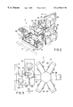
- FIGS. 1 to 16 show a substrate manufacturing apparatus according to an embodiment of the present invention, in which:
- FIG. 1 is a plan view schematically showing an outline of the manufacturing apparatus
- FIG. 2 is a perspective view showing a film forming device of the manufacturing apparatus
- FIG. 3 is a plan view of the film forming device
- FIG. 4 is a perspective view showing a cassette stage section and a transfer robot of the film forming device
- FIG. 5 is a sectional view of a cassette storing glass substrates
- FIG. 6 is a sectional view showing a glass substrate in the cassette and position sensors
- FIG. 7A is a sectional view schematically showing the positional relation between the glass substrate and the position sensors in a standby position
- FIG. 7B is a sectional view schematically showing the positional relation between the glass substrate and the position sensors in a detecting position
- FIG. 8 is an enlarged plan view of a hand portion of the transfer robot
- FIG. 9 is a block diagram showing a configuration of the transfer robot
- FIG. 10A is a plan view showing the positional relation between the glass substrate in the cassette and the hand in a reference position
- FIG. 10B is a plan view showing the positional relation between the glass substrate in the cassette and the hand in a position corrected for a shift or deviation of the substrate from the reference position;
- FIGS. 11A to 11 G are plan views individually showing processes of transportation of the glass substrate by the transfer robot
- FIGS. 12A to 12 C are plan views individually showing processes of inclination detecting operation for the glass substrate and hand correcting operation;
- FIG. 13 is a plan view showing a laser annealing device of the substrate manufacturing apparatus
- FIG. 14 is a perspective view schematically showing the inside of an annealing chamber of the laser annealing device
- FIG. 15 is a sectional view of the annealing chamber
- FIG. 16 is a perspective view showing a wet etching device of the substrate manufacturing apparatus
- FIG. 17 is a sectional view showing an example of an array substrate manufactured by means of the substrate manufacturing apparatus
- FIGS. 18A to 18 C are sectional views individually showing processes of manufacture of the array substrate by the substrate manufacturing apparatus
- FIGS. 19A to 19 E are sectional views individually showing further processes of manufacture of the array substrate by the substrate manufacturing apparatus
- FIG. 20 is a plan view showing a film forming device according to another embodiment of the invention.
- FIG. 21 is a perspective view showing a modification of the wet etching device
- FIG. 22 is a plan view showing a modification of the laser annealing device.
- FIG. 23 is a plan view schematically showing a substrate manufacturing apparatus according to still another embodiment of the invention.
- FIGS. 1 to 16 An embodiment of the present invention applied to a substrate manufacturing apparatus for manufacturing an array substrate of a liquid crystal display device will now be described in detail with reference to the accompanying drawings of FIGS. 1 to 16 .
- the substrate manufacturing apparatus is an apparatus for manufacturing an array substrate of a liquid crystal display panel that is used in a color liquid crystal display device of an active-matrix type, for example.
- This apparatus subjects a glass substrate (to-be-treated object) for forming the array substrate to various treatments.
- the substrate manufacturing apparatus comprises a transportation device (AGV) 7 for transporting the glass substrate along a predetermined transportation path, e.g., rectilinear transportation path A, and a plurality of treatment devices arranged along the path A.
- AAV transportation device
- the treatment devices include a film forming device 2 for forming a thin film of a desired material on the glass substrate, laser annealing device 3 for subjecting a film formed on the glass substrate to laser annealing, dry etching device 4 , ion doping device 5 , wet etching device 6 , etc.
- the general operation of the substrate manufacturing apparatus is controlled by means of a control device that is provided with a CPU (not shown) and the like.
- the film forming device 2 includes a cassette station 12 located near the transportation path A, treatment section 21 opposed to the station 12 , and spin-washing unit 16 deviated sideways from the line of arrangement of the station 12 and the section 21 .
- the device 2 further includes a transfer robot 15 , which is located between the cassette station 12 and the treatment section 21 .
- the robot 15 serves to transfer the glass substrate between the cassette station 12 , treatment section 21 , and washing unit 16 .
- the cassette station 12 includes two cassette stage sections 12 a that are arranged along the transportation path A. Each stage section 12 a removably carries thereon a cassette C, which stores a plurality of glass substrates 1 stacked in layers.
- the transportation device 7 is provided with a transfer vehicle 7 a that runs self-propelled along the transportation path A. The vehicle 7 a carries thereon and automatically delivers the cassettes C to a cassette station of any of the treatment devices.
- each glass substrate 1 is in the form of a rectangle that is 500 mm long, 400 mm wide, and 0.7 mm thick, for example.
- Each cassette C is a box that is composed of a top plate 103 , a bottom plate 104 , a plurality of side plates 105 , and a back plates (not shown).
- Formed in the front face of the cassette C is an opening 106 through which the glass substrates 1 are loaded into or unloaded from the cassette.
- a plurality of ledges 107 protrude from the inner surface of each side plate 105 .
- the ledges 107 are arranged vertically at predetermined intervals.
- Each glass substrate 1 is supported horizontally in the cassette C with its opposite side edge portions placed individually on the opposite ledges 107 . A large number of glass substrates 1 are stored vertically in layers in the cassette C.
- each side plate 105 in each stage is formed having a given clearance from its corresponding side edge of the glass substrate 1 so that the substrate 1 can be prevented from touching the inner surface 108 as it is loaded into or unloaded from the cassette C.
- a distance L 1 between the opposite inner surfaces is greater than a width L 2 of the substrate 1 (L 1 >L 2 ).
- each cassette stage section 12 a in the cassette station 12 is composed of a pair of support legs 14 that are set up on the top surface of the station 12 .
- the legs 14 extend parallel to each other in a Y-direction that is perpendicular to the transportation path A.
- Formed on the upper end face of each leg 14 moreover, is a positioning groove 14 a that extends in the Y-direction.
- the cassette C is positioned with respect to the cassette stage section 12 a in a manner such that two opposite side edge portions of its bottom plate 104 are fitted individually in the positioning grooves 14 a .
- the opening 106 of the cassette C opens in the Y-direction toward the treatment section 21 .
- Two cassettes C placed individually on the two cassette stage sections 12 a are situated in the extending direction of the transportation path A or an X-direction, and their respective central axes D extend parallel to the Y-direction.
- each cassette stage section 12 a is provided with a position detecting section 110 for detecting the position of each glass substrate 1 in the cassette C placed thereon.
- the detecting section 110 includes a pair of position sensors 112 for individually detecting the respective positions of a pair of side edges of the substrate 1 that extend in the Y-direction.
- a pair of support posts 114 are set up substantially vertically near their corresponding cassette stage sections 12 a .
- the posts 114 are arranged in the X-direction, facing each other with the stage sections 12 a between them.
- the position sensors 112 are supported individually by the support posts 114 so that they can move up and down in the vertical direction or Z-direction.
- each of the sensors 112 is movable in the X-direction between a retreated position in which it is situated outside the cassette C and a detecting position in which it is situated overlapping the side edge of any one of the glass substrates 1 .
- the position sensors 112 are located in positions such that a line that connects them passes substantially through a center h of the substrate 1 .
- the position sensors 112 in the retreated positions are moved in the Z-direction to a position such that they individually face the opposite side edges of any glass substrate, especially the glass substrate 1 that is to be taken out of the cassette C by means of the transfer robot 15 , which will be mentioned later.
- each position sensor 112 is moved in the X-direction from the retreated position toward the glass substrate 1 , and is stopped when it detects its corresponding side edge of the substrate 1 , as shown in FIG. 7 B. As this is done, the movement of each position sensor 112 is detected.
- the position of the glass substrate 1 is detected in accordance with the respective movements of the sensors 112 .
- the respective movements of the two position sensors 112 are equal, it is indicated that the glass substrate 1 is located with its center h in alignment with the central axis D of the cassette C. If the respective movements of the sensors 112 are different, their difference indicates that the glass substrate 1 is located with its central axis deviated in the X-direction from the central axis D of the cassette C. At the same time, the deviation can be detected. The deviation of the glass substrate 1 detected in this manner can be utilized as position information when the glass substrate is transported in the manner described later.
- the treatment section 21 of the film forming device 2 is located side by side with the cassette station 12 in the Y-direction.
- the treatment section 21 which is of a multi-chamber type, is provided with a load-locking chamber 22 that can be controlled for the atmospheric pressure or vacuum.
- the chamber 22 extends in the Y-direction, having one end thereof opposed to the cassette station 12 .
- a vacuum transfer chamber 24 having a substantially hexagonal plane shape is located on the other end side of the load-locking chamber 22 in a manner such that one side thereof is in contact with the chamber 22 .
- a heating chamber 26 for heating the glass substrate 1 and four film forming chambers 25 for forming a thin film on the substrate 1 by chemical vapor deposition are provided individually on the other five sides of the vacuum transfer chamber 24 .
- the chambers 26 and 25 function as separate treatment sections, and each of the film forming chambers is depressurized.
- the spin-washing unit 16 of the film forming device 2 serves to clean the glass substrate 1 taken out of the cassette C by spin-washing.
- the unit 16 is arranged adjacent to the cassette station 12 and the treatment section 21 , and is deviated from a space between itself and the station 12 in a second direction or X-direction perpendicular to a first direction or Y-direction passing through the station 12 and the section 21 are connected.
- the transfer robot 15 of the film forming device 2 is provided between the cassette station 12 and the load-locking chamber 22 of the treatment section 21 .
- the robot 15 takes out the glass substrate 1 from the cassette C and loads it into the spin-washing unit 16 . After the substrate 1 is washed, the robot 15 loads it into the treatment section 21 through the chamber 22 . When a film is formed on the glass substrate 1 in the section 21 , the robot 15 takes out the substrate and returns it to the cassette C.
- the transfer robot 15 which serves as a transportation mechanism, is provided with a hand 128 as a support member for supporting the glass substrate 1 , as shown in FIGS. 2 and 8.
- the hand 128 is designed so that it can move in two directions across a center point O within a horizontal plane, that is, in the X- and Y-directions, and ascend and descend in the vertical direction or Z-direction across the center point O. Further, the hand 128 is rockable around the Z-axis.
- the transfer robot 15 includes a base 120 provided between the cassette station 12 and the load-locking chamber 22 of the treatment section 21 and a driving section 123 movable along a guide groove 122 , which is formed in the base 120 and extends in the X-direction.
- the groove 122 extends in a direction across the center of the spin-washing unit 16 .
- the driving section 123 for use as drive means, includes a rotating shaft 125 , which can ascend and descend along the Z-axis and rotate in the ⁇ -direction around the Z-axis.
- the shaft 125 is in alignment with the center point O.
- the driving section 123 is located on the base 120 so that it can turn itself around the Z-axis.
- One end portion of a first arm 124 is connected to the rotating shaft 125 so that the arm 124 is rockable integrally with the shaft 125 .
- One end of a second arm 126 is connected to the other end of the first arm 124 for rotation around a rotating shaft 127 .
- the hand 128 for carrying the glass substrate 1 is connected to the other end of the second arm 126 for rotation around a rotating shaft 129 .
- the first and second arms 124 and 126 constitute a link. As the first arm 124 rocks, the second arm 126 rocks for a given angle.
- the hand 128 is formed of a thin plate that extends horizontally.
- the proximal end portion of the hand 128 is connected to the rotating shaft 129 , and the distal end portion thereof is bifurcated right and left.
- the hand 128 is mounted on the rotating shaft 129 in a manner such that its center line d is in alignment with a movement axis M that extends across the shaft 129 and the center point O.
- the hand 128 moves in the X-direction.
- the arms 124 and 126 ascend or descend together with the rotating shaft 125 , the hand 128 moves in the Z-direction.
- the hand 128 moves along the movement axis M with its center line d continually in alignment with the axis M.
- the driving section 123 rocks around the center point O, furthermore, the hand 128 rocks together with the first and second arms 124 and 126 around the center point O.
- the hand 128 is provided with first and second non-contact sensors 130 a and 130 b for detecting one side 1 a of the glass substrate 1 on the opening side of the cassette C in two positions.
- the sensors 130 a and 130 b are of an optical reflector type, using infrared rays that have an optical focusing point such that they can be detected without being transmitted through the transparent glass substrate 1 .
- the sensors 130 a and 130 b are arranged bisymmetrically with respect to the center line d (line that passes through the rotating shaft 29 and the center point O) of the hand 128 , that is, on a line perpendicular to the center line d, with their detecting surfaces upward.
- the sensors are arranged with a space x 1 of 200 mm between them.
- a substrate mounting reference line R is set at a distance y 1 of, for example, 100 mm from the first and second sensors 130 a and 130 b on the proximal side of the hand 128 . As the glass substrate 1 is transported, it is supported on the hand 128 with its one end la in alignment with the reference line R.
- the position sensors 112 and the first and second sensors 130 a and 130 b are connected to a control section 141 , which functions as control means and adjusting means. Further, the control section 141 is connected with a driver 142 for driving the driving section 123 of the transfer robot 15 .
- the control section 141 includes a main controller 144 for controlling the basic transporting operation of the robot 15 , an arithmetic element 146 for calculating the relative positions of the hand 128 and the glass substrate 1 in accordance with information on the output signals of the sensors 112 , 130 a and 130 b and the operating state of the robot 15 , and a correcting section 148 for outputting a correction signal for correcting the transporting operation of the robot 15 in accordance with the calculated position.
- the following is a description of the loading and unloading operations of the transfer robot 15 constructed in this manner. Let it be supposed that the cassettes C transported by the AGV 7 are placed individually on the cassette stage sections. 12 a , and that the glass substrates 1 are stored in layers in each cassette C. The hand 128 of the robot 15 is supposed to be located in its standby position.
- the center point O of the transfer robot 15 is situated on the X-axis and a reference axis RY that extends coaxially with the central axis D of one cassette C.
- the hand 128 is located in a position such that its center line d is in alignment with the reference axis RY, and the movement axis M of the hand 128 is also in alignment with the axis YR.
- the position of the substrate 1 or a deviation of the center h of the substrate from the central axis D of the cassette C is detected by means of the position sensors 112 of the position detecting section 110 in the cassette station 12 . If the center of the glass substrate 1 to be taken out is deviated from the central axis D by a distance a in the X-direction, the driving section 123 moves for the distance a in the X-direction, thereby correcting the deviation of the substrate 1 .
- the reference axis RY of the transfer robot 15 and the center line d and movement axis M of the hand 128 pass through the center h of the glass substrate 1 and extend parallel to the central axis D of the cassette C, as shown in FIG. 10 B.
- the transfer robot 15 moves the hand 128 in the Z-axis direction under the control of the control section 141 , as shown in FIG. 11A, and stops at a height such that the hand 128 is situated under the glass substrate 1 to be taken out of the cassette C and that the space between the undersurface of the substrate 1 and the first and second sensors 130 a and 130 b is equal to a given distance or 8 mm in this case.
- the hand 128 is moved along the reference axis RY into the cassette C, as shown in FIGS. 11B and 12A, and gets into the space between the glass substrate 1 to be taken out and the glass substrate 1 thereunder or the bottom plate 104 of the cassette C.
- the first and second sensors 130 a and 130 b cross the region under the one side 1 a of the substrate 1 , and individually detect the side 1 a and output detection signals.
- the control section 141 concludes that there is no glass substrate 1 in the cassette C and stops the transfer operation. If only one of the first and second sensors 130 a and 130 b outputs its detection signal, the control section 141 concludes that the glass substrate 1 is broken.
- the arithmetic element 146 of the control section 141 computes a Y-direction distance of movement y 2 of the hand 128 covered during the time interval between the departure from the standby position and the detection of the one side la of the glass substrate 1 by the first sensor 130 a and a Y-direction distance of movement y 3 covered before the detection of the one side la by the second sensor 130 b.
- the control section 141 Based on the distances of movement y 2 and y 3 , moreover, the control section 141 computes the inclination of the glass substrate 1 , that is, an inclination ⁇ 1 of the substrate with respect to the reference axis RY, and the RY-direction (reference-axis-direction) position of the substrate 1 as one-side-position information. Based on this result of computation, the control section 141 computes the moving direction of the hand 128 corresponding to the inclination of the glass substrate 1 and the necessary distance of movement of the hand 128 for the alignment of the one side 1 a of the substrate 1 with the substrate mounting reference line R of the hand 128 .
- control section 141 After the control section 141 then returns the hand 128 to the standby position, it actuates the transfer robot 15 so that the hand 128 is situated in a predetermined position relative to the glass substrate 1 . More specifically, as shown in FIGS. 11C and 12B, the control section 141 moves the driving section 123 to the right for a distance of movement x 2 along the X-axis so that a line connecting the first and second sensors 130 a and 130 b extends parallel to the one side 1 a of the glass substrate 1 . Further, the control section 141 causes the driving section 123 , along with the arms 124 and 126 , to rotate for ⁇ 1 in the counterclockwise direction around the center point O. By doing this, the movement axis M and center line d of the hand 128 match the inclination of the glass substrate 1 .
- the control section 141 computes a distance of movement y 4 of the hand 128 in the direction of the movement axis M.
- the substrate mounting reference line R of the hand 128 is set at the distance y 1 from the line that connects the first and second sensors 130 a and 130 b .
- the control section 141 corrects data on the movement axis M and rocked position of the hand 128 . Thereafter, the control section 141 controls the operation of the transfer robot 15 in accordance with the corrected data.
- the hand 128 moves to a predetermined mounting position corresponding to the takeout position for the glass substrate 1 , and is stopped at the mounting position. Thereupon, the center line d of the hand 128 is aligned with the center line of the glass substrate 1 , and the reference line R of the hand 128 with the one side la of the substrate 1 .
- the distances of movement y 2 and y 3 computed in accordance with the detection signals from the first and second sensors 130 a and 130 b are equal, that is, if the glass substrate 1 to be taken out is in its correct position such that its one side 1 a extends at right angles to the central axis d of the hand 128 , the angle of inclination of the substrate 1 is computed to be 0°, and the control section 141 moves the hand 128 along the reference axis RY to the predetermined mounting position without correcting its moving direction.
- the position of the hand 128 relative to the glass substrate 1 is corrected after the hand 128 is returned to the standby position.
- the hand 128 may be subjected to position correction without being returned to the standby position.
- the transfer robot 15 raises the hand 128 for a given distance in the Z-direction.
- the hand 128 supports the glass substrate 1 and pushes it up to a height position at a given distance (gap) from the ledges 107 of the cassette C.
- the transfer robot 15 moves the hand 128 along the movement axis M to a position over the driving section 123 , as shown in FIG. 11E, and takes out the glass substrate 1 on the hand 128 from the cassette C. Then, the robot 15 rotates the driving section 123 , along with the arms 124 and 126 and the hand 128 , for 90°+ ⁇ 1 in the clockwise direction around the center point O, thereby opposing the substrate 1 to the spin-washing unit 16 and aligning the center line of the substrate 1 with the X-axis, as shown in FIGS. 11F and 12C. At the same time, the hand 128 is moved in the Z-direction to be adjusted to a predetermined height position corresponding to the washing unit 16 .
- control section 141 moves the driving section 123 in a direction opposite to the correcting direction for a distance equal to an X-direction correction value a and x 2 for the takeout of the glass substrate 1 , thereby aligning the reference axis RY of the transfer robot 15 with the center line D of the cassette C, as shown in FIG. 12 C.
- the control section 141 moves the driving section 123 and the hand 128 for a given distance in the X-direction toward the spin-washing unit 16 .
- the transfer robot 15 moves the hand 128 along the movement axis M or in the X-direction to the washing unit 16 , thereby loading the glass substrate 1 on the hand 128 into a predetermined position in the unit 16 , as shown in FIG. 11 E.
- the robot 15 is returned to the predetermined standby position.
- the transfer robot 15 takes out the substrate 1 from the unit 16 under the control of the control section 141 , and moves it to a position opposite to the load-locking chamber 22 of the treatment section 21 . Thereafter, the robot 15 loads the substrate 1 into the chamber 22 in the Y-direction.
- the transfer robot 15 takes out the substrate 1 from the load-locking chamber 22 , and moves in the X-direction to a position opposite to any of the cassettes C, thereby transporting the substrate 1 . Thereafter, the robot 15 loads the substrate 1 onto specified ledges in the cassette C in the Y-direction.
- the transfer robot 15 transports the glass substrate 1 from the cassette C in the X-direction and loads it into the spin-washing unit 16 . After the substrate 1 is washed, the robot 15 transports it in the Y-direction and loads it into treatment section 21 . Further, the robot 15 transports the treated substrate 1 from the treatment section 21 in the Y-direction and returns it to the cassette C.
- the annealing device 3 includes a cassette station 32 , an excimer-laser annealing (ELA) chamber 37 as a treatment section, a spin-washing unit 36 , and a transfer robot 35 .
- the cassette station 32 is opposed to the transportation path A of the transportation device 7 .
- the annealing chamber 37 is opposed to the station 32 in the Y-direction perpendicular to the path A.
- the washing unit 36 is deviated from the line of arrangement of the station 32 and the chamber 37 in the X-direction along the transportation path A.
- the robot 35 which is located between the cassette station 32 and the annealing chamber 37 , serves to transfer the glass substrate between the station 32 , chamber 37 , and unit 36 .
- the cassette station 32 includes two cassette stage sections 32 a that are arranged along the transportation path A. Each stage section 32 a is constructed in the same manner as each cassette stage section 12 a of the film forming device 2 . Each stage section 32 a removably carries thereon a cassette C, which has the same construction as aforesaid and stores a plurality of glass substrates 1 stacked in layers.
- a washing chamber of the spin-washing unit 36 is opposed to the transfer robot 35 through an openable gate 36 a .
- the laser annealing chamber 37 is also opposed to the robot 35 through an openable gate 37 a .
- the gates 36 a and 37 a can separate atmospheres in the spin-washing unit 36 and the annealing chamber 37 from an atmosphere in a space for the cassette station 32 and the transfer robot 35 .
- the glass substrate 1 is taken out of the cassette C, transported in the X-direction, and loaded directly into the spin-washing unit 36 by the transfer robot 35 , as indicated by arrow A 1 in FIG. 13 .
- the substrate 1 is taken out of the washing unit 36 , transported in the X- and Y-directions, and loaded directly into the laser annealing chamber 37 .
- the substrate 1 subjected to laser annealing in the annealing chamber 37 is taken out of the chamber 37 , transported in the Y-direction, and loaded into the cassette C by the robot 35 .
- the laser annealing device 3 includes a laser generator 38 for applying an excimer laser to the annealing chamber 37 .
- the generator 38 is provided with an excimer laser source 38 a and an optical system including a beam homogenizer (not shown) for guiding a generated laser as a linear beam, optical mirrors 38 b and 38 c , and the like.
- a stage 37 b Arranged inside the annealing chamber 37 are a stage 37 b for substantially horizontally supporting the glass substrate 1 and an atmosphere separating cover 39 situated over the substrate 1 that is supported on the stage 37 b .
- the cover 39 is in the form of a cylinder having a flat elliptic cross section, and its upper end is airtightly fixed to the inner surface of a top wall 37 c of the annealing chamber 37 .
- a top opening of the cover 39 faces a laser window 33 , which is formed of a quartz glass or the like embedded in the top wall 37 c .
- a bottom opening of the cover 39 faces a laser irradiation region of the glass substrate 1 on the stage 37 b across a narrow gap G.
- the excimer laser generated from the laser generator 38 is reflected by the optical mirrors 38 b and 38 c of the optical system, projected on the inside of the atmosphere separating cover 39 through the laser window 33 , and applied to the glass substrate 1 through the cover 39 .
- the supply section 40 is a gas control system that supplies the gases to the inside of the cover 39 to control the atmosphere.
- the gas supply section 40 includes pipes 40 a and 40 b for supplying, for example, nitrogen (N 2 ) and oxygen (O 2 ), gas control sections 40 c , such as solenoid valves, for opening and closing the pipes 40 a and 40 b to regulate the flow rates of the gases, and a concentration sensor 41 for detecting the oxygen concentration of the atmosphere inside the atmosphere separating cover 39 .
- the supply section 40 adjusts the atmosphere inside the cover 39 or in the laser irradiation region of the surface of the glass substrate 1 to a given oxygen concentration.
- a nitrogen atmosphere may be used having the oxygen concentration at 0.1% to 13%, preferably at 1.0% to 7.0%.
- oxygen and nitrogen are supplied separately.
- oxygen and nitrogen may be mixed to a predetermined oxygen concentration before they are supplied. It is necessary only that the oxygen concentration of the atmosphere be kept at a given value at least in a region near the glass substrate surface inside the separating cover 39 .
- the dry etching device 4 is located in line with the film forming device 2 and the laser annealing device 3 along the transportation path A.
- the device 4 includes a cassette station 42 , a dry etching chamber 47 and a spin-washing unit 46 as treatment sections, and a transfer robot 45 .
- the cassette station 42 is opposed to the transportation path A.
- the chamber 47 and the unit 46 are opposed to the station 42 in the Y-direction perpendicular to the path A.
- the robot 45 which is located between the cassette station 42 on one side and the dry etching chamber 47 and the spin-washing unit 46 on the other side, serves to transfer the glass substrate between the station 42 , chamber 47 , and unit 46 .
- the cassette station 42 includes two cassette stage sections that are arranged along the transportation path A. Each stage section is constructed in the same manner as each cassette stage section 12 a of the film forming device 2 . Each stage section removably carries thereon a cassette C, which has the same construction as aforesaid and stores a plurality of glass substrates 1 stacked in layers.
- the glass substrate 1 is taken out of the cassette C, transported in the Y-direction, and loaded into the spin-washing unit 46 by the transfer robot 45 .
- the substrate 1 is taken out of the washing unit 46 , transported in the X- and Y-directions, and loaded directly into the dry etching chamber 47 .
- a film formed on the substrate 1 is subjected to dry etching.
- the etched substrate 1 is taken out of the chamber 47 , transported in the Y-direction, and loaded into the cassette C by the robot 45 .
- the ion doping device 5 is located in line with the dry etching device 4 along the transportation path A.
- the device 5 includes a cassette station 52 , an ion doping chamber 57 and a spin-washing unit 56 as treatment sections, and a transfer robot 55 .
- the cassette station 52 is opposed to the transportation path A.
- the chamber 57 and the unit 56 are opposed to the station 52 in the Y-direction perpendicular to the path A.
- the robot 55 which is located between the cassette station 52 on one side and the ion doping chamber 57 and the spin-washing unit 56 on the other side, serves to transfer the glass substrate between the station 52 , chamber 57 , and unit 56 .
- the cassette station 52 includes two cassette stage sections that are arranged along the transportation path A. Each stage section is constructed in the same manner as each cassette stage section 12 a of the film forming device 2 . Each stage section removably carries thereon a cassette C, which has the same construction as aforesaid and stores a plurality of glass substrates 1 stacked in layers.
- the glass substrate 1 is taken out of the cassette C, transported in the Y-direction, and loaded into the spin-washing unit 56 by the transfer robot 55 .
- the substrate 1 is taken out of the washing unit 56 , transported in the X- and Y-directions, and loaded directly into the ion doping chamber 57 .
- a film formed on the substrate 1 is doped with ions.
- the doped substrate 1 is taken out of the chamber 57 , transported in the Y-direction, and loaded into the cassette C by the robot 55 .
- the wet etching device 6 is located in line with the ion doping device 5 along the transportation path A.
- the device 6 includes a cassette station 62 , a standby stage 71 , a treatment section 72 , and a transfer robot 65 .
- the cassette station 62 is opposed to the transportation path A.
- the stage 71 is opposed to the station 62 in the Y-direction perpendicular to the path A.
- the section 72 is located side by side with the stage 71 in the Y-direction.
- the robot 65 which is located between the standby stage 71 and the cassette station . 62 , serves to transfer the glass substrate 1 between the station 62 and the stage 71 .
- the cassette station 62 includes three cassette stage sections 63 that are arranged along the transportation path A. Each stage section 63 is constructed in the same manner as each cassette stage section 12 a of the film forming device 2 . Each stage section 63 removably carries thereon a cassette C, which has the same construction as aforesaid and stores a plurality of glass substrates 1 stacked in layers. A control panel 66 is located beside the cassette station 62 .
- the standby stage 71 is composed of two tiers, upper and lower.
- the transfer robot 65 loads the glass substrate 1 taken out of the cassette C into the stage 71 in the Y-direction, takes out the treated substrate 1 from the stage 71 , and loads it into the cassette C in the Y-direction.
- the robot 65 is constructed substantially in the same manner as the transfer robot of the film forming device 2 .
- the treatment section 72 is provided with four square medical fluid treatment sections 73 as separate treatment sections.
- Each treatment section 73 includes a cup 74 having a diameter greater than the diagonal of the glass substrate 1 .
- a substrate chuck 75 is provided in the center of the cup 74 .
- the chuck 75 which can rotate and move up and down holding the substrate 1 , can adjust the substrate 1 to the same temperature as a medical fluid.
- Rotatable medical fluid nozzles 76 are arranged over the cups 74 , and a transfer robot 77 is located in the center of the four medical fluid treatment sections 73 .
- the four medical fluid treatment sections 73 are provided with a control system for controlling their temperatures and other factors as a whole or individually.
- the treatment sections 73 are capable of spin drying or air-blow drying.
- an array substrate B comprises a glass substrate 1 as an insulated substrate.
- Protective films 82 of SiN x and SiON are successively formed in layers on the substrate 1 .
- a channel region 84 , drain region 85 , and source region 86 of poly-silicon (p-Si) are formed on the film 83 .
- the regions 85 and 86 are situated individually on the opposite sides of the channel region 84 .
- a gate insulating film 87 of SiO 2 or TEOS is formed on the channel, drain, and source regions 84 , 85 and 86 , and a metallic gate electrode 88 of aluminum or aluminum alloy is formed on the insulating film 87 .
- An interlayer insulating film 89 of SiN x is formed covering the film 87 and the electrode 88 .
- the films 89 and 87 are formed having contact holes 90 and 91 , respectively.
- a drain electrode 92 and a source electrode 93 of aluminum or aluminum alloy are formed penetrating the holes 90 and 91 , respectively.
- the electrodes 92 and 93 constitute a thin-film transistor 94 .
- the array substrate B further comprises pixel electrodes, signal lines, scanning lines, etc., which are not shown.
- the glass substrate 1 stored in the cassette C is transported along the transportation path A to a position where it faces the cassette station 12 of the film forming device 2 . Thereafter, the cassette C is transferred to the cassette stage section 12 a of the station 12 .
- the glass substrate 1 After the glass substrate 1 is then taken out in the Y-direction from the cassette C by means of the transfer robot 15 , it is loaded into the spin-washing unit 16 that is situated in the X-direction perpendicular to the Y-direction. The substrate 1 is washed by means of the washing unit 16 . Subsequently, the washed glass substrate 1 is taken out in the X-direction from the unit 16 by means of the robot 15 , and is then loaded into the load-locking chamber 22 of the treatment section 21 in the Y-direction within 20 seconds, preferably 10 seconds.
- the load-locking chamber 22 When loaded with the glass substrate 1 , the load-locking chamber 22 is decompressed to a vacuum from the atmospheric pressure. Then, the substrate 1 is transferred from the chamber 22 to the heating chamber 26 through the vacuum transfer chamber 24 by means of the transfer robot (not shown), and is heated at a given temperature for a given time in the chamber 26 . Thereafter, the glass substrate 1 is transferred from the heating chamber 26 to the different film forming chambers 25 in succession through the vacuum transfer chamber 24 . Thereupon, SiN x and SiON films for the protective films 82 and 83 and an amorphous silicon (a-Si) film for the channel, drain, and source regions 84 , 85 and 86 are successively formed on the substrate 1 in the film forming chambers, as shown in FIG. 18 A.
- a-Si amorphous silicon
- the glass substrate 1 having the SiN x , SiON, and a-Si films thereon, is transported to the load-locking chamber 22 by means of the vacuum transfer chamber 24 . After the chamber 22 is restored from the vacuum to the atmospheric pressure, the substrate 1 is transported in the Y-direction to be returned to the cassette C by the transfer robot 15 .
- the cassette C is transferred to the transfer vehicle 7 a and transported along the transportation path A to a position where it faces the cassette station 32 of the laser annealing device 3 . Further, the cassette C is transferred to one of the cassette stage sections 32 a of the station 32 .
- each glass substrate 1 is taken out of the cassette C and loaded directly into the spin-washing unit 36 by the transfer robot 35 , as indicated by arrow A 1 in FIG. 13 .
- pretreatments such as removal of particles, removal of phosphorus, boron, and other impurities, are carried out.
- the transfer robot 35 takes out the glass substrate 1 from the spin-washing unit 36 , transports it in the X- and Y-directions, and loads it directly into the annealing chamber 37 through the open gate 37 a , as indicated by arrow A 2 in FIG. 13 .
- the time for the transportation from the washing unit 36 to the annealing chamber 37 is not longer than about 20 seconds, preferably about 10 seconds. Accordingly, the time for the transfer of the substrate 1 to the annealing chamber 37 immediately after the end of the pretreatments is constant and very short, so that the probability of impurities, such as phosphorus, boron, etc., or particles adhering again to the glass substrate is minimized. Since the glass substrate 1 is transferred between the unit 36 and the chamber 37 only once by the transfer robot 35 , moreover, the probability of particles adhering to the substrate 1 is low.
- the glass substrate 1 is mounted in a predetermined position on the stage 37 b , and the atmosphere separating cover 39 is situated over the substrate 1 with the narrow gap G between the two.
- the gas supply section 40 supplies the gases to the inside of the cover 39 in accordance with measurement data obtained by means of the oxygen concentration sensor 41 , thereby controlling the atmosphere near the laser irradiation region on the glass substrate 1 , e.g., oxygen concentration, to be a fixed value.
- the atmosphere of the annealing chamber 37 is not a vacuum atmosphere, but is at a pressure not lower than normal pressure, that is, at normal pressure or a given positive pressure.
- an excimer laser is generated from the laser generator 38 , guided as a linear beam by means of the optical system, transmitted through the laser window 33 and the atmosphere separating cover 39 , and applied to the glass substrate 1 .
- the glass substrate 1 is gradually moved by a predetermined distance so that the respective regions applied with the linear beams are partially overlapped with each other. More specifically, as shown in FIG. 18B, the a-Si layer formed on the substrate 1 is annealed by means of the excimer laser and crystallized into a poly-silicon (p-Si) film 95 for forming the channel, drain, and source regions 84 , 85 and 86 . Thereafter, the glass substrate 1 , having the crystallized p-Si film thereon, is returned to the cassette C by the transfer robot 35 , as indicated by arrow A 3 in FIG. 13 .
- the cassette C is transferred to the transfer vehicle 7 a and transported along the transportation path A to a photo-etching device (not shown).
- a photo-etching process a resist is formed on the channel, drain, and source regions 84 , 85 and 86 .
- each glass substrate 1 is taken out of the cassette C and loaded directly into the spin-washing unit 36 by the transfer robot 45 .
- the substrate 1 washed in the unit 36 , is then loaded directly into the dry etching chamber 47 by the robot 45 , a resist 96 and the p-Si film 95 are dry-etched in the form of an island, as shown in FIG. 18 C.
- the glass substrate 1 is returned to the cassette C by the robot 45 .
- the cassette C is transferred to the transfer vehicle 7 a and transported along the transportation path A to a position where it faces the cassette station of the next film forming device (not shown). Thereafter, the cassette C is placed on one of the cassette stage sections of this station.
- This film forming device is constructed in the same manner as the film forming device 2 .
- each glass substrate 1 from the cassette C is loaded into a spin-washing unit by a transfer robot. After it is washed, the substrate 1 is transferred directly from the washing unit to a load-locking chamber. After the substrate 1 is then heated in a heating chamber, it is transferred from the heating chamber to different film forming chambers in succession through a vacuum transfer chamber. Thereupon, an SiO 2 film for the insulating film 87 and a film of metal (MoW) for the gate electrode 88 are successively formed on the island-shaped p-Si film 95 , as shown in FIG. 19 A.
- MoW metal
- the glass substrate 1 having the SiO 2 film and the metal film thereon, is transported to the load-locking chamber through the vacuum transfer chamber. After the atmosphere is restored from the vacuum to the atmospheric pressure, the substrate 1 is returned to the cassette C by the transfer robot.
- the cassette C is transferred to the transfer vehicle 7 a and transported along the transportation path A to the photo-etching device (not shown).
- the photo-etching device By a photo-etching process, an island-shaped resist 97 is formed on the gate insulating film 87 and the gate electrode 88 , as shown in FIG. 19 A.
- the cassette C is transported by means of the truck 7 a to a position where it faces the cassette station of another dry etching device (not shown) that has the same construction as the dry etching device 2 . Further, the cassette C is transferred to one of the cassette stage sections of this station.
- each glass substrate 1 is taken out of the cassette C and loaded directly into a spin-washing unit by a transfer robot. After the substrate 1 , washed in the washing unit, is then loaded directly into a dry etching chamber by the robot, the gate electrode 88 is dry-etched into the form of an island, as shown in FIG. 19 B. Thereafter, the glass substrate 1 is returned to the cassette C by the transfer robot.
- the cassette C is transferred to the transfer vehicle 7 a and transported along the transportation path A to a position where it faces the cassette station 32 of the laser annealing device 3 . Further, the cassette C is transferred to one of the cassette stage sections of the cassette station 52 of the ion doping device 5 .
- each glass substrate 1 is taken out of the cassette C and loaded into the spin-washing unit 56 by the transfer robot 55 .
- the washed substrate I is loaded directly into the ion doping chamber 57 by the robot 55 .
- the p-Si film 95 is doped with ions with the gate electrode 88 used as a mask, as shown in FIG. 19 C.
- the channel region 84 is not ion-doped due to self-alignment of the gate electrode 88 , and only the drain and source regions 85 and 86 are doped with ions.
- the p-Si film may be formed having an LDD (lightly doped drain) structure by using a resist or metal film as a mask.
- LDD lightly doped drain
- the glass substrate 1 having its drain and source regions 85 and 86 doped with ions, is returned to the cassette C by the transfer robot 55 .
- the cassette C is transferred to the transfer vehicle 7 a and transported along the transportation path A to a film forming device (not shown), and the interlayer insulating film 89 is formed on the gate insulating film 87 and the gate electrode 88 . Further, the cassette C is transferred to the truck 7 a and transported along the path A to the photo-etching device (not shown). By a photo-etching process, a resist is formed covering those portions of the interlayer insulating film 89 which are expected to form the contact holes 90 and 91 .
- the cassette C is transferred to the transfer vehicle 7 a and transported along the transportation path A to a position where it faces the cassette station 62 of the wet etching device 6 . Further, the cassette C is transferred to one of the cassette stage sections 63 of the cassette station 62 .
- the glass substrates 1 from the cassette C are load alternately onto the two tiers of the standby stage 71 by the transfer robot 65 and heated in the stage 71 . Thereafter, the substrates 1 are successively transported by the transfer robot 77 to the two medical fluid treatment sections 73 that are supplied with a medical fluid for wet etching.
- the substrate chucks 75 holding the substrates 1 in a raised position are lowered so that the substrates 1 are situated individually in the cups 74 . Further, the substrates 1 are rotated by means of the chucks 75 as the medical fluid for wet etching is supplied through the nozzles 76 . Thereupon, the contact holes 90 and 91 are bored through the interlayer insulating film 89 and the gate insulating film 87 , as shown in FIG. 19 D.
- the substrate chucks 75 are raised to lift the glass substrates 1 , having the contact holes 90 and 91 therein, above the cups 74 . Then, the substrates 1 are successively transferred by the transfer robot 77 from the medical fluid treatment sections 73 that are supplied with the medical fluid for wet etching to the other treatment sections 73 that are supplied with a medical fluid for resist separation. Then, the substrates 1 are held by means of the substrate chucks 76 to be situated in the cups 4 , individually. Further, the substrates 1 are rotated by means of the chucks 75 as the medical fluid for resist separation is supplied thereto through the nozzles 76 , whereupon the resist is separated. The medical fluids can be replaced with new ones without lowering the operating efficiency of the device if they are changed when the treatment sections 73 concerned are not loaded with any substrates 1 .
- the glass substrates 1 cleared of the resist, are transported to the standby stage 71 by the transfer robot 77 and further loaded into the cassette C by the transfer robot 65 .
- the cassette C is transported along the transportation path A by means of the transfer vehicle 7 a of the transportation device 7 to a position where it faces the cassette station of the next film forming device, and is placed on one of the cassette stage sections of this station.
- This film forming device is constructed in the same manner as the aforementioned film forming device.
- each glass substrate 1 is taken out of the cassette C and loaded into the spin-washing unit 16 by the transfer robot 15 .
- the washed substrate 1 from the unit 16 is loaded directly into the load-locking chamber 22 within 20 seconds, preferably 10 seconds.
- the substrate 1 is transferred from the chamber 22 to the heating chamber 26 through the vacuum transfer chamber 24 and heated in the chamber 26 .
- the glass substrate 1 is transferred from the heating chamber 26 to the different film forming chambers 25 in succession through the transfer chamber 24 .
- a metal film for the drain and source electrodes 92 and 93 is formed on the interlayer insulating film 89 of the substrate 1 .
- the glass substrate 1 having the metal film thereon, is transported to the load-locking chamber 22 through the vacuum transfer chamber 24 , and is further returned to the cassette C by the transfer robot 15 .
- the cassette C is carried out along the transportation path A by the transportation device 7 , whereupon it advances to the next stage (not shown).
- the resulting structure is etched. By doing this, the drain and source electrodes 92 and 93 are formed, whereupon the array substrate B is completed, as shown in FIG. 19 E.
- the film forming device 2 , laser annealing device 3 , dry etching device 4 , and ion doping device 5 have their respective spin-washing units 16 , 36 , 46 and 56 .
- the cassette C need not be transported to any other independent washing device, so that the washed substrates can be loaded directly into the respective treatment sections of the devices.
- desired treatments can be carried out in a short time after the substrates are washed, and the washed substrates can be loaded into the treatment sections without any substantial contamination. In consequence, the yield of array substrate production is improved, and the lead time can be shortened.
- the transportation distance of the cassette C can be also shortened, the so-called Q-time can be managed with ease, and the whole manufacturing apparatus can be reduced in size.
- the spin-washing unit 16 is located in a dead space in the X-direction or the transportation direction of the transportation device 7 , compared to the treatment section 21 that is located in the Y-direction perpendicular to the transportation direction of the device 7 . Accordingly, a plurality of treatment sections can be arranged with higher efficiency, and the whole manufacturing apparatus can be reduced in size.
- the substrates are loaded individually into the four medical fluid treatment sections 73 by means of the transfer robot 77 that is movable over the range covering the treatment sections 73 . Accordingly, the installation area can be reduced, and the substrates can be transferred easily and securely between the standby stage 71 and the medical fluid treatment sections.
- the annealing chamber 37 of the laser annealing device is opposed directly to the transfer robot 15 so that the washed substrates can be loaded directly into the chamber 37 . Therefore, the component units of the laser annealing device and the transportation mechanism parts between the component units can be reduced in number.
- the construction of the device can be simplified so that sources of particles can be reduced to ensure annealing in a stable atmosphere. In consequence, the quality of the substrates can be improved.
- the annealing chamber 37 is designed so that laser annealing can be carried out in an atmosphere at a pressure not lower than normal pressure, that is, at normal pressure or a given positive pressure, not in a vacuum atmosphere. Accordingly, there is no need of a vacuum pump or the like, so that the construction can be simplified, and therefore, the manufacturing costs can be reduced.
- the spin-washing unit 36 is connected directly to the cassette station 32 . Therefore, the substrates can be transported to the annealing chamber 37 in a short time after carrying out pretreatments for annealing by means of the washing unit 36 . Accordingly, laser annealing can be effected in a manner such that particles are removed, and that non-crystalline silicon is prevented from natural oxidation or impurities, such as boron, phosphorus, etc., are removed and prevented from adhering to the substrates. Thus, the state of the thin film is stabilized, so that the transistor characteristics and other properties of the substrates can be improved.
- the atmosphere separating cover 39 that surrounds the laser irradiation region of each substrate is located in the annealing chamber 37 in which the laser is applied to the substrate, and the gases are supplied to the inside of the cover 39 by means of the gas supply section 40 .
- the necessary atmosphere portion for annealing, near the laser irradiation position in the chamber 37 can be controlled with ease. Accordingly, no impurities can get into the annealing chamber 37 despite the atmosphere at normal pressure or the given positive pressure, and the film state can be stabilized without using any expensive vacuum pump.
- the construction of the laser annealing device can be simplified to lower the manufacturing costs, and the gas consumption can be made less than in the case where the annealing chamber is filled up with gases. In consequence, operating costs of the apparatus can be reduced.
- the gas supply section 40 is provided with the oxygen concentration sensor 41 for detecting the atmosphere inside the atmosphere separating cover 39 and the gas control sections 40 c for controlling the gases supplied to the inside of the cover 39 . Therefore, annealing can be effected in a desired atmosphere, so that the quality of the substrates can be improved.
- the a-Si thin film can be converted into p-Si with a larger crystal grain size, for example. Further, the quality of the substrates can be improved by enhancing the mobility of the transistor characteristics or the like.
- the atmosphere separating cover 39 is opposed across the predetermined gap G to the stage 37 b that supports each substrate in the annealing chamber 37 . Owing to laminar flows of the gases that pass through the gap G, the atmosphere can enjoy a fixed oxygen concentration, so that annealing can be effected in a desired atmosphere. Thus, the quality of the substrates can be improved with use of a simple construction.
- the to-be-treated object for use as a substrate of a liquid crystal display panel, is annealed by means of an excimer laser.
- the a-Si film or non-crystalline silicon film that forms the channel, drain, and source regions 84 , 85 and 86 can be suitably crystallized into a p-Si film or polycrystalline silicon film.
- substrates of a desired quality can be obtained by loading the annealing chamber 37 with a nitrogen atmosphere.
- the oxygen concentration of the atmosphere in the chamber 37 is adjustable to 0.1% to 13%, preferably 1.0% to 7.0%.
- the a-Si thin film can be converted into p-Si with a larger crystal grain size, and the quality of the substrates can be improved by enhancing the mobility of the transistor characteristics or the like.
- the film forming device 2 is supposed to include the one load-locking chamber 22 , four film forming chambers 25 , and one heating chamber 26 .
- these chambers may be combined in any suitable numbers to improve the operating efficiency of the apparatus and shorten the treatment time.
- a film forming device 2 includes a cassette station 12 , which have three cassette stage sections 12 a arranged along a transportation path A, and two spin-washing units 16 a and 16 b located individually on the opposite sides of the station 12 in the X-direction.
- a treatment section 21 is provided with a pair of load-locking chambers 22 that are opposed to the station 12 in the Y-direction.
- the chambers 22 are arranged in the X-direction.
- the treatment section 21 includes one heating chamber 26 and four film forming chambers 25 .
- a transfer robot 15 is located between the two spin-washing units 16 a and 16 b and also between the cassette station 12 and the load-locking chambers 22 .
- Each spin-washing unit, heating chamber 26 , and each film forming chamber 25 are constructed in the same manner as their counterparts according to the foregoing embodiment.
- the individual parts of the transfer robot 15 which is of a double-hand type having two hands, resemble those of the transfer robot of the first embodiment in construction and operation.
- glass substrates stored in cassettes C are transported alternatively to the two spin-washing units 16 a and 16 b by the transfer robot 15 , as indicated by arrows in FIG. 20 . After they are washed, the substrates are loaded directly into their corresponding load-locking chambers 22 . The substrates are loaded into or unloaded from the washing units 16 a and 16 b in the X-direction. On the other hand, the glass substrates are loaded into or unloaded from each cassette C and each load-locking chamber 22 in the Y-direction that is perpendicular to the X-direction.
- Each glass substrate loaded into one of the load-locking chambers 22 is placed on a rotatable stage (not shown) in the chamber 22 , and is turned by the stage so that its center line passes through the center of a vacuum transfer chamber 24 . Subsequently, the glass substrate is transferred from the chamber 22 to the heating chamber 26 by a transfer robot 24 a in the transfer chamber 24 and heat-treated. Thereafter, the substrate is transferred from the chamber 26 to any of the film forming chambers 25 , whereupon a desired thin film is formed on the substrate. After the film formation, the glass substrate is transferred from the film forming chamber 25 to the load-locking chamber 22 by the robot 24 a . After the substrate is reoriented in the chamber 22 so that its center line extends parallel to the Y-direction, it is taken out of the chamber 22 and returned to the cassette C by the transfer robot 15 .
- the film forming device 2 includes the four film forming chambers 25 and the heating chamber 26 , and a wet etching chamber 6 includes four medical fluid treatment sections 73 .
- each treatment device may be formed by freely changing each of the chambers or treatment sections into a film forming chamber, heating chamber, laser annealing chamber, ion doping chamber, or medical fluid treatment section. By doing this, the course of treatment can be shorted to reduce the treatment time, and the operating efficiency of the apparatus can be further improved.
- the wet etching device 6 is provided with the four medical fluid treatment sections 73 . As shown in FIG. 21, however, the same effect can be obtained with use of a device that is provided with only two medical fluid treatment sections 73 without including any standby stage.
- the medical fluid treatment sections 73 of the wet etching device 6 may use one and the same specific medical fluid or different fluids, such as a sensitizing agent, resist solution, developing agent, etching solution, release agent, pure water, ionic water, etc.
- a sensitizing agent such as resist solution, developing agent, etching solution, release agent, pure water, ionic water, etc.
- at least one of functions for various processes including a medical fluid process, developing process, etching process, resist-coating process, purifying process, and drying process, may be given to each of a plurality of medical fluid treatment sections 73 .
- one treatment device can be enabled continuously or alternatively to execute the resist-coating process, developing process, etching process, releasing process, and washing process.
- the one annealing chamber 37 is opposed to the one cassette station 32 .
- a plurality of annealing chambers 37 may be opposed to the one cassette station 32 .
- the spin-washing unit 36 may be located side by side with the annealing chamber 37 in the X-direction that is parallel to the transportation path A, as shown in FIG. 22 .
- the washing unit 36 for washing the substrates may be designed for post-treatments for annealing as well as for the pretreatments.
- nitrogen gas or the like are used as the atmosphere of the annealing chamber 37 or the atmosphere inside the atmosphere separating cover 39 according to the foregoing embodiment, any other gases, e.g., argon or other inert gases, may be used for the purpose.
- a substrate manufacturing apparatus comprises a plurality of treatment chambers 150 that are arranged at predetermined intervals.
- a stocker 152 which can carry a plurality of cassettes thereon, is provided on one end side of each treatment chamber.
- a main transportation path B of a main transportation device 154 and a transfer vehicle 154 a are arranged on the ceiling of a plant in which the substrate manufacturing apparatus is installed.
- the truck 154 a is movable along the path B.
- the main transportation path B is in the form of an elongate track, part of which extends over the stockers 152 .
- the truck 154 a which can bear a plurality of cassettes thereon, is designed to move to a position over any one of the stockers 152 and deliver to or receive the cassettes from the stocker.
- the device 156 includes a transportation path D in the form of an elongate track, extending at right angles to the main transportation path B, and a transfer vehicle 156 a that runs self-propelled along the path D.
- the truck 154 a which can bear a plurality of cassettes thereon, is designed to transfer the cassettes between the stockers 152 and between treatment devices (mentioned later) in the treatment chambers 150 on either side.
- a plurality of treatment devices are arranged in each treatment device 150 .
- identical treatment devices for the same treatment are arranged side by side along the respective side edges of each two adjacent treatment chambers 150 on either side of each auxiliary transportation device 156 that face the device 156 .
- CVD film forming devices
- PEP photo-etching devices
- ELA excimer laser annealing device
- Each film forming device 2 and each excimer laser annealing device 3 are constructed in the same manner as their counterparts according to the foregoing embodiments.
- each treatment chamber 150 can be improved relatively easily by collectively arranging a plurality of treatment devices in each treatment chamber so that they are isolated from the outside.
Abstract
Description
Claims (17)
Priority Applications (1)
| Application Number | Priority Date | Filing Date | Title |
|---|---|---|---|
| US09/867,525 US6588232B1 (en) | 1998-01-13 | 2001-05-31 | Treatment device, laser annealing device, manufacturing apparatus, and manufacturing apparatus for flat display device |
Applications Claiming Priority (4)
| Application Number | Priority Date | Filing Date | Title |
|---|---|---|---|
| JP517698 | 1998-01-13 | ||
| JP10-005176 | 1998-01-13 | ||
| JP17751698 | 1998-06-24 | ||
| JP10-177516 | 1998-06-24 |
Related Child Applications (1)
| Application Number | Title | Priority Date | Filing Date |
|---|---|---|---|
| US09/867,525 Division US6588232B1 (en) | 1998-01-13 | 2001-05-31 | Treatment device, laser annealing device, manufacturing apparatus, and manufacturing apparatus for flat display device |
Publications (1)
| Publication Number | Publication Date |
|---|---|
| US6270619B1 true US6270619B1 (en) | 2001-08-07 |
Family
ID=26339085
Family Applications (2)
| Application Number | Title | Priority Date | Filing Date |
|---|---|---|---|
| US09/229,581 Expired - Lifetime US6270619B1 (en) | 1998-01-13 | 1999-01-13 | Treatment device, laser annealing device, manufacturing apparatus, and manufacturing apparatus for flat display device |
| US09/867,525 Expired - Lifetime US6588232B1 (en) | 1998-01-13 | 2001-05-31 | Treatment device, laser annealing device, manufacturing apparatus, and manufacturing apparatus for flat display device |
Family Applications After (1)
| Application Number | Title | Priority Date | Filing Date |
|---|---|---|---|
| US09/867,525 Expired - Lifetime US6588232B1 (en) | 1998-01-13 | 2001-05-31 | Treatment device, laser annealing device, manufacturing apparatus, and manufacturing apparatus for flat display device |
Country Status (4)
| Country | Link |
|---|---|
| US (2) | US6270619B1 (en) |
| JP (1) | JP2000150411A (en) |
| KR (3) | KR100324915B1 (en) |
| TW (1) | TW444275B (en) |
Cited By (36)
| Publication number | Priority date | Publication date | Assignee | Title |
|---|---|---|---|---|
| US6461437B1 (en) * | 2000-01-26 | 2002-10-08 | Mitsubishi Denki Kabushiki Kaisha | Apparatus used for fabricating liquid crystal device and method of fabricating the same |
| US20030019578A1 (en) * | 2001-07-27 | 2003-01-30 | Dainippon Screen Mfg. Co., Ltd. | Substrate processing apparatus equipping with high-pressure processing unit |
| US6540869B2 (en) * | 2000-06-02 | 2003-04-01 | Tokyo Electron Limited | Semiconductor processing system |
| US20030066752A1 (en) * | 2000-07-08 | 2003-04-10 | Ritzdorf Thomas L. | Apparatus and method for electrochemical processing of a microelectronic workpiece, capable of modifying processes based on metrology |
| US20030082914A1 (en) * | 2000-03-13 | 2003-05-01 | Yutaka Koma | Semiconductor wafer processing apparatus |
| US6580053B1 (en) * | 2000-08-31 | 2003-06-17 | Sharp Laboratories Of America, Inc. | Apparatus to control the amount of oxygen incorporated into polycrystalline silicon film during excimer laser processing of silicon films |
| US6594560B2 (en) * | 2000-07-26 | 2003-07-15 | Samsung Electronics Co., Ltd. | Automated-guided vehicle system and method for controlling the same |
| US20040064641A1 (en) * | 2001-07-13 | 2004-04-01 | Hitachi, Ltd. | Storage device with I/O counter for partial data reallocation |
| WO2004030048A1 (en) * | 2002-09-27 | 2004-04-08 | Asm America, Inc. | A system for the improved handling of wafers within a process tool |
| US20050061676A1 (en) * | 2001-03-12 | 2005-03-24 | Wilson Gregory J. | System for electrochemically processing a workpiece |
| US20050107971A1 (en) * | 2000-07-08 | 2005-05-19 | Ritzdorf Thomas L. | Apparatus and method for processing a microelectronic workpiece using metrology |
| US20050115492A1 (en) * | 2003-11-28 | 2005-06-02 | Chia-Cheng Liu | Method and apparatus of the chemical metal organic vapor epitaxy for the multi-chamber epitaxy layer deposition |
| US20060183070A1 (en) * | 2003-09-25 | 2006-08-17 | Hitachi Kosusai Electric Inc. | Substrate processing device and method of producing substrates |
| US7102763B2 (en) * | 2000-07-08 | 2006-09-05 | Semitool, Inc. | Methods and apparatus for processing microelectronic workpieces using metrology |
| US20070017607A1 (en) * | 2003-05-17 | 2007-01-25 | Mtu Aero Engines Gmbh | Method for heating components |
| US20070231477A1 (en) * | 2006-03-17 | 2007-10-04 | Lg.Philips Lcd Co., Ltd. | System and method for manufacturing liquid crystal display panel, and liquid crystal display panel using the same |
| US20070246664A1 (en) * | 2001-09-10 | 2007-10-25 | Shunpei Yamazaki | Laser apparatus, laser irradiation method, semiconductor manufacturing method, semiconductor device, and electronic equipment |
| CN100401338C (en) * | 2004-02-25 | 2008-07-09 | 爱德牌工程有限公司 | Apparatus for manufacturing flat-panel display |
| US20090248192A1 (en) * | 2006-06-15 | 2009-10-01 | Tokyo Electron Limited | Substrate processing system and substrate conveyance method |
| US20090283499A1 (en) * | 2003-10-20 | 2009-11-19 | Novellus Systems, Inc. | Fabrication of semiconductor interconnect structure |
| US20100015805A1 (en) * | 2003-10-20 | 2010-01-21 | Novellus Systems, Inc. | Wet Etching Methods for Copper Removal and Planarization in Semiconductor Processing |
| US7811925B1 (en) * | 2005-10-13 | 2010-10-12 | Novellus Systems, Inc. | Capping before barrier-removal IC fabrication method |
| US20100297786A1 (en) * | 2006-03-22 | 2010-11-25 | Nitto Koki Kabushiki Kaisha | Method for Manufacturing Compound Semiconductor and Apparatus for Manufacturing the Same |
| US20110056913A1 (en) * | 2009-09-02 | 2011-03-10 | Mayer Steven T | Reduced isotropic etchant material consumption and waste generation |
| US20120003064A1 (en) * | 2009-03-18 | 2012-01-05 | Oc Oerlikon Balzers Ag | Vacuum treatment apparatus |
| US20120252160A1 (en) * | 2011-04-01 | 2012-10-04 | Semiconductor Energy Laboratory Co., Ltd. | Method for manufacturing semiconductor device |
| US8470191B2 (en) | 2003-10-20 | 2013-06-25 | Novellus Systems, Inc. | Topography reduction and control by selective accelerator removal |
| US8530359B2 (en) | 2003-10-20 | 2013-09-10 | Novellus Systems, Inc. | Modulated metal removal using localized wet etching |
| WO2013143677A1 (en) * | 2012-03-30 | 2013-10-03 | Innolas Semiconductor GmbH | Handling unit for wafers and method for picking up a wafer |
| US20160133502A1 (en) * | 2014-11-07 | 2016-05-12 | Jung-min Won | Wafer transfer robot, method of controlling the same, and method of manufacturing a semiconductor device using the same |
| US9660092B2 (en) | 2011-08-31 | 2017-05-23 | Semiconductor Energy Laboratory Co., Ltd. | Oxide semiconductor thin film transistor including oxygen release layer |
| US20180122678A1 (en) * | 2016-10-31 | 2018-05-03 | Semiconductor Manufacturing International (Shanghai) Corporation | Wafer alignment method and apparatus for overlay measurement |
| US20190135556A1 (en) * | 2017-11-09 | 2019-05-09 | Nidec Sankyo Corporation | Work transfer system and control method thereof |
| CN110923659A (en) * | 2018-09-20 | 2020-03-27 | 东京毅力科创株式会社 | Film forming method and substrate processing system |
| KR20200033752A (en) * | 2018-09-20 | 2020-03-30 | 도쿄엘렉트론가부시키가이샤 | Film forming method and substrate processing system |
| CN114269666A (en) * | 2019-08-22 | 2022-04-01 | 川崎重工业株式会社 | Substrate transfer robot, substrate transfer system, and substrate transfer method |
Families Citing this family (8)
| Publication number | Priority date | Publication date | Assignee | Title |
|---|---|---|---|---|
| TW588403B (en) * | 2001-06-25 | 2004-05-21 | Tokyo Electron Ltd | Substrate treating device and substrate treating method |
| US7363777B2 (en) * | 2004-03-05 | 2008-04-29 | Corning Incorporated | Closed cassette and method for heat treating glass sheets |
| US8022104B2 (en) * | 2005-02-24 | 2011-09-20 | Yissum Research Development Company Of The Hebrew University Of Jerusalem | Formulations of ladostigil tartrate |
| US8042359B2 (en) * | 2006-05-18 | 2011-10-25 | Corning Incorporated | Methods and apparatus for heat treating glass sheets |
| CN102834899B (en) * | 2010-04-12 | 2015-08-05 | 株式会社日本制钢所 | Laser machining device |
| US8893527B1 (en) * | 2011-07-21 | 2014-11-25 | WD Media, LLC | Single surface annealing of glass disks |
| CN104064489B (en) * | 2013-03-22 | 2016-10-05 | 上海和辉光电有限公司 | Automation dispatching method, device and ELA board prepare control system |
| JP7185671B2 (en) * | 2020-09-23 | 2022-12-07 | 株式会社Screenホールディングス | SUBSTRATE PROCESSING APPARATUS AND SUBSTRATE PROCESSING METHOD |
Citations (10)
| Publication number | Priority date | Publication date | Assignee | Title |
|---|---|---|---|---|
| JPH05217918A (en) | 1992-02-07 | 1993-08-27 | Tokyo Electron Ltd | Film forming apparatus |
| JPH05283348A (en) | 1992-03-30 | 1993-10-29 | Kokusai Electric Co Ltd | Longitudinal cvd device |
| JPH0778759A (en) | 1992-12-04 | 1995-03-20 | Semiconductor Energy Lab Co Ltd | Method and device of manufacturing semiconductor material |
| JPH08274143A (en) | 1995-02-02 | 1996-10-18 | Tokyo Electron Ltd | Device and method for carrying substrate |
| JPH09139356A (en) | 1995-11-16 | 1997-05-27 | Japan Steel Works Ltd:The | Laser annealing treatment apparatus |
| JPH09246198A (en) | 1996-03-01 | 1997-09-19 | Matsushita Electric Ind Co Ltd | Manufacture of high mobility polycrystal silicon thin film |
| JPH09260275A (en) | 1996-03-25 | 1997-10-03 | Tokyo Electron Ltd | Treatment method and treatment equipment |
| US5700127A (en) * | 1995-06-27 | 1997-12-23 | Tokyo Electron Limited | Substrate processing method and substrate processing apparatus |
| JPH1031316A (en) | 1996-07-17 | 1998-02-03 | Dainippon Screen Mfg Co Ltd | Treating device for substrate |
| US5923966A (en) * | 1994-07-28 | 1999-07-13 | Semiconductor Energy Laboratory Co., Ltd. | Laser processing method |
Family Cites Families (7)
| Publication number | Priority date | Publication date | Assignee | Title |
|---|---|---|---|---|
| JPS567436A (en) | 1979-06-29 | 1981-01-26 | Sony Corp | High pressure treating device |
| JPS6428809A (en) | 1987-07-23 | 1989-01-31 | Fujitsu Ltd | Laser annealing device |
| JPH02177423A (en) | 1988-12-28 | 1990-07-10 | Sharp Corp | Manufacture of single crystal thin film and device therefor |
| JPH07109573A (en) * | 1993-10-12 | 1995-04-25 | Semiconductor Energy Lab Co Ltd | Glass substrate and heat treatment |
| JP3735394B2 (en) | 1995-06-16 | 2006-01-18 | ソニー株式会社 | Method for manufacturing thin film semiconductor device |
| FR2737806B1 (en) * | 1995-08-11 | 1997-09-12 | Soc D Production Et De Rech Ap | LASER SURFACE TREATMENT DEVICE AND METHOD |
| JPH118205A (en) | 1997-04-25 | 1999-01-12 | Sharp Corp | Manufacture of semiconductor device and laser beam irradiation device |
-
1999
- 1999-01-12 TW TW088100413A patent/TW444275B/en not_active IP Right Cessation
- 1999-01-13 KR KR1019990004307A patent/KR100324915B1/en not_active IP Right Cessation
- 1999-01-13 US US09/229,581 patent/US6270619B1/en not_active Expired - Lifetime
- 1999-11-29 JP JP11338515A patent/JP2000150411A/en active Pending
-
2001
- 2001-05-24 KR KR10-2001-0028664A patent/KR100380789B1/en not_active IP Right Cessation
- 2001-05-24 KR KR1020010028665A patent/KR100348127B1/en not_active IP Right Cessation
- 2001-05-31 US US09/867,525 patent/US6588232B1/en not_active Expired - Lifetime
Patent Citations (10)
| Publication number | Priority date | Publication date | Assignee | Title |
|---|---|---|---|---|
| JPH05217918A (en) | 1992-02-07 | 1993-08-27 | Tokyo Electron Ltd | Film forming apparatus |
| JPH05283348A (en) | 1992-03-30 | 1993-10-29 | Kokusai Electric Co Ltd | Longitudinal cvd device |
| JPH0778759A (en) | 1992-12-04 | 1995-03-20 | Semiconductor Energy Lab Co Ltd | Method and device of manufacturing semiconductor material |
| US5923966A (en) * | 1994-07-28 | 1999-07-13 | Semiconductor Energy Laboratory Co., Ltd. | Laser processing method |
| JPH08274143A (en) | 1995-02-02 | 1996-10-18 | Tokyo Electron Ltd | Device and method for carrying substrate |
| US5700127A (en) * | 1995-06-27 | 1997-12-23 | Tokyo Electron Limited | Substrate processing method and substrate processing apparatus |
| JPH09139356A (en) | 1995-11-16 | 1997-05-27 | Japan Steel Works Ltd:The | Laser annealing treatment apparatus |
| JPH09246198A (en) | 1996-03-01 | 1997-09-19 | Matsushita Electric Ind Co Ltd | Manufacture of high mobility polycrystal silicon thin film |
| JPH09260275A (en) | 1996-03-25 | 1997-10-03 | Tokyo Electron Ltd | Treatment method and treatment equipment |
| JPH1031316A (en) | 1996-07-17 | 1998-02-03 | Dainippon Screen Mfg Co Ltd | Treating device for substrate |
Cited By (63)
| Publication number | Priority date | Publication date | Assignee | Title |
|---|---|---|---|---|
| US6461437B1 (en) * | 2000-01-26 | 2002-10-08 | Mitsubishi Denki Kabushiki Kaisha | Apparatus used for fabricating liquid crystal device and method of fabricating the same |
| US20030082914A1 (en) * | 2000-03-13 | 2003-05-01 | Yutaka Koma | Semiconductor wafer processing apparatus |
| US6540869B2 (en) * | 2000-06-02 | 2003-04-01 | Tokyo Electron Limited | Semiconductor processing system |
| US7161689B2 (en) | 2000-07-08 | 2007-01-09 | Semitool, Inc. | Apparatus and method for processing a microelectronic workpiece using metrology |
| US7102763B2 (en) * | 2000-07-08 | 2006-09-05 | Semitool, Inc. | Methods and apparatus for processing microelectronic workpieces using metrology |
| US20030066752A1 (en) * | 2000-07-08 | 2003-04-10 | Ritzdorf Thomas L. | Apparatus and method for electrochemical processing of a microelectronic workpiece, capable of modifying processes based on metrology |
| US20050107971A1 (en) * | 2000-07-08 | 2005-05-19 | Ritzdorf Thomas L. | Apparatus and method for processing a microelectronic workpiece using metrology |
| US6594560B2 (en) * | 2000-07-26 | 2003-07-15 | Samsung Electronics Co., Ltd. | Automated-guided vehicle system and method for controlling the same |
| US6580053B1 (en) * | 2000-08-31 | 2003-06-17 | Sharp Laboratories Of America, Inc. | Apparatus to control the amount of oxygen incorporated into polycrystalline silicon film during excimer laser processing of silicon films |
| US20050061676A1 (en) * | 2001-03-12 | 2005-03-24 | Wilson Gregory J. | System for electrochemically processing a workpiece |
| US20040064641A1 (en) * | 2001-07-13 | 2004-04-01 | Hitachi, Ltd. | Storage device with I/O counter for partial data reallocation |
| US6841031B2 (en) * | 2001-07-27 | 2005-01-11 | Dainippon Screen Mfg. Co., Ltd. | Substrate processing apparatus equipping with high-pressure processing unit |
| US20030019578A1 (en) * | 2001-07-27 | 2003-01-30 | Dainippon Screen Mfg. Co., Ltd. | Substrate processing apparatus equipping with high-pressure processing unit |
| US8044372B2 (en) * | 2001-09-10 | 2011-10-25 | Semiconductor Energy Laboratory Co., Ltd. | Laser apparatus, laser irradiation method, semiconductor manufacturing method, semiconductor device, and electronic equipment |
| US20070246664A1 (en) * | 2001-09-10 | 2007-10-25 | Shunpei Yamazaki | Laser apparatus, laser irradiation method, semiconductor manufacturing method, semiconductor device, and electronic equipment |
| WO2004030048A1 (en) * | 2002-09-27 | 2004-04-08 | Asm America, Inc. | A system for the improved handling of wafers within a process tool |
| US20070017607A1 (en) * | 2003-05-17 | 2007-01-25 | Mtu Aero Engines Gmbh | Method for heating components |
| US7975376B2 (en) | 2003-09-25 | 2011-07-12 | Hitachi Kokusai Electric Inc. | Method of manufacturing a semiconductor device |
| US20100170436A1 (en) * | 2003-09-25 | 2010-07-08 | Hitachi Kokusai Electric Inc. | Substrate treatment equipment and manufacturing method of substrate |
| US8424485B2 (en) | 2003-09-25 | 2013-04-23 | Hitachi Kokusai Electric Inc. | Substrate treatment equipment and manufacturing method of substrate |
| US20080193274A1 (en) * | 2003-09-25 | 2008-08-14 | Hitachi Kokusai Electric Inc. | Substrate treatment equipment and manufacturing method of substrate |
| US8245389B2 (en) | 2003-09-25 | 2012-08-21 | Hitachi Kokusai Electric Inc. | Method of manufacturing a semiconductor device |
| US20060183070A1 (en) * | 2003-09-25 | 2006-08-17 | Hitachi Kosusai Electric Inc. | Substrate processing device and method of producing substrates |
| US8470191B2 (en) | 2003-10-20 | 2013-06-25 | Novellus Systems, Inc. | Topography reduction and control by selective accelerator removal |
| US8372757B2 (en) | 2003-10-20 | 2013-02-12 | Novellus Systems, Inc. | Wet etching methods for copper removal and planarization in semiconductor processing |
| US20100015805A1 (en) * | 2003-10-20 | 2010-01-21 | Novellus Systems, Inc. | Wet Etching Methods for Copper Removal and Planarization in Semiconductor Processing |
| US9074286B2 (en) | 2003-10-20 | 2015-07-07 | Novellus Systems, Inc. | Wet etching methods for copper removal and planarization in semiconductor processing |
| US8530359B2 (en) | 2003-10-20 | 2013-09-10 | Novellus Systems, Inc. | Modulated metal removal using localized wet etching |
| US7972970B2 (en) | 2003-10-20 | 2011-07-05 | Novellus Systems, Inc. | Fabrication of semiconductor interconnect structure |
| US20090283499A1 (en) * | 2003-10-20 | 2009-11-19 | Novellus Systems, Inc. | Fabrication of semiconductor interconnect structure |
| US8481432B2 (en) | 2003-10-20 | 2013-07-09 | Novellus Systems, Inc. | Fabrication of semiconductor interconnect structure |
| US20050115492A1 (en) * | 2003-11-28 | 2005-06-02 | Chia-Cheng Liu | Method and apparatus of the chemical metal organic vapor epitaxy for the multi-chamber epitaxy layer deposition |
| CN100401338C (en) * | 2004-02-25 | 2008-07-09 | 爱德牌工程有限公司 | Apparatus for manufacturing flat-panel display |
| US9447505B2 (en) | 2005-10-05 | 2016-09-20 | Novellus Systems, Inc. | Wet etching methods for copper removal and planarization in semiconductor processing |
| US8043958B1 (en) | 2005-10-13 | 2011-10-25 | Novellus Systems, Inc. | Capping before barrier-removal IC fabrication method |
| US7811925B1 (en) * | 2005-10-13 | 2010-10-12 | Novellus Systems, Inc. | Capping before barrier-removal IC fabrication method |
| US8415261B1 (en) | 2005-10-13 | 2013-04-09 | Novellus Systems, Inc. | Capping before barrier-removal IC fabrication method |
| US7663731B2 (en) | 2006-03-17 | 2010-02-16 | Lg Display Co., Ltd. | System and method for manufacturing liquid crystal display panel, and liquid crystal display panel using the same |
| US20070231477A1 (en) * | 2006-03-17 | 2007-10-04 | Lg.Philips Lcd Co., Ltd. | System and method for manufacturing liquid crystal display panel, and liquid crystal display panel using the same |
| DE102006055621B4 (en) * | 2006-03-17 | 2018-02-15 | Lg Display Co., Ltd. | System for manufacturing a liquid crystal display panel |
| US20100297786A1 (en) * | 2006-03-22 | 2010-11-25 | Nitto Koki Kabushiki Kaisha | Method for Manufacturing Compound Semiconductor and Apparatus for Manufacturing the Same |
| US8046095B2 (en) | 2006-06-15 | 2011-10-25 | Tokyo Electron Limited | Substrate processing system and substrate transfer method |
| US20090248192A1 (en) * | 2006-06-15 | 2009-10-01 | Tokyo Electron Limited | Substrate processing system and substrate conveyance method |
| US8870513B2 (en) * | 2009-03-18 | 2014-10-28 | Oerlikon Advanced Technologies Ag | Vacuum treatment apparatus |
| US20120003064A1 (en) * | 2009-03-18 | 2012-01-05 | Oc Oerlikon Balzers Ag | Vacuum treatment apparatus |
| US9074287B2 (en) | 2009-09-02 | 2015-07-07 | Novellus Systems, Inc. | Reduced isotropic etchant material consumption and waste generation |
| US8597461B2 (en) | 2009-09-02 | 2013-12-03 | Novellus Systems, Inc. | Reduced isotropic etchant material consumption and waste generation |
| US20110056913A1 (en) * | 2009-09-02 | 2011-03-10 | Mayer Steven T | Reduced isotropic etchant material consumption and waste generation |
| US8541266B2 (en) * | 2011-04-01 | 2013-09-24 | Semiconductor Energy Laboratory Co., Ltd. | Method for manufacturing semiconductor device |
| US20120252160A1 (en) * | 2011-04-01 | 2012-10-04 | Semiconductor Energy Laboratory Co., Ltd. | Method for manufacturing semiconductor device |
| US9660092B2 (en) | 2011-08-31 | 2017-05-23 | Semiconductor Energy Laboratory Co., Ltd. | Oxide semiconductor thin film transistor including oxygen release layer |
| WO2013143677A1 (en) * | 2012-03-30 | 2013-10-03 | Innolas Semiconductor GmbH | Handling unit for wafers and method for picking up a wafer |
| US20160133502A1 (en) * | 2014-11-07 | 2016-05-12 | Jung-min Won | Wafer transfer robot, method of controlling the same, and method of manufacturing a semiconductor device using the same |
| US20180122678A1 (en) * | 2016-10-31 | 2018-05-03 | Semiconductor Manufacturing International (Shanghai) Corporation | Wafer alignment method and apparatus for overlay measurement |
| EP3316039A3 (en) * | 2016-10-31 | 2018-07-18 | Semiconductor Manufacturing International Corporation (Shanghai) | Wafer alignment method and apparatus for overlay measurement |
| US10553470B2 (en) * | 2016-10-31 | 2020-02-04 | Semiconductor Manufacturing International (Shanghai) Corporation | Wafer alignment method and apparatus for overlay measurement |
| US20190135556A1 (en) * | 2017-11-09 | 2019-05-09 | Nidec Sankyo Corporation | Work transfer system and control method thereof |
| US10875726B2 (en) * | 2017-11-09 | 2020-12-29 | Nidec Sankyo Corporation | Work transfer system and control method thereof |
| CN110923659A (en) * | 2018-09-20 | 2020-03-27 | 东京毅力科创株式会社 | Film forming method and substrate processing system |
| KR20200033752A (en) * | 2018-09-20 | 2020-03-30 | 도쿄엘렉트론가부시키가이샤 | Film forming method and substrate processing system |
| US11171004B2 (en) * | 2018-09-20 | 2021-11-09 | Tokyo Electron Limited | Film forming method and substrate processing system |
| CN114269666A (en) * | 2019-08-22 | 2022-04-01 | 川崎重工业株式会社 | Substrate transfer robot, substrate transfer system, and substrate transfer method |
| CN114269666B (en) * | 2019-08-22 | 2024-02-06 | 川崎重工业株式会社 | Substrate transfer robot, substrate transfer system, and substrate transfer method |
Also Published As
| Publication number | Publication date |
|---|---|
| KR20010070928A (en) | 2001-07-27 |
| JP2000150411A (en) | 2000-05-30 |
| KR20010070929A (en) | 2001-07-27 |
| KR19990068240A (en) | 1999-08-25 |
| KR100348127B1 (en) | 2002-08-09 |
| KR100324915B1 (en) | 2002-02-28 |
| TW444275B (en) | 2001-07-01 |
| KR100380789B1 (en) | 2003-04-18 |
| US6588232B1 (en) | 2003-07-08 |
Similar Documents
| Publication | Publication Date | Title |
|---|---|---|
| US6270619B1 (en) | Treatment device, laser annealing device, manufacturing apparatus, and manufacturing apparatus for flat display device | |
| US5413958A (en) | Method for manufacturing a liquid crystal display substrate | |
| US7064089B2 (en) | Plasma treatment apparatus and method for plasma treatment | |
| US6861614B1 (en) | S system for the formation of a silicon thin film and a semiconductor-insulating film interface | |
| JP2965038B1 (en) | Vacuum processing equipment | |
| US6486437B2 (en) | Apparatus for transforming semiconducting thin layer | |
| KR100276376B1 (en) | Semiconductor manufacturing apparatus and thin film semiconductor device manufacturing method | |
| JP2002280321A (en) | Laser annealing device | |
| JPH08172050A (en) | Irradiator for laser beam and irradiating method of laser beam | |
| US20220359204A1 (en) | System, Semiconductor Device and Method | |
| JP3927634B2 (en) | Laser annealing method and thin film transistor manufacturing method | |
| JP3154983B2 (en) | Processing apparatus and substrate manufacturing apparatus for flat panel display | |
| JP3400396B2 (en) | Laser annealing apparatus and laser annealing method | |
| JP2001110742A (en) | Laser annealing method | |
| JP2001156154A (en) | Processing method, manufacturing method using the same, substrate manufacturing method and manufacturing apparatus | |
| JP4001647B2 (en) | Method for manufacturing crystalline semiconductor film | |
| JP3196132B2 (en) | Method for manufacturing liquid crystal display substrate, method for evaluating semiconductor crystal, method for manufacturing semiconductor crystal thin film, and apparatus for manufacturing semiconductor crystal thin film | |
| JP2001085701A (en) | Element having multilayer structure, its manufacturing device and its manufacturing method | |
| JP2001135706A (en) | Processing method | |
| JP3204188B2 (en) | Method for forming silicon thin film and apparatus for forming silicon thin film | |
| CN112236843A (en) | Laser annealing method, laser annealing apparatus, and method for manufacturing active matrix substrate | |
| US20220336238A1 (en) | Heating/cooling device and heating/cooling method | |
| JP2008028405A (en) | Semiconductor thin-film reforming apparatus | |
| JP2000114346A (en) | Transfer method of electronic components and its equipment | |
| JPH09148246A (en) | Method for forming polycrystal silicon and formation device |
Legal Events
| Date | Code | Title | Description |
|---|---|---|---|
| STCF | Information on status: patent grant |
Free format text: PATENTED CASE |
|
| FEPP | Fee payment procedure |
Free format text: PAYOR NUMBER ASSIGNED (ORIGINAL EVENT CODE: ASPN); ENTITY STATUS OF PATENT OWNER: LARGE ENTITY |
|
| FPAY | Fee payment |
Year of fee payment: 4 |
|
| FPAY | Fee payment |
Year of fee payment: 8 |
|
| FEPP | Fee payment procedure |
Free format text: PAYOR NUMBER ASSIGNED (ORIGINAL EVENT CODE: ASPN); ENTITY STATUS OF PATENT OWNER: LARGE ENTITY Free format text: PAYER NUMBER DE-ASSIGNED (ORIGINAL EVENT CODE: RMPN); ENTITY STATUS OF PATENT OWNER: LARGE ENTITY |
|
| AS | Assignment |
Owner name: KABUSHIKI KAISHA TOSHIBA,JAPAN Free format text: ASSIGNMENT OF ASSIGNORS INTEREST;ASSIGNORS:SUZUKI, NAOKI;HIRATA, NORIYUKI;SHIMIZU, MASATOSHI;AND OTHERS;REEL/FRAME:024573/0645 Effective date: 19990310 |
|
| AS | Assignment |
Owner name: TOSHIBA MOBILE DISPLAY CO., LTD.,JAPAN Free format text: ASSIGNMENT OF ASSIGNORS INTEREST;ASSIGNOR:KABUSHIKI KAISHA TOSHIBA;REEL/FRAME:024599/0063 Effective date: 20100625 Owner name: AFPD PTE., LTD.,SINGAPORE Free format text: ASSIGNMENT OF ASSIGNORS INTEREST;ASSIGNOR:TOSHIBA MOBILE DISPLAY CO., LTD.;REEL/FRAME:024599/0067 Effective date: 20100628 |
|
| AS | Assignment |
Owner name: AU OPTRONICS CORPORATION, TAIWAN Free format text: ASSIGNMENT OF ASSIGNORS INTEREST;ASSIGNOR:AFPD PTE., LTD;REEL/FRAME:024776/0183 Effective date: 20100727 |
|
| FPAY | Fee payment |
Year of fee payment: 12 |