US6281078B1 - Manufacturing process to eliminate ONO fence material in high density NAND-type flash memory devices - Google Patents
Manufacturing process to eliminate ONO fence material in high density NAND-type flash memory devices Download PDFInfo
- Publication number
- US6281078B1 US6281078B1 US08/993,344 US99334497A US6281078B1 US 6281078 B1 US6281078 B1 US 6281078B1 US 99334497 A US99334497 A US 99334497A US 6281078 B1 US6281078 B1 US 6281078B1
- Authority
- US
- United States
- Prior art keywords
- layer
- conductive layer
- over
- polysilicon
- portions
- Prior art date
- Legal status (The legal status is an assumption and is not a legal conclusion. Google has not performed a legal analysis and makes no representation as to the accuracy of the status listed.)
- Expired - Lifetime
Links
- 239000000463 material Substances 0.000 title claims abstract description 15
- 238000004519 manufacturing process Methods 0.000 title description 4
- 229910021420 polycrystalline silicon Inorganic materials 0.000 claims abstract description 28
- 229920005591 polysilicon Polymers 0.000 claims abstract description 28
- WQJQOUPTWCFRMM-UHFFFAOYSA-N tungsten disilicide Chemical compound [Si]#[W]#[Si] WQJQOUPTWCFRMM-UHFFFAOYSA-N 0.000 claims abstract description 18
- 229910021342 tungsten silicide Inorganic materials 0.000 claims abstract description 12
- KRHYYFGTRYWZRS-UHFFFAOYSA-N Fluorane Chemical compound F KRHYYFGTRYWZRS-UHFFFAOYSA-N 0.000 claims abstract description 7
- 229910000040 hydrogen fluoride Inorganic materials 0.000 claims abstract description 4
- 238000000034 method Methods 0.000 claims description 52
- 229910021417 amorphous silicon Inorganic materials 0.000 claims description 12
- 239000000758 substrate Substances 0.000 claims description 12
- 125000006850 spacer group Chemical group 0.000 claims description 11
- XUIMIQQOPSSXEZ-UHFFFAOYSA-N Silicon Chemical compound [Si] XUIMIQQOPSSXEZ-UHFFFAOYSA-N 0.000 claims description 9
- 229910052710 silicon Inorganic materials 0.000 claims description 9
- 239000010703 silicon Substances 0.000 claims description 9
- 239000000203 mixture Substances 0.000 claims description 8
- 238000000151 deposition Methods 0.000 claims description 7
- 229920002120 photoresistant polymer Polymers 0.000 claims description 5
- 238000010438 heat treatment Methods 0.000 claims description 2
- 230000001590 oxidative effect Effects 0.000 claims description 2
- 239000004065 semiconductor Substances 0.000 claims 10
- 230000000873 masking effect Effects 0.000 claims 2
- 238000004140 cleaning Methods 0.000 claims 1
- 239000007788 liquid Substances 0.000 claims 1
- 238000000059 patterning Methods 0.000 claims 1
- 230000007257 malfunction Effects 0.000 abstract description 2
- 229910052814 silicon oxide Inorganic materials 0.000 abstract 1
- KPACBFJTZSMBKD-OAQYLSRUSA-N 2-[2-[(4-carbamimidoylphenyl)carbamoyl]-6-methoxypyridin-3-yl]-5-[[(2s)-1-hydroxy-3,3-dimethylbutan-2-yl]carbamoyl]benzoic acid Chemical compound C=1C=C(C(N)=N)C=CC=1NC(=O)C1=NC(OC)=CC=C1C1=CC=C(C(=O)N[C@H](CO)C(C)(C)C)C=C1C(O)=O KPACBFJTZSMBKD-OAQYLSRUSA-N 0.000 description 21
- BLRPTPMANUNPDV-UHFFFAOYSA-N Silane Chemical compound [SiH4] BLRPTPMANUNPDV-UHFFFAOYSA-N 0.000 description 10
- 239000007789 gas Substances 0.000 description 10
- 230000008569 process Effects 0.000 description 10
- XYFCBTPGUUZFHI-UHFFFAOYSA-N Phosphine Chemical compound P XYFCBTPGUUZFHI-UHFFFAOYSA-N 0.000 description 8
- 238000005530 etching Methods 0.000 description 8
- 229910000065 phosphene Inorganic materials 0.000 description 8
- MHAJPDPJQMAIIY-UHFFFAOYSA-N Hydrogen peroxide Chemical compound OO MHAJPDPJQMAIIY-UHFFFAOYSA-N 0.000 description 6
- 229910000077 silane Inorganic materials 0.000 description 6
- XPDWGBQVDMORPB-UHFFFAOYSA-N Fluoroform Chemical compound FC(F)F XPDWGBQVDMORPB-UHFFFAOYSA-N 0.000 description 5
- 206010034962 Photopsia Diseases 0.000 description 5
- 238000007667 floating Methods 0.000 description 5
- 230000008021 deposition Effects 0.000 description 4
- 238000004518 low pressure chemical vapour deposition Methods 0.000 description 4
- 230000008901 benefit Effects 0.000 description 3
- 238000012986 modification Methods 0.000 description 3
- 230000004048 modification Effects 0.000 description 3
- 150000004767 nitrides Chemical class 0.000 description 3
- 230000003647 oxidation Effects 0.000 description 3
- 238000007254 oxidation reaction Methods 0.000 description 3
- QGZKDVFQNNGYKY-UHFFFAOYSA-N Ammonia Chemical compound N QGZKDVFQNNGYKY-UHFFFAOYSA-N 0.000 description 2
- XKRFYHLGVUSROY-UHFFFAOYSA-N Argon Chemical compound [Ar] XKRFYHLGVUSROY-UHFFFAOYSA-N 0.000 description 2
- 241000293849 Cordylanthus Species 0.000 description 2
- VEXZGXHMUGYJMC-UHFFFAOYSA-N Hydrochloric acid Chemical compound Cl VEXZGXHMUGYJMC-UHFFFAOYSA-N 0.000 description 2
- 230000015572 biosynthetic process Effects 0.000 description 2
- 230000008878 coupling Effects 0.000 description 2
- 238000010168 coupling process Methods 0.000 description 2
- 238000005859 coupling reaction Methods 0.000 description 2
- 229910000041 hydrogen chloride Inorganic materials 0.000 description 2
- IXCSERBJSXMMFS-UHFFFAOYSA-N hydrogen chloride Substances Cl.Cl IXCSERBJSXMMFS-UHFFFAOYSA-N 0.000 description 2
- 239000007943 implant Substances 0.000 description 2
- 238000011065 in-situ storage Methods 0.000 description 2
- XLYOFNOQVPJJNP-UHFFFAOYSA-N water Substances O XLYOFNOQVPJJNP-UHFFFAOYSA-N 0.000 description 2
- VHUUQVKOLVNVRT-UHFFFAOYSA-N Ammonium hydroxide Chemical compound [NH4+].[OH-] VHUUQVKOLVNVRT-UHFFFAOYSA-N 0.000 description 1
- KZBUYRJDOAKODT-UHFFFAOYSA-N Chlorine Chemical compound ClCl KZBUYRJDOAKODT-UHFFFAOYSA-N 0.000 description 1
- ZAMOUSCENKQFHK-UHFFFAOYSA-N Chlorine atom Chemical compound [Cl] ZAMOUSCENKQFHK-UHFFFAOYSA-N 0.000 description 1
- CPELXLSAUQHCOX-UHFFFAOYSA-N Hydrogen bromide Chemical compound Br CPELXLSAUQHCOX-UHFFFAOYSA-N 0.000 description 1
- 229910021529 ammonia Inorganic materials 0.000 description 1
- 229910052786 argon Inorganic materials 0.000 description 1
- 230000015556 catabolic process Effects 0.000 description 1
- 239000000460 chlorine Substances 0.000 description 1
- 229910052801 chlorine Inorganic materials 0.000 description 1
- 239000011248 coating agent Substances 0.000 description 1
- 238000000576 coating method Methods 0.000 description 1
- 238000007598 dipping method Methods 0.000 description 1
- 230000006870 function Effects 0.000 description 1
- 239000001307 helium Substances 0.000 description 1
- 229910052734 helium Inorganic materials 0.000 description 1
- SWQJXJOGLNCZEY-UHFFFAOYSA-N helium atom Chemical compound [He] SWQJXJOGLNCZEY-UHFFFAOYSA-N 0.000 description 1
- 239000011159 matrix material Substances 0.000 description 1
- 238000001465 metallisation Methods 0.000 description 1
- 238000009877 rendering Methods 0.000 description 1
- 238000007789 sealing Methods 0.000 description 1
Images


Classifications
-
- H—ELECTRICITY
- H01—ELECTRIC ELEMENTS
- H01L—SEMICONDUCTOR DEVICES NOT COVERED BY CLASS H10
- H01L29/00—Semiconductor devices adapted for rectifying, amplifying, oscillating or switching, or capacitors or resistors with at least one potential-jump barrier or surface barrier, e.g. PN junction depletion layer or carrier concentration layer; Details of semiconductor bodies or of electrodes thereof ; Multistep manufacturing processes therefor
- H01L29/40—Electrodes ; Multistep manufacturing processes therefor
- H01L29/401—Multistep manufacturing processes
- H01L29/4011—Multistep manufacturing processes for data storage electrodes
- H01L29/40114—Multistep manufacturing processes for data storage electrodes the electrodes comprising a conductor-insulator-conductor-insulator-semiconductor structure
-
- H—ELECTRICITY
- H10—SEMICONDUCTOR DEVICES; ELECTRIC SOLID-STATE DEVICES NOT OTHERWISE PROVIDED FOR
- H10B—ELECTRONIC MEMORY DEVICES
- H10B41/00—Electrically erasable-and-programmable ROM [EEPROM] devices comprising floating gates
- H10B41/30—Electrically erasable-and-programmable ROM [EEPROM] devices comprising floating gates characterised by the memory core region
-
- H—ELECTRICITY
- H10—SEMICONDUCTOR DEVICES; ELECTRIC SOLID-STATE DEVICES NOT OTHERWISE PROVIDED FOR
- H10B—ELECTRONIC MEMORY DEVICES
- H10B69/00—Erasable-and-programmable ROM [EPROM] devices not provided for in groups H10B41/00 - H10B63/00, e.g. ultraviolet erasable-and-programmable ROM [UVEPROM] devices
Definitions
- This invention relates to memory cells and methods for manufacture thereof. Specifically, the invention relates to a method for manufacturing memory cells free of ONO fence material.
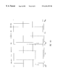
- FIG. 1 shows a cross-sectional view of a portion of a core cell in a NAND-type flash memory device.
- Fabrication of a NAND-type flash memory device involves depositing a lower polysilicon (“poly I”) layer 2 over tunnel oxide layer 8 and etching it so as to provide the structure shown over active region 10 of FIG. 2 .
- poly I polysilicon
- FIG. 2 depicts, for example, an edge of the structure of poly I layer 2 not overlapping a flat region of a core field oxide region 12 . Consequently, a recess 14 forms in poly I layer 2 over a sloping portion of core field oxide region 12 that may appear along the entire edge of poly I layer 2 .
- recess 14 can be caused by a horizontal etching of poly I layer 2 .
- Recess 14 harbors ONO 4 and poly II layer 6 materials from subsequent ONO 4 and poly II layer 6 depositions.
- poly I layer 2 After depositing and etching poly I layer 2 ; as shown in FIG. 1, a triple layer consisting of an oxide-nitride-oxide (“ONO”) stack, shown as ONO 4 , and polysilicon (“poly II”) layer 6 are provided above the poly I layer 2 structure. A tungsten silicide layer 93 and a silicon oxy-nitride (SiON) layer 94 are formed next.
- ONO oxide-nitride-oxide
- poly II polysilicon
- FIG. 3 corresponds to a top view of the structure of FIG. 1 .
- core field oxide regions 40 a and 40 b correspond to portions of core field oxide regions 12 of FIG. 1;
- active region 42 corresponds to a portion of active region 10 of FIG. 1; and
- poly I layer 66 corresponds to a portion of poly I layer 2 of FIG. 1 .
- the poly II layer 6 forms in the recess 14 , it may not be removed from the recess 14 in shaded region 100 of FIG. 3 .
- the poly II layer 6 in the recess 14 also may shield ONO 4 from removal from the recess 14 present in shaded region 100 of FIG. 3 .
- Remaining ONO 4 (“ONO fence” 16 ) further shields poly I layer 2 from removal from the shaded region 100 of FIG. 3 .
- edges of the etched poly I layer 2 may overlap with top, flat portions of core field oxide regions 12 and consequently recesses 14 may be absent from the poly I layer 2 as shown in FIG. 4 .
- ONO fences 16 may remain.
- FIG. 5A shows a top view of the structure 60 of FIG. 4 after the removal steps described earlier.
- ONO fences 16 appear, for example, at positions 48 a , 48 b , 48 c , and 48 d of FIG. 5 A.
- ONO fences 16 shield some poly I layer 2 material from removal during the removal steps. Remaining poly I materials present, for example, at positions 48 a , 48 b , 48 c , and 48 d of FIG. 5A (“polystringers” 18 ) electrically short NAND-type memory cells.
- FIG. 5B depicts a cross section of the structure 62 of FIG. 5A showing ONO fence 16 and polystringers 18 .
- Structure 70 of FIG. 5B corresponds, for example, to a cross section along line X 2 —X 2 of structure 62 of FIG. 5 A.
- core field oxide regions 12 correspond to portions of core field oxide regions 40 a and 40 b of FIG. 5A
- active region 10 corresponds to a portion of active region 42 of FIG. 5 A.
- Poly I layer 46 of FIG. 5A corresponds to a portion of poly I layer 2 of FIG. 4 .
- FIG. 6A depicts a matrix of NAND-type flash memory core cells 22 with polystringers occurring, for example, at positions 20 . Consequently, as shown in FIGS. 6A and 6B, following etching, an “ONO fence” 16 , portions of poly II layer 6 , and portions of poly I layer 2 may remain at positions 20 .
- FIG. 6B corresponds, for example, to a cross section along line X—X of the structure of FIG. 6 A.
- FIG. 6B depicts a position 20 that may include portions of poly II layer 6 and portions of poly I layer 2 that constitute polystringers 18 that. electrically short NAND-type flash memory core cells 22 , thereby rendering the flash memory core cells inoperable.
- the present invention removes ONO fence that shield polystringers from removal. Polystringers that cause NAND-type memory core cells to malfunction may then be removed more readily.
- ONO fence and polystringers may remain.
- device is exposed to an HF solution to remove oxide-based materials, particularly ONO fence. Thereafter, the polystringers are exposed and may thus be removed more readily.
- FIG. 1 depicts a cross section of a portion of a NAND-type flash memory core cell.
- FIG. 2 depicts a cross section of a portion of a NAND-type flash memory core cell and a recess 14 formed in the etched poly I layer 2 that may run along the entire edge of the etched poly I layer 2 .
- FIG. 3 depicts a top view of the structure of FIG. 1 showing shaded region 100 where SiON layer 94 , tungsten silicide layer 93 , poly II layer 6 , ONO 4 layer, and poly I layer 2 are removed.
- FIG. 4 depicts a cross section of a portion of a NAND-type flash memory core cell where edges of the etched poly I layer 2 overlap with portions of the top, flat regions of the core field oxide regions 12 and no recesses 14 are present.
- FIG. 5A depicts a structure 62 , that corresponds to a top view of the structure 60 of FIG. 4, after material has been removed, with positions 48 a , 48 b , 48 c , and 48 d where ONO fences 16 and polystringers 18 of FIG. 4B may appear.
- FIG. 5B depicts a structure 70 that corresponds to a cross section of the structure 62 of FIG. 5A along line X 2 —X 2 showing ONO fence 16 and polystringers 18 .
- FIG. 6A depicts a prospective view of four NAND-type flash memory core cells 22 and the polystringers 18 at positions 20 that cause electrical short circuits among NAND-type flash memory core cells 22 .
- FIG. 6B depicts a cross-sectional view of the structure of FIG. 6A showing polystringers at position 20 between NAND-type flash memory core cells 22 .
- FIG. 7 depicts a cross-sectional view of a structure 75 showing a core cell of a NAND-type flash memory devices including a poly I layer 2 and an oxide mask layer 26 .
- FIG. 8 depicts a cross-sectional view of structure 80 showing structure 75 of FIG. 7 after the oxide mask 26 has been etched.
- FIG. 9A depicts a top view of core field oxide regions 61 a , 61 b , and 61 c and active regions 62 a and 62 b overlapped by patterned poly I structures 63 a and 63 b with oxide mask coating.
- FIG. 9B depicts a structure 85 that corresponds to a cross-sectional view of the structure of FIG. 9A along line X—X.
- FIG. 10 depicts a cross-sectional view of a structure 90 showing structure 85 after a second layer 28 of polysilicon has been deposited.
- FIG. 11 depicts a cross-sectional view of structure 95 showing polysilicon spacers 24 formed on sides of poly I layer 2 .
- FIG. 12 depicts a prospective view of completed NAND-type flash memory core cells 22 with source/drain region 102 .
- One embodiment of the present invention is provided in a NAND-type flash memory core cell formed on a silicon substrate 38 having an active region 10 between core field oxide regions 12 , as shown in FIG. 7 .
- tunnel oxide layer 8 is grown over silicon substrate 38 by directing a stream consisting of argon and O 2 gases over the surface of silicon substrate 38 at flow rates of 12.6 L/min and 1.33 L/min, respectively, which silicon substrate 38 is heated to a temperature of 1050 degrees Celsius.
- a tunnel oxide layer 8 is formed to 87 angstroms in thickness.
- a layer of amorphous silicon is deposited over tunnel oxide layer 8 using a low pressure chemical vapor deposition (LPCVD) process at a temperature of 530 degrees Celsius.
- the LPCVD process directs a mixture of silane gas (SiH 4 ) and phosphene gas (PH 3 ) towards tunnel oxide layer 8 at flow rates of 2000 sccm and 2.2 sccm, respectively.
- the amorphous silicon is thereby doped in situ by the phosphene gas to become an N-type amorphous silicon region that corresponds to an intermediate form of polysilicon (poly I) layer 2 .
- the poly I layer 2 is formed to 700 angstroms in thickness.
- An oxide layer 26 is next formed over poly I layer 2 using a CVD process.
- a mixture of silane (SiH 4 ) and N 2 O gases with flow rates of 1 L/min and 60 L/min, respectively, are directed towards the surface of the poly I layer 2 , at a temperature between 400 to 800 degrees Celsius. A temperature of 800 degrees Celsius is suitable.
- oxide layer 26 is 300 to 400 angstroms thick.
- a photoresist material is applied and patterned over the structure 75 of FIG. 7, including the portion of oxide layer 26 over active region 10 .
- oxide mask 36 is formed over active region 10 using either a dry or wet etch technique. If a wet etch technique is used, structure 75 of FIG. 7, is exposed to a 40:1 hydrogen-fluoride (HF) solution for a suitable time such as 80 seconds.
- HF hydrogen-fluoride
- etching techniques are suitable.
- methyl-trifluoride (CHF 3 ) and helium (He) gases having flow rates of 75 sccm and 6000 sccm, respectively, are directed at structure 75 for 6 seconds.
- An alternate dry etch technique is to expose the device to fluoro-form (CF 4 ) and CHF 3 at flow rates of 15 sccm and 35 sccm, respectively, for 10 seconds.
- poly I layer 2 is etched using an anisotropic dry etch technique so as to remove the portion of poly I layer 2 above core field oxide regions 12 .
- a suitable dry etch for this purpose directs chlorine (Cl 2 ) and hydrogen bromide (HBr) gases at flow rates of 30 sccm and 70 sccm, respectively, at structure 80 of FIG. 8 until etching of tunnel oxide layer 8 is detected.
- Tunnel oxide layer 8 thereby acts as the “stop layer”.
- the RF power of the etcher is set to 120 W at a pressure of 125 millitorr.
- FIG. 9A shows a top view of core field oxide regions 61 a , 61 b , and 61 c and active regions 62 a and 62 b over silicon substrate 38 .
- Structure 85 of FIG. 9B corresponds, for example, to a cross section along line X—X of FIG. 9 A.
- core field oxide regions 12 correspond to portions of core field oxide regions 61 a and 61 b
- active region 10 corresponds to a portion of active region 62 a.
- Poly I layer 2 is protected by photoresist during the polysilicon etch step described above.
- patterned poly I structures 63 a and 63 b are provided covering the sloped “bird's beaks” portions of core field oxide regions 61 a , 61 b , and 61 c thereby exposing “flat” regions 64 a , 64 b , and 64 c of core field oxide regions 61 a , 61 b , and 61 c .
- a misalignment may occur so that patterned poly I structures 63 a and 63 b expose the sloped bird's beak regions of core field oxide regions of 61 a , 61 b , and 61 c.
- the present invention provides a second layer of amorphous silicon over the structure 85 of FIG. 9 B.
- Amorphous silicon layer is formed directing a mixture of silane gas (SiH 4 ) and phosphene (PH 3 ) over structure 85 at rates of 2000 sccm and 2.8 sccm, respectively, using a CVD process with a temperature of 530 degrees.
- the second layer of amorphous silicon is thereby doped in situ by the phosphene becoming an N-type amorphous silicon region much like poly I layer 2
- the second layer of amorphous silicon corresponds to an intermediate form of second layer 28 of polysilicon.
- second layer 28 has a thickness between 800 and 900 angstroms.
- Second layer 28 is next etched anisotropically leaving structure 95 with polysilicon spacers 24 , as shown in FIG. 11 .
- etched oxide mask region 36 acts as a “stop layer”.
- Polysilicon spacers 24 extend the portions of poly I layer 2 in structure 85 of FIG. 9B sealing any recesses, such as recess 14 , that lead to polystringer formation in the prior art.
- Oxide mask 36 is then removed.
- a suitable technique is a wet etch technique whereby the structure 95 of FIG. 11 is exposed to a 40:1 HF solution for 80 seconds.
- ONO 4 layer includes a 50 angstroms thick lower oxide layer, an 80 angstroms thick middle nitride layer, and a between 40 and 45 angstroms thick upper oxide layer 4 a .
- the upper oxide layer 4 a (not separately shown in the Figures) is achieved by oxidizing approximately 25 angstroms of the nitride layer.
- the thickness of NO 4 is approximately 130 angstroms.
- a third layer of amorphous silicon is deposited over the ONO layer using a mixture of silane gas (SiH 4 ) and phosphene (PH 3 ) in an LPCVD process.
- This third layer of amorphous silicon corresponds to an intermediate form of a third layer of polysilicon (poly II layer) 6 .
- the thickness of the poly II layer 6 is 1200 angstroms.
- a layer of tungsten silicide 93 is deposited conventionally over the device by a mixture of silane and WF 6 using a CVD process
- the thickness of the tungsten silicide layer is 1500 angstroms.
- SiON silicon oxy-nitride 94
- the thickness of the SiON layer is 1500 angstroms.
- FIG. 3 depicts a top view of the structure of FIG. 1 .
- core field oxide regions 40 a and 40 b correspond to portions of core field oxide regions 12 of FIG. 1;
- active region 42 corresponds to a portion of active region 10 of FIG. 1; and
- poly I layer 66 corresponds to poly I layer 2 of FIG. 1 .
- the SiON layer 94 , tungsten silicide layer 93 , poly II layer 6 , the ONO 4 layer, and poly I layer 2 with polysilicon spacers 24 are then removed successively from region 100 of the structure 58 of FIG. 3 .
- Suitable techniques to remove SiON layer 94 , tungsten silicide layer 93 , poly II layer 6 are separate etches.
- the stop layer may be set as the upper oxide layer 4 a of ONO 4 .
- Suitable techniques to remove ONO 4 layer and poly I layer 2 are separate “self align etches”.
- Any ONO fences for example, ONO fence 16 present at positions 48 a , 48 b , 48 c , and 48 d of FIG. 5A, are next removed (“ONO fence removal step”).
- a suitable technique is to expose the structure 62 of FIG. 5A to a 100:1 hydrogen fluoride (HF) solution at room temperature for a maximum duration of 60 seconds.
- An alternative technique is to expose the structure 62 of FIG. 5A to a 40:1 hydrogen fluoride (HF) solution at room temperature for a maximum duration of 35 seconds.
- a second alternative technique is to perform a conventional buffer oxide etch for 25 seconds.
- the device is then cleaned using a conventional RCA clean process.
- a suitable technique involves dipping the device in a 5:1:1 water, hydrogen peroxide, and ammonia (H 2 O:H 2 O 2 :NH 4 OH) solution with a temperature of 60 degrees Celsius for 5 minutes and then rinsing conventionally.
- the structure may be dipped in a 6:1:1 water, hydrogen peroxide, and hydrogen chloride (H 2 O:H 2 O 2 :HCl) solution with a temperature of 60 degrees Celsius for 5 minutes and then rinsed conventionally.
- oxidation step A suitable technique involves heating the wafer to approximately 900 degrees Celsius. O 2 gas is then directed towards the wafer with a flow rate of 14 L/min for 45 minutes.
- An additional benefit of the oxidation step is that poly I layer 2 rounds at the lower edges.
- the coupling ratio improves between a control gate and floating gate in a NAND-type memory device.
- the advantage is that with a higher coupling ratio, a smaller voltage is required at the control gate to achieve a desired voltage at the floating gate. For example, in a NAND-type memory device, less control gate voltage will be required to perform channel program and erase functions.
- the remaining processing steps include: an MDD implant to form source/drain regions 102 ; a spacer deposition and etch; an HTO deposition; a contact mask and etch; a contact implant; a metal deposition and etch; and nitride deposition.
- the remaining steps proceed in the conventional manner.
- Completed NAND-type memory cells 22 are shown in FIG. 12 .
Abstract
Description
Claims (24)
Priority Applications (1)
| Application Number | Priority Date | Filing Date | Title |
|---|---|---|---|
| US08/993,344 US6281078B1 (en) | 1997-12-18 | 1997-12-18 | Manufacturing process to eliminate ONO fence material in high density NAND-type flash memory devices |
Applications Claiming Priority (1)
| Application Number | Priority Date | Filing Date | Title |
|---|---|---|---|
| US08/993,344 US6281078B1 (en) | 1997-12-18 | 1997-12-18 | Manufacturing process to eliminate ONO fence material in high density NAND-type flash memory devices |
Publications (1)
| Publication Number | Publication Date |
|---|---|
| US6281078B1 true US6281078B1 (en) | 2001-08-28 |
Family
ID=25539423
Family Applications (1)
| Application Number | Title | Priority Date | Filing Date |
|---|---|---|---|
| US08/993,344 Expired - Lifetime US6281078B1 (en) | 1997-12-18 | 1997-12-18 | Manufacturing process to eliminate ONO fence material in high density NAND-type flash memory devices |
Country Status (1)
| Country | Link |
|---|---|
| US (1) | US6281078B1 (en) |
Cited By (4)
| Publication number | Priority date | Publication date | Assignee | Title |
|---|---|---|---|---|
| US6797565B1 (en) | 2002-09-16 | 2004-09-28 | Advanced Micro Devices, Inc. | Methods for fabricating and planarizing dual poly scalable SONOS flash memory |
| US20040245565A1 (en) * | 2001-03-14 | 2004-12-09 | Hurley Kelly T. | Polysilicon structure in a stacked gate region of a semiconductor device |
| US20150162369A1 (en) * | 2013-12-09 | 2015-06-11 | Tower Semiconductor Ltd. | Single-Poly Floating Gate Solid State Direct Radiation Sensor Using STI Dielectric And Isolated PWells |
| US10639679B2 (en) | 2017-04-03 | 2020-05-05 | International Business Machines Corporation | Removing a residual photo-mask fence in photolithography |
Citations (20)
| Publication number | Priority date | Publication date | Assignee | Title |
|---|---|---|---|---|
| US4488351A (en) | 1983-01-27 | 1984-12-18 | Tokyo Shibaura Denki Kabushiki Kaisha | Method for manufacturing semiconductor device |
| US4521448A (en) | 1982-03-16 | 1985-06-04 | Tokyo Shibaura Denki Kabushiki Kaisha | Method of manufacturing semiconductor device |
| US4727038A (en) | 1984-08-22 | 1988-02-23 | Mitsubishi Denki Kabushiki Kaisha | Method of fabricating semiconductor device |
| US4818334A (en) * | 1988-03-15 | 1989-04-04 | General Electric Company | Method of etching a layer including polysilicon |
| US5015598A (en) | 1989-11-03 | 1991-05-14 | U.S. Philips Corporation | Method of manufacturing a device comprising MIS transistors having a gate electrode in the form of an inverted "T" |
| US5019879A (en) * | 1990-03-15 | 1991-05-28 | Chiu Te Long | Electrically-flash-erasable and electrically-programmable memory storage devices with self aligned tunnel dielectric area |
| US5021848A (en) * | 1990-03-13 | 1991-06-04 | Chiu Te Long | Electrically-erasable and electrically-programmable memory storage devices with self aligned tunnel dielectric area and the method of fabricating thereof |
| US5108939A (en) * | 1990-10-16 | 1992-04-28 | National Semiconductor Corp. | Method of making a non-volatile memory cell utilizing polycrystalline silicon spacer tunnel region |
| US5115288A (en) * | 1990-06-28 | 1992-05-19 | National Semiconductor Corporation | Split-gate EPROM cell using polysilicon spacers |
| US5266509A (en) * | 1990-05-11 | 1993-11-30 | North American Philips Corporation | Fabrication method for a floating-gate field-effect transistor structure |
| US5284784A (en) * | 1991-10-02 | 1994-02-08 | National Semiconductor Corporation | Buried bit-line source-side injection flash memory cell |
| US5342801A (en) * | 1993-03-08 | 1994-08-30 | National Semiconductor Corporation | Controllable isotropic plasma etching technique for the suppression of stringers in memory cells |
| US5397725A (en) * | 1993-10-28 | 1995-03-14 | National Semiconductor Corporation | Method of controlling oxide thinning in an EPROM or flash memory array |
| US5422292A (en) * | 1994-09-30 | 1995-06-06 | United Microelectronics Corp. | Process for fabricating split gate flash EEPROM memory |
| US5427967A (en) * | 1993-03-11 | 1995-06-27 | National Semiconductor Corporation | Technique for making memory cells in a way which suppresses electrically conductive stringers |
| US5618742A (en) * | 1992-01-22 | 1997-04-08 | Macronix Internatioal, Ltd. | Method of making flash EPROM with conductive sidewall spacer contacting floating gate |
| US5631482A (en) * | 1994-09-30 | 1997-05-20 | United Microelectronics Corporation | Flash EEPROM memory cell with polysilicon source/drain |
| US5639681A (en) * | 1995-01-17 | 1997-06-17 | Intel Corporation | Process for eliminating effect of polysilicon stringers in semiconductor devices |
| US5789293A (en) * | 1995-03-31 | 1998-08-04 | Samsung Electronics Co., Ltd. | Nonvolatile memory device and manufacturing method thereof |
| US6063668A (en) * | 1997-12-18 | 2000-05-16 | Advanced Micro Devices, Inc. | Poly I spacer manufacturing process to eliminate polystringers in high density nand-type flash memory devices |
-
1997
- 1997-12-18 US US08/993,344 patent/US6281078B1/en not_active Expired - Lifetime
Patent Citations (21)
| Publication number | Priority date | Publication date | Assignee | Title |
|---|---|---|---|---|
| US4521448A (en) | 1982-03-16 | 1985-06-04 | Tokyo Shibaura Denki Kabushiki Kaisha | Method of manufacturing semiconductor device |
| US4488351A (en) | 1983-01-27 | 1984-12-18 | Tokyo Shibaura Denki Kabushiki Kaisha | Method for manufacturing semiconductor device |
| US4727038A (en) | 1984-08-22 | 1988-02-23 | Mitsubishi Denki Kabushiki Kaisha | Method of fabricating semiconductor device |
| US4818334A (en) * | 1988-03-15 | 1989-04-04 | General Electric Company | Method of etching a layer including polysilicon |
| US5015598A (en) | 1989-11-03 | 1991-05-14 | U.S. Philips Corporation | Method of manufacturing a device comprising MIS transistors having a gate electrode in the form of an inverted "T" |
| US5021848A (en) * | 1990-03-13 | 1991-06-04 | Chiu Te Long | Electrically-erasable and electrically-programmable memory storage devices with self aligned tunnel dielectric area and the method of fabricating thereof |
| US5019879A (en) * | 1990-03-15 | 1991-05-28 | Chiu Te Long | Electrically-flash-erasable and electrically-programmable memory storage devices with self aligned tunnel dielectric area |
| US5266509A (en) * | 1990-05-11 | 1993-11-30 | North American Philips Corporation | Fabrication method for a floating-gate field-effect transistor structure |
| US5115288A (en) * | 1990-06-28 | 1992-05-19 | National Semiconductor Corporation | Split-gate EPROM cell using polysilicon spacers |
| US5108939A (en) * | 1990-10-16 | 1992-04-28 | National Semiconductor Corp. | Method of making a non-volatile memory cell utilizing polycrystalline silicon spacer tunnel region |
| US5284784A (en) * | 1991-10-02 | 1994-02-08 | National Semiconductor Corporation | Buried bit-line source-side injection flash memory cell |
| US5618742A (en) * | 1992-01-22 | 1997-04-08 | Macronix Internatioal, Ltd. | Method of making flash EPROM with conductive sidewall spacer contacting floating gate |
| US5342801A (en) * | 1993-03-08 | 1994-08-30 | National Semiconductor Corporation | Controllable isotropic plasma etching technique for the suppression of stringers in memory cells |
| US5705419A (en) * | 1993-03-08 | 1998-01-06 | National Semiconductor Corp. | Controllable isotropic plasma etching technique for the suppression of stringers in memory cells |
| US5427967A (en) * | 1993-03-11 | 1995-06-27 | National Semiconductor Corporation | Technique for making memory cells in a way which suppresses electrically conductive stringers |
| US5397725A (en) * | 1993-10-28 | 1995-03-14 | National Semiconductor Corporation | Method of controlling oxide thinning in an EPROM or flash memory array |
| US5422292A (en) * | 1994-09-30 | 1995-06-06 | United Microelectronics Corp. | Process for fabricating split gate flash EEPROM memory |
| US5631482A (en) * | 1994-09-30 | 1997-05-20 | United Microelectronics Corporation | Flash EEPROM memory cell with polysilicon source/drain |
| US5639681A (en) * | 1995-01-17 | 1997-06-17 | Intel Corporation | Process for eliminating effect of polysilicon stringers in semiconductor devices |
| US5789293A (en) * | 1995-03-31 | 1998-08-04 | Samsung Electronics Co., Ltd. | Nonvolatile memory device and manufacturing method thereof |
| US6063668A (en) * | 1997-12-18 | 2000-05-16 | Advanced Micro Devices, Inc. | Poly I spacer manufacturing process to eliminate polystringers in high density nand-type flash memory devices |
Non-Patent Citations (4)
| Title |
|---|
| Badih, El-Kareh, Fundamentals of Semiconductor Processing, Kluwer Academic Publishers, Boston, p294-295, 1995.* |
| Hawleys condensed chemical dictionary, 12th ed., p861, 1993.* |
| Wolf, Stanley, Silicon PRocessing for the VLSI Era, vol. 1, p532, 1996. * |
| Wolf, Stanley, Silicon Processing for the VLSI Era, vol. 2, p144, 145, 156, 274, 275, 1990.* |
Cited By (6)
| Publication number | Priority date | Publication date | Assignee | Title |
|---|---|---|---|---|
| US20040245565A1 (en) * | 2001-03-14 | 2004-12-09 | Hurley Kelly T. | Polysilicon structure in a stacked gate region of a semiconductor device |
| US6949792B2 (en) * | 2001-03-14 | 2005-09-27 | Micron Technology, Inc. | Stacked gate region of a memory cell in a memory device |
| US6797565B1 (en) | 2002-09-16 | 2004-09-28 | Advanced Micro Devices, Inc. | Methods for fabricating and planarizing dual poly scalable SONOS flash memory |
| US20150162369A1 (en) * | 2013-12-09 | 2015-06-11 | Tower Semiconductor Ltd. | Single-Poly Floating Gate Solid State Direct Radiation Sensor Using STI Dielectric And Isolated PWells |
| US10639679B2 (en) | 2017-04-03 | 2020-05-05 | International Business Machines Corporation | Removing a residual photo-mask fence in photolithography |
| US11014127B2 (en) | 2017-04-03 | 2021-05-25 | International Business Machines Corporation | Removing a residual photo-mask fence in photolithography |
Similar Documents
| Publication | Publication Date | Title |
|---|---|---|
| US6063666A (en) | RTCVD oxide and N2 O anneal for top oxide of ONO film | |
| US6074917A (en) | LPCVD oxide and RTA for top oxide of ONO film to improve reliability for flash memory devices | |
| KR100375235B1 (en) | Sonos flash memory device and a method for fabricating the same | |
| KR100239459B1 (en) | Semiconductor memory device and manufacturing method thereof | |
| KR100697353B1 (en) | Method for providing a dopant level for polysilicon for flash memory devices | |
| GB2366911A (en) | EEPROM devices having isolation region self aligned to floating gate | |
| KR100649974B1 (en) | Flash memory device with recessed floating gate and method for manufacturing the same | |
| KR940007654B1 (en) | Method of fabricating a nonvolatile semiconductor memory device | |
| US6521526B2 (en) | Method of manufacturing flash memory | |
| US5834351A (en) | Nitridation process with peripheral region protection | |
| US6984562B2 (en) | Method for forming dielectric layer between gates in flash memory device | |
| JP2002033406A (en) | Method for manufacturing flash memory | |
| US6063668A (en) | Poly I spacer manufacturing process to eliminate polystringers in high density nand-type flash memory devices | |
| JP4606580B2 (en) | Formation of control gate and floating gate of semiconductor non-volatile memory | |
| JPH10256406A (en) | Flash memory and manufacture thereof | |
| US7259105B2 (en) | Methods of fabricating gate spacers for semiconductor devices | |
| JP4863616B2 (en) | Method for forming gate electrode of nonvolatile memory element | |
| US6281078B1 (en) | Manufacturing process to eliminate ONO fence material in high density NAND-type flash memory devices | |
| US6114230A (en) | Nitrogen ion implanted amorphous silicon to produce oxidation resistant and finer grain polysilicon based floating gates | |
| US5994239A (en) | Manufacturing process to eliminate polystringers in high density nand-type flash memory devices | |
| US7101759B2 (en) | Methods for fabricating nonvolatile memory devices | |
| US6140246A (en) | In-situ P doped amorphous silicon by NH3 to form oxidation resistant and finer grain floating gates | |
| US6921695B2 (en) | Etching method for forming a square cornered polysilicon wordline electrode | |
| US20090142914A1 (en) | Method for Manufacturing Semiconductor Device | |
| JP4313956B2 (en) | Method for manufacturing nonvolatile semiconductor memory device |
Legal Events
| Date | Code | Title | Description |
|---|---|---|---|
| AS | Assignment |
Owner name: ADVANCED MICRO DEVICES, INC., CALIFORNIA Free format text: ASSIGNMENT OF ASSIGNORS INTEREST;ASSIGNORS:CHANG, KENT K.;HE, YUESONG;WANG, JOHN JIANSHI;AND OTHERS;REEL/FRAME:009126/0332 Effective date: 19980218 |
|
| STCF | Information on status: patent grant |
Free format text: PATENTED CASE |
|
| FPAY | Fee payment |
Year of fee payment: 4 |
|
| AS | Assignment |
Owner name: SPANSION INC., CALIFORNIA Free format text: ASSIGNMENT OF ASSIGNORS INTEREST;ASSIGNOR:ADVANCED MICRO DEVICES, INC.;REEL/FRAME:019028/0644 Effective date: 20070131 |
|
| AS | Assignment |
Owner name: SPANSION LLC, CALIFORNIA Free format text: ASSIGNMENT OF ASSIGNORS INTEREST;ASSIGNOR:SPANSION INC.;REEL/FRAME:019069/0046 Effective date: 20070131 |
|
| REMI | Maintenance fee reminder mailed | ||
| FPAY | Fee payment |
Year of fee payment: 8 |
|
| SULP | Surcharge for late payment |
Year of fee payment: 7 |
|
| AS | Assignment |
Owner name: BARCLAYS BANK PLC,NEW YORK Free format text: SECURITY AGREEMENT;ASSIGNORS:SPANSION LLC;SPANSION INC.;SPANSION TECHNOLOGY INC.;AND OTHERS;REEL/FRAME:024522/0338 Effective date: 20100510 Owner name: BARCLAYS BANK PLC, NEW YORK Free format text: SECURITY AGREEMENT;ASSIGNORS:SPANSION LLC;SPANSION INC.;SPANSION TECHNOLOGY INC.;AND OTHERS;REEL/FRAME:024522/0338 Effective date: 20100510 |
|
| FPAY | Fee payment |
Year of fee payment: 12 |
|
| AS | Assignment |
Owner name: SPANSION LLC, CALIFORNIA Free format text: RELEASE BY SECURED PARTY;ASSIGNOR:BARCLAYS BANK PLC;REEL/FRAME:035201/0159 Effective date: 20150312 Owner name: SPANSION TECHNOLOGY LLC, CALIFORNIA Free format text: RELEASE BY SECURED PARTY;ASSIGNOR:BARCLAYS BANK PLC;REEL/FRAME:035201/0159 Effective date: 20150312 Owner name: SPANSION INC., CALIFORNIA Free format text: RELEASE BY SECURED PARTY;ASSIGNOR:BARCLAYS BANK PLC;REEL/FRAME:035201/0159 Effective date: 20150312 |
|
| AS | Assignment |
Owner name: MORGAN STANLEY SENIOR FUNDING, INC., NEW YORK Free format text: SECURITY INTEREST;ASSIGNORS:CYPRESS SEMICONDUCTOR CORPORATION;SPANSION LLC;REEL/FRAME:035240/0429 Effective date: 20150312 |
|
| AS | Assignment |
Owner name: CYPRESS SEMICONDUCTOR CORPORATION, CALIFORNIA Free format text: ASSIGNMENT OF ASSIGNORS INTEREST;ASSIGNOR:SPANSION, LLC;REEL/FRAME:036031/0691 Effective date: 20150601 |
|
| AS | Assignment |
Owner name: CYPRESS SEMICONDUCTOR CORPORATION, CALIFORNIA Free format text: PARTIAL RELEASE OF SECURITY INTEREST IN PATENTS;ASSIGNOR:MORGAN STANLEY SENIOR FUNDING, INC., AS COLLATERAL AGENT;REEL/FRAME:039708/0001 Effective date: 20160811 Owner name: SPANSION LLC, CALIFORNIA Free format text: PARTIAL RELEASE OF SECURITY INTEREST IN PATENTS;ASSIGNOR:MORGAN STANLEY SENIOR FUNDING, INC., AS COLLATERAL AGENT;REEL/FRAME:039708/0001 Effective date: 20160811 |
|
| AS | Assignment |
Owner name: MONTEREY RESEARCH, LLC, CALIFORNIA Free format text: ASSIGNMENT OF ASSIGNORS INTEREST;ASSIGNOR:CYPRESS SEMICONDUCTOR CORPORATION;REEL/FRAME:040911/0238 Effective date: 20160811 |
|
| AS | Assignment |
Owner name: MORGAN STANLEY SENIOR FUNDING, INC., NEW YORK Free format text: CORRECTIVE ASSIGNMENT TO CORRECT THE 8647899 PREVIOUSLY RECORDED ON REEL 035240 FRAME 0429. ASSIGNOR(S) HEREBY CONFIRMS THE SECURITY INTERST;ASSIGNORS:CYPRESS SEMICONDUCTOR CORPORATION;SPANSION LLC;REEL/FRAME:058002/0470 Effective date: 20150312 |