US6303448B1 - Method for fabricating raised source/drain structures - Google Patents
Method for fabricating raised source/drain structures Download PDFInfo
- Publication number
- US6303448B1 US6303448B1 US09/187,303 US18730398A US6303448B1 US 6303448 B1 US6303448 B1 US 6303448B1 US 18730398 A US18730398 A US 18730398A US 6303448 B1 US6303448 B1 US 6303448B1
- Authority
- US
- United States
- Prior art keywords
- layer
- forming
- substrate
- barrier layer
- drain regions
- Prior art date
- Legal status (The legal status is an assumption and is not a legal conclusion. Google has not performed a legal analysis and makes no representation as to the accuracy of the status listed.)
- Expired - Lifetime
Links
- 238000000034 method Methods 0.000 title claims abstract description 51
- 239000000758 substrate Substances 0.000 claims abstract description 42
- 230000004888 barrier function Effects 0.000 claims abstract description 38
- 150000002500 ions Chemical class 0.000 claims abstract description 26
- 229910021420 polycrystalline silicon Inorganic materials 0.000 claims abstract description 21
- 229920005591 polysilicon Polymers 0.000 claims abstract description 20
- 125000006850 spacer group Chemical group 0.000 claims abstract description 18
- XUIMIQQOPSSXEZ-UHFFFAOYSA-N Silicon Chemical compound [Si] XUIMIQQOPSSXEZ-UHFFFAOYSA-N 0.000 claims abstract description 17
- 229910052710 silicon Inorganic materials 0.000 claims abstract description 17
- 239000010703 silicon Substances 0.000 claims abstract description 17
- 238000007517 polishing process Methods 0.000 claims abstract description 6
- 229920002120 photoresistant polymer Polymers 0.000 claims description 14
- 238000005530 etching Methods 0.000 claims description 12
- 239000012535 impurity Substances 0.000 claims description 9
- 229910021332 silicide Inorganic materials 0.000 claims description 6
- FVBUAEGBCNSCDD-UHFFFAOYSA-N silicide(4-) Chemical compound [Si-4] FVBUAEGBCNSCDD-UHFFFAOYSA-N 0.000 claims description 6
- 238000001312 dry etching Methods 0.000 claims description 3
- 238000000151 deposition Methods 0.000 claims 4
- 239000002184 metal Substances 0.000 claims 2
- 238000000137 annealing Methods 0.000 claims 1
- 238000000059 patterning Methods 0.000 claims 1
- 239000000126 substance Substances 0.000 abstract description 3
- 229910052581 Si3N4 Inorganic materials 0.000 description 7
- HQVNEWCFYHHQES-UHFFFAOYSA-N silicon nitride Chemical compound N12[Si]34N5[Si]62N3[Si]51N64 HQVNEWCFYHHQES-UHFFFAOYSA-N 0.000 description 7
- QGZKDVFQNNGYKY-UHFFFAOYSA-N Ammonia Chemical compound N QGZKDVFQNNGYKY-UHFFFAOYSA-N 0.000 description 6
- VYPSYNLAJGMNEJ-UHFFFAOYSA-N Silicium dioxide Chemical compound O=[Si]=O VYPSYNLAJGMNEJ-UHFFFAOYSA-N 0.000 description 6
- 238000004518 low pressure chemical vapour deposition Methods 0.000 description 6
- 238000004519 manufacturing process Methods 0.000 description 4
- 229910052814 silicon oxide Inorganic materials 0.000 description 4
- RTAQQCXQSZGOHL-UHFFFAOYSA-N Titanium Chemical compound [Ti] RTAQQCXQSZGOHL-UHFFFAOYSA-N 0.000 description 3
- 229910021529 ammonia Inorganic materials 0.000 description 3
- 238000013459 approach Methods 0.000 description 3
- 238000005229 chemical vapour deposition Methods 0.000 description 3
- 238000009792 diffusion process Methods 0.000 description 3
- 230000000694 effects Effects 0.000 description 3
- 239000007943 implant Substances 0.000 description 3
- 230000003647 oxidation Effects 0.000 description 3
- 238000007254 oxidation reaction Methods 0.000 description 3
- 238000000623 plasma-assisted chemical vapour deposition Methods 0.000 description 3
- 239000004065 semiconductor Substances 0.000 description 3
- 229910052719 titanium Inorganic materials 0.000 description 3
- 239000010936 titanium Substances 0.000 description 3
- IJGRMHOSHXDMSA-UHFFFAOYSA-N Atomic nitrogen Chemical compound N#N IJGRMHOSHXDMSA-UHFFFAOYSA-N 0.000 description 2
- KRHYYFGTRYWZRS-UHFFFAOYSA-N Fluorane Chemical compound F KRHYYFGTRYWZRS-UHFFFAOYSA-N 0.000 description 2
- BLRPTPMANUNPDV-UHFFFAOYSA-N Silane Chemical compound [SiH4] BLRPTPMANUNPDV-UHFFFAOYSA-N 0.000 description 2
- 229910052796 boron Inorganic materials 0.000 description 2
- 238000011161 development Methods 0.000 description 2
- 230000018109 developmental process Effects 0.000 description 2
- 238000005516 engineering process Methods 0.000 description 2
- 238000005468 ion implantation Methods 0.000 description 2
- 230000000873 masking effect Effects 0.000 description 2
- 229910000077 silane Inorganic materials 0.000 description 2
- LIVNPJMFVYWSIS-UHFFFAOYSA-N silicon monoxide Chemical compound [Si-]#[O+] LIVNPJMFVYWSIS-UHFFFAOYSA-N 0.000 description 2
- 238000004544 sputter deposition Methods 0.000 description 2
- ZOXJGFHDIHLPTG-UHFFFAOYSA-N Boron Chemical compound [B] ZOXJGFHDIHLPTG-UHFFFAOYSA-N 0.000 description 1
- XPDWGBQVDMORPB-UHFFFAOYSA-N Fluoroform Chemical compound FC(F)F XPDWGBQVDMORPB-UHFFFAOYSA-N 0.000 description 1
- 102100040207 Poly(A) polymerase beta Human genes 0.000 description 1
- 101710192595 Polyamine aminopropyltransferase Proteins 0.000 description 1
- NRTOMJZYCJJWKI-UHFFFAOYSA-N Titanium nitride Chemical compound [Ti]#N NRTOMJZYCJJWKI-UHFFFAOYSA-N 0.000 description 1
- 238000010306 acid treatment Methods 0.000 description 1
- 230000002411 adverse Effects 0.000 description 1
- 229910052785 arsenic Inorganic materials 0.000 description 1
- RQNWIZPPADIBDY-UHFFFAOYSA-N arsenic atom Chemical compound [As] RQNWIZPPADIBDY-UHFFFAOYSA-N 0.000 description 1
- 230000015572 biosynthetic process Effects 0.000 description 1
- -1 boron ions Chemical class 0.000 description 1
- 230000015556 catabolic process Effects 0.000 description 1
- 238000006243 chemical reaction Methods 0.000 description 1
- 230000007812 deficiency Effects 0.000 description 1
- MROCJMGDEKINLD-UHFFFAOYSA-N dichlorosilane Chemical compound Cl[SiH2]Cl MROCJMGDEKINLD-UHFFFAOYSA-N 0.000 description 1
- 239000007789 gas Substances 0.000 description 1
- 238000013508 migration Methods 0.000 description 1
- 230000005012 migration Effects 0.000 description 1
- 150000004767 nitrides Chemical class 0.000 description 1
- 229910052757 nitrogen Inorganic materials 0.000 description 1
- 238000000206 photolithography Methods 0.000 description 1
- 238000012545 processing Methods 0.000 description 1
- 238000012776 robust process Methods 0.000 description 1
- 235000012239 silicon dioxide Nutrition 0.000 description 1
- 239000000377 silicon dioxide Substances 0.000 description 1
- 230000001629 suppression Effects 0.000 description 1
Images

Classifications
-
- H—ELECTRICITY
- H01—ELECTRIC ELEMENTS
- H01L—SEMICONDUCTOR DEVICES NOT COVERED BY CLASS H10
- H01L29/00—Semiconductor devices adapted for rectifying, amplifying, oscillating or switching, or capacitors or resistors with at least one potential-jump barrier or surface barrier, e.g. PN junction depletion layer or carrier concentration layer; Details of semiconductor bodies or of electrodes thereof ; Multistep manufacturing processes therefor
- H01L29/66—Types of semiconductor device ; Multistep manufacturing processes therefor
- H01L29/66007—Multistep manufacturing processes
- H01L29/66075—Multistep manufacturing processes of devices having semiconductor bodies comprising group 14 or group 13/15 materials
- H01L29/66227—Multistep manufacturing processes of devices having semiconductor bodies comprising group 14 or group 13/15 materials the devices being controllable only by the electric current supplied or the electric potential applied, to an electrode which does not carry the current to be rectified, amplified or switched, e.g. three-terminal devices
- H01L29/66409—Unipolar field-effect transistors
- H01L29/66477—Unipolar field-effect transistors with an insulated gate, i.e. MISFET
- H01L29/66568—Lateral single gate silicon transistors
- H01L29/66613—Lateral single gate silicon transistors with a gate recessing step, e.g. using local oxidation
- H01L29/66621—Lateral single gate silicon transistors with a gate recessing step, e.g. using local oxidation using etching to form a recess at the gate location
-
- H—ELECTRICITY
- H01—ELECTRIC ELEMENTS
- H01L—SEMICONDUCTOR DEVICES NOT COVERED BY CLASS H10
- H01L29/00—Semiconductor devices adapted for rectifying, amplifying, oscillating or switching, or capacitors or resistors with at least one potential-jump barrier or surface barrier, e.g. PN junction depletion layer or carrier concentration layer; Details of semiconductor bodies or of electrodes thereof ; Multistep manufacturing processes therefor
- H01L29/66—Types of semiconductor device ; Multistep manufacturing processes therefor
- H01L29/68—Types of semiconductor device ; Multistep manufacturing processes therefor controllable by only the electric current supplied, or only the electric potential applied, to an electrode which does not carry the current to be rectified, amplified or switched
- H01L29/76—Unipolar devices, e.g. field effect transistors
- H01L29/772—Field effect transistors
- H01L29/78—Field effect transistors with field effect produced by an insulated gate
- H01L29/7833—Field effect transistors with field effect produced by an insulated gate with lightly doped drain or source extension, e.g. LDD MOSFET's; DDD MOSFET's
- H01L29/7834—Field effect transistors with field effect produced by an insulated gate with lightly doped drain or source extension, e.g. LDD MOSFET's; DDD MOSFET's with a non-planar structure, e.g. the gate or the source or the drain being non-planar
-
- H—ELECTRICITY
- H01—ELECTRIC ELEMENTS
- H01L—SEMICONDUCTOR DEVICES NOT COVERED BY CLASS H10
- H01L29/00—Semiconductor devices adapted for rectifying, amplifying, oscillating or switching, or capacitors or resistors with at least one potential-jump barrier or surface barrier, e.g. PN junction depletion layer or carrier concentration layer; Details of semiconductor bodies or of electrodes thereof ; Multistep manufacturing processes therefor
- H01L29/66—Types of semiconductor device ; Multistep manufacturing processes therefor
- H01L29/66007—Multistep manufacturing processes
- H01L29/66075—Multistep manufacturing processes of devices having semiconductor bodies comprising group 14 or group 13/15 materials
- H01L29/66227—Multistep manufacturing processes of devices having semiconductor bodies comprising group 14 or group 13/15 materials the devices being controllable only by the electric current supplied or the electric potential applied, to an electrode which does not carry the current to be rectified, amplified or switched, e.g. three-terminal devices
- H01L29/66409—Unipolar field-effect transistors
- H01L29/66477—Unipolar field-effect transistors with an insulated gate, i.e. MISFET
- H01L29/665—Unipolar field-effect transistors with an insulated gate, i.e. MISFET using self aligned silicidation, i.e. salicide
Definitions
- This invention relates generally to fabrication of semiconductor devices and more particularly to the fabrication of elevated source and drain structures.
- raised source/drain regions are used in order to provide a transister having ultra-shallow junctions. Short channel effects increase as the source/drain depth increases, with respect to the gate oxide/silicon substrate interface. In order to minimize the source/drain depth raised source/drain regions are formed, typically using an epitaxial silicon process.
- the epitaxial growth of raised source/drain regions in MOSFET fabrication gives rise to numerous problems.
- the epitaxial growth of source and drain regions leaves facets or voids at the interfaces with the spacers formed adjacent to the gate and the interfaces with the field oxide regions. During the salicide process, silicide spikes are formed into these facets causing junction leakage.
- LDD lightly doped drain region
- U.S. Pat. No. 5,641,694 shows a SIO transistor formed in a trench with the source and drain regions on the sidewalls.
- U.S. Pat. No. 5,049,515 shows an EEPROM having a drain region formed in a trench.
- the present invention provides a method for fabricating elevated and drain structures on a substrate.
- the process begins by forming a first insulating layer ( 12 ) over a silicon substrate ( 10 ).
- a first barrier layer ( 14 ) is formed over the first insulating layer ( 12 ).
- a photoresist mask ( 16 ) having a first opening ( 20 ) is formed over the first barrier layer ( 14 ).
- the first barrier layer ( 14 ), the first insulating layer ( 12 ) and the silicon substrate ( 10 ) are dry etched through the first opening ( 20 ) in the photoresist mask ( 16 ) to form a trench ( 50 ) having the silicon substrate ( 10 ) as its bottom surface.
- Ions are implanted into the substrate ( 10 ) in the trench ( 50 ).
- a second sacrificial oxide layer ( 60 ) can be formed, then removed to round sharp corners in the substrate ( 10 ) in the trench ( 50 ).
- a gate oxide layer ( 62 ) is formed on the substrate ( 10 ) in the trench ( 50 ).
- a polysilicon layer ( 64 ) is formed over the gate oxide layer ( 62 ) and the barrier layer ( 14 ).
- the polysilicon layer ( 64 ) is planarized using a chemical mechanical polishing process (CMP) to form a novel recessed gate ( 64 A).
- the barrier layer can act as a CMP stop.
- the barrier layer ( 14 ) is removed by a selective etching process.
- the first insulating layer ( 12 ) is removed by a selective etching process.
- Lightly doped source/drain regions (LDD) ( 66 ) are formed adjacent to the recessed gate ( 64 A).
- Spacers ( 68 ) are formed on the sidewalls of the recessed gate ( 64 A).
- Source and drain regions ( 70 ) are formed adjacent to the spacers ( 68 ).
- Salicide layers ( 72 , 74 ) are formed on the source and drain regions ( 70 ) and on the top of the recessed gate ( 64 A).
- junction leak problem typical of salicided ultra-shallow juctions can be reduced because there are no voids in which salicide spikes can form into the substrate.
- epitaxial groxth of raised source/drain regions results in facets.
- the source/drain are formed in the substrate, which is raised with respect to the gate because of the novel recessed gate.
- the novel recessed gate allows the present invention to reduce resistance by implanting thicker LDD regions while maintaining the performance advantages of ultra-shallow junctions. These thicker LDD regions allow a thicker silicide to be formed while still maintaining a sufficient distance between the silicide and the channel.
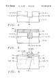
- FIGS. 1, 2 , 3 , 4 , 5 & 6 illustrate sequential sectional views of a raised source/drain MOSFET device with novel recessed gate.
- the present invention provides a method of forming a MOSFET device with raised source/drain relative to the gate dielectric.
- the process begins by forming a first insulating layer ( 12 ) over a silicon substrate ( 10 ).
- the first insulating layer ( 12 ) is preferably composed of silicon oxide (SiO 2 ) having a thickness in a range between about 70 ⁇ and 110 ⁇ with a target thickness of 100 ⁇ .
- the first insulating layer can be formed using a chemical vapor deposition process (CVD) or preferably using a thermal oxidation process as is well known in the art.
- a first barrier layer ( 14 ) is formed over the first insulating layer ( 12 ).
- the first barrier layer ( 14 ) can be composed of silicon nitride (Si 3 N 4 ) or silicon oxynitride (SiON).
- the first barrier layer ( 14 ) is preferably composed of silicon nitride having a thickness in the range between about 1500 ⁇ and 2500 ⁇ . The combined thickness of first insulating layer ( 12 ) and the first barrier layer ( 14 ) determining the height of the polysilicon gate to be formed during future processing.
- the silicon nitride layer can be formed by reacting silane and ammonia at atmospheric pressure at 700° C. to 900° C., or by reacting dichlorosilane and ammonia at reduced pressure at approximately 700° C. (LPCVD). Also, silicon nitride can be formed by plasma enhanced chemical vapor deposition by reacting silane with ammonia or nitrogen in a glow discharge between 200° C. and 350° C.
- the first nitride layer is preferably formed using a LPCVD process.
- a photoresist mask ( 16 ) is formed over the first barrier layer ( 14 ).
- the photoresist mask ( 16 ) is patterned using conventional photolithography as is well known in the art.
- the photoresist mask ( 16 ) is patterned to form a first opening ( 20 ) defining a gate area.
- the first barrier layer ( 14 ) and the first insulating layer ( 12 ) are removed through the first opening ( 20 ) by dry etching.
- the dry etch also forms a trench ( 50 ) in the silicon substrate ( 10 ) in the area of the first opening ( 20 ).
- This etch can be performed using CF 4 +O 2 as the source gas in the “plasma etch” mode. Alternately, the etch can be performed by changing the reaction gasses (e.g. etch SiN stopping on SiO, etch SiO stopping on Si, then use a timed etch for Si).
- the trench ( 50 ) in the substrate ( 10 ) is etched to a depth between about 0.05 ⁇ m and 0.07 ⁇ m, with a target of 0.6 ⁇ m.
- the photoresist mask ( 16 ) is removed. Then a lining oxide layer ( 52 ) is formed in the trench ( 50 ), and ions are implanted into the substrate ( 10 ).
- the lining oxide layer can be formed by thermal oxidation or preferably by CVD, having a thickness in a range between about 50 ⁇ and 200 ⁇ . Ions are implanted through the lining oxide layer ( 52 ) into the substrate ( 10 ) in the trench ( 50 ) to form anti-punch through (APT) ( 53 ) and threshhold voltage adjust (VT) ( 55 ).
- ions are implanted at an energy of between about 70 KeV and 100 KeV at a dose of between about 1.0E13 atm/cm 2 and 3.0E13 atm/cm 2 .
- “As” ions are implanted at an energy of between about 200 KeV and 250 KeV at a dose of between about 1.0E13 atm/cm 2 and 2.0E13 atm/cm 2
- “P” ions are implanted at an energy between about 120 KeV and 140 KeV at a dose between about 1.0E13 atm/cm 2 and 2.0E13 atm/cm 2 .
- the APT is preferably implanted at a depth between 2000 ⁇ and 2500 ⁇ .
- “B” ions are implanted at an energy between about 20 KeV and 30 KeV at a dose of between 2.0E12 atm/cm 2 and 5.0E12 atm/cm 2 .
- “As” ions are implanted at an energy of between 40 KeV and 50 KeV at a dose of between about 2.0E12 atm/cm 2 and 5.0 atm/cm 2 .
- the lining oxide layer ( 52 ) is removed. Typically the lining oxide layer is removed by a wet etch. An optional second sacrificial oxide layer ( 60 ) can be formed then removed to round sharp corners in the substrate ( 10 ) at the bottom of the trench ( 50 ).
- a gate oxide layer ( 62 ) is formed in the trench ( 50 ) on the substrate ( 10 ).
- the gate oxide is preferably formed to a thickness in a range between 32 ⁇ and 50 ⁇ by thermal oxidation in an oxygen-steam ambient, at a temperature between about 850° C. and 1000° C.
- a polysilicon layer ( 64 ) is formed on the gate oxide layer ( 62 ) and the barrier layer ( 14 ).
- the polysilicon layer is preferably formed by LPCVD, at a temperature between about 600° C. and 800° C. to a thickness in a range between 3000 ⁇ and 5000 ⁇ .
- the polysilicon layer ( 64 ) is planarized using a chemical mechanical polishing process (CMP).
- CMP is conducted to a point of stopping on the top surface of the barrier layer ( 14 ) to form a novel recessed gate ( 64 A) having a thickness of between about 2000 ⁇ and 3000 ⁇ .
- the recessed gate has sidewalls and a top.
- the barrier layer ( 14 ) is removed by an etching process selective to silicon nitride over polysilicon.
- the first insulating layer ( 12 ) is removed by an etching process selective to silicon dioxide over polysilicon and silicon.
- lightly doped source/drain regions ( 66 ) are formed by ion implantation.
- the implant ions are preferably arsenic, implanted at an energy in a range between about 15 KeV and 30 KeV, at a dose in a range between about 5.0E14 atm/cm 2 and 1.0E15 atm/cm 2 for an N-type LDD.
- boron ions are preferably implanted at an energy in a range between about 10 KeV and 25 KeV, at a dose in a range between about 1.0E14 atm/cm 2 and 3.0E14 atm/cm 2 .
- the LDD regions can be implanted deeper than than in conventional ultra-shallow juntion devices to a depth in a range between 1200 ⁇ and 1500 ⁇ , thereby reducing resistance without adverse short channel effects or reduced breakdown voltage.
- the inventors have determined that for a LDD, a shallow junction depth of 0.06 ⁇ m to 0.08 ⁇ m is necessary for short channel effect suppression. Since the gate region is recessed a depth of about 0.06 ⁇ m in the present invention, the shallow junction depth can be increased to between about 0.12 ⁇ m and 0.14 ⁇ m.
- spacers ( 68 ) are formed on the sidewalls of the recessed gate ( 64 A).
- the spacers are preferably composed of silicon oxide at a thickness in a range between 1000 ⁇ and 1500 ⁇ .
- the spacers can be formed using a LPCVD process or using a plasma enhanced chemical vapor deposition (PECVD) process at a temperature between about 300° C. and 800° C. after a LPCVD layer about 100 ⁇ thick is formed.
- the spacers are formed by an anisotropic reactive ion etch (REI) selective to silicon oxide over polysilicon, such as CHF 3 or CF 4 —O 2 .
- the spacers ( 68 ) can be composed of silicon nitride, formed to a thickness between 1000 ⁇ and 1500 ⁇ using a LPCVD process and anisotropically etching.
- Source/Drain regions ( 70 ) are formed adjacent to the spacers ( 68 ) by ion implantation.
- the implant ions are preferably As ions, implanted at an energy in a range between about 40 KeV and 70 KeV, at a dose in the range between about 3.0E15 and 5.5E15 atm/cm 2 or B ions, implanted at an energy in the range between about 3.0 KeV and 5.0 KeV, at a dose in a range between about 3.0E15 and 5.5E15 atm/cm 2 .
- Silicide layers ( 72 , 74 ) are formed on the source/drain regions ( 70 ) and on the top of the recessed gate ( 64 A) using a salicide process. Surfaces are cleaned using a hydrofluoric acid treatment. Titanium is deposited to a thickness in a range between about 250 ⁇ and 350 ⁇ using a sputtering process. The titanium caused to react with exposed polysilicon using a rapid thermal anneal (RTA) process at a temperature between about 550° C. and 700° C., for a period of time in a range between about 10 and 30 seconds. Unreacted titanium is removed using a solution of H 2 O 2 —H 2 SO 4 .
- RTA rapid thermal anneal
Abstract
The present invention provides a method for fabricating elevated and drain structures on a substrate. A first insulating layer is formed over a silicon substrate. A first barrier layer is formed over the first insulating layer. The first barrier layer, the first insulating layer and the substrate are patterned to form a trench. Ions are implanted into the substrate in the trench. A gate oxide layer is formed on the substrate in the trench. A polysilicon layer is deposited over the gate oxide layer and the barrier layer. The polysilicon layer is planarized using a chemical mechanical polishing process (CMP) stopping on the barrier layer to form a novel recessed gate. The barrier layer and the first insulating layer are removed. Lightly doped source/drain regions (LDD) are formed adjacent to the recessed gate. Spacers are formed on the sidewalls of the recessed gate. Source and drain regions are formed adjacent to the spacers. Salicide layers are formed on the source and drain regions and on the top of the recessed gate.
Description
1) Field of the Invention
This invention relates generally to fabrication of semiconductor devices and more particularly to the fabrication of elevated source and drain structures.
2) Description of the Prior Art
Under current MOSFET technology, raised source/drain regions are used in order to provide a transister having ultra-shallow junctions. Short channel effects increase as the source/drain depth increases, with respect to the gate oxide/silicon substrate interface. In order to minimize the source/drain depth raised source/drain regions are formed, typically using an epitaxial silicon process. The epitaxial growth of raised source/drain regions in MOSFET fabrication gives rise to numerous problems. The epitaxial growth of source and drain regions leaves facets or voids at the interfaces with the spacers formed adjacent to the gate and the interfaces with the field oxide regions. During the salicide process, silicide spikes are formed into these facets causing junction leakage. Another problem with the epitaxial growth of raised source/drain regions is diffusion of junction or lightly doped drain region (LDD) impurities during epitaxial growth. Yet another problem with epitaxial growth of raised source/drain regions is poor robustness and process yield due to difficulty controlling the thickness of the epitaial layer. Finally, the epitaxial growth of raised source/drain regions is an expensive process.
An alternative approach is disclosed by U.S. Pat. Nos. 5,079,180 & 5,198,378 (Rodder), whereby a thin spacer is formed adacent to the gate to allow for ion implant (I/I) after epitaxial growth of raised source/drain regions, while still allowing for sufficient horizontal migration of impurity ions to underlap the gate oxide. These patents also discloses formation of additional spacers in the abovementioned facets. This process does not solve the robustness issue caused by poor control of the thickness of the epitaxial layer nor does it alleviate the expense of epitaxial growth of raised source/drain regions. Also, this process relies on a timed etch in forming the additional spacers, again introducing a robustness issue as this process is also difficult to control.
Another alternative approach is disclosed by U.S. Pat. No. 5,312,768 (Gonzolez), whereby a layer of titanium nitride is deposited over the source/drain regions which acts as a barrier to impurity (phospherous or boron) outdiffusion. However, this process requires additional photo masks and a sputtering process which are expensive and complicated and reduce yields.
Yet another alternative approach is disclosed by U.S. Pat. No. 5,672,530 (Hsu), whereby raised polycrystalline silicon regions are deposited on previously deposited insulating layers, however this process is complicated and expensive due to numerous photo masking and etching steps. Also, the multiple photo masking and etching steps cause control and yield problems.
Alternatively, U.S. Pat. No. 5,641,694 (Kenney) shows a SIO transistor formed in a trench with the source and drain regions on the sidewalls.
U.S. Pat. No. 5,049,515 (Tzeng) shows an EEPROM having a drain region formed in a trench.
The importance of overcoming the various deficiencies noted above is evidenced by the extensive technological development directed to the subject, as documented by the relevant patent and technical literature. The closest and apparently more relevant technical developments in the patent literature can be gleaned by considering the aforementioned US patents.
It is an object of the present invention to acheive the performance advantages of ultra-shallow juntions in MOSFET devices.
It is another object of the present invention to reduce or eliminate juntion leakage problems associated with the salicide process on devices having ultra-shallow junctions.
It is another object of the present invention to reduce or eliminate the impurity ion diffusion problem associated with an epitaxial process.
It is another object of the present invention to eliminate the need for pre-amorpization of the polysilicon in the source/drain regions.
It is another object of the present invention to provide an economical and robust process for manufacturing MOSFET devices.
It is yet another object of the present invention to reduce resistance by implanting deeper LDD region while maintaining the performance advantages of ultra-shallow junctions.
To accomplish the above objectives, the present invention provides a method for fabricating elevated and drain structures on a substrate. The process begins by forming a first insulating layer (12) over a silicon substrate (10). A first barrier layer (14) is formed over the first insulating layer (12). A photoresist mask (16) having a first opening (20) is formed over the first barrier layer (14). The first barrier layer (14), the first insulating layer (12) and the silicon substrate (10) are dry etched through the first opening (20) in the photoresist mask (16) to form a trench (50) having the silicon substrate (10) as its bottom surface. Ions are implanted into the substrate (10) in the trench (50). Optionally, a second sacrificial oxide layer (60) can be formed, then removed to round sharp corners in the substrate (10) in the trench (50). A gate oxide layer (62) is formed on the substrate (10) in the trench (50). A polysilicon layer (64) is formed over the gate oxide layer (62) and the barrier layer (14). The polysilicon layer (64) is planarized using a chemical mechanical polishing process (CMP) to form a novel recessed gate (64A). The barrier layer can act as a CMP stop. The barrier layer (14) is removed by a selective etching process. The first insulating layer (12) is removed by a selective etching process. Lightly doped source/drain regions (LDD) (66) are formed adjacent to the recessed gate (64A). Spacers (68) are formed on the sidewalls of the recessed gate (64A). Source and drain regions (70) are formed adjacent to the spacers (68). Salicide layers (72,74) are formed on the source and drain regions (70) and on the top of the recessed gate (64A).
The junction leak problem typical of salicided ultra-shallow juctions can be reduced because there are no voids in which salicide spikes can form into the substrate. In the prior art, epitaxial groxth of raised source/drain regions results in facets. In the present invention the source/drain are formed in the substrate, which is raised with respect to the gate because of the novel recessed gate.
By raising the source/drain regions with respect to the novel recessed gate, additional disadvantages of the epitaxial process are avoided. The impurity ion diffusion problem associated with an epitaxial process is reduced. The need for pre-amorpization of the polysilicon in the source/drain regions is eliminated. Additional, expensive, photo-masking steps and timed etching steps are avoided.
The novel recessed gate allows the present invention to reduce resistance by implanting thicker LDD regions while maintaining the performance advantages of ultra-shallow junctions. These thicker LDD regions allow a thicker silicide to be formed while still maintaining a sufficient distance between the silicide and the channel.
The present invention achieves these benefits in the context of known process technology. However, a further understanding of the nature and advantages of the present invention may be realized by reference to the latter portions of the specification and attached drawings. Additional objects and advantages of the invention will be set forth in the description that follows, and in part will be obvious from the description, or may be learned by practice of the invention. The objects and advantages of the invention may be realized and obtained by means of instrumentalities and combinations particularly pointed out in the appended claims.
The features and advantages of a semiconductor device according to the present invention and further details of a process of fabricating such a semiconductor device in accordance with the present invention will be more clearly understood from the following description taken in conjunction with the accompanying drawings in which like reference numerals designate similar or corresponding elements, regions and portions and in which:
FIGS. 1, 2, 3, 4 ,5 & 6 illustrate sequential sectional views of a raised source/drain MOSFET device with novel recessed gate.
The present invention will be described in detail with reference to the accompanying drawings. The present invention provides a method of forming a MOSFET device with raised source/drain relative to the gate dielectric.
Referring to FIG. 1, the process begins by forming a first insulating layer (12) over a silicon substrate (10). The first insulating layer (12) is preferably composed of silicon oxide (SiO2) having a thickness in a range between about 70 Å and 110 Å with a target thickness of 100 Å. The first insulating layer can be formed using a chemical vapor deposition process (CVD) or preferably using a thermal oxidation process as is well known in the art.
Still referring to FIG. 1, a first barrier layer (14) is formed over the first insulating layer (12). The first barrier layer (14) can be composed of silicon nitride (Si3N4) or silicon oxynitride (SiON). The first barrier layer (14) is preferably composed of silicon nitride having a thickness in the range between about 1500 Å and 2500 Å. The combined thickness of first insulating layer (12) and the first barrier layer (14) determining the height of the polysilicon gate to be formed during future processing.
The silicon nitride layer can be formed by reacting silane and ammonia at atmospheric pressure at 700° C. to 900° C., or by reacting dichlorosilane and ammonia at reduced pressure at approximately 700° C. (LPCVD). Also, silicon nitride can be formed by plasma enhanced chemical vapor deposition by reacting silane with ammonia or nitrogen in a glow discharge between 200° C. and 350° C. The first nitride layer is preferably formed using a LPCVD process.
As shown in FIG. 1, a photoresist mask (16) is formed over the first barrier layer (14). The photoresist mask (16) is patterned using conventional photolithography as is well known in the art. The photoresist mask (16) is patterned to form a first opening (20) defining a gate area.
Referring to FIG. 2, the first barrier layer (14) and the first insulating layer (12) are removed through the first opening (20) by dry etching. The dry etch also forms a trench (50) in the silicon substrate (10) in the area of the first opening (20). This etch can be performed using CF4+O2 as the source gas in the “plasma etch” mode. Alternately, the etch can be performed by changing the reaction gasses (e.g. etch SiN stopping on SiO, etch SiO stopping on Si, then use a timed etch for Si). The trench (50) in the substrate (10) is etched to a depth between about 0.05 μm and 0.07 μm, with a target of 0.6 μm.
Referring to FIG. 3, the photoresist mask (16) is removed. Then a lining oxide layer (52) is formed in the trench (50), and ions are implanted into the substrate (10). The lining oxide layer can be formed by thermal oxidation or preferably by CVD, having a thickness in a range between about 50 Å and 200 Å. Ions are implanted through the lining oxide layer (52) into the substrate (10) in the trench (50) to form anti-punch through (APT) (53) and threshhold voltage adjust (VT) (55). For an NAPT “B” ions are implanted at an energy of between about 70 KeV and 100 KeV at a dose of between about 1.0E13 atm/cm2 and 3.0E13 atm/cm2. For a PAPT, “As” ions are implanted at an energy of between about 200 KeV and 250 KeV at a dose of between about 1.0E13 atm/cm2 and 2.0E13 atm/cm2, or “P” ions are implanted at an energy between about 120 KeV and 140 KeV at a dose between about 1.0E13 atm/cm2 and 2.0E13 atm/cm2. The APT is preferably implanted at a depth between 2000 Å and 2500 Å. For VTN, “B” ions are implanted at an energy between about 20 KeV and 30 KeV at a dose of between 2.0E12 atm/cm2 and 5.0E12 atm/cm2. For VTP, “As” ions are implanted at an energy of between 40 KeV and 50 KeV at a dose of between about 2.0E12 atm/cm2 and 5.0 atm/cm2.
Referring to FIG. 4, the lining oxide layer (52) is removed. Typically the lining oxide layer is removed by a wet etch. An optional second sacrificial oxide layer (60) can be formed then removed to round sharp corners in the substrate (10) at the bottom of the trench (50).
Referring to FIG. 5, a gate oxide layer (62) is formed in the trench (50) on the substrate (10). The gate oxide is preferably formed to a thickness in a range between 32 Å and 50 Å by thermal oxidation in an oxygen-steam ambient, at a temperature between about 850° C. and 1000° C.
Still referring to FIG. 5, a polysilicon layer (64) is formed on the gate oxide layer (62) and the barrier layer (14). The polysilicon layer is preferably formed by LPCVD, at a temperature between about 600° C. and 800° C. to a thickness in a range between 3000 Å and 5000 Å.
Referring to FIG. 6, the polysilicon layer (64) is planarized using a chemical mechanical polishing process (CMP). The CMP is conducted to a point of stopping on the top surface of the barrier layer (14) to form a novel recessed gate (64A) having a thickness of between about 2000 Å and 3000 Å. The recessed gate has sidewalls and a top.
Still referring to FIG. 6, the barrier layer (14) is removed by an etching process selective to silicon nitride over polysilicon. The first insulating layer (12) is removed by an etching process selective to silicon dioxide over polysilicon and silicon.
Still referring to FIG. 6, lightly doped source/drain regions (LDD) (66) are formed by ion implantation. The implant ions are preferably arsenic, implanted at an energy in a range between about 15 KeV and 30 KeV, at a dose in a range between about 5.0E14 atm/cm2 and 1.0E15 atm/cm2 for an N-type LDD. For a P-type LDD, boron ions are preferably implanted at an energy in a range between about 10 KeV and 25 KeV, at a dose in a range between about 1.0E14 atm/cm2 and 3.0E14 atm/cm2. Because of the novel recessed gate (64A), the LDD regions can be implanted deeper than than in conventional ultra-shallow juntion devices to a depth in a range between 1200 Å and 1500 Å, thereby reducing resistance without adverse short channel effects or reduced breakdown voltage.
The inventors have determined that for a LDD, a shallow junction depth of 0.06 μm to 0.08 μm is necessary for short channel effect suppression. Since the gate region is recessed a depth of about 0.06 μm in the present invention, the shallow junction depth can be increased to between about 0.12 μm and 0.14 μm.
Still referring to FIG. 6, spacers (68) are formed on the sidewalls of the recessed gate (64A). The spacers are preferably composed of silicon oxide at a thickness in a range between 1000 Å and 1500 Å. The spacers can be formed using a LPCVD process or using a plasma enhanced chemical vapor deposition (PECVD) process at a temperature between about 300° C. and 800° C. after a LPCVD layer about 100 Å thick is formed. The spacers are formed by an anisotropic reactive ion etch (REI) selective to silicon oxide over polysilicon, such as CHF3 or CF4—O2. Alternatively, the spacers (68) can be composed of silicon nitride, formed to a thickness between 1000 Å and 1500Å using a LPCVD process and anisotropically etching.
Source/Drain regions (70) are formed adjacent to the spacers (68) by ion implantation. The implant ions are preferably As ions, implanted at an energy in a range between about 40 KeV and 70 KeV, at a dose in the range between about 3.0E15 and 5.5E15 atm/cm2 or B ions, implanted at an energy in the range between about 3.0 KeV and 5.0 KeV, at a dose in a range between about 3.0E15 and 5.5E15 atm/cm2.
Silicide layers (72,74) are formed on the source/drain regions (70) and on the top of the recessed gate (64A) using a salicide process. Surfaces are cleaned using a hydrofluoric acid treatment. Titanium is deposited to a thickness in a range between about 250 Å and 350 Å using a sputtering process. The titanium caused to react with exposed polysilicon using a rapid thermal anneal (RTA) process at a temperature between about 550° C. and 700° C., for a period of time in a range between about 10 and 30 seconds. Unreacted titanium is removed using a solution of H2O2—H2SO4.
While the invention has been particularly shown and described with reference to the preferred embodiments thereof, it will be understood by those skilled in the art that various changes in form and details may be made without departing from the spirit and scope of the invention.
Claims (12)
1. A method for fabricating elevated source and drain regions on a substrate comprising the steps of:
a) forming a first insulating layer over a silicon substrate and forming a first barrier layer over said first insulating layer;
b) patterning said barrier layer, said first insulating layer and said silicon substrate to form a trench;
c) forming a gate oxide layer on said substrate in said trench;
d) depositing a polysilicon layer over said gate oxide layer and said barrier layer;
e) planarizing said polysilicon layer using a chemical-mechanical polishing process; said chemical-mechanical polish stopping on said barrier layer to form a recessed gate; said recessed gate having sidewalls and a top;
f) removing all of said barrier layer and said first insulating layer; and
g) implanting impurity ions to form elevated source and drain regions adjacent to said recessed gate.
2. The method of claim 1 wherein said trench extends a depth of between 0.05 μm and 0.07 μm into said substrate.
3. The method of claim 1 which further includes prior to forming said gate oxide layer, forming and removing a second sacraficial oxide layer to round the corners of said trench.
4. The method of claim 1 which further includes prior to forming said source and drain regions forming lightly doped drain regions at a depth of between 1200 Å and 1500 Å below the top of the substrate surface.
5. A method for fabricating elevated source and drain structures on a substrate comprising the steps of:
a) forming a first insulating layer over a silicon substrate;
b) forming a first barrier layer over said first insulating layer;
c) forming a photoresist mask over said first barrier layer; said photoresist mask having a first opening;
d) dry etching said barrier layer, said first insulating layer and said silicon substrate through said photoresist mask to form a trench;
e) removing said photoresist mask;
f) forming a lining oxide layer on said substrate in said trench and implanting ions into said substrate;
g) removing said lining oxide layer;
h) forming a gate oxide layer on said substrate in said trench;
i) depositing a polysilicon layer over said gate oxide layer and said barrier layer;
j) planarizing said polysilicon layer using a chemical-mechanical polishing process; said chemical-mechanical polish stopping on said barrier layer to form a recessed gate; said recessed gate having sidewalls and a top;
k) removing all of said barrier layer by a selective etching process;
l) removing all of said first insulating layer by a selective etching process;
m) implanting impurity ions to form lightly doped source and drain regions adjacent to said recessed gate;
n) forming spacers on said sidewalls of said recessed gate; and
o) implanting impurity ions to form source and drain regions adjacent to said spacers.
6. The method of claim 5 wherein said trench extends a depth of between 0.05 μm and 0.07 μm into said substrate.
7. The method of claim 5 which further includes prior to forming said gate oxide layer, forming and removing a second sacraficial oxide layer to round the corners of said trench.
8. The method of claim 5 wherein said lightly doped source and drain regions are formed to a depth of between 1200 Å and 1500 Å.
9. The method of claim 5 wherein said lightly doped source and drain regions are formed by implanting As ions with an energy between 15 KeV and 30 KeV at a dose of between 5.0E14 atm/cm2 and 1.0E15 atm/cm2.
10. The method of claim 5 wherein said lightly doped source and drain regions are formed by implanting B ions with an energy between 10 KeV and 25 KeV at a dose of between 1.0E14 atm/cm2 and 3.0E14 atm/cm2.
11. The method of claim 5 which further includes forming silicide layers on said source and drain regions and on said top of said recessed gate.
12. A method for fabricating elevated source and drain structures on a substrate comprising the steps of:
a) forming a first insulating layer over a silicon substrate;
b) forming a first barrier layer over said first insulating layer;
c) forming a photoresist mask over said first barrier layer; said photoresist mask having a first opening;
d) dry etching said barrier layer, said first insulating layer and said silicon substrate through said photoresist mask to form a trench having a depth of between about 0.05 microns and 0.07 microns;
e) removing said photoresist mask;
f) forming a lining oxide layer on said substrate in said trench and implanting ions into said substrate;
g) removing said lining oxide layer;
h) forming a gate oxide layer on said substrate in said trench; said gate oxide layer having a thickness of between about 32 angstroms and 50 angstroms;
i) depositing a polysilicon layer over said gate oxide layer and said barrier layer;
j) planarizing said polysilicon layer using a chemical-mechanical polishing process; said chemical-mechanical polish stopping on said barrier layer to form a recessed gate having a thickness of between about 2000 angstroms and 3000 angstroms; said recessed gate having sidewalls and a top;
k) removing all of said barrier layer by a selective etching process;
l) removing said first insulating layer by a selective etching process;
m) implanting impurity ions to form lightly doped source and drain regions adjacent to said recessed gate;
n) forming spacers on said sidewalls of said recessed gate; and
o) implanting As ions with an energy between 15 KeV and 30 KeV at a dose of between 5.0E14 atm/cm2 and 1.0E15 atm/cm2 to form source and drain regions adjacent to said spacers; and
p) depositing a metal layer over said silicon substrate and annealing said metal layer to form silicide on said source and drain regions.
Priority Applications (1)
| Application Number | Priority Date | Filing Date | Title |
|---|---|---|---|
| US09/187,303 US6303448B1 (en) | 1998-11-05 | 1998-11-05 | Method for fabricating raised source/drain structures |
Applications Claiming Priority (1)
| Application Number | Priority Date | Filing Date | Title |
|---|---|---|---|
| US09/187,303 US6303448B1 (en) | 1998-11-05 | 1998-11-05 | Method for fabricating raised source/drain structures |
Publications (1)
| Publication Number | Publication Date |
|---|---|
| US6303448B1 true US6303448B1 (en) | 2001-10-16 |
Family
ID=22688431
Family Applications (1)
| Application Number | Title | Priority Date | Filing Date |
|---|---|---|---|
| US09/187,303 Expired - Lifetime US6303448B1 (en) | 1998-11-05 | 1998-11-05 | Method for fabricating raised source/drain structures |
Country Status (1)
| Country | Link |
|---|---|
| US (1) | US6303448B1 (en) |
Cited By (26)
| Publication number | Priority date | Publication date | Assignee | Title |
|---|---|---|---|---|
| US6368926B1 (en) * | 2000-03-13 | 2002-04-09 | Advanced Micro Devices, Inc. | Method of forming a semiconductor device with source/drain regions having a deep vertical junction |
| US6531380B2 (en) * | 2000-06-05 | 2003-03-11 | Chartered Semiconductor Manufacturing Ltd. | Method of fabricating T-shaped recessed polysilicon gate transistors |
| US6534370B2 (en) * | 2000-08-16 | 2003-03-18 | Hyundai Electronics Industries Co., Ltd. | Method for fabricating a semiconductor device having an elevated source/drain scheme |
| KR20030044339A (en) * | 2001-11-29 | 2003-06-09 | 주식회사 하이닉스반도체 | Method of manufacturing a transistor in a semiconductor device |
| US6693026B2 (en) * | 2000-08-01 | 2004-02-17 | Hynix Semiconductor Inc. | Semiconductor device and method for fabricating the same |
| US6716046B2 (en) | 1999-12-28 | 2004-04-06 | Intel Corporation | Field effect transistor structure with self-aligned raised source/drain extensions |
| US20040129959A1 (en) * | 2002-12-18 | 2004-07-08 | Seong-Ho Kim | Semiconductor devices with enlarged recessed gate electrodes and methods of fabrication therefor |
| US20050142823A1 (en) * | 2003-12-31 | 2005-06-30 | Dongbuanam Semiconductor Inc. | Method of fabricating gate electrode of semiconductor device |
| US20060049455A1 (en) * | 2004-09-09 | 2006-03-09 | Se-Myeong Jang | Semiconductor devices with local recess channel transistors and methods of manufacturing the same |
| US20060099752A1 (en) * | 2004-11-10 | 2006-05-11 | Advanced Micro Devices, Inc. | Strained fully depleted silicon on insulator semiconductor device and manufacturing method therefor |
| US20060124976A1 (en) * | 2004-12-15 | 2006-06-15 | International Business Machines Corporation | Recessed gate for an image sensor |
| US20060131658A1 (en) * | 2004-12-22 | 2006-06-22 | Dongbuanam Semiconductor Inc. | MOS device, CMOS device, and fabricating method thereof |
| US20060202259A1 (en) * | 2005-03-09 | 2006-09-14 | Yoshio Ozawa | Semiconductor device and method of fabricating the same |
| US20060211229A1 (en) * | 2005-03-18 | 2006-09-21 | Hynix Semiconductor Inc. | Method for fabricating semiconductor device |
| US20070007571A1 (en) * | 2005-07-06 | 2007-01-11 | Richard Lindsay | Semiconductor device with a buried gate and method of forming the same |
| US20070105295A1 (en) * | 2005-11-08 | 2007-05-10 | Dongbuanam Semiconductor Inc. | Method for forming lightly-doped-drain metal-oxide-semiconductor (LDD MOS) device |
| US20070152284A1 (en) * | 2005-12-29 | 2007-07-05 | Jeong Ho Park | Transistor device and method for manufacturing the same |
| US20070164354A1 (en) * | 2003-02-28 | 2007-07-19 | Samsung Electronics Co., Ltd. | MOS transistor with elevated source and drain structures and method of fabrication thereof |
| CN100342544C (en) * | 2001-12-31 | 2007-10-10 | 通用半导体公司 | High voltage power MOSFET includes doped columns |
| US7303965B2 (en) * | 1998-06-29 | 2007-12-04 | Kabushiki Kaisha Toshiba | MIS transistor and method for producing same |
| US7528427B2 (en) | 2007-01-30 | 2009-05-05 | International Business Machines Corporation | Pixel sensor cell having asymmetric transfer gate with reduced pinning layer barrier potential |
| US20090239346A1 (en) * | 2005-04-14 | 2009-09-24 | Samsung Electronics Co., Ltd. | Semiconductor device with finfet and method of fabricating the same |
| US20100013004A1 (en) * | 2008-07-16 | 2010-01-21 | Promos Technologies Inc. | Recessed channel transistor and method for preparing the same |
| CN103165427A (en) * | 2011-12-13 | 2013-06-19 | 中芯国际集成电路制造(上海)有限公司 | Metal oxide semiconductor (MOS) device and forming method thereof |
| US20150295066A1 (en) * | 2012-09-05 | 2015-10-15 | Commissariat A L'energie Atomique Et Aux Ene Alt | Process for producing fet transistors |
| US20230083560A1 (en) * | 2021-09-14 | 2023-03-16 | Sandisk Technologies Llc | Field effect transistors with gate fins and method of making the same |
Citations (23)
| Publication number | Priority date | Publication date | Assignee | Title |
|---|---|---|---|---|
| US4839306A (en) * | 1987-03-24 | 1989-06-13 | Oki Electric Industry Co., Ltd. | Method of manufacturing a trench filled with an insulating material in a semiconductor substrate |
| US5049515A (en) | 1990-03-09 | 1991-09-17 | Intel Corporation, Inc. | Method of making a three-dimensional memory cell with integral select transistor |
| US5079180A (en) | 1988-12-22 | 1992-01-07 | Texas Instruments Incorporated | Method of fabricating a raised source/drain transistor |
| US5198378A (en) | 1988-10-31 | 1993-03-30 | Texas Instruments Incorporated | Process of fabricating elevated source/drain transistor |
| US5312768A (en) | 1993-03-09 | 1994-05-17 | Micron Technology, Inc. | Integrated process for fabricating raised, source/drain, short-channel transistors |
| US5371024A (en) * | 1988-09-30 | 1994-12-06 | Kabushiki Kaisha Toshiba | Semiconductor device and process for manufacturing the same |
| US5434093A (en) * | 1994-08-10 | 1995-07-18 | Intel Corporation | Inverted spacer transistor |
| US5489543A (en) * | 1994-12-01 | 1996-02-06 | United Microelectronics Corp. | Method of forming a MOS device having a localized anti-punchthrough region |
| US5538913A (en) * | 1995-11-13 | 1996-07-23 | United Microelectronics Corporation | Process for fabricating MOS transistors having full-overlap lightly-doped drain structure |
| US5576227A (en) * | 1994-11-02 | 1996-11-19 | United Microelectronics Corp. | Process for fabricating a recessed gate MOS device |
| US5641694A (en) | 1994-12-22 | 1997-06-24 | International Business Machines Corporation | Method of fabricating vertical epitaxial SOI transistor |
| US5665619A (en) * | 1995-05-01 | 1997-09-09 | National Semiconductor Corporation | Method of fabricating a self-aligned contact trench DMOS transistor structure |
| US5672530A (en) | 1993-03-22 | 1997-09-30 | Sharp Microelectronics Technology, Inc. | Method of making MOS transistor with controlled shallow source/drain junction |
| US5736435A (en) * | 1995-07-03 | 1998-04-07 | Motorola, Inc. | Process for fabricating a fully self-aligned soi mosfet |
| US5801075A (en) * | 1996-10-30 | 1998-09-01 | Advanced Micro Devices, Inc. | Method of forming trench transistor with metal spacers |
| US5817558A (en) * | 1997-06-20 | 1998-10-06 | Acer Semiconductor Manufacturing Inc. | Method of forming a T-gate Lightly-Doped Drain semiconductor device |
| US5818098A (en) * | 1996-02-29 | 1998-10-06 | Motorola, Inc. | Semiconductor device having a pedestal |
| US5918132A (en) * | 1996-12-31 | 1999-06-29 | Intel Corporation | Method for narrow space formation and self-aligned channel implant |
| US5937297A (en) * | 1998-06-01 | 1999-08-10 | Chartered Semiconductor Manufacturing, Ltd. | Method for making sub-quarter-micron MOSFET |
| US5953602A (en) * | 1995-05-26 | 1999-09-14 | Lg Semicon Co., Ltd. | EEPROM cell and related method of making thereof |
| US5972754A (en) * | 1998-06-10 | 1999-10-26 | Mosel Vitelic, Inc. | Method for fabricating MOSFET having increased effective gate length |
| US5998288A (en) * | 1998-04-17 | 1999-12-07 | Advanced Micro Devices, Inc. | Ultra thin spacers formed laterally adjacent a gate conductor recessed below the upper surface of a substrate |
| US6025232A (en) * | 1997-11-12 | 2000-02-15 | Micron Technology, Inc. | Methods of forming field effect transistors and related field effect transistor constructions |
-
1998
- 1998-11-05 US US09/187,303 patent/US6303448B1/en not_active Expired - Lifetime
Patent Citations (23)
| Publication number | Priority date | Publication date | Assignee | Title |
|---|---|---|---|---|
| US4839306A (en) * | 1987-03-24 | 1989-06-13 | Oki Electric Industry Co., Ltd. | Method of manufacturing a trench filled with an insulating material in a semiconductor substrate |
| US5371024A (en) * | 1988-09-30 | 1994-12-06 | Kabushiki Kaisha Toshiba | Semiconductor device and process for manufacturing the same |
| US5198378A (en) | 1988-10-31 | 1993-03-30 | Texas Instruments Incorporated | Process of fabricating elevated source/drain transistor |
| US5079180A (en) | 1988-12-22 | 1992-01-07 | Texas Instruments Incorporated | Method of fabricating a raised source/drain transistor |
| US5049515A (en) | 1990-03-09 | 1991-09-17 | Intel Corporation, Inc. | Method of making a three-dimensional memory cell with integral select transistor |
| US5312768A (en) | 1993-03-09 | 1994-05-17 | Micron Technology, Inc. | Integrated process for fabricating raised, source/drain, short-channel transistors |
| US5672530A (en) | 1993-03-22 | 1997-09-30 | Sharp Microelectronics Technology, Inc. | Method of making MOS transistor with controlled shallow source/drain junction |
| US5434093A (en) * | 1994-08-10 | 1995-07-18 | Intel Corporation | Inverted spacer transistor |
| US5576227A (en) * | 1994-11-02 | 1996-11-19 | United Microelectronics Corp. | Process for fabricating a recessed gate MOS device |
| US5489543A (en) * | 1994-12-01 | 1996-02-06 | United Microelectronics Corp. | Method of forming a MOS device having a localized anti-punchthrough region |
| US5641694A (en) | 1994-12-22 | 1997-06-24 | International Business Machines Corporation | Method of fabricating vertical epitaxial SOI transistor |
| US5665619A (en) * | 1995-05-01 | 1997-09-09 | National Semiconductor Corporation | Method of fabricating a self-aligned contact trench DMOS transistor structure |
| US5953602A (en) * | 1995-05-26 | 1999-09-14 | Lg Semicon Co., Ltd. | EEPROM cell and related method of making thereof |
| US5736435A (en) * | 1995-07-03 | 1998-04-07 | Motorola, Inc. | Process for fabricating a fully self-aligned soi mosfet |
| US5538913A (en) * | 1995-11-13 | 1996-07-23 | United Microelectronics Corporation | Process for fabricating MOS transistors having full-overlap lightly-doped drain structure |
| US5818098A (en) * | 1996-02-29 | 1998-10-06 | Motorola, Inc. | Semiconductor device having a pedestal |
| US5801075A (en) * | 1996-10-30 | 1998-09-01 | Advanced Micro Devices, Inc. | Method of forming trench transistor with metal spacers |
| US5918132A (en) * | 1996-12-31 | 1999-06-29 | Intel Corporation | Method for narrow space formation and self-aligned channel implant |
| US5817558A (en) * | 1997-06-20 | 1998-10-06 | Acer Semiconductor Manufacturing Inc. | Method of forming a T-gate Lightly-Doped Drain semiconductor device |
| US6025232A (en) * | 1997-11-12 | 2000-02-15 | Micron Technology, Inc. | Methods of forming field effect transistors and related field effect transistor constructions |
| US5998288A (en) * | 1998-04-17 | 1999-12-07 | Advanced Micro Devices, Inc. | Ultra thin spacers formed laterally adjacent a gate conductor recessed below the upper surface of a substrate |
| US5937297A (en) * | 1998-06-01 | 1999-08-10 | Chartered Semiconductor Manufacturing, Ltd. | Method for making sub-quarter-micron MOSFET |
| US5972754A (en) * | 1998-06-10 | 1999-10-26 | Mosel Vitelic, Inc. | Method for fabricating MOSFET having increased effective gate length |
Cited By (52)
| Publication number | Priority date | Publication date | Assignee | Title |
|---|---|---|---|---|
| US7303965B2 (en) * | 1998-06-29 | 2007-12-04 | Kabushiki Kaisha Toshiba | MIS transistor and method for producing same |
| US6716046B2 (en) | 1999-12-28 | 2004-04-06 | Intel Corporation | Field effect transistor structure with self-aligned raised source/drain extensions |
| US6956263B1 (en) * | 1999-12-28 | 2005-10-18 | Intel Corporation | Field effect transistor structure with self-aligned raised source/drain extensions |
| US6368926B1 (en) * | 2000-03-13 | 2002-04-09 | Advanced Micro Devices, Inc. | Method of forming a semiconductor device with source/drain regions having a deep vertical junction |
| US6531380B2 (en) * | 2000-06-05 | 2003-03-11 | Chartered Semiconductor Manufacturing Ltd. | Method of fabricating T-shaped recessed polysilicon gate transistors |
| US6693026B2 (en) * | 2000-08-01 | 2004-02-17 | Hynix Semiconductor Inc. | Semiconductor device and method for fabricating the same |
| US6534370B2 (en) * | 2000-08-16 | 2003-03-18 | Hyundai Electronics Industries Co., Ltd. | Method for fabricating a semiconductor device having an elevated source/drain scheme |
| KR20030044339A (en) * | 2001-11-29 | 2003-06-09 | 주식회사 하이닉스반도체 | Method of manufacturing a transistor in a semiconductor device |
| CN100342544C (en) * | 2001-12-31 | 2007-10-10 | 通用半导体公司 | High voltage power MOSFET includes doped columns |
| US7148527B2 (en) | 2002-12-18 | 2006-12-12 | Samsung Electronics Co., Ltd. | Semiconductor devices with enlarged recessed gate electrodes |
| US20090215238A1 (en) * | 2002-12-18 | 2009-08-27 | Samsung Electronics Co., Ltd. | Methods of fabricating semiconductor devices with enlarged recessed gate electrodes |
| US7541656B2 (en) | 2002-12-18 | 2009-06-02 | Samsung Electronics Co., Ltd. | Semiconductor devices with enlarged recessed gate electrodes |
| US20040129959A1 (en) * | 2002-12-18 | 2004-07-08 | Seong-Ho Kim | Semiconductor devices with enlarged recessed gate electrodes and methods of fabrication therefor |
| US7871914B2 (en) | 2002-12-18 | 2011-01-18 | Samsung Electronics Co., Ltd. | Methods of fabricating semiconductor devices with enlarged recessed gate electrodes |
| US20070057288A1 (en) * | 2002-12-18 | 2007-03-15 | Samsung Electronics., Ltd. | Methods of Fabricating Semiconductor Devices with Enlarged Recessed Gate Electrodes |
| US20070164373A1 (en) * | 2003-02-28 | 2007-07-19 | Samsung Electronics Co., Ltd. | MOS transistor with elevated source and drain structures and method of fabrication thereof |
| US20070164354A1 (en) * | 2003-02-28 | 2007-07-19 | Samsung Electronics Co., Ltd. | MOS transistor with elevated source and drain structures and method of fabrication thereof |
| US20050142823A1 (en) * | 2003-12-31 | 2005-06-30 | Dongbuanam Semiconductor Inc. | Method of fabricating gate electrode of semiconductor device |
| US7211491B2 (en) * | 2003-12-31 | 2007-05-01 | Dongbu Electronics Co., Ltd. | Method of fabricating gate electrode of semiconductor device |
| US20090291541A1 (en) * | 2004-09-09 | 2009-11-26 | Samsung Electronics Co., Ltd. | Methods of manufacturing semiconductor devices with local recess channel transistors |
| US7842572B2 (en) | 2004-09-09 | 2010-11-30 | Samsung Electronics Co., Ltd. | Methods of manufacturing semiconductor devices with local recess channel transistors |
| US7586150B2 (en) | 2004-09-09 | 2009-09-08 | Samsung Electronic Co., Ltd. | Semiconductor devices with local recess channel transistors and methods of manufacturing the same |
| US20060049455A1 (en) * | 2004-09-09 | 2006-03-09 | Se-Myeong Jang | Semiconductor devices with local recess channel transistors and methods of manufacturing the same |
| US8502283B2 (en) | 2004-11-10 | 2013-08-06 | Globalfoundries Inc. | Strained fully depleted silicon on insulator semiconductor device |
| US20060099752A1 (en) * | 2004-11-10 | 2006-05-11 | Advanced Micro Devices, Inc. | Strained fully depleted silicon on insulator semiconductor device and manufacturing method therefor |
| US7306997B2 (en) | 2004-11-10 | 2007-12-11 | Advanced Micro Devices, Inc. | Strained fully depleted silicon on insulator semiconductor device and manufacturing method therefor |
| US7217968B2 (en) * | 2004-12-15 | 2007-05-15 | International Business Machines Corporation | Recessed gate for an image sensor |
| US20070184614A1 (en) * | 2004-12-15 | 2007-08-09 | International Business Machines Corporation | Recessed gate for a cmos image sensor |
| US20060124976A1 (en) * | 2004-12-15 | 2006-06-15 | International Business Machines Corporation | Recessed gate for an image sensor |
| US7572701B2 (en) | 2004-12-15 | 2009-08-11 | International Business Machines Corporation | Recessed gate for a CMOS image sensor |
| US20060131658A1 (en) * | 2004-12-22 | 2006-06-22 | Dongbuanam Semiconductor Inc. | MOS device, CMOS device, and fabricating method thereof |
| US20060202259A1 (en) * | 2005-03-09 | 2006-09-14 | Yoshio Ozawa | Semiconductor device and method of fabricating the same |
| US20090269894A1 (en) * | 2005-03-09 | 2009-10-29 | Kabushiki Kaisha Toshiba | Semiconductor device and method of fabricating the same cross-reference to related applications |
| US8026133B2 (en) | 2005-03-09 | 2011-09-27 | Kabushiki Kaisha Toshiba | Method of fabricating a semiconductor device with a non-uniform gate insulating film |
| US20060211229A1 (en) * | 2005-03-18 | 2006-09-21 | Hynix Semiconductor Inc. | Method for fabricating semiconductor device |
| US7332397B2 (en) * | 2005-03-18 | 2008-02-19 | Hynix Semiconductor Inc. | Method for fabricating semiconductor device |
| US7972914B2 (en) * | 2005-04-14 | 2011-07-05 | Samsung Electronics Co., Ltd. | Semiconductor device with FinFET and method of fabricating the same |
| US20090239346A1 (en) * | 2005-04-14 | 2009-09-24 | Samsung Electronics Co., Ltd. | Semiconductor device with finfet and method of fabricating the same |
| US8796762B2 (en) | 2005-07-06 | 2014-08-05 | Infineon Technologies Ag | Buried gate transistor |
| US20070007571A1 (en) * | 2005-07-06 | 2007-01-11 | Richard Lindsay | Semiconductor device with a buried gate and method of forming the same |
| US9059141B2 (en) | 2005-07-06 | 2015-06-16 | Infineon Technologies Ag | Buried gate transistor |
| US8338887B2 (en) * | 2005-07-06 | 2012-12-25 | Infineon Technologies Ag | Buried gate transistor |
| US20070105295A1 (en) * | 2005-11-08 | 2007-05-10 | Dongbuanam Semiconductor Inc. | Method for forming lightly-doped-drain metal-oxide-semiconductor (LDD MOS) device |
| US7427546B2 (en) * | 2005-12-29 | 2008-09-23 | Dongbu Hitek Co., Ltd. | Transistor device and method for manufacturing the same |
| US20070152284A1 (en) * | 2005-12-29 | 2007-07-05 | Jeong Ho Park | Transistor device and method for manufacturing the same |
| US7528427B2 (en) | 2007-01-30 | 2009-05-05 | International Business Machines Corporation | Pixel sensor cell having asymmetric transfer gate with reduced pinning layer barrier potential |
| US20100013004A1 (en) * | 2008-07-16 | 2010-01-21 | Promos Technologies Inc. | Recessed channel transistor and method for preparing the same |
| US7781830B2 (en) | 2008-07-16 | 2010-08-24 | Promos Technologies Inc. | Recessed channel transistor and method for preparing the same |
| CN103165427A (en) * | 2011-12-13 | 2013-06-19 | 中芯国际集成电路制造(上海)有限公司 | Metal oxide semiconductor (MOS) device and forming method thereof |
| US20150295066A1 (en) * | 2012-09-05 | 2015-10-15 | Commissariat A L'energie Atomique Et Aux Ene Alt | Process for producing fet transistors |
| US11264479B2 (en) * | 2012-09-05 | 2022-03-01 | Commissariat A L'energie Atomique Et Aux Energies Alternatives | Process for producing FET transistors |
| US20230083560A1 (en) * | 2021-09-14 | 2023-03-16 | Sandisk Technologies Llc | Field effect transistors with gate fins and method of making the same |
Similar Documents
| Publication | Publication Date | Title |
|---|---|---|
| US6303448B1 (en) | Method for fabricating raised source/drain structures | |
| US5856225A (en) | Creation of a self-aligned, ion implanted channel region, after source and drain formation | |
| EP0480446B1 (en) | Method of fabricating a high-performance insulated-gate-field-effect transistor and transistor fabricated by it | |
| US6309933B1 (en) | Method of fabricating T-shaped recessed polysilicon gate transistors | |
| US5972754A (en) | Method for fabricating MOSFET having increased effective gate length | |
| US7541244B2 (en) | Semiconductor device having a trench gate and method of fabricating the same | |
| US6090691A (en) | Method for forming a raised source and drain without using selective epitaxial growth | |
| US6917085B2 (en) | Semiconductor transistor using L-shaped spacer | |
| US6300201B1 (en) | Method to form a high K dielectric gate insulator layer, a metal gate structure, and self-aligned channel regions, post source/drain formation | |
| US6063677A (en) | Method of forming a MOSFET using a disposable gate and raised source and drain | |
| US5766998A (en) | Method for fabricating narrow channel field effect transistors having titanium shallow junctions | |
| JP2735041B2 (en) | Semiconductor device and manufacturing method thereof | |
| US6214670B1 (en) | Method for manufacturing short-channel, metal-gate CMOS devices with superior hot carrier performance | |
| JPH06163571A (en) | Insulated-gate field-effect transistor and its manufacture | |
| US6924180B2 (en) | Method of forming a pocket implant region after formation of composite insulator spacers | |
| EP0522991A1 (en) | Inverse T-gate FET transistor | |
| US6506649B2 (en) | Method for forming notch gate having self-aligned raised source/drain structure | |
| US8088666B2 (en) | Semiconductor device manufacture method including process of implanting impurity into gate electrode independently from source/drain and semiconductor device manufactured by the method | |
| JPH10135482A (en) | Formation of mosfet using disposable gate having sidewall dielectric | |
| US6326272B1 (en) | Method for forming self-aligned elevated transistor | |
| US20040219724A1 (en) | Methods of fabricating MOS field effect transistors with pocket regions | |
| US5702986A (en) | Low-stress method of fabricating field-effect transistors having silicon nitride spacers on gate electrode edges | |
| US6969646B2 (en) | Method of activating polysilicon gate structure dopants after offset spacer deposition | |
| US5915181A (en) | Method for forming a deep submicron MOSFET device using a silicidation process | |
| US6093593A (en) | Method of forming a gate which provides a reduced corner recess in adjacent shallow trench isolation |
Legal Events
| Date | Code | Title | Description |
|---|---|---|---|
| AS | Assignment |
Owner name: TAIWAN SEMICONDUCTOR MANUFACTURING COMPANY, TAIWAN Free format text: ASSIGNMENT OF ASSIGNORS INTEREST;ASSIGNORS:CHANG, SHOU-ZEN;TSAI, CHAO-CHIEH;REEL/FRAME:009574/0176 Effective date: 19980810 |
|
| STCF | Information on status: patent grant |
Free format text: PATENTED CASE |
|
| FPAY | Fee payment |
Year of fee payment: 4 |
|
| FPAY | Fee payment |
Year of fee payment: 8 |
|
| FPAY | Fee payment |
Year of fee payment: 12 |