US6332179B1 - Allocation for back-to-back misses in a directory based cache - Google Patents
Allocation for back-to-back misses in a directory based cache Download PDFInfo
- Publication number
- US6332179B1 US6332179B1 US09/377,636 US37763699A US6332179B1 US 6332179 B1 US6332179 B1 US 6332179B1 US 37763699 A US37763699 A US 37763699A US 6332179 B1 US6332179 B1 US 6332179B1
- Authority
- US
- United States
- Prior art keywords
- memory
- cache
- address
- directory
- data
- Prior art date
- Legal status (The legal status is an assumption and is not a legal conclusion. Google has not performed a legal analysis and makes no representation as to the accuracy of the status listed.)
- Expired - Fee Related
Links
Images


Classifications
-
- G—PHYSICS
- G06—COMPUTING; CALCULATING OR COUNTING
- G06F—ELECTRIC DIGITAL DATA PROCESSING
- G06F12/00—Accessing, addressing or allocating within memory systems or architectures
- G06F12/02—Addressing or allocation; Relocation
- G06F12/08—Addressing or allocation; Relocation in hierarchically structured memory systems, e.g. virtual memory systems
- G06F12/0802—Addressing of a memory level in which the access to the desired data or data block requires associative addressing means, e.g. caches
- G06F12/0844—Multiple simultaneous or quasi-simultaneous cache accessing
- G06F12/0855—Overlapped cache accessing, e.g. pipeline
- G06F12/0859—Overlapped cache accessing, e.g. pipeline with reload from main memory
-
- G—PHYSICS
- G06—COMPUTING; CALCULATING OR COUNTING
- G06F—ELECTRIC DIGITAL DATA PROCESSING
- G06F12/00—Accessing, addressing or allocating within memory systems or architectures
- G06F12/02—Addressing or allocation; Relocation
- G06F12/08—Addressing or allocation; Relocation in hierarchically structured memory systems, e.g. virtual memory systems
- G06F12/0802—Addressing of a memory level in which the access to the desired data or data block requires associative addressing means, e.g. caches
- G06F12/0864—Addressing of a memory level in which the access to the desired data or data block requires associative addressing means, e.g. caches using pseudo-associative means, e.g. set-associative or hashing
Definitions
- the present invention relates to the field of memory management in a data processing system such as a computer. More specifically, the present invention relates to a system and method for controlling allocation of memory in a cache memory to maximize storage use and minimizes retries.
- microprocessors have created many challenges. As components are more densely packed on a microprocessor, the processor's speed of operation increases. In addition, techniques such as pipelining and multiple processor systems have created processing systems with very large data throughput needs. To meet this challenge, system designers have turned to cache memory systems.
- Cache memory systems rely on the principle of locality of The locality of references principle states that a computer program will spend approximately ninety percent of its time accessing ten percent of its code. In addition, the next memory address accessed is usually an address near the last address accessed. Using these principles, a small portion of the memory may be fetched into a small, extremely fast memory called a cache. Using the principle of locality of references, data with a high probability of being accessed by the processor is stored in the cache. Thus, the processor retrieves the data directly from the very fast cache memory. This means that the processor will spend as little time as possible waiting for the necessary data from memory.
- the development of cache systems has reached a very high level of sophistication. It is common in microprocessor-based systems to have two or more levels of cache. Often, the first level (L1) of cache is formed on same semiconductor substrate as the microprocessor. This provides maximum throughput between the first level cache and the processor. The second level (L2) cache is often a larger memory, which may be external or internal. The L2 cache provides a larger, but slower, data storage capability.
- a particular problem occurs when a miss occurs on two pipelined accesses.
- a cache miss occurs when a processor requests memory that is not stored in the cache and must be fetched from slower memory devices.
- a common technique is to allocate a way or write set for the missing data upon the first detection of a cache miss. The memory system then fetches the missed data block from system memory or a lower level cache and stores it in the allocated write set.
- a memory caching system that uses a method for allocating blocks of memory by: determining if the contents at a selected memory address are stored in the cache by comparing the selected memory address to the addresses stored in the tags, if the selected memory address is not in the cache, allocating a place in the directory for selected address, wherein, if a place in the directory for an address having the same cache line as the selected memory address has been previously allocated or is in the process of allocating, the selected memory address is allocated to the location of the previous or pending allocation.
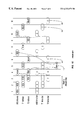
- FIG. 1 is a block diagram showing the interaction of components in a simplified computing system involving cache memories
- FIG. 2 is a block diagram showing the internal components of cache 14 ;
- FIG. 3 is a schematic diagram showing the system for determining if a tag for addressed data is stored in the cache
- FIG. 4 is a chart showing the different components of a data address
- FIG. 5 is a chart showing the organization of one way of directory 30 ;
- FIG. 6 is a chart showing the organization of one way of memory array 26 ;
- FIG. 7 is a logic diagram of the address pipeline of cache 14 ;
- FIG. 8 is a logic diagram of the write set pipeline of cache 14 ;
- FIG. 9 is a timing diagram showing the steps involved in a prior art system which lead to the misallocation of cache memory write sets
- FIG. 10 is another timing diagram showing another prior art system that avoids misallocation, but imposes a performance penalty, by blocking allocation and forcing a retry.
- FIG. 11 is a timing diagram showing the operation of the present invention, which prevents the misallocation of cache memory write sets and avoids a performance penalty.
- FIG. 1 is a block diagram showing a simplified computing system including a preferred embodiment of the present invention.
- System 10 is a computing system using a two level cache system.
- Processor 12 communicates with caches 13 and 14 to write and read information from the memory system of the computer.
- Cache 14 is in communication with address bus 16 and data bus 18 .
- Address bus 16 and data bus 18 provide system control and data flow, respectively, for system 10 .
- Memory controller 20 is in communication with address bus 16 and data bus 18 .
- Memory controller 20 provides control of the flow to and from system memory 22 .
- system memory 22 consists of dynamic random access memory (DRAM).
- DRAM provides high data capacity but is slower than static random access memory (SRAM).
- SRAM is generally the type of memory used in cache memories because of its greater speed and relatively efficient use of power.
- I/O controller 24 provides communication between address bus 16 , data bus 18 and input/output devices such as a disk drive storage device, a video controller, a keyboard, etc.
- Cache 13 and cache 14 are shown in this embodiment as a two-level cache memory.
- Single level cache memory systems may advantageously use the present invention.
- This type of cache is known as level one (L1) cache. Higher level caches provide greater storage capacity at somewhat diminished access speeds. If requested data is not found in the L1 cache, it can be rapidly accessed from the level two (L2) or three (L3) cache. Thus, the performance penalty for a cache miss at the L1 cache is minimized because of the high-speed access available from the L2 or L3 caches.
- FIG. 2 is a block diagram showing the internal structure of cache memory 14 .
- Data is stored in memory array 26 .
- Data communication with data bus 18 and processor 12 occurs via I/O buffer 28 .
- Cache memory 14 is a conventional single port (single I/O) memory. Dual port memories may be advantageously used for higher I/O throughput, but their use adds considerable system complexity.
- Directory 30 stores addressing and control information for the data stored in array 26 . Data is addressed and accessed by cache controller 32 , which accepts addresses from address bus 16 and processor 12 . Controller 32 determines what is stored in array 26 , directory 30 and where it is stored. It also determines what data will be discarded and when a system memory fetch is necessary.
- FIG. 3 is a schematic diagram showing the interaction of the directory 30 and the data array 26 in cache 14 .
- the memory of cache 14 is an eight way associative cache. Both directory 30 and data array 26 are organized into eight ways (Way0-Way7).
- Cache 14 is shown as an eight way associative cache for exemplary purposes only. The present invention my be advantageously used in memories of other configurations.
- the cache controller parses the address as shown in FIG. 4 .
- the bits devoted to the Tag and Index are assigned depending on the size of the cache and the levels of association.
- the tag and index bits are followed by the sector bits. In this example, the number of sectors is four, so there are two sector bits. Sectoring allows coherency on a sub-line basis and is typically employed to reduce the size of the directory array.
- the address also contains “don't care” bits 35 , with respect to the cache, that identify each byte within a sector. Cache controller 32 does not care about this address information because data is read and written a sector at a time in cache 14 . The organization of the data into sectors is not necessary to enjoy the advantages of the present invention, but is used in the preferred embodiment.
- the index value indicates a unique tag storage place in each way of directory 30 .
- one tag from each way is read to comparators 28 - 0 through 28 - 7 and compared to the selected address tag. If there is a cache hit, one of the comparators will indicate this and the associated way in data array 26 will be selected by multiplexer 29 . The particular line of array 26 in each way is selected by the index.
- FIG. 5 is a table showing the organization of one way of directory 30 .
- Each line of the directory stores a tag plus MESI bits and allocation bits (Alloc) for each sub-block or sector.
- MESI stands for Modified/Exclusive/Shared/Invalid. This information indicates the status of the data stored in the associated sector.
- the allocation bit indicates when a tag location has been allocated to a write set or way in the event of a cache miss.
- FIG. 6 is a table showing the organization of data stored in one way of data array 26 . Each line of the way is uniquely identified by an index value. In addition, each line is divided into sectors.
- Multiplexer 50 selects one of the address sources based on the operational status of the cache. Normally, one of the addresses provided by cache requesters will be used. The selected address is stored for one clock cycle in each of registers 52 and 54 . If a cache miss has occurred, the delayed address in register 56 will be used in the allocate and fetch processes, and is selected by multiplexer 50 . The other address path shown is the path to directory 30 . This provides the path illustrated in FIG. 3 where the selected address indexes into the cache and the tag is compared to the address tags stored in directory 30 . In case of a cache miss, a write set will be allocated for the new data. The address of the old data or victim set is written to register 58 . This address may be important if it is necessary to write from the cache to system memory 22 to maintain data integrity and coherency.
- FIG. 8 is a logical flow diagram of the write set flow in cache controller 32 .
- an appropriate write set must be designated. If data is to be written for an address for which a write set has already been allocated, multiplexer 60 selects input 3 . If the line address in register 56 is the same as stored in register 52 and register 52 corresponds to a pending allocation, input 0 is selected and the pending allocation's write set stored in register 62 is selected by multiplexer 60 , thus forcing the second allocation to the same line to occur to the same way.
- the line address in register 56 is the same as stored in register 54 and register 54 is a pending allocation
- input 1 is selected and the pending allocation's write set stored in register 64 is selected by line to occur to the same way.
- input 2 is used which provides the new victim set based on the selected victim set logic criteria.
- the write set may be selected by several strategies known in the art. For example, the selection may be random, it may be by the least-recently used (LRU), first-in, first-out (FIFO), most-recently used (MRU), least-frequently used (LFU), or most-frequently used (MFU) systems.
- Input 4 is selected in a test procedure and input 5 is used as a holding loop due to allow for arbitration priorities of the cache controller.
- FIG. 9 is a timing diagram showing a problem in prior art cache systems.
- the address for Read A (RDA) is provided to cache 14 by a processor.
- Three clock cycles are required for the cache controller circuitry to compare the address tag using the index and determine that the data requested is not located in cache 14 .
- a write set in directory 30 is then allocated to reserve a place for missed address of RDA.
- another address request may be processed for another address (RDB) within the same line as RDA.
- the time from the issuance of RDA until allocation is called the read-to-allocate gap. If the cache controller does not recognize that an allocation for that cache line is pending, an allocation B (AllocB) will be issued using the same cache line address.
- RDA Read A
- AllocB allocation B
- FIG. 10 One prior art way to handle the problem is illustrated by the timing diagram of FIG. 10 .
- a retry system is used.
- a retry command (RetryB issued at 110 ) is provided every time a read occurs to a matching cache line address in the read-to-allocate gap. This retry allows time for AllocA to resolve at 112 . After AllocA is resolved, the allocation of write set 2 can be seen at 114 and AllocB allocates using write set 2 at 116 .
- the RDB command execution is delayed by several clock cycles, hurting cache performance.
- FIGS. 9 and 10 are solved by the system according to the present invention as illustrated in FIG. 11 .
- no retry system is required to avoid double allocation for the same cache line.
- the last two or more addresses corresponding to cache allocations are compared to the address of allocation AllocB. If the address of AllocB corresponds to a line address in the process of allocating, i.e. in register 52 or 54 , multiplexer 60 selects the pending, matching allocation's write set at 120 .
- the allocate B access will then allocate using the same write set ( 124 ) as the matching, pending allocation ( 122 ). Therefore, the allocation of the same line to two different ways is avoided without a performance penalty.
- system memory in the above-described embodiment is DRAM.
- the invention may be advantageously applied when disk drive, bubble memories or any other techniques for storing data is used.
- the system described uses a single processor, the invention is equally applicable to multiprocessor systems. The present invention is limited only by the claims appended hereto.
Abstract
Description
Claims (28)
Priority Applications (1)
| Application Number | Priority Date | Filing Date | Title |
|---|---|---|---|
| US09/377,636 US6332179B1 (en) | 1999-08-19 | 1999-08-19 | Allocation for back-to-back misses in a directory based cache |
Applications Claiming Priority (1)
| Application Number | Priority Date | Filing Date | Title |
|---|---|---|---|
| US09/377,636 US6332179B1 (en) | 1999-08-19 | 1999-08-19 | Allocation for back-to-back misses in a directory based cache |
Publications (1)
| Publication Number | Publication Date |
|---|---|
| US6332179B1 true US6332179B1 (en) | 2001-12-18 |
Family
ID=23489914
Family Applications (1)
| Application Number | Title | Priority Date | Filing Date |
|---|---|---|---|
| US09/377,636 Expired - Fee Related US6332179B1 (en) | 1999-08-19 | 1999-08-19 | Allocation for back-to-back misses in a directory based cache |
Country Status (1)
| Country | Link |
|---|---|
| US (1) | US6332179B1 (en) |
Cited By (19)
| Publication number | Priority date | Publication date | Assignee | Title |
|---|---|---|---|---|
| US20020095553A1 (en) * | 2001-01-16 | 2002-07-18 | Abraham Mendelson | Trace cache filtering |
| US20020174255A1 (en) * | 2001-05-18 | 2002-11-21 | Broadcom Corporation | System on a chip for packet processing |
| US6574708B2 (en) * | 2001-05-18 | 2003-06-03 | Broadcom Corporation | Source controlled cache allocation |
| US6629213B1 (en) * | 2000-05-01 | 2003-09-30 | Hewlett-Packard Development Company, L.P. | Apparatus and method using sub-cacheline transactions to improve system performance |
| US20030217235A1 (en) * | 2002-05-15 | 2003-11-20 | Broadcom Corporation | Ambiguous virtual channels |
| US20030217238A1 (en) * | 2002-05-15 | 2003-11-20 | Broadcom Corporation | Data pend mechanism |
| US20040044806A1 (en) * | 2002-05-15 | 2004-03-04 | Moll Laurent R. | Addressing scheme supporting variable local addressing and variable global addressing |
| US6766389B2 (en) | 2001-05-18 | 2004-07-20 | Broadcom Corporation | System on a chip for networking |
| US20060265551A1 (en) * | 2005-05-23 | 2006-11-23 | Arm Limited | Handling of cache accesses in a data processing apparatus |
| US20090049248A1 (en) * | 2007-08-16 | 2009-02-19 | Leo James Clark | Reducing Wiring Congestion in a Cache Subsystem Utilizing Sectored Caches with Discontiguous Addressing |
| US7849208B2 (en) | 2002-08-30 | 2010-12-07 | Broadcom Corporation | System and method for TCP offload |
| US7912064B2 (en) | 2002-08-30 | 2011-03-22 | Broadcom Corporation | System and method for handling out-of-order frames |
| US7934021B2 (en) | 2002-08-29 | 2011-04-26 | Broadcom Corporation | System and method for network interfacing |
| US8116203B2 (en) | 2001-07-23 | 2012-02-14 | Broadcom Corporation | Multiple virtual channels for use in network devices |
| US8135016B2 (en) | 2002-03-08 | 2012-03-13 | Broadcom Corporation | System and method for identifying upper layer protocol message boundaries |
| US8180928B2 (en) | 2002-08-30 | 2012-05-15 | Broadcom Corporation | Method and system for supporting read operations with CRC for iSCSI and iSCSI chimney |
| US8402142B2 (en) | 2002-08-30 | 2013-03-19 | Broadcom Corporation | System and method for TCP/IP offload independent of bandwidth delay product |
| US8750320B2 (en) | 1997-01-23 | 2014-06-10 | Broadcom Corporation | Fibre channel arbitrated loop bufferless switch circuitry to increase bandwidth without significant increase in cost |
| US8798091B2 (en) | 1998-11-19 | 2014-08-05 | Broadcom Corporation | Fibre channel arbitrated loop bufferless switch circuitry to increase bandwidth without significant increase in cost |
Citations (3)
| Publication number | Priority date | Publication date | Assignee | Title |
|---|---|---|---|---|
| US5668968A (en) * | 1992-03-02 | 1997-09-16 | International Business Machines Corporation | Two-level virtual/real set associative cache system and method with improved synonym detection |
| US5781925A (en) * | 1994-10-14 | 1998-07-14 | Compaq Computer Corporation | Method of preventing cache corruption during microprocessor pipelined burst operations |
| US5835951A (en) * | 1994-10-18 | 1998-11-10 | National Semiconductor | Branch processing unit with target cache read prioritization protocol for handling multiple hits |
-
1999
- 1999-08-19 US US09/377,636 patent/US6332179B1/en not_active Expired - Fee Related
Patent Citations (3)
| Publication number | Priority date | Publication date | Assignee | Title |
|---|---|---|---|---|
| US5668968A (en) * | 1992-03-02 | 1997-09-16 | International Business Machines Corporation | Two-level virtual/real set associative cache system and method with improved synonym detection |
| US5781925A (en) * | 1994-10-14 | 1998-07-14 | Compaq Computer Corporation | Method of preventing cache corruption during microprocessor pipelined burst operations |
| US5835951A (en) * | 1994-10-18 | 1998-11-10 | National Semiconductor | Branch processing unit with target cache read prioritization protocol for handling multiple hits |
Cited By (50)
| Publication number | Priority date | Publication date | Assignee | Title |
|---|---|---|---|---|
| US8750320B2 (en) | 1997-01-23 | 2014-06-10 | Broadcom Corporation | Fibre channel arbitrated loop bufferless switch circuitry to increase bandwidth without significant increase in cost |
| US8767756B2 (en) | 1997-01-23 | 2014-07-01 | Broadcom Corporation | Fibre channel arbitrated loop bufferless switch circuitry to increase bandwidth without significant increase in cost |
| US8774199B2 (en) | 1997-01-23 | 2014-07-08 | Broadcom Corporation | Fibre channel arbitrated loop bufferless switch circuitry to increase bandwidth without significant increase in cost |
| US8798091B2 (en) | 1998-11-19 | 2014-08-05 | Broadcom Corporation | Fibre channel arbitrated loop bufferless switch circuitry to increase bandwidth without significant increase in cost |
| US6629213B1 (en) * | 2000-05-01 | 2003-09-30 | Hewlett-Packard Development Company, L.P. | Apparatus and method using sub-cacheline transactions to improve system performance |
| US7260684B2 (en) * | 2001-01-16 | 2007-08-21 | Intel Corporation | Trace cache filtering |
| US20020095553A1 (en) * | 2001-01-16 | 2002-07-18 | Abraham Mendelson | Trace cache filtering |
| US6684296B2 (en) | 2001-05-18 | 2004-01-27 | Broadcom Corporation | Source controlled cache allocation |
| US7287649B2 (en) | 2001-05-18 | 2007-10-30 | Broadcom Corporation | System on a chip for packet processing |
| US20020174255A1 (en) * | 2001-05-18 | 2002-11-21 | Broadcom Corporation | System on a chip for packet processing |
| US7991922B2 (en) | 2001-05-18 | 2011-08-02 | Broadcom Corporation | System on a chip for networking |
| US6766389B2 (en) | 2001-05-18 | 2004-07-20 | Broadcom Corporation | System on a chip for networking |
| US20020174252A1 (en) * | 2001-05-18 | 2002-11-21 | Broadcom Corporaion | System on a chip for packet processing |
| US6574708B2 (en) * | 2001-05-18 | 2003-06-03 | Broadcom Corporation | Source controlled cache allocation |
| US20100100681A1 (en) * | 2001-05-18 | 2010-04-22 | Broadcom Corporation | System on a chip for networking |
| US7418534B2 (en) | 2001-05-18 | 2008-08-26 | Broadcom Corporation | System on a chip for networking |
| US7320022B2 (en) | 2001-05-18 | 2008-01-15 | Broadcom Corporation | System on a chip for caching of data packets based on a cache miss/hit and a state of a control signal |
| US9036643B2 (en) | 2001-07-23 | 2015-05-19 | Broadcom Corporation | Multiple logical channels for use in network devices |
| US8493857B2 (en) | 2001-07-23 | 2013-07-23 | Broadcom Corporation | Multiple logical channels for use in network devices |
| US8116203B2 (en) | 2001-07-23 | 2012-02-14 | Broadcom Corporation | Multiple virtual channels for use in network devices |
| US8345689B2 (en) | 2002-03-08 | 2013-01-01 | Broadcom Corporation | System and method for identifying upper layer protocol message boundaries |
| US8135016B2 (en) | 2002-03-08 | 2012-03-13 | Broadcom Corporation | System and method for identifying upper layer protocol message boundaries |
| US8451863B2 (en) | 2002-03-08 | 2013-05-28 | Broadcom Corporation | System and method for identifying upper layer protocol message boundaries |
| US8958440B2 (en) | 2002-03-08 | 2015-02-17 | Broadcom Corporation | System and method for identifying upper layer protocol message boundaries |
| US20030233495A1 (en) * | 2002-05-15 | 2003-12-18 | Broadcom Corporation | Addressing scheme supporting fixed local addressing and variable global addressing |
| US7114043B2 (en) | 2002-05-15 | 2006-09-26 | Broadcom Corporation | Ambiguous virtual channels |
| US20030217235A1 (en) * | 2002-05-15 | 2003-11-20 | Broadcom Corporation | Ambiguous virtual channels |
| US6948035B2 (en) | 2002-05-15 | 2005-09-20 | Broadcom Corporation | Data pend mechanism |
| US6941440B2 (en) | 2002-05-15 | 2005-09-06 | Broadcom Corporation | Addressing scheme supporting variable local addressing and variable global addressing |
| US20030217238A1 (en) * | 2002-05-15 | 2003-11-20 | Broadcom Corporation | Data pend mechanism |
| US7269695B2 (en) | 2002-05-15 | 2007-09-11 | Broadcom Corporation | Ambiguous virtual channels |
| US20040044806A1 (en) * | 2002-05-15 | 2004-03-04 | Moll Laurent R. | Addressing scheme supporting variable local addressing and variable global addressing |
| US7343456B2 (en) | 2002-05-15 | 2008-03-11 | Broadcom Corporation | Load-linked/store conditional mechanism in a CC-NUMA system |
| US7340546B2 (en) | 2002-05-15 | 2008-03-04 | Broadcom Corporation | Addressing scheme supporting fixed local addressing and variable global addressing |
| US20030229676A1 (en) * | 2002-05-15 | 2003-12-11 | Broadcom Corporation | Command to transfer data from node state agent to memory bridge |
| US7934021B2 (en) | 2002-08-29 | 2011-04-26 | Broadcom Corporation | System and method for network interfacing |
| US8180928B2 (en) | 2002-08-30 | 2012-05-15 | Broadcom Corporation | Method and system for supporting read operations with CRC for iSCSI and iSCSI chimney |
| US8677010B2 (en) | 2002-08-30 | 2014-03-18 | Broadcom Corporation | System and method for TCP offload |
| US8402142B2 (en) | 2002-08-30 | 2013-03-19 | Broadcom Corporation | System and method for TCP/IP offload independent of bandwidth delay product |
| US7849208B2 (en) | 2002-08-30 | 2010-12-07 | Broadcom Corporation | System and method for TCP offload |
| US7929540B2 (en) | 2002-08-30 | 2011-04-19 | Broadcom Corporation | System and method for handling out-of-order frames |
| US7912064B2 (en) | 2002-08-30 | 2011-03-22 | Broadcom Corporation | System and method for handling out-of-order frames |
| US8549152B2 (en) | 2002-08-30 | 2013-10-01 | Broadcom Corporation | System and method for TCP/IP offload independent of bandwidth delay product |
| US7761665B2 (en) * | 2005-05-23 | 2010-07-20 | Arm Limited | Handling of cache accesses in a data processing apparatus |
| US20060265551A1 (en) * | 2005-05-23 | 2006-11-23 | Arm Limited | Handling of cache accesses in a data processing apparatus |
| CN101784994B (en) * | 2007-08-16 | 2013-02-13 | 国际商业机器公司 | Cache sector allocation |
| US8433851B2 (en) | 2007-08-16 | 2013-04-30 | International Business Machines Corporation | Reducing wiring congestion in a cache subsystem utilizing sectored caches with discontiguous addressing |
| JP2010537265A (en) * | 2007-08-16 | 2010-12-02 | インターナショナル・ビジネス・マシーンズ・コーポレーション | System and method for allocating cache sectors (cache sector allocation) |
| WO2009021835A1 (en) | 2007-08-16 | 2009-02-19 | International Business Machines Corporation | Cache sector allocation |
| US20090049248A1 (en) * | 2007-08-16 | 2009-02-19 | Leo James Clark | Reducing Wiring Congestion in a Cache Subsystem Utilizing Sectored Caches with Discontiguous Addressing |
Similar Documents
| Publication | Publication Date | Title |
|---|---|---|
| US6332179B1 (en) | Allocation for back-to-back misses in a directory based cache | |
| JP2554449B2 (en) | Data processing system having cache memory | |
| US5091851A (en) | Fast multiple-word accesses from a multi-way set-associative cache memory | |
| US6912628B2 (en) | N-way set-associative external cache with standard DDR memory devices | |
| EP0470734B1 (en) | Cache memory management system | |
| USRE45078E1 (en) | Highly efficient design of storage array utilizing multiple pointers to indicate valid and invalid lines for use in first and second cache spaces and memory subsystems | |
| US5276851A (en) | Automatic writeback and storage limit in a high-performance frame buffer and cache memory system | |
| US5388247A (en) | History buffer control to reduce unnecessary allocations in a memory stream buffer | |
| EP0407119B1 (en) | Apparatus and method for reading, writing and refreshing memory with direct virtual or physical access | |
| US20070094450A1 (en) | Multi-level cache architecture having a selective victim cache | |
| US5715427A (en) | Semi-associative cache with MRU/LRU replacement | |
| US20080301371A1 (en) | Memory Cache Control Arrangement and a Method of Performing a Coherency Operation Therefor | |
| JPH0797354B2 (en) | Two-level cache memory and method of cache coherence for operating it | |
| US6832294B2 (en) | Interleaved n-way set-associative external cache | |
| US7809889B2 (en) | High performance multilevel cache hierarchy | |
| US6988167B2 (en) | Cache system with DMA capabilities and method for operating same | |
| US5161219A (en) | Computer system with input/output cache | |
| US20020108021A1 (en) | High performance cache and method for operating same | |
| US6976130B2 (en) | Cache controller unit architecture and applied method | |
| US5835945A (en) | Memory system with write buffer, prefetch and internal caches | |
| US7865691B2 (en) | Virtual address cache and method for sharing data using a unique task identifier | |
| EP0611462B1 (en) | Memory unit including a multiple write cache | |
| KR960005394B1 (en) | Dual process board sharing cache memory | |
| JPH1055309A (en) | Hierarchical cache memory device | |
| JPH06195263A (en) | Cache memory system |
Legal Events
| Date | Code | Title | Description |
|---|---|---|---|
| AS | Assignment |
Owner name: INTERNATIONAL BUSINESS MACHINES CORPORATION, NEW Y Free format text: ASSIGNMENT OF ASSIGNORS INTEREST;ASSIGNOR:OKPISZ ALEXANDER E.;REEL/FRAME:010186/0921 Effective date: 19990813 Owner name: MOTOROLA, INC., ILLINOIS Free format text: ASSIGNMENT OF ASSIGNORS INTEREST;ASSIGNOR:HARDAGE, JR., JAMES N.;REEL/FRAME:010186/0909 Effective date: 19990813 |
|
| FEPP | Fee payment procedure |
Free format text: PAYOR NUMBER ASSIGNED (ORIGINAL EVENT CODE: ASPN); ENTITY STATUS OF PATENT OWNER: LARGE ENTITY |
|
| CC | Certificate of correction | ||
| AS | Assignment |
Owner name: FREESCALE SEMICONDUCTOR, INC., TEXAS Free format text: ASSIGNMENT OF ASSIGNORS INTEREST;ASSIGNOR:MOTOROLA, INC.;REEL/FRAME:015698/0657 Effective date: 20040404 Owner name: FREESCALE SEMICONDUCTOR, INC.,TEXAS Free format text: ASSIGNMENT OF ASSIGNORS INTEREST;ASSIGNOR:MOTOROLA, INC.;REEL/FRAME:015698/0657 Effective date: 20040404 |
|
| FPAY | Fee payment |
Year of fee payment: 4 |
|
| AS | Assignment |
Owner name: CITIBANK, N.A. AS COLLATERAL AGENT, NEW YORK Free format text: SECURITY AGREEMENT;ASSIGNORS:FREESCALE SEMICONDUCTOR, INC.;FREESCALE ACQUISITION CORPORATION;FREESCALE ACQUISITION HOLDINGS CORP.;AND OTHERS;REEL/FRAME:018855/0129 Effective date: 20061201 Owner name: CITIBANK, N.A. AS COLLATERAL AGENT,NEW YORK Free format text: SECURITY AGREEMENT;ASSIGNORS:FREESCALE SEMICONDUCTOR, INC.;FREESCALE ACQUISITION CORPORATION;FREESCALE ACQUISITION HOLDINGS CORP.;AND OTHERS;REEL/FRAME:018855/0129 Effective date: 20061201 |
|
| REMI | Maintenance fee reminder mailed | ||
| LAPS | Lapse for failure to pay maintenance fees | ||
| STCH | Information on status: patent discontinuation |
Free format text: PATENT EXPIRED DUE TO NONPAYMENT OF MAINTENANCE FEES UNDER 37 CFR 1.362 |
|
| FP | Lapsed due to failure to pay maintenance fee |
Effective date: 20091218 |
|
| AS | Assignment |
Owner name: CITIBANK, N.A., AS COLLATERAL AGENT,NEW YORK Free format text: SECURITY AGREEMENT;ASSIGNOR:FREESCALE SEMICONDUCTOR, INC.;REEL/FRAME:024397/0001 Effective date: 20100413 Owner name: CITIBANK, N.A., AS COLLATERAL AGENT, NEW YORK Free format text: SECURITY AGREEMENT;ASSIGNOR:FREESCALE SEMICONDUCTOR, INC.;REEL/FRAME:024397/0001 Effective date: 20100413 |
|
| AS | Assignment |
Owner name: FREESCALE SEMICONDUCTOR, INC., TEXAS Free format text: PATENT RELEASE;ASSIGNOR:CITIBANK, N.A., AS COLLATERAL AGENT;REEL/FRAME:037354/0225 Effective date: 20151207 Owner name: FREESCALE SEMICONDUCTOR, INC., TEXAS Free format text: PATENT RELEASE;ASSIGNOR:CITIBANK, N.A., AS COLLATERAL AGENT;REEL/FRAME:037356/0143 Effective date: 20151207 Owner name: FREESCALE SEMICONDUCTOR, INC., TEXAS Free format text: PATENT RELEASE;ASSIGNOR:CITIBANK, N.A., AS COLLATERAL AGENT;REEL/FRAME:037356/0553 Effective date: 20151207 |