US6335566B1 - Semiconductor device and an electronic device - Google Patents
Semiconductor device and an electronic device Download PDFInfo
- Publication number
- US6335566B1 US6335566B1 US09/646,712 US64671200A US6335566B1 US 6335566 B1 US6335566 B1 US 6335566B1 US 64671200 A US64671200 A US 64671200A US 6335566 B1 US6335566 B1 US 6335566B1
- Authority
- US
- United States
- Prior art keywords
- wiring board
- main surface
- terminals
- semiconductor device
- semiconductor chip
- Prior art date
- Legal status (The legal status is an assumption and is not a legal conclusion. Google has not performed a legal analysis and makes no representation as to the accuracy of the status listed.)
- Expired - Lifetime
Links
Images


Classifications
-
- H—ELECTRICITY
- H01—ELECTRIC ELEMENTS
- H01L—SEMICONDUCTOR DEVICES NOT COVERED BY CLASS H10
- H01L24/00—Arrangements for connecting or disconnecting semiconductor or solid-state bodies; Methods or apparatus related thereto
- H01L24/93—Batch processes
- H01L24/95—Batch processes at chip-level, i.e. with connecting carried out on a plurality of singulated devices, i.e. on diced chips
- H01L24/97—Batch processes at chip-level, i.e. with connecting carried out on a plurality of singulated devices, i.e. on diced chips the devices being connected to a common substrate, e.g. interposer, said common substrate being separable into individual assemblies after connecting
-
- H—ELECTRICITY
- H01—ELECTRIC ELEMENTS
- H01L—SEMICONDUCTOR DEVICES NOT COVERED BY CLASS H10
- H01L23/00—Details of semiconductor or other solid state devices
- H01L23/48—Arrangements for conducting electric current to or from the solid state body in operation, e.g. leads, terminal arrangements ; Selection of materials therefor
- H01L23/488—Arrangements for conducting electric current to or from the solid state body in operation, e.g. leads, terminal arrangements ; Selection of materials therefor consisting of soldered or bonded constructions
- H01L23/498—Leads, i.e. metallisations or lead-frames on insulating substrates, e.g. chip carriers
- H01L23/49838—Geometry or layout
-
- H—ELECTRICITY
- H01—ELECTRIC ELEMENTS
- H01L—SEMICONDUCTOR DEVICES NOT COVERED BY CLASS H10
- H01L23/00—Details of semiconductor or other solid state devices
- H01L23/48—Arrangements for conducting electric current to or from the solid state body in operation, e.g. leads, terminal arrangements ; Selection of materials therefor
- H01L23/50—Arrangements for conducting electric current to or from the solid state body in operation, e.g. leads, terminal arrangements ; Selection of materials therefor for integrated circuit devices, e.g. power bus, number of leads
-
- H—ELECTRICITY
- H01—ELECTRIC ELEMENTS
- H01L—SEMICONDUCTOR DEVICES NOT COVERED BY CLASS H10
- H01L23/00—Details of semiconductor or other solid state devices
- H01L23/58—Structural electrical arrangements for semiconductor devices not otherwise provided for, e.g. in combination with batteries
- H01L23/64—Impedance arrangements
- H01L23/642—Capacitive arrangements
-
- H—ELECTRICITY
- H01—ELECTRIC ELEMENTS
- H01L—SEMICONDUCTOR DEVICES NOT COVERED BY CLASS H10
- H01L2224/00—Indexing scheme for arrangements for connecting or disconnecting semiconductor or solid-state bodies and methods related thereto as covered by H01L24/00
- H01L2224/01—Means for bonding being attached to, or being formed on, the surface to be connected, e.g. chip-to-package, die-attach, "first-level" interconnects; Manufacturing methods related thereto
- H01L2224/02—Bonding areas; Manufacturing methods related thereto
- H01L2224/04—Structure, shape, material or disposition of the bonding areas prior to the connecting process
- H01L2224/05—Structure, shape, material or disposition of the bonding areas prior to the connecting process of an individual bonding area
- H01L2224/0554—External layer
- H01L2224/0556—Disposition
- H01L2224/05568—Disposition the whole external layer protruding from the surface
-
- H—ELECTRICITY
- H01—ELECTRIC ELEMENTS
- H01L—SEMICONDUCTOR DEVICES NOT COVERED BY CLASS H10
- H01L2224/00—Indexing scheme for arrangements for connecting or disconnecting semiconductor or solid-state bodies and methods related thereto as covered by H01L24/00
- H01L2224/01—Means for bonding being attached to, or being formed on, the surface to be connected, e.g. chip-to-package, die-attach, "first-level" interconnects; Manufacturing methods related thereto
- H01L2224/02—Bonding areas; Manufacturing methods related thereto
- H01L2224/04—Structure, shape, material or disposition of the bonding areas prior to the connecting process
- H01L2224/05—Structure, shape, material or disposition of the bonding areas prior to the connecting process of an individual bonding area
- H01L2224/0554—External layer
- H01L2224/05573—Single external layer
-
- H—ELECTRICITY
- H01—ELECTRIC ELEMENTS
- H01L—SEMICONDUCTOR DEVICES NOT COVERED BY CLASS H10
- H01L2224/00—Indexing scheme for arrangements for connecting or disconnecting semiconductor or solid-state bodies and methods related thereto as covered by H01L24/00
- H01L2224/01—Means for bonding being attached to, or being formed on, the surface to be connected, e.g. chip-to-package, die-attach, "first-level" interconnects; Manufacturing methods related thereto
- H01L2224/10—Bump connectors; Manufacturing methods related thereto
- H01L2224/15—Structure, shape, material or disposition of the bump connectors after the connecting process
- H01L2224/16—Structure, shape, material or disposition of the bump connectors after the connecting process of an individual bump connector
- H01L2224/161—Disposition
- H01L2224/16151—Disposition the bump connector connecting between a semiconductor or solid-state body and an item not being a semiconductor or solid-state body, e.g. chip-to-substrate, chip-to-passive
- H01L2224/16221—Disposition the bump connector connecting between a semiconductor or solid-state body and an item not being a semiconductor or solid-state body, e.g. chip-to-substrate, chip-to-passive the body and the item being stacked
- H01L2224/16225—Disposition the bump connector connecting between a semiconductor or solid-state body and an item not being a semiconductor or solid-state body, e.g. chip-to-substrate, chip-to-passive the body and the item being stacked the item being non-metallic, e.g. insulating substrate with or without metallisation
-
- H—ELECTRICITY
- H01—ELECTRIC ELEMENTS
- H01L—SEMICONDUCTOR DEVICES NOT COVERED BY CLASS H10
- H01L2224/00—Indexing scheme for arrangements for connecting or disconnecting semiconductor or solid-state bodies and methods related thereto as covered by H01L24/00
- H01L2224/01—Means for bonding being attached to, or being formed on, the surface to be connected, e.g. chip-to-package, die-attach, "first-level" interconnects; Manufacturing methods related thereto
- H01L2224/10—Bump connectors; Manufacturing methods related thereto
- H01L2224/15—Structure, shape, material or disposition of the bump connectors after the connecting process
- H01L2224/16—Structure, shape, material or disposition of the bump connectors after the connecting process of an individual bump connector
- H01L2224/161—Disposition
- H01L2224/16151—Disposition the bump connector connecting between a semiconductor or solid-state body and an item not being a semiconductor or solid-state body, e.g. chip-to-substrate, chip-to-passive
- H01L2224/16221—Disposition the bump connector connecting between a semiconductor or solid-state body and an item not being a semiconductor or solid-state body, e.g. chip-to-substrate, chip-to-passive the body and the item being stacked
- H01L2224/16265—Disposition the bump connector connecting between a semiconductor or solid-state body and an item not being a semiconductor or solid-state body, e.g. chip-to-substrate, chip-to-passive the body and the item being stacked the item being a discrete passive component
-
- H—ELECTRICITY
- H01—ELECTRIC ELEMENTS
- H01L—SEMICONDUCTOR DEVICES NOT COVERED BY CLASS H10
- H01L2224/00—Indexing scheme for arrangements for connecting or disconnecting semiconductor or solid-state bodies and methods related thereto as covered by H01L24/00
- H01L2224/73—Means for bonding being of different types provided for in two or more of groups H01L2224/10, H01L2224/18, H01L2224/26, H01L2224/34, H01L2224/42, H01L2224/50, H01L2224/63, H01L2224/71
- H01L2224/732—Location after the connecting process
- H01L2224/73201—Location after the connecting process on the same surface
- H01L2224/73203—Bump and layer connectors
- H01L2224/73204—Bump and layer connectors the bump connector being embedded into the layer connector
-
- H—ELECTRICITY
- H01—ELECTRIC ELEMENTS
- H01L—SEMICONDUCTOR DEVICES NOT COVERED BY CLASS H10
- H01L2224/00—Indexing scheme for arrangements for connecting or disconnecting semiconductor or solid-state bodies and methods related thereto as covered by H01L24/00
- H01L2224/93—Batch processes
- H01L2224/95—Batch processes at chip-level, i.e. with connecting carried out on a plurality of singulated devices, i.e. on diced chips
- H01L2224/97—Batch processes at chip-level, i.e. with connecting carried out on a plurality of singulated devices, i.e. on diced chips the devices being connected to a common substrate, e.g. interposer, said common substrate being separable into individual assemblies after connecting
-
- H—ELECTRICITY
- H01—ELECTRIC ELEMENTS
- H01L—SEMICONDUCTOR DEVICES NOT COVERED BY CLASS H10
- H01L2924/00—Indexing scheme for arrangements or methods for connecting or disconnecting semiconductor or solid-state bodies as covered by H01L24/00
- H01L2924/0001—Technical content checked by a classifier
- H01L2924/00014—Technical content checked by a classifier the subject-matter covered by the group, the symbol of which is combined with the symbol of this group, being disclosed without further technical details
-
- H—ELECTRICITY
- H01—ELECTRIC ELEMENTS
- H01L—SEMICONDUCTOR DEVICES NOT COVERED BY CLASS H10
- H01L2924/00—Indexing scheme for arrangements or methods for connecting or disconnecting semiconductor or solid-state bodies as covered by H01L24/00
- H01L2924/01—Chemical elements
- H01L2924/01005—Boron [B]
-
- H—ELECTRICITY
- H01—ELECTRIC ELEMENTS
- H01L—SEMICONDUCTOR DEVICES NOT COVERED BY CLASS H10
- H01L2924/00—Indexing scheme for arrangements or methods for connecting or disconnecting semiconductor or solid-state bodies as covered by H01L24/00
- H01L2924/01—Chemical elements
- H01L2924/01006—Carbon [C]
-
- H—ELECTRICITY
- H01—ELECTRIC ELEMENTS
- H01L—SEMICONDUCTOR DEVICES NOT COVERED BY CLASS H10
- H01L2924/00—Indexing scheme for arrangements or methods for connecting or disconnecting semiconductor or solid-state bodies as covered by H01L24/00
- H01L2924/01—Chemical elements
- H01L2924/01033—Arsenic [As]
-
- H—ELECTRICITY
- H01—ELECTRIC ELEMENTS
- H01L—SEMICONDUCTOR DEVICES NOT COVERED BY CLASS H10
- H01L2924/00—Indexing scheme for arrangements or methods for connecting or disconnecting semiconductor or solid-state bodies as covered by H01L24/00
- H01L2924/01—Chemical elements
- H01L2924/01074—Tungsten [W]
-
- H—ELECTRICITY
- H01—ELECTRIC ELEMENTS
- H01L—SEMICONDUCTOR DEVICES NOT COVERED BY CLASS H10
- H01L2924/00—Indexing scheme for arrangements or methods for connecting or disconnecting semiconductor or solid-state bodies as covered by H01L24/00
- H01L2924/01—Chemical elements
- H01L2924/01078—Platinum [Pt]
-
- H—ELECTRICITY
- H01—ELECTRIC ELEMENTS
- H01L—SEMICONDUCTOR DEVICES NOT COVERED BY CLASS H10
- H01L2924/00—Indexing scheme for arrangements or methods for connecting or disconnecting semiconductor or solid-state bodies as covered by H01L24/00
- H01L2924/01—Chemical elements
- H01L2924/01082—Lead [Pb]
-
- H—ELECTRICITY
- H01—ELECTRIC ELEMENTS
- H01L—SEMICONDUCTOR DEVICES NOT COVERED BY CLASS H10
- H01L2924/00—Indexing scheme for arrangements or methods for connecting or disconnecting semiconductor or solid-state bodies as covered by H01L24/00
- H01L2924/10—Details of semiconductor or other solid state devices to be connected
- H01L2924/11—Device type
- H01L2924/14—Integrated circuits
-
- H—ELECTRICITY
- H01—ELECTRIC ELEMENTS
- H01L—SEMICONDUCTOR DEVICES NOT COVERED BY CLASS H10
- H01L2924/00—Indexing scheme for arrangements or methods for connecting or disconnecting semiconductor or solid-state bodies as covered by H01L24/00
- H01L2924/15—Details of package parts other than the semiconductor or other solid state devices to be connected
- H01L2924/151—Die mounting substrate
- H01L2924/1515—Shape
- H01L2924/15151—Shape the die mounting substrate comprising an aperture, e.g. for underfilling, outgassing, window type wire connections
-
- H—ELECTRICITY
- H01—ELECTRIC ELEMENTS
- H01L—SEMICONDUCTOR DEVICES NOT COVERED BY CLASS H10
- H01L2924/00—Indexing scheme for arrangements or methods for connecting or disconnecting semiconductor or solid-state bodies as covered by H01L24/00
- H01L2924/15—Details of package parts other than the semiconductor or other solid state devices to be connected
- H01L2924/151—Die mounting substrate
- H01L2924/1515—Shape
- H01L2924/15153—Shape the die mounting substrate comprising a recess for hosting the device
-
- H—ELECTRICITY
- H01—ELECTRIC ELEMENTS
- H01L—SEMICONDUCTOR DEVICES NOT COVERED BY CLASS H10
- H01L2924/00—Indexing scheme for arrangements or methods for connecting or disconnecting semiconductor or solid-state bodies as covered by H01L24/00
- H01L2924/15—Details of package parts other than the semiconductor or other solid state devices to be connected
- H01L2924/151—Die mounting substrate
- H01L2924/1515—Shape
- H01L2924/15158—Shape the die mounting substrate being other than a cuboid
- H01L2924/15159—Side view
-
- H—ELECTRICITY
- H01—ELECTRIC ELEMENTS
- H01L—SEMICONDUCTOR DEVICES NOT COVERED BY CLASS H10
- H01L2924/00—Indexing scheme for arrangements or methods for connecting or disconnecting semiconductor or solid-state bodies as covered by H01L24/00
- H01L2924/15—Details of package parts other than the semiconductor or other solid state devices to be connected
- H01L2924/151—Die mounting substrate
- H01L2924/1517—Multilayer substrate
- H01L2924/15172—Fan-out arrangement of the internal vias
- H01L2924/15173—Fan-out arrangement of the internal vias in a single layer of the multilayer substrate
-
- H—ELECTRICITY
- H01—ELECTRIC ELEMENTS
- H01L—SEMICONDUCTOR DEVICES NOT COVERED BY CLASS H10
- H01L2924/00—Indexing scheme for arrangements or methods for connecting or disconnecting semiconductor or solid-state bodies as covered by H01L24/00
- H01L2924/15—Details of package parts other than the semiconductor or other solid state devices to be connected
- H01L2924/151—Die mounting substrate
- H01L2924/1517—Multilayer substrate
- H01L2924/15172—Fan-out arrangement of the internal vias
- H01L2924/15174—Fan-out arrangement of the internal vias in different layers of the multilayer substrate
-
- H—ELECTRICITY
- H01—ELECTRIC ELEMENTS
- H01L—SEMICONDUCTOR DEVICES NOT COVERED BY CLASS H10
- H01L2924/00—Indexing scheme for arrangements or methods for connecting or disconnecting semiconductor or solid-state bodies as covered by H01L24/00
- H01L2924/15—Details of package parts other than the semiconductor or other solid state devices to be connected
- H01L2924/151—Die mounting substrate
- H01L2924/153—Connection portion
- H01L2924/1531—Connection portion the connection portion being formed only on the surface of the substrate opposite to the die mounting surface
- H01L2924/15311—Connection portion the connection portion being formed only on the surface of the substrate opposite to the die mounting surface being a ball array, e.g. BGA
-
- H—ELECTRICITY
- H01—ELECTRIC ELEMENTS
- H01L—SEMICONDUCTOR DEVICES NOT COVERED BY CLASS H10
- H01L2924/00—Indexing scheme for arrangements or methods for connecting or disconnecting semiconductor or solid-state bodies as covered by H01L24/00
- H01L2924/15—Details of package parts other than the semiconductor or other solid state devices to be connected
- H01L2924/151—Die mounting substrate
- H01L2924/156—Material
- H01L2924/15786—Material with a principal constituent of the material being a non metallic, non metalloid inorganic material
- H01L2924/15787—Ceramics, e.g. crystalline carbides, nitrides or oxides
-
- H—ELECTRICITY
- H01—ELECTRIC ELEMENTS
- H01L—SEMICONDUCTOR DEVICES NOT COVERED BY CLASS H10
- H01L2924/00—Indexing scheme for arrangements or methods for connecting or disconnecting semiconductor or solid-state bodies as covered by H01L24/00
- H01L2924/19—Details of hybrid assemblies other than the semiconductor or other solid state devices to be connected
- H01L2924/1901—Structure
- H01L2924/1904—Component type
- H01L2924/19041—Component type being a capacitor
-
- H—ELECTRICITY
- H01—ELECTRIC ELEMENTS
- H01L—SEMICONDUCTOR DEVICES NOT COVERED BY CLASS H10
- H01L2924/00—Indexing scheme for arrangements or methods for connecting or disconnecting semiconductor or solid-state bodies as covered by H01L24/00
- H01L2924/19—Details of hybrid assemblies other than the semiconductor or other solid state devices to be connected
- H01L2924/191—Disposition
- H01L2924/19101—Disposition of discrete passive components
- H01L2924/19102—Disposition of discrete passive components in a stacked assembly with the semiconductor or solid state device
- H01L2924/19103—Disposition of discrete passive components in a stacked assembly with the semiconductor or solid state device interposed between the semiconductor or solid-state device and the die mounting substrate, i.e. chip-on-passive
-
- H—ELECTRICITY
- H01—ELECTRIC ELEMENTS
- H01L—SEMICONDUCTOR DEVICES NOT COVERED BY CLASS H10
- H01L2924/00—Indexing scheme for arrangements or methods for connecting or disconnecting semiconductor or solid-state bodies as covered by H01L24/00
- H01L2924/19—Details of hybrid assemblies other than the semiconductor or other solid state devices to be connected
- H01L2924/191—Disposition
- H01L2924/19101—Disposition of discrete passive components
- H01L2924/19102—Disposition of discrete passive components in a stacked assembly with the semiconductor or solid state device
- H01L2924/19104—Disposition of discrete passive components in a stacked assembly with the semiconductor or solid state device on the semiconductor or solid-state device, i.e. passive-on-chip
-
- H—ELECTRICITY
- H01—ELECTRIC ELEMENTS
- H01L—SEMICONDUCTOR DEVICES NOT COVERED BY CLASS H10
- H01L2924/00—Indexing scheme for arrangements or methods for connecting or disconnecting semiconductor or solid-state bodies as covered by H01L24/00
- H01L2924/30—Technical effects
- H01L2924/301—Electrical effects
- H01L2924/30107—Inductance
Definitions
- the present invention relates to a semiconductor device and an electronic device, and particularly to a semiconductor device in which power decoupling capacitors comprising chip capacitors are built to reduce switching noise, and a radio or wireless communication device with the semiconductor device built therein, such as a portable cellular phone or the like.
- Japanese Published Unexamined Patent Application No. Hei 9(1997)-260537 discloses, for example, a surface-mounting type package wherein chip capacitors are placed over a ceramic substrate to absorb switching noise developed with the speeding-up of a control speed and a signal processing speed of an electronic device.
- the ceramic substrate of the package has a solid pattern for power supply and solid patterns for signal wiring and ground as inner layers.
- the ceramic substrate takes a structure wherein a semiconductor chip is mounted to the surface of the ceramic substrate by using a flip chip structure and chip capacitors are provided on its reverse side or back (on the connecting-surface side of a motherboard).
- the inductance and resistance of each wiring portion extending in the direction of thickness of the ceramic substrate increase because the chip capacitors are placed over the back of the ceramic substrate, which is spaced away from electrodes of the semiconductor chip. Therefore, there is a risk of power source noise being incapable of being reduced effectively.
- An object of the present invention is to provide a semiconductor device capable of achieving a reduction in switching noise.
- Another object of the present invention is to provide an electronic device capable of achieving a reduction in switching noise.
- a semiconductor device in which a main surface of a semiconductor chip is placed over a first main surface of a wiring board so as to be opposed thereto and which includes a plurality of external terminals provided over a second main surface of the wiring board.
- the plurality of external terminals have a plurality of signal terminals and a plurality of power terminals.
- the signal terminals are arranged along the periphery of the wiring board and the power terminals are arranged along the inside of a row of the signal terminals.
- Chip capacitors are placed over the main surface of the semiconductor chip, which lies inside a row of the power terminals.
- the plurality of signal terminals and power terminals formed over the main surface of the semiconductor chip are connected to a plurality of wires formed over the wiring board respectively.
- the wiring board is provided with an opening or recess which extends therethrough, and the chip capacitors are located within the opening or recess. Bumps for connecting the electrodes of the chip capacitors and the electrodes of the wiring board, and bumps for connecting the electrodes of the wiring board and the electrodes of the semiconductor chip are simultaneously provided respectively.
- the electrodes of the semiconductor chip are placed between the signal terminals and the power terminals.
- a space area, which allows the provision of one or more rows of the signal terminals, is provided between the row of the signal terminals and the row of the power terminals.
- the chip capacitors are power decoupling capacitors and provided between power terminals and ground terminals formed over the main surface of the semiconductor chip in protruded form. The power decoupling capacitors are provided every predetermined blocks for circuits incorporated into the semiconductor chip.
- an electronic device having wiring board and a semiconductor device connected to electrodes of the wiring board through bumps.
- the semiconductor device takes the construction of the above means (1). Through holes are defined which are provided with through conductors at portions of the semiconductor device, with which a space area of the wiring board with the semiconductor device attached thereto is faced. Wires drawn for the power terminals are drawn to the reverse side of the wiring board via the through conductors and drawn outside the row of the signal terminals.
- the semiconductor device constitutes an integrated circuit built in a radio or wireless communication device.
- an electronic device which provides less switching noise, can be provided owing to the incorporation of the semiconductor device capable of reducing switching noise therein.
- a radio or wireless communication device such as a portable cellular phone or the like is capable of providing a more satisfactory call.
- FIG. 1 is a typical cross-sectional view showing a semiconductor device according to one embodiment (embodiment 1) of the present invention
- FIG. 2 is an enlarged cross-sectional view of part of the semiconductor device according to the present embodiment 1;
- FIG. 3 is a perspective view of the semiconductor device according to the present embodiment 1;
- FIG. 4 is a bottom view of the semiconductor device according to the present embodiment 1;
- FIG. 5 is a typical illustration showing the relation among a wiring board, signal terminals and power terminals mounted to the wiring board, an opening defined in the wiring board, a semiconductor chip, and capacitors placed on the semiconductor chip, which are employed in the semiconductor device according to the present embodiment 1;
- FIG. 6 is a plan view showing a bonding surface of the semiconductor chip which constitutes the semiconductor device according to the present embodiment 1;
- FIG. 7 is a plan view illustrating a state in which the semiconductor chip constituting the semiconductor device according to the present embodiment 1 is equipped with power coupling capacitors;
- FIG. 8 is a typical illustration depicting the relationship among respective circuit parts, electrodes and power coupling capacitors provided over the semiconductor chip employed in the present embodiment 1;
- FIG. 9 is a plan view showing a chip on-board surface of the wiring board which constitutes the semiconductor device according to the present embodiment 1;
- FIG. 10 is a bottom view illustrating a mounting surface of the wiring board which constitutes the semiconductor device according to the present embodiment 1;
- FIG. 11 is a partly front view depicting the state of mounting of the semiconductor device according to the present embodiment 1;
- FIG. 12 is a partly typical cross-sectional view showing the state of mounting of the semiconductor device according to the present embodiment 1;
- FIG. 13 is a typical plan view illustrating the correlation between bumps mounted to the wiring board which constitutes the semiconductor device according to the present embodiment 1 and through holes or the like provided within a motherboard for a portable cellular phone;
- FIG. 14 is a block diagram showing the relationship of mounting between a system configuration of a portable cellular phone in which the semiconductor device according to the present embodiment 1 is built, and power decoupling capacitors;
- FIG. 15 is a flowchart illustrating a method of manufacturing the semiconductor device according to the present embodiment 1;
- FIG. 16 is a typical illustration depicting a semiconductor substrate on which bumps are formed upon manufacture of the semiconductor device according to the present embodiment 1;
- FIG. 17 is a typical illustration showing a state in which the semiconductor substrate is diced upon manufacture of the semiconductor device according to the present embodiment 1 to form semiconductor chips;
- FIG. 18 is a typical illustration showing a state in which power decoupling capacitors are placed over each semiconductor chip upon manufacture of the semiconductor device according to the present embodiment 1;
- FIG. 19 is a typical illustration depicting a state in which the semiconductor chips are placed over a module substrate base material by flip chip bonding upon manufacture of the semiconductor device according to the present embodiment 1;
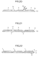
- FIG. 20 is a typical illustration showing a state in which a resin is under-fill applied between the semiconductor chips and the module substrate base material upon manufacture of the semiconductor device according to the present embodiment 1;
- FIG. 21 is a typical illustration showing a state in which ball electrodes are formed over the module substrate base material upon manufacture of the semiconductor device according to the present embodiment 1;
- FIG. 22 is a typical illustration depicting a state in which the module substrate base material is divided to form each individual semiconductor devices upon manufacture of the semiconductor device according to the present embodiment 1;
- FIG. 23 is a typical cross-sectional view of a semiconductor device showing another embodiment (embodiment 2) of the present invention.
- FIG. 24 is a typical front view partly in section of a semiconductor device showing a further embodiment (embodiment 3) of the present invention.
- FIGS. 25 ( a )- 25 ( c ) are illustrations showing the relationship of wiring between a module substrate and a printed circuit board used for each semiconductor device illustrative of a still further embodiment (embodiment 4) of the present invention.
- FIGS. 1 through 22 are respectively views related to a semiconductor device showing one embodiment (embodiment 1) of the present invention.
- FIGS. 1 through 10 are respectively views related to the semiconductor device and respective parts which constitute the semiconductor device.
- FIGS. 11 through 14 are respectively views related to a portable telephone or portable cellular phone in which the semiconductor device according to the present embodiment 1 is incorporated.
- FIGS. 15 through 22 are respectively views related to a method of manufacturing semiconductor devices.
- FIG. 1 is a typical cross-sectional view showing a semiconductor device 1 according to the present embodiment 1 , which constitutes a high-frequency unit analog signal processing IC
- FIG. 2 is a partly enlarged cross-sectional view of the semiconductor device 1
- FIG. 3 is a perspective view of the semiconductor device 1 , respectively.
- the semiconductor device 1 has a structure wherein a semiconductor chip 3 is placed over a first main surface 2 a of a wiring board 2 by flip chip bonding and protruding bumps 4 are provided over a second main surface 2 b of the wiring board 2 .
- bumps 5 for flip chip bonding are provided over a main surface of the semiconductor chip 3 .
- the bumps 5 are formed over their corresponding electrodes 6 provided over the main surface of the semiconductor chip 3 .
- wires or interconnections 7 are provided over the first main surface 2 a of the wiring board 2 in predetermined patterns. Some of the wires 7 constitute electrode pads 8 by which the bumps 5 are fixed. Further, through holes 9 are defined in the wiring board 2 so as to intersect the wires 7 respectively. Conductors 10 are respectively formed over the surfaces of the through holes 9 by plating or the like. Parts of the second main surface 2 b with the through holes 9 defined therein serve as electrodes 11 , and the bumps 4 are provided over the electrodes 11 , respectively.
- an opening 15 which extends through the wiring board 2 , is provided in the central portion of the wiring board 2 .
- Capacitors 16 which constitute chip parts respectively, are placed over the main surface of the semiconductor chip 3 , which corresponds to a region or area lying within the opening 15 . The capacitors 16 are held within the opening 15 and does not protrude from the second main surface 2 b of the wiring board 2 .
- Respective electrode portions of the capacitors 16 are electrically connected to their corresponding bumps 5 formed over the main surface of the semiconductor chip 3 in advance.
- the bumps 5 are identical in structure to the bumps 5 electrically connected to their corresponding electrode pads 8 of the wiring board 2 and are formed simultaneously upon the formation of the semiconductor chip 3 .
- FIG. 6 is a view showing the main surface of the semiconductor chip 3 .
- the bumps 5 provided along the periphery of the semiconductor chip 3 are respectively fixed to the electrode pads 8 of the wiring board 2 . Further, the bumps 5 , which exist in the central portion of the semiconductor chip 3 , place the capacitors 16 thereon (see FIG. 2 ). The electrode portions of the capacitors 16 are fixed to the bumps 5 respectively.
- FIG. 7 is a view showing the main surface of the semiconductor chip 3 which indicates a state in which the capacitors 16 are placed thereon. The five capacitors 16 are placed on the main surface thereof in the drawing.
- the capacitors 16 serve as power decoupling capacitors for reducing switching noise. While only one capacitor 16 is shown in FIG. 1, the five power decoupling capacitors 16 are placed as described above in the present embodiment 1.
- a resin (underfill resin) 17 is charged into a clearance or gap between the first main surface 2 a of the wiring board 2 and the main surface of the semiconductor chip 3 , thereby improving moisture resistance.
- the underfill resin 17 blocks even the peripheries of the respective capacitors 16 .
- the underfill resin 17 is formed by charging a resin even from the opening 15 side and curing it.
- the semiconductor device 1 according to the present embodiment 1 is a so-called chip size package (CSP) type.
- the wiring board 2 approximates to the semiconductor chip 3 in size and is slightly larger than the semiconductor chip 3 in dimension.
- the bumps 5 arranged on the center side of the semiconductor chip 3 are respectively power bumps.
- interconnections or wires drawn from circuit parts (operating blocks) of the high-frequency unit analog signal processing IC built in the semiconductor device 1 are drawn to the central portion of the semiconductor chip 3 as power bumps [corresponding to high-potential power supply or source wires (Vcc) and low-potential source wires (grounds)].
- the electrodes of the capacitors 16 are fixed to these respective pairs of power bumps respectively.
- the bumps 4 provided over the second main surface 2 b of the wiring board 2 comprise signal terminals 4 a comprised of bumps arranged along the periphery of the wiring board and power terminals 4 b comprised of bumps arranged along the inside of the signal terminals 4 a and along the edge of the opening 15 .
- the electrodes of the respective capacitors 16 and the power terminals 4 b arranged along the edge of the opening 15 are respectively electrically connected to one another.
- this is because when the pitch of each bump 4 is small, wires or interconnections connected to the inner power terminals 4 b cannot be drawn between the outer signal terminals 4 a in the wiring board (printed circuit board) on which the semiconductor device 1 is implemented.
- This is a structure adopted to introduce the wires coupled to the inner power terminals 4 b into the rear side of the wiring board through the through holes and draw the wires outside from the outer signal terminals 4 a on the rear side of the wiring board.
- FIG. 5 is a typical illustration showing the relation among the wiring board 2 , signal terminals 4 a and power terminals 4 b provided over the wiring board 2 , opening 15 defined in the wiring board 2 , semiconductor chip 3 , and capacitors 16 placed on the semiconductor chip 3 .
- the semiconductor device 1 according to the present embodiment 1 is implemented over a wiring board (motherboard) 20 for a portable cellular phone, for example.
- FIG. 11 is a front view showing the state of mounting of the semiconductor device 1
- FIG. 12 is a partly enlarged cross-sectional view thereof
- FIG. 13 is a typical plan view showing the correlation between bumps 4 provided over a wiring board 2 which constitutes the semiconductor device 1 in the implemented state of the semiconductor device 1 , and through holes or the like defined in the wiring board (motherboard) for the portable cellular phone.
- wires or interconnections 21 are provided over a mounting surface 20 b of the wiring board (motherboard) 20 for the portable cellular phone, on which the semiconductor device 1 is placed, and a reverse side or back 20 b of the wiring board 20 .
- Some of the wires 21 respectively form bump fixing pads 22 to which the bumps 4 of the semiconductor device 1 are fixed.
- the motherboard 20 has through holes 23 provided so as to cross the wires 21 placed over the front and back thereof.
- Conductors 24 are provided over the surfaces of the through holes 23 by plating or the like.
- the through holes 23 are provided so as to be opposed to the space area W on the second main surface 2 b of the wiring board 2 for the semiconductor device 1 .
- the inner power terminals 4 b (4) of the semiconductor device 1 are electrically connected to the wires 21 on the mounting surface 20 b of the motherboard 20 , the conductors 24 placed on the through holes 23 , and the wires 21 on the back 20 b . Therefore, the wires 21 on the back 20 b of the motherboard 20 can be extended outside from the outer signal terminals 4 a (4) to draw the wires outside from the row of the outer signal terminals 4 a . Thus, this can cope with the case where the pitch of each signal terminal 4 a is narrow and the wires cannot be formed so as to pass between the signal terminals 4 a .
- b a bump pitch
- the space area W results in 0.7 mm.
- the wires drawn outside from the outer signal terminals 4 a may be drawn to the mounting surface 20 b of the motherboard 20 again owing to the provision of through holes. This can freely be selected according to wiring design.
- a functional configuration of the digital cellular type portable telephone in which the semiconductor device 1 according to the present embodiment 1 is built, will now be described with reference to FIG. 14 .
- a transmission system from a baseband unit 50 to an antenna switch 60 comprises, for example, a quadrature modulator 51 with a signal (I, Q) sent from the baseband unit 50 being set as an input signal, a phase comparator 52 , a voltage-controlled oscillator (VCO) 53 , and a power amplifier (PA) 54 .
- a quadrature modulator 51 with a signal (I, Q) sent from the baseband unit 50 being set as an input signal a phase comparator 52 , a voltage-controlled oscillator (VCO) 53 , and a power amplifier (PA) 54 .
- VCO voltage-controlled oscillator
- PA power amplifier
- a reception system from the antenna switch 60 to the baseband unit 50 comprises, for example, a low noise amplifier (LNA) 61 , a first mixer 62 , a second mixer 63 , an automatic gain controller (AGC) 64 , and a quadrature modulator 65 for outputting a signal (I,Q) to the baseband unit 50 .
- LNA low noise amplifier
- AGC automatic gain controller
- quadrature modulator 65 for outputting a signal (I,Q) to the baseband unit 50 .
- a RFVCO 74 is controlled by a first synthesizer (PLL 1 ) 72 of a dual synthesizer (offset synthesizer) 71 which inputs or receives a signal having a frequency defined as the reference from a temperature compensating crystal oscillator (TCXO) 70 .
- a signal outputted from the RFVCO 74 is inputted to the first mixer 62 .
- a signal outputted from the first synthesizer (PLL 1 ) 72 is inputted to a third mixer 75 .
- a signal outputted from the voltage-controlled oscillator (VCO) 53 is also inputted to the third mixer 75 .
- a signal outputted from the third mixer 75 is inputted to the phase comparator 52 .
- An IFVCO 76 is controlled by a second synthesizer (PLL 2 ) 73 of the dual synthesizer 71 .
- a signal outputted from the IFVCO 76 is outputted to a frequency divider 77 .
- the frequency divider 77 inputs signals to the quadrature modulator 51 of the transmission system and the quadrature modulator 65 and second mixer 63 of the reception system respectively.
- a speaker 91 , a microphone 92 , and a key control unit 93 , etc. are connected to the baseband unit 50 .
- an antenna 80 is connected to the antenna switch 60 .
- a signal received by the antenna 80 is inputted to the low noise amplifier (LNA) 61 through the antenna switch 60 .
- the signal amplified by the low noise amplifier 61 is frequency-converted into an intermediate frequency by the first mixer 62 based on the signal outputted from the RFVCO 74 .
- the signal outputted from the first mixer 62 is frequency-converted by the second mixer 63 again based on the signal outputted from the frequency divider 77 .
- the RFVCO 74 and the IFVCO 76 for sending the output signal to the frequency divider 77 are controlled by the first synthesizer (PLL 1 ) 72 and the second synthesizer (PLL 2 ) 73 respectively.
- the output signal of the second mixer 63 is gain-controlled by the automatic gain controller (AGC) 64 and demodulated by the quadrature modulator 65 in response to the output signal of the frequency divider 77 , whereby an I/Q signal is obtained.
- the I/Q signal is outputted to the baseband unit 50 and radiated from the speaker 91 as a sound signal.
- the sound signal inputted from the microphone 92 is changed to an I/Q signal by the baseband unit 50 and outputted to the quadrature modulator 51 .
- the quadrature modulator 51 modulates the I/Q signal, based on the output signal of the frequency divider 77 .
- the phase comparator 52 compares the phase of a signal outputted from the quadrature modulator 51 and that of a signal outputted from the third mixer 75 and outputs a signal for controlling the VCO 53 according to the difference in phase therebetween.
- a signal outputted from the VCO 53 is sent to the third mixer 75 as well as to the power amplifier 54 , where it is frequency-converted into an intermediate frequency to be compared in phase by the phase comparator 52 .
- the output signal of the VCO 53 is modulated based on the I/Q signal of the baseband unit 50 , whereby a transmitting signal is obtained.
- the power amplifier 54 amplifies the output of the VCO 53 .
- the output signal of the power amplifier 54 is radiated from the antenna 80 as radio waves by performing switching to the antenna switch 60 .
- a portion given by a frame indicated by a two-dot chain line in FIG. 14, i.e., the quadrature modulator 51 , phase comparator 52 , offset synthesizer 71 , first mixer 62 , second mixer 63 , third mixer 75 , automatic gain controller (AGC) 64 , quadrature modulator 65 and frequency divider 77 are monolithically formed over the semiconductor chip 3 .
- a bias circuit 78 for controlling the low noise amplifier (LNA) 61 is also monolithically built in the semiconductor chip 3 .
- FIG. 8 is a typical illustration showing respective functional blocks for the semiconductor chip 3 .
- Square portions arranged along the periphery of the semiconductor chip 3 correspond to bumps 5 respectively.
- the low noise amplifier (LNA) 61 can also be incorporated monolithically into the semiconductor chip 3 .
- capacitors 16 are incorporated into the functional blocks as follows.
- a capacitor CD 1 is built in the first mixer 62
- a capacitor C D 2 is built in the second mixer 63 and the automatic gain controller (AGC) 64
- a capacitor C D 3 is built in the quadrature modulators 51 and 65 of the transmission and reception systems
- a capacitor C D 4 is built in the offset synthesizer 71
- a capacitor C D 5 is built in the frequency divider 77 , respectively.
- the bumps 5 provided over the main surface of the semiconductor chip 3 take such an arrangement as shown in FIG. 6 as described above.
- the ten bumps 5 corresponding to the sum of five pairs ⁇ two bumps are provided in the central portion of the main surface of the semiconductor chip 3 to place the five capacitors 16 in the central portion thereof. Further, the forty-eight bumps 5 are placed side by side along the periphery of the semiconductor chip 3 .
- the capacitors 16 are incorporated into a ground wiring unit and a power wiring unit and serve as power decoupling capacitors for reducing switching noise.
- the state of placement of the capacitors 16 is shown in FIGS. 4 and 7.
- FIG. 4 shows the relationship between the capacitor C D 2 and the bumps 4 (corresponding to the signal terminals 4 a and the power terminals 4 b ) provided over the second main surface 2 b of the wiring board 2 in particular.
- the power terminals 4 b indicate G 4 through G 7 respectively
- the signal terminals 4 a indicate J 5 through J 9 respectively.
- An arrangement of these terminals corresponds to the arrangement of the bumps 5 , which is shown at a lower-right portion of FIG. 8 in the case of the semiconductor chip 3 .
- Capacitors C d 1 through C D 5 are shown even in FIG. 8 .
- the positions of these capacitors C D 1 through C D 5 are those shown for convenience to understand the relation between their positions and the circuit respective parts.
- wires connected to Vcc and GND of the bumps 5 placed along the peripheral edge of the semiconductor chip 3 are drawn to the center side of the semiconductor chip 3 . Further, the leading ends of the wires serve as the bumps 5 connected to their corresponding electrodes of the capacitors.
- the respective capacitors C D 1 through C D5 are placed on their corresponding center positions of the semiconductor chip 3 as shown in FIGS. 4 and 7.
- the semiconductor device 1 according to the present embodiment 1 is manufactured through respective process steps comprising a work start [Step (S) 101 ], bump formation [S 102 ], dicing [S 103 ], capacitor loading [S 104 ], flip chip bonding [S 105 ], underfill resin application [S 106 ], bump formation [S 107 ], wiring board division [S 108 ], and work end [S 109 ] as indicated by a flowchart of FIG. 15 .
- a dicing device is next used to dice the semiconductor substrate 30 and thereby divide it, whereby a plurality of semiconductor chips 3 are formed as shown in FIG. 17 .
- power decoupling capacitors 16 are placed over each semiconductor chip 3 .
- the five capacitors 16 are placed over the semiconductor chip 3 as shown in FIG. 7 .
- each of the semiconductor chips 3 is absorbed and held under vacuum at a lower end of a vacuum absorption tool (collet) 31 so that the bumps 5 are turned upside down.
- the semiconductor chips 3 are placed over a wiring board base material 32 one by one by flip chip bonding.
- Wiring blocks having predetermined wiring patterns formed vertically and horizontally are formed in line over the wiring board base material 32 .
- These wiring blocks are thereafter cut to form the wiring boards 2 shown in FIGS. 9 and 10.
- the opening 15 is defined in the central portion of each wiring block.
- a resin liquid (underfill resin liquid) 33 is charged into clearances or gaps defined between the wiring board base material 32 and the semiconductor chips 3 by an injector 34 .
- the wiring board base material 32 is turned upside down and the underfill resin liquid may be applied to the main surface side of each semiconductor chip 3 through the opening 15 to charge a resin into the gap between the wiring board base material 32 and each semiconductor chip 3 .
- the resin comprises an epoxy resin, for example and is cured by a heat curing process.
- resins (underfill resins) 17 for blocking between the semiconductor chips 3 and the wiring board base material 32 are formed as shown in FIG. 21 .
- bumps 4 are formed over the back of the wiring board base material 32 as shown in FIG. 21.
- a method of forming the bumps is considered in various forms. In the present embodiment 1, however, bump materials are printed to predetermined thicknesses by screen printing or the like and thereafter subjected to heat treatment (reflow processing) to thereby form ball-shaped bumps 4 through the use of surface tensions of the bump materials.
- An arrangement of the bumps 4 is represented as shown in FIG. 10 .
- the wiring board base material 32 is divided vertically and horizontally to form a plurality of semiconductor devices 1 as shown in FIG. 22 .
- a portable cellular phone with the semiconductor device 1 built therein which provides less switching noise, can be provided because it can achieve a reduction in switching noise.
- the state of a call thereof becomes always satisfactory.
- a wiring board (motherboard) 20 with the semiconductor device 1 implemented thereon takes a structure wherein through holes 23 having conductors 24 formed over their surfaces are formed at portions each corresponding to the space area W, and wires or interconnections drawn from the inner row of bumps 4 are drawn to a reverse side or back 20 b of the motherboard 20 through the use of the through holes 23 to thereby form drawn wires over the back of the motherboard 20 .
- the pitch of each of the bumps lying in each bump row can be reduced.
- the semiconductor chip and the wiring board can be brought into less size, and the numbers of obtainable semiconductor chips and wiring boards formed of one semiconductor substrate and one wiring board base material increase, whereby the manufacturing cost of each semiconductor device can be reduced.
- the wiring board (motherboard) with the semiconductor device implemented thereon is also reduced in size and hence a reduction in the cost of an electronic device can also be achieved.
- FIG. 23 is a typical cross-sectional view of a semiconductor device showing another embodiment (embodiment 2) of the present invention.
- a semiconductor device 1 according to the present embodiment 2 has a structure wherein a recess 40 is defined in a first main surface 2 a of a wiring board 2 in the structure employed in the embodiment 1.
- the recess 40 is provided in place of the opening 15 .
- Five capacitors 16 placed over a main surface of a semiconductor chip 3 are located in this recess.
- a resin (underfill resin) 17 to be charged between the semiconductor chip 3 and the wiring board 2 is also charged into the recess 40 .
- the semiconductor device 1 according to the present embodiment 2 can also achieve a reduction in switching noise in a manner similar to the embodiment 1.
- FIG. 24 is a typical front view partly in section of a semiconductor device showing a further embodiment (embodiment 3) of the present invention.
- a semiconductor device 1 according to the present embodiment 3 has a structure wherein without providing the opening and recess as in the embodiments referred to above, capacitors 16 are placed over a main surface of a semiconductor chip 3 , a surface on which the capacitors 16 are placed, is opposed to a first main surface 2 a of a wiring board 2 , and the semiconductor chip 3 is implemented over the wiring board 2 with bumps 5 provided over the semiconductor chip 3 interposed therebetween.
- the present structure needs to lengthen each bump 5 provided over the semiconductor chip 3 along the direction of its thickness, for example.
- the semiconductor device 1 takes a structure wherein the power decoupling capacitors 16 are directly placed over the main surface of the semiconductor chip 3 in terms of the characteristics of the semiconductor device 1 , the present embodiment can reduce switching noise in a similar to the respective embodiments referred to above.
- FIGS. 25 ( a ) through 25 ( c ) are respectively typical illustrations showing the relationships of wiring between module substrates and printed circuit boards used for respective semiconductor devices each illustrative of a still further embodiment (embodiment 4) of the present invention.
- FIG. 25 ( a ) shows an example in which forty-eight bumps 4 are provided over a second main surface of a wiring board 2
- FIG. 25 ( b ) illustrates an example in which sixty-four bumps 4 are provided over a second main surface of a wiring board 2
- FIG. 25 ( c ) depicts an example in which eighty-four bumps 4 are provided over a second surface of a wiring board 2 , respectively. These bumps 4 are indicated by white circles respectively.
- FIGS. 25 ( a ) and 25 ( b ) are respectively examples in which bump rows are rectangularly arranged in double form
- FIG. 25 ( c ) is an example in which bump rows are rectangularly arranged in triple form.
- parts indicated by black circles respectively correspond through holes 23 defined in wiring boards (motherboards) 20 on which the semiconductor devices are implemented, and conductors 24 formed over the surfaces of the through holes 23 .
- Lines for connecting the black circles and the white circles, and lines extending outside the outermost white circles are respectively wires or interconnections 21 provided over mounting surfaces on which the semiconductor devices of the wiring boards (motherboards) 20 are placed.
- each wiring board 2 when the bump rows provided over the second main surface of each wiring board 2 are arranged as a multiple row, a space area, which allows one or more rows of terminals (through holes) to be provided between the respective rows, is provided to thereby eliminate for the need of drawing wires drawn from the inner row of bumps 4 between the bumps on the outer side. It is therefore possible to reduce the pitch of each of the bumps lying in each bump row. As a result, the semiconductor chips and the wiring boards can be brought into less size, and the numbers of obtainable semiconductor chips and wiring boards formed of one semiconductor substrate and one wiring board base material increase, whereby the manufacturing cost of each semiconductor device can be reduced. Further, the wiring board (motherboad) with the semiconductor device implemented thereon is also reduced in size and hence a reduction in the cost of an electronic device can also be achieved.
- An interval between bump rows provided in double form over a wiring substrate surface of a semiconductor device serves as a space area W which allows the provision of one or more rows of terminals (through holes).
- a wiring board (motherboard) with the semiconductor device implemented thereon takes a structure wherein through holes having conductors formed over their surfaces are formed at portions each corresponding to the space area W of the wiring board (motherboard), and wires or interconnections drawn from the inner row of bumps are drawn to a reverse side or back of the motherboard through the use of the through holes.
- the semiconductor chip and the wiring board can be brought into less size, and the numbers of obtainable semiconductor chips and wiring boards formed of one semiconductor substrate and one wiring board base material increase, whereby the manufacturing cost of each semiconductor device can be reduced. Further, the motherboard with the semiconductor device implemented thereon is also reduced in size and hence a reduction in the cost of an electronic device can also be achieved.
- a semiconductor device in which power decoupling capacitors comprising chip capacitors are built to reduce switching noise, is suitable as a semiconductor device for a radio communication device, such as a portable cellular phone or the like.
Abstract
Description
Claims (14)
Applications Claiming Priority (3)
| Application Number | Priority Date | Filing Date | Title |
|---|---|---|---|
| JP17057099 | 1999-06-17 | ||
| JP11-170570 | 1999-06-17 | ||
| PCT/JP2000/003907 WO2000079592A1 (en) | 1999-06-17 | 2000-06-15 | Semiconductor device and electronic device |
Publications (1)
| Publication Number | Publication Date |
|---|---|
| US6335566B1 true US6335566B1 (en) | 2002-01-01 |
Family
ID=15907296
Family Applications (1)
| Application Number | Title | Priority Date | Filing Date |
|---|---|---|---|
| US09/646,712 Expired - Lifetime US6335566B1 (en) | 1999-06-17 | 2000-06-15 | Semiconductor device and an electronic device |
Country Status (2)
| Country | Link |
|---|---|
| US (1) | US6335566B1 (en) |
| WO (1) | WO2000079592A1 (en) |
Cited By (28)
| Publication number | Priority date | Publication date | Assignee | Title |
|---|---|---|---|---|
| US20020060904A1 (en) * | 2000-09-26 | 2002-05-23 | Kazuhito Higuchi | Electronic component, circuit device, method for manufacturing the circuit device, and semiconductor device |
| US20020127771A1 (en) * | 2001-03-12 | 2002-09-12 | Salman Akram | Multiple die package |
| US20030006496A1 (en) * | 2001-03-15 | 2003-01-09 | Venkateshwaran Vaiyapuri | Semiconductor/printed circuit board assembly, and computer system |
| US20030085024A1 (en) * | 2001-09-28 | 2003-05-08 | Santiago Juan G | Control of electrolysis gases in electroosmotic pump systems |
| US6606251B1 (en) | 2002-02-07 | 2003-08-12 | Cooligy Inc. | Power conditioning module |
| US20030151905A1 (en) * | 2002-02-11 | 2003-08-14 | Adc Dsl Systems, Inc. | Electrical connections within substrates |
| US20030184963A1 (en) * | 2002-04-01 | 2003-10-02 | Eskildsen Steven R. | Providing in package power supplies for integrated circuits |
| US20030222356A1 (en) * | 2002-05-31 | 2003-12-04 | Nec Corporation | Semiconductor integrated circuit, printed circuit board and electronic apparatus |
| US20040036169A1 (en) * | 2002-08-23 | 2004-02-26 | Shinko Electric Industries Co., Ltd. | Semiconductor package and semiconductor device |
| US20040089442A1 (en) * | 2001-09-28 | 2004-05-13 | The Board Of Trustees Of The Leland Stanford Junior University | Electroosmotic microchannel cooling system |
| US6744131B1 (en) * | 2003-04-22 | 2004-06-01 | Xilinx, Inc. | Flip chip integrated circuit packages accommodating exposed chip capacitors while providing structural rigidity |
| US20040188834A1 (en) * | 2003-03-26 | 2004-09-30 | Satoru Konishi | Semiconductor device |
| US6812566B2 (en) * | 2002-01-02 | 2004-11-02 | Intel Corporation | Lower profile package with power supply in package |
| US20040229403A1 (en) * | 2001-03-30 | 2004-11-18 | Salman Akram | Die stacking scheme |
| US20050200007A1 (en) * | 2004-03-11 | 2005-09-15 | Advanced Semiconductor Engineering, Inc. | Semiconductor package |
| US20050201175A1 (en) * | 2004-02-05 | 2005-09-15 | Josef Fenk | Radio frequency arrangement, method for producing a radio frequency arrangement and use of the radio frequency arrangement |
| EP1711963A2 (en) * | 2003-12-22 | 2006-10-18 | Intel Corporation | Integrating passive components on spacer in stacked dies |
| US7217597B2 (en) | 2004-06-22 | 2007-05-15 | Micron Technology, Inc. | Die stacking scheme |
| US20070136766A1 (en) * | 2005-12-09 | 2007-06-14 | Ryuichi Iwamura | Cross-phase adapter for powerline communications (PLC) network |
| US20090174060A1 (en) * | 2001-02-06 | 2009-07-09 | Renesas Technology Corp. | Hybrid integrated circuit device, and method for fabricating the same, and electronic device |
| US20100127370A1 (en) * | 2008-11-25 | 2010-05-27 | Shinko Electric Industries Co., Ltd. | Wiring board, semiconductor device and semiconductor element |
| US20100149773A1 (en) * | 2008-12-17 | 2010-06-17 | Mohd Hanafi Mohd Said | Integrated circuit packages having shared die-to-die contacts and methods to manufacture the same |
| US20100164084A1 (en) * | 2008-12-26 | 2010-07-01 | Jun-Ho Lee | Semiconductor device and semiconductor package including the same |
| US20140008798A1 (en) * | 2011-03-22 | 2014-01-09 | Shinji Baba | Semiconductor device |
| US20150041955A1 (en) * | 2013-08-09 | 2015-02-12 | Apple Inc. | Multi-Die Fine Grain Integrated Voltage Regulation |
| US9466545B1 (en) * | 2007-02-21 | 2016-10-11 | Amkor Technology, Inc. | Semiconductor package in package |
| US10468381B2 (en) | 2014-09-29 | 2019-11-05 | Apple Inc. | Wafer level integration of passive devices |
| US11404365B2 (en) | 2019-05-07 | 2022-08-02 | International Business Machines Corporation | Direct attachment of capacitors to flip chip dies |
Citations (11)
| Publication number | Priority date | Publication date | Assignee | Title |
|---|---|---|---|---|
| JPH06302714A (en) | 1993-04-13 | 1994-10-28 | Matsushita Electric Ind Co Ltd | Semiconductor device |
| US5608262A (en) * | 1995-02-24 | 1997-03-04 | Lucent Technologies Inc. | Packaging multi-chip modules without wire-bond interconnection |
| US5635767A (en) | 1995-06-02 | 1997-06-03 | Motorola, Inc. | Semiconductor device having built-in high frequency bypass capacitor |
| US5646828A (en) * | 1995-02-24 | 1997-07-08 | Lucent Technologies Inc. | Thin packaging of multi-chip modules with enhanced thermal/power management |
| JPH09260537A (en) | 1996-03-26 | 1997-10-03 | Sumitomo Kinzoku Electro Device:Kk | Flip chip ceramic substrate |
| US5808878A (en) * | 1995-03-16 | 1998-09-15 | Kabushiki Kaisha Toshiba | Circuit substrate shielding device |
| US5869894A (en) * | 1997-07-18 | 1999-02-09 | Lucent Technologies Inc. | RF IC package |
| US6150724A (en) * | 1998-03-02 | 2000-11-21 | Motorola, Inc. | Multi-chip semiconductor device and method for making the device by using multiple flip chip interfaces |
| US6181008B1 (en) * | 1998-11-12 | 2001-01-30 | Sarnoff Corporation | Integrated circuit power supply |
| US6201302B1 (en) * | 1998-12-31 | 2001-03-13 | Sampo Semiconductor Corporation | Semiconductor package having multi-dies |
| US6204562B1 (en) * | 1999-02-11 | 2001-03-20 | United Microelectronics Corp. | Wafer-level chip scale package |
-
2000
- 2000-06-15 US US09/646,712 patent/US6335566B1/en not_active Expired - Lifetime
- 2000-06-15 WO PCT/JP2000/003907 patent/WO2000079592A1/en active Application Filing
Patent Citations (11)
| Publication number | Priority date | Publication date | Assignee | Title |
|---|---|---|---|---|
| JPH06302714A (en) | 1993-04-13 | 1994-10-28 | Matsushita Electric Ind Co Ltd | Semiconductor device |
| US5608262A (en) * | 1995-02-24 | 1997-03-04 | Lucent Technologies Inc. | Packaging multi-chip modules without wire-bond interconnection |
| US5646828A (en) * | 1995-02-24 | 1997-07-08 | Lucent Technologies Inc. | Thin packaging of multi-chip modules with enhanced thermal/power management |
| US5808878A (en) * | 1995-03-16 | 1998-09-15 | Kabushiki Kaisha Toshiba | Circuit substrate shielding device |
| US5635767A (en) | 1995-06-02 | 1997-06-03 | Motorola, Inc. | Semiconductor device having built-in high frequency bypass capacitor |
| JPH09260537A (en) | 1996-03-26 | 1997-10-03 | Sumitomo Kinzoku Electro Device:Kk | Flip chip ceramic substrate |
| US5869894A (en) * | 1997-07-18 | 1999-02-09 | Lucent Technologies Inc. | RF IC package |
| US6150724A (en) * | 1998-03-02 | 2000-11-21 | Motorola, Inc. | Multi-chip semiconductor device and method for making the device by using multiple flip chip interfaces |
| US6181008B1 (en) * | 1998-11-12 | 2001-01-30 | Sarnoff Corporation | Integrated circuit power supply |
| US6201302B1 (en) * | 1998-12-31 | 2001-03-13 | Sampo Semiconductor Corporation | Semiconductor package having multi-dies |
| US6204562B1 (en) * | 1999-02-11 | 2001-03-20 | United Microelectronics Corp. | Wafer-level chip scale package |
Cited By (60)
| Publication number | Priority date | Publication date | Assignee | Title |
|---|---|---|---|---|
| US6862189B2 (en) * | 2000-09-26 | 2005-03-01 | Kabushiki Kaisha Toshiba | Electronic component, circuit device, method for manufacturing the circuit device, and semiconductor device |
| US20020060904A1 (en) * | 2000-09-26 | 2002-05-23 | Kazuhito Higuchi | Electronic component, circuit device, method for manufacturing the circuit device, and semiconductor device |
| US7755182B2 (en) * | 2001-02-06 | 2010-07-13 | Renesas Technology Corp. | Hybrid integrated circuit device, and method for fabricating the same, and electronic device |
| US20090174060A1 (en) * | 2001-02-06 | 2009-07-09 | Renesas Technology Corp. | Hybrid integrated circuit device, and method for fabricating the same, and electronic device |
| US20020127771A1 (en) * | 2001-03-12 | 2002-09-12 | Salman Akram | Multiple die package |
| US20050189623A1 (en) * | 2001-03-12 | 2005-09-01 | Salman Akram | Multiple die package |
| US20040173889A1 (en) * | 2001-03-12 | 2004-09-09 | Salman Akram | Multiple die package |
| US7427535B2 (en) | 2001-03-15 | 2008-09-23 | Micron Technology, Inc. | Semiconductor/printed circuit board assembly, and computer system |
| US20030006496A1 (en) * | 2001-03-15 | 2003-01-09 | Venkateshwaran Vaiyapuri | Semiconductor/printed circuit board assembly, and computer system |
| US7514776B2 (en) | 2001-03-15 | 2009-04-07 | Micron Technology, Inc. | Semiconductor/printed circuit board assembly, and computer system |
| US20050106780A1 (en) * | 2001-03-15 | 2005-05-19 | Venkateshwaran Vaiyapuri | Semiconductor/printed circuit board assembly, and computer system |
| US6869827B2 (en) | 2001-03-15 | 2005-03-22 | Micron Technology, Inc. | Semiconductor/printed circuit board assembly, and computer system |
| US20070120238A1 (en) * | 2001-03-15 | 2007-05-31 | Micron Technology, Inc. | Semiconductor/printed circuit board assembly, and computer system |
| US20040229403A1 (en) * | 2001-03-30 | 2004-11-18 | Salman Akram | Die stacking scheme |
| US7008823B2 (en) | 2001-03-30 | 2006-03-07 | Micron Technology, Inc. | Die stacking scheme |
| US7112878B2 (en) | 2001-03-30 | 2006-09-26 | Micron Technology, Inc. | Die stacking scheme |
| US20040245627A1 (en) * | 2001-03-30 | 2004-12-09 | Salman Akram | Die stacking scheme |
| US20030085024A1 (en) * | 2001-09-28 | 2003-05-08 | Santiago Juan G | Control of electrolysis gases in electroosmotic pump systems |
| US20050205241A1 (en) * | 2001-09-28 | 2005-09-22 | The Board Of Trustees Of The Leland Stanford Junior University | Closed-loop microchannel cooling system |
| US20040089442A1 (en) * | 2001-09-28 | 2004-05-13 | The Board Of Trustees Of The Leland Stanford Junior University | Electroosmotic microchannel cooling system |
| US6812566B2 (en) * | 2002-01-02 | 2004-11-02 | Intel Corporation | Lower profile package with power supply in package |
| US6606251B1 (en) | 2002-02-07 | 2003-08-12 | Cooligy Inc. | Power conditioning module |
| US6678168B2 (en) | 2002-02-07 | 2004-01-13 | Cooligy, Inc. | System including power conditioning modules |
| US7152312B2 (en) | 2002-02-11 | 2006-12-26 | Adc Dsl Systems, Inc. | Method for transmitting current through a substrate |
| US20030151905A1 (en) * | 2002-02-11 | 2003-08-14 | Adc Dsl Systems, Inc. | Electrical connections within substrates |
| US7823279B2 (en) | 2002-04-01 | 2010-11-02 | Intel Corporation | Method for using an in package power supply to supply power to an integrated circuit and to a component |
| WO2003085725A2 (en) * | 2002-04-01 | 2003-10-16 | Intel Corporation | In package power supplies for integrated circuits |
| WO2003085725A3 (en) * | 2002-04-01 | 2004-09-10 | Intel Corp | In package power supplies for integrated circuits |
| US20030184963A1 (en) * | 2002-04-01 | 2003-10-02 | Eskildsen Steven R. | Providing in package power supplies for integrated circuits |
| US6924562B2 (en) * | 2002-05-31 | 2005-08-02 | Nec Corporation | Semiconductor integrated circuit having at least one of a power supply plane and ground plane divided into parts insulated from one another |
| US20030222356A1 (en) * | 2002-05-31 | 2003-12-04 | Nec Corporation | Semiconductor integrated circuit, printed circuit board and electronic apparatus |
| US6833614B2 (en) * | 2002-08-23 | 2004-12-21 | Shinko Electric Industries Co., Ltd. | Semiconductor package and semiconductor device |
| US20040036169A1 (en) * | 2002-08-23 | 2004-02-26 | Shinko Electric Industries Co., Ltd. | Semiconductor package and semiconductor device |
| US20060267220A1 (en) * | 2003-03-26 | 2006-11-30 | Satoru Konishi | Semiconductor device |
| US20040188834A1 (en) * | 2003-03-26 | 2004-09-30 | Satoru Konishi | Semiconductor device |
| US6744131B1 (en) * | 2003-04-22 | 2004-06-01 | Xilinx, Inc. | Flip chip integrated circuit packages accommodating exposed chip capacitors while providing structural rigidity |
| EP1711963A2 (en) * | 2003-12-22 | 2006-10-18 | Intel Corporation | Integrating passive components on spacer in stacked dies |
| US7495276B2 (en) * | 2004-02-05 | 2009-02-24 | Infineon Technologies Ag | Radio frequency arrangement, method for producing a radio frequency arrangement and use of the radio frequency arrangement |
| US20050201175A1 (en) * | 2004-02-05 | 2005-09-15 | Josef Fenk | Radio frequency arrangement, method for producing a radio frequency arrangement and use of the radio frequency arrangement |
| US7091607B2 (en) * | 2004-03-11 | 2006-08-15 | Advanced Semiconductor Engineering Inc. | Semiconductor package |
| US20050200007A1 (en) * | 2004-03-11 | 2005-09-15 | Advanced Semiconductor Engineering, Inc. | Semiconductor package |
| US7217597B2 (en) | 2004-06-22 | 2007-05-15 | Micron Technology, Inc. | Die stacking scheme |
| US20070136766A1 (en) * | 2005-12-09 | 2007-06-14 | Ryuichi Iwamura | Cross-phase adapter for powerline communications (PLC) network |
| US9768124B2 (en) | 2007-02-21 | 2017-09-19 | Amkor Technology, Inc. | Semiconductor package in package |
| US9466545B1 (en) * | 2007-02-21 | 2016-10-11 | Amkor Technology, Inc. | Semiconductor package in package |
| US20100127370A1 (en) * | 2008-11-25 | 2010-05-27 | Shinko Electric Industries Co., Ltd. | Wiring board, semiconductor device and semiconductor element |
| US7884463B2 (en) * | 2008-11-25 | 2011-02-08 | Shinko Electric Industries Co., Ltd. | Wiring board, semiconductor device and semiconductor element |
| US20100149773A1 (en) * | 2008-12-17 | 2010-06-17 | Mohd Hanafi Mohd Said | Integrated circuit packages having shared die-to-die contacts and methods to manufacture the same |
| US8035194B2 (en) * | 2008-12-26 | 2011-10-11 | Hynix Semiconductor Inc. | Semiconductor device and semiconductor package including the same |
| US20100164084A1 (en) * | 2008-12-26 | 2010-07-01 | Jun-Ho Lee | Semiconductor device and semiconductor package including the same |
| US20140008798A1 (en) * | 2011-03-22 | 2014-01-09 | Shinji Baba | Semiconductor device |
| US9293405B2 (en) * | 2011-03-22 | 2016-03-22 | Renesas Electronics Corporation | Semiconductor device |
| US20150041955A1 (en) * | 2013-08-09 | 2015-02-12 | Apple Inc. | Multi-Die Fine Grain Integrated Voltage Regulation |
| US9595526B2 (en) * | 2013-08-09 | 2017-03-14 | Apple Inc. | Multi-die fine grain integrated voltage regulation |
| US10056384B2 (en) | 2013-08-09 | 2018-08-21 | Apple Inc. | Multi-die fine grain integrated voltage regulation |
| US10411012B2 (en) | 2013-08-09 | 2019-09-10 | Apple Inc. | Multi-die fine grain integrated voltage regulation |
| US11063046B2 (en) | 2013-08-09 | 2021-07-13 | Apple Inc. | Multi-die fine grain integrated voltage regulation |
| US10468381B2 (en) | 2014-09-29 | 2019-11-05 | Apple Inc. | Wafer level integration of passive devices |
| US11398456B2 (en) | 2014-09-29 | 2022-07-26 | Apple Inc. | Wafer level integration of passive devices |
| US11404365B2 (en) | 2019-05-07 | 2022-08-02 | International Business Machines Corporation | Direct attachment of capacitors to flip chip dies |
Also Published As
| Publication number | Publication date |
|---|---|
| WO2000079592A1 (en) | 2000-12-28 |
Similar Documents
| Publication | Publication Date | Title |
|---|---|---|
| US6335566B1 (en) | Semiconductor device and an electronic device | |
| US7919858B2 (en) | Semiconductor device having lands disposed inward and outward of an area of a wiring board where electrodes are disposed | |
| KR100993277B1 (en) | Semiconductor device and electronic device | |
| US7982301B2 (en) | Semiconductor device | |
| US8824994B2 (en) | Wireless communication system | |
| KR100744979B1 (en) | Sip type package containing analog semiconductor chip and digital semiconductor chip stacked in order, and method for manufacturing the same | |
| US20030060172A1 (en) | Radio frequency module | |
| JP2003060523A (en) | Radio communication module | |
| KR100993579B1 (en) | Semiconductor device and electronic device | |
| JP4137059B2 (en) | Electronic device and semiconductor device | |
| US7763960B2 (en) | Semiconductor device, method for manufacturing semiconductor device, and electric equipment system | |
| JP2000134095A (en) | Pll module and portable terminal device | |
| JP2003101320A (en) | Semiconductor integrated circuit | |
| US20050045987A1 (en) | Integrated circuit package having inductance loop formed from same-pin-to-same-bonding-pad structure | |
| JP2002313980A (en) | Semiconductor device | |
| WO2005022599A2 (en) | Integrated circuit package having inductance loop formed from same-pin-to-same-bonding-pad structure | |
| JP2004281844A (en) | Semiconductor device, semiconductor device manufacturing method, and radio communication apparatus | |
| JP2002261643A (en) | Radio communication module | |
| JP2000232326A (en) | High frequency power amplifying device and radio communication equipment | |
| WO2003094236A1 (en) | Semiconductor device and radio communication apparatus | |
| JP2001044367A (en) | Ic chip and high frequency component | |
| WO2002015272A1 (en) | Tuner device |
Legal Events
| Date | Code | Title | Description |
|---|---|---|---|
| AS | Assignment |
Owner name: HITACHI, LTD., JAPAN Free format text: ASSIGNMENT OF ASSIGNORS INTEREST;ASSIGNORS:HIRASHIMA, TOSHINORI;ENDO, TAKEFUMI;WATANABE, KAZUO;AND OTHERS;REEL/FRAME:011338/0764;SIGNING DATES FROM 20001013 TO 20001017 Owner name: HITACHI ULSI SYSTEMS CO., LTD., JAPAN Free format text: ASSIGNMENT OF ASSIGNORS INTEREST;ASSIGNORS:HIRASHIMA, TOSHINORI;ENDO, TAKEFUMI;WATANABE, KAZUO;AND OTHERS;REEL/FRAME:011338/0764;SIGNING DATES FROM 20001013 TO 20001017 Owner name: HITACHI TOHBU SEMICONDUCTOR, LTD., JAPAN Free format text: ASSIGNMENT OF ASSIGNORS INTEREST;ASSIGNORS:HIRASHIMA, TOSHINORI;ENDO, TAKEFUMI;WATANABE, KAZUO;AND OTHERS;REEL/FRAME:011338/0764;SIGNING DATES FROM 20001013 TO 20001017 |
|
| STCF | Information on status: patent grant |
Free format text: PATENTED CASE |
|
| FPAY | Fee payment |
Year of fee payment: 4 |
|
| FEPP | Fee payment procedure |
Free format text: PAYOR NUMBER ASSIGNED (ORIGINAL EVENT CODE: ASPN); ENTITY STATUS OF PATENT OWNER: LARGE ENTITY |
|
| FPAY | Fee payment |
Year of fee payment: 8 |
|
| AS | Assignment |
Owner name: RENESAS ELECTRONICS CORPORATION, JAPAN Free format text: ASSIGNMENT OF ASSIGNORS INTEREST;ASSIGNOR:HITACHI, LTD.;REEL/FRAME:026109/0976 Effective date: 20110307 |
|
| FPAY | Fee payment |
Year of fee payment: 12 |
|
| AS | Assignment |
Owner name: RENESAS ELECTRONICS CORPORATION, JAPAN Free format text: ASSIGNMENT OF ASSIGNORS INTEREST;ASSIGNOR:HITACHI ULSI SYSTEMS CO., LTD.;REEL/FRAME:032859/0252 Effective date: 20140326 |
|
| AS | Assignment |
Owner name: RENESAS NORTHERN JAPAN SEMICONDUCTOR, INC., JAPAN Free format text: MERGER;ASSIGNOR:RENESAS EASTERN JAPAN SEMICONDUCTOR, INC.;REEL/FRAME:042356/0468 Effective date: 20131001 Owner name: RENESAS EASTERN JAPAN SEMICONDUCTOR, INC., JAPAN Free format text: CHANGE OF NAME;ASSIGNOR:EASTERN JAPAN SEMICONDUCTOR TECHNOLOGIES, INC.;REEL/FRAME:042458/0166 Effective date: 20030401 Owner name: EASTERN JAPAN SEMICONDUCTOR TECHNOLOGIES, INC., JA Free format text: CHANGE OF NAME;ASSIGNOR:HITACHI TOHBU SEMICONDUCTOR, LTD.;REEL/FRAME:042458/0080 Effective date: 20021001 Owner name: RENESAS SEMICONDUCTOR PACKAGE & TEST SOLUTIONS CO. Free format text: CHANGE OF NAME;ASSIGNOR:RENESAS SEMICONDUCTOR KYUSHU YAMAGUCHI CO., LTD.;REEL/FRAME:042484/0880 Effective date: 20140401 Owner name: RENESAS SEMICONDUCTOR KYUSHU YAMAGUCHI CO., LTD., Free format text: MERGER;ASSIGNOR:RENESAS NORTHERN JAPAN SEMICONDUCTOR, INC.;REEL/FRAME:042609/0807 Effective date: 20140401 |
|
| AS | Assignment |
Owner name: RENESAS ELECTRONICS CORPORATION, JAPAN Free format text: CHANGE OF ADDRESS;ASSIGNOR:RENESAS ELECTRONICS CORPORATION;REEL/FRAME:044928/0001 Effective date: 20150806 |