US6344687B1 - Dual-chip packaging - Google Patents
Dual-chip packaging Download PDFInfo
- Publication number
- US6344687B1 US6344687B1 US09/470,188 US47018899A US6344687B1 US 6344687 B1 US6344687 B1 US 6344687B1 US 47018899 A US47018899 A US 47018899A US 6344687 B1 US6344687 B1 US 6344687B1
- Authority
- US
- United States
- Prior art keywords
- metal studs
- chip
- metal
- die pad
- studs
- Prior art date
- Legal status (The legal status is an assumption and is not a legal conclusion. Google has not performed a legal analysis and makes no representation as to the accuracy of the status listed.)
- Expired - Fee Related
Links
Images


Classifications
-
- H—ELECTRICITY
- H01—ELECTRIC ELEMENTS
- H01L—SEMICONDUCTOR DEVICES NOT COVERED BY CLASS H10
- H01L21/00—Processes or apparatus adapted for the manufacture or treatment of semiconductor or solid state devices or of parts thereof
- H01L21/02—Manufacture or treatment of semiconductor devices or of parts thereof
- H01L21/04—Manufacture or treatment of semiconductor devices or of parts thereof the devices having at least one potential-jump barrier or surface barrier, e.g. PN junction, depletion layer or carrier concentration layer
- H01L21/48—Manufacture or treatment of parts, e.g. containers, prior to assembly of the devices, using processes not provided for in a single one of the subgroups H01L21/06 - H01L21/326
- H01L21/4814—Conductive parts
- H01L21/4821—Flat leads, e.g. lead frames with or without insulating supports
- H01L21/4828—Etching
- H01L21/4832—Etching a temporary substrate after encapsulation process to form leads
-
- H—ELECTRICITY
- H01—ELECTRIC ELEMENTS
- H01L—SEMICONDUCTOR DEVICES NOT COVERED BY CLASS H10
- H01L23/00—Details of semiconductor or other solid state devices
- H01L23/28—Encapsulations, e.g. encapsulating layers, coatings, e.g. for protection
- H01L23/31—Encapsulations, e.g. encapsulating layers, coatings, e.g. for protection characterised by the arrangement or shape
- H01L23/3107—Encapsulations, e.g. encapsulating layers, coatings, e.g. for protection characterised by the arrangement or shape the device being completely enclosed
-
- H—ELECTRICITY
- H01—ELECTRIC ELEMENTS
- H01L—SEMICONDUCTOR DEVICES NOT COVERED BY CLASS H10
- H01L23/00—Details of semiconductor or other solid state devices
- H01L23/48—Arrangements for conducting electric current to or from the solid state body in operation, e.g. leads, terminal arrangements ; Selection of materials therefor
- H01L23/488—Arrangements for conducting electric current to or from the solid state body in operation, e.g. leads, terminal arrangements ; Selection of materials therefor consisting of soldered or bonded constructions
- H01L23/495—Lead-frames or other flat leads
- H01L23/49575—Assemblies of semiconductor devices on lead frames
-
- H—ELECTRICITY
- H01—ELECTRIC ELEMENTS
- H01L—SEMICONDUCTOR DEVICES NOT COVERED BY CLASS H10
- H01L2221/00—Processes or apparatus adapted for the manufacture or treatment of semiconductor or solid state devices or of parts thereof covered by H01L21/00
- H01L2221/67—Apparatus for handling semiconductor or electric solid state devices during manufacture or treatment thereof; Apparatus for handling wafers during manufacture or treatment of semiconductor or electric solid state devices or components; Apparatus not specifically provided for elsewhere
- H01L2221/683—Apparatus for handling semiconductor or electric solid state devices during manufacture or treatment thereof; Apparatus for handling wafers during manufacture or treatment of semiconductor or electric solid state devices or components; Apparatus not specifically provided for elsewhere for supporting or gripping
- H01L2221/68304—Apparatus for handling semiconductor or electric solid state devices during manufacture or treatment thereof; Apparatus for handling wafers during manufacture or treatment of semiconductor or electric solid state devices or components; Apparatus not specifically provided for elsewhere for supporting or gripping using temporarily an auxiliary support
- H01L2221/68377—Apparatus for handling semiconductor or electric solid state devices during manufacture or treatment thereof; Apparatus for handling wafers during manufacture or treatment of semiconductor or electric solid state devices or components; Apparatus not specifically provided for elsewhere for supporting or gripping using temporarily an auxiliary support with parts of the auxiliary support remaining in the finished device
-
- H—ELECTRICITY
- H01—ELECTRIC ELEMENTS
- H01L—SEMICONDUCTOR DEVICES NOT COVERED BY CLASS H10
- H01L2224/00—Indexing scheme for arrangements for connecting or disconnecting semiconductor or solid-state bodies and methods related thereto as covered by H01L24/00
- H01L2224/01—Means for bonding being attached to, or being formed on, the surface to be connected, e.g. chip-to-package, die-attach, "first-level" interconnects; Manufacturing methods related thereto
- H01L2224/02—Bonding areas; Manufacturing methods related thereto
- H01L2224/04—Structure, shape, material or disposition of the bonding areas prior to the connecting process
- H01L2224/05—Structure, shape, material or disposition of the bonding areas prior to the connecting process of an individual bonding area
- H01L2224/0554—External layer
- H01L2224/05599—Material
-
- H—ELECTRICITY
- H01—ELECTRIC ELEMENTS
- H01L—SEMICONDUCTOR DEVICES NOT COVERED BY CLASS H10
- H01L2224/00—Indexing scheme for arrangements for connecting or disconnecting semiconductor or solid-state bodies and methods related thereto as covered by H01L24/00
- H01L2224/01—Means for bonding being attached to, or being formed on, the surface to be connected, e.g. chip-to-package, die-attach, "first-level" interconnects; Manufacturing methods related thereto
- H01L2224/42—Wire connectors; Manufacturing methods related thereto
- H01L2224/44—Structure, shape, material or disposition of the wire connectors prior to the connecting process
- H01L2224/45—Structure, shape, material or disposition of the wire connectors prior to the connecting process of an individual wire connector
- H01L2224/45001—Core members of the connector
- H01L2224/45099—Material
- H01L2224/451—Material with a principal constituent of the material being a metal or a metalloid, e.g. boron (B), silicon (Si), germanium (Ge), arsenic (As), antimony (Sb), tellurium (Te) and polonium (Po), and alloys thereof
- H01L2224/45117—Material with a principal constituent of the material being a metal or a metalloid, e.g. boron (B), silicon (Si), germanium (Ge), arsenic (As), antimony (Sb), tellurium (Te) and polonium (Po), and alloys thereof the principal constituent melting at a temperature of greater than or equal to 400°C and less than 950°C
- H01L2224/45124—Aluminium (Al) as principal constituent
-
- H—ELECTRICITY
- H01—ELECTRIC ELEMENTS
- H01L—SEMICONDUCTOR DEVICES NOT COVERED BY CLASS H10
- H01L2224/00—Indexing scheme for arrangements for connecting or disconnecting semiconductor or solid-state bodies and methods related thereto as covered by H01L24/00
- H01L2224/01—Means for bonding being attached to, or being formed on, the surface to be connected, e.g. chip-to-package, die-attach, "first-level" interconnects; Manufacturing methods related thereto
- H01L2224/42—Wire connectors; Manufacturing methods related thereto
- H01L2224/44—Structure, shape, material or disposition of the wire connectors prior to the connecting process
- H01L2224/45—Structure, shape, material or disposition of the wire connectors prior to the connecting process of an individual wire connector
- H01L2224/45001—Core members of the connector
- H01L2224/45099—Material
- H01L2224/451—Material with a principal constituent of the material being a metal or a metalloid, e.g. boron (B), silicon (Si), germanium (Ge), arsenic (As), antimony (Sb), tellurium (Te) and polonium (Po), and alloys thereof
- H01L2224/45138—Material with a principal constituent of the material being a metal or a metalloid, e.g. boron (B), silicon (Si), germanium (Ge), arsenic (As), antimony (Sb), tellurium (Te) and polonium (Po), and alloys thereof the principal constituent melting at a temperature of greater than or equal to 950°C and less than 1550°C
- H01L2224/45144—Gold (Au) as principal constituent
-
- H—ELECTRICITY
- H01—ELECTRIC ELEMENTS
- H01L—SEMICONDUCTOR DEVICES NOT COVERED BY CLASS H10
- H01L2224/00—Indexing scheme for arrangements for connecting or disconnecting semiconductor or solid-state bodies and methods related thereto as covered by H01L24/00
- H01L2224/01—Means for bonding being attached to, or being formed on, the surface to be connected, e.g. chip-to-package, die-attach, "first-level" interconnects; Manufacturing methods related thereto
- H01L2224/42—Wire connectors; Manufacturing methods related thereto
- H01L2224/44—Structure, shape, material or disposition of the wire connectors prior to the connecting process
- H01L2224/45—Structure, shape, material or disposition of the wire connectors prior to the connecting process of an individual wire connector
- H01L2224/45001—Core members of the connector
- H01L2224/45099—Material
- H01L2224/451—Material with a principal constituent of the material being a metal or a metalloid, e.g. boron (B), silicon (Si), germanium (Ge), arsenic (As), antimony (Sb), tellurium (Te) and polonium (Po), and alloys thereof
- H01L2224/45138—Material with a principal constituent of the material being a metal or a metalloid, e.g. boron (B), silicon (Si), germanium (Ge), arsenic (As), antimony (Sb), tellurium (Te) and polonium (Po), and alloys thereof the principal constituent melting at a temperature of greater than or equal to 950°C and less than 1550°C
- H01L2224/45147—Copper (Cu) as principal constituent
-
- H—ELECTRICITY
- H01—ELECTRIC ELEMENTS
- H01L—SEMICONDUCTOR DEVICES NOT COVERED BY CLASS H10
- H01L2224/00—Indexing scheme for arrangements for connecting or disconnecting semiconductor or solid-state bodies and methods related thereto as covered by H01L24/00
- H01L2224/01—Means for bonding being attached to, or being formed on, the surface to be connected, e.g. chip-to-package, die-attach, "first-level" interconnects; Manufacturing methods related thereto
- H01L2224/42—Wire connectors; Manufacturing methods related thereto
- H01L2224/47—Structure, shape, material or disposition of the wire connectors after the connecting process
- H01L2224/48—Structure, shape, material or disposition of the wire connectors after the connecting process of an individual wire connector
- H01L2224/4805—Shape
- H01L2224/4809—Loop shape
- H01L2224/48091—Arched
-
- H—ELECTRICITY
- H01—ELECTRIC ELEMENTS
- H01L—SEMICONDUCTOR DEVICES NOT COVERED BY CLASS H10
- H01L2224/00—Indexing scheme for arrangements for connecting or disconnecting semiconductor or solid-state bodies and methods related thereto as covered by H01L24/00
- H01L2224/01—Means for bonding being attached to, or being formed on, the surface to be connected, e.g. chip-to-package, die-attach, "first-level" interconnects; Manufacturing methods related thereto
- H01L2224/42—Wire connectors; Manufacturing methods related thereto
- H01L2224/47—Structure, shape, material or disposition of the wire connectors after the connecting process
- H01L2224/48—Structure, shape, material or disposition of the wire connectors after the connecting process of an individual wire connector
- H01L2224/481—Disposition
- H01L2224/48151—Connecting between a semiconductor or solid-state body and an item not being a semiconductor or solid-state body, e.g. chip-to-substrate, chip-to-passive
- H01L2224/48221—Connecting between a semiconductor or solid-state body and an item not being a semiconductor or solid-state body, e.g. chip-to-substrate, chip-to-passive the body and the item being stacked
- H01L2224/48245—Connecting between a semiconductor or solid-state body and an item not being a semiconductor or solid-state body, e.g. chip-to-substrate, chip-to-passive the body and the item being stacked the item being metallic
- H01L2224/48247—Connecting between a semiconductor or solid-state body and an item not being a semiconductor or solid-state body, e.g. chip-to-substrate, chip-to-passive the body and the item being stacked the item being metallic connecting the wire to a bond pad of the item
-
- H—ELECTRICITY
- H01—ELECTRIC ELEMENTS
- H01L—SEMICONDUCTOR DEVICES NOT COVERED BY CLASS H10
- H01L2224/00—Indexing scheme for arrangements for connecting or disconnecting semiconductor or solid-state bodies and methods related thereto as covered by H01L24/00
- H01L2224/80—Methods for connecting semiconductor or other solid state bodies using means for bonding being attached to, or being formed on, the surface to be connected
- H01L2224/85—Methods for connecting semiconductor or other solid state bodies using means for bonding being attached to, or being formed on, the surface to be connected using a wire connector
- H01L2224/8538—Bonding interfaces outside the semiconductor or solid-state body
- H01L2224/85399—Material
-
- H—ELECTRICITY
- H01—ELECTRIC ELEMENTS
- H01L—SEMICONDUCTOR DEVICES NOT COVERED BY CLASS H10
- H01L24/00—Arrangements for connecting or disconnecting semiconductor or solid-state bodies; Methods or apparatus related thereto
- H01L24/01—Means for bonding being attached to, or being formed on, the surface to be connected, e.g. chip-to-package, die-attach, "first-level" interconnects; Manufacturing methods related thereto
- H01L24/42—Wire connectors; Manufacturing methods related thereto
- H01L24/44—Structure, shape, material or disposition of the wire connectors prior to the connecting process
- H01L24/45—Structure, shape, material or disposition of the wire connectors prior to the connecting process of an individual wire connector
-
- H—ELECTRICITY
- H01—ELECTRIC ELEMENTS
- H01L—SEMICONDUCTOR DEVICES NOT COVERED BY CLASS H10
- H01L24/00—Arrangements for connecting or disconnecting semiconductor or solid-state bodies; Methods or apparatus related thereto
- H01L24/01—Means for bonding being attached to, or being formed on, the surface to be connected, e.g. chip-to-package, die-attach, "first-level" interconnects; Manufacturing methods related thereto
- H01L24/42—Wire connectors; Manufacturing methods related thereto
- H01L24/47—Structure, shape, material or disposition of the wire connectors after the connecting process
- H01L24/48—Structure, shape, material or disposition of the wire connectors after the connecting process of an individual wire connector
-
- H—ELECTRICITY
- H01—ELECTRIC ELEMENTS
- H01L—SEMICONDUCTOR DEVICES NOT COVERED BY CLASS H10
- H01L2924/00—Indexing scheme for arrangements or methods for connecting or disconnecting semiconductor or solid-state bodies as covered by H01L24/00
- H01L2924/0001—Technical content checked by a classifier
- H01L2924/00014—Technical content checked by a classifier the subject-matter covered by the group, the symbol of which is combined with the symbol of this group, being disclosed without further technical details
-
- H—ELECTRICITY
- H01—ELECTRIC ELEMENTS
- H01L—SEMICONDUCTOR DEVICES NOT COVERED BY CLASS H10
- H01L2924/00—Indexing scheme for arrangements or methods for connecting or disconnecting semiconductor or solid-state bodies as covered by H01L24/00
- H01L2924/01—Chemical elements
- H01L2924/01046—Palladium [Pd]
-
- H—ELECTRICITY
- H01—ELECTRIC ELEMENTS
- H01L—SEMICONDUCTOR DEVICES NOT COVERED BY CLASS H10
- H01L2924/00—Indexing scheme for arrangements or methods for connecting or disconnecting semiconductor or solid-state bodies as covered by H01L24/00
- H01L2924/01—Chemical elements
- H01L2924/01079—Gold [Au]
-
- H—ELECTRICITY
- H01—ELECTRIC ELEMENTS
- H01L—SEMICONDUCTOR DEVICES NOT COVERED BY CLASS H10
- H01L2924/00—Indexing scheme for arrangements or methods for connecting or disconnecting semiconductor or solid-state bodies as covered by H01L24/00
- H01L2924/15—Details of package parts other than the semiconductor or other solid state devices to be connected
- H01L2924/151—Die mounting substrate
- H01L2924/153—Connection portion
- H01L2924/1531—Connection portion the connection portion being formed only on the surface of the substrate opposite to the die mounting surface
- H01L2924/15311—Connection portion the connection portion being formed only on the surface of the substrate opposite to the die mounting surface being a ball array, e.g. BGA
-
- H—ELECTRICITY
- H01—ELECTRIC ELEMENTS
- H01L—SEMICONDUCTOR DEVICES NOT COVERED BY CLASS H10
- H01L2924/00—Indexing scheme for arrangements or methods for connecting or disconnecting semiconductor or solid-state bodies as covered by H01L24/00
- H01L2924/15—Details of package parts other than the semiconductor or other solid state devices to be connected
- H01L2924/151—Die mounting substrate
- H01L2924/153—Connection portion
- H01L2924/1532—Connection portion the connection portion being formed on the die mounting surface of the substrate
-
- H—ELECTRICITY
- H01—ELECTRIC ELEMENTS
- H01L—SEMICONDUCTOR DEVICES NOT COVERED BY CLASS H10
- H01L2924/00—Indexing scheme for arrangements or methods for connecting or disconnecting semiconductor or solid-state bodies as covered by H01L24/00
- H01L2924/15—Details of package parts other than the semiconductor or other solid state devices to be connected
- H01L2924/181—Encapsulation
Definitions
- the present invention relates to a manufacturing process and structure of a dualchip package. More particularly, the present invention relates to a dual-chip package in which metal studs and solder balls are employed as connection media to external circuitry.
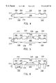
- FIG. 1 illustrates a prior art dual-chip packaging structure.
- This kind of structure has been disclosed in Japanese Laid-Open Utility Model Application No. 147360/1978 (Jitsukaisho 62-147360).
- Two chips 100 , 102 are attached to two surfaces of a die pad 104 , respectively, and connected to conductive leads 106 through bonding wires 108 .
- An encapsulant is employed to enclose the two chips 100 and 102 , inner portions of the conductive leads 106 , and the bonding wires 108 .
- a conventional leadframe is employed as a carrier in this dual-chip packaging structure, so the level of integration is limited and signal paths are relatively longer.
- a special clamping apparatus is required for attaching a second chip on the die pad and wire bonding operation. Thus, both the cost and the manufacturing complexity are increased.
- an object of the present invention is to provide a dual-chip packaging structure having a relatively high level of integration and short signal paths
- Another object of the present invention is to provide a dual-chip packaging structure having a relatively small overall packaging volume.
- Yet another object of the present invention is to provide a dual-chip packaging structure having simple manufacturing process and low cost of production.
- a dual-chip packaging structure which comprises a die pad, to each of whose two surfaces is respectively attached a chip.
- a die pad Outside and around the die pad is a plurality of first metal studs.
- a plurality of second metal studs is arranged outside and around the first metal studs. Connections between the first metal studs and the second metal studs are made by means of a plurality of conductive traces.
- the two chips on respective surfaces of the die pad are connected to corresponding ends of the first metal studs through bonding wires.
- An insulating material is employed to enclose the two chips, the die pad, the first metal studs, the conductive traces, and ends of the second metal studs, with other ends of the second metal studs exposed.
- a plurality of solder balls is attached to the respective exposed ends of the second metal studs.
- a manufacturing process for a dual-chip packaging structure which comprises a conductive substrate having a first surface, a second surface, and a die pad region. Outside and around the die pad region is a plurality of first metal stud regions. A plurality of second metal stud regions is arranged outside and around the first metal stud regions. Connections between the first metal stud regions and the second metal stud regions are made by means of a plurality of conductive trace regions. A mask layer is formed which covers the second surface, the die pad of the first surface, the first metal stud regions, the second metal stud regions, and the conductive trace regions.
- the first surface is then half etched such that the uncovered portions of the first surface are removed and a predetermined thickness is obtained.
- a first chip is attached on the die pad region of the first surface. Connections between the first chip and the first metal stud regions are made by bonding wires.
- a first insulating layer is formed which covers the first surface.
- the second surface is etched until the first insulating layer is exposed. In this instance, a die pad, first metal studs, second metal studs, and conductive traces are formed at the corresponding regions.
- a second chip is attached to the die pad of the second surface. Connections between the second chip and the first metal studs are made by the conductive traces.
- a second insulating layer is formed which covers the second surface with portions of the second metal studs of the second surface exposed. A plurality of solder balls is attached to the exposed portions of the second metal studs of the second surface.
- FIG. 1 is a schematic view of a prior art dual-chip packaging structure
- FIGS. 2 to FIG. 7 are cross-sectional views of the manufacturing process of a dual-chip package in accordance with a preferred embodiment of the present invention
- FIG. 8 is a cross-sectional view of a dual-chip packaging structure without using a plated layer in accordance with the present invention.
- FIG. 9 is a schematic view showing metal studs layout of a dual-chip packaging structure in accordance with the present invention
- FIGS. 2 to 7 show schematic, cross-sectional views of the manufacturing process of a dual-chip packaging structure in accordance with a preferred embodiment of the present invention.
- a conductive substrate 200 is provided. It is typically constructed from a material including copper, iron, copper alloy (C151, C194, C7025, KCF125, EFTEC, etc.) Ni—Fe 42 alloy or other similar matter.
- the whole conductive substrate 200 at least includes the following regions, that is, a die pad region 202 , first metal stud regions 204 , second metal stud regions 206 , and conductive trace regions 208 .
- the die pad region 202 is reserved for the fabrication of a die pad.
- the first metal stud regions 204 are arranged outside and around the die pad region 202 , which are reserved for the fabrication of first metal studs.
- the first metal studs are employed for connections to bonding pads of a die.
- the second metal stud regions 206 are arranged outside and around the first metal stud regions 204 , which are reserved for the fabrication of second metal studs.
- the second metal studs are employed for connections to solder balls.
- the conductive trace regions 208 are reserved for the fabrication of conductive traces.
- the conductive traces are employed for connections between the corresponding first metal studs and the corresponding second metal studs.
- a plated layer 210 can be formed on the first metal stud regions 204 and the second metal stud regions 206 to improve the bondability and solderability during a later manufacturing process.
- a photoresist layer 216 can be first formed on two surfaces 212 , 214 of the conductive substrate 200 . Then, by means of lithography technique, the first metal stud regions 204 and the second metal stud regions 206 are exposed.
- the plated layer 210 is then formed by either an electroplating or electrolessplating method.
- the material of the plated layer 210 includes Nickel, Palladium, Ni—Pd alloy, gold, silver and so on.
- FIG. 3 in which the photoresist layer 216 shown in FIG. 2 has been removed.
- a photolithography process is again performed to fabricate a photoresist layer 218 .
- the surface 214 is completely covered by the photoresist layer 218 , except in the first metal stud regions 204 and the second metal stud regions 206 , which are protected by the plated layer 210 .
- the photoresist layer 218 at least covers the die pad region 202 and the conductive trace regions 208 .
- FIG. 4 in which a half etching operation is performed while employing the photoresist layer 218 and the plated layer 210 shown in FIG. 3 as a mask layer.
- the exposed regions of the surface 212 are etched to a predetermined thickness D.
- the photoresist layer (item 218 in FIG. 3) is then removed.
- shapes of the die pad, the first metal studs, the second metal studs, and the conductive traces can almost be identified.
- a chip 220 is attached to the die pad region 202 of the surface 212 .
- the chip 220 includes an active surface 222 and a back surface 224 .
- the back surface 224 is adhered to the die pad region 202 of the surface 212 by means of, for example, conductive paste or insulating paste (not shown).
- the active surface 222 contains bonding pads 226 .
- Wire bonding process is performed in which connections between the bonding pads 226 and the first metal stud regions 204 of the surface 212 are made by means of bonding wires 228 .
- the bonding wires 228 are made of materials including gold, aluminum, and copper.
- a first episode of encapsulation is then performed in which the chip 220 , the first metal stud regions 204 , the second metal stud regions 206 , the conductive trace regions 208 , the bonding wires 228 , etc. of the surface 212 are all enveloped by an insulating material 230 .
- the insulating material 230 includes a resin, an epoxy, a liquid compound. and so on. Its formation includes a coating and curing process.
- FIG. 6, in which the surface 214 of the conductive substrate 200 is etched. While the surface 212 is protected by the insulating material 230 , and the first metal stud regions 204 and the second metal stud regions 206 of the surface 214 are protected by the plated layer 210 , other exposed portions of the surface 214 are etched until the insulating material 230 is exposed. That is, the predetermined thickness D is further removed.
- the die pad 232 is formed in the die pad region 202
- the first metal studs 234 are formed in the first metal stud regions 204
- the second metal studs 236 are formed in the second metal stud regions 206
- the conductive traces 238 are formed in the conductive trace regions 208 .
- a chip 240 is attached to the die pad 232 of the surface 214 .
- the chip 240 includes an active surface 242 and a back surface 244 .
- the back surface 244 is adhered to the die pad 232 of the surface 214 by means of, for example, conductive paste or insulating paste (not shown).
- the active surface 242 contains bonding pads 246 .
- a wire bonding process is performed in which connections between the bonding pads 246 and the first metal studs 234 of the surface 214 are made by means of bonding wires 248 .
- the bonding wires 248 are made of materials including gold, aluminum, and copper.
- a second episode of encapsulation is then performed in which the chip 240 , the first metal studs 234 , the conductive traces 238 , the bonding wires 248 , etc. of the surface 214 are all enveloped by an insulating material 250 , with the exception of the second metal studs 26 of the surface 214 .
- the insulating material 250 includes a resin. an epoxy, a liquid compound, etc. Its formation includes a screen printing and curing or a molding process. Attachment of solder balls is performed in which solder balls 252 are placed on the respective exposed second metal studs 236 . The solder balls 252 serve as contact points of the package to external circuitry. Materials of the solder balls 252 include tin-lead alloy. For mass production employing the manufacturing process described above, a plurality of dual-chip packages can be fabricated first on a conductive substrate simultaneously, and a trimming operation is then followed.
- FIG. 8 illustrates a dual-chip package fabricated without using plated layers. Ends of first metal stud 234 a and second metal stud 236 a are not covered by plated layers. The final thickness of them is the same as the conductive traces 238 a . Remaining manufacturing steps are similar to those described above.
- two chips are attached to two surfaces of a die pad, respectively. Bonding pads of the two chips are connected to corresponding ends of first metal studs by bonding wires. The two surfaces are enclosed by insulating materials which covered the two chips, the first metal studs the bonding wires, conductive traces, and one end of each second metal stud. The other end of each second metal stud is exposed, on which end a solder ball is attached.
- FIG. 9 where the layout of metal studs in a dual-chip package is schematically illustrated.
- a die pad 232 is located in the center for chip attachment.
- First metal studs 234 are located outside the die pad and surrounding it, and are connected to bonding pads on the chip.
- Second metal studs 236 are located outside the first metal studs in an area array arrangement and attached with solder balls.
- Conductive traces 238 are respectively connected to the corresponding first metal studs 234 and the corresponding second metal studs 236 .
- the dual-chip packaging structure and manufacturing process in accordance with the present invention at least includes the following advantages.
- an etching technique is employed for fabrications of metal studs and conductive traces. Pitch is then relatively small, and hence, an overall volume of the package can be reduced.
Landscapes
- Engineering & Computer Science (AREA)
- Physics & Mathematics (AREA)
- Condensed Matter Physics & Semiconductors (AREA)
- General Physics & Mathematics (AREA)
- Computer Hardware Design (AREA)
- Microelectronics & Electronic Packaging (AREA)
- Power Engineering (AREA)
- Manufacturing & Machinery (AREA)
- Lead Frames For Integrated Circuits (AREA)
Abstract
A dual-chip packaging structure comprises a die pad with a chip attached to each of its two surfaces. Outside and around the die pad is a plurality of first metal studs. A plurality of second metal studs is arranged outside and around the first metal studs. Connections between the first metal studs and the second metal studs are made by means of a plurality of conductive traces. The two chips on the respective surfaces of the die pad are connected to corresponding ends of the first metal studs through bonding wires. An insulating material is employed to enclose the two chips, the die pad, the first metal studs, the conductive traces, and ends of the second metal studs, with other ends of the second metal studs exposed. A plurality of solder balls is attached to the respective exposed ends of the second metal studs.
Description
1. Field of Invention
The present invention relates to a manufacturing process and structure of a dualchip package. More particularly, the present invention relates to a dual-chip package in which metal studs and solder balls are employed as connection media to external circuitry.
2. Description of Related Art
High performance, high level of integration, low cost, increased miniaturization of components and devices are all the common goals in the semiconductor design and manufacture. Mass production of 0.18 microns semiconductor devices are currently achieved and its integration level need not be emphasized. However, higher carrier density, smaller in overall volume, etc. are still main concerns for having high integration level of electronic packaging. Indeed, no matter whether on computers or general commodities, in order to reduce the overall size and the cost, a technique of putting two or more individual chips in a single package has been developed. This kind of packaging will be mainstream in the future. Multichip packaging can be employed to integrate processors and memory chips, or Logic chips and memory chips (including DRAMs, Flash memories, etc.) in a single package. Thus, the cost and the overall size are reduced. Moreover, signal transmission distances can be shortened, and hence, the performance is enhanced. In addition, different individual chips with different fabrication processes can be put together in a single package and no special integration manufacturing processes is required.
Reference is made to FIG. 1, which illustrates a prior art dual-chip packaging structure. This kind of structure has been disclosed in Japanese Laid-Open Utility Model Application No. 147360/1978 (Jitsukaisho 62-147360). Two chips 100, 102 are attached to two surfaces of a die pad 104, respectively, and connected to conductive leads 106 through bonding wires 108. An encapsulant is employed to enclose the two chips 100 and 102, inner portions of the conductive leads 106, and the bonding wires 108. However, a conventional leadframe is employed as a carrier in this dual-chip packaging structure, so the level of integration is limited and signal paths are relatively longer. Moreover, after a first chip is attached on the die pad and wire bonding is completed, a special clamping apparatus is required for attaching a second chip on the die pad and wire bonding operation. Thus, both the cost and the manufacturing complexity are increased.
Accordingly, an object of the present invention is to provide a dual-chip packaging structure having a relatively high level of integration and short signal paths
Another object of the present invention is to provide a dual-chip packaging structure having a relatively small overall packaging volume.
Yet another object of the present invention is to provide a dual-chip packaging structure having simple manufacturing process and low cost of production.
To achieve these objects and other advantages and in accordance with the present invention, a dual-chip packaging structure is described herein, which comprises a die pad, to each of whose two surfaces is respectively attached a chip. Outside and around the die pad is a plurality of first metal studs. A plurality of second metal studs is arranged outside and around the first metal studs. Connections between the first metal studs and the second metal studs are made by means of a plurality of conductive traces. The two chips on respective surfaces of the die pad are connected to corresponding ends of the first metal studs through bonding wires. An insulating material is employed to enclose the two chips, the die pad, the first metal studs, the conductive traces, and ends of the second metal studs, with other ends of the second metal studs exposed. A plurality of solder balls is attached to the respective exposed ends of the second metal studs.
To achieve these objects and other advantages and in accordance with the present invention, a manufacturing process for a dual-chip packaging structure is described herein, which comprises a conductive substrate having a first surface, a second surface, and a die pad region. Outside and around the die pad region is a plurality of first metal stud regions. A plurality of second metal stud regions is arranged outside and around the first metal stud regions. Connections between the first metal stud regions and the second metal stud regions are made by means of a plurality of conductive trace regions. A mask layer is formed which covers the second surface, the die pad of the first surface, the first metal stud regions, the second metal stud regions, and the conductive trace regions. The first surface is then half etched such that the uncovered portions of the first surface are removed and a predetermined thickness is obtained. A first chip is attached on the die pad region of the first surface. Connections between the first chip and the first metal stud regions are made by bonding wires. A first insulating layer is formed which covers the first surface. The second surface is etched until the first insulating layer is exposed. In this instance, a die pad, first metal studs, second metal studs, and conductive traces are formed at the corresponding regions. A second chip is attached to the die pad of the second surface. Connections between the second chip and the first metal studs are made by the conductive traces. A second insulating layer is formed which covers the second surface with portions of the second metal studs of the second surface exposed. A plurality of solder balls is attached to the exposed portions of the second metal studs of the second surface.
It is to be understood that both the foregoing general description and the following detailed description are exemplary, and are intended to provide further explanation of the invention as claimed.
The accompanying drawings are included to provide a further understanding of the invention, and are incorporated in and constitute a part of this specification. The drawings illustrate embodiments of the invention and, together with the description, serve to explain the principles of the invention. In the drawings,
FIG. 1 is a schematic view of a prior art dual-chip packaging structure;
FIGS. 2 to FIG. 7 are cross-sectional views of the manufacturing process of a dual-chip package in accordance with a preferred embodiment of the present invention;
FIG. 8 is a cross-sectional view of a dual-chip packaging structure without using a plated layer in accordance with the present invention; and
FIG. 9 is a schematic view showing metal studs layout of a dual-chip packaging structure in accordance with the present invention
Reference is made to FIGS. 2 to 7, which show schematic, cross-sectional views of the manufacturing process of a dual-chip packaging structure in accordance with a preferred embodiment of the present invention. As shown in FIG. 2, a conductive substrate 200 is provided. It is typically constructed from a material including copper, iron, copper alloy (C151, C194, C7025, KCF125, EFTEC, etc.) Ni—Fe 42 alloy or other similar matter. The whole conductive substrate 200 at least includes the following regions, that is, a die pad region 202, first metal stud regions 204, second metal stud regions 206, and conductive trace regions 208. The die pad region 202 is reserved for the fabrication of a die pad. The first metal stud regions 204 are arranged outside and around the die pad region 202, which are reserved for the fabrication of first metal studs. The first metal studs are employed for connections to bonding pads of a die. The second metal stud regions 206 are arranged outside and around the first metal stud regions 204, which are reserved for the fabrication of second metal studs. The second metal studs are employed for connections to solder balls. The conductive trace regions 208 are reserved for the fabrication of conductive traces. The conductive traces are employed for connections between the corresponding first metal studs and the corresponding second metal studs. A plated layer 210 can be formed on the first metal stud regions 204 and the second metal stud regions 206 to improve the bondability and solderability during a later manufacturing process. For example, a photoresist layer 216 can be first formed on two surfaces 212, 214 of the conductive substrate 200. Then, by means of lithography technique, the first metal stud regions 204 and the second metal stud regions 206 are exposed. The plated layer 210 is then formed by either an electroplating or electrolessplating method. The material of the plated layer 210 includes Nickel, Palladium, Ni—Pd alloy, gold, silver and so on.
Reference is made to FIG. 3 in which the photoresist layer 216 shown in FIG. 2 has been removed. A photolithography process is again performed to fabricate a photoresist layer 218. At this episode, the surface 214 is completely covered by the photoresist layer 218, except in the first metal stud regions 204 and the second metal stud regions 206, which are protected by the plated layer 210. On the surface 212, the photoresist layer 218 at least covers the die pad region 202 and the conductive trace regions 208.
Reference is made to FIG. 4, in which a half etching operation is performed while employing the photoresist layer 218 and the plated layer 210 shown in FIG. 3 as a mask layer. The exposed regions of the surface 212 are etched to a predetermined thickness D. The photoresist layer (item 218 in FIG. 3) is then removed. In this instance, shapes of the die pad, the first metal studs, the second metal studs, and the conductive traces can almost be identified.
Reference is made to FIG. 5, in which a first episode of die attachment and wire bonding processes is performed. A chip 220 is attached to the die pad region 202 of the surface 212. The chip 220 includes an active surface 222 and a back surface 224. The back surface 224 is adhered to the die pad region 202 of the surface 212 by means of, for example, conductive paste or insulating paste (not shown). The active surface 222 contains bonding pads 226. Wire bonding process is performed in which connections between the bonding pads 226 and the first metal stud regions 204 of the surface 212 are made by means of bonding wires 228. The bonding wires 228 are made of materials including gold, aluminum, and copper. A first episode of encapsulation is then performed in which the chip 220, the first metal stud regions 204, the second metal stud regions 206, the conductive trace regions 208, the bonding wires 228, etc. of the surface 212 are all enveloped by an insulating material 230. The insulating material 230 includes a resin, an epoxy, a liquid compound. and so on. Its formation includes a coating and curing process.
Reference is made to FIG. 6, in which the surface 214 of the conductive substrate 200 is etched. While the surface 212 is protected by the insulating material 230, and the first metal stud regions 204 and the second metal stud regions 206 of the surface 214 are protected by the plated layer 210, other exposed portions of the surface 214 are etched until the insulating material 230 is exposed. That is, the predetermined thickness D is further removed. In this instance, the die pad 232 is formed in the die pad region 202, the first metal studs 234 are formed in the first metal stud regions 204, the second metal studs 236 are formed in the second metal stud regions 206, and the conductive traces 238 are formed in the conductive trace regions 208.
Reference is made to FIG. 7, in which a second episode of die attachment and wire bonding processes is performed. A chip 240 is attached to the die pad 232 of the surface 214. The chip 240 includes an active surface 242 and a back surface 244. The back surface 244 is adhered to the die pad 232 of the surface 214 by means of, for example, conductive paste or insulating paste (not shown). The active surface 242 contains bonding pads 246. A wire bonding process is performed in which connections between the bonding pads 246 and the first metal studs 234 of the surface 214 are made by means of bonding wires 248. The bonding wires 248 are made of materials including gold, aluminum, and copper. A second episode of encapsulation is then performed in which the chip 240, the first metal studs 234, the conductive traces 238, the bonding wires 248, etc. of the surface 214 are all enveloped by an insulating material 250, with the exception of the second metal studs 26 of the surface 214. The insulating material 250 includes a resin. an epoxy, a liquid compound, etc. Its formation includes a screen printing and curing or a molding process. Attachment of solder balls is performed in which solder balls 252 are placed on the respective exposed second metal studs 236. The solder balls 252 serve as contact points of the package to external circuitry. Materials of the solder balls 252 include tin-lead alloy. For mass production employing the manufacturing process described above, a plurality of dual-chip packages can be fabricated first on a conductive substrate simultaneously, and a trimming operation is then followed.
Alternately, another manufacturing process according to the present invention is available. For example, the plated layer 210 described above can be replaced by a photoresist layer and then serves as a mask layer. Thereby, the final thickness of metal studs is thinner as shown in FIG. 8. Reference is now made to FIG. 8, which illustrates a dual-chip package fabricated without using plated layers. Ends of first metal stud 234 a and second metal stud 236 a are not covered by plated layers. The final thickness of them is the same as the conductive traces 238 a. Remaining manufacturing steps are similar to those described above.
In the dual-chip packaging structure according to the present invention, two chips are attached to two surfaces of a die pad, respectively. Bonding pads of the two chips are connected to corresponding ends of first metal studs by bonding wires. The two surfaces are enclosed by insulating materials which covered the two chips, the first metal studs the bonding wires, conductive traces, and one end of each second metal stud. The other end of each second metal stud is exposed, on which end a solder ball is attached.
Further description of the manufacturing process according to the present invention is given as follows. The arrangement of the second metal studs described above are in peripheral layout. However, in order to increase the level of integration and adapted to high lead-count devices, an area array arrangement can be employed for the second metal studs as shown in FIG. 9, where the layout of metal studs in a dual-chip package is schematically illustrated. Therein, a die pad 232 is located in the center for chip attachment. First metal studs 234 are located outside the die pad and surrounding it, and are connected to bonding pads on the chip. Second metal studs 236 are located outside the first metal studs in an area array arrangement and attached with solder balls. Conductive traces 238 are respectively connected to the corresponding first metal studs 234 and the corresponding second metal studs 236.
Based on the foregoing, the dual-chip packaging structure and manufacturing process in accordance with the present invention at least includes the following advantages.
1. In the dual-chip packaging structure in accordance with the present invention, two individual chips are integrated in a single package. Because an area array configuration can be employed herein, the level of integration is relatively higher. Metal studs, conductive traces, and solder balls are used as connection media to external circuitry, and hence, signal paths are relatively short and the performance of the package can be enhanced.
2. In the dual-chip packaging structure in accordance with the present invention, an etching technique is employed for fabrications of metal studs and conductive traces. Pitch is then relatively small, and hence, an overall volume of the package can be reduced.
3. In the dual-chip packaging structure in accordance with the present invention, integration of carrier formation process (including formations of a die pad, metal studs, and conductive traces) and assembly process (including die attachment, wire bonding, encapsulating, etc.) is established. T hereby, the manufacturing process is simplified and the production cost is reduced.
It will be apparent to those skilled in the art that various modifications and variations can be made to the structure of the present invention without departing from the scope or spirit of the invention. In view of the foregoing, it is intended that the present invention cover modifications and variations of this invention provided they fall within the scope of the following claims and their equivalents.
Claims (21)
1. A dual-chip package, comprising:
a die pad;
a plurality of first metal studs located around the die pad;
a plurality of second metal studs around the first metal studs;
a plurality of conductive traces electrically connecting the first metal studs and the second metal studs;
a first chip attached to a top surface of the die pad and electrically connected to respective top ends of the first metal studs;
a second chip attached to a bottom surface of the die pad and electrically connected to respective bottom ends of the first metal studs; and
an insulating material sealing the first chip, the second chip, the connection between the first chip and the first metal studs, the connection between the second chip and the first metal studs, and the conductive traces, wherein the first studs are entirely enclosed, leaving only one end of each second stud exposed for external connection.
2. The dual-chip package of claim 1 , wherein the two ends of the first metal studs include plated layers.
3. The dual-chip package of claim 1 , wherein the other ends of the second metal studs includes plated layers.
4. The dual-chip package of claim 1 , wherein the electrical connections between the first bonding pads and the ends of the first metal studs are established by bonding wires.
5. The dual-chip package of claim 1 , wherein the electrical connections between the second bonding pads and the other ends of the first metal studs are established by bonding wires.
6. The package of claim 1 , wherein the first and second metal studs are thicker than the conductive traces.
7. The Package of claim 1 , wherein the first and second metal studs have substantially the same thickness as the conductive traces.
8. The package of claim 1 , further comprising a plurality of solder balls respectively located on the exposed ends of the second metal studs.
9. A method of manufacturing a dual-chip package, comprising the steps of:
providing a conductive substrate;
defining a die pad region, a first metal stud region and a second metal stud region on a top surface of the substrate, wherein the first metal stud region is located around the die pad region, and the second metal stud region is spaced from and around the first stud region;
attaching a first chip onto the die pad region and electrically connecting the first chip to the first metal stud regions;
forming a first insulating layer over the top surface of the conductive substrate, the first chip, and the connections between the first chip and the first metal stud regions;
removing a bottom surface of the conductive substrate until the first insulating layer is exposed, such that a die pad having a bottom surface is formed in the die pad region, a plurality of first metal studs are formed in the first metal stud region, a plurality of second metal studs arc formed in the second metal stud region, and a plurality of conductive traces are formed between the first metal studs and the second metal studs;
attaching the second chip to the bottom surface of the die pad and electrically connecting the second chip to the first metal studs; and
forming a second insulating layer over the second surface of the conductive substrate, the second chip, and the connections between the second chip and the first metal studs, leaving one end of each of the second metal studs exposed for external connection.
10. The method of claim 9 , further comprising:
forming a plated layer on the first metal stud regions and the second metal stud regions.
11. The method of claim 9 , wherein the first insulating layer is formed of a liquid compound.
12. The method of claim 9 , wherein a process of forming the second insulating layer is achieved by a screen printing method.
13. The method of claim 9 , wherein a process of forming the second insulating layer is achieved by a molding method.
14. The method of claim 9 , wherein the first chip includes an active surface and a back surface, with the active surface having a plurality of bonding pads and the back surface attached to the die pad region, and wherein a plurality of bonding wires is employed to connect the bonding pads and the first metal stud regions.
15. The method of claim 9 , wherein the second chip includes an active surface and a back surface, with the active surface having a plurality of bonding pads and the back surface attached to the die pad, and wherein a plurality of bonding wires is employed to connect the bonding pads and the first metal studs.
16. The method of claim 9 , wherein defining the die pad region, a first metal stud region and a second metal stud region is achieved by half etching the conductive substrate to remove portions of the conductive substrate along the first surface uncovered by the mask layer until a predetermined thickness.
17. The method of claim 9 , wherein the conductive traces have the same thickness or different thickness from the first metal studs.
18. The method of claim 9 , further comprising the step of placing a plurality of solder balls on the exposed ends of the second metal studs.
19. A dual-chip package, comprising:
a die pad having a first surface and a second surface;
a first chip located on the first surface of the die pad;
a second chip located on the second surface of the die pad;
a plurality of first metal studs located around the die pad;
a plurality of second metal studs spaced from and around the first metal studs;
a plurality of conductive traces electrically connecting the first metal studs and the second metal studs;
an insulating material sealing the first chip, the second chip, the connections between the chips and the metal studs, the conductive traces, the first metal studs, and one end of each second metal stud; and
a plurality of solder balls located respectively to the top ends of the second metal studs.
20. The package of claim 19 , wherein the die pad is located substantially the same level as the conductive traces.
21. The package of claim 19 , wherein the first and second metal studs further have plated layers on their ends.
Priority Applications (1)
| Application Number | Priority Date | Filing Date | Title |
|---|---|---|---|
| US09/470,188 US6344687B1 (en) | 1999-12-22 | 1999-12-22 | Dual-chip packaging |
Applications Claiming Priority (1)
| Application Number | Priority Date | Filing Date | Title |
|---|---|---|---|
| US09/470,188 US6344687B1 (en) | 1999-12-22 | 1999-12-22 | Dual-chip packaging |
Publications (1)
| Publication Number | Publication Date |
|---|---|
| US6344687B1 true US6344687B1 (en) | 2002-02-05 |
Family
ID=23866611
Family Applications (1)
| Application Number | Title | Priority Date | Filing Date |
|---|---|---|---|
| US09/470,188 Expired - Fee Related US6344687B1 (en) | 1999-12-22 | 1999-12-22 | Dual-chip packaging |
Country Status (1)
| Country | Link |
|---|---|
| US (1) | US6344687B1 (en) |
Cited By (13)
| Publication number | Priority date | Publication date | Assignee | Title |
|---|---|---|---|---|
| US20030085463A1 (en) * | 2001-11-08 | 2003-05-08 | Gerber Mark A. | Semiconductor package device for use with multiple integrated circuits in a stacked configuration and method fo formation and testing |
| US6777786B2 (en) * | 2001-03-12 | 2004-08-17 | Fairchild Semiconductor Corporation | Semiconductor device including stacked dies mounted on a leadframe |
| US6858922B2 (en) * | 2001-01-19 | 2005-02-22 | International Rectifier Corporation | Back-to-back connected power semiconductor device package |
| WO2007008171A2 (en) * | 2005-07-09 | 2007-01-18 | Gautham Viswanadam | Integrated circuit device and method of manufacturing thereof |
| US20070057367A1 (en) * | 2001-07-10 | 2007-03-15 | Samsung Electronics Co., Ltd. | Semiconductor chip having bond pads and multi-chip package |
| US20090001554A1 (en) * | 2007-06-26 | 2009-01-01 | Infineon Technologies Ag | Semiconductor device |
| US20090001563A1 (en) * | 2007-06-27 | 2009-01-01 | Henry Descalzo Bathan | Integrated circuit package in package system with adhesiveless package attach |
| US20100086727A1 (en) * | 2005-07-29 | 2010-04-08 | The Doshisha | Method for molding fiber-reinforced thermoplastic composite material, intermediate thereof and composite sheet |
| US20120012993A1 (en) * | 2008-01-09 | 2012-01-19 | Yong Liu | Die package including substrate with molded device |
| US20140227835A1 (en) * | 2010-05-20 | 2014-08-14 | Qualcomm Incorporated | Process for improving package warpage and connection reliability through use of a backside mold configuration (bsmc) |
| US10755940B2 (en) * | 2015-09-30 | 2020-08-25 | Texas Instruments Incorporated | Plating interconnect for silicon chip |
| CN112548370A (en) * | 2019-09-26 | 2021-03-26 | 泰连德国有限公司 | Welding method |
| US11227807B2 (en) * | 2018-11-16 | 2022-01-18 | Hewlett-Packard Development Company, L.P. | Two-step molding for a lead frame |
Citations (6)
| Publication number | Priority date | Publication date | Assignee | Title |
|---|---|---|---|---|
| US5545922A (en) * | 1994-06-28 | 1996-08-13 | Intel Corporation | Dual sided integrated circuit chip package with offset wire bonds and support block cavities |
| US5596225A (en) * | 1994-10-27 | 1997-01-21 | National Semiconductor Corporation | Leadframe for an integrated circuit package which electrically interconnects multiple integrated circuit die |
| US5818102A (en) * | 1995-12-29 | 1998-10-06 | Lsi Logic Corporation | System having integrated circuit package with lead frame having internal power and ground busses |
| US5889325A (en) * | 1996-07-25 | 1999-03-30 | Nec Corporation | Semiconductor device and method of manufacturing the same |
| US5905639A (en) * | 1997-09-29 | 1999-05-18 | Raytheon Company | Three-dimensional component stacking using high density multichip interconnect decals and three-bond daisy-chained wedge bonds |
| US6153928A (en) * | 1996-05-17 | 2000-11-28 | Hyuandai Electronics Industries Co., Ltd. | Substrate for semiconductor package, fabrication method thereof, and stacked-type semiconductor package using the substrate |
-
1999
- 1999-12-22 US US09/470,188 patent/US6344687B1/en not_active Expired - Fee Related
Patent Citations (6)
| Publication number | Priority date | Publication date | Assignee | Title |
|---|---|---|---|---|
| US5545922A (en) * | 1994-06-28 | 1996-08-13 | Intel Corporation | Dual sided integrated circuit chip package with offset wire bonds and support block cavities |
| US5596225A (en) * | 1994-10-27 | 1997-01-21 | National Semiconductor Corporation | Leadframe for an integrated circuit package which electrically interconnects multiple integrated circuit die |
| US5818102A (en) * | 1995-12-29 | 1998-10-06 | Lsi Logic Corporation | System having integrated circuit package with lead frame having internal power and ground busses |
| US6153928A (en) * | 1996-05-17 | 2000-11-28 | Hyuandai Electronics Industries Co., Ltd. | Substrate for semiconductor package, fabrication method thereof, and stacked-type semiconductor package using the substrate |
| US5889325A (en) * | 1996-07-25 | 1999-03-30 | Nec Corporation | Semiconductor device and method of manufacturing the same |
| US5905639A (en) * | 1997-09-29 | 1999-05-18 | Raytheon Company | Three-dimensional component stacking using high density multichip interconnect decals and three-bond daisy-chained wedge bonds |
Cited By (23)
| Publication number | Priority date | Publication date | Assignee | Title |
|---|---|---|---|---|
| US6858922B2 (en) * | 2001-01-19 | 2005-02-22 | International Rectifier Corporation | Back-to-back connected power semiconductor device package |
| US6777786B2 (en) * | 2001-03-12 | 2004-08-17 | Fairchild Semiconductor Corporation | Semiconductor device including stacked dies mounted on a leadframe |
| US20050001293A1 (en) * | 2001-03-12 | 2005-01-06 | Fairchild Semiconductor Corporation | Method for forming semiconductor device including stacked dies |
| US7071033B2 (en) | 2001-03-12 | 2006-07-04 | Fairchild Semiconductor Corporation | Method for forming semiconductor device including stacked dies |
| US7576440B2 (en) * | 2001-07-10 | 2009-08-18 | Samsung Electronics Co., Ltd. | Semiconductor chip having bond pads and multi-chip package |
| US20070057367A1 (en) * | 2001-07-10 | 2007-03-15 | Samsung Electronics Co., Ltd. | Semiconductor chip having bond pads and multi-chip package |
| US6916682B2 (en) * | 2001-11-08 | 2005-07-12 | Freescale Semiconductor, Inc. | Semiconductor package device for use with multiple integrated circuits in a stacked configuration and method of formation and testing |
| US20030085463A1 (en) * | 2001-11-08 | 2003-05-08 | Gerber Mark A. | Semiconductor package device for use with multiple integrated circuits in a stacked configuration and method fo formation and testing |
| US7785928B2 (en) | 2005-07-09 | 2010-08-31 | Gautham Viswanadam | Integrated circuit device and method of manufacturing thereof |
| WO2007008171A2 (en) * | 2005-07-09 | 2007-01-18 | Gautham Viswanadam | Integrated circuit device and method of manufacturing thereof |
| WO2007008171A3 (en) * | 2005-07-09 | 2007-06-07 | Gautham Viswanadam | Integrated circuit device and method of manufacturing thereof |
| US20100144093A1 (en) * | 2005-07-09 | 2010-06-10 | Gautham Viswanadam | Integrated Circuit Device and Method of Manufacturing Thereof |
| US20100086727A1 (en) * | 2005-07-29 | 2010-04-08 | The Doshisha | Method for molding fiber-reinforced thermoplastic composite material, intermediate thereof and composite sheet |
| US7683477B2 (en) * | 2007-06-26 | 2010-03-23 | Infineon Technologies Ag | Semiconductor device including semiconductor chips having contact elements |
| US20090001554A1 (en) * | 2007-06-26 | 2009-01-01 | Infineon Technologies Ag | Semiconductor device |
| US20090001563A1 (en) * | 2007-06-27 | 2009-01-01 | Henry Descalzo Bathan | Integrated circuit package in package system with adhesiveless package attach |
| US8203214B2 (en) * | 2007-06-27 | 2012-06-19 | Stats Chippac Ltd. | Integrated circuit package in package system with adhesiveless package attach |
| US20120012993A1 (en) * | 2008-01-09 | 2012-01-19 | Yong Liu | Die package including substrate with molded device |
| US8525192B2 (en) * | 2008-01-09 | 2013-09-03 | Fairchild Semiconductor Corporation | Die package including substrate with molded device |
| US20140227835A1 (en) * | 2010-05-20 | 2014-08-14 | Qualcomm Incorporated | Process for improving package warpage and connection reliability through use of a backside mold configuration (bsmc) |
| US10755940B2 (en) * | 2015-09-30 | 2020-08-25 | Texas Instruments Incorporated | Plating interconnect for silicon chip |
| US11227807B2 (en) * | 2018-11-16 | 2022-01-18 | Hewlett-Packard Development Company, L.P. | Two-step molding for a lead frame |
| CN112548370A (en) * | 2019-09-26 | 2021-03-26 | 泰连德国有限公司 | Welding method |
Similar Documents
| Publication | Publication Date | Title |
|---|---|---|
| US6507120B2 (en) | Flip chip type quad flat non-leaded package | |
| US6762118B2 (en) | Package having array of metal pegs linked by printed circuit lines | |
| US6878570B2 (en) | Thin stacked package and manufacturing method thereof | |
| US6818976B2 (en) | Bumped chip carrier package using lead frame | |
| US6388313B1 (en) | Multi-chip module | |
| US8241967B2 (en) | Semiconductor package with a support structure and fabrication method thereof | |
| KR100498488B1 (en) | Stacked semiconductor package and fabricating method the same | |
| US7834469B2 (en) | Stacked type chip package structure including a chip package and a chip that are stacked on a lead frame | |
| US20090278243A1 (en) | Stacked type chip package structure and method for fabricating the same | |
| US6876087B2 (en) | Chip scale package with heat dissipating part | |
| US6429043B1 (en) | Semiconductor circuitry device and method for manufacturing the same | |
| US6344687B1 (en) | Dual-chip packaging | |
| US20080308951A1 (en) | Semiconductor package and fabrication method thereof | |
| US6894904B2 (en) | Tab package | |
| US20040188818A1 (en) | Multi-chips module package | |
| KR100394030B1 (en) | stack-type semiconductor package | |
| US20030042583A1 (en) | Quad flat non-leaded semiconductor package and method of fabricating the same | |
| US7015591B2 (en) | Exposed pad module integrating a passive device therein | |
| US7173341B2 (en) | High performance thermally enhanced package and method of fabricating the same | |
| US8395246B2 (en) | Two-sided die in a four-sided leadframe based package | |
| US6380062B1 (en) | Method of fabricating semiconductor package having metal peg leads and connected by trace lines | |
| US8349655B2 (en) | Method of fabricating a two-sided die in a four-sided leadframe based package | |
| US20010001069A1 (en) | Metal stud array packaging | |
| KR100247641B1 (en) | Package and method of manufacturing the same | |
| US7078798B2 (en) | Semiconductor package and manufacturing method thereof |
Legal Events
| Date | Code | Title | Description |
|---|---|---|---|
| FPAY | Fee payment |
Year of fee payment: 4 |
|
| REMI | Maintenance fee reminder mailed | ||
| LAPS | Lapse for failure to pay maintenance fees | ||
| LAPS | Lapse for failure to pay maintenance fees |
Free format text: PATENT EXPIRED FOR FAILURE TO PAY MAINTENANCE FEES (ORIGINAL EVENT CODE: EXP.); ENTITY STATUS OF PATENT OWNER: SMALL ENTITY |
|
| STCH | Information on status: patent discontinuation |
Free format text: PATENT EXPIRED DUE TO NONPAYMENT OF MAINTENANCE FEES UNDER 37 CFR 1.362 |
|
| FP | Lapsed due to failure to pay maintenance fee |
Effective date: 20100205 |