US6379989B1 - Process for manufacture of microoptomechanical structures - Google Patents
Process for manufacture of microoptomechanical structures Download PDFInfo
- Publication number
- US6379989B1 US6379989B1 US09/468,141 US46814199A US6379989B1 US 6379989 B1 US6379989 B1 US 6379989B1 US 46814199 A US46814199 A US 46814199A US 6379989 B1 US6379989 B1 US 6379989B1
- Authority
- US
- United States
- Prior art keywords
- layer
- crystal silicon
- depositing
- single crystal
- silicon layer
- Prior art date
- Legal status (The legal status is an assumption and is not a legal conclusion. Google has not performed a legal analysis and makes no representation as to the accuracy of the status listed.)
- Expired - Lifetime
Links
- 238000000034 method Methods 0.000 title claims description 47
- 230000008569 process Effects 0.000 title claims description 26
- 238000004519 manufacturing process Methods 0.000 title description 10
- 229910021421 monocrystalline silicon Inorganic materials 0.000 claims abstract description 42
- 229910021420 polycrystalline silicon Inorganic materials 0.000 claims abstract description 34
- 229920005591 polysilicon Polymers 0.000 claims abstract description 32
- 238000000151 deposition Methods 0.000 claims abstract description 30
- XUIMIQQOPSSXEZ-UHFFFAOYSA-N Silicon Chemical compound [Si] XUIMIQQOPSSXEZ-UHFFFAOYSA-N 0.000 claims abstract description 23
- 229910052710 silicon Inorganic materials 0.000 claims abstract description 22
- 239000010703 silicon Substances 0.000 claims abstract description 22
- 238000005530 etching Methods 0.000 claims abstract description 20
- 239000012212 insulator Substances 0.000 claims abstract description 14
- 239000010409 thin film Substances 0.000 claims description 21
- 230000003287 optical effect Effects 0.000 claims description 20
- 239000013078 crystal Substances 0.000 claims description 12
- 238000000059 patterning Methods 0.000 claims description 12
- 238000001312 dry etching Methods 0.000 claims description 3
- 239000012788 optical film Substances 0.000 claims 3
- 239000011248 coating agent Substances 0.000 claims 1
- 238000000576 coating method Methods 0.000 claims 1
- 230000001681 protective effect Effects 0.000 claims 1
- 235000012431 wafers Nutrition 0.000 description 25
- XLYOFNOQVPJJNP-UHFFFAOYSA-N water Chemical compound O XLYOFNOQVPJJNP-UHFFFAOYSA-N 0.000 description 23
- 238000005459 micromachining Methods 0.000 description 17
- FFUAGWLWBBFQJT-UHFFFAOYSA-N hexamethyldisilazane Chemical compound C[Si](C)(C)N[Si](C)(C)C FFUAGWLWBBFQJT-UHFFFAOYSA-N 0.000 description 13
- 229920002120 photoresistant polymer Polymers 0.000 description 13
- 238000000206 photolithography Methods 0.000 description 9
- 238000005229 chemical vapour deposition Methods 0.000 description 8
- 238000004518 low pressure chemical vapour deposition Methods 0.000 description 8
- 239000000463 material Substances 0.000 description 8
- 150000004767 nitrides Chemical class 0.000 description 8
- 239000000758 substrate Substances 0.000 description 8
- 239000007943 implant Substances 0.000 description 7
- 238000000708 deep reactive-ion etching Methods 0.000 description 6
- 230000008021 deposition Effects 0.000 description 6
- 238000013461 design Methods 0.000 description 6
- 239000005360 phosphosilicate glass Substances 0.000 description 6
- 238000001020 plasma etching Methods 0.000 description 6
- ZOXJGFHDIHLPTG-UHFFFAOYSA-N Boron Chemical compound [B] ZOXJGFHDIHLPTG-UHFFFAOYSA-N 0.000 description 5
- 229910052796 boron Inorganic materials 0.000 description 5
- 239000002019 doping agent Substances 0.000 description 5
- 238000005516 engineering process Methods 0.000 description 5
- XPDWGBQVDMORPB-UHFFFAOYSA-N Fluoroform Chemical compound FC(F)F XPDWGBQVDMORPB-UHFFFAOYSA-N 0.000 description 4
- 230000008901 benefit Effects 0.000 description 4
- 239000012528 membrane Substances 0.000 description 4
- 238000012545 processing Methods 0.000 description 4
- 102100029376 Cryptochrome-1 Human genes 0.000 description 3
- 101000919351 Homo sapiens Cryptochrome-1 Proteins 0.000 description 3
- 238000000347 anisotropic wet etching Methods 0.000 description 3
- 230000004888 barrier function Effects 0.000 description 3
- 238000002310 reflectometry Methods 0.000 description 3
- NBIIXXVUZAFLBC-UHFFFAOYSA-N Phosphoric acid Chemical compound OP(O)(O)=O NBIIXXVUZAFLBC-UHFFFAOYSA-N 0.000 description 2
- OAICVXFJPJFONN-UHFFFAOYSA-N Phosphorus Chemical compound [P] OAICVXFJPJFONN-UHFFFAOYSA-N 0.000 description 2
- VYPSYNLAJGMNEJ-UHFFFAOYSA-N Silicium dioxide Chemical compound O=[Si]=O VYPSYNLAJGMNEJ-UHFFFAOYSA-N 0.000 description 2
- 229910052782 aluminium Inorganic materials 0.000 description 2
- XAGFODPZIPBFFR-UHFFFAOYSA-N aluminium Chemical compound [Al] XAGFODPZIPBFFR-UHFFFAOYSA-N 0.000 description 2
- 230000001419 dependent effect Effects 0.000 description 2
- 238000009501 film coating Methods 0.000 description 2
- 238000004377 microelectronic Methods 0.000 description 2
- 238000012986 modification Methods 0.000 description 2
- 230000004048 modification Effects 0.000 description 2
- 238000004806 packaging method and process Methods 0.000 description 2
- 229910052698 phosphorus Inorganic materials 0.000 description 2
- 239000011574 phosphorus Substances 0.000 description 2
- 238000012805 post-processing Methods 0.000 description 2
- 238000000427 thin-film deposition Methods 0.000 description 2
- 238000001039 wet etching Methods 0.000 description 2
- 238000002120 advanced silicon etching Methods 0.000 description 1
- 229910000147 aluminium phosphate Inorganic materials 0.000 description 1
- 238000000137 annealing Methods 0.000 description 1
- 239000003990 capacitor Substances 0.000 description 1
- 229910052681 coesite Inorganic materials 0.000 description 1
- 230000000295 complement effect Effects 0.000 description 1
- 229910052906 cristobalite Inorganic materials 0.000 description 1
- 239000003989 dielectric material Substances 0.000 description 1
- 230000005496 eutectics Effects 0.000 description 1
- 239000010408 film Substances 0.000 description 1
- 230000012447 hatching Effects 0.000 description 1
- 230000002209 hydrophobic effect Effects 0.000 description 1
- 238000010348 incorporation Methods 0.000 description 1
- 230000010354 integration Effects 0.000 description 1
- 238000010884 ion-beam technique Methods 0.000 description 1
- 229910052751 metal Inorganic materials 0.000 description 1
- 239000002184 metal Substances 0.000 description 1
- 229910044991 metal oxide Inorganic materials 0.000 description 1
- 150000004706 metal oxides Chemical class 0.000 description 1
- 239000000615 nonconductor Substances 0.000 description 1
- 230000003647 oxidation Effects 0.000 description 1
- 238000007254 oxidation reaction Methods 0.000 description 1
- 238000002161 passivation Methods 0.000 description 1
- 210000002381 plasma Anatomy 0.000 description 1
- 238000005498 polishing Methods 0.000 description 1
- 238000010405 reoxidation reaction Methods 0.000 description 1
- 239000000377 silicon dioxide Substances 0.000 description 1
- 239000002210 silicon-based material Substances 0.000 description 1
- 229910052682 stishovite Inorganic materials 0.000 description 1
- 239000000126 substance Substances 0.000 description 1
- 229910052905 tridymite Inorganic materials 0.000 description 1
Images


Classifications
-
- G—PHYSICS
- G02—OPTICS
- G02B—OPTICAL ELEMENTS, SYSTEMS OR APPARATUS
- G02B6/00—Light guides; Structural details of arrangements comprising light guides and other optical elements, e.g. couplings
- G02B6/24—Coupling light guides
- G02B6/42—Coupling light guides with opto-electronic elements
- G02B6/43—Arrangements comprising a plurality of opto-electronic elements and associated optical interconnections
-
- G—PHYSICS
- G02—OPTICS
- G02B—OPTICAL ELEMENTS, SYSTEMS OR APPARATUS
- G02B6/00—Light guides; Structural details of arrangements comprising light guides and other optical elements, e.g. couplings
- G02B6/24—Coupling light guides
- G02B6/42—Coupling light guides with opto-electronic elements
- G02B6/4201—Packages, e.g. shape, construction, internal or external details
- G02B6/4204—Packages, e.g. shape, construction, internal or external details the coupling comprising intermediate optical elements, e.g. lenses, holograms
- G02B6/4214—Packages, e.g. shape, construction, internal or external details the coupling comprising intermediate optical elements, e.g. lenses, holograms the intermediate optical element having redirecting reflective means, e.g. mirrors, prisms for deflecting the radiation from horizontal to down- or upward direction toward a device
Definitions
- CVD chemical vapor deposition
- RIE reactive ion etching
- An additional limitation of conventional surface micromachining is that holes through the mechanical elements must be included in the design to allow the etchants used to release the mechanical elements to reach the sacrificial layers. While this is not an important limitation for optical elements such as Fresnel lenses and diffraction grating that include holes in their design, it is an important limitation for optical elements such as mirrors where holes are a detriment to optical performance. Flatness and reflectivity are also important optical design criteria that can be impacted by conventional surface micromachining processes. Thin film stresses and stress gradients, typical of polysilicon thin films, can lead to warping of optical surfaces. In addition the surface of as-deposited polysilicon thin films is not polished, and thus requires post-processing Chemical Mechanical Polishing (CMP) techniques to obtain an optical quality surface finish.
- CMP Chemical Mechanical Polishing
- the oxide layer at the interface can also be utilized as a backside etch stop layer for releasing optical components, such as a mirror, that cannot include etch holes.
- the device layer has a user specified thickness that is appropriate for the given application, and has excellent and reproducible electrical and thin film properties. Both the back and front side of the device layer would be polished, and thus optical elements fabricated in this layer do not require additional post-processing CMP techniques to obtain an optical quality surface finish. Since the device layer is single crystal silicon, it has no intrinsic stress or stress gradients in the absence of thin film coatings.
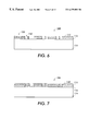
- FIG. 1 respectively. illustrates an SOI wafer that has been etched to form a membrane using Deep Reactive Ion Etching (DRIE) (upper) or wet anisotropic wet etching (lower);
- DRIE Deep Reactive Ion Etching
- FIG. 1 respectively. illustrates an SOI wafer that has been etched to form a membrane using Deep Reactive Ion Etching (DRIE) (upper) or wet anisotropic wet etching (lower);
- DRIE Deep Reactive Ion Etching
- lower wet anisotropic wet etching
- FIGS. 4-17 illustrate process steps to form a MEMS device such as illustrated in FIG. 3 .
- Device 200 includes movable optical elements constructed from single crystal silicon overlaying an insulator such as a diffraction grating 202 , a mirror 204 , and a Fresnel lens 206 .
- Active electronic elements can also be defined in the single crystal is silicon layer, including flip chip bonded light producing laser diodes 201 , light detecting photodiodes 203 , or conventional CMOS logic circuitry 205 .
- Bulk modifications required for packaging or mounting of the substrate are also possible, such as illustrated by etched cavity 208 , and added polysilicon layers can be used for mechanical elements such as hinges 209 .
- FIGS. 4-17 illustrate manufacture of a device such as discussed in connection with FIG. 3, substantially using the foregoing microstructure process steps 1 - 72 .
- a bonded SOI wafer 100 includes a thin silicon crystal layer 112 , and a thick crystal silicon handle wafer layer 114 . Between these two layers 112 and 114 there is an oxide layer 116 that integrally bonds the silicon crystal layer 112 and handle wafer layer 114 .
Abstract
Description
| Step | Process | Specification |
| 1 | Photolithography | a) bake 110 degree C., 15 min |
| Mask #1: Dimple | b) HMDS, 5.OK, 30 sec | |
| c) AZ1813, 4.OK, 30 SEC, 1.3 um | ||
| d) softbake 90 C., 30 min | ||
| e) expose, 5.0 mW/cm2, 12 sec | ||
| f) develop MF 319, 1.1 min | ||
| g) rinse, DI water, 4 min | ||
| h) spin dry | ||
| i) hardbake 110 degree C., 30 min | ||
| 2 | Etch Crystal Silicon | Reactive Ion Etch |
| SF6 + O2 | ||
| 3 | Strip Photoresist | Hot PRS2000, 20 min |
| rinse DI water, 5 min | ||
| spin, dry | ||
| 4 | Photolithography | a) bake 110 degree C., 15 min |
| Mask #2, CRY1 | b) HMDS, 5.OK, 30 sec | |
| c) AZ1813, 4.OK, 30 SEC., 1.3 um | ||
| d) softbake 90 C., 30 min | ||
| e) expose, 5.O mW/cm2, 12 sec | ||
| f) develop MF 319, 1.1 min | ||
| g) rinse, DI water, 4 min | ||
| h) spin dry | ||
| i) hardbake 110 degree C., 30 min | ||
| 5 | Etch Crystal Silicon | STS silicon etch |
| 6 | Etch Oxide under Si | RIE:CF4 + CHF3, target etch rate:250 |
| A/min | ||
| 7 | Strip Photoresist | Hot PRS2000, 20 min |
| rinse DI water, 5 min | ||
| spin, dry | ||
| 8 | Sacrificial Oxide | LPCVD PSG, 1.5 um |
| Deposition | ||
| 9 | Photolithography | a) bake 110 degree C., 15 min |
| Mask #3, Anchor 1 | b) HMDS, 5.OK, 30 sec | |
| (Connect POLY1 to | c) AZ1827, 4.OK, 30 SEC., 2.7 um | |
| CRY1 or Substrate) | d) softbake 90 C., 30 min | |
| e) expose, 5.0 mW/cm2, 12 sec | ||
| f) develop MF 319, 1.1 min | ||
| g) rinse, DI water, 4 min | ||
| h) spin dry | ||
| i) hardbake 110 degree C., 30 min | ||
| 10 | Oxide Etch | Reactive Ion Etch |
| CF4 + CHF3 | ||
| Strip Photoresist | ||
| 11 | Polysilicon Deposition | LPCVD, 2.0 um |
| 12 | PSG Deposition | LPCVD, PSG, 0.3 um |
| 13 | Annealing | 1100 degree C., 60 min |
| 14 | Photolithography | a) bake 110 degree C., 15 min |
| Mask #4, POLY1 | b) HMDS, 5.OK, 30 sec | |
| (Connect POLY1 to | c) AZ1827, 4.OK, 30 SEC., 2.7 um | |
| CRY1 or Substrate | d) softbake 90 C., 30 min | |
| e) expose, 5.0 mW/cm2, 12 sec | ||
| f) develop MF 319, 1.1 min | ||
| g) rinse, DI water, 4 min | ||
| h) spin dry | ||
| i) hardbake 110 degree C., 30 min | ||
| 15 | Oxide Etch | CF4 + CHF3 |
| 16 | Polysilicon Etch | SF6 + O2 |
| 17 | Strip Photoresist | Hot PRS2000, 20 |
| rinse DI water, 5 min | ||
| spin, dry | ||
| 18 | Photolithography | a) bake 110 degree C., 15 min |
| Mask #5, P-Well | b) HMDS, 5.OK, 30 sec | |
| c) AZ1813, 4.OK, 30 SEC., 2.7 um | ||
| d) softbake 90 C., 30 min | ||
| e) expose, 5.0 mW/cm2, 12 sec | ||
| f) develop MF 319, 1.1 min | ||
| g) rinse, DI water, 4 min | ||
| h) spin dry | ||
| i) hardbake 110 degree C., 30 min | ||
| 19 | Implant Well | 2.5E13, 400 KeV, Boron |
| 20 | Strip Photoresist | Hot PRS2000, 20 min |
| rinse DI water, 5 min | ||
| spin, dry | ||
| 21 | Prefurnace Clean | RCA Clean |
| 22 | Pad Oxide | DWDITCA, 900 C., 500A |
| 23 | Nitride Deposition | LPCVD nitride, 1200A |
| 24 | Mask #6, Active | a) bake 110 degree C., 15 min |
| b) HMDS, 5.OK, 30 sec | ||
| c) AZ1813, 4.OK, 30 SEC., 2.7 um | ||
| d) softbake 90 C., 30 min | ||
| e) expose, 5.0 mW/cm2, 12 sec | ||
| f) develop MF 319, 1.1 min | ||
| g) rinse, DI water, 4 min | ||
| h) spin dry | ||
| i) hardbake 110 degree C., 30 min | ||
| 25 | Etch Nitride | RIE: CF4 + O2 |
| 26 | Hardbake Photoresist | |
| 27 | Photolithography | a) bake 110 degree C., 15 min |
| Mask #7, P-Field | b) HMDS, 5.OK, 30 sec | |
| c) AZ1813, 4.OK, 30 SEC., 2.7 um | ||
| d) softbake 90 C., 30 min | ||
| e) expose, 5.0 mW/cm2, 12 sec | ||
| f) develop MF 319, 1.1 min | ||
| g) rinse, DI water, 4 min | ||
| h) spin dry | ||
| i) hardbake 110 degree C., 30 min | ||
| 28 | P-Field Implant | Boron, 5E13, 55KeV |
| 29 | Strip Photoresist | Standard Strip |
| 30 | Prefurnace Clean | |
| 31 | Field Oxidation | DWD/TCAm 1000 C., 9000A |
| 32 | Remove Oxide on | BHF, 30 sec, rinse in DI |
| Nitride | Water, 4 min | |
| 33 | Strip Nitride | phosphoric acid, 180 degree C. |
| 34 | Etch pad Oxide | BHF, 30 sec, rinse in DI |
| water, 4 min | ||
| 35 | Prefurnace Clean | RCA Clean |
| 36 | Grow Sacrificial Oxide | DWDFTCA, 1000 C., 500A |
| 37 | Threshold Implant | Boron, 6.5E11, 35 KeV |
| 38 | Strip Oxide | BHF, 30 sec, rinse in DI Hydrophobic |
| 39 | Prefurnace Clean | RCA Clean |
| 40 | Grow Gate Oxide | DA1, 1000 C., 400A |
| 41 | Deposit Gate Poly | LPCVD, Poly 5000A |
| 42 | Dope Poly | B3, Phosdep2 <20 ohm/square |
| 43 | Photolithography | a) bake 110 degree C., 15 min |
| ask #8, Gate | b) HMDS, 5.OK, 30 sec | |
| c) AZ1813, 4.OK, 30 SEC., 2.7 um | ||
| d) softbake 90 C., 30 min | ||
| e) expose, 5.0 mW/cm2, 12 sec | ||
| f) develop MF 319, 1.1 min | ||
| g) rinse, DI water, 4 min | ||
| h) spin dry | ||
| i) hardbake 110 degree C., 30 min | ||
| 44 | Etch Poly | RIE: SF6 + O2 |
| 45 | Strip Photoresist | Standard Strip |
| 46 | Prefurnace Clean | RCA Clean |
| 47 | Grow Capacitor Oxide | DA1, 1000 C., 750A |
| 48 | Deposit Poly | LPCVD Poly, 5500A |
| 49 | Dope Poly | B3, Phosphorus <20 ohm/square |
| 50 | Mask #9, Poly2 | a) bake 110 degree C., 15 min |
| b) HMDS, 5.OK, 30 sec | ||
| c) AZ1813, 4.OK, 30 SEC., 2.7 um | ||
| d) softbake 90 C., 30 min | ||
| e) expose, 5.0 mW/cm2, 12 sec | ||
| f) develop MF 319, 1.1 min | ||
| g) rinse, DI water, 4 min | ||
| h) spin dry | ||
| i) hardbake 110 degree C., 30 min | ||
| 51 | Poly2 Etch | RIE, SF6 + O2 |
| 52 | Strip Photoresist | PRS 2000, 20 min |
| 53 | Prefurnace Clean | RCA Clean |
| 54 | Reoxidation | B4, DWDA1, 800 C., 1200A |
| 55 | Mask #10, P + Implant | a) bake 110 degree C., 15 min |
| b) HMDS, 5.OK, 30 sec | ||
| c) AZ1813, 4.OK, 30 SEC., 2.7 um | ||
| d) softbake 90 C., 30 min | ||
| e) expose, 5.0 mW/cm2 , 12 sec | ||
| f) develop MF 319, 1.1 min | ||
| g) rinse, DI water, 4 min | ||
| h) spin dry | ||
| i) hardbake 110 degree C., 30 min | ||
| 56 | P + Implant | 7E15, 40 KeV, Boron |
| 57 | Strip Photoresist | Hot PRS2000, 20 min |
| 58 | Photolithography | a) bake 110 degree C., 15 min |
| Mask #10, P + Implant | b) HMDS, 5.OK, 30 sec | |
| (Image Reversal) | c) AZ5214, 4.OK, 30 SEC., 2.7 um | |
| d) softbake 90 C., 30 min | ||
| e) expose, 5.0 mW/cm2, 12 sec | ||
| f) Soft bake, 100 C., 30 min | ||
| g) Flood Expose, 42 sec | ||
| h) Develop AZ312, 1.1 min | ||
| i) Rinse, DI water, 4 min | ||
| j) spin dry | ||
| k) postbake 110 C., 30 min | ||
| 59 | N + Implant | Phosphorus, 8E15, 70 KeV |
| 60 | Strip Photoresist | Hot PRS2000, 20 min |
| 61 | Prefurnace Clean | RCA Clean |
| 62 | Deposit CVD Oxide | LTO 0.5 um |
| 63 | Mask #11, CONTACTS | a) bake 110 degree C., 15 min |
| b) HMDS, 5.OK, 30 sec | ||
| c) AZ1813, 4.OK, 30 SEC., 2.7 um | ||
| d) softbake 90 C., 30 min | ||
| e) expose, 5.0 mW/cm2, 12 sec | ||
| f) develop MF 319, 1.1 min | ||
| g) rinse, DI water, 4 min | ||
| h) spin dry | ||
| i) hardbake 110 degree C., 30 min | ||
| 64 | Etch Contacts | RIE, CF$ + CHF3 |
| 65 | Strip Photoresist | Hot PRS2000, 20 min |
| 66 | Mask #12, Metal | a) bake 110 degree C., 15 min |
| b) HMDS, 5.OK, 30 sec | ||
| c) AZ1813, 4.OK, 30 SEC., 2.7 um | ||
| d) softbake 90 C., 30 min | ||
| e) expose, 5.0 mW/cm2, 12 sec | ||
| f) develop MF 319, 1.1 min | ||
| g) rinse, DI water, 4 min | ||
| h) spin dry | ||
| i) hardbake 110 degree C., 30 min | ||
| 67 | Sputter Cr/Au | Cr/Au: 300A/3000A |
| 68 | Lift-off | Hot 1112A |
| 69 | Clean Water | ACE/IPA |
| 70 | Eutectic bonding | Bond a LED/Laser Diode to the |
| Substrate | ||
| 71 | Water Dicing | |
| 72 | Microstructure Release | HF: water = 1:1 |
| Rinse DI water | ||
Claims (15)
Priority Applications (1)
| Application Number | Priority Date | Filing Date | Title |
|---|---|---|---|
| US09/468,141 US6379989B1 (en) | 1998-12-23 | 1999-12-21 | Process for manufacture of microoptomechanical structures |
Applications Claiming Priority (2)
| Application Number | Priority Date | Filing Date | Title |
|---|---|---|---|
| US11377798P | 1998-12-23 | 1998-12-23 | |
| US09/468,141 US6379989B1 (en) | 1998-12-23 | 1999-12-21 | Process for manufacture of microoptomechanical structures |
Publications (1)
| Publication Number | Publication Date |
|---|---|
| US6379989B1 true US6379989B1 (en) | 2002-04-30 |
Family
ID=26811459
Family Applications (1)
| Application Number | Title | Priority Date | Filing Date |
|---|---|---|---|
| US09/468,141 Expired - Lifetime US6379989B1 (en) | 1998-12-23 | 1999-12-21 | Process for manufacture of microoptomechanical structures |
Country Status (1)
| Country | Link |
|---|---|
| US (1) | US6379989B1 (en) |
Cited By (34)
| Publication number | Priority date | Publication date | Assignee | Title |
|---|---|---|---|---|
| US20020118850A1 (en) * | 2000-08-02 | 2002-08-29 | Yeh Jer-Liang (Andrew) | Micromachine directional microphone and associated method |
| US6506620B1 (en) * | 2000-11-27 | 2003-01-14 | Microscan Systems Incorporated | Process for manufacturing micromechanical and microoptomechanical structures with backside metalization |
| US20030044106A1 (en) * | 2001-07-24 | 2003-03-06 | Chuang-Chia Lin | Mems element having perpendicular portion formed from substrate |
| US6583031B2 (en) * | 2001-07-25 | 2003-06-24 | Onix Microsystems, Inc. | Method of making a MEMS element having perpendicular portion formed from substrate |
| US20030118076A1 (en) * | 2001-09-10 | 2003-06-26 | Perkinelmer Optoelectronics Gmbh | Sensor for a contact-free temperature measurement |
| US6661070B2 (en) | 2000-11-27 | 2003-12-09 | Microscan Systems, Inc. | Micromechanical and microoptomechanical structures with single crystal silicon exposure step |
| US6677225B1 (en) * | 2000-07-14 | 2004-01-13 | Zyvex Corporation | System and method for constraining totally released microcomponents |
| US20040155571A1 (en) * | 2002-03-28 | 2004-08-12 | Lothar Hitzschke | Discharge lamp for dielectrically impeded discharges having a corrugated cover plate structure |
| US6790698B2 (en) * | 2000-10-19 | 2004-09-14 | Axsun Technologies, Inc. | Process for integrating dielectric optical coatings into micro-electromechanical devices |
| US20040240034A1 (en) * | 2001-11-30 | 2004-12-02 | Scharf Bruce R. | Diffraction compensation using a patterned reflector |
| US20050019974A1 (en) * | 2003-07-25 | 2005-01-27 | Markus Lutz | Anchors for microelectromechanical systems having an SOI substrate, and method of fabricating same |
| US20050031288A1 (en) * | 2003-08-05 | 2005-02-10 | Xerox Corporation. | Thermal actuator and an optical waveguide switch including the same |
| US20050031253A1 (en) * | 2003-08-05 | 2005-02-10 | Xerox Corporation | Thermal actuator with offset beam segment neutral axes and an optical waveguide switch including the same |
| US20050031252A1 (en) * | 2003-08-05 | 2005-02-10 | Xerox Corporation | Thermal actuator and an optical waveguide switch including the same |
| US20050124135A1 (en) * | 2003-11-25 | 2005-06-09 | Farrokh Ayazi | Methods of forming oxide masks with submicron openings and microstructures formed thereby |
| US20050177580A1 (en) * | 2004-02-11 | 2005-08-11 | Hilbert David M. | System and method for customized document selection |
| US20050188026A1 (en) * | 2004-02-11 | 2005-08-25 | Hilbert David M. | Email distribution system and method |
| US20060033594A1 (en) * | 2004-03-04 | 2006-02-16 | Markus Lutz | Temperature controlled MEMS resonator and method for controlling resonator frequency |
| US20060110101A1 (en) * | 2004-11-23 | 2006-05-25 | Xerox Corporation | Microfabrication process for control of waveguide gap size |
| US20060119793A1 (en) * | 2004-12-03 | 2006-06-08 | Hillis W D | Temporal vision modification |
| US20060119794A1 (en) * | 2004-12-03 | 2006-06-08 | Hillis W D | Vision modification with reflected image |
| US20060122530A1 (en) * | 2004-12-03 | 2006-06-08 | Goodall Eleanor V | Adjustable lens system with neural-based control |
| US20060122531A1 (en) * | 2004-12-03 | 2006-06-08 | Goodall Eleanor V | Method and system for adaptive vision modification |
| US20060146281A1 (en) * | 2004-12-03 | 2006-07-06 | Goodall Eleanor V | Method and system for vision enhancement |
| US20070010757A1 (en) * | 2004-12-03 | 2007-01-11 | Searete Llc | Method and system for adaptive vision modification |
| US20070019279A1 (en) * | 2004-12-03 | 2007-01-25 | Searete Llc, A Limited Liability Corporation Of The State Of Delaware | Adjustable lens system with neural-based control |
| US20070019157A1 (en) * | 2004-12-03 | 2007-01-25 | Searete Llc, A Limited Liability Corporation Of The State Of Delaware | Vision modification with reflected image |
| US20070019272A1 (en) * | 2004-12-03 | 2007-01-25 | Searete Llc, A Limited Liability Corporation Of The State Of Delaware | Vision modification with reflected image |
| US20070028931A1 (en) * | 2004-12-03 | 2007-02-08 | Searete Llc, A Limited Liability Corporation Of The State Of Delaware | Temporal vision modification |
| US20080137031A1 (en) * | 2004-12-03 | 2008-06-12 | Searete Llc, A Limited Liability Corporation Of The State Of Delaware | Vision modification with reflected image |
| US20090195751A1 (en) * | 2004-12-03 | 2009-08-06 | Searete Llc | Vision modification with reflected image |
| US20090275162A1 (en) * | 2008-03-18 | 2009-11-05 | Solid-State Research | Cmos-compatible bulk-micromachining process for single-crystal mems/nems devices |
| US8869390B2 (en) | 2007-10-01 | 2014-10-28 | Innurvation, Inc. | System and method for manufacturing a swallowable sensor device |
| US9155483B2 (en) | 2004-12-03 | 2015-10-13 | The Invention Science Fund I, Llc | Vision modification with reflected image |
Citations (11)
| Publication number | Priority date | Publication date | Assignee | Title |
|---|---|---|---|---|
| DE4318466A1 (en) * | 1993-06-03 | 1994-12-08 | Bosch Gmbh Robert | Micromechanical sensor and method for its production |
| US5484073A (en) * | 1994-03-28 | 1996-01-16 | I/O Sensors, Inc. | Method for fabricating suspension members for micromachined sensors |
| US5569355A (en) * | 1995-01-11 | 1996-10-29 | Center For Advanced Fiberoptic Applications | Method for fabrication of microchannel electron multipliers |
| US5589083A (en) * | 1993-12-11 | 1996-12-31 | Electronics And Telecommunications Research Institute | Method of manufacturing microstructure by the anisotropic etching and bonding of substrates |
| DE19603829A1 (en) * | 1996-02-02 | 1997-08-07 | Daimler Benz Ag | Silicon@ based micromechanical structure manufacturing method |
| US5853960A (en) * | 1998-03-18 | 1998-12-29 | Trw Inc. | Method for producing a micro optical semiconductor lens |
| US5962081A (en) * | 1995-06-21 | 1999-10-05 | Pharmacia Biotech Ab | Method for the manufacture of a membrane-containing microstructure |
| US6074890A (en) * | 1998-01-08 | 2000-06-13 | Rockwell Science Center, Llc | Method of fabricating suspended single crystal silicon micro electro mechanical system (MEMS) devices |
| US6084257A (en) * | 1995-05-24 | 2000-07-04 | Lucas Novasensor | Single crystal silicon sensor with high aspect ratio and curvilinear structures |
| US6117344A (en) * | 1998-03-20 | 2000-09-12 | Borealis Technical Limited | Method for manufacturing low work function surfaces |
| US6238581B1 (en) * | 1998-12-18 | 2001-05-29 | Eastman Kodak Company | Process for manufacturing an electro-mechanical grating device |
-
1999
- 1999-12-21 US US09/468,141 patent/US6379989B1/en not_active Expired - Lifetime
Patent Citations (11)
| Publication number | Priority date | Publication date | Assignee | Title |
|---|---|---|---|---|
| DE4318466A1 (en) * | 1993-06-03 | 1994-12-08 | Bosch Gmbh Robert | Micromechanical sensor and method for its production |
| US5589083A (en) * | 1993-12-11 | 1996-12-31 | Electronics And Telecommunications Research Institute | Method of manufacturing microstructure by the anisotropic etching and bonding of substrates |
| US5484073A (en) * | 1994-03-28 | 1996-01-16 | I/O Sensors, Inc. | Method for fabricating suspension members for micromachined sensors |
| US5569355A (en) * | 1995-01-11 | 1996-10-29 | Center For Advanced Fiberoptic Applications | Method for fabrication of microchannel electron multipliers |
| US6084257A (en) * | 1995-05-24 | 2000-07-04 | Lucas Novasensor | Single crystal silicon sensor with high aspect ratio and curvilinear structures |
| US5962081A (en) * | 1995-06-21 | 1999-10-05 | Pharmacia Biotech Ab | Method for the manufacture of a membrane-containing microstructure |
| DE19603829A1 (en) * | 1996-02-02 | 1997-08-07 | Daimler Benz Ag | Silicon@ based micromechanical structure manufacturing method |
| US6074890A (en) * | 1998-01-08 | 2000-06-13 | Rockwell Science Center, Llc | Method of fabricating suspended single crystal silicon micro electro mechanical system (MEMS) devices |
| US5853960A (en) * | 1998-03-18 | 1998-12-29 | Trw Inc. | Method for producing a micro optical semiconductor lens |
| US6117344A (en) * | 1998-03-20 | 2000-09-12 | Borealis Technical Limited | Method for manufacturing low work function surfaces |
| US6238581B1 (en) * | 1998-12-18 | 2001-05-29 | Eastman Kodak Company | Process for manufacturing an electro-mechanical grating device |
Non-Patent Citations (4)
| Title |
|---|
| Advanced Silicon Etching Using High Density Plasmas, J. K. Bhardwaj and H. Ashraf, SPIE vol. 2639. |
| Microfabricated Hinges, K. S. J. Pister, M. W. Judy, S. R. Burgett and R. S. Fearing, Mar. 1992. |
| Micro-Machined Three-Dimensional Micro-Optics for Integrated Free-Space Optical System, L. Y. Lin, S. S. Lee and K. S. J. Pister, 1994. |
| Surface Micromachining for Microsensors and Microactuators, Roger T. Howe, J. Vac. Sci. Technol. B6(6), Nov./Dec. 1999. |
Cited By (56)
| Publication number | Priority date | Publication date | Assignee | Title |
|---|---|---|---|---|
| US6677225B1 (en) * | 2000-07-14 | 2004-01-13 | Zyvex Corporation | System and method for constraining totally released microcomponents |
| US20020118850A1 (en) * | 2000-08-02 | 2002-08-29 | Yeh Jer-Liang (Andrew) | Micromachine directional microphone and associated method |
| US6790698B2 (en) * | 2000-10-19 | 2004-09-14 | Axsun Technologies, Inc. | Process for integrating dielectric optical coatings into micro-electromechanical devices |
| US6506620B1 (en) * | 2000-11-27 | 2003-01-14 | Microscan Systems Incorporated | Process for manufacturing micromechanical and microoptomechanical structures with backside metalization |
| US6661070B2 (en) | 2000-11-27 | 2003-12-09 | Microscan Systems, Inc. | Micromechanical and microoptomechanical structures with single crystal silicon exposure step |
| US20030044106A1 (en) * | 2001-07-24 | 2003-03-06 | Chuang-Chia Lin | Mems element having perpendicular portion formed from substrate |
| US6813412B2 (en) | 2001-07-24 | 2004-11-02 | Michael J. Daneman | Mems element having perpendicular portion formed from substrate |
| US6583031B2 (en) * | 2001-07-25 | 2003-06-24 | Onix Microsystems, Inc. | Method of making a MEMS element having perpendicular portion formed from substrate |
| US20030118076A1 (en) * | 2001-09-10 | 2003-06-26 | Perkinelmer Optoelectronics Gmbh | Sensor for a contact-free temperature measurement |
| US20040240034A1 (en) * | 2001-11-30 | 2004-12-02 | Scharf Bruce R. | Diffraction compensation using a patterned reflector |
| US20040155571A1 (en) * | 2002-03-28 | 2004-08-12 | Lothar Hitzschke | Discharge lamp for dielectrically impeded discharges having a corrugated cover plate structure |
| US20050253209A1 (en) * | 2003-07-25 | 2005-11-17 | Markus Lutz | Anchors for microelectromechanical systems having an SOI substrate, and method of fabricating same |
| US20050019974A1 (en) * | 2003-07-25 | 2005-01-27 | Markus Lutz | Anchors for microelectromechanical systems having an SOI substrate, and method of fabricating same |
| US6983088B2 (en) | 2003-08-05 | 2006-01-03 | Xerox Corporation | Thermal actuator and an optical waveguide switch including the same |
| US20050031252A1 (en) * | 2003-08-05 | 2005-02-10 | Xerox Corporation | Thermal actuator and an optical waveguide switch including the same |
| US20050031253A1 (en) * | 2003-08-05 | 2005-02-10 | Xerox Corporation | Thermal actuator with offset beam segment neutral axes and an optical waveguide switch including the same |
| US20050031288A1 (en) * | 2003-08-05 | 2005-02-10 | Xerox Corporation. | Thermal actuator and an optical waveguide switch including the same |
| US6985651B2 (en) | 2003-08-05 | 2006-01-10 | Xerox Corporation | Thermal actuator with offset beam segment neutral axes and an optical waveguide switch including the same |
| US6985650B2 (en) | 2003-08-05 | 2006-01-10 | Xerox Corporation | Thermal actuator and an optical waveguide switch including the same |
| US7056757B2 (en) * | 2003-11-25 | 2006-06-06 | Georgia Tech Research Corporation | Methods of forming oxide masks with submicron openings and microstructures formed thereby |
| US20050124135A1 (en) * | 2003-11-25 | 2005-06-09 | Farrokh Ayazi | Methods of forming oxide masks with submicron openings and microstructures formed thereby |
| US20050177580A1 (en) * | 2004-02-11 | 2005-08-11 | Hilbert David M. | System and method for customized document selection |
| US20050188026A1 (en) * | 2004-02-11 | 2005-08-25 | Hilbert David M. | Email distribution system and method |
| US7395267B2 (en) | 2004-02-11 | 2008-07-01 | Fuji Xerox Co., Ltd. | System and method for customized document selection |
| US20060033594A1 (en) * | 2004-03-04 | 2006-02-16 | Markus Lutz | Temperature controlled MEMS resonator and method for controlling resonator frequency |
| US20060110101A1 (en) * | 2004-11-23 | 2006-05-25 | Xerox Corporation | Microfabrication process for control of waveguide gap size |
| US7162112B2 (en) | 2004-11-23 | 2007-01-09 | Xerox Corporation | Microfabrication process for control of waveguide gap size |
| US20060122531A1 (en) * | 2004-12-03 | 2006-06-08 | Goodall Eleanor V | Method and system for adaptive vision modification |
| US20100103373A1 (en) * | 2004-12-03 | 2010-04-29 | Searete Llc | Vision modification with reflected image |
| US20060146281A1 (en) * | 2004-12-03 | 2006-07-06 | Goodall Eleanor V | Method and system for vision enhancement |
| US20060119794A1 (en) * | 2004-12-03 | 2006-06-08 | Hillis W D | Vision modification with reflected image |
| US20070010757A1 (en) * | 2004-12-03 | 2007-01-11 | Searete Llc | Method and system for adaptive vision modification |
| US20070019279A1 (en) * | 2004-12-03 | 2007-01-25 | Searete Llc, A Limited Liability Corporation Of The State Of Delaware | Adjustable lens system with neural-based control |
| US20070019157A1 (en) * | 2004-12-03 | 2007-01-25 | Searete Llc, A Limited Liability Corporation Of The State Of Delaware | Vision modification with reflected image |
| US20070019272A1 (en) * | 2004-12-03 | 2007-01-25 | Searete Llc, A Limited Liability Corporation Of The State Of Delaware | Vision modification with reflected image |
| US20070028931A1 (en) * | 2004-12-03 | 2007-02-08 | Searete Llc, A Limited Liability Corporation Of The State Of Delaware | Temporal vision modification |
| US20080137031A1 (en) * | 2004-12-03 | 2008-06-12 | Searete Llc, A Limited Liability Corporation Of The State Of Delaware | Vision modification with reflected image |
| US20060119793A1 (en) * | 2004-12-03 | 2006-06-08 | Hillis W D | Temporal vision modification |
| US20080161673A1 (en) * | 2004-12-03 | 2008-07-03 | Searete Llc. | Method and system for adaptive vision modification |
| US20090195751A1 (en) * | 2004-12-03 | 2009-08-06 | Searete Llc | Vision modification with reflected image |
| US10409088B2 (en) | 2004-12-03 | 2019-09-10 | Gearbox, Llc | Adjustable contact lens system |
| US7656569B2 (en) | 2004-12-03 | 2010-02-02 | Searete Llc | Vision modification with reflected image |
| US20060122530A1 (en) * | 2004-12-03 | 2006-06-08 | Goodall Eleanor V | Adjustable lens system with neural-based control |
| US9459470B2 (en) | 2004-12-03 | 2016-10-04 | Gearbox, Llc | Vision modification with reflected image |
| US20100177279A1 (en) * | 2004-12-03 | 2010-07-15 | Searete Llc | Vision modification with reflected image |
| US7931373B2 (en) | 2004-12-03 | 2011-04-26 | The Invention Science Fund I, Llc | Vision modification with reflected image |
| US8104892B2 (en) | 2004-12-03 | 2012-01-31 | The Invention Science Fund I, Llc | Vision modification with reflected image |
| US8109632B2 (en) | 2004-12-03 | 2012-02-07 | The Invention Science Fund I, Llc | Vision modification with reflected image |
| US8244342B2 (en) | 2004-12-03 | 2012-08-14 | The Invention Science Fund I, Llc | Method and system for adaptive vision modification |
| US8282212B2 (en) | 2004-12-03 | 2012-10-09 | The Invention Science Fund I, Llc | Vision modification with reflected image |
| US8562540B2 (en) | 2004-12-03 | 2013-10-22 | The Invention Science Fund I, Llc | Method and system for adaptive vision modification |
| US9155483B2 (en) | 2004-12-03 | 2015-10-13 | The Invention Science Fund I, Llc | Vision modification with reflected image |
| US8869390B2 (en) | 2007-10-01 | 2014-10-28 | Innurvation, Inc. | System and method for manufacturing a swallowable sensor device |
| US9730336B2 (en) | 2007-10-01 | 2017-08-08 | Innurvation, Inc. | System for manufacturing a swallowable sensor device |
| US7749789B2 (en) * | 2008-03-18 | 2010-07-06 | Solid-State Research, Inc. | CMOS-compatible bulk-micromachining process for single-crystal MEMS/NEMS devices |
| US20090275162A1 (en) * | 2008-03-18 | 2009-11-05 | Solid-State Research | Cmos-compatible bulk-micromachining process for single-crystal mems/nems devices |
Similar Documents
| Publication | Publication Date | Title |
|---|---|---|
| US6379989B1 (en) | Process for manufacture of microoptomechanical structures | |
| US6362512B1 (en) | Microelectromechanical structures defined from silicon on insulator wafers | |
| US6506620B1 (en) | Process for manufacturing micromechanical and microoptomechanical structures with backside metalization | |
| US6479315B1 (en) | Process for manufacturing micromechanical and microoptomechanical structures with single crystal silicon exposure step | |
| US7486430B2 (en) | Single-crystal-silicon 3D micromirror | |
| US7083997B2 (en) | Bonded wafer optical MEMS process | |
| JP6040253B2 (en) | Integrated monolithic optical bench including 3D curved optical element and method for manufacturing the same | |
| US20020118850A1 (en) | Micromachine directional microphone and associated method | |
| KR100373739B1 (en) | Method for Fabrication of Electrostatic Vertical Actuators Using One Single-crystalline Silicon Wafer | |
| EP1741669B1 (en) | Hidden hinge MEMS device | |
| Wu et al. | Design and fabrication of MEMS devices using the integration of MUMPs, trench-refilled molding, DRIE and bulk silicon etching processes | |
| KR100817813B1 (en) | A method for fabricating a micro structures with multi differential gap on silicon substrate | |
| US6479311B1 (en) | Process for manufacturing micromechanical and microoptomechanical structures with pre-applied patterning | |
| Lapisa et al. | CMOS-integrable piston-type micro-mirror array for adaptive optics made of mono-crystalline silicon using 3-D integration | |
| US6525352B1 (en) | Method to reduce release time of micromachined devices | |
| Hofmann et al. | Monolithic three-dimensional single-crystal silicon microelectromechanical systems | |
| US6858459B2 (en) | Method of fabricating micro-mirror switching device | |
| Wu et al. | Design and fabrication of MEMS devices using the integration of MUMPs, trench-refilled molding, DRIE and bulk silicon etching process | |
| JP3871118B2 (en) | Microdevice manufacturing method | |
| GB2375185A (en) | Thick wafer for MEMS fabrication | |
| Lutzenberger et al. | Large area molded silicon nitride micro mirrors | |
| CN111629991A (en) | Interposer substrate, MEMS device and corresponding manufacturing method | |
| Wu et al. | Integrating the SOI and poly-Si surface structures in a monolithic process for optical devices platform | |
| Jung et al. | Large-area high-reflectivity broadband monolithic silicon photonic crystal mirror MEMS scanner | |
| Singh et al. | Micromirror Switching Device Fabrication for Optical Communication Network Applications |
Legal Events
| Date | Code | Title | Description |
|---|---|---|---|
| AS | Assignment |
Owner name: XEROX CORPORATION, CONNECTICUT Free format text: ASSIGNMENT OF ASSIGNORS INTEREST;ASSIGNORS:KUBBY, JOEL A.;CHEN, JINGKUANG;TRAN, ALEX T.;REEL/FRAME:010906/0257;SIGNING DATES FROM 20000307 TO 20000530 |
|
| STCF | Information on status: patent grant |
Free format text: PATENTED CASE |
|
| AS | Assignment |
Owner name: BANK ONE, NA, AS ADMINISTRATIVE AGENT, ILLINOIS Free format text: SECURITY INTEREST;ASSIGNOR:XEROX CORPORATION;REEL/FRAME:013153/0001 Effective date: 20020621 |
|
| AS | Assignment |
Owner name: JPMORGAN CHASE BANK, AS COLLATERAL AGENT, TEXAS Free format text: SECURITY AGREEMENT;ASSIGNOR:XEROX CORPORATION;REEL/FRAME:015134/0476 Effective date: 20030625 Owner name: JPMORGAN CHASE BANK, AS COLLATERAL AGENT,TEXAS Free format text: SECURITY AGREEMENT;ASSIGNOR:XEROX CORPORATION;REEL/FRAME:015134/0476 Effective date: 20030625 |
|
| FPAY | Fee payment |
Year of fee payment: 4 |
|
| FPAY | Fee payment |
Year of fee payment: 8 |
|
| FPAY | Fee payment |
Year of fee payment: 12 |
|
| AS | Assignment |
Owner name: XEROX CORPORATION, CONNECTICUT Free format text: RELEASE BY SECURED PARTY;ASSIGNOR:JPMORGAN CHASE BANK, N.A. AS SUCCESSOR-IN-INTEREST ADMINISTRATIVE AGENT AND COLLATERAL AGENT TO JPMORGAN CHASE BANK;REEL/FRAME:066728/0193 Effective date: 20220822 |