US6452276B1 - Ultra thin, single phase, diffusion barrier for metal conductors - Google Patents

Ultra thin, single phase, diffusion barrier for metal conductors Download PDF

Info

Publication number
US6452276B1
US6452276B1 US09/070,394 US7039498A US6452276B1 US 6452276 B1 US6452276 B1 US 6452276B1 US 7039498 A US7039498 A US 7039498A US 6452276 B1 US6452276 B1 US 6452276B1
Authority
US
United States
Prior art keywords
layer
alpha
barrier layer
dielectric material
dielectric
Prior art date
Legal status (The legal status is an assumption and is not a legal conclusion. Google has not performed a legal analysis and makes no representation as to the accuracy of the status listed.)
Expired - Fee Related
Application number
US09/070,394
Inventor
Stephan A. Cohen
Fenton R. McFeely
Cevdet I. Noyan
Kenneth P. Rodbell
John J. Yurkas
Robert Rosenberg
Current Assignee (The listed assignees may be inaccurate. Google has not performed a legal analysis and makes no representation or warranty as to the accuracy of the list.)
GlobalFoundries Inc
Original Assignee
International Business Machines Corp
Priority date (The priority date is an assumption and is not a legal conclusion. Google has not performed a legal analysis and makes no representation as to the accuracy of the date listed.)
Filing date
Publication date
Priority to US09/070,394 priority Critical patent/US6452276B1/en
Application filed by International Business Machines Corp filed Critical International Business Machines Corp
Assigned to INTERNATIONAL BUSINESS MACHINES CORPORATION reassignment INTERNATIONAL BUSINESS MACHINES CORPORATION ASSIGNMENT OF ASSIGNORS INTEREST (SEE DOCUMENT FOR DETAILS). Assignors: RODBELL, KENNETH P., ROSENBERG, ROBERT, COHEN, STEPHEN A., YURKAS, JOHN J., MCFEELY, FENTON R., NOYAN, CEVDET I.
Assigned to INTERNATIONAL BUSINESS MACHINES CORPORATION reassignment INTERNATIONAL BUSINESS MACHINES CORPORATION ASSIGNMENT OF ASSIGNORS INTEREST (SEE DOCUMENT FOR DETAILS). Assignors: ROSENBERG, ROBERT, YURKAS, JOHN J., COHEN, STEPHAN A., MCFEELY, FENTON R., NOYAN, CEVDET I., RODBELL, KENNETH P.
Priority to TW088101964A priority patent/TW482826B/en
Priority to KR10-1999-0008451A priority patent/KR100386529B1/en
Priority to CNB991044428A priority patent/CN1134060C/en
Priority to SG9901658A priority patent/SG81271A1/en
Priority to JP11757899A priority patent/JP3177228B2/en
Priority to EP99303340A priority patent/EP0954016A3/en
Priority to US10/188,686 priority patent/US7172968B2/en
Publication of US6452276B1 publication Critical patent/US6452276B1/en
Application granted granted Critical
Assigned to GLOBALFOUNDRIES U.S. 2 LLC reassignment GLOBALFOUNDRIES U.S. 2 LLC ASSIGNMENT OF ASSIGNORS INTEREST (SEE DOCUMENT FOR DETAILS). Assignors: INTERNATIONAL BUSINESS MACHINES CORPORATION
Assigned to GLOBALFOUNDRIES INC. reassignment GLOBALFOUNDRIES INC. ASSIGNMENT OF ASSIGNORS INTEREST (SEE DOCUMENT FOR DETAILS). Assignors: GLOBALFOUNDRIES U.S. 2 LLC, GLOBALFOUNDRIES U.S. INC.
Anticipated expiration legal-status Critical
Expired - Fee Related legal-status Critical Current

Links

Images

Classifications

    • HELECTRICITY
    • H01ELECTRIC ELEMENTS
    • H01LSEMICONDUCTOR DEVICES NOT COVERED BY CLASS H10
    • H01L21/00Processes or apparatus adapted for the manufacture or treatment of semiconductor or solid state devices or of parts thereof
    • H01L21/70Manufacture or treatment of devices consisting of a plurality of solid state components formed in or on a common substrate or of parts thereof; Manufacture of integrated circuit devices or of parts thereof
    • H01L21/71Manufacture of specific parts of devices defined in group H01L21/70
    • H01L21/768Applying interconnections to be used for carrying current between separate components within a device comprising conductors and dielectrics
    • H01L21/76838Applying interconnections to be used for carrying current between separate components within a device comprising conductors and dielectrics characterised by the formation and the after-treatment of the conductors
    • H01L21/76841Barrier, adhesion or liner layers
    • H01L21/7687Thin films associated with contacts of capacitors
    • HELECTRICITY
    • H01ELECTRIC ELEMENTS
    • H01LSEMICONDUCTOR DEVICES NOT COVERED BY CLASS H10
    • H01L21/00Processes or apparatus adapted for the manufacture or treatment of semiconductor or solid state devices or of parts thereof
    • H01L21/70Manufacture or treatment of devices consisting of a plurality of solid state components formed in or on a common substrate or of parts thereof; Manufacture of integrated circuit devices or of parts thereof
    • H01L21/71Manufacture of specific parts of devices defined in group H01L21/70
    • H01L21/768Applying interconnections to be used for carrying current between separate components within a device comprising conductors and dielectrics
    • H01L21/76838Applying interconnections to be used for carrying current between separate components within a device comprising conductors and dielectrics characterised by the formation and the after-treatment of the conductors
    • H01L21/76841Barrier, adhesion or liner layers
    • H01L21/76843Barrier, adhesion or liner layers formed in openings in a dielectric
    • HELECTRICITY
    • H01ELECTRIC ELEMENTS
    • H01LSEMICONDUCTOR DEVICES NOT COVERED BY CLASS H10
    • H01L23/00Details of semiconductor or other solid state devices
    • H01L23/52Arrangements for conducting electric current within the device in operation from one component to another, i.e. interconnections, e.g. wires, lead frames
    • H01L23/522Arrangements for conducting electric current within the device in operation from one component to another, i.e. interconnections, e.g. wires, lead frames including external interconnections consisting of a multilayer structure of conductive and insulating layers inseparably formed on the semiconductor body
    • H01L23/532Arrangements for conducting electric current within the device in operation from one component to another, i.e. interconnections, e.g. wires, lead frames including external interconnections consisting of a multilayer structure of conductive and insulating layers inseparably formed on the semiconductor body characterised by the materials
    • H01L23/53204Conductive materials
    • H01L23/53209Conductive materials based on metals, e.g. alloys, metal silicides
    • H01L23/53214Conductive materials based on metals, e.g. alloys, metal silicides the principal metal being aluminium
    • H01L23/53223Additional layers associated with aluminium layers, e.g. adhesion, barrier, cladding layers
    • HELECTRICITY
    • H01ELECTRIC ELEMENTS
    • H01LSEMICONDUCTOR DEVICES NOT COVERED BY CLASS H10
    • H01L23/00Details of semiconductor or other solid state devices
    • H01L23/52Arrangements for conducting electric current within the device in operation from one component to another, i.e. interconnections, e.g. wires, lead frames
    • H01L23/522Arrangements for conducting electric current within the device in operation from one component to another, i.e. interconnections, e.g. wires, lead frames including external interconnections consisting of a multilayer structure of conductive and insulating layers inseparably formed on the semiconductor body
    • H01L23/532Arrangements for conducting electric current within the device in operation from one component to another, i.e. interconnections, e.g. wires, lead frames including external interconnections consisting of a multilayer structure of conductive and insulating layers inseparably formed on the semiconductor body characterised by the materials
    • H01L23/53204Conductive materials
    • H01L23/53209Conductive materials based on metals, e.g. alloys, metal silicides
    • H01L23/53228Conductive materials based on metals, e.g. alloys, metal silicides the principal metal being copper
    • H01L23/53238Additional layers associated with copper layers, e.g. adhesion, barrier, cladding layers
    • HELECTRICITY
    • H01ELECTRIC ELEMENTS
    • H01LSEMICONDUCTOR DEVICES NOT COVERED BY CLASS H10
    • H01L23/00Details of semiconductor or other solid state devices
    • H01L23/52Arrangements for conducting electric current within the device in operation from one component to another, i.e. interconnections, e.g. wires, lead frames
    • H01L23/522Arrangements for conducting electric current within the device in operation from one component to another, i.e. interconnections, e.g. wires, lead frames including external interconnections consisting of a multilayer structure of conductive and insulating layers inseparably formed on the semiconductor body
    • H01L23/532Arrangements for conducting electric current within the device in operation from one component to another, i.e. interconnections, e.g. wires, lead frames including external interconnections consisting of a multilayer structure of conductive and insulating layers inseparably formed on the semiconductor body characterised by the materials
    • H01L23/5329Insulating materials
    • HELECTRICITY
    • H01ELECTRIC ELEMENTS
    • H01LSEMICONDUCTOR DEVICES NOT COVERED BY CLASS H10
    • H01L2924/00Indexing scheme for arrangements or methods for connecting or disconnecting semiconductor or solid-state bodies as covered by H01L24/00
    • H01L2924/0001Technical content checked by a classifier
    • H01L2924/0002Not covered by any one of groups H01L24/00, H01L24/00 and H01L2224/00

Definitions

  • the present invention relates to interconnect semiconductor structures and, in particular to an alpha-phase W barrier layer that is formed in the trenches or vias of such interconnect structures using a low temperature/low pressure chemical vapor deposition technique, wherein tungsten hexacarbonyl, W(CO) 6 is employed as the precursor or source material.
  • the alpha-phase W barrier layer of the present invention is ultra-thin (less than 15 nm), essentially impermeable to conductive materials, exhibits good adhesion to the dielectric material and the conductive material of the interconnect structure, and it conformally and continuously covers a high aspect ratio trench (greater than 3:1 depth/width).
  • the alpha-phase W barrier layer of the present invention can be used in many interconnect structures wherein such a barrier layer is required. This includes, but is not limited to: damascene structures, memory cell capacitors and all other wiring applications for logic, memory and input/output applications.
  • the barrier layer of the present invention can also be used in gate stack applications between polysilicon and a metallization, i.e. conductive, layer.
  • organic dielectrics include: polyimides, paralyne polymers, silicon polymers, i.e. polysiloxanes, diamond, diamond-like carbon and the like, while SiO 2 , Si 3 N 4 , silicon oxide/nitride mixtures or alternating oxide/nitride layers are known inorganic dielectrics.
  • Cu While Cu is currently being developed for use in semiconductor manufacturing by the assignee herein for such applications, it exhibits a number of undesirable properties.
  • One highly undesirable property that Cu exhibits is that it generally diffuses through the dielectric material at the moderately elevated temperatures encountered during subsequent processing steps.
  • the out-diffusion of Cu can have a number of deleterious effects on the interconnect structure being manufactured. For example, the out-diffusion of Cu may cause short circuiting of the wires or it may degrade the performance of the MOS device.
  • a barrier layer is generally formed between Cu and the dielectric material.
  • the material used in forming the barrier layer has not been compatible with the dielectric material, i.e. it does not adhere well to the dielectric material.
  • an additional adhesion layer has been required in order to achieve satisfactory adhesion of the barrier layer material to the dielectric.
  • FIG. 1 A typical prior art interconnect structure containing a dielectric, an additional adhesion layer, a barrier layer and Cu is shown in FIG. 1 .
  • this prior art interconnect structure shown in FIG. 1 comprises a dielectric 10 having at least one trench or via formed therein, an adhesion layer 12 , a barrier layer 14 and Cu region 16 .
  • the trench or via is formed in the surface of dielectric 10 using standard lithographic patterning techniques that are well known to those skilled in the art.
  • the various layers are shown as conformal layers in FIG. 1 in reality the layers are non-conformal since the previous prior art processing techniques used in forming the various layers are incapable of providing conformal trench coverage.
  • the adhesion layer is only required when barrier layer 14 is not compatible with dielectric 10 .
  • Suitable materials for the adhesion layer include: Ti, Cr and other similar materials.
  • the adhesion layer is formed using standard deposition techniques such as sputtering.
  • the Cu region is formed using plating, chemical vapor deposition, plasma vapor deposition and like techniques which are also well known in the art.
  • the barrier layer in the prior art structure of FIG. 1 is typically composed of a metal such as Ta.
  • the prior art barrier layers may be formed using sputtering and other known deposition techniques.
  • barrier layer 14 Although a wide range of materials can be employed as barrier layer 14 , the prior art barrier layers do not meet all of the following requirements which are now deemed as necessary in the fabrication of interconnect structures:
  • the barrier layer must be impermeable to Cu under the conditions to which the device will experience in further processing, as well as under operating conditions;
  • the barrier layer must exhibit good adhesion to the dielectric comprising the interconnect structure; therefore, obviating the need for an additional adhesion layer;
  • the barrier layer must be formed in such a manner as to comformally and continuously cover a high aspect ratio trench.
  • high aspect ratio it is meant a trench wherein the depth to width ratio is greater than 3:1;
  • the barrier layer should be as thin as possible, so as to maximize the fraction of the cross-section of the trench which may be filled with the Cu wiring, so as to maximize wire conductivity;
  • the barrier layer should be of uniform thickness throughout the structure, i.e. coverage of the interconnect trench should be conformal. A barrier failure will be determined by the thinnest region of the structure, non-uniformity in thickness will necessarily be wasteful of the trench cross-sectional area;
  • the barrier layer should be made from a material that has the lowest possible resistivity so as to aide in minimizing the total wire resistivity
  • the barrier layer should be resistant to oxidation so as to facilitate the filling of the remaining trench volume with Cu with a minimum of pretreatment steps or processes.
  • barrier layers may satisfy one or more of the above criteria, none of the barrier layers provided in prior art processes are known to satisfy all of them. Thus, there is a need to develop a new barrier layer that satisfies each and every criteria mentioned hereinabove. Such a barrier layer would be extremely useful in all semiconductor interconnect applications wherein Cu or another conductive metal is found.
  • One object of the present invention is to provide a barrier layer for use in interconnect trench or via structures which satisfies the above mentioned criteria listed under items 1-7.
  • One specific objective met by the present invention is that it provides a barrier layer that is compatible, i.e. adheres, with both the dielectric material and the conductive material so as to eliminate the need of an additional adhesion layer in interconnect structures.
  • a second specific objective met by the present invention is that it provides a barrier layer which is ultra-thin (less than 15 nm) and is capable of conformally covering high aspect ratio trenches or vias.
  • alpha-W as a barrier layer, wherein the alpha-W is formed by a low temperature/low pressure chemical vapor deposition (CVD) process using tungsten hexacarbonyl, W(CO) 6 , as the precursor, i.e. source material.
  • the barrier layer of the present invention comprises alpha-phase W which is a single phased material that is formed from W(CO) 6 utilizing a low temperature/low pressure CVD process. No other phases such as ⁇ -W are formed by utilizing the method of the present invention.
  • Another aspect of the present invention relates to a method of forming an alpha-W barrier layer on the sidewalls and bottom of a trench or via that was previously formed in a dielectric material.
  • the alpha-W barrier layer is formed in the present invention by depositing a conformal layer of alpha-W having a thickness of less than 15 nm on the sidewalls and bottom of a trench or via region previously formed in a dielectric material, wherein said deposition is carried out by chemical vapor deposition (CVD) using W(CO) 6 as a source material.
  • CVD chemical vapor deposition
  • a still further aspect of the present invention relates to a structure comprising at least one layer of a semiconducting, e.g. polysilicon, or dielectric material having a layer of alpha-W over a portion of said semiconducting or dielectric material; and a conductive material formed over said alpha-W layer.
  • the alpha-W is formed over the material in accordance with the method described hereinabove in forming the alpha-W barrier layer.
  • a yet further aspect of the present invention relates to interconnect structures that contain the alpha-W barrier layer of the present invention inside the trench or via structure.
  • the interconnect structure of the present invention comprises one or more layers of a dielectric material having at least one trench or via region therein; a barrier layer of the alpha-W covering the sidewalls and the bottom of the at least one trench or via region, wherein said alpha-W barrier layer is a continuous single phased material having a thickness of less than 15 nm; and a conductive material formed over said alpha-W barrier layer in said at least one trench or via region.
  • Vias may also be formed in a respective dielectric extending from the bottom of a trench to an interconnect wiring trench below.
  • Suitable interconnect structures that are contemplated in the present invention include, but are not limited to: memory cell capacitors including plate capacitors, crown capacitors, stack capacitors and other like capacitors; damascene structures including dual and single; multiple wiring levels containing a plurality of vias and metal lines; and other like interconnect structures.
  • FIG. 1 is a cross-sectional view of a prior art interconnect structure.
  • FIG. 2 is a cross-sectional view of a trench capacitor structure of the present invention which contains alpha-W as the barrier layer.
  • FIG. 3 is a cross-sectional view of a dual damascene structure of the present invention which contains alpha-W as the barrier layer.
  • FIG. 4 is a schematic diagram of a CVD apparatus which is used in the present invention to deposit the alpha-W barrier layer.
  • FIG. 5 is a triangular voltage sweep graph (capacitance vs. voltage) of a SiO 2 /Si substrate containing an alpha-W barrier layer formed in accordance with the present invention.
  • FIGS. 6 ( a ) and ( b ) are X-ray crystallography data for ( a ) alpha-W prepared in accordance with the present invention; and (b) sputtered W which contains both alpha-phase W and beta-phase W.
  • the present invention which is directed to a barrier layer comprising alpha-W, will now be described in greater detail by referring to the drawings that accompany this application. It should be noted that in the drawings like elements or components are referred to by like and corresponding reference numerals. It is further emphasized that while the present invention illustrates plate capacitors and dual damascene interconnect structures, it can be used in other applications wherein a conductive material such as Cu is employed as an electrode or wiring means.
  • a conductive material such as Cu is employed as an electrode or wiring means.
  • Another potential application for the alpha-W barrier layer of the present application is in a gate stack wherein the alpha-W would be formed between polysilicon and an outer metallization layer using the method of the present invention.
  • FIGS. 2 and 3 there are shown two types of interconnect structures that may contain the barrier layer of the present invention therein, i.e. a continuous layer of alpha-W which is formed by CVD using W(CO) 6 as the source material.
  • FIG. 2 represents a parallel plate capacitor whereas FIG. 3 is a dual damascene interconnect structure.
  • the alpha-W barrier layer of the present invention can be used in any application wherein a conductive metal such as Cu is filled inside a trench or via of a dielectric material.
  • the drawings of the present invention show only layers and materials that are necessary to describe the invention; other layers and materials which are known to those skilled in the art are also contemplated in the present invention.
  • FIG. 2 illustrates a parallel plate capacitor which comprises semiconductor substrate 20 , dielectric 22 having an opening, i.e. trench or via, in its surface, an alpha-W barrier layer 24 prepared in accordance with the present invention, optional metal seed layer 26 , conductive material 28 , alpha-W barrier layer 25 , dielectric 30 and electrode 32 .
  • the capacitor structure of FIG. 2 also includes barrier layer 36 which may be composed of alpha-W or another material such as silicon nitride which prevents contact of conductive material 28 and dielectric 22 .
  • barrier layer 36 which may be composed of alpha-W or another material such as silicon nitride which prevents contact of conductive material 28 and dielectric 22 .
  • This capacitor structure is prepared utilizing conventional processing steps well known to those skilled in the art except for the deposition of alpha-W barrier layers 24 and 25 which are formed utilizing the low temperature/pressure CVD process described hereinbelow. It is noted that barrier layer 36 may also be formed utilizing the method of the present invention. Since all of the other processing steps are known to those skilled in the art, a detailed description of the same is not given herein.
  • Semiconductor substrate 20 may contain appropriate diffusion and isolation regions to form electronic devices which are embedded in semiconductor substrate 20 . For clarity, these regions as well as others are not shown in the drawings of the present invention. Any suitable material that is semiconducting may be employed in the present invention as semiconductor substrate 20 . This includes, but is not limited to: silicon (Si), Ge, SiGe, GaAs, InAs, InP and all other III/V compounds. Of these semiconducting materials, it is highly preferred in the present invention that semiconductor substrate 20 be composed of Si or SiGe.
  • the semiconductor substrates employed in the present invention may be of the p-type or n-type depending upon the type of electronic device being manufactured.
  • Dielectric 22 which contains a trench region formed in its surface, includes any insulative material including inorganic materials as well as organic materials.
  • Suitable dielectrics that can be employed in the present invention include: but are not limited to: SiO 2 , Si 3 N 4 , polyimides, diamond, diamond-like carbon, silicon polymers, paralyne polymers and fluorinated diamond-like carbon. These dielectrics may be doped or undoped. When doped, the dopant may be boron, fluorine, phosphorus, silicon, Ge or another like dopant material.
  • Dielectric 22 may contain appropriate word lines, bit lines, and other components which are typically present in capacitor structures of the type illustrated by FIG. 2 . For clarity, these elements are not shown in the drawings of the present invention. Reference is made to copending and coassigned U.S. application Ser. Nos. 08/636,457, filed Apr. 23, 1996, to Andricacos, et al. and Ser. No. 08/886,459, filed May 30, 1997, to Grill, et al., which are both incorporated herein by reference, for providing a detailed description of capacitor structures and how the same are fabricated.
  • the structure is formed using conventional techniques which include: forming dielectric 22 on semiconductor substrate 20 by, for example, CVD, spin-on coating and plasma vapor deposition, and then a trench is formed in dielectric 22 utilizing standard lithography techniques well known to those skilled in the art.
  • alpha-W barrier layer 24 is formed in the trench of the structure utilizing the method of the present invention which will be described in greater detail hereinbelow.
  • the structure in FIG. 2 also includes an optional metal seed layer 26 .
  • metal seed layer 26 Examples of metal seeds layers and how the same are formed can be found in copending and coassigned U.S. application Ser. No. 09/067,851, filed Apr. 27, 1998, to Edelstein, et al., the contents of which are being incorporated herein by reference.
  • the metal seed layers that are employed in the present invention include, but are not limited to: Cu and Al.
  • the seed layer, when present, is formed by conventional means including sputtering, CVD and plating.
  • a conductive region 28 composed of a conductive material such as Cu, Al, or alloys of Cu or Al is formed such that conductive region 28 at least fills the inside of the trench region.
  • a preferred material for conductive region 28 is Cu.
  • conductive region 28 extends outside of the trench and it is patterned to a desired shape. It is also within the contemplation of the present invention to have a planarized conductive region which does not extend outside of the trench.
  • Barrier layer 36 which may or may not be composed of alpha-W, prevents contact of conductive region 28 with dielectric 22 .
  • the structure in FIG. 2 further includes an alpha-W barrier layer 25 formed over conductive region 28 using the method of the present invention, a dielectric 30 which is formed over barrier layer 25 utilizing conventional deposition techniques such as CVD.
  • Suitable materials for dielectric 30 include, but are not limited to: Si 3 N 4 , oxynitrides, metal oxides such as Ta 2 O 5 and TiO 2 , (Ba,Sr)TiO 3 (BST) and (Pb,La,Zr)TiO 3 (PLZT).
  • the final component of the plate capacitor shown in FIG. 2 is an electrode 32 which is formed utilizing conventional deposition techniques including plating.
  • the material used in forming electrode 32 includes, but is not limited to: W, Cu, Al, Pd, polysilicon and Pt.
  • FIG. 3 illustrates a dual damascene structure which comprises a lower interconnect level 40 and an upper interconnect level 42 .
  • Each level includes a via region and a metal region. The via region is distinguishable from the metal region in that it has a narrower opening as compared with the opening of the metal region.
  • Lower interconnect level 40 includes dielectric 22 having an opening or trench therein that is filled with alpha-W barrier layer 24 , optional metal seed layer 26 and conductive region 28 .
  • an upper interconnect level 42 On top of lower interconnect level 40 is an upper interconnect level 42 which includes dielectric 44 having a trench region exposing the filled trench of lower interconnect level 40 .
  • the trench region of upper interconnect level 42 is filled with an alpha-W barrier layer 24 , an optional seed layer 26 and conductive material 28 . Between each interconnect level, a barrier layer 36 is formed therebetween.
  • alpha-W is used as barrier layer 36
  • the method of the present invention is employed.
  • other barrier materials, besides alpha-W are employed, conventional deposition techniques are used in forming the same.
  • the damascene structure shown in FIG. 3 is prepared utilizing standard damascene processing steps known in the art except for the alpha-W barrier layer which is formed on the sidewall and bottom of the trench utilizing the method of the present invention which will be described hereinbelow.
  • dielectric 44 which can be composed of the same or different material as dielectric 22 .
  • a barrier layer of alpha-W is formed inside the trench of dielectric 22 and/or 44 so as to provide a conformal layer which continuously covers the sidewalls and the bottom of the trench by employing CVD using W(CO) 6 as the source material under the temperature and pressure conditions defined hereinbelow which are sufficient to form alpha-W barrier layer 24 inside the trench of dielectric 22 or 44 .
  • W(CO) 6 as the source material under the temperature and pressure conditions defined hereinbelow which are sufficient to form alpha-W barrier layer 24 inside the trench of dielectric 22 or 44 .
  • the same conditions are employed in forming alpha-W barrier layer 25 shown in FIG. 2 except that barrier layer 25 is formed over conductive region 28 .
  • FIG. 4 shows a CVD apparatus that can be employed in the present invention to form the alpha-W barrier layer.
  • this CVD apparatus includes a load-lock stainless steel port 50 which comprises a graphite sample holder cartridge, not shown in FIG. 4, wherein the interconnect structure containing the opened trench or via is placed.
  • the CVD apparatus further includes a chamber 52 which contains a heater (not shown) for heating the sample during deposition and an ultra-high vacuum pump 54 for controlling the base pressure prior to deposition and a second ultra-high vacuum pump 56 for controlling the reactor pressure during deposition.
  • the source material 58 tungsten hexacarbonyl, W(CO) 6 , is introduced from tank 64 into chamber 52 via a stainless steel valve 60 and is directed to the opened trench interconnect structure which is contained within the CVD apparatus.
  • the specific operation of the CVD apparatus shown in FIG. 4 would comprise first placing the interconnect structure into port 50 wherein the base pressure of the system is brought down to the desired level by ultra-high vacuum pump 54 . After the desired base pressure is reached, tube 62 is used to push the interconnect structure into chamber 52 wherein vacuum pump 56 and the heater are used to control the deposition conditions. The source material 58 from tank 64 travels through valve 60 into chamber 52 and is used in the deposition process.
  • any grade of W(CO) 6 can be used in the present invention in forming the alpha-W barrier layer. If a low purity W(CO) 6 grade is used, it can be purified prior to being introduced into chamber 52 using purification techniques well known to those skilled in the art.
  • the base pressure of the reactor prior to conducting the deposition step is evacuated to about 1 ⁇ 10 ⁇ 8 Torr or pressures lower than 1 ⁇ 10 ⁇ 8 Torr.
  • Such base pressures are required in the present invention in order to remove any contaminates such as oxygen that may be present in the source material or the system prior to deposition. The presence of such contaminates may inhibit the formation of pure alpha-W.
  • CVD of W(CO) 6 occurs at a temperature of from about 250° to about 600° C. More preferably, the CVD deposition of W occurs at a temperature of from about 275° to about 500° C. For optimum conductivity, it may be desirable to add hydrogen to the W source material when operating at deposition temperatures of less than 450° C.
  • the pressure of the reactor during deposition is from about 1 ⁇ 10 ⁇ 6 to about 3 ⁇ 10 ⁇ 3 Torr. More preferably, the deposition of W(CO) 6 occurs at a pressure of from about 1 ⁇ 10 ⁇ 4 to about 2 ⁇ 10 ⁇ 3 Torr.
  • the CVD process is carried out for a time period of from about 3 minutes to about 4 hrs. Longer and shorter deposition times than those specified above are also contemplated herein.
  • alpha-phase W barrier layer 24 is characterized as having the body centered cubic (bbc) structure, i.e. a crystal structure wherein W atoms are located at each corner of a cubic array and one W atom is located in the middle of the cubic array. It is further emphasized that the CVD conditions are sufficient to form W which has a single phase.
  • a conformal and continuous barrier layer comprising alpha-W having a thickness of less than 15 nm is provided inside the trench. More specifically, the above conditions are sufficient to form an alpha-W barrier layer that has a thickness of no more than 7.0 nm. Lower or higher thicknesses are possible provided that a continuous film be formed by the deposition process. The average thickness variation over typical device dimensions of the CVD deposited alpha-W on a given flat surface is no more than 5%.
  • the alpha-W barrier layer of the present invention meets all seven criteria mentioned in the Background Section of the present application. Hence, it provides properties such as being impermeable to Cu diffusion, good adhesion and conformally and continuously covers a high aspect ratio trench which are heretofore not meet by prior art barrier layers.
  • WF 6 tungsten hexafluoride
  • a substrate comprising a planar layer of Cu having a thickness of 300 nm formed on the surface of silicon was exposed to W(CO) 6 in accordance with the CVD processing conditions mentioned hereinabove. Specifically, the W deposition was carried out in a CVD apparatus at a temperature of about 450° C. and a deposition pressure of about 5 ⁇ 10 ⁇ 4 Torr. Deposition was carried out at these conditions for a time period of about 8 minutes which was sufficient to form a continuous alpha-W barrier layer having a thickness of about 7 nm.
  • the resulting structure was analyzed by X-ray photoemission spectroscopy (XPS) to ensure that there was no Cu present on the surface.
  • XPS X-ray photoemission spectroscopy
  • This sample which contained no Cu on the surface was then annealed in vacuum for 70 hours at 500° C. These test conditions were more stringent than the conditions used under normal processing conditions—3 hours at 450° C.—which are typically sufficient to induce failure in prior art barrier layers.
  • the sample was reanalyzed by XPS to see if any Cu had diffused through the alpha-W barrier layer, none however, was observed.
  • alpha-W was deposited by CVD onto a SiO 2 layer which was previously formed on a Si substrate using the same conditions described above. Afterwards both Al and Cu dots were deposited on top of the CVD alpha-W layer and subsequently used as metal masks while the W between the metal masks were milled away.
  • FIG. 5 shows the results of the TVS experiment. Specifically, FIG. 5 shows that two peaks are present in the sample. The peaks were determined to be sodium peaks that were originally present in the sample. No Al or Cu peaks were observed—this is evident in that no peaks are found in the negative voltage range wherein Cu typically resides—.
  • the TVS data thus shows that the presence of the alpha-W barrier layer of the present invention prevents Cu from diffusing into the SiO 2 dielectric layer.
  • FIG. 6 ( a ) shows the X-ray data for the CVD deposited W. Specifically, this figure shows a single symmetrical peak in the 2-theta diagram which is characteristic of 110 alpha-W.
  • FIG. 6 ( b ) shows the X-ray data shown in FIG. 6 ( b ). Specifically, FIG.

Abstract

The present invention is directed to an alpha-W layer which is employed in interconnect structures such as trench capacitors or damascene wiring levels as a diffusion barrier layer. The alpha-W layer is a single phased material that is formed by a low temperature/pressure chemical vapor deposition process using tungsten hexacarbonyl, W(CO)6, as the source material.

Description

RELATED APPLICATIONS
This application is related to U.S. application Ser. Nos. 08/739,765, filed Oct. 30, 1996, now U.S. Pat. No. 5,789,312, and Ser. No. 09/021,262, filed Feb. 10, 1998, which are both commonly owned by the assignee of the present application.
FIELD OF THE INVENTION
The present invention relates to interconnect semiconductor structures and, in particular to an alpha-phase W barrier layer that is formed in the trenches or vias of such interconnect structures using a low temperature/low pressure chemical vapor deposition technique, wherein tungsten hexacarbonyl, W(CO)6 is employed as the precursor or source material. The alpha-phase W barrier layer of the present invention is ultra-thin (less than 15 nm), essentially impermeable to conductive materials, exhibits good adhesion to the dielectric material and the conductive material of the interconnect structure, and it conformally and continuously covers a high aspect ratio trench (greater than 3:1 depth/width). Hence, the alpha-phase W barrier layer of the present invention can be used in many interconnect structures wherein such a barrier layer is required. This includes, but is not limited to: damascene structures, memory cell capacitors and all other wiring applications for logic, memory and input/output applications. The barrier layer of the present invention can also be used in gate stack applications between polysilicon and a metallization, i.e. conductive, layer.
BACKGROUND OF THE INVENTION
In order to fabricate high performance interconnect structures for state of the art semiconductor devices, it is necessary to embed a conductive material such as Cu into a dielectric material having a trench or via formed therein. Organic as well as inorganic dielectric materials are known and are currently being employed in such applications. Examples of organic dielectrics include: polyimides, paralyne polymers, silicon polymers, i.e. polysiloxanes, diamond, diamond-like carbon and the like, while SiO2, Si3N4, silicon oxide/nitride mixtures or alternating oxide/nitride layers are known inorganic dielectrics.
While Cu is currently being developed for use in semiconductor manufacturing by the assignee herein for such applications, it exhibits a number of undesirable properties. One highly undesirable property that Cu exhibits is that it generally diffuses through the dielectric material at the moderately elevated temperatures encountered during subsequent processing steps. The out-diffusion of Cu can have a number of deleterious effects on the interconnect structure being manufactured. For example, the out-diffusion of Cu may cause short circuiting of the wires or it may degrade the performance of the MOS device.
To overcome this out-diffusion problem exhibited by Cu, a barrier layer is generally formed between Cu and the dielectric material. In prior instances, the material used in forming the barrier layer has not been compatible with the dielectric material, i.e. it does not adhere well to the dielectric material. Thus, an additional adhesion layer has been required in order to achieve satisfactory adhesion of the barrier layer material to the dielectric.
A typical prior art interconnect structure containing a dielectric, an additional adhesion layer, a barrier layer and Cu is shown in FIG. 1. Specifically, this prior art interconnect structure shown in FIG. 1 comprises a dielectric 10 having at least one trench or via formed therein, an adhesion layer 12, a barrier layer 14 and Cu region 16. The trench or via is formed in the surface of dielectric 10 using standard lithographic patterning techniques that are well known to those skilled in the art. It should be emphasized that although the various layers are shown as conformal layers in FIG. 1 in reality the layers are non-conformal since the previous prior art processing techniques used in forming the various layers are incapable of providing conformal trench coverage.
As stated above, the adhesion layer is only required when barrier layer 14 is not compatible with dielectric 10. Suitable materials for the adhesion layer include: Ti, Cr and other similar materials. The adhesion layer is formed using standard deposition techniques such as sputtering. The Cu region is formed using plating, chemical vapor deposition, plasma vapor deposition and like techniques which are also well known in the art.
The barrier layer in the prior art structure of FIG. 1 is typically composed of a metal such as Ta. The prior art barrier layers may be formed using sputtering and other known deposition techniques.
Although a wide range of materials can be employed as barrier layer 14, the prior art barrier layers do not meet all of the following requirements which are now deemed as necessary in the fabrication of interconnect structures:
(1). The barrier layer must be impermeable to Cu under the conditions to which the device will experience in further processing, as well as under operating conditions;
(2). The barrier layer must exhibit good adhesion to the dielectric comprising the interconnect structure; therefore, obviating the need for an additional adhesion layer;
(3). The barrier layer must be formed in such a manner as to comformally and continuously cover a high aspect ratio trench. By “high aspect ratio”, it is meant a trench wherein the depth to width ratio is greater than 3:1;
(4). The barrier layer should be as thin as possible, so as to maximize the fraction of the cross-section of the trench which may be filled with the Cu wiring, so as to maximize wire conductivity;
(5). The barrier layer should be of uniform thickness throughout the structure, i.e. coverage of the interconnect trench should be conformal. A barrier failure will be determined by the thinnest region of the structure, non-uniformity in thickness will necessarily be wasteful of the trench cross-sectional area;
(6). The barrier layer should be made from a material that has the lowest possible resistivity so as to aide in minimizing the total wire resistivity; and
(7). The barrier layer should be resistant to oxidation so as to facilitate the filling of the remaining trench volume with Cu with a minimum of pretreatment steps or processes.
While prior art barrier layers may satisfy one or more of the above criteria, none of the barrier layers provided in prior art processes are known to satisfy all of them. Thus, there is a need to develop a new barrier layer that satisfies each and every criteria mentioned hereinabove. Such a barrier layer would be extremely useful in all semiconductor interconnect applications wherein Cu or another conductive metal is found.
SUMMARY OF THE INVENTION
One object of the present invention is to provide a barrier layer for use in interconnect trench or via structures which satisfies the above mentioned criteria listed under items 1-7.
One specific objective met by the present invention is that it provides a barrier layer that is compatible, i.e. adheres, with both the dielectric material and the conductive material so as to eliminate the need of an additional adhesion layer in interconnect structures.
A second specific objective met by the present invention is that it provides a barrier layer which is ultra-thin (less than 15 nm) and is capable of conformally covering high aspect ratio trenches or vias.
These and other aspects and advantages are achieved in the present invention by utilizing alpha-W as a barrier layer, wherein the alpha-W is formed by a low temperature/low pressure chemical vapor deposition (CVD) process using tungsten hexacarbonyl, W(CO)6, as the precursor, i.e. source material. Specifically, the barrier layer of the present invention comprises alpha-phase W which is a single phased material that is formed from W(CO)6 utilizing a low temperature/low pressure CVD process. No other phases such as β-W are formed by utilizing the method of the present invention.
Another aspect of the present invention relates to a method of forming an alpha-W barrier layer on the sidewalls and bottom of a trench or via that was previously formed in a dielectric material. Specifically, the alpha-W barrier layer is formed in the present invention by depositing a conformal layer of alpha-W having a thickness of less than 15 nm on the sidewalls and bottom of a trench or via region previously formed in a dielectric material, wherein said deposition is carried out by chemical vapor deposition (CVD) using W(CO)6 as a source material.
A still further aspect of the present invention relates to a structure comprising at least one layer of a semiconducting, e.g. polysilicon, or dielectric material having a layer of alpha-W over a portion of said semiconducting or dielectric material; and a conductive material formed over said alpha-W layer. The alpha-W is formed over the material in accordance with the method described hereinabove in forming the alpha-W barrier layer.
A yet further aspect of the present invention relates to interconnect structures that contain the alpha-W barrier layer of the present invention inside the trench or via structure. Specifically, the interconnect structure of the present invention comprises one or more layers of a dielectric material having at least one trench or via region therein; a barrier layer of the alpha-W covering the sidewalls and the bottom of the at least one trench or via region, wherein said alpha-W barrier layer is a continuous single phased material having a thickness of less than 15 nm; and a conductive material formed over said alpha-W barrier layer in said at least one trench or via region. Vias may also be formed in a respective dielectric extending from the bottom of a trench to an interconnect wiring trench below.
Suitable interconnect structures that are contemplated in the present invention include, but are not limited to: memory cell capacitors including plate capacitors, crown capacitors, stack capacitors and other like capacitors; damascene structures including dual and single; multiple wiring levels containing a plurality of vias and metal lines; and other like interconnect structures.
BRIEF DESCRIPTION OF THE DRAWINGS
FIG. 1 is a cross-sectional view of a prior art interconnect structure.
FIG. 2 is a cross-sectional view of a trench capacitor structure of the present invention which contains alpha-W as the barrier layer.
FIG. 3 is a cross-sectional view of a dual damascene structure of the present invention which contains alpha-W as the barrier layer.
FIG. 4 is a schematic diagram of a CVD apparatus which is used in the present invention to deposit the alpha-W barrier layer.
FIG. 5 is a triangular voltage sweep graph (capacitance vs. voltage) of a SiO2/Si substrate containing an alpha-W barrier layer formed in accordance with the present invention.
FIGS. 6(a) and (b) are X-ray crystallography data for (a) alpha-W prepared in accordance with the present invention; and (b) sputtered W which contains both alpha-phase W and beta-phase W.
DETAILED DESCRIPTION OF THE INVENTION
The present invention, which is directed to a barrier layer comprising alpha-W, will now be described in greater detail by referring to the drawings that accompany this application. It should be noted that in the drawings like elements or components are referred to by like and corresponding reference numerals. It is further emphasized that while the present invention illustrates plate capacitors and dual damascene interconnect structures, it can be used in other applications wherein a conductive material such as Cu is employed as an electrode or wiring means. Another potential application for the alpha-W barrier layer of the present application is in a gate stack wherein the alpha-W would be formed between polysilicon and an outer metallization layer using the method of the present invention.
Referring to the drawings in more detail, and particularly referring to FIGS. 2 and 3, there are shown two types of interconnect structures that may contain the barrier layer of the present invention therein, i.e. a continuous layer of alpha-W which is formed by CVD using W(CO)6 as the source material. FIG. 2 represents a parallel plate capacitor whereas FIG. 3 is a dual damascene interconnect structure. It is emphasized that although the present invention illustrates only the above two structures it is nevertheless not limited thereto. Instead, the alpha-W barrier layer of the present invention can be used in any application wherein a conductive metal such as Cu is filled inside a trench or via of a dielectric material. It should also be emphasized that the drawings of the present invention show only layers and materials that are necessary to describe the invention; other layers and materials which are known to those skilled in the art are also contemplated in the present invention.
Specifically, FIG. 2 illustrates a parallel plate capacitor which comprises semiconductor substrate 20, dielectric 22 having an opening, i.e. trench or via, in its surface, an alpha-W barrier layer 24 prepared in accordance with the present invention, optional metal seed layer 26, conductive material 28, alpha-W barrier layer 25, dielectric 30 and electrode 32. The capacitor structure of FIG. 2 also includes barrier layer 36 which may be composed of alpha-W or another material such as silicon nitride which prevents contact of conductive material 28 and dielectric 22. When alpha-W is used as barrier layer 36, the method of the present invention is employed. When other barrier materials are used, conventional deposition techniques are employed in forming barrier layer 36.
This capacitor structure is prepared utilizing conventional processing steps well known to those skilled in the art except for the deposition of alpha-W barrier layers 24 and 25 which are formed utilizing the low temperature/pressure CVD process described hereinbelow. It is noted that barrier layer 36 may also be formed utilizing the method of the present invention. Since all of the other processing steps are known to those skilled in the art, a detailed description of the same is not given herein.
Semiconductor substrate 20 may contain appropriate diffusion and isolation regions to form electronic devices which are embedded in semiconductor substrate 20. For clarity, these regions as well as others are not shown in the drawings of the present invention. Any suitable material that is semiconducting may be employed in the present invention as semiconductor substrate 20. This includes, but is not limited to: silicon (Si), Ge, SiGe, GaAs, InAs, InP and all other III/V compounds. Of these semiconducting materials, it is highly preferred in the present invention that semiconductor substrate 20 be composed of Si or SiGe.
The semiconductor substrates employed in the present invention may be of the p-type or n-type depending upon the type of electronic device being manufactured.
Dielectric 22, which contains a trench region formed in its surface, includes any insulative material including inorganic materials as well as organic materials. Suitable dielectrics that can be employed in the present invention include: but are not limited to: SiO2, Si3N4, polyimides, diamond, diamond-like carbon, silicon polymers, paralyne polymers and fluorinated diamond-like carbon. These dielectrics may be doped or undoped. When doped, the dopant may be boron, fluorine, phosphorus, silicon, Ge or another like dopant material.
Dielectric 22 may contain appropriate word lines, bit lines, and other components which are typically present in capacitor structures of the type illustrated by FIG. 2. For clarity, these elements are not shown in the drawings of the present invention. Reference is made to copending and coassigned U.S. application Ser. Nos. 08/636,457, filed Apr. 23, 1996, to Andricacos, et al. and Ser. No. 08/886,459, filed May 30, 1997, to Grill, et al., which are both incorporated herein by reference, for providing a detailed description of capacitor structures and how the same are fabricated.
As stated above, many of the processing steps used in forming the structure shown in FIG. 2 are known. For example, the structure is formed using conventional techniques which include: forming dielectric 22 on semiconductor substrate 20 by, for example, CVD, spin-on coating and plasma vapor deposition, and then a trench is formed in dielectric 22 utilizing standard lithography techniques well known to those skilled in the art.
Next, alpha-W barrier layer 24 is formed in the trench of the structure utilizing the method of the present invention which will be described in greater detail hereinbelow.
The structure in FIG. 2 also includes an optional metal seed layer 26. Examples of metal seeds layers and how the same are formed can be found in copending and coassigned U.S. application Ser. No. 09/067,851, filed Apr. 27, 1998, to Edelstein, et al., the contents of which are being incorporated herein by reference. The metal seed layers that are employed in the present invention include, but are not limited to: Cu and Al. The seed layer, when present, is formed by conventional means including sputtering, CVD and plating.
In addition to optional seed layer 26, a conductive region 28 composed of a conductive material such as Cu, Al, or alloys of Cu or Al is formed such that conductive region 28 at least fills the inside of the trench region. A preferred material for conductive region 28 is Cu. Reference is made to copending and coassigned U.S. application Ser. No. 08/768,107, filed Dec. 16, 1996, to Andricacos, et al., the contents of which are being incorporated herein by reference, for describing various means for forming a conductive material in a trench region. In FIG. 2, conductive region 28 extends outside of the trench and it is patterned to a desired shape. It is also within the contemplation of the present invention to have a planarized conductive region which does not extend outside of the trench. Barrier layer 36, which may or may not be composed of alpha-W, prevents contact of conductive region 28 with dielectric 22.
The structure in FIG. 2 further includes an alpha-W barrier layer 25 formed over conductive region 28 using the method of the present invention, a dielectric 30 which is formed over barrier layer 25 utilizing conventional deposition techniques such as CVD. Suitable materials for dielectric 30 include, but are not limited to: Si3N4, oxynitrides, metal oxides such as Ta2O5 and TiO2, (Ba,Sr)TiO3 (BST) and (Pb,La,Zr)TiO3 (PLZT). The final component of the plate capacitor shown in FIG. 2 is an electrode 32 which is formed utilizing conventional deposition techniques including plating. The material used in forming electrode 32 includes, but is not limited to: W, Cu, Al, Pd, polysilicon and Pt.
Before addressing how alpha-W barrier layers 24 and 25 are formed in FIG. 2, attention is directed to the interconnect structure shown in FIG. 3. Specifically, FIG. 3 illustrates a dual damascene structure which comprises a lower interconnect level 40 and an upper interconnect level 42. Each level includes a via region and a metal region. The via region is distinguishable from the metal region in that it has a narrower opening as compared with the opening of the metal region. Lower interconnect level 40 includes dielectric 22 having an opening or trench therein that is filled with alpha-W barrier layer 24, optional metal seed layer 26 and conductive region 28. On top of lower interconnect level 40 is an upper interconnect level 42 which includes dielectric 44 having a trench region exposing the filled trench of lower interconnect level 40. The trench region of upper interconnect level 42 is filled with an alpha-W barrier layer 24, an optional seed layer 26 and conductive material 28. Between each interconnect level, a barrier layer 36 is formed therebetween. When alpha-W is used as barrier layer 36, the method of the present invention is employed. Alternatively, when other barrier materials, besides alpha-W, are employed, conventional deposition techniques are used in forming the same.
As was the case, with the capacitor structure shown in FIG. 2, the damascene structure shown in FIG. 3 is prepared utilizing standard damascene processing steps known in the art except for the alpha-W barrier layer which is formed on the sidewall and bottom of the trench utilizing the method of the present invention which will be described hereinbelow.
Many of the elements illustrated in FIG. 3 are the same as shown in FIG. 2 and thus the description above concerning those elements applies here for this figure. The only element not previously described is dielectric 44 which can be composed of the same or different material as dielectric 22.
The formation of the alpha-W barrier layers in FIGS. 2 and 3 as well as other interconnect structures which contain a trench or via region and a conductive region therein will now be described in detail. Reference is also made to U.S. application Ser. Nos. 08/739,765, filed Oct. 30, 1996 and Ser. No. 09/021,262, filed Feb. 10, 1998, the contents of both are being incorporated herein by reference, for disclosing the formation of a W gate material which is deposited by CVD using W(CO)6 as the source material.
Specifically, a barrier layer of alpha-W, e.g. layer 24, is formed inside the trench of dielectric 22 and/or 44 so as to provide a conformal layer which continuously covers the sidewalls and the bottom of the trench by employing CVD using W(CO)6 as the source material under the temperature and pressure conditions defined hereinbelow which are sufficient to form alpha-W barrier layer 24 inside the trench of dielectric 22 or 44. It should be emphasized that the same conditions are employed in forming alpha-W barrier layer 25 shown in FIG. 2 except that barrier layer 25 is formed over conductive region 28.
Reference is made to FIG. 4 which shows a CVD apparatus that can be employed in the present invention to form the alpha-W barrier layer. Specifically, this CVD apparatus includes a load-lock stainless steel port 50 which comprises a graphite sample holder cartridge, not shown in FIG. 4, wherein the interconnect structure containing the opened trench or via is placed. The CVD apparatus further includes a chamber 52 which contains a heater (not shown) for heating the sample during deposition and an ultra-high vacuum pump 54 for controlling the base pressure prior to deposition and a second ultra-high vacuum pump 56 for controlling the reactor pressure during deposition.
The source material 58, tungsten hexacarbonyl, W(CO)6, is introduced from tank 64 into chamber 52 via a stainless steel valve 60 and is directed to the opened trench interconnect structure which is contained within the CVD apparatus.
The specific operation of the CVD apparatus shown in FIG. 4 would comprise first placing the interconnect structure into port 50 wherein the base pressure of the system is brought down to the desired level by ultra-high vacuum pump 54. After the desired base pressure is reached, tube 62 is used to push the interconnect structure into chamber 52 wherein vacuum pump 56 and the heater are used to control the deposition conditions. The source material 58 from tank 64 travels through valve 60 into chamber 52 and is used in the deposition process.
Any grade of W(CO)6 can be used in the present invention in forming the alpha-W barrier layer. If a low purity W(CO)6 grade is used, it can be purified prior to being introduced into chamber 52 using purification techniques well known to those skilled in the art.
The base pressure of the reactor prior to conducting the deposition step is evacuated to about 1×10⁻⁸ Torr or pressures lower than 1×10⁻⁸ Torr. Such base pressures are required in the present invention in order to remove any contaminates such as oxygen that may be present in the source material or the system prior to deposition. The presence of such contaminates may inhibit the formation of pure alpha-W.
CVD of W(CO)6 occurs at a temperature of from about 250° to about 600° C. More preferably, the CVD deposition of W occurs at a temperature of from about 275° to about 500° C. For optimum conductivity, it may be desirable to add hydrogen to the W source material when operating at deposition temperatures of less than 450° C. The pressure of the reactor during deposition is from about 1×10⁻⁶ to about 3×10⁻³ Torr. More preferably, the deposition of W(CO)6 occurs at a pressure of from about 1×10⁻⁴ to about 2×10⁻³ Torr.
The CVD process is carried out for a time period of from about 3 minutes to about 4 hrs. Longer and shorter deposition times than those specified above are also contemplated herein.
It is noted that these conditions are sufficient to form an alpha-phase W barrier layer 24 inside the trench of the interconnect structure. The same conditions are also capable of forming an alpha-phase barrier layer 25 over conductive region 28, as is shown in FIG. 2. The term “alpha-phase” is used herein to denote W which is characterized as having the body centered cubic (bbc) structure, i.e. a crystal structure wherein W atoms are located at each corner of a cubic array and one W atom is located in the middle of the cubic array. It is further emphasized that the CVD conditions are sufficient to form W which has a single phase. This is critical in interconnect structures since multiple phases can cause defect formation in the barrier layer which may result in the failure of the barrier layer to prevent the out-diffusion of Cu. This can occur when upon heating the thermodynamically less stable phase (beta-W) transforms to the more stable phase (alpha-W) with a change in specific volume. This volume change results in microcracks in the material along which Cu can travel. This barrier layer failure may ultimately result in device degradation or device failure.
It is also noted that under the above conditions a conformal and continuous barrier layer comprising alpha-W having a thickness of less than 15 nm is provided inside the trench. More specifically, the above conditions are sufficient to form an alpha-W barrier layer that has a thickness of no more than 7.0 nm. Lower or higher thicknesses are possible provided that a continuous film be formed by the deposition process. The average thickness variation over typical device dimensions of the CVD deposited alpha-W on a given flat surface is no more than 5%.
It is further noted that the alpha-W barrier layer of the present invention meets all seven criteria mentioned in the Background Section of the present application. Hence, it provides properties such as being impermeable to Cu diffusion, good adhesion and conformally and continuously covers a high aspect ratio trench which are heretofore not meet by prior art barrier layers.
It should also be understood that the deposition of W using CVD or sputtering techniques is well known in the art and it is generally applied as a wiring means in packaging applications. In prior CVD applications, tungsten hexafluoride, WF6, is typically used as the source material not W(CO)6. Little attention has been given to the use of tungsten carbonyls in wiring applications since relatively high temperatures are necessary to produce reasonably pure W films.
The formation of W layers using WF6 CVD chemistry have been previously disclosed in the prior art. This process, however, differs fundamentally from the present invention, in that WF6 cannot be used to deposit W directly onto dielectric materials. Instead, thick layers of silicon must first be deposited onto the dielectric material in a chemical activation step, and then the silicon is reacted away (to form SiF4) leaving W in its stead. Moreover, it has been determined that exposure of even quite thick oxide films (250 nm) to WF6 causes, without any exceptions, complete device failure, i.e. it causes the oxide to become excessively leaky in terms of its current. Other techniques besides CVD have been employed such as sputtering W however, none of the prior art processes are capable of depositing alpha-W directly onto dielectric materials so as to achieve the objectives of the present invention.
The following example is given to illustrate the scope of the present invention. Because this example is given for illustrative purposes only, the invention embodied therein should not be limited thereto.
EXAMPLE
A series of experiments were performed in order to demonstrate the effectiveness of the alpha-W barrier layer of the present invention.
I. DEMONSTRATION OF IMPERMEABILITY
A substrate comprising a planar layer of Cu having a thickness of 300 nm formed on the surface of silicon was exposed to W(CO)6 in accordance with the CVD processing conditions mentioned hereinabove. Specifically, the W deposition was carried out in a CVD apparatus at a temperature of about 450° C. and a deposition pressure of about 5×10⁻⁴ Torr. Deposition was carried out at these conditions for a time period of about 8 minutes which was sufficient to form a continuous alpha-W barrier layer having a thickness of about 7 nm.
The resulting structure was analyzed by X-ray photoemission spectroscopy (XPS) to ensure that there was no Cu present on the surface. This sample which contained no Cu on the surface was then annealed in vacuum for 70 hours at 500° C. These test conditions were more stringent than the conditions used under normal processing conditions—3 hours at 450° C.—which are typically sufficient to induce failure in prior art barrier layers. After annealing, the sample was reanalyzed by XPS to see if any Cu had diffused through the alpha-W barrier layer, none however, was observed.
In another experiment, alpha-W was deposited by CVD onto a SiO2 layer which was previously formed on a Si substrate using the same conditions described above. Afterwards both Al and Cu dots were deposited on top of the CVD alpha-W layer and subsequently used as metal masks while the W between the metal masks were milled away.
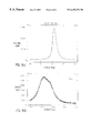
The milled sample was then subjected to bias temperature stressing (BTS) which was carried out at a temperature of 300° C. and a voltage of 2 Mv/cm for 5 hours. These conditions are normally sufficient to drive the Cu into the SiO2 dielectric layer. Thereafter, the sample was subjected to triangular voltage sweep (TVS) by varying the voltage and measuring the capacitance at a desired voltage. FIG. 5 shows the results of the TVS experiment. Specifically, FIG. 5 shows that two peaks are present in the sample. The peaks were determined to be sodium peaks that were originally present in the sample. No Al or Cu peaks were observed—this is evident in that no peaks are found in the negative voltage range wherein Cu typically resides—. The TVS data thus shows that the presence of the alpha-W barrier layer of the present invention prevents Cu from diffusing into the SiO2 dielectric layer.
The results of the above two experiments illustrate that the CVD deposited alpha-W is a robust diffusion barrier layer.
II. DEMONSTRATION OF ADHESION
Numerous samples of W on a SiO2 layer which was previously formed on a Si substrate were formed by the CVD method described above in a variety of thicknesses (3-100 nm) and structures consisting of both blanket films and long wire structures. Adhesion was tested using a scotch tape technique known to those skilled in the art and these test results revealed that the adhesion was invariably excellent (by the tape test) and remained so after temperature excursions as high as 750° C.
In a comparative study, W was deposited on a SiO2layer which was previously formed on a Si substrate by sputtering. Under the same high temperature excursion as the CVD deposited alpha-W, the wiring structures containing sputtered W delaminated.
III. DEMONSTRATION OF CONFORMAL COVERAGE
In current practice, it is only necessary to coat trenches which are typically about 0.3 microns wide with a 3:1 aspect ratio. To provide a rigorous test for conformal coverage, overhang structures were fabricated which had a base width of only about 0.05 microns and an aspect ratio of about 5:1. From the SEM data it can be seen that conformality of growth of alpha-W by CVD was so good that these structures could have been completely filled with alpha-W. This represents a much more difficult proposition than merely providing a coating to the walls. Thus, the conformal growth characteristics of the method far exceeds the conformal requirements of current practice.
IV. DEMONSTRATION OF THE STRUCTURAL DIFFERENCES BETWEEN ALPHA-W FORMED IN ACCORDANCE WITH THE PRESENT INVENTION AND SPUTTERED W
X-ray crystallography was used to characterized a first sample containing 50 nm sputtered W on a layer of SiO2 which was previously formed on a Si substrate and a second sample containing alpha-W which is formed on a layer of SiO2 which was previously formed on a Si substrate using the low temperature/pressure CVD process of the present invention. Reference is first made to FIG. 6(a) which shows the X-ray data for the CVD deposited W. Specifically, this figure shows a single symmetrical peak in the 2-theta diagram which is characteristic of 110 alpha-W. In regard to the sputtered W, reference is made to the X-ray data shown in FIG. 6(b). Specifically, FIG. 6(b) shows that the sputtered W contains both alpha-W and beta-W which is evident in that the peak is an asymmetric peak which contains two symmetric peaks inside thereof. This data clearly shows that sputtered W forms both the alpha-and beta-phases of W. As stated above, the presence of both phases is not desirable in obtaining a barrier layer which meets all seven of the criteria mentioned in the Background Section of the present application.
While this invention has been particularly shown and described with respect to preferred embodiments thereof, it will be understood by those skilled in the art that the foregoing and other changes in form and detail may be made without departing from the spirit and scope of the present invention.

Claims (22)

Having thus described our invention, what we claim as new, and desire to secure by Letters Patent is:
1. A barrier layer for use in an interconnect structure, said barrier layer comprising a single-phase alpha-W layer, wherein said alpha-W layer lines an opening formed in a dielectric material layer and has a thickness of less than 15 nm which substantially prevents out-diffusion of a Cu conductive material into said dielectric material layer.
2. The barrier layer of claim 1 wherein said alpha-W has a minimum thickness of no less than about 7 nm.
3. The barrier layer of claim 1 wherein said alpha-W is formed by chemical vapor deposition using W(CO)6 as the source material.
4. The barrier layer of claim 1 wherein said alpha-W barrier layer further includes hydrogen.
5. A structure comprising a first layer of dielectric material having at least one opening formed in a surface thereof, an alpha-W diffusion barrier layer lining said at least one opening, said alpha-W diffusion barrier layer is a single phase material having a thickness of less than 15 nm, and a conductor composed of Cu formed in said opening on said alpha-W diffusion barrier layer, wherein said Cu conductor is not in physical contact with said layer of dielectric material and said alpha-W layer substantially prevents outdiffusion of said Cu conductor into said first dielectric layer.
6. The structure of claim 5 further comprising a metal seed layer, said metal seed layer being formed between said alpha-W layer and said conductor.
7. The structure of claim 6 wherein said metal seed layer comprises substantially Cu.
8. The structure of claim 5 wherein said dielectric material is a polyimide, paralyne polymer, silicon polymer, diamond, diamond-like carbon, fluorinated diamond-like carbon, SiO2 or Si3N4.
9. The structure of claim 8 wherein said dielectric material is SiO2.
10. The structure of claim 5 wherein said alpha-W layer is formed by chemical vapor deposition using W(CO)6 as the source material.
11. The structure of claim 5 wherein said alpha-W layer has a minimum thickness of no less than 7.0 nm.
12. The structure of claim 5 wherein said dielectric material is doped with a dopant.
13. The structure of claim 12 wherein said dopant is fluorine, boron, silicon, Ge or phosphorous.
14. The structure of claim 5 wherein said alpha-W layer further includes hydrogen.
15. The structure of claim 5 wherein said layer of dielectric material is formed on a semiconductor substrate.
16. The structure of claim 15 wherein said semiconductor substrate is composed of Si, Ge, SiGe, InAs or InP.
17. The structure of claim 15 wherein another layer of alpha-W having a single phase is formed on top of said Cu conductor.
18. The structure of claim 15 wherein a barrier layer is formed on said first layer of dielectric material abutting said at least one opening and said Cu conductor is not restricted to said at least one opening.
19. The structure of claim 17 wherein an electrode is formed on said another layer of alpha-W.
20. The structure of claim 15 wherein a second layer of dielectric material is formed on said first layer of dielectric material, said second layer of dielectric material having at least one opening formed in a surface thereof, said openings in said second dielectric being formed on said openings of said first layer of dielectric material, an alpha-W diffusion barrier layer lining said at least one opening of said second layer of dielectric material, said alpha-W diffusion barrier layer is a single phase material having a thickness of less than 15 nm, and a conductor composed of Cu formed in said opening of said second layer of said dielectric material on said alpha-W diffusion barrier layer, wherein said conductor of said second layer of dielectric material is not in physical contact with any dielectric material layers.
21. The structure of claim 15 wherein said first layer of dielectric material is part of an interconnect structure.
22. The structure of claim 21 wherein said interconnect structure is a capacitor, a damascene structure or a wiring structure containing multi-vias and wiring levels.
US09/070,394 1998-04-30 1998-04-30 Ultra thin, single phase, diffusion barrier for metal conductors Expired - Fee Related US6452276B1 (en)

Priority Applications (8)

Application Number Priority Date Filing Date Title
US09/070,394 US6452276B1 (en) 1998-04-30 1998-04-30 Ultra thin, single phase, diffusion barrier for metal conductors
TW088101964A TW482826B (en) 1998-04-30 1999-02-09 Ultra thin, single phase, diffusion barrier for metal conductors
KR10-1999-0008451A KR100386529B1 (en) 1998-04-30 1999-03-13 Ultra thin, single phase, diffusion barrier for metal conductors
CNB991044428A CN1134060C (en) 1998-04-30 1999-03-29 Ultra thin, single phase, diffusion barrier for metal conductors
SG9901658A SG81271A1 (en) 1998-04-30 1999-04-12 Ultra thin, single phase, diffusion barrier for metal conductors
JP11757899A JP3177228B2 (en) 1998-04-30 1999-04-26 Ultra-thin single-phase barrier layers for conductors and their preparation
EP99303340A EP0954016A3 (en) 1998-04-30 1999-04-28 Diffusion barrier for metal conductors
US10/188,686 US7172968B2 (en) 1998-04-30 2002-07-03 Ultra thin, single phase, diffusion barrier for metal conductors

Applications Claiming Priority (1)

Application Number Priority Date Filing Date Title
US09/070,394 US6452276B1 (en) 1998-04-30 1998-04-30 Ultra thin, single phase, diffusion barrier for metal conductors

Related Child Applications (1)

Application Number Title Priority Date Filing Date
US10/188,686 Division US7172968B2 (en) 1998-04-30 2002-07-03 Ultra thin, single phase, diffusion barrier for metal conductors

Publications (1)

Publication Number Publication Date
US6452276B1 true US6452276B1 (en) 2002-09-17

Family

ID=22095033

Family Applications (2)

Application Number Title Priority Date Filing Date
US09/070,394 Expired - Fee Related US6452276B1 (en) 1998-04-30 1998-04-30 Ultra thin, single phase, diffusion barrier for metal conductors
US10/188,686 Expired - Fee Related US7172968B2 (en) 1998-04-30 2002-07-03 Ultra thin, single phase, diffusion barrier for metal conductors

Family Applications After (1)

Application Number Title Priority Date Filing Date
US10/188,686 Expired - Fee Related US7172968B2 (en) 1998-04-30 2002-07-03 Ultra thin, single phase, diffusion barrier for metal conductors

Country Status (7)

Country Link
US (2) US6452276B1 (en)
EP (1) EP0954016A3 (en)
JP (1) JP3177228B2 (en)
KR (1) KR100386529B1 (en)
CN (1) CN1134060C (en)
SG (1) SG81271A1 (en)
TW (1) TW482826B (en)

Cited By (17)

* Cited by examiner, † Cited by third party
Publication number Priority date Publication date Assignee Title
US20020038903A1 (en) * 2000-10-03 2002-04-04 Liming Tsau High density metal capacitor using dual-damascene copper interconnect
US6679997B2 (en) * 1998-08-12 2004-01-20 Nec Compound Semiconductor Devices, Ltd. Organic insulation film formation method
US6734560B2 (en) * 2001-10-02 2004-05-11 Lsi Logic Corporation Diamond barrier layer
US20040244590A1 (en) * 2003-05-02 2004-12-09 Worcester Polytechnic Institute Composite gas separation modules having high Tamman temperature intermediate layers
US20050113316A1 (en) * 2001-07-24 2005-05-26 Panagin Pharmaceuticals Inc. Process for producing dammarane sapogenins and ginsenosides
US20060016332A1 (en) * 2004-07-21 2006-01-26 Ma Yi H Composite gas separation modules having a layer of particles with a uniform binder metal distribution
US20080042282A1 (en) * 2000-05-08 2008-02-21 Tatsuyuki Saito Semiconductor integrated circuit device and a method of manufacturing the same
US20090134517A1 (en) * 2007-11-28 2009-05-28 Takamasa Usui Semiconductor device and method of manufacturing the same
US20100052178A1 (en) * 2008-08-29 2010-03-04 Dirk Meinhold Semiconductor Device and Method for Making Same
US20100132546A1 (en) * 2007-04-05 2010-06-03 Yi Hua Ma Composite Structures with Porous Anodic Oxide Layers and Methods of Fabrication
US8652239B2 (en) 2010-05-03 2014-02-18 Worcester Polytechnic Institute High permeance sulfur tolerant Pd/Cu alloy membranes
US20150092371A1 (en) * 2013-09-27 2015-04-02 Infineon Technologies Ag Contact pad structure, an electronic component, and a method for manufacturing a contact pad structure
US20160005692A1 (en) * 2013-09-27 2016-01-07 Intel Corporation Interconnects with fully clad lines
US20160049373A1 (en) * 2014-03-21 2016-02-18 Taiwan Semiconductor Manufacturing Co., Ltd. Via pre-fill on back-end-of-the-line interconnect layer
US20160163587A1 (en) * 2014-12-08 2016-06-09 International Business Machines Corporation Self-aligned via interconnect structures
US20170309490A1 (en) * 2014-09-24 2017-10-26 Hitachi Kokusai Electric Inc. Method of manufacturing semiconductor device
US20190074216A1 (en) * 2017-09-07 2019-03-07 Tokyo Electron Limited Semiconductor Device

Families Citing this family (25)

* Cited by examiner, † Cited by third party
Publication number Priority date Publication date Assignee Title
US6503375B1 (en) 2000-02-11 2003-01-07 Applied Materials, Inc Electroplating apparatus using a perforated phosphorus doped consumable anode
KR100472731B1 (en) * 2000-06-30 2005-03-08 주식회사 하이닉스반도체 Method for forming semiconductor device capable of omitting seed layer etch process
US6373087B1 (en) * 2000-08-31 2002-04-16 Agere Systems Guardian Corp. Methods of fabricating a metal-oxide-metal capacitor and associated apparatuses
TW523792B (en) * 2000-09-07 2003-03-11 Toshiba Corp Semiconductor device and its manufacturing method
US9076843B2 (en) 2001-05-22 2015-07-07 Novellus Systems, Inc. Method for producing ultra-thin tungsten layers with improved step coverage
US20060063025A1 (en) * 2004-04-07 2006-03-23 Jing-Yi Huang Method and system for making thin metal films
JP2006097099A (en) * 2004-09-30 2006-04-13 Tri Chemical Laboratory Inc Film deposition material, film deposition method and element
US8053365B2 (en) * 2007-12-21 2011-11-08 Novellus Systems, Inc. Methods for forming all tungsten contacts and lines
US20100267230A1 (en) 2009-04-16 2010-10-21 Anand Chandrashekar Method for forming tungsten contacts and interconnects with small critical dimensions
US9159571B2 (en) 2009-04-16 2015-10-13 Lam Research Corporation Tungsten deposition process using germanium-containing reducing agent
US10256142B2 (en) 2009-08-04 2019-04-09 Novellus Systems, Inc. Tungsten feature fill with nucleation inhibition
CN113862634A (en) 2012-03-27 2021-12-31 诺发系统公司 Tungsten feature fill
US8853080B2 (en) 2012-09-09 2014-10-07 Novellus Systems, Inc. Method for depositing tungsten film with low roughness and low resistivity
US9153486B2 (en) 2013-04-12 2015-10-06 Lam Research Corporation CVD based metal/semiconductor OHMIC contact for high volume manufacturing applications
US9589808B2 (en) 2013-12-19 2017-03-07 Lam Research Corporation Method for depositing extremely low resistivity tungsten
CN104157607B (en) * 2014-09-01 2017-02-15 上海先进半导体制造股份有限公司 Optimization method for back side pressure in tungsten deposition process
US9583462B2 (en) * 2015-01-22 2017-02-28 Qualcomm Incorporated Damascene re-distribution layer (RDL) in fan out split die application
US9953984B2 (en) 2015-02-11 2018-04-24 Lam Research Corporation Tungsten for wordline applications
US9613818B2 (en) 2015-05-27 2017-04-04 Lam Research Corporation Deposition of low fluorine tungsten by sequential CVD process
US9754824B2 (en) 2015-05-27 2017-09-05 Lam Research Corporation Tungsten films having low fluorine content
US9978605B2 (en) 2015-05-27 2018-05-22 Lam Research Corporation Method of forming low resistivity fluorine free tungsten film without nucleation
US11348795B2 (en) 2017-08-14 2022-05-31 Lam Research Corporation Metal fill process for three-dimensional vertical NAND wordline
CN112262457A (en) 2018-05-03 2021-01-22 朗姆研究公司 Methods of depositing tungsten and other metals in 3D NAND structures
US11476267B2 (en) * 2019-05-24 2022-10-18 Applied Materials, Inc. Liner for V-NAND word line stack
US11670547B2 (en) 2021-01-15 2023-06-06 Taiwan Semiconductor Manufacturing Company, Ltd. Semiconductor arrangement and method of making

Citations (11)

* Cited by examiner, † Cited by third party
Publication number Priority date Publication date Assignee Title
US3639165A (en) * 1968-06-20 1972-02-01 Gen Electric Resistor thin films formed by low-pressure deposition of molybdenum and tungsten
US4902645A (en) * 1987-08-24 1990-02-20 Fujitsu Limited Method of selectively forming a silicon-containing metal layer
JPH02307210A (en) * 1989-05-22 1990-12-20 Matsushita Electron Corp Manufacture of x-ray mask
US5126825A (en) * 1989-07-26 1992-06-30 Oki Electric Industry Co., Ltd. Wiring structure of a semiconductor device with beta tungsten
US5232872A (en) * 1989-05-09 1993-08-03 Fujitsu Limited Method for manufacturing semiconductor device
JPH05259110A (en) 1992-03-12 1993-10-08 Sony Corp Formation method of metal plug in semiconductor device
US5429989A (en) * 1994-02-03 1995-07-04 Motorola, Inc. Process for fabricating a metallization structure in a semiconductor device
JPH08298285A (en) 1995-04-27 1996-11-12 Oki Electric Ind Co Ltd Semiconductor element and its manufacture
US5693563A (en) * 1996-07-15 1997-12-02 Chartered Semiconductor Manufacturing Pte Ltd. Etch stop for copper damascene process
JPH108251A (en) 1996-06-19 1998-01-13 Fujitsu Ltd Production of semiconductor device
US5789312A (en) * 1996-10-30 1998-08-04 International Business Machines Corporation Method of fabricating mid-gap metal gates compatible with ultra-thin dielectrics

Family Cites Families (21)

* Cited by examiner, † Cited by third party
Publication number Priority date Publication date Assignee Title
US4451503A (en) 1982-06-30 1984-05-29 International Business Machines Corporation Photo deposition of metals with far UV radiation
JPS59132136A (en) 1983-01-19 1984-07-30 Hitachi Ltd Manufacture of semiconductor device
US4817557A (en) 1983-05-23 1989-04-04 Anicon, Inc. Process and apparatus for low pressure chemical vapor deposition of refractory metal
US4619840A (en) 1983-05-23 1986-10-28 Thermco Systems, Inc. Process and apparatus for low pressure chemical vapor deposition of refractory metal
JPS61217576A (en) 1985-03-20 1986-09-27 Hitachi Ltd Formation of thin tungsten film
US4741928A (en) * 1985-12-27 1988-05-03 General Electric Company Method for selective deposition of tungsten by chemical vapor deposition onto metal and semiconductor surfaces
KR900003618B1 (en) * 1986-05-30 1990-05-26 후지쓰가부시끼가이샤 Semiconductor device
US4924295A (en) * 1986-11-28 1990-05-08 Siemens Aktiengesellschaft Integrated semi-conductor circuit comprising at least two metallization levels composed of aluminum or aluminum compounds and a method for the manufacture of same
US5212400A (en) 1988-02-18 1993-05-18 International Business Machines Corporation Method of depositing tungsten on silicon in a non-self-limiting CVD process and semiconductor device manufactured thereby
US4926237A (en) * 1988-04-04 1990-05-15 Motorola, Inc. Device metallization, device and method
US5316974A (en) * 1988-12-19 1994-05-31 Texas Instruments Incorporated Integrated circuit copper metallization process using a lift-off seed layer and a thick-plated conductor layer
JPH0475750U (en) * 1990-11-15 1992-07-02
EP0575688B1 (en) 1992-06-26 1998-05-27 STMicroelectronics S.r.l. Programming of LDD-ROM cells
US5583067A (en) * 1993-01-22 1996-12-10 Intel Corporation Inverse T-gate semiconductor device with self-aligned punchthrough stops and method of fabrication
US5539230A (en) 1995-03-16 1996-07-23 International Business Machines Corporation Chimney capacitor
JP3422345B2 (en) * 1995-05-31 2003-06-30 日本電信電話株式会社 Method of forming tungsten film
JP3353874B2 (en) * 1996-09-24 2002-12-03 シャープ株式会社 Semiconductor device and manufacturing method thereof
US5847462A (en) * 1996-11-14 1998-12-08 Advanced Micro Devices, Inc. Integrated circuit having conductors of enhanced cross-sectional area with etch stop barrier layer
US6713391B2 (en) * 1997-07-11 2004-03-30 Honeywell International Inc. Physical vapor deposition targets
US6271128B1 (en) * 2000-09-29 2001-08-07 Vanguard International Semiconductor Corp. Method for fabricating transistor
JP2003068848A (en) * 2001-08-29 2003-03-07 Fujitsu Ltd Semiconductor device and its manufacturing method

Patent Citations (11)

* Cited by examiner, † Cited by third party
Publication number Priority date Publication date Assignee Title
US3639165A (en) * 1968-06-20 1972-02-01 Gen Electric Resistor thin films formed by low-pressure deposition of molybdenum and tungsten
US4902645A (en) * 1987-08-24 1990-02-20 Fujitsu Limited Method of selectively forming a silicon-containing metal layer
US5232872A (en) * 1989-05-09 1993-08-03 Fujitsu Limited Method for manufacturing semiconductor device
JPH02307210A (en) * 1989-05-22 1990-12-20 Matsushita Electron Corp Manufacture of x-ray mask
US5126825A (en) * 1989-07-26 1992-06-30 Oki Electric Industry Co., Ltd. Wiring structure of a semiconductor device with beta tungsten
JPH05259110A (en) 1992-03-12 1993-10-08 Sony Corp Formation method of metal plug in semiconductor device
US5429989A (en) * 1994-02-03 1995-07-04 Motorola, Inc. Process for fabricating a metallization structure in a semiconductor device
JPH08298285A (en) 1995-04-27 1996-11-12 Oki Electric Ind Co Ltd Semiconductor element and its manufacture
JPH108251A (en) 1996-06-19 1998-01-13 Fujitsu Ltd Production of semiconductor device
US5693563A (en) * 1996-07-15 1997-12-02 Chartered Semiconductor Manufacturing Pte Ltd. Etch stop for copper damascene process
US5789312A (en) * 1996-10-30 1998-08-04 International Business Machines Corporation Method of fabricating mid-gap metal gates compatible with ultra-thin dielectrics

Non-Patent Citations (1)

* Cited by examiner, † Cited by third party
Title
Maeda, K., "VLSI and CVDs" Jul. 31, 1997, pp. 80-82.

Cited By (38)

* Cited by examiner, † Cited by third party
Publication number Priority date Publication date Assignee Title
US6679997B2 (en) * 1998-08-12 2004-01-20 Nec Compound Semiconductor Devices, Ltd. Organic insulation film formation method
US20080042282A1 (en) * 2000-05-08 2008-02-21 Tatsuyuki Saito Semiconductor integrated circuit device and a method of manufacturing the same
US7642652B2 (en) * 2000-05-08 2010-01-05 Renesas Technology Corp. Semiconductor integrated circuit device and a method of manufacturing the same
US20050161765A1 (en) * 2000-10-03 2005-07-28 Broadcom Corporation High-density metal capacitor using dual-damascene copper interconnect
US7187015B2 (en) 2000-10-03 2007-03-06 Broadcom Corporation High-density metal capacitor using dual-damascene copper interconnect
US6833604B2 (en) * 2000-10-03 2004-12-21 Broadcom Corporation High density metal capacitor using dual-damascene copper interconnect
US20020038903A1 (en) * 2000-10-03 2002-04-04 Liming Tsau High density metal capacitor using dual-damascene copper interconnect
US6902972B2 (en) 2000-10-03 2005-06-07 Broadcom Corporation High-density metal capacitor using dual-damascene copper interconnect
US20040232520A1 (en) * 2000-10-03 2004-11-25 Liming Tsau High-density metal capacitor using dual-damascene copper interconnect
US20050113316A1 (en) * 2001-07-24 2005-05-26 Panagin Pharmaceuticals Inc. Process for producing dammarane sapogenins and ginsenosides
US6734560B2 (en) * 2001-10-02 2004-05-11 Lsi Logic Corporation Diamond barrier layer
US20040244590A1 (en) * 2003-05-02 2004-12-09 Worcester Polytechnic Institute Composite gas separation modules having high Tamman temperature intermediate layers
US7255726B2 (en) 2003-05-02 2007-08-14 Worcester Polytechnic Institute Composite gas separation modules having high Tamman temperature intermediate layers
US20060016332A1 (en) * 2004-07-21 2006-01-26 Ma Yi H Composite gas separation modules having a layer of particles with a uniform binder metal distribution
US7727596B2 (en) 2004-07-21 2010-06-01 Worcester Polytechnic Institute Method for fabricating a composite gas separation module
US20100132546A1 (en) * 2007-04-05 2010-06-03 Yi Hua Ma Composite Structures with Porous Anodic Oxide Layers and Methods of Fabrication
US8366805B2 (en) 2007-04-05 2013-02-05 Worcester Polytechnic Institute Composite structures with porous anodic oxide layers and methods of fabrication
US7944053B2 (en) * 2007-11-28 2011-05-17 Kabushiki Kaisha Toshiba Semiconductor device and method of manufacturing the same
US20090134517A1 (en) * 2007-11-28 2009-05-28 Takamasa Usui Semiconductor device and method of manufacturing the same
US9263328B2 (en) 2008-08-29 2016-02-16 Infineon Technologies Ag Semiconductor device and method for making same
US8994179B2 (en) * 2008-08-29 2015-03-31 Infineon Technologies Ag Semiconductor device and method for making same
US20100052178A1 (en) * 2008-08-29 2010-03-04 Dirk Meinhold Semiconductor Device and Method for Making Same
US9312172B2 (en) 2008-08-29 2016-04-12 Infineon Technologies Ag Semiconductor device and method for making same
US8652239B2 (en) 2010-05-03 2014-02-18 Worcester Polytechnic Institute High permeance sulfur tolerant Pd/Cu alloy membranes
US9385085B2 (en) * 2013-09-27 2016-07-05 Intel Corporation Interconnects with fully clad lines
US20160005692A1 (en) * 2013-09-27 2016-01-07 Intel Corporation Interconnects with fully clad lines
US20150092371A1 (en) * 2013-09-27 2015-04-02 Infineon Technologies Ag Contact pad structure, an electronic component, and a method for manufacturing a contact pad structure
US9723716B2 (en) * 2013-09-27 2017-08-01 Infineon Technologies Ag Contact pad structure, an electronic component, and a method for manufacturing a contact pad structure
US9728503B2 (en) * 2014-03-21 2017-08-08 Taiwan Semiconductor Manufacturing Co., Ltd. Via pre-fill on back-end-of-the-line interconnect layer
US20160049373A1 (en) * 2014-03-21 2016-02-18 Taiwan Semiconductor Manufacturing Co., Ltd. Via pre-fill on back-end-of-the-line interconnect layer
US20170309490A1 (en) * 2014-09-24 2017-10-26 Hitachi Kokusai Electric Inc. Method of manufacturing semiconductor device
US20160163587A1 (en) * 2014-12-08 2016-06-09 International Business Machines Corporation Self-aligned via interconnect structures
US10727122B2 (en) * 2014-12-08 2020-07-28 International Business Machines Corporation Self-aligned via interconnect structures
US11348832B2 (en) 2014-12-08 2022-05-31 International Business Machines Corporation Self-aligned via interconnect structures
US20190074216A1 (en) * 2017-09-07 2019-03-07 Tokyo Electron Limited Semiconductor Device
KR20190027733A (en) * 2017-09-07 2019-03-15 도쿄엘렉트론가부시키가이샤 Semiconductor device
KR102177575B1 (en) 2017-09-07 2020-11-11 도쿄엘렉트론가부시키가이샤 Semiconductor device
US11211288B2 (en) * 2017-09-07 2021-12-28 Tokyo Electron Limited Semiconductor device

Also Published As

Publication number Publication date
JP3177228B2 (en) 2001-06-18
CN1134060C (en) 2004-01-07
EP0954016A3 (en) 2002-07-17
US20020175418A1 (en) 2002-11-28
KR19990082732A (en) 1999-11-25
SG81271A1 (en) 2001-06-19
US7172968B2 (en) 2007-02-06
KR100386529B1 (en) 2003-06-02
CN1233852A (en) 1999-11-03
TW482826B (en) 2002-04-11
JPH11330006A (en) 1999-11-30
EP0954016A2 (en) 1999-11-03

Similar Documents

Publication Publication Date Title
US6452276B1 (en) Ultra thin, single phase, diffusion barrier for metal conductors
EP1114449B1 (en) Method for forming a capacitor with a ruthenium silicide diffusion barrier layer
JP4180145B2 (en) Semiconductor device formation method
KR100441190B1 (en) Diffusion barrier layers and methods of forming same
US7154178B2 (en) Multilayer diffusion barrier for copper interconnections
JP4314413B2 (en) Ta ▲ Lower2 ▼ O ▲ Lower5 Dielectric layer manufacturing method
US7153773B2 (en) TiSiN film forming method, diffusion barrier TiSiN film, semiconductor device, method of fabricating the same and TiSiN film forming system
US6399490B1 (en) Highly conformal titanium nitride deposition process for high aspect ratio structures
US5677244A (en) Method of alloying an interconnect structure with copper
US7144803B2 (en) Methods of forming boron carbo-nitride layers for integrated circuit devices
JP4168397B2 (en) Boron doped titanium nitride layer for high aspect ratio semiconductor devices
US6613669B2 (en) Semiconductor device and method for manufacturing the same
US20030042606A1 (en) Method of forming a conductive contact
EP0587401A2 (en) Manufacture of a plug or a via in a semiconductor device
KR100289515B1 (en) Barrier emtal layer and method of forming the same
US5994218A (en) Method of forming electrical connections for a semiconductor device

Legal Events

Date Code Title Description
AS Assignment

Owner name: INTERNATIONAL BUSINESS MACHINES CORPORATION, NEW Y

Free format text: ASSIGNMENT OF ASSIGNORS INTEREST;ASSIGNORS:COHEN, STEPHEN A.;MCFEELY, FENTON R.;NOYAN, CEVDET I.;AND OTHERS;REEL/FRAME:009358/0805;SIGNING DATES FROM 19980702 TO 19980729

AS Assignment

Owner name: INTERNATIONAL BUSINESS MACHINES CORPORATION, NEW Y

Free format text: ASSIGNMENT OF ASSIGNORS INTEREST;ASSIGNORS:COHEN, STEPHAN A.;MCFEELY, FENTON R.;NOYAN, CEVDET I.;AND OTHERS;REEL/FRAME:009616/0378;SIGNING DATES FROM 19981026 TO 19981105

FEPP Fee payment procedure

Free format text: PAYOR NUMBER ASSIGNED (ORIGINAL EVENT CODE: ASPN); ENTITY STATUS OF PATENT OWNER: LARGE ENTITY

CC Certificate of correction
FPAY Fee payment

Year of fee payment: 4

REMI Maintenance fee reminder mailed
LAPS Lapse for failure to pay maintenance fees
STCH Information on status: patent discontinuation

Free format text: PATENT EXPIRED DUE TO NONPAYMENT OF MAINTENANCE FEES UNDER 37 CFR 1.362

FP Lapsed due to failure to pay maintenance fee

Effective date: 20100917

AS Assignment

Owner name: GLOBALFOUNDRIES U.S. 2 LLC, NEW YORK

Free format text: ASSIGNMENT OF ASSIGNORS INTEREST;ASSIGNOR:INTERNATIONAL BUSINESS MACHINES CORPORATION;REEL/FRAME:036550/0001

Effective date: 20150629

AS Assignment

Owner name: GLOBALFOUNDRIES INC., CAYMAN ISLANDS

Free format text: ASSIGNMENT OF ASSIGNORS INTEREST;ASSIGNORS:GLOBALFOUNDRIES U.S. 2 LLC;GLOBALFOUNDRIES U.S. INC.;REEL/FRAME:036779/0001

Effective date: 20150910