US6472758B1 - Semiconductor package including stacked semiconductor dies and bond wires - Google Patents
Semiconductor package including stacked semiconductor dies and bond wires Download PDFInfo
- Publication number
- US6472758B1 US6472758B1 US09/620,444 US62044400A US6472758B1 US 6472758 B1 US6472758 B1 US 6472758B1 US 62044400 A US62044400 A US 62044400A US 6472758 B1 US6472758 B1 US 6472758B1
- Authority
- US
- United States
- Prior art keywords
- die
- adhesive
- dies
- semiconductor
- layer
- Prior art date
- Legal status (The legal status is an assumption and is not a legal conclusion. Google has not performed a legal analysis and makes no representation as to the accuracy of the status listed.)
- Expired - Lifetime
Links
Images


Classifications
-
- H—ELECTRICITY
- H01—ELECTRIC ELEMENTS
- H01L—SEMICONDUCTOR DEVICES NOT COVERED BY CLASS H10
- H01L25/00—Assemblies consisting of a plurality of individual semiconductor or other solid state devices ; Multistep manufacturing processes thereof
- H01L25/03—Assemblies consisting of a plurality of individual semiconductor or other solid state devices ; Multistep manufacturing processes thereof all the devices being of a type provided for in the same subgroup of groups H01L27/00 - H01L33/00, or in a single subclass of H10K, H10N, e.g. assemblies of rectifier diodes
- H01L25/04—Assemblies consisting of a plurality of individual semiconductor or other solid state devices ; Multistep manufacturing processes thereof all the devices being of a type provided for in the same subgroup of groups H01L27/00 - H01L33/00, or in a single subclass of H10K, H10N, e.g. assemblies of rectifier diodes the devices not having separate containers
- H01L25/065—Assemblies consisting of a plurality of individual semiconductor or other solid state devices ; Multistep manufacturing processes thereof all the devices being of a type provided for in the same subgroup of groups H01L27/00 - H01L33/00, or in a single subclass of H10K, H10N, e.g. assemblies of rectifier diodes the devices not having separate containers the devices being of a type provided for in group H01L27/00
- H01L25/0657—Stacked arrangements of devices
-
- H—ELECTRICITY
- H01—ELECTRIC ELEMENTS
- H01L—SEMICONDUCTOR DEVICES NOT COVERED BY CLASS H10
- H01L2224/00—Indexing scheme for arrangements for connecting or disconnecting semiconductor or solid-state bodies and methods related thereto as covered by H01L24/00
- H01L2224/01—Means for bonding being attached to, or being formed on, the surface to be connected, e.g. chip-to-package, die-attach, "first-level" interconnects; Manufacturing methods related thereto
- H01L2224/02—Bonding areas; Manufacturing methods related thereto
- H01L2224/04—Structure, shape, material or disposition of the bonding areas prior to the connecting process
- H01L2224/05—Structure, shape, material or disposition of the bonding areas prior to the connecting process of an individual bonding area
- H01L2224/0554—External layer
- H01L2224/0555—Shape
- H01L2224/05552—Shape in top view
- H01L2224/05553—Shape in top view being rectangular
-
- H—ELECTRICITY
- H01—ELECTRIC ELEMENTS
- H01L—SEMICONDUCTOR DEVICES NOT COVERED BY CLASS H10
- H01L2224/00—Indexing scheme for arrangements for connecting or disconnecting semiconductor or solid-state bodies and methods related thereto as covered by H01L24/00
- H01L2224/01—Means for bonding being attached to, or being formed on, the surface to be connected, e.g. chip-to-package, die-attach, "first-level" interconnects; Manufacturing methods related thereto
- H01L2224/26—Layer connectors, e.g. plate connectors, solder or adhesive layers; Manufacturing methods related thereto
- H01L2224/31—Structure, shape, material or disposition of the layer connectors after the connecting process
- H01L2224/32—Structure, shape, material or disposition of the layer connectors after the connecting process of an individual layer connector
- H01L2224/321—Disposition
- H01L2224/32135—Disposition the layer connector connecting between different semiconductor or solid-state bodies, i.e. chip-to-chip
- H01L2224/32145—Disposition the layer connector connecting between different semiconductor or solid-state bodies, i.e. chip-to-chip the bodies being stacked
-
- H—ELECTRICITY
- H01—ELECTRIC ELEMENTS
- H01L—SEMICONDUCTOR DEVICES NOT COVERED BY CLASS H10
- H01L2224/00—Indexing scheme for arrangements for connecting or disconnecting semiconductor or solid-state bodies and methods related thereto as covered by H01L24/00
- H01L2224/01—Means for bonding being attached to, or being formed on, the surface to be connected, e.g. chip-to-package, die-attach, "first-level" interconnects; Manufacturing methods related thereto
- H01L2224/26—Layer connectors, e.g. plate connectors, solder or adhesive layers; Manufacturing methods related thereto
- H01L2224/31—Structure, shape, material or disposition of the layer connectors after the connecting process
- H01L2224/32—Structure, shape, material or disposition of the layer connectors after the connecting process of an individual layer connector
- H01L2224/321—Disposition
- H01L2224/32151—Disposition the layer connector connecting between a semiconductor or solid-state body and an item not being a semiconductor or solid-state body, e.g. chip-to-substrate, chip-to-passive
- H01L2224/32221—Disposition the layer connector connecting between a semiconductor or solid-state body and an item not being a semiconductor or solid-state body, e.g. chip-to-substrate, chip-to-passive the body and the item being stacked
- H01L2224/32225—Disposition the layer connector connecting between a semiconductor or solid-state body and an item not being a semiconductor or solid-state body, e.g. chip-to-substrate, chip-to-passive the body and the item being stacked the item being non-metallic, e.g. insulating substrate with or without metallisation
-
- H—ELECTRICITY
- H01—ELECTRIC ELEMENTS
- H01L—SEMICONDUCTOR DEVICES NOT COVERED BY CLASS H10
- H01L2224/00—Indexing scheme for arrangements for connecting or disconnecting semiconductor or solid-state bodies and methods related thereto as covered by H01L24/00
- H01L2224/01—Means for bonding being attached to, or being formed on, the surface to be connected, e.g. chip-to-package, die-attach, "first-level" interconnects; Manufacturing methods related thereto
- H01L2224/42—Wire connectors; Manufacturing methods related thereto
- H01L2224/47—Structure, shape, material or disposition of the wire connectors after the connecting process
- H01L2224/48—Structure, shape, material or disposition of the wire connectors after the connecting process of an individual wire connector
- H01L2224/481—Disposition
- H01L2224/48151—Connecting between a semiconductor or solid-state body and an item not being a semiconductor or solid-state body, e.g. chip-to-substrate, chip-to-passive
- H01L2224/48221—Connecting between a semiconductor or solid-state body and an item not being a semiconductor or solid-state body, e.g. chip-to-substrate, chip-to-passive the body and the item being stacked
- H01L2224/48225—Connecting between a semiconductor or solid-state body and an item not being a semiconductor or solid-state body, e.g. chip-to-substrate, chip-to-passive the body and the item being stacked the item being non-metallic, e.g. insulating substrate with or without metallisation
- H01L2224/48227—Connecting between a semiconductor or solid-state body and an item not being a semiconductor or solid-state body, e.g. chip-to-substrate, chip-to-passive the body and the item being stacked the item being non-metallic, e.g. insulating substrate with or without metallisation connecting the wire to a bond pad of the item
-
- H—ELECTRICITY
- H01—ELECTRIC ELEMENTS
- H01L—SEMICONDUCTOR DEVICES NOT COVERED BY CLASS H10
- H01L2224/00—Indexing scheme for arrangements for connecting or disconnecting semiconductor or solid-state bodies and methods related thereto as covered by H01L24/00
- H01L2224/01—Means for bonding being attached to, or being formed on, the surface to be connected, e.g. chip-to-package, die-attach, "first-level" interconnects; Manufacturing methods related thereto
- H01L2224/42—Wire connectors; Manufacturing methods related thereto
- H01L2224/47—Structure, shape, material or disposition of the wire connectors after the connecting process
- H01L2224/48—Structure, shape, material or disposition of the wire connectors after the connecting process of an individual wire connector
- H01L2224/484—Connecting portions
- H01L2224/4847—Connecting portions the connecting portion on the bonding area of the semiconductor or solid-state body being a wedge bond
- H01L2224/48472—Connecting portions the connecting portion on the bonding area of the semiconductor or solid-state body being a wedge bond the other connecting portion not on the bonding area also being a wedge bond, i.e. wedge-to-wedge
-
- H—ELECTRICITY
- H01—ELECTRIC ELEMENTS
- H01L—SEMICONDUCTOR DEVICES NOT COVERED BY CLASS H10
- H01L2224/00—Indexing scheme for arrangements for connecting or disconnecting semiconductor or solid-state bodies and methods related thereto as covered by H01L24/00
- H01L2224/01—Means for bonding being attached to, or being formed on, the surface to be connected, e.g. chip-to-package, die-attach, "first-level" interconnects; Manufacturing methods related thereto
- H01L2224/42—Wire connectors; Manufacturing methods related thereto
- H01L2224/47—Structure, shape, material or disposition of the wire connectors after the connecting process
- H01L2224/49—Structure, shape, material or disposition of the wire connectors after the connecting process of a plurality of wire connectors
- H01L2224/491—Disposition
- H01L2224/4912—Layout
- H01L2224/49171—Fan-out arrangements
-
- H—ELECTRICITY
- H01—ELECTRIC ELEMENTS
- H01L—SEMICONDUCTOR DEVICES NOT COVERED BY CLASS H10
- H01L2224/00—Indexing scheme for arrangements for connecting or disconnecting semiconductor or solid-state bodies and methods related thereto as covered by H01L24/00
- H01L2224/73—Means for bonding being of different types provided for in two or more of groups H01L2224/10, H01L2224/18, H01L2224/26, H01L2224/34, H01L2224/42, H01L2224/50, H01L2224/63, H01L2224/71
- H01L2224/732—Location after the connecting process
- H01L2224/73251—Location after the connecting process on different surfaces
- H01L2224/73265—Layer and wire connectors
-
- H—ELECTRICITY
- H01—ELECTRIC ELEMENTS
- H01L—SEMICONDUCTOR DEVICES NOT COVERED BY CLASS H10
- H01L2224/00—Indexing scheme for arrangements for connecting or disconnecting semiconductor or solid-state bodies and methods related thereto as covered by H01L24/00
- H01L2224/80—Methods for connecting semiconductor or other solid state bodies using means for bonding being attached to, or being formed on, the surface to be connected
- H01L2224/83—Methods for connecting semiconductor or other solid state bodies using means for bonding being attached to, or being formed on, the surface to be connected using a layer connector
- H01L2224/8312—Aligning
- H01L2224/83136—Aligning involving guiding structures, e.g. spacers or supporting members
- H01L2224/83138—Aligning involving guiding structures, e.g. spacers or supporting members the guiding structures being at least partially left in the finished device
- H01L2224/83139—Guiding structures on the body
-
- H—ELECTRICITY
- H01—ELECTRIC ELEMENTS
- H01L—SEMICONDUCTOR DEVICES NOT COVERED BY CLASS H10
- H01L2225/00—Details relating to assemblies covered by the group H01L25/00 but not provided for in its subgroups
- H01L2225/03—All the devices being of a type provided for in the same subgroup of groups H01L27/00 - H01L33/648 and H10K99/00
- H01L2225/04—All the devices being of a type provided for in the same subgroup of groups H01L27/00 - H01L33/648 and H10K99/00 the devices not having separate containers
- H01L2225/065—All the devices being of a type provided for in the same subgroup of groups H01L27/00 - H01L33/648 and H10K99/00 the devices not having separate containers the devices being of a type provided for in group H01L27/00
- H01L2225/06503—Stacked arrangements of devices
- H01L2225/0651—Wire or wire-like electrical connections from device to substrate
-
- H—ELECTRICITY
- H01—ELECTRIC ELEMENTS
- H01L—SEMICONDUCTOR DEVICES NOT COVERED BY CLASS H10
- H01L2225/00—Details relating to assemblies covered by the group H01L25/00 but not provided for in its subgroups
- H01L2225/03—All the devices being of a type provided for in the same subgroup of groups H01L27/00 - H01L33/648 and H10K99/00
- H01L2225/04—All the devices being of a type provided for in the same subgroup of groups H01L27/00 - H01L33/648 and H10K99/00 the devices not having separate containers
- H01L2225/065—All the devices being of a type provided for in the same subgroup of groups H01L27/00 - H01L33/648 and H10K99/00 the devices not having separate containers the devices being of a type provided for in group H01L27/00
- H01L2225/06503—Stacked arrangements of devices
- H01L2225/06575—Auxiliary carrier between devices, the carrier having no electrical connection structure
-
- H—ELECTRICITY
- H01—ELECTRIC ELEMENTS
- H01L—SEMICONDUCTOR DEVICES NOT COVERED BY CLASS H10
- H01L2225/00—Details relating to assemblies covered by the group H01L25/00 but not provided for in its subgroups
- H01L2225/03—All the devices being of a type provided for in the same subgroup of groups H01L27/00 - H01L33/648 and H10K99/00
- H01L2225/04—All the devices being of a type provided for in the same subgroup of groups H01L27/00 - H01L33/648 and H10K99/00 the devices not having separate containers
- H01L2225/065—All the devices being of a type provided for in the same subgroup of groups H01L27/00 - H01L33/648 and H10K99/00 the devices not having separate containers the devices being of a type provided for in group H01L27/00
- H01L2225/06503—Stacked arrangements of devices
- H01L2225/06582—Housing for the assembly, e.g. chip scale package [CSP]
- H01L2225/06586—Housing with external bump or bump-like connectors
-
- H—ELECTRICITY
- H01—ELECTRIC ELEMENTS
- H01L—SEMICONDUCTOR DEVICES NOT COVERED BY CLASS H10
- H01L2924/00—Indexing scheme for arrangements or methods for connecting or disconnecting semiconductor or solid-state bodies as covered by H01L24/00
- H01L2924/01—Chemical elements
- H01L2924/01079—Gold [Au]
-
- H—ELECTRICITY
- H01—ELECTRIC ELEMENTS
- H01L—SEMICONDUCTOR DEVICES NOT COVERED BY CLASS H10
- H01L2924/00—Indexing scheme for arrangements or methods for connecting or disconnecting semiconductor or solid-state bodies as covered by H01L24/00
- H01L2924/15—Details of package parts other than the semiconductor or other solid state devices to be connected
- H01L2924/151—Die mounting substrate
- H01L2924/153—Connection portion
- H01L2924/1531—Connection portion the connection portion being formed only on the surface of the substrate opposite to the die mounting surface
- H01L2924/15311—Connection portion the connection portion being formed only on the surface of the substrate opposite to the die mounting surface being a ball array, e.g. BGA
-
- H—ELECTRICITY
- H01—ELECTRIC ELEMENTS
- H01L—SEMICONDUCTOR DEVICES NOT COVERED BY CLASS H10
- H01L2924/00—Indexing scheme for arrangements or methods for connecting or disconnecting semiconductor or solid-state bodies as covered by H01L24/00
- H01L2924/15—Details of package parts other than the semiconductor or other solid state devices to be connected
- H01L2924/181—Encapsulation
-
- Y—GENERAL TAGGING OF NEW TECHNOLOGICAL DEVELOPMENTS; GENERAL TAGGING OF CROSS-SECTIONAL TECHNOLOGIES SPANNING OVER SEVERAL SECTIONS OF THE IPC; TECHNICAL SUBJECTS COVERED BY FORMER USPC CROSS-REFERENCE ART COLLECTIONS [XRACs] AND DIGESTS
- Y10—TECHNICAL SUBJECTS COVERED BY FORMER USPC
- Y10T—TECHNICAL SUBJECTS COVERED BY FORMER US CLASSIFICATION
- Y10T428/00—Stock material or miscellaneous articles
- Y10T428/21—Circular sheet or circular blank
Definitions
- This invention pertains to semiconductor packaging in general, and in particular, to a method and apparatus for making semiconductor packages with stacked dies.
- die-stacking techniques may be found, for example, in U.S. Pat. No. 5,323,060 to R. Fogel, et al.; U.S. Pat. No. 5,815,372 to W. N. Gallas; Re. Pat. No. 36,613 to M. B. Ball; U.S. Pat. No. 5,721,452 to R. Fogel, et al.; and, Japanese Patent Disclosures 62-126661, 4-56262, 63-128736, and 10-256470.
- FIGS. 1 and 2 are respectively a top plan and a cross-sectional side elevation view of a semiconductor package 10 incorporating a pair of stacked dies 14 and 16 in accordance with the respective methods and apparatus of the prior art.
- the package 10 illustrated is a ball grid array (“BGA”) type of package, so-called because of the balls of solder 19 formed on the bottom surfaces of the substrate 12 , which function as input/output terminals of the package.
- the package 10 includes a conventional interconnective substrate 12 and a first semiconductor die 14 mounted on a top surface of the substrate.
- a second die 16 has been “stacked,” i.e., mounted, on top of the first die 14 .
- the dies 14 and 16 typically include a plurality of input/output wire bonding pads 34 located at the peripheral edges of their respective top, or “active,” surfaces.
- the substrate 12 may comprise a flexible resin tape, a rigid fiber-glass/copper sheet laminate, a co-fired ceramic coupon, or a metal lead frame, all of known types in the industry, depending on the particular type of semiconductor package 10 at hand.
- the connective substrate 12 illustrated in the BGA package 10 shown in FIGS. 1 and 2 comprises a layer 20 (see FIG. 2) of an insulative material, e.g., a polyimide resin film, laminated between conductive layers 22 , 24 of a metal, e.g., copper or aluminum, that comprise the respective top and bottom surfaces of the substrate.
- an insulative material e.g., a polyimide resin film
- the conductive layers 22 , 24 are typically patterned, e.g., by photolithography and etching techniques, to define wire bonding pads 26 and circuit traces 27 in the top layer 22 , and solder ball mounting lands 28 in the bottom layer 24 .
- the terminal pads 26 and traces 27 are typically connected to the solder ball lands 28 through the thickness of the insulative layer 20 by “vias” 30 , i.e., plated-through holes in the layers.
- Either or both of the conductive layers 22 , 24 may be coated over with an insulative “solder mask” (not illustrated) that has openings in it through which the respective wire bonding pads 26 and/or solder ball lands 28 are exposed, and which serve to prevent bridging between the pads and/or lands by accidental solder splashes.
- solder mask not illustrated
- the substrate 12 may comprise a metal lead frame (not illustrated) having a die-mounting paddle centrally supported within a matrix of radially extending leads.
- the dies 14 and 16 wire bond to inner ends of the leads of the lead frame, rather to bonding pads located on the substrate, and the formed leads serve as the input/output terminals of the package 10 .
- the first die 14 is conventionally mounted to the top surface of the substrate 12 with, e.g., a layer of an adhesive or an adhesive film 13 , and then electrically connected to the substrate by a plurality of fine, conductive wires 38 , typically gold or aluminum, that connect the pads 34 on the die to the pads 26 on the substrate.
- the second die 16 is mounted on the top surface of the first die 14 with an adhesive layer 15 comprising a second layer of an adhesive or a double-backed adhesive film that has a lateral perimeter 17 (shown by the dotted outline in FIG. 1) positioned entirely within the central area of the top surface of the first die and completely inside of the peripheral wire bonding pads 34 thereon. That is, the adhesive layer 15 does not contact or cover either the wire bonding pads 34 or the conductive wires 38 bonded thereto.
- the adhesive layer 15 positions the second die 16 sufficiently far above the first die 14 to prevent the former die from contacting the conductive wires 38 bonded to the latter die and shorting them out, and thus defines a peripheral space 19 (FIG. 2) between the two dies that extends around the entire perimeter 17 of the spacer.
- the second die 16 is then wire bonded to the substrate 12 in the same fashion as the first die 14 .
- One or more additional dies can then be stacked in tandem on top of the second die 16 using the same technique.
- the dies 14 and 16 are wire bonded to the substrate 12 , the dies, substrate, and conductive wires 38 are “overmolded” with a dense, monolithic body, or “mold cap” 60 (shown by dotted outline in FIG. 2, omitted for clarity in FIG. 1 ), of plastic, typically a filled epoxy resin, that encapsulates the packaged parts and protects them from environmental elements, particularly moisture.
- plastic typically a filled epoxy resin, that encapsulates the packaged parts and protects them from environmental elements, particularly moisture.
- the dies 14 and 16 are wire bonded sequentially, typically with automat ed wire bonding equipment employing well-known thermal-compression or ultrasonic wire bonding techniques.
- the head 62 of a wire bonding apparatus applies a downward pressure on a conductive wire 38 held in contact with a wire bonding pad 34 on the die to effect a weld or bond of the wire to the pad.
- the wire bonding pads 34 are located in the peripheral area of the respective top surfaces of the two dies, this entails the application, in the direction of the arrow shown in FIG. 2, of a relatively large, localized force to that area of the die. This does not present a problem with the bottom die 14 , as it is supported from below by the substrate 12 and the adhesive layer 13 .
- the second, top die 16 its peripheral portion is cantilevered out over the peripheral portion of the bottom die 14 by the adhesive layer 15 , and is therefore unsupported from below.
- the top die 16 can crack or fracture during the wire bonding procedure, as illustrated in FIG. 2, which results in the entire assembly being scrapped.
- Another problem that can result with the prior art die stacking techniques also relates to the peripheral space created between the opposing surfaces of the first and second dies 14 and 16 by the adhesive layer 15 and the plastic molding material used to form the body 60 that encapsulates the dies.
- the encapsulant material penetrates into the peripheral space during the molding process and forms a “wedge” between the two dies. If the encapsulant material has a different thermal coefficient of expansion than that of the adhesive spacer 15 , it is possible for this wedge to expand within the peripheral space 19 with large changes in temperature of the package 10 , and thereby fracture one or both of the dies 14 and 16 , again resulting in a defective package that must be scrapped.
- This invention provides a simple, inexpensive method for making a semiconductor package with stacked dies that eliminates fracturing of the dies during the wire bonding process or as a result of incompatible thermal expansions.
- the method permits the use of ultra-thin dies having the same size, and does not require the use of support pillars.
- the method includes the provision of a substrate, which may be either a conventional laminate or a lead-frame-type of substrate.
- Each die has opposite top and bottom surfaces and a plurality of wire bonding pads located around the periphery of the top surface thereof.
- the bottom surface of the first die is attached to a top surface of the substrate, and the wire bonding pads on the first die are connected to wire bonding areas on the top surface of the substrate with a first plurality of conductive wires.
- a measured quantity of an uncured, electrically non-conductive, fluid adhesive is dispensed onto the top surface of the first die.
- the adhesive is then squeezed, or distributed, laterally between the two dies and toward their respective peripheries by pressing the bottom surface of the second die down onto the adhesive until: 1) the bottom surface of the second die is spaced apart from the top surface of the first die by a layer of the adhesive thick enough to prevent shorting contact between the second die and the conductive wires bonded to the top surface of the first die; 2) each portion of the second die located below a respective one of the wire bonding pads on the top surface of the second die is supported from below by the layer of adhesive; and, 3) the wire bonding pads on the top surface of the first die and the inner ends of the conductive wires bonded thereto are encapsulated by the adhesive.
- the adhesive is then cured, and the wire bonding pads on the top surface of the second die are wire bonded to wire bonding areas on the top surface of the substrate with a second plurality of conductive wires.
- the solidified layer of adhesive below the peripheral portion of the second die on which the wire bonding pads are located supports the die from below and thereby prevents the die from fracturing during the wire bonding process.
- the adhesive substantially fills the peripheral space between the opposing surfaces of the two dies, it prevents the molding compound or other encapsulant formed over the stacked dies from flowing into the space and forming a potentially destructive “thermal wedge” between the dies.
- the adhesive 40 also covers the wire bonding pads 34 on the top surface of the first die 14 , as well as the inner ends of the conductive wires 38 that are bonded thereto, it thereby helps to maintain the integrity of the electrical connection between the wires and the first die during the subsequent molding or other manufacturing processes.
- FIG. 1 is a top plan view of a semiconductor package with stacked dies made in accordance with the prior art
- FIG. 2 is a cross-sectional side elevation view into the prior art package illustrated in FIG. 1, as revealed by the section taken along the lines II—II therein;
- FIG. 3 is a cross sectional side elevation view into a semiconductor package with stacked dies made in accordance with a first exemplary embodiment of the present invention, before a second, top die is mounted on the top surface of a first, bottom die;
- FIG. 4 is a cross sectional side elevation view into the package illustrated in FIG. 3 after the second die is mounted on the top surface of the first die;
- FIG. 5 is a cross sectional side elevation view into a semiconductor package with stacked dies made in accordance with a second exemplary embodiment of the present invention, before a second, top die is mounted on the top surface of a first, bottom die;
- FIG. 6 is a cross sectional side elevation view into the package illustrated in FIG. 5 after the second die is mounted to the top surface of the first die;
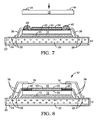
- FIG. 7 is a cross sectional side elevation view into a semiconductor package with stacked dies made in accordance with a third exemplary embodiment of the present invention, before a second, top die is mounted to the top of a first, bottom die;
- FIG. 8 is a cross sectional side elevation view into the package illustrated in FIG. 7 after the second die is mounted to the top surface of the first die;
- FIG. 9 is a top plan view of a portion of the first and second exemplary embodiments illustrated in FIGS. 4 and 6, respectively, after the attachment of the second die to the first die; and,
- the first embodiment of the package 10 shown includes a conventional laminate-type substrate 12 comprising an insulative layer 20 sandwiched between top and bottom layers 22 , 24 of a metal, e.g., copper or aluminum.
- a metal e.g., copper or aluminum.
- a lead-frame-type of substrate can be substituted for the laminate-type substrate illustrated.
- a first semiconductor die 14 is provided which has opposite top and bottom surfaces and a plurality of wire bonding pads 34 located around the periphery of the top surface thereof.
- the bottom surface of the first die 14 is attached to a top surface of the substrate 12 with, e.g., an adhesive tape or a layer of an adhesive 13 , in a conventional manner, which may be effected with automated die-attach apparatus of a type known in the industry.
- a second semiconductor die 16 is provided having opposite top and bottom surfaces, and a plurality of wire bonding pads 34 located around the periphery of the top surface thereof.
- the length and width of the second die 16 are respectively equal to the length and width of the first die 14 , as would be the case where the two dies are identical to one another, e.g., the dies in a memory device.
- the second die 16 is attached to the top surface of the first die 14 by pressing its bottom surface down onto the adhesive 40 in the direction of the arrow shown therein, which has the effect of squeezing, or distributing, the adhesive radially outward from the center of the two opposing die surfaces in a generally rectangular pattern, as shown in FIG. 9 .
- the second die 16 is pressed down onto the adhesive 40 until a desired bond line thickness and lateral extent of the adhesive are obtained.
- the resulting bond line thickness is such that the bottom surface of the second die is spaced apart from the top surface of the first die 14 by a layer 42 of the adhesive 40 thick enough to prevent the bottom surface of the second die from contacting any of the first plurality of conductive wires 38 extending over the top surface of the first die 14 ; and 2) the radial extent of the layer 42 of adhesive 40 is such that it covers substantially all of the top surface of the first die 14 and the bottom surface of the second die 16 , including the bonding pads 34 on the top surface of the first die 14 and the inner ends of the first plurality of conductive wires 38 bonded thereto.
- the adhesive 40 will typically reach the middle 44 of the edges of the dies 14 and 16 before it reaches their corners 46 .
- the upper die 16 has wire bonding pads 34 located at its corners, it is necessary to express the adhesive 40 until the adhesive layer 42 reaches the spaces below the corners 46 of the die, i.e., until substantially all of the upper die 16 is supported by the layer of adhesive.
- the adhesive 40 When the adhesive 40 has been distributed between the two opposing surfaces of the dies 14 and 16 as above, the adhesive is cured to solidify it, which, depending on the type of adhesive employed, may be effected by, e.g., heating the adhesive, or irradiating it with ultra-violet (“U.V.”) light.
- U.V. ultra-violet
- the wire bonding pads 34 on the top surface of the second die 16 may be safely wire bonded to the wire bonding areas 26 on the top surface of the substrate 12 with a second plurality of conductive wires 38 (see FIG.
- the second die 16 is then simply pressed down onto the filled adhesive 40 until the bottom surface of the second die “bottoms out” on the microspheres 48 , i.e., is spaced apart from the top surface of the first die 14 by a single layer of the microspheres.
- the cured layer 42 of the filled adhesive 40 extend below each of the wire bonding pads 34 on the top surface of the second die 16 to achieve the desired support of the second die 16 .
- the cured layer 42 of adhesive 40 extend laterally to the edges 44 of the opposing surfaces of the two dies 14 and 16 so that molded encapsulant of the body 60 cannot flow into the peripheral space 19 between the dies and create a potential “thermal wedge” therein.
- the material of the microspheres 48 can be selected such that they maintain their spherical nature regardless of the curing processes applied to the adhesive 40 matrix in which they are incorporated, e.g., glass, silicon dioxide, silicon nitride, or polytetraflouroethylene (Teflon) microspheres.
- Other materials can be selected that cause the microspheres to become integrally “homogenized” into the fluid adhesive 40 matrix when the latter cures, e.g., a thermoplastic polymer that melts at the same temperature at which a thermo-curing adhesive is cured.
- the microspheres 48 can be fabricated from a variety of suitable materials using a variety of known techniques, e.g., by pumping or blowing a molten material through a nozzle under high pressure to atomize it, then cooling or curing the varying-sized spherical bodies thereby produced with a bath of, e.g., air, water or oil.
- the microspheres 48 can then be passed through a series of screens of graduated mesh sizes to grade them by diameter.
- the third embodiment comprises interposing a spacer 50 between the top surface of the first die 14 and the bottom surface of the second die 16 .
- the spacer 50 has opposite top and bottom surfaces, each with a respective layer 54 and 52 of an adhesive thereon, an overall thickness equal to the desired final thickness of the layer 42 of adhesive 40 between the first and second dies 14 and 16 , and a perimeter 17 (shown as a dotted line in FIG. 10) positioned inside of the wire bonding pads 34 on the top surface of the first die 14 .
- the first die 14 is conventionally attached to the substrate 12 with a layer of adhesive or double-backed adhesive tape 13 , as in the first and second embodiments above, then wire bonded to the substrate with a first plurality of conductive wires 38 .
- the spacer 50 is then attached to the top surface of the first die 14 with the layer of adhesive 52 , such that the perimeter 17 of the spacer is positioned inside of the wire bonding pads 34 on the top surface of the first die.
- a bead of uncured, fluid adhesive 40 is dispensed onto the top surface of the first die 14 outside of and completely around the perimeter 17 of the spacer 50 , and the second die 16 is pressed down onto the first die until its bottom surface contacts the layer 54 of adhesive on the top surface of the spacer 50 .
- the pressure of the second die 16 on the fluid adhesive 40 forces the adhesive outward from spacer 50 and toward the edges 44 of the two dies in a generally rectangular pattern, as illustrated in the plan view of FIG. 10, and the second die is pressed down until its bottom surface is spaced apart from the top surface of the first die 14 by the thickness of the spacer.
- the adhesive 40 covers the wire bonding pads 34 on the top surface of the first die 14 and the connections of the first plurality of bonding wires to those pads, and substantially fills the peripheral space between the two dies.
- the adhesive 40 thus covers the entire area of the respective top and bottom surfaces of the first and second dies 14 and 16 that are not already covered by the spacer 50 , thereby excluding the encapsulant of the package body 60 (see FIG. 2) from the space 19 between the stacked dies.
- the spacer 50 can be made from a variety of materials, including a fiberglass matrix impregnated with a tacky, uncured (i.e., “B-stage”) epoxy resin, or a ceramic, silicon or an oxide thereof, or alternatively, a plastic polymer sheet cut to the appropriate size.
- the adhesive layers 52 and 54 can be applied to the spacer 50 before it is attached to the first die 14 , or alternatively, can be applied sequentially at the time the spacer is mounted to the die, first to the top surface of the first die 14 , then to the top surface of the spacer before the second die is mounted on top of it.
- the adhesive layer 54 used to mount the second die 16 on the spacer 50 can comprise the same adhesive material as the bead of uncured, fluid adhesive 40 dispensed around the perimeter 17 of the spacer 50 , and can be deposited simultaneously therewith. In all cases, the layers of adhesive 52 and 54 on the spacer 50 , and the layer 42 of adhesive 40 may all be simultaneously cured in a single step.
- FIG. 1 Another embodiment within scope of the present invention is a hybrid between the prior art package 10 of FIG. 1 and the second exemplary package 10 embodiment illustrated in FIGS. 5 and 6.
- a layer 42 of adhesive containing microspheres 48 is dispensed onto the top surface of the first die 14 , but is applied such that, upon stacking the second die 16 thereon and curing the adhesive to harden it, the adhesive layer 42 is laterally confined entirely within the wire bonding pads 34 on the top surface of the first die 14 .
- This embodiment has the advantage of a controlled bond line thickness between the dies 14 and 16 , which spaces the second die 16 above the bottom die 14 so that the conductive wires 38 bonded to the first die 14 are not contacted by the second die 16 .
- the second die 16 may be equal in size to the first die 14 , or may have a length and/or a width that are respectively larger than the length and/or width of the first die 14 , although such an embodiment would also be proportionately more susceptible to the “cantilever” problem than one in which the dies are the same size.
Abstract
Description
Claims (27)
Priority Applications (2)
| Application Number | Priority Date | Filing Date | Title |
|---|---|---|---|
| US09/620,444 US6472758B1 (en) | 2000-07-20 | 2000-07-20 | Semiconductor package including stacked semiconductor dies and bond wires |
| US10/224,864 US6650019B2 (en) | 2000-07-20 | 2002-08-20 | Method of making a semiconductor package including stacked semiconductor dies |
Applications Claiming Priority (1)
| Application Number | Priority Date | Filing Date | Title |
|---|---|---|---|
| US09/620,444 US6472758B1 (en) | 2000-07-20 | 2000-07-20 | Semiconductor package including stacked semiconductor dies and bond wires |
Related Child Applications (1)
| Application Number | Title | Priority Date | Filing Date |
|---|---|---|---|
| US10/224,864 Division US6650019B2 (en) | 2000-07-20 | 2002-08-20 | Method of making a semiconductor package including stacked semiconductor dies |
Publications (1)
| Publication Number | Publication Date |
|---|---|
| US6472758B1 true US6472758B1 (en) | 2002-10-29 |
Family
ID=24485967
Family Applications (2)
| Application Number | Title | Priority Date | Filing Date |
|---|---|---|---|
| US09/620,444 Expired - Lifetime US6472758B1 (en) | 2000-07-20 | 2000-07-20 | Semiconductor package including stacked semiconductor dies and bond wires |
| US10/224,864 Expired - Lifetime US6650019B2 (en) | 2000-07-20 | 2002-08-20 | Method of making a semiconductor package including stacked semiconductor dies |
Family Applications After (1)
| Application Number | Title | Priority Date | Filing Date |
|---|---|---|---|
| US10/224,864 Expired - Lifetime US6650019B2 (en) | 2000-07-20 | 2002-08-20 | Method of making a semiconductor package including stacked semiconductor dies |
Country Status (1)
| Country | Link |
|---|---|
| US (2) | US6472758B1 (en) |
Cited By (84)
| Publication number | Priority date | Publication date | Assignee | Title |
|---|---|---|---|---|
| US20020131258A1 (en) * | 2001-03-14 | 2002-09-19 | Murata Manufacturing Co., Ltd. | Mounting structure for module substrates |
| US20030038355A1 (en) * | 2001-08-24 | 2003-02-27 | Derderian James M. | Semiconductor devices and semiconductor device assemblies including a nonconfluent spacer layer |
| US6593662B1 (en) * | 2000-06-16 | 2003-07-15 | Siliconware Precision Industries Co., Ltd. | Stacked-die package structure |
| US20030148597A1 (en) * | 2002-01-09 | 2003-08-07 | Tan Hock Chuan | Stacked die in die BGA package |
| US20030173679A1 (en) * | 2002-03-13 | 2003-09-18 | Levardo Melvin N. | Stacked dice standoffs |
| US20030178710A1 (en) * | 2002-03-21 | 2003-09-25 | Samsung Electronics Co., Ltd. | Semiconductor chip stack structure and method for forming the same |
| US20030189259A1 (en) * | 2002-04-05 | 2003-10-09 | Nec Electronics Corporation | Semiconductor device and method for manufacturing the same |
| US20040007782A1 (en) * | 2002-05-15 | 2004-01-15 | Harry Hedler | Connecting circuit devices and assemblies thereof |
| US20040016939A1 (en) * | 2002-07-26 | 2004-01-29 | Masayuki Akiba | Encapsulation of a stack of semiconductor dice |
| US20040038449A1 (en) * | 2000-08-23 | 2004-02-26 | Corisis David J. | Stacked microelectronic dies and methods for stacking microelectronic dies |
| US20040095736A1 (en) * | 2002-11-18 | 2004-05-20 | Samsung Electronics Co., Ltd. | Multi-chip package having increased reliabilty |
| US6798931B2 (en) * | 2001-03-06 | 2004-09-28 | Digital Optics Corp. | Separating of optical integrated modules and structures formed thereby |
| US6806309B2 (en) | 2002-02-28 | 2004-10-19 | Henkel Corporation | Adhesive compositions containing organic spacers and methods for use thereof |
| US20040224481A1 (en) * | 2003-02-24 | 2004-11-11 | Seiko Epson Corporation | Semiconductor devices, manufacturing methods therefor, circuit substrates and electronic devices |
| US20040251526A1 (en) * | 2003-06-16 | 2004-12-16 | St Assembly Test Services Ltd. | System for semiconductor package with stacked dies |
| US20050001330A1 (en) * | 2003-07-01 | 2005-01-06 | Stmicroelectronics, Inc. | System and method for controlling integrated circuit die height and planarity |
| US20050019984A1 (en) * | 2000-08-09 | 2005-01-27 | Tongbi Jiang | Multiple substrate microelectronic devices and methods of manufacture |
| US6861288B2 (en) | 2003-01-23 | 2005-03-01 | St Assembly Test Services, Ltd. | Stacked semiconductor packages and method for the fabrication thereof |
| US20050048698A1 (en) * | 2003-07-31 | 2005-03-03 | Seiko Epson Corporation | Semiconductor device, method for manufacturing the same, circuit board, and electronic apparatus |
| US20050078436A1 (en) * | 2002-03-20 | 2005-04-14 | Sturcken Keith K. | Method for stacking chips within a multichip module package |
| US20050110126A1 (en) * | 2003-11-25 | 2005-05-26 | Kai-Chiang Wu | Chip adhesive |
| US20050196941A1 (en) * | 2004-03-02 | 2005-09-08 | Chippac, Inc. | DBG system and method with adhesive layer severing |
| US20050208701A1 (en) * | 2004-03-02 | 2005-09-22 | Chippac, Inc. | Semiconductor chip packaging method with individually placed film adhesive pieces |
| US20050208700A1 (en) * | 2004-03-19 | 2005-09-22 | Chippac, Inc. | Die to substrate attach using printed adhesive |
| US20050218479A1 (en) * | 2004-04-01 | 2005-10-06 | Chippac, Inc. | Spacer die structure and method for attaching |
| US20050224959A1 (en) * | 2004-04-01 | 2005-10-13 | Chippac, Inc | Die with discrete spacers and die spacing method |
| US20050224919A1 (en) * | 2004-04-01 | 2005-10-13 | Chippac, Inc | Spacer die structure and method for attaching |
| US20050248019A1 (en) * | 2004-05-10 | 2005-11-10 | Te-Tsung Chao | Overhang support for a stacked semiconductor device, and method of forming thereof |
| US20050258545A1 (en) * | 2004-05-24 | 2005-11-24 | Chippac, Inc. | Multiple die package with adhesive/spacer structure and insulated die surface |
| US20050269676A1 (en) * | 2004-05-24 | 2005-12-08 | Chippac, Inc | Adhesive/spacer island structure for stacking over wire bonded die |
| US20060022323A1 (en) * | 2004-07-29 | 2006-02-02 | Swee Seng Eric T | Assemblies including stacked semiconductor dice having centrally located, wire bonded bond pads |
| US7023096B2 (en) * | 2001-09-28 | 2006-04-04 | Samsung Electronics Co., Ltd. | Multi-chip package having spacer that is inserted between chips and manufacturing method thereof |
| US20060202319A1 (en) * | 2004-08-19 | 2006-09-14 | Swee Seng Eric T | Assemblies and multi-chip modules including stacked semiconductor dice having centrally located, wire bonded bond pads |
| US20060249829A1 (en) * | 2005-04-08 | 2006-11-09 | Mitsuaki Katagiri | Stacked type semiconductor device |
| US20060258044A1 (en) * | 2005-05-11 | 2006-11-16 | Infineon Technologies Ag | Method of manufacturing a semiconductor device comprising stacked chips and a corresponding semiconductor device |
| US20060270112A1 (en) * | 2004-06-30 | 2006-11-30 | Te-Tsung Chao | Overhang support for a stacked semiconductor device, and method of forming thereof |
| US20070015314A1 (en) * | 2004-05-24 | 2007-01-18 | Chippac, Inc | Adhesive/Spacer Island Structure for Multiple Die Package |
| US20070023875A1 (en) * | 2005-07-26 | 2007-02-01 | Kabushiki Kaisha Toshiba | Semiconductor package and manufacturing method thereof |
| US20070178666A1 (en) * | 2006-01-31 | 2007-08-02 | Stats Chippac Ltd. | Integrated circuit system with waferscale spacer system |
| US20070181992A1 (en) * | 2006-02-06 | 2007-08-09 | Micron Technology, Inc. | Microelectronic devices and methods for manufacturing microelectronic devices |
| US20070181998A1 (en) * | 2006-02-03 | 2007-08-09 | Stats Chippac Ltd. | Stacked integrated circuit package system with face to face stack configuration |
| US20070194415A1 (en) * | 2006-02-20 | 2007-08-23 | Seng Eric T S | Semiconductor device assemblies including face-to-face semiconductor dice, systems including such assemblies, and methods for fabricating such assemblies |
| US20070200216A1 (en) * | 2004-06-18 | 2007-08-30 | Samsung Electronics Co., Ltd. | Chip stack package |
| US20070231970A1 (en) * | 2006-03-31 | 2007-10-04 | Tsuyoshi Fukuo | Cured mold compound spacer for stacked-die package |
| US20070229107A1 (en) * | 2006-04-01 | 2007-10-04 | Stats Chippac Ltd. | Stacked integrated circuit package system with connection protection |
| US20070296086A1 (en) * | 2006-06-12 | 2007-12-27 | Jong Wook Ju | Integrated circuit package system with offset stack |
| US20080012095A1 (en) * | 2006-07-11 | 2008-01-17 | Stats Chippac Ltd. | Integrated circuit package system including wafer level spacer |
| US20080042245A1 (en) * | 2006-08-18 | 2008-02-21 | Stats Chippac Ltd. | Integrated circuit package system with waferscale spacer |
| US20080054432A1 (en) * | 2006-09-01 | 2008-03-06 | Corisis David J | High density stacked die assemblies, structures incorporated therein and methods of fabricating the assemblies |
| US20080057624A1 (en) * | 2005-09-07 | 2008-03-06 | Lee Dae W | Stack type semiconductor package utilizing solder coated stacking protrusions and method for manufacturing the same |
| US20080150120A1 (en) * | 2005-08-24 | 2008-06-26 | Fujitsu Limited | Semiconductor device and method of producing the same |
| US20080197509A1 (en) * | 2007-02-15 | 2008-08-21 | Elpida Memory, Inc. | Semiconductor package having stacked semiconductor chips |
| US20080237824A1 (en) * | 2006-02-17 | 2008-10-02 | Amkor Technology, Inc. | Stacked electronic component package having single-sided film spacer |
| US20080251707A1 (en) * | 2001-10-23 | 2008-10-16 | Tessera North America | Optical chassis, camera having an optical chassis, and associated methods |
| US20080308915A1 (en) * | 2006-03-17 | 2008-12-18 | Chipmos Technologies Inc. | Chip package |
| US20090001612A1 (en) * | 2007-06-26 | 2009-01-01 | Sungmin Song | Integrated circuit package system with dual side connection |
| US20090014893A1 (en) * | 2007-07-10 | 2009-01-15 | Jonathan Abela | Integrated circuit package system with wire-in-film isolation barrier |
| US20090020893A1 (en) * | 2007-07-16 | 2009-01-22 | Taeg Ki Lim | Integrated circuit package system with triple film spacer |
| US20090091042A1 (en) * | 2007-10-04 | 2009-04-09 | Byung Tai Do | Integrated circuit package system including die having relieved active region |
| US20090189275A1 (en) * | 2008-01-30 | 2009-07-30 | Ko Wonjun | Integrated circuit package system with wafer scale heat slug |
| US20090223937A1 (en) * | 2008-03-10 | 2009-09-10 | Micron Technology, Inc. | Apparatus and methods for forming wire bonds |
| US7675180B1 (en) * | 2006-02-17 | 2010-03-09 | Amkor Technology, Inc. | Stacked electronic component package having film-on-wire spacer |
| US7723852B1 (en) * | 2008-01-21 | 2010-05-25 | Amkor Technology, Inc. | Stacked semiconductor package and method of making same |
| US20100143722A1 (en) * | 2008-12-05 | 2010-06-10 | Anderson David M | Bond line control process |
| US20100227117A1 (en) * | 2009-03-09 | 2010-09-09 | The Boeing Company | Tapered patch for predictable bonded rework of composite structures |
| US20100227106A1 (en) * | 2009-03-09 | 2010-09-09 | The Boeing Company | Predictable bonded rework of composite structures using tailored patches |
| US20100227105A1 (en) * | 2009-03-09 | 2010-09-09 | The Boeing Company | Predictable bonded rework of composite structures |
| US20100233424A1 (en) * | 2009-03-10 | 2010-09-16 | The Boeing Company | Composite structures employing quasi-isotropic laminates |
| US20100276064A1 (en) * | 2008-12-05 | 2010-11-04 | The Boeing Company | Bonded patches with bond line control |
| US20100276065A1 (en) * | 2008-12-05 | 2010-11-04 | The Boeing Company | Bonded Patches With Bond Line Control |
| US7829986B2 (en) | 2006-04-01 | 2010-11-09 | Stats Chippac Ltd. | Integrated circuit package system with net spacer |
| US7863723B2 (en) | 2001-03-09 | 2011-01-04 | Amkor Technology, Inc. | Adhesive on wire stacked semiconductor package |
| US8030134B2 (en) | 2004-05-24 | 2011-10-04 | Chippac, Inc. | Stacked semiconductor package having adhesive/spacer structure and insulation |
| US8101459B2 (en) * | 2001-08-24 | 2012-01-24 | Micron Technology, Inc. | Methods for assembling semiconductor devices in stacked arrangements by positioning spacers therebetween |
| US8129849B1 (en) | 2006-05-24 | 2012-03-06 | Amkor Technology, Inc. | Method of making semiconductor package with adhering portion |
| WO2012034052A1 (en) * | 2010-09-09 | 2012-03-15 | Advanced Micro Devices, Inc. | Semiconductor chip device with polymeric filler trench |
| US8233757B2 (en) | 2001-10-23 | 2012-07-31 | Digitaloptics Corporation East | Wafer based optical chassis and associated methods |
| US8468709B2 (en) | 2010-11-04 | 2013-06-25 | The Boeing Company | Quick composite repair template tool and method |
| US8524356B1 (en) | 2009-03-09 | 2013-09-03 | The Boeing Company | Bonded patch having multiple zones of fracture toughness |
| US8617694B1 (en) | 2009-03-09 | 2013-12-31 | The Boeing Company | Discretely tailored multi-zone bondline for fail-safe structural repair |
| US9492975B2 (en) | 2009-03-09 | 2016-11-15 | The Boeing Company | Structural bonded patch with tapered adhesive design |
| US20170301598A1 (en) * | 2005-08-19 | 2017-10-19 | Micron Technology, Inc. | Microelectronic devices, stacked microelectronic devices, and methods for manufacturing microelectronic devices |
| US10022922B2 (en) | 2008-12-05 | 2018-07-17 | The Boeing Company | Bonded patches with bond line control |
| US10325863B2 (en) * | 2017-02-28 | 2019-06-18 | Kabushiki Kaisha Toshiba | Semiconductor device and method for manufacturing same |
Families Citing this family (54)
| Publication number | Priority date | Publication date | Assignee | Title |
|---|---|---|---|---|
| US6781225B2 (en) * | 2000-09-15 | 2004-08-24 | Chipmos Technologies Inc. | Glueless integrated circuit system in a packaging module |
| US20020096761A1 (en) * | 2001-01-24 | 2002-07-25 | Chen Wen Chuan | Structure of stacked integrated circuits and method for manufacturing the same |
| US6777648B2 (en) * | 2002-01-11 | 2004-08-17 | Intel Corporation | Method and system to manufacture stacked chip devices |
| US6885093B2 (en) * | 2002-02-28 | 2005-04-26 | Freescale Semiconductor, Inc. | Stacked die semiconductor device |
| KR100472286B1 (en) * | 2002-09-13 | 2005-03-10 | 삼성전자주식회사 | Semiconductor chip package that adhesive tape is attached on the bonding wire |
| US7053476B2 (en) * | 2002-09-17 | 2006-05-30 | Chippac, Inc. | Semiconductor multi-package module having package stacked over die-down flip chip ball grid array package and having wire bond interconnect between stacked packages |
| US7064426B2 (en) * | 2002-09-17 | 2006-06-20 | Chippac, Inc. | Semiconductor multi-package module having wire bond interconnect between stacked packages |
| US20040061213A1 (en) * | 2002-09-17 | 2004-04-01 | Chippac, Inc. | Semiconductor multi-package module having package stacked over die-up flip chip ball grid array package and having wire bond interconnect between stacked packages |
| US7049691B2 (en) | 2002-10-08 | 2006-05-23 | Chippac, Inc. | Semiconductor multi-package module having inverted second package and including additional die or stacked package on second package |
| US7034387B2 (en) | 2003-04-04 | 2006-04-25 | Chippac, Inc. | Semiconductor multipackage module including processor and memory package assemblies |
| TWI242274B (en) * | 2003-02-27 | 2005-10-21 | Siliconware Precision Industries Co Ltd | Ball grid array semiconductor package and method for fabricating the same |
| JP2004281634A (en) * | 2003-03-14 | 2004-10-07 | Renesas Technology Corp | Method for manufacturing stacked package semiconductor device |
| US6885108B2 (en) * | 2003-03-18 | 2005-04-26 | Micron Technology, Inc. | Protective layers formed on semiconductor device components so as to reduce or eliminate the occurrence of delamination thereof and cracking therein |
| US6793500B1 (en) * | 2003-09-18 | 2004-09-21 | International Business Machines Corporation | Radial contact pad footprint and wiring for electrical components |
| JP5197961B2 (en) | 2003-12-17 | 2013-05-15 | スタッツ・チップパック・インコーポレイテッド | Multi-chip package module and manufacturing method thereof |
| TWI237882B (en) * | 2004-05-11 | 2005-08-11 | Via Tech Inc | Stacked multi-chip package |
| WO2005117092A2 (en) * | 2004-05-24 | 2005-12-08 | Chippac, Inc. | Stacked semiconductor package having adhesive/spacer structure and insulation |
| US7202105B2 (en) * | 2004-06-28 | 2007-04-10 | Semiconductor Components Industries, L.L.C. | Multi-chip semiconductor connector assembly method |
| US7202106B2 (en) * | 2004-06-28 | 2007-04-10 | Semiconductor Components Industries, L.L.C. | Multi-chip semiconductor connector and method |
| US7298034B2 (en) * | 2004-06-28 | 2007-11-20 | Semiconductor Components Industries, L.L.C. | Multi-chip semiconductor connector assemblies |
| US7253511B2 (en) | 2004-07-13 | 2007-08-07 | Chippac, Inc. | Semiconductor multipackage module including die and inverted land grid array package stacked over ball grid array package |
| KR100639701B1 (en) * | 2004-11-17 | 2006-10-30 | 삼성전자주식회사 | Multi chip package |
| EP1688997B1 (en) * | 2005-02-02 | 2014-04-16 | Infineon Technologies AG | Electronic component with stacked semiconductor chips |
| US7364945B2 (en) | 2005-03-31 | 2008-04-29 | Stats Chippac Ltd. | Method of mounting an integrated circuit package in an encapsulant cavity |
| JP5346578B2 (en) | 2005-03-31 | 2013-11-20 | スタッツ・チップパック・リミテッド | Semiconductor assembly and manufacturing method thereof |
| TWI423401B (en) | 2005-03-31 | 2014-01-11 | Stats Chippac Ltd | Semiconductor stacked package assembly having exposed substrate surfaces on upper and lower sides |
| US7354800B2 (en) | 2005-04-29 | 2008-04-08 | Stats Chippac Ltd. | Method of fabricating a stacked integrated circuit package system |
| US7429786B2 (en) | 2005-04-29 | 2008-09-30 | Stats Chippac Ltd. | Semiconductor package including second substrate and having exposed substrate surfaces on upper and lower sides |
| US7582960B2 (en) | 2005-05-05 | 2009-09-01 | Stats Chippac Ltd. | Multiple chip package module including die stacked over encapsulated package |
| US7394148B2 (en) | 2005-06-20 | 2008-07-01 | Stats Chippac Ltd. | Module having stacked chip scale semiconductor packages |
| US20070109831A1 (en) * | 2005-11-15 | 2007-05-17 | Siva Raghuram | Semiconductor product and method for forming a semiconductor product |
| US7456088B2 (en) | 2006-01-04 | 2008-11-25 | Stats Chippac Ltd. | Integrated circuit package system including stacked die |
| US7768125B2 (en) | 2006-01-04 | 2010-08-03 | Stats Chippac Ltd. | Multi-chip package system |
| US7750482B2 (en) | 2006-02-09 | 2010-07-06 | Stats Chippac Ltd. | Integrated circuit package system including zero fillet resin |
| US8704349B2 (en) | 2006-02-14 | 2014-04-22 | Stats Chippac Ltd. | Integrated circuit package system with exposed interconnects |
| US7993969B2 (en) * | 2006-08-10 | 2011-08-09 | Infineon Technologies Ag | Method for producing a module with components stacked one above another |
| US20080054429A1 (en) * | 2006-08-25 | 2008-03-06 | Bolken Todd O | Spacers for separating components of semiconductor device assemblies, semiconductor device assemblies and systems including spacers and methods of making spacers |
| US20080131998A1 (en) * | 2006-12-01 | 2008-06-05 | Hem Takiar | Method of fabricating a film-on-wire bond semiconductor device |
| US20080128879A1 (en) * | 2006-12-01 | 2008-06-05 | Hem Takiar | Film-on-wire bond semiconductor device |
| TWM315922U (en) * | 2006-12-08 | 2007-07-21 | Delta Electronics Inc | Filter device and apparatus |
| US8106491B2 (en) | 2007-05-16 | 2012-01-31 | Micron Technology, Inc. | Methods of forming stacked semiconductor devices with a leadframe and associated assemblies |
| US7678615B2 (en) * | 2007-08-29 | 2010-03-16 | Advanced Micro Devices, Inc. | Semiconductor device with gel-type thermal interface material |
| US7833839B1 (en) * | 2007-09-15 | 2010-11-16 | Globalfoundries Inc. | Method for decreasing surface delamination of gel-type thermal interface material by management of the material cure temperature |
| US9059074B2 (en) * | 2008-03-26 | 2015-06-16 | Stats Chippac Ltd. | Integrated circuit package system with planar interconnect |
| US8923004B2 (en) * | 2008-07-31 | 2014-12-30 | Micron Technology, Inc. | Microelectronic packages with small footprints and associated methods of manufacturing |
| JP4360446B1 (en) * | 2008-10-16 | 2009-11-11 | 住友ベークライト株式会社 | Semiconductor device manufacturing method and semiconductor device |
| MY166609A (en) * | 2010-09-15 | 2018-07-17 | Semiconductor Components Ind Llc | Connector assembly and method of manufacture |
| MY163661A (en) * | 2010-09-15 | 2017-10-13 | Semiconductor Components Ind Llc | Semiconductor component and method of manufacture |
| US8987875B2 (en) * | 2013-03-08 | 2015-03-24 | Delphi Technologies, Inc. | Balanced stress assembly for semiconductor devices |
| US9082868B2 (en) | 2013-03-13 | 2015-07-14 | Semiconductor Components Industries, Llc | Semiconductor component and method of manufacture |
| EP3146560A4 (en) * | 2014-05-23 | 2018-04-18 | Materion Corporation | Air cavity package |
| US9305901B2 (en) * | 2014-07-17 | 2016-04-05 | Seagate Technology Llc | Non-circular die package interconnect |
| US10921536B2 (en) * | 2017-05-18 | 2021-02-16 | Arista Networks, Inc. | Heat sink for optical transceiver |
| US20230178457A1 (en) * | 2021-12-08 | 2023-06-08 | Nxp B.V. | Semiconductor package having lead frame with semiconductor die and component module mounted on opposite surfaces of the lead frame and methods of manufacture thereof |
Citations (52)
| Publication number | Priority date | Publication date | Assignee | Title |
|---|---|---|---|---|
| US3851221A (en) | 1972-11-30 | 1974-11-26 | P Beaulieu | Integrated circuit package |
| US4103318A (en) | 1977-05-06 | 1978-07-25 | Ford Motor Company | Electronic multichip module |
| US4361261A (en) | 1978-11-22 | 1982-11-30 | Kulicke & Soffa Industries, Inc. | Apparatus for wire bonding |
| US4444349A (en) | 1981-05-04 | 1984-04-24 | Kulicke & Soffa Industries, Inc. | Wire bonding apparatus |
| JPS6159862A (en) | 1984-08-31 | 1986-03-27 | Fujitsu Ltd | Semiconductor device |
| US4586642A (en) | 1985-05-13 | 1986-05-06 | Kulicke And Soffa Industries Inc. | Wire bond monitoring system |
| JPS61117858A (en) | 1984-11-14 | 1986-06-05 | Hitachi Micro Comput Eng Ltd | Semiconductor device |
| JPS62119952A (en) | 1985-11-19 | 1987-06-01 | Nec Corp | Integrated circuit device |
| JPS62126661A (en) | 1985-11-27 | 1987-06-08 | Nec Corp | Hybrid integrated circuit device |
| JPS62142341A (en) | 1985-12-17 | 1987-06-25 | Matsushita Electronics Corp | Semiconductor device and manufacture thereof |
| US4730232A (en) | 1986-06-25 | 1988-03-08 | Westinghouse Electric Corp. | High density microelectronic packaging module for high speed chips |
| JPS63128736A (en) | 1986-11-19 | 1988-06-01 | Olympus Optical Co Ltd | Semiconductor element |
| US4763188A (en) | 1986-08-08 | 1988-08-09 | Thomas Johnson | Packaging system for multiple semiconductor devices |
| JPS63211663A (en) | 1987-02-26 | 1988-09-02 | Mitsubishi Electric Corp | Circuit board |
| JPS63244654A (en) | 1987-03-31 | 1988-10-12 | Toshiba Corp | Plastic molded type integrated circuit device |
| JPH0199248A (en) | 1987-10-13 | 1989-04-18 | Mitsubishi Electric Corp | Semiconductor device |
| US4862322A (en) * | 1988-05-02 | 1989-08-29 | Bickford Harry R | Double electronic device structure having beam leads solderlessly bonded between contact locations on each device and projecting outwardly from therebetween |
| US4982265A (en) | 1987-06-24 | 1991-01-01 | Hitachi, Ltd. | Semiconductor integrated circuit device and method of manufacturing the same |
| US5025306A (en) | 1988-08-09 | 1991-06-18 | Texas Instruments Incorporated | Assembly of semiconductor chips |
| US5040052A (en) | 1987-12-28 | 1991-08-13 | Texas Instruments Incorporated | Compact silicon module for high density integrated circuits |
| JPH0428260A (en) | 1990-05-23 | 1992-01-30 | Matsushita Electric Ind Co Ltd | Method of mounting semiconductor chip |
| JPH0456262A (en) | 1990-06-25 | 1992-02-24 | Matsushita Electron Corp | Semiconductor integrated circuit device |
| US5140404A (en) | 1990-10-24 | 1992-08-18 | Micron Technology, Inc. | Semiconductor device manufactured by a method for attaching a semiconductor die to a leadframe using a thermoplastic covered carrier tape |
| US5172215A (en) | 1990-03-06 | 1992-12-15 | Fuji Electric Co., Ltd. | Overcurrent-limiting type semiconductor device |
| US5177032A (en) | 1990-10-24 | 1993-01-05 | Micron Technology, Inc. | Method for attaching a semiconductor die to a leadframe using a thermoplastic covered carrier tape |
| US5176311A (en) | 1991-03-04 | 1993-01-05 | Kulicke And Soffa Investments, Inc. | High yield clampless wire bonding method |
| US5291060A (en) | 1989-10-16 | 1994-03-01 | Shinko Electric Industries Co., Ltd. | Lead frame and semiconductor device using same |
| US5291061A (en) | 1993-04-06 | 1994-03-01 | Micron Semiconductor, Inc. | Multi-chip stacked devices |
| US5323060A (en) | 1993-06-02 | 1994-06-21 | Micron Semiconductor, Inc. | Multichip module having a stacked chip arrangement |
| US5384689A (en) | 1993-12-20 | 1995-01-24 | Shen; Ming-Tung | Integrated circuit chip including superimposed upper and lower printed circuit boards |
| US5432729A (en) | 1993-04-23 | 1995-07-11 | Irvine Sensors Corporation | Electronic module comprising a stack of IC chips each interacting with an IC chip secured to the stack |
| US5438224A (en) * | 1992-04-23 | 1995-08-01 | Motorola, Inc. | Integrated circuit package having a face-to-face IC chip arrangement |
| US5620928A (en) | 1995-05-11 | 1997-04-15 | National Semiconductor Corporation | Ultra thin ball grid array using a flex tape or printed wiring board substrate and method |
| US5682062A (en) | 1995-06-05 | 1997-10-28 | Harris Corporation | System for interconnecting stacked integrated circuits |
| JPH1056470A (en) | 1996-08-07 | 1998-02-24 | Oki Electric Ind Co Ltd | Network communication control equipment |
| US5721452A (en) | 1995-08-16 | 1998-02-24 | Micron Technology, Inc. | Angularly offset stacked die multichip device and method of manufacture |
| US5739581A (en) | 1995-11-17 | 1998-04-14 | National Semiconductor Corporation | High density integrated circuit package assembly with a heatsink between stacked dies |
| US5815372A (en) | 1997-03-25 | 1998-09-29 | Intel Corporation | Packaging multiple dies on a ball grid array substrate |
| US5872025A (en) | 1995-07-26 | 1999-02-16 | International Business Machines Corporation | Method for stacked three dimensional device manufacture |
| US5877478A (en) * | 1992-05-14 | 1999-03-02 | Kabushiki Kaisha Toshiba | Semiconductor device and method of manufacturing the same |
| US5886412A (en) | 1995-08-16 | 1999-03-23 | Micron Technology, Inc. | Angularly offset and recessed stacked die multichip device |
| US5989982A (en) | 1997-10-08 | 1999-11-23 | Oki Electric Industry Co., Ltd. | Semiconductor device and method of manufacturing the same |
| US6005778A (en) | 1995-06-15 | 1999-12-21 | Honeywell Inc. | Chip stacking and capacitor mounting arrangement including spacers |
| US6013948A (en) | 1995-11-27 | 2000-01-11 | Micron Technology, Inc. | Stackable chip scale semiconductor package with mating contacts on opposed surfaces |
| US6030855A (en) | 1996-04-30 | 2000-02-29 | International Business Machines Corproation | Self-aligned connector for stacked chip module |
| US6033931A (en) | 1997-08-18 | 2000-03-07 | Texas Instruments Incorporated | Semiconductor device including stacked chips having metal patterned on circuit surface and one edge side of chip |
| US6051886A (en) | 1995-08-16 | 2000-04-18 | Micron Technology, Inc. | Angularly offset stacked die multichip device and method of manufacture |
| US6057598A (en) | 1997-01-31 | 2000-05-02 | Vlsi Technology, Inc. | Face on face flip chip integration |
| US6214432B1 (en) * | 1999-06-02 | 2001-04-10 | Sony Corporation, | Method for controlling the bonding layer thickness in an optical storage apparatus and optical storage apparatus resulting therefrom |
| US6232148B1 (en) * | 1996-06-17 | 2001-05-15 | Micron Technology, Inc. | Method and apparatus leads-between-chips |
| US6239496B1 (en) * | 1999-01-18 | 2001-05-29 | Kabushiki Kaisha Toshiba | Package having very thin semiconductor chip, multichip module assembled by the package, and method for manufacturing the same |
| US6262488B1 (en) * | 1987-06-24 | 2001-07-17 | Hitachi Ltd. | Semiconductor memory module having double-sided memory chip layout |
Family Cites Families (9)
| Publication number | Priority date | Publication date | Assignee | Title |
|---|---|---|---|---|
| US5198888A (en) | 1987-12-28 | 1993-03-30 | Hitachi, Ltd. | Semiconductor stacked device |
| US6130116A (en) | 1996-12-13 | 2000-10-10 | Tessera, Inc. | Method of encapsulating a microelectronic assembly utilizing a barrier |
| US6133637A (en) * | 1997-01-24 | 2000-10-17 | Rohm Co., Ltd. | Semiconductor device having a plurality of semiconductor chips |
| JP3481444B2 (en) | 1998-01-14 | 2003-12-22 | シャープ株式会社 | Semiconductor device and manufacturing method thereof |
| US6049094A (en) | 1998-05-21 | 2000-04-11 | National Semiconductor Corporation | Low stress package assembly for silicon-backed light valves |
| KR100277438B1 (en) * | 1998-05-28 | 2001-02-01 | 윤종용 | Multi Chip Package |
| US6201302B1 (en) * | 1998-12-31 | 2001-03-13 | Sampo Semiconductor Corporation | Semiconductor package having multi-dies |
| JP3765952B2 (en) * | 1999-10-19 | 2006-04-12 | 富士通株式会社 | Semiconductor device |
| US6340846B1 (en) | 2000-12-06 | 2002-01-22 | Amkor Technology, Inc. | Making semiconductor packages with stacked dies and reinforced wire bonds |
-
2000
- 2000-07-20 US US09/620,444 patent/US6472758B1/en not_active Expired - Lifetime
-
2002
- 2002-08-20 US US10/224,864 patent/US6650019B2/en not_active Expired - Lifetime
Patent Citations (53)
| Publication number | Priority date | Publication date | Assignee | Title |
|---|---|---|---|---|
| US3851221A (en) | 1972-11-30 | 1974-11-26 | P Beaulieu | Integrated circuit package |
| US4103318A (en) | 1977-05-06 | 1978-07-25 | Ford Motor Company | Electronic multichip module |
| US4361261A (en) | 1978-11-22 | 1982-11-30 | Kulicke & Soffa Industries, Inc. | Apparatus for wire bonding |
| US4444349A (en) | 1981-05-04 | 1984-04-24 | Kulicke & Soffa Industries, Inc. | Wire bonding apparatus |
| JPS6159862A (en) | 1984-08-31 | 1986-03-27 | Fujitsu Ltd | Semiconductor device |
| JPS61117858A (en) | 1984-11-14 | 1986-06-05 | Hitachi Micro Comput Eng Ltd | Semiconductor device |
| US4586642A (en) | 1985-05-13 | 1986-05-06 | Kulicke And Soffa Industries Inc. | Wire bond monitoring system |
| JPS62119952A (en) | 1985-11-19 | 1987-06-01 | Nec Corp | Integrated circuit device |
| JPS62126661A (en) | 1985-11-27 | 1987-06-08 | Nec Corp | Hybrid integrated circuit device |
| JPS62142341A (en) | 1985-12-17 | 1987-06-25 | Matsushita Electronics Corp | Semiconductor device and manufacture thereof |
| US4730232A (en) | 1986-06-25 | 1988-03-08 | Westinghouse Electric Corp. | High density microelectronic packaging module for high speed chips |
| US4763188A (en) | 1986-08-08 | 1988-08-09 | Thomas Johnson | Packaging system for multiple semiconductor devices |
| JPS63128736A (en) | 1986-11-19 | 1988-06-01 | Olympus Optical Co Ltd | Semiconductor element |
| JPS63211663A (en) | 1987-02-26 | 1988-09-02 | Mitsubishi Electric Corp | Circuit board |
| JPS63244654A (en) | 1987-03-31 | 1988-10-12 | Toshiba Corp | Plastic molded type integrated circuit device |
| US4982265A (en) | 1987-06-24 | 1991-01-01 | Hitachi, Ltd. | Semiconductor integrated circuit device and method of manufacturing the same |
| US6262488B1 (en) * | 1987-06-24 | 2001-07-17 | Hitachi Ltd. | Semiconductor memory module having double-sided memory chip layout |
| JPH0199248A (en) | 1987-10-13 | 1989-04-18 | Mitsubishi Electric Corp | Semiconductor device |
| US5040052A (en) | 1987-12-28 | 1991-08-13 | Texas Instruments Incorporated | Compact silicon module for high density integrated circuits |
| US4862322A (en) * | 1988-05-02 | 1989-08-29 | Bickford Harry R | Double electronic device structure having beam leads solderlessly bonded between contact locations on each device and projecting outwardly from therebetween |
| US5025306A (en) | 1988-08-09 | 1991-06-18 | Texas Instruments Incorporated | Assembly of semiconductor chips |
| US5291060A (en) | 1989-10-16 | 1994-03-01 | Shinko Electric Industries Co., Ltd. | Lead frame and semiconductor device using same |
| US5172215A (en) | 1990-03-06 | 1992-12-15 | Fuji Electric Co., Ltd. | Overcurrent-limiting type semiconductor device |
| JPH0428260A (en) | 1990-05-23 | 1992-01-30 | Matsushita Electric Ind Co Ltd | Method of mounting semiconductor chip |
| JPH0456262A (en) | 1990-06-25 | 1992-02-24 | Matsushita Electron Corp | Semiconductor integrated circuit device |
| US5140404A (en) | 1990-10-24 | 1992-08-18 | Micron Technology, Inc. | Semiconductor device manufactured by a method for attaching a semiconductor die to a leadframe using a thermoplastic covered carrier tape |
| US5177032A (en) | 1990-10-24 | 1993-01-05 | Micron Technology, Inc. | Method for attaching a semiconductor die to a leadframe using a thermoplastic covered carrier tape |
| US5176311A (en) | 1991-03-04 | 1993-01-05 | Kulicke And Soffa Investments, Inc. | High yield clampless wire bonding method |
| US5438224A (en) * | 1992-04-23 | 1995-08-01 | Motorola, Inc. | Integrated circuit package having a face-to-face IC chip arrangement |
| US5877478A (en) * | 1992-05-14 | 1999-03-02 | Kabushiki Kaisha Toshiba | Semiconductor device and method of manufacturing the same |
| US5291061A (en) | 1993-04-06 | 1994-03-01 | Micron Semiconductor, Inc. | Multi-chip stacked devices |
| USRE36613E (en) | 1993-04-06 | 2000-03-14 | Micron Technology, Inc. | Multi-chip stacked devices |
| US5432729A (en) | 1993-04-23 | 1995-07-11 | Irvine Sensors Corporation | Electronic module comprising a stack of IC chips each interacting with an IC chip secured to the stack |
| US5323060A (en) | 1993-06-02 | 1994-06-21 | Micron Semiconductor, Inc. | Multichip module having a stacked chip arrangement |
| US5384689A (en) | 1993-12-20 | 1995-01-24 | Shen; Ming-Tung | Integrated circuit chip including superimposed upper and lower printed circuit boards |
| US5620928A (en) | 1995-05-11 | 1997-04-15 | National Semiconductor Corporation | Ultra thin ball grid array using a flex tape or printed wiring board substrate and method |
| US5682062A (en) | 1995-06-05 | 1997-10-28 | Harris Corporation | System for interconnecting stacked integrated circuits |
| US6005778A (en) | 1995-06-15 | 1999-12-21 | Honeywell Inc. | Chip stacking and capacitor mounting arrangement including spacers |
| US5872025A (en) | 1995-07-26 | 1999-02-16 | International Business Machines Corporation | Method for stacked three dimensional device manufacture |
| US5886412A (en) | 1995-08-16 | 1999-03-23 | Micron Technology, Inc. | Angularly offset and recessed stacked die multichip device |
| US5721452A (en) | 1995-08-16 | 1998-02-24 | Micron Technology, Inc. | Angularly offset stacked die multichip device and method of manufacture |
| US6051886A (en) | 1995-08-16 | 2000-04-18 | Micron Technology, Inc. | Angularly offset stacked die multichip device and method of manufacture |
| US5739581A (en) | 1995-11-17 | 1998-04-14 | National Semiconductor Corporation | High density integrated circuit package assembly with a heatsink between stacked dies |
| US6013948A (en) | 1995-11-27 | 2000-01-11 | Micron Technology, Inc. | Stackable chip scale semiconductor package with mating contacts on opposed surfaces |
| US6030855A (en) | 1996-04-30 | 2000-02-29 | International Business Machines Corproation | Self-aligned connector for stacked chip module |
| US6232148B1 (en) * | 1996-06-17 | 2001-05-15 | Micron Technology, Inc. | Method and apparatus leads-between-chips |
| JPH1056470A (en) | 1996-08-07 | 1998-02-24 | Oki Electric Ind Co Ltd | Network communication control equipment |
| US6057598A (en) | 1997-01-31 | 2000-05-02 | Vlsi Technology, Inc. | Face on face flip chip integration |
| US5815372A (en) | 1997-03-25 | 1998-09-29 | Intel Corporation | Packaging multiple dies on a ball grid array substrate |
| US6033931A (en) | 1997-08-18 | 2000-03-07 | Texas Instruments Incorporated | Semiconductor device including stacked chips having metal patterned on circuit surface and one edge side of chip |
| US5989982A (en) | 1997-10-08 | 1999-11-23 | Oki Electric Industry Co., Ltd. | Semiconductor device and method of manufacturing the same |
| US6239496B1 (en) * | 1999-01-18 | 2001-05-29 | Kabushiki Kaisha Toshiba | Package having very thin semiconductor chip, multichip module assembled by the package, and method for manufacturing the same |
| US6214432B1 (en) * | 1999-06-02 | 2001-04-10 | Sony Corporation, | Method for controlling the bonding layer thickness in an optical storage apparatus and optical storage apparatus resulting therefrom |
Cited By (192)
| Publication number | Priority date | Publication date | Assignee | Title |
|---|---|---|---|---|
| US6593662B1 (en) * | 2000-06-16 | 2003-07-15 | Siliconware Precision Industries Co., Ltd. | Stacked-die package structure |
| US7298031B1 (en) | 2000-08-09 | 2007-11-20 | Micron Technology, Inc. | Multiple substrate microelectronic devices and methods of manufacture |
| US7253025B2 (en) | 2000-08-09 | 2007-08-07 | Micron Technology, Inc. | Multiple substrate microelectronic devices and methods of manufacture |
| US20050019984A1 (en) * | 2000-08-09 | 2005-01-27 | Tongbi Jiang | Multiple substrate microelectronic devices and methods of manufacture |
| US8587109B2 (en) | 2000-08-23 | 2013-11-19 | Micron Technology, Inc. | Stacked microelectronic dies and methods for stacking microelectronic dies |
| US20040038449A1 (en) * | 2000-08-23 | 2004-02-26 | Corisis David J. | Stacked microelectronic dies and methods for stacking microelectronic dies |
| US8067827B2 (en) | 2000-08-23 | 2011-11-29 | Micron Technology, Inc. | Stacked microelectronic device assemblies |
| US7235871B2 (en) * | 2000-08-23 | 2007-06-26 | Micron Technology, Inc. | Stacked microelectronic dies |
| US20070210435A1 (en) * | 2000-08-23 | 2007-09-13 | Micron Technology, Inc. | Stacked microelectronic dies and methods for stacking microelectronic dies |
| US7208771B2 (en) | 2001-03-06 | 2007-04-24 | Digital Optics Corporation | Separating of optical integrated modules and structures formed thereby |
| US20070200132A1 (en) * | 2001-03-06 | 2007-08-30 | Digital Optics Corporation | Electrical connection for optoelectronic devices |
| US20050035463A1 (en) * | 2001-03-06 | 2005-02-17 | Digital Optics Corporation | Separating of optical integrated modules and structures formed thereby |
| US6798931B2 (en) * | 2001-03-06 | 2004-09-28 | Digital Optics Corp. | Separating of optical integrated modules and structures formed thereby |
| US7863723B2 (en) | 2001-03-09 | 2011-01-04 | Amkor Technology, Inc. | Adhesive on wire stacked semiconductor package |
| US8143727B2 (en) | 2001-03-09 | 2012-03-27 | Amkor Technology, Inc. | Adhesive on wire stacked semiconductor package |
| US6801440B2 (en) * | 2001-03-14 | 2004-10-05 | Murata Manufacturing Co., Ltd. | Mounting structure for module substrates |
| US20020131258A1 (en) * | 2001-03-14 | 2002-09-19 | Murata Manufacturing Co., Ltd. | Mounting structure for module substrates |
| US20060035408A1 (en) * | 2001-08-24 | 2006-02-16 | Derderian James M | Methods for designing spacers for use in stacking semiconductor devices or semiconductor device components |
| US7518223B2 (en) * | 2001-08-24 | 2009-04-14 | Micron Technology, Inc. | Semiconductor devices and semiconductor device assemblies including a nonconfluent spacer layer |
| US8101459B2 (en) * | 2001-08-24 | 2012-01-24 | Micron Technology, Inc. | Methods for assembling semiconductor devices in stacked arrangements by positioning spacers therebetween |
| US20030038357A1 (en) * | 2001-08-24 | 2003-02-27 | Derderian James M. | Spacer for semiconductor devices, semiconductor devices and assemblies including the spacer, and methods |
| US20030038355A1 (en) * | 2001-08-24 | 2003-02-27 | Derderian James M. | Semiconductor devices and semiconductor device assemblies including a nonconfluent spacer layer |
| US7023096B2 (en) * | 2001-09-28 | 2006-04-04 | Samsung Electronics Co., Ltd. | Multi-chip package having spacer that is inserted between chips and manufacturing method thereof |
| US8233757B2 (en) | 2001-10-23 | 2012-07-31 | Digitaloptics Corporation East | Wafer based optical chassis and associated methods |
| US7961989B2 (en) | 2001-10-23 | 2011-06-14 | Tessera North America, Inc. | Optical chassis, camera having an optical chassis, and associated methods |
| US20080251707A1 (en) * | 2001-10-23 | 2008-10-16 | Tessera North America | Optical chassis, camera having an optical chassis, and associated methods |
| US7575953B2 (en) | 2002-01-09 | 2009-08-18 | Micron Technology, Inc. | Stacked die with a recess in a die BGA package |
| US7282390B2 (en) | 2002-01-09 | 2007-10-16 | Micron Technology, Inc. | Stacked die-in-die BGA package with die having a recess |
| US20080136045A1 (en) * | 2002-01-09 | 2008-06-12 | Micron Technology, Inc. | Stacked die in die BGA package |
| US20060292746A1 (en) * | 2002-01-09 | 2006-12-28 | Micron Technology, Inc. | Stacked die in die BGA package |
| US7371608B2 (en) * | 2002-01-09 | 2008-05-13 | Micron Technology, Inc. | Method of fabricating a stacked die having a recess in a die BGA package |
| US20060292743A1 (en) * | 2002-01-09 | 2006-12-28 | Micron Technolgoy, Inc. | Stacked die in die BGA package |
| US20080096316A1 (en) * | 2002-01-09 | 2008-04-24 | Micron Technology, Inc. | Stacked Die in Die BGA Package |
| US7358117B2 (en) | 2002-01-09 | 2008-04-15 | Micron Technology, Inc. | Stacked die in die BGA package |
| US7344969B2 (en) | 2002-01-09 | 2008-03-18 | Micron Technology, Inc. | Stacked die in die BGA package |
| US20060292745A1 (en) * | 2002-01-09 | 2006-12-28 | Micron Technology, Inc. | Stacked die in die BGA package |
| US8373277B2 (en) | 2002-01-09 | 2013-02-12 | Micron Technology, Inc. | Stacked die in die BGA package |
| US7332819B2 (en) | 2002-01-09 | 2008-02-19 | Micron Technology, Inc. | Stacked die in die BGA package |
| US7332820B2 (en) | 2002-01-09 | 2008-02-19 | Micron Technology, Inc. | Stacked die in die BGA package |
| US20080032449A1 (en) * | 2002-01-09 | 2008-02-07 | Micron Technology, Inc. | Stacked Die in Die BGA Package |
| US20030148597A1 (en) * | 2002-01-09 | 2003-08-07 | Tan Hock Chuan | Stacked die in die BGA package |
| US20030162325A1 (en) * | 2002-01-09 | 2003-08-28 | Micron Technology, Inc. | Stacked die in die BGA package |
| US7309623B2 (en) | 2002-01-09 | 2007-12-18 | Micron Technology, Inc. | Method of fabricating a stacked die in die BGA package |
| US7799610B2 (en) | 2002-01-09 | 2010-09-21 | Micron Technology, Inc. | Method of fabricating a stacked die having a recess in a die BGA package |
| US20060216864A1 (en) * | 2002-01-09 | 2006-09-28 | Micron Technology, Inc. | Stacked die in die BGA package |
| US20030207515A1 (en) * | 2002-01-09 | 2003-11-06 | Micron Technology, Inc., Boise, Id | Stacked die in die BGA package |
| US20030207516A1 (en) * | 2002-01-09 | 2003-11-06 | Micron Technology, Inc. | Stacked die in die BGA package |
| US7282392B2 (en) | 2002-01-09 | 2007-10-16 | Micron Technology, Inc. | Method of fabricating a stacked die in die BGA package |
| US6806309B2 (en) | 2002-02-28 | 2004-10-19 | Henkel Corporation | Adhesive compositions containing organic spacers and methods for use thereof |
| US20030173679A1 (en) * | 2002-03-13 | 2003-09-18 | Levardo Melvin N. | Stacked dice standoffs |
| US6753613B2 (en) * | 2002-03-13 | 2004-06-22 | Intel Corporation | Stacked dice standoffs |
| US20050078436A1 (en) * | 2002-03-20 | 2005-04-14 | Sturcken Keith K. | Method for stacking chips within a multichip module package |
| US20060049528A1 (en) * | 2002-03-21 | 2006-03-09 | Samsung Electronics Co., Ltd. | Semiconductor chip stack structure and method for forming the same |
| US20030178710A1 (en) * | 2002-03-21 | 2003-09-25 | Samsung Electronics Co., Ltd. | Semiconductor chip stack structure and method for forming the same |
| US6977439B2 (en) * | 2002-03-21 | 2005-12-20 | Samsung Electronics Co., Ltd. | Semiconductor chip stack structure |
| US20030189259A1 (en) * | 2002-04-05 | 2003-10-09 | Nec Electronics Corporation | Semiconductor device and method for manufacturing the same |
| US6930396B2 (en) * | 2002-04-05 | 2005-08-16 | Nec Electronics Corporation | Semiconductor device and method for manufacturing the same |
| US6897088B2 (en) * | 2002-05-15 | 2005-05-24 | Infineon Technologies Ag | Method for connecting circuit devices |
| US20040007782A1 (en) * | 2002-05-15 | 2004-01-15 | Harry Hedler | Connecting circuit devices and assemblies thereof |
| US20050085034A1 (en) * | 2002-07-26 | 2005-04-21 | Masayuki Akiba | Encapsulated stack of dice and support therefor |
| US20040016939A1 (en) * | 2002-07-26 | 2004-01-29 | Masayuki Akiba | Encapsulation of a stack of semiconductor dice |
| US7132739B2 (en) | 2002-07-26 | 2006-11-07 | Intel Corporation | Encapsulated stack of dice and support therefor |
| US7132311B2 (en) * | 2002-07-26 | 2006-11-07 | Intel Corporation | Encapsulation of a stack of semiconductor dice |
| US20040095736A1 (en) * | 2002-11-18 | 2004-05-20 | Samsung Electronics Co., Ltd. | Multi-chip package having increased reliabilty |
| US6861288B2 (en) | 2003-01-23 | 2005-03-01 | St Assembly Test Services, Ltd. | Stacked semiconductor packages and method for the fabrication thereof |
| US20040224481A1 (en) * | 2003-02-24 | 2004-11-11 | Seiko Epson Corporation | Semiconductor devices, manufacturing methods therefor, circuit substrates and electronic devices |
| US20040251526A1 (en) * | 2003-06-16 | 2004-12-16 | St Assembly Test Services Ltd. | System for semiconductor package with stacked dies |
| US6833287B1 (en) * | 2003-06-16 | 2004-12-21 | St Assembly Test Services Inc. | System for semiconductor package with stacked dies |
| US20050001330A1 (en) * | 2003-07-01 | 2005-01-06 | Stmicroelectronics, Inc. | System and method for controlling integrated circuit die height and planarity |
| US7456050B2 (en) * | 2003-07-01 | 2008-11-25 | Stmicroelectronics, Inc. | System and method for controlling integrated circuit die height and planarity |
| US7223634B2 (en) * | 2003-07-31 | 2007-05-29 | Seiko Epson Corporation | Semiconductor device, method for manufacturing the same, circuit board, and electronic apparatus |
| US20050048698A1 (en) * | 2003-07-31 | 2005-03-03 | Seiko Epson Corporation | Semiconductor device, method for manufacturing the same, circuit board, and electronic apparatus |
| US20050110126A1 (en) * | 2003-11-25 | 2005-05-26 | Kai-Chiang Wu | Chip adhesive |
| US20060189101A1 (en) * | 2004-03-02 | 2006-08-24 | Chippac, Inc | DBG system and method with adhesive layer severing |
| US7420263B2 (en) | 2004-03-02 | 2008-09-02 | Chippac, Inc. | DBG system and method with adhesive layer severing |
| US20050208701A1 (en) * | 2004-03-02 | 2005-09-22 | Chippac, Inc. | Semiconductor chip packaging method with individually placed film adhesive pieces |
| US7306971B2 (en) | 2004-03-02 | 2007-12-11 | Chippac Inc. | Semiconductor chip packaging method with individually placed film adhesive pieces |
| US7074695B2 (en) | 2004-03-02 | 2006-07-11 | Chippac, Inc. | DBG system and method with adhesive layer severing |
| US20050196941A1 (en) * | 2004-03-02 | 2005-09-08 | Chippac, Inc. | DBG system and method with adhesive layer severing |
| US20050208700A1 (en) * | 2004-03-19 | 2005-09-22 | Chippac, Inc. | Die to substrate attach using printed adhesive |
| US20050224959A1 (en) * | 2004-04-01 | 2005-10-13 | Chippac, Inc | Die with discrete spacers and die spacing method |
| US7678611B2 (en) | 2004-04-01 | 2010-03-16 | Chippac, Inc. | Spacer die structure and method for attaching |
| US7190058B2 (en) | 2004-04-01 | 2007-03-13 | Chippac, Inc. | Spacer die structure and method for attaching |
| US20060292831A1 (en) * | 2004-04-01 | 2006-12-28 | Chippac, Inc. | Spacer Die Structure and Method for Attaching |
| US20050218479A1 (en) * | 2004-04-01 | 2005-10-06 | Chippac, Inc. | Spacer die structure and method for attaching |
| US20050224919A1 (en) * | 2004-04-01 | 2005-10-13 | Chippac, Inc | Spacer die structure and method for attaching |
| US7116002B2 (en) | 2004-05-10 | 2006-10-03 | Taiwan Semiconductor Manufacturing Company, Ltd. | Overhang support for a stacked semiconductor device, and method of forming thereof |
| US20050248019A1 (en) * | 2004-05-10 | 2005-11-10 | Te-Tsung Chao | Overhang support for a stacked semiconductor device, and method of forming thereof |
| US8552551B2 (en) * | 2004-05-24 | 2013-10-08 | Chippac, Inc. | Adhesive/spacer island structure for stacking over wire bonded die |
| US20050258545A1 (en) * | 2004-05-24 | 2005-11-24 | Chippac, Inc. | Multiple die package with adhesive/spacer structure and insulated die surface |
| US20050269676A1 (en) * | 2004-05-24 | 2005-12-08 | Chippac, Inc | Adhesive/spacer island structure for stacking over wire bonded die |
| US8030134B2 (en) | 2004-05-24 | 2011-10-04 | Chippac, Inc. | Stacked semiconductor package having adhesive/spacer structure and insulation |
| US20070015314A1 (en) * | 2004-05-24 | 2007-01-18 | Chippac, Inc | Adhesive/Spacer Island Structure for Multiple Die Package |
| US8623704B2 (en) | 2004-05-24 | 2014-01-07 | Chippac, Inc. | Adhesive/spacer island structure for multiple die package |
| US20070200216A1 (en) * | 2004-06-18 | 2007-08-30 | Samsung Electronics Co., Ltd. | Chip stack package |
| US7588963B2 (en) | 2004-06-30 | 2009-09-15 | Taiwan Semiconductor Manufacturing Company, Ltd. | Method of forming overhang support for a stacked semiconductor device |
| US20060270112A1 (en) * | 2004-06-30 | 2006-11-30 | Te-Tsung Chao | Overhang support for a stacked semiconductor device, and method of forming thereof |
| US7276790B2 (en) | 2004-07-29 | 2007-10-02 | Micron Technology, Inc. | Methods of forming a multi-chip module having discrete spacers |
| US9070641B2 (en) | 2004-07-29 | 2015-06-30 | Micron Technology, Inc. | Methods for forming assemblies and multi-chip modules including stacked semiconductor dice |
| US20090121338A1 (en) * | 2004-07-29 | 2009-05-14 | Micron Technology, Inc. | Assemblies and multi chip modules including stacked semiconductor dice having centrally located, wire bonded bond pads |
| US11101245B2 (en) | 2004-07-29 | 2021-08-24 | Micron Technology, Inc. | Multi-chip modules including stacked semiconductor dice |
| US20060022323A1 (en) * | 2004-07-29 | 2006-02-02 | Swee Seng Eric T | Assemblies including stacked semiconductor dice having centrally located, wire bonded bond pads |
| US8237290B2 (en) | 2004-07-29 | 2012-08-07 | Micron Technology, Inc. | Assemblies and multi-chip modules including stacked semiconductor dice having centrally located, wire bonded bond pads |
| US20060202319A1 (en) * | 2004-08-19 | 2006-09-14 | Swee Seng Eric T | Assemblies and multi-chip modules including stacked semiconductor dice having centrally located, wire bonded bond pads |
| US7492039B2 (en) | 2004-08-19 | 2009-02-17 | Micron Technology, Inc. | Assemblies and multi-chip modules including stacked semiconductor dice having centrally located, wire bonded bond pads |
| US20060249829A1 (en) * | 2005-04-08 | 2006-11-09 | Mitsuaki Katagiri | Stacked type semiconductor device |
| US7208345B2 (en) * | 2005-05-11 | 2007-04-24 | Infineon Technologies Ag | Method of manufacturing a semiconductor device comprising stacked chips and a corresponding semiconductor device |
| US20060258044A1 (en) * | 2005-05-11 | 2006-11-16 | Infineon Technologies Ag | Method of manufacturing a semiconductor device comprising stacked chips and a corresponding semiconductor device |
| US20070023875A1 (en) * | 2005-07-26 | 2007-02-01 | Kabushiki Kaisha Toshiba | Semiconductor package and manufacturing method thereof |
| US11239128B2 (en) | 2005-08-19 | 2022-02-01 | Micron Technology, Inc. | Microelectronic devices, stacked microelectronic devices, and methods for manufacturing microelectronic devices |
| US10431513B2 (en) * | 2005-08-19 | 2019-10-01 | Micron Technology, Inc. | Microelectronic devices, stacked microelectronic devices, and methods for manufacturing microelectronic devices |
| US20170301598A1 (en) * | 2005-08-19 | 2017-10-19 | Micron Technology, Inc. | Microelectronic devices, stacked microelectronic devices, and methods for manufacturing microelectronic devices |
| US20080150120A1 (en) * | 2005-08-24 | 2008-06-26 | Fujitsu Limited | Semiconductor device and method of producing the same |
| US8841776B2 (en) | 2005-08-24 | 2014-09-23 | Fujitsu Semiconductor Limited | Stacked semiconductor chips having double adhesive insulating layer interposed therebetween |
| US7462508B2 (en) * | 2005-09-07 | 2008-12-09 | Hynix Semiconductor Inc. | Stack type semiconductor package module utilizing solder coated stacking protrusions and method for manufacturing the same |
| US20080057624A1 (en) * | 2005-09-07 | 2008-03-06 | Lee Dae W | Stack type semiconductor package utilizing solder coated stacking protrusions and method for manufacturing the same |
| US20070178666A1 (en) * | 2006-01-31 | 2007-08-02 | Stats Chippac Ltd. | Integrated circuit system with waferscale spacer system |
| US20070181998A1 (en) * | 2006-02-03 | 2007-08-09 | Stats Chippac Ltd. | Stacked integrated circuit package system with face to face stack configuration |
| US8810018B2 (en) | 2006-02-03 | 2014-08-19 | Stats Chippac Ltd. | Stacked integrated circuit package system with face to face stack configuration |
| US20110097847A1 (en) * | 2006-02-06 | 2011-04-28 | Micron Technology, Inc. | Microelectronic devices and methods for manufacturing microelectronic devices |
| US8597981B2 (en) | 2006-02-06 | 2013-12-03 | Micron Technology, Inc. | Microelectronic devices and methods for manufacturing microelectronic devices |
| US20070181992A1 (en) * | 2006-02-06 | 2007-08-09 | Micron Technology, Inc. | Microelectronic devices and methods for manufacturing microelectronic devices |
| US7863727B2 (en) | 2006-02-06 | 2011-01-04 | Micron Technology, Inc. | Microelectronic devices and methods for manufacturing microelectronic devices |
| US7675180B1 (en) * | 2006-02-17 | 2010-03-09 | Amkor Technology, Inc. | Stacked electronic component package having film-on-wire spacer |
| US8072083B1 (en) * | 2006-02-17 | 2011-12-06 | Amkor Technology, Inc. | Stacked electronic component package having film-on-wire spacer |
| US20080237824A1 (en) * | 2006-02-17 | 2008-10-02 | Amkor Technology, Inc. | Stacked electronic component package having single-sided film spacer |
| US8384200B2 (en) | 2006-02-20 | 2013-02-26 | Micron Technology, Inc. | Semiconductor device assemblies including face-to-face semiconductor dice and systems including such assemblies |
| US8927332B2 (en) | 2006-02-20 | 2015-01-06 | Micron Technology, Inc. | Methods of manufacturing semiconductor device assemblies including face-to-face semiconductor dice |
| US20070194415A1 (en) * | 2006-02-20 | 2007-08-23 | Seng Eric T S | Semiconductor device assemblies including face-to-face semiconductor dice, systems including such assemblies, and methods for fabricating such assemblies |
| US9269695B2 (en) | 2006-02-20 | 2016-02-23 | Micron Technology, Inc. | Semiconductor device assemblies including face-to-face semiconductor dice and related methods |
| US20080308915A1 (en) * | 2006-03-17 | 2008-12-18 | Chipmos Technologies Inc. | Chip package |
| US20070231970A1 (en) * | 2006-03-31 | 2007-10-04 | Tsuyoshi Fukuo | Cured mold compound spacer for stacked-die package |
| US20070229107A1 (en) * | 2006-04-01 | 2007-10-04 | Stats Chippac Ltd. | Stacked integrated circuit package system with connection protection |
| US7829986B2 (en) | 2006-04-01 | 2010-11-09 | Stats Chippac Ltd. | Integrated circuit package system with net spacer |
| US7443037B2 (en) | 2006-04-01 | 2008-10-28 | Stats Chippac Ltd. | Stacked integrated circuit package system with connection protection |
| US8129849B1 (en) | 2006-05-24 | 2012-03-06 | Amkor Technology, Inc. | Method of making semiconductor package with adhering portion |
| US8659175B2 (en) | 2006-06-12 | 2014-02-25 | Stats Chippac Ltd. | Integrated circuit package system with offset stack |
| US20070296086A1 (en) * | 2006-06-12 | 2007-12-27 | Jong Wook Ju | Integrated circuit package system with offset stack |
| US8039365B2 (en) | 2006-07-11 | 2011-10-18 | Stats Chippac Ltd. | Integrated circuit package system including wafer level spacer |
| US20080012095A1 (en) * | 2006-07-11 | 2008-01-17 | Stats Chippac Ltd. | Integrated circuit package system including wafer level spacer |
| US8692388B2 (en) | 2006-08-18 | 2014-04-08 | Stats Chippac Ltd. | Integrated circuit package system with waferscale spacer |
| US8211749B2 (en) | 2006-08-18 | 2012-07-03 | Stats Chippac Ltd. | Integrated circuit package system with waferscale spacer |
| US20080042245A1 (en) * | 2006-08-18 | 2008-02-21 | Stats Chippac Ltd. | Integrated circuit package system with waferscale spacer |
| US20100013074A1 (en) * | 2006-09-01 | 2010-01-21 | Micron Technology, Inc. | High density stacked die assemblies, structures incorporated therein and methods of fabricating the assemblies |
| US8072055B2 (en) | 2006-09-01 | 2011-12-06 | Micron Technology, Inc. | High density stacked die assemblies, structures incorporated therein and methods of fabricating the assemblies |
| US20080054432A1 (en) * | 2006-09-01 | 2008-03-06 | Corisis David J | High density stacked die assemblies, structures incorporated therein and methods of fabricating the assemblies |
| US7592691B2 (en) | 2006-09-01 | 2009-09-22 | Micron Technology, Inc. | High density stacked die assemblies, structures incorporated therein and methods of fabricating the assemblies |
| US20080197509A1 (en) * | 2007-02-15 | 2008-08-21 | Elpida Memory, Inc. | Semiconductor package having stacked semiconductor chips |
| US8501535B2 (en) | 2007-06-26 | 2013-08-06 | Stats Chippac Ltd. | Integrated circuit package system with dual side connection and method for manufacturing thereof |
| US7884457B2 (en) | 2007-06-26 | 2011-02-08 | Stats Chippac Ltd. | Integrated circuit package system with dual side connection |
| US20110115098A1 (en) * | 2007-06-26 | 2011-05-19 | Sungmin Song | Integrated circuit package system with dual side connection and method for manufacturing thereof |
| US20090001612A1 (en) * | 2007-06-26 | 2009-01-01 | Sungmin Song | Integrated circuit package system with dual side connection |
| US8415810B2 (en) | 2007-07-10 | 2013-04-09 | Stats Chippac Ltd. | Integrated circuit package system with wire-in-film isolation barrier and method for manufacturing thereof |
| US7994645B2 (en) | 2007-07-10 | 2011-08-09 | Stats Chippac Ltd. | Integrated circuit package system with wire-in-film isolation barrier |
| US20090014893A1 (en) * | 2007-07-10 | 2009-01-15 | Jonathan Abela | Integrated circuit package system with wire-in-film isolation barrier |
| US7969023B2 (en) * | 2007-07-16 | 2011-06-28 | Stats Chippac Ltd. | Integrated circuit package system with triple film spacer having embedded fillers and method of manufacture thereof |
| US20090020893A1 (en) * | 2007-07-16 | 2009-01-22 | Taeg Ki Lim | Integrated circuit package system with triple film spacer |
| US8143102B2 (en) | 2007-10-04 | 2012-03-27 | Stats Chippac Ltd. | Integrated circuit package system including die having relieved active region |
| US20090091042A1 (en) * | 2007-10-04 | 2009-04-09 | Byung Tai Do | Integrated circuit package system including die having relieved active region |
| US7723852B1 (en) * | 2008-01-21 | 2010-05-25 | Amkor Technology, Inc. | Stacked semiconductor package and method of making same |
| US7906855B1 (en) | 2008-01-21 | 2011-03-15 | Amkor Technology, Inc. | Stacked semiconductor package and method of making same |
| US8618653B2 (en) | 2008-01-30 | 2013-12-31 | Stats Chippac Ltd. | Integrated circuit package system with wafer scale heat slug |
| US20090189275A1 (en) * | 2008-01-30 | 2009-07-30 | Ko Wonjun | Integrated circuit package system with wafer scale heat slug |
| US20090223937A1 (en) * | 2008-03-10 | 2009-09-10 | Micron Technology, Inc. | Apparatus and methods for forming wire bonds |
| US8444044B2 (en) | 2008-03-10 | 2013-05-21 | Micron Technology, Inc. | Apparatus and methods for forming wire bonds |
| US8734604B2 (en) | 2008-12-05 | 2014-05-27 | The Boeing Company | Bond line control process |
| US20100276064A1 (en) * | 2008-12-05 | 2010-11-04 | The Boeing Company | Bonded patches with bond line control |
| US10022922B2 (en) | 2008-12-05 | 2018-07-17 | The Boeing Company | Bonded patches with bond line control |
| US9017499B2 (en) | 2008-12-05 | 2015-04-28 | The Boeing Company | Bonded patches with bond line control |
| US20100143722A1 (en) * | 2008-12-05 | 2010-06-10 | Anderson David M | Bond line control process |
| US20100276065A1 (en) * | 2008-12-05 | 2010-11-04 | The Boeing Company | Bonded Patches With Bond Line Control |
| US8795455B2 (en) | 2008-12-05 | 2014-08-05 | The Boeing Company | Bonded patches with bond line control |
| US8828515B2 (en) | 2009-03-09 | 2014-09-09 | The Boeing Company | Predictable bonded rework of composite structures using tailored patches |
| US9492975B2 (en) | 2009-03-09 | 2016-11-15 | The Boeing Company | Structural bonded patch with tapered adhesive design |
| US8802213B2 (en) | 2009-03-09 | 2014-08-12 | The Boeing Company | Tapered patch for predictable bonded rework of composite structures |
| US20100227106A1 (en) * | 2009-03-09 | 2010-09-09 | The Boeing Company | Predictable bonded rework of composite structures using tailored patches |
| US20100227105A1 (en) * | 2009-03-09 | 2010-09-09 | The Boeing Company | Predictable bonded rework of composite structures |
| US20100227117A1 (en) * | 2009-03-09 | 2010-09-09 | The Boeing Company | Tapered patch for predictable bonded rework of composite structures |
| US8540909B2 (en) | 2009-03-09 | 2013-09-24 | The Boeing Company | Method of reworking an area of a composite structure containing an inconsistency |
| US8409384B2 (en) | 2009-03-09 | 2013-04-02 | The Boeing Company | Predictable bonded rework of composite structures |
| US8617694B1 (en) | 2009-03-09 | 2013-12-31 | The Boeing Company | Discretely tailored multi-zone bondline for fail-safe structural repair |
| US8524356B1 (en) | 2009-03-09 | 2013-09-03 | The Boeing Company | Bonded patch having multiple zones of fracture toughness |
| US8449703B2 (en) | 2009-03-09 | 2013-05-28 | The Boeing Company | Predictable bonded rework of composite structures using tailored patches |
| US9393768B2 (en) | 2009-03-09 | 2016-07-19 | The Boeing Company | Discretely tailored multi-zone bondline for fail-safe structural repair |
| US9393651B2 (en) | 2009-03-09 | 2016-07-19 | The Boeing Company | Bonded patch having multiple zones of fracture toughness |
| US20100233424A1 (en) * | 2009-03-10 | 2010-09-16 | The Boeing Company | Composite structures employing quasi-isotropic laminates |
| US8617926B2 (en) | 2010-09-09 | 2013-12-31 | Advanced Micro Devices, Inc. | Semiconductor chip device with polymeric filler trench |
| WO2012034052A1 (en) * | 2010-09-09 | 2012-03-15 | Advanced Micro Devices, Inc. | Semiconductor chip device with polymeric filler trench |
| US8866276B2 (en) | 2010-09-09 | 2014-10-21 | Advanced Micro Devices, Inc. | Semiconductor chip device with polymeric filler trench |
| US8701302B2 (en) | 2010-11-04 | 2014-04-22 | The Boeing Company | Quick composite repair template tool and method |
| US8468709B2 (en) | 2010-11-04 | 2013-06-25 | The Boeing Company | Quick composite repair template tool and method |
| US10325863B2 (en) * | 2017-02-28 | 2019-06-18 | Kabushiki Kaisha Toshiba | Semiconductor device and method for manufacturing same |
Also Published As
| Publication number | Publication date |
|---|---|
| US6650019B2 (en) | 2003-11-18 |
| US20020195624A1 (en) | 2002-12-26 |
Similar Documents
| Publication | Publication Date | Title |
|---|---|---|
| US6472758B1 (en) | Semiconductor package including stacked semiconductor dies and bond wires | |
| US6340846B1 (en) | Making semiconductor packages with stacked dies and reinforced wire bonds | |
| US7116002B2 (en) | Overhang support for a stacked semiconductor device, and method of forming thereof | |
| US9570416B2 (en) | Stacked packaging improvements | |
| US5897339A (en) | Lead-on-chip semiconductor device package having an adhesive layer formed from liquid adhesive and method for manufacturing the same | |
| KR100219791B1 (en) | Semiconductor device manufacture thereof and manufacture of leadframe | |
| US7518223B2 (en) | Semiconductor devices and semiconductor device assemblies including a nonconfluent spacer layer | |
| US7102209B1 (en) | Substrate for use in semiconductor manufacturing and method of making same | |
| US7588963B2 (en) | Method of forming overhang support for a stacked semiconductor device | |
| US20030211660A1 (en) | BOC BGA package for die with I-shaped bond pad layout | |
| US20030148557A1 (en) | BOC BGA package for die with I-shaped bond pad layout | |
| US20030038353A1 (en) | Assemblies including stacked semiconductor devices separated by discrete conductive elements therebetween, packages including the assemblies, and methods | |
| WO1996037916A1 (en) | Method of transfer molding electronic packages and packages produced thereby | |
| JPH07201918A (en) | Semiconductor-device packaging method, lead-tape used therefor, and packaged semiconductor device | |
| US20060108698A1 (en) | Microelectronic assemblies and methods of making microelectronic assemblies | |
| US5923957A (en) | Process for manufacturing a lead-on-chip semiconductor device package having a discontinuous adhesive layer formed from liquid adhesive | |
| JP2007036219A (en) | Method of fabricating stacked die package | |
| US6236107B1 (en) | Encapsulate resin LOC package and method of fabrication | |
| US6207478B1 (en) | Method for manufacturing semiconductor package of center pad type device | |
| US6861294B2 (en) | Semiconductor devices and methods of making the devices | |
| JP2007081127A (en) | Semiconductor device and method of manufacturing same | |
| JPH11260950A (en) | Semiconductor device and manufacture thereof | |
| JPH04302457A (en) | Fabrication of hybrid ic board | |
| JPH0982846A (en) | Resin-sealed semiconductor device, manufacture thereof and lead frame to be used for that | |
| JP2002368030A (en) | Resin-sealed semiconductor device and method of manufacturing the same |
Legal Events
| Date | Code | Title | Description |
|---|---|---|---|
| AS | Assignment |
Owner name: AMKOR TECHNOLOGY, INC., ARIZONA Free format text: ASSIGNMENT OF ASSIGNORS INTEREST;ASSIGNORS:GLENN, THOMAS P.;SMITH, LEE J.;ZOLA, DAVID A.;AND OTHERS;REEL/FRAME:010998/0933;SIGNING DATES FROM 20000714 TO 20000718 |
|
| AS | Assignment |
Owner name: AMKOR TECHNOLOGY, INC., ARIZONA Free format text: CORRECTIV;ASSIGNORS:GLENN, THOMAS P.;SMITH, LEE J.;ZOBA, DAVID A.;AND OTHERS;REEL/FRAME:012087/0207;SIGNING DATES FROM 20000714 TO 20000718 |
|
| STCF | Information on status: patent grant |
Free format text: PATENTED CASE |
|
| CC | Certificate of correction | ||
| AS | Assignment |
Owner name: CITICORP USA, INC. AS "COLLATERAL AGENT", DELAWARE Free format text: SECURITY INTEREST;ASSIGNORS:AMKOR TECHNOLOGY, INC.;GUARDIAN ASSETS, INC.;REEL/FRAME:013974/0893 Effective date: 20030422 |
|
| AS | Assignment |
Owner name: CITICORP NORTH AMERICA, INC. AS ADMINISTRATIVE AGE Free format text: SECURITY AGREEMENT;ASSIGNORS:AMKOR TECHNOLOGY, INC.;GUARDIAN ASSETS, INC.;REEL/FRAME:014885/0691 Effective date: 20040629 |
|
| AS | Assignment |
Owner name: AMKOR TECHNOLOGY, INC., PENNSYLVANIA Free format text: RELEASE OF LIEN ON PATENTS;ASSIGNOR:CITICORP USA, INC. AS COLLATERAL AGENT;REEL/FRAME:015603/0572 Effective date: 20040629 |
|
| AS | Assignment |
Owner name: CITICORP NORTH AMERICA, INC. AS "AGENT", NEW YORK Free format text: SECURITY AGREEMENT;ASSIGNORS:AMKOR TECHNOLOGY, INC.;GUARDIAN ASSETS, INC.;REEL/FRAME:015942/0521 Effective date: 20041027 |
|
| AS | Assignment |
Owner name: BANK OF AMERICA, N.A., TEXAS Free format text: SECURITY AGREEMENT;ASSIGNOR:AMKOR TECHNOLOGY, INC.;REEL/FRAME:017379/0630 Effective date: 20051123 Owner name: AMKOR TECHNOLOGY, INC., ARIZONA Free format text: TERMINATION & RELEASE OF PATENT SECURITY AGREEMENT;ASSIGNOR:CITICORP NORTH AMERICA, INC.;REEL/FRAME:017388/0868 Effective date: 20051128 |
|
| FPAY | Fee payment |
Year of fee payment: 4 |
|
| FPAY | Fee payment |
Year of fee payment: 8 |
|
| FPAY | Fee payment |
Year of fee payment: 12 |
|
| AS | Assignment |
Owner name: BANK OF AMERICA, N.A., AS AGENT, CALIFORNIA Free format text: SECURITY INTEREST;ASSIGNOR:AMKOR TECHNOLOGY, INC.;REEL/FRAME:046683/0139 Effective date: 20180713 |
|
| AS | Assignment |
Owner name: AMKOR TECHNOLOGY SINGAPORE HOLDING PTE.LTD., SINGAPORE Free format text: ASSIGNMENT OF ASSIGNORS INTEREST;ASSIGNOR:AMKOR TECHNOLOGY, INC.;REEL/FRAME:054036/0599 Effective date: 20191119 |