US6473416B1 - Transmission apparatus for CDMA communication system - Google Patents
Transmission apparatus for CDMA communication system Download PDFInfo
- Publication number
- US6473416B1 US6473416B1 US09/223,747 US22374798A US6473416B1 US 6473416 B1 US6473416 B1 US 6473416B1 US 22374798 A US22374798 A US 22374798A US 6473416 B1 US6473416 B1 US 6473416B1
- Authority
- US
- United States
- Prior art keywords
- voltage
- signal
- power amplifier
- high power
- cdma
- Prior art date
- Legal status (The legal status is an assumption and is not a legal conclusion. Google has not performed a legal analysis and makes no representation as to the accuracy of the status listed.)
- Expired - Lifetime
Links
Images


Classifications
-
- H—ELECTRICITY
- H04—ELECTRIC COMMUNICATION TECHNIQUE
- H04W—WIRELESS COMMUNICATION NETWORKS
- H04W52/00—Power management, e.g. TPC [Transmission Power Control], power saving or power classes
- H04W52/04—TPC
- H04W52/30—TPC using constraints in the total amount of available transmission power
-
- H—ELECTRICITY
- H04—ELECTRIC COMMUNICATION TECHNIQUE
- H04B—TRANSMISSION
- H04B1/00—Details of transmission systems, not covered by a single one of groups H04B3/00 - H04B13/00; Details of transmission systems not characterised by the medium used for transmission
- H04B1/69—Spread spectrum techniques
- H04B1/707—Spread spectrum techniques using direct sequence modulation
-
- H—ELECTRICITY
- H04—ELECTRIC COMMUNICATION TECHNIQUE
- H04W—WIRELESS COMMUNICATION NETWORKS
- H04W52/00—Power management, e.g. TPC [Transmission Power Control], power saving or power classes
- H04W52/04—TPC
- H04W52/52—TPC using AGC [Automatic Gain Control] circuits or amplifiers
-
- H—ELECTRICITY
- H04—ELECTRIC COMMUNICATION TECHNIQUE
- H04B—TRANSMISSION
- H04B2201/00—Indexing scheme relating to details of transmission systems not covered by a single group of H04B3/00 - H04B13/00
- H04B2201/69—Orthogonal indexing scheme relating to spread spectrum techniques in general
- H04B2201/707—Orthogonal indexing scheme relating to spread spectrum techniques in general relating to direct sequence modulation
- H04B2201/70706—Orthogonal indexing scheme relating to spread spectrum techniques in general relating to direct sequence modulation with means for reducing the peak-to-average power ratio
Definitions
- the present invention relates to a communication system, and in particular to a transmission apparatus for a CDMA communication system.
- the DS-CDMA method is directed to spreading an information signal into a designated spectrum region by modulating the information signal using an ideally random spreading code.
- an ideally random spreading code the sequence of the psuedorandom numbers which is a signal stream repeating at a long period is used.
- the spreading operation at the side of a transmissiol may be expressed as follows.
- the audio data which is first modulated to a PCM signal is a(t)
- the PN code is c(t)
- the wave form transmitted is y(t).
- the wave form at the side of the receiving is y(t)
- the reverse spreading output z(t) may be expressed as follows because the code same as the spreading code c(t) is multiplied.
- z(t) may be expressed as follows.
- a plurality of transceivers and antenna may be provided to one base station.
- this method is too expensive. Therefore, as a more economical method, there is a method capable of performing a signal transmitting/receiving operation using a transceiver capable of transmitting/receiving a plurality of signals through one antenna.
- a HPA High Power Amplifier
- the HPA is an amplifier capable of outputting the same output as a value obtained by multiplying the average power used for transmitting the data based on one CDMA channel by the PAR (Peak to Average Ratio) based on the average ratio.
- the HPA amplifier having the peak power (PP) computed based on the following Equation 4 is needed.
- the amplifier used for a transceiver of the CDMA base station is an amplifier having a peak power of 900 Watt which is the linear amplification region.
- FIG. 1 is a block diagram illustrating a part of the transmission apparatus for a CDMA base station capable of transmitting a plurality of CDMA signals through one antenna
- FIGS. 2A and 2C are views illustrating an output level for explaining an output in accordance with the number of channels of the CDMA type.
- the conventional transmission apparatus of the base station transmission includes a MUX (Multiplexer) 10 for multiplexing the CDMA signals inputted through a plurality of channels CH.1 through CH.n, an up-converter 20 for combining the multiplexed signals and a clock signal generated by a local oscillator 30 and then converting the signals into a high frequency signal, a HPA (High Power Amplifier) 40 for amplifying the up-converted signals to a predetermined transmission power level, and a duplexer 50 for transmitting the amplified signal through an antenna or transmitting the signals received through the antenna to the side of the receiving apparatus.
- MUX Multiplexer
- an up-converter 20 for combining the multiplexed signals and a clock signal generated by a local oscillator 30 and then converting the signals into a high frequency signal
- HPA (High Power Amplifier) 40 for amplifying the up-converted signals to a predetermined transmission power level
- a duplexer 50 for transmitting the amplified
- the high power amplifier 40 amplifies the inputted signal to a predetermined level in accordance with a predetermined amplification ratio.
- the thusly amplified signal is applied to the duplexer 60 and is outputted through the antenna.
- the HPA 50 having a peak power as much as the value obtained by multiplying the average power based on a plurality of channels by the PAR based on the average ratio is needed at the final output terminal of the CDMA base station transmission apparatus.
- the high power amplifier 50 is expensive. As the power of the same is increased, the price of the same is increased.
- FIG. 1 is a block diagram illustrating a conventional transmission apparatus for a CDMA base station
- FIGS. 2A through 2C are wave form diagrams of an output level of a high output amplifier, of which:
- FIG. 2A is a wave form diagram in the case of one CDMA channel
- FIG. 2B is a wave form diagram in the case of two CDMA channels.
- FIG. 2C is a wave form diagram in the case of a N-number of CDMA channels
- FIG. 3 is a block diagram illustrating a transmission apparatus for a CDMA base station according to the present invention
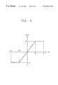
- FIG. 4 is a wave form diagram of an input/output signal from the voltage limiter of FIG. 3;
- FIGS. 5A and 5B are graphs illustrating an input/output voltage of a high output amplifier according to the present invention, of which:
- FIG. 5A is a graph illustrating a region in which an error is previously generated based on a signal generation probability distribution in accordance with an input voltage in a high output amplifier according to the present invention.
- FIG. 5B is a graph illustrating a probability distribution of a signal inputted into an input terminal of a high output amplifier according to the present invention.
- FIG. 3 is a block diagram illustrating a part of the transmission apparatus for a CDMA base station according to the present invention.
- the transmission apparatus for a CDMA base station includes a multiplexer 100 for multiplexing CDMA signals inputted through a plurality of channels CH.1 through CH.n, a voltage limiter 110 for limiting the voltage of the multiplexed signal, a BPF (Band Pass Filter) 120 for removing the signals out of a predetermined frequency band among the output signals from the voltage limiter 110 , an up-converter 130 for combining the filtered signal and a clock signal generated by the local oscillator 160 , a high power amplifier 130 for amplifying the up-converted signal to a predetermined transmission power level, and a duplexer 150 for transmitting the amplified signal through an antenna or transmitting the signal received through the antenna to the side of the receiving apparatus.
- a multiplexer 100 for multiplexing CDMA signals inputted through a plurality of channels CH.1 through CH.n
- a voltage limiter 110 for limiting the voltage of the multiplexed signal
- BPF Band Pass Filter
- the multiplexer 100 multiplexes the CDMA signals inputted from the channels CH.1 through CH.n and outputs one signal, and the voltage limiter 110 limits the voltage of the signal at a predetermined level.
- the voltage limiter 110 outputs the voltage above the K-volt as the K-volt level voltage so that a predetermined level(K) signal is not outputted.
- a predetermined band width signal among the signals inputted from the voltage limiter 110 is filtered by the BPF 120 , and the up-converter 130 combines the filtered signal and a clock signal generated by the local oscillator 160 , and the thusly combined signal is converted into a high frequency.
- the high power amplifier 140 amplifies the inputted signal to a predetermined power level required in accordance with a predetermined amplification ratio, and the thusly amplified signal is applied to the duplexer 150 and is transmitted through the antenna.
- the digital information transmitted trough the public line should be below 10 ⁇ 2 through 10 ⁇ 3 in the case that the bit error occurrence ratio of the digital signal is a voice signal, and the same should be below 10 ⁇ 6 in the case of the data signal.
- the above-described recommendation represents that the digital signal which is inputted through the digital transceiver generates an error below the above-described error standard to the side of the transmission.
- the peak power which is below the N 2 watt which is the peak power is recommended, so that the error ratio at the earlier stage is 1/10 through 1/100 compared to the error standard.
- the error which may not affect the digital signal error standard of the Qualcomm Co. is generated, an actual voice communication of the subscriber is not affected, and the high power amplifier which may be used in the case of the lower power may be used.
- FIGS. 5A and 5B in view of the signal occurrence probability with respect to the input voltage of the high power amplifier, as the voltage becomes lower, the occurrence probability of the signal becomes higher, and in the case of the higher voltage, the probability is geometrically decreased.
- the signal occurrence probability with respect to the voltage after the signals of each subscriber channel are multiplexed has a binomial distribution.
- the portion in which the voltage level is near +N or ⁇ N, the probability of the signal occurrence is in proportion to 2 ⁇ N .
- the probability that 30 channels occur as +1V or ⁇ 1V at the same time namely, the probability that the output voltage of the multiplexer 100 is +30V or ⁇ 30V, is 2 ⁇ 2 ⁇ 30 ⁇ 2 ⁇ 10 ⁇ 9 based on the binomial distribution. Therefore, when the voltage of +30V or ⁇ 30V is limited to +29V or ⁇ 29V by the voltage limiter 110 , the error occurrence ratio in the system is relatively lower compared to the error limitation standard of 10 ⁇ 2 through 10 ⁇ 3 or 10 ⁇ 6 .
- the noise component due to the output voltage limitation of the CDMA is improved by a processing gain of the receiver, so that the error ratio at the side of the receiving becomes smaller.
- the output level of the voltage limiter 110 at the level of ⁇ K in other words, the input voltage of the high power amplifier 140 may be limited.
- FIG. 5B illustrates that the signal occurrence probability with respect to the input voltage of the high power amplifier when the output voltage of the voltage limiter 110 is limited at ⁇ K volt.
- the +K volt signal is outputted, and in the case of below ⁇ K volts, the ⁇ K volt signal is outputted.
- the occurrence probability at the ⁇ K volts is increased more slightly compared to the case when the voltage is limited.
- the peak power of the high power amplifier may be expressed as follows:
- A Amplification ratio of high power amplifier
- the peak power of the high power amplifier 140 is A ⁇ K 2 watt based on Equation 5(K ⁇ N, and the peak power of the high power amplifier 140 is decreased at a ratio of (K/N) 2 .
- the CDMA base station transmission apparatus it is possible to maintain a bit error occurrence probability by which the performance of the base station system and the reliability of the same are determined and to decreased the peak power used for the high power amplifier. Therefore, it is possible to use a non-expensive high power amplifier, and the power consumption and the size of the transceiver of the CDMA base station system are decreased.
- the present invention is not limited to the base station transmission apparatus. Namely, the present invention may be used for a multiplex channel terminal and may be adapted for the multicode CDMA and OFDM (Orthogonal Frequency Division Multiplex) CDMA as well as the CDMA base station and terminals having large PAR.
- CDMA and OFDM Orthogonal Frequency Division Multiplex
Abstract
Description
Claims (7)
Applications Claiming Priority (2)
| Application Number | Priority Date | Filing Date | Title |
|---|---|---|---|
| KR98-50260 | 1998-11-23 | ||
| KR1019980050260A KR20000033412A (en) | 1998-11-23 | 1998-11-23 | Transmitting apparatus for cdma and method thereof |
Publications (1)
| Publication Number | Publication Date |
|---|---|
| US6473416B1 true US6473416B1 (en) | 2002-10-29 |
Family
ID=19559356
Family Applications (1)
| Application Number | Title | Priority Date | Filing Date |
|---|---|---|---|
| US09/223,747 Expired - Lifetime US6473416B1 (en) | 1998-11-23 | 1998-12-31 | Transmission apparatus for CDMA communication system |
Country Status (3)
| Country | Link |
|---|---|
| US (1) | US6473416B1 (en) |
| KR (1) | KR20000033412A (en) |
| CN (1) | CN1254997A (en) |
Cited By (4)
| Publication number | Priority date | Publication date | Assignee | Title |
|---|---|---|---|---|
| US20050094714A1 (en) * | 2003-10-31 | 2005-05-05 | Ian Robinson | Multi-carrier transceiver assembly |
| US7058037B1 (en) * | 1999-09-13 | 2006-06-06 | Utstarcom, Inc. | Radio frequency transmitting device of mobile radio communication base station system in code division multiple access system |
| US7427937B2 (en) | 2005-06-30 | 2008-09-23 | Infineon Technologies Ag | Multi-channel digital/analog converter arrangement |
| US20110267106A1 (en) * | 2005-05-16 | 2011-11-03 | Altera Corporation | Low-power routing multiplexers |
Citations (4)
| Publication number | Priority date | Publication date | Assignee | Title |
|---|---|---|---|---|
| US5132634A (en) * | 1991-03-25 | 1992-07-21 | Motorola, Inc. | Amplifier circuit with envelope smoothing |
| US5278994A (en) * | 1991-06-03 | 1994-01-11 | Motorola, Inc. | Power amplifier saturation detection and correction method and apparatus |
| US5426641A (en) * | 1994-01-28 | 1995-06-20 | Bell Communications Research, Inc. | Adaptive class AB amplifier for TDMA wireless communications systems |
| US5509011A (en) * | 1993-07-24 | 1996-04-16 | U.S. Philips Corporation | Transmission system for time-division multiplex signal transmission |
-
1998
- 1998-11-23 KR KR1019980050260A patent/KR20000033412A/en not_active IP Right Cessation
- 1998-12-31 US US09/223,747 patent/US6473416B1/en not_active Expired - Lifetime
-
1999
- 1999-01-25 CN CN99100254A patent/CN1254997A/en active Pending
Patent Citations (4)
| Publication number | Priority date | Publication date | Assignee | Title |
|---|---|---|---|---|
| US5132634A (en) * | 1991-03-25 | 1992-07-21 | Motorola, Inc. | Amplifier circuit with envelope smoothing |
| US5278994A (en) * | 1991-06-03 | 1994-01-11 | Motorola, Inc. | Power amplifier saturation detection and correction method and apparatus |
| US5509011A (en) * | 1993-07-24 | 1996-04-16 | U.S. Philips Corporation | Transmission system for time-division multiplex signal transmission |
| US5426641A (en) * | 1994-01-28 | 1995-06-20 | Bell Communications Research, Inc. | Adaptive class AB amplifier for TDMA wireless communications systems |
Cited By (6)
| Publication number | Priority date | Publication date | Assignee | Title |
|---|---|---|---|---|
| US7058037B1 (en) * | 1999-09-13 | 2006-06-06 | Utstarcom, Inc. | Radio frequency transmitting device of mobile radio communication base station system in code division multiple access system |
| US20050094714A1 (en) * | 2003-10-31 | 2005-05-05 | Ian Robinson | Multi-carrier transceiver assembly |
| US7869528B2 (en) * | 2003-10-31 | 2011-01-11 | Northrop Grumman Systems Corporation | Multi-carrier transceiver assembly |
| US20110267106A1 (en) * | 2005-05-16 | 2011-11-03 | Altera Corporation | Low-power routing multiplexers |
| US8405425B2 (en) * | 2005-05-16 | 2013-03-26 | Altera Corporation | Low-power routing multiplexers |
| US7427937B2 (en) | 2005-06-30 | 2008-09-23 | Infineon Technologies Ag | Multi-channel digital/analog converter arrangement |
Also Published As
| Publication number | Publication date |
|---|---|
| KR20000033412A (en) | 2000-06-15 |
| CN1254997A (en) | 2000-05-31 |
Similar Documents
| Publication | Publication Date | Title |
|---|---|---|
| US7145863B2 (en) | Mobile station, base station, communication system, and communication method | |
| EP1388937B1 (en) | Adaptive RF amplifier prelimiter | |
| JP2718398B2 (en) | CDMA base station transmitter | |
| EP1819081B1 (en) | Orthogonal complex spreading method for multichannel and apparatus thereof | |
| US6396868B1 (en) | Spread spectrum signal generating device and method in transmitter of mobile communications system | |
| KR100354337B1 (en) | Transmission and Receiving using Spreading Modulation for Spread Spectrum Communications and thereof Apparatus | |
| US5677929A (en) | Automobile on-board and/or portable telephone system | |
| US7773678B2 (en) | Method and apparatus for reducing the dynamic range of a radio signal | |
| JP2004500781A (en) | Dynamic bias for RF power amplifiers | |
| US8155170B2 (en) | Method and apparatus for achieving channel variability in spread spectrum communication systems | |
| US6473416B1 (en) | Transmission apparatus for CDMA communication system | |
| US6996080B1 (en) | Chip-synchronous CDMA multiplexer and method resulting in constant envelope signals | |
| JP3843562B2 (en) | Spread spectrum communication equipment | |
| US20040141546A1 (en) | Method and apparatus for ultra wideband communications system employing a spread spectrum technique transmitting a baseband signal over a wide frequency band | |
| US7609749B1 (en) | Method and apparatus for generating non-recursive variable rate orthogonal spreading codes | |
| US6580702B1 (en) | Data transmission apparatus for CDMA communication system and method thereof | |
| USRE39954E1 (en) | Automobile on-board and/or portable telephone system | |
| Zhang et al. | Performance comparison of two spread-spectrum-based wireless video transmission schemes | |
| JP2944612B1 (en) | Code division multiplex communication equipment | |
| JPH1093531A (en) | Code division multiplex communication equipment | |
| Chang et al. | A Constant Amplitude Multiplexing for Multi-Code DS/CDMA Systems |
Legal Events
| Date | Code | Title | Description |
|---|---|---|---|
| AS | Assignment |
Owner name: LG INFORMATION & COMMUNICATIONS, LTD., KOREA, REPU Free format text: ASSIGNMENT OF ASSIGNORS INTEREST;ASSIGNOR:LEE, KYUNG KUK;REEL/FRAME:009696/0029 Effective date: 19981221 |
|
| STCF | Information on status: patent grant |
Free format text: PATENTED CASE |
|
| FEPP | Fee payment procedure |
Free format text: PAYOR NUMBER ASSIGNED (ORIGINAL EVENT CODE: ASPN); ENTITY STATUS OF PATENT OWNER: LARGE ENTITY |
|
| AS | Assignment |
Owner name: LG ELECTRONICS INC., KOREA, REPUBLIC OF Free format text: MERGER;ASSIGNOR:LG INFORMATION & COMMUNICATIONS, LTD.;REEL/FRAME:017153/0155 Effective date: 20000904 |
|
| FPAY | Fee payment |
Year of fee payment: 4 |
|
| AS | Assignment |
Owner name: LG NORTEL CO., LTD., KOREA, REPUBLIC OF Free format text: ASSIGNMENT OF ASSIGNORS INTEREST;ASSIGNOR:LG ELECTRONICS INC.;REEL/FRAME:018296/0720 Effective date: 20060710 |
|
| FPAY | Fee payment |
Year of fee payment: 8 |
|
| AS | Assignment |
Owner name: LG-ERICSSON CO., LTD., KOREA, REPUBLIC OF Free format text: CHANGE OF NAME;ASSIGNOR:LG-NORTEL CO., LTD.;REEL/FRAME:025948/0842 Effective date: 20100630 |
|
| FEPP | Fee payment procedure |
Free format text: PAYER NUMBER DE-ASSIGNED (ORIGINAL EVENT CODE: RMPN); ENTITY STATUS OF PATENT OWNER: LARGE ENTITY Free format text: PAYOR NUMBER ASSIGNED (ORIGINAL EVENT CODE: ASPN); ENTITY STATUS OF PATENT OWNER: LARGE ENTITY |
|
| FPAY | Fee payment |
Year of fee payment: 12 |