US6476443B1 - MOSgated device with trench structure and remote contact and process for its manufacture - Google Patents
MOSgated device with trench structure and remote contact and process for its manufacture Download PDFInfo
- Publication number
- US6476443B1 US6476443B1 US09/416,796 US41679699A US6476443B1 US 6476443 B1 US6476443 B1 US 6476443B1 US 41679699 A US41679699 A US 41679699A US 6476443 B1 US6476443 B1 US 6476443B1
- Authority
- US
- United States
- Prior art keywords
- trenches
- microns
- depth
- substrate
- gate
- Prior art date
- Legal status (The legal status is an assumption and is not a legal conclusion. Google has not performed a legal analysis and makes no representation as to the accuracy of the status listed.)
- Expired - Lifetime
Links
- 238000000034 method Methods 0.000 title description 14
- 238000004519 manufacturing process Methods 0.000 title description 11
- 229910021420 polycrystalline silicon Inorganic materials 0.000 claims abstract description 40
- 229920005591 polysilicon Polymers 0.000 claims abstract description 40
- 239000000758 substrate Substances 0.000 claims description 21
- 238000009413 insulation Methods 0.000 claims description 15
- 238000009792 diffusion process Methods 0.000 claims description 10
- 239000004065 semiconductor Substances 0.000 claims description 3
- 239000000463 material Substances 0.000 claims description 2
- 239000011248 coating agent Substances 0.000 claims 1
- 238000000576 coating method Methods 0.000 claims 1
- XUIMIQQOPSSXEZ-UHFFFAOYSA-N Silicon Chemical compound [Si] XUIMIQQOPSSXEZ-UHFFFAOYSA-N 0.000 abstract description 8
- 229910052710 silicon Inorganic materials 0.000 abstract description 8
- 239000010703 silicon Substances 0.000 abstract description 8
- 108091006146 Channels Proteins 0.000 description 35
- 230000015572 biosynthetic process Effects 0.000 description 6
- 239000007943 implant Substances 0.000 description 6
- 229910052782 aluminium Inorganic materials 0.000 description 5
- XAGFODPZIPBFFR-UHFFFAOYSA-N aluminium Chemical compound [Al] XAGFODPZIPBFFR-UHFFFAOYSA-N 0.000 description 5
- 230000015556 catabolic process Effects 0.000 description 5
- VYPSYNLAJGMNEJ-UHFFFAOYSA-N Silicium dioxide Chemical compound O=[Si]=O VYPSYNLAJGMNEJ-UHFFFAOYSA-N 0.000 description 4
- 238000011065 in-situ storage Methods 0.000 description 4
- ZOXJGFHDIHLPTG-UHFFFAOYSA-N Boron Chemical compound [B] ZOXJGFHDIHLPTG-UHFFFAOYSA-N 0.000 description 3
- 108010075750 P-Type Calcium Channels Proteins 0.000 description 3
- 230000002457 bidirectional effect Effects 0.000 description 3
- 229910052796 boron Inorganic materials 0.000 description 3
- 238000010438 heat treatment Methods 0.000 description 3
- 229910052751 metal Inorganic materials 0.000 description 3
- 239000002184 metal Substances 0.000 description 3
- IJGRMHOSHXDMSA-UHFFFAOYSA-N Atomic nitrogen Chemical compound N#N IJGRMHOSHXDMSA-UHFFFAOYSA-N 0.000 description 2
- XYFCBTPGUUZFHI-UHFFFAOYSA-N Phosphine Chemical compound P XYFCBTPGUUZFHI-UHFFFAOYSA-N 0.000 description 2
- BOTDANWDWHJENH-UHFFFAOYSA-N Tetraethyl orthosilicate Chemical compound CCO[Si](OCC)(OCC)OCC BOTDANWDWHJENH-UHFFFAOYSA-N 0.000 description 2
- BHEPBYXIRTUNPN-UHFFFAOYSA-N hydridophosphorus(.) (triplet) Chemical compound [PH] BHEPBYXIRTUNPN-UHFFFAOYSA-N 0.000 description 2
- 230000004048 modification Effects 0.000 description 2
- 238000012986 modification Methods 0.000 description 2
- 230000003647 oxidation Effects 0.000 description 2
- 238000007254 oxidation reaction Methods 0.000 description 2
- 235000012239 silicon dioxide Nutrition 0.000 description 2
- 239000000377 silicon dioxide Substances 0.000 description 2
- BLRPTPMANUNPDV-UHFFFAOYSA-N Silane Chemical compound [SiH4] BLRPTPMANUNPDV-UHFFFAOYSA-N 0.000 description 1
- 229910052785 arsenic Inorganic materials 0.000 description 1
- RQNWIZPPADIBDY-UHFFFAOYSA-N arsenic atom Chemical compound [As] RQNWIZPPADIBDY-UHFFFAOYSA-N 0.000 description 1
- 230000001413 cellular effect Effects 0.000 description 1
- 238000004140 cleaning Methods 0.000 description 1
- 238000005520 cutting process Methods 0.000 description 1
- 230000008021 deposition Effects 0.000 description 1
- 239000002019 doping agent Substances 0.000 description 1
- 239000012774 insulation material Substances 0.000 description 1
- 239000012212 insulator Substances 0.000 description 1
- 229910052757 nitrogen Inorganic materials 0.000 description 1
- 238000005457 optimization Methods 0.000 description 1
- 230000000149 penetrating effect Effects 0.000 description 1
- 229910000073 phosphorus hydride Inorganic materials 0.000 description 1
- 238000000206 photolithography Methods 0.000 description 1
- 229920002120 photoresistant polymer Polymers 0.000 description 1
- 229910000077 silane Inorganic materials 0.000 description 1
- XUIMIQQOPSSXEZ-RNFDNDRNSA-N silicon-32 atom Chemical compound [32Si] XUIMIQQOPSSXEZ-RNFDNDRNSA-N 0.000 description 1
- 125000006850 spacer group Chemical group 0.000 description 1
Images


Classifications
-
- H—ELECTRICITY
- H01—ELECTRIC ELEMENTS
- H01L—SEMICONDUCTOR DEVICES NOT COVERED BY CLASS H10
- H01L29/00—Semiconductor devices adapted for rectifying, amplifying, oscillating or switching, or capacitors or resistors with at least one potential-jump barrier or surface barrier, e.g. PN junction depletion layer or carrier concentration layer; Details of semiconductor bodies or of electrodes thereof ; Multistep manufacturing processes therefor
- H01L29/02—Semiconductor bodies ; Multistep manufacturing processes therefor
- H01L29/06—Semiconductor bodies ; Multistep manufacturing processes therefor characterised by their shape; characterised by the shapes, relative sizes, or dispositions of the semiconductor regions ; characterised by the concentration or distribution of impurities within semiconductor regions
- H01L29/0684—Semiconductor bodies ; Multistep manufacturing processes therefor characterised by their shape; characterised by the shapes, relative sizes, or dispositions of the semiconductor regions ; characterised by the concentration or distribution of impurities within semiconductor regions characterised by the shape, relative sizes or dispositions of the semiconductor regions or junctions between the regions
- H01L29/0692—Surface layout
- H01L29/0696—Surface layout of cellular field-effect devices, e.g. multicellular DMOS transistors or IGBTs
-
- H—ELECTRICITY
- H01—ELECTRIC ELEMENTS
- H01L—SEMICONDUCTOR DEVICES NOT COVERED BY CLASS H10
- H01L29/00—Semiconductor devices adapted for rectifying, amplifying, oscillating or switching, or capacitors or resistors with at least one potential-jump barrier or surface barrier, e.g. PN junction depletion layer or carrier concentration layer; Details of semiconductor bodies or of electrodes thereof ; Multistep manufacturing processes therefor
- H01L29/40—Electrodes ; Multistep manufacturing processes therefor
- H01L29/41—Electrodes ; Multistep manufacturing processes therefor characterised by their shape, relative sizes or dispositions
- H01L29/417—Electrodes ; Multistep manufacturing processes therefor characterised by their shape, relative sizes or dispositions carrying the current to be rectified, amplified or switched
- H01L29/41725—Source or drain electrodes for field effect devices
- H01L29/41741—Source or drain electrodes for field effect devices for vertical or pseudo-vertical devices
-
- H—ELECTRICITY
- H01—ELECTRIC ELEMENTS
- H01L—SEMICONDUCTOR DEVICES NOT COVERED BY CLASS H10
- H01L29/00—Semiconductor devices adapted for rectifying, amplifying, oscillating or switching, or capacitors or resistors with at least one potential-jump barrier or surface barrier, e.g. PN junction depletion layer or carrier concentration layer; Details of semiconductor bodies or of electrodes thereof ; Multistep manufacturing processes therefor
- H01L29/66—Types of semiconductor device ; Multistep manufacturing processes therefor
- H01L29/68—Types of semiconductor device ; Multistep manufacturing processes therefor controllable by only the electric current supplied, or only the electric potential applied, to an electrode which does not carry the current to be rectified, amplified or switched
- H01L29/76—Unipolar devices, e.g. field effect transistors
- H01L29/772—Field effect transistors
- H01L29/78—Field effect transistors with field effect produced by an insulated gate
- H01L29/7801—DMOS transistors, i.e. MISFETs with a channel accommodating body or base region adjoining a drain drift region
- H01L29/7802—Vertical DMOS transistors, i.e. VDMOS transistors
- H01L29/7813—Vertical DMOS transistors, i.e. VDMOS transistors with trench gate electrode, e.g. UMOS transistors
-
- H—ELECTRICITY
- H01—ELECTRIC ELEMENTS
- H01L—SEMICONDUCTOR DEVICES NOT COVERED BY CLASS H10
- H01L29/00—Semiconductor devices adapted for rectifying, amplifying, oscillating or switching, or capacitors or resistors with at least one potential-jump barrier or surface barrier, e.g. PN junction depletion layer or carrier concentration layer; Details of semiconductor bodies or of electrodes thereof ; Multistep manufacturing processes therefor
- H01L29/40—Electrodes ; Multistep manufacturing processes therefor
- H01L29/41—Electrodes ; Multistep manufacturing processes therefor characterised by their shape, relative sizes or dispositions
- H01L29/417—Electrodes ; Multistep manufacturing processes therefor characterised by their shape, relative sizes or dispositions carrying the current to be rectified, amplified or switched
- H01L29/41725—Source or drain electrodes for field effect devices
- H01L29/41766—Source or drain electrodes for field effect devices with at least part of the source or drain electrode having contact below the semiconductor surface, e.g. the source or drain electrode formed at least partially in a groove or with inclusions of conductor inside the semiconductor
-
- H—ELECTRICITY
- H01—ELECTRIC ELEMENTS
- H01L—SEMICONDUCTOR DEVICES NOT COVERED BY CLASS H10
- H01L29/00—Semiconductor devices adapted for rectifying, amplifying, oscillating or switching, or capacitors or resistors with at least one potential-jump barrier or surface barrier, e.g. PN junction depletion layer or carrier concentration layer; Details of semiconductor bodies or of electrodes thereof ; Multistep manufacturing processes therefor
- H01L29/40—Electrodes ; Multistep manufacturing processes therefor
- H01L29/41—Electrodes ; Multistep manufacturing processes therefor characterised by their shape, relative sizes or dispositions
- H01L29/423—Electrodes ; Multistep manufacturing processes therefor characterised by their shape, relative sizes or dispositions not carrying the current to be rectified, amplified or switched
- H01L29/42312—Gate electrodes for field effect devices
- H01L29/42316—Gate electrodes for field effect devices for field-effect transistors
- H01L29/4232—Gate electrodes for field effect devices for field-effect transistors with insulated gate
- H01L29/42356—Disposition, e.g. buried gate electrode
- H01L29/4236—Disposition, e.g. buried gate electrode within a trench, e.g. trench gate electrode, groove gate electrode
-
- H—ELECTRICITY
- H01—ELECTRIC ELEMENTS
- H01L—SEMICONDUCTOR DEVICES NOT COVERED BY CLASS H10
- H01L29/00—Semiconductor devices adapted for rectifying, amplifying, oscillating or switching, or capacitors or resistors with at least one potential-jump barrier or surface barrier, e.g. PN junction depletion layer or carrier concentration layer; Details of semiconductor bodies or of electrodes thereof ; Multistep manufacturing processes therefor
- H01L29/66—Types of semiconductor device ; Multistep manufacturing processes therefor
- H01L29/68—Types of semiconductor device ; Multistep manufacturing processes therefor controllable by only the electric current supplied, or only the electric potential applied, to an electrode which does not carry the current to be rectified, amplified or switched
- H01L29/76—Unipolar devices, e.g. field effect transistors
- H01L29/772—Field effect transistors
- H01L29/78—Field effect transistors with field effect produced by an insulated gate
- H01L29/7801—DMOS transistors, i.e. MISFETs with a channel accommodating body or base region adjoining a drain drift region
- H01L29/7802—Vertical DMOS transistors, i.e. VDMOS transistors
- H01L29/7811—Vertical DMOS transistors, i.e. VDMOS transistors with an edge termination structure
Definitions
- This invention relates to MOSgated semiconductor devices and more specifically, relates to such devices with a trench geometry and a remote contact structure.
- MOSgated devices are well known and may have a planar channel geometry or a trench channel geometry.
- spaced channel regions are diffused into the surface of a chip and MOSgates cover the invertible channel regions which are coplanar with one another.
- MOSgates cover the invertible channel regions which are coplanar with one another.
- invertible channel regions are formed along the vertical walls of U-shaped trenches etched into the silicon surface.
- a source contact is connected to the channel region and source region for each separate trench unit.
- Trench devices are preferably used for lower breakdown voltage ratings, for example, less than about 100 volts.
- planar geometry devices and trench geometry devices may be formed with channel regions of a spaced polygonal or spaced stripe arrangement.
- Trench geometry devices have an inherently lower capacitance between gate and drain, and thus a lower charge Q GD than planar devices. Since an important figure of merit of a MOSFET is the product of Q GD and the on-resistance R DSON , trench devices are frequently desired for low voltage applications requiring a minimum switching loss such as the MOSFETs used in low voltage power supplies for supplying power from a battery to a portable electronic device such as a lap top computer.
- Trench device geometries have not permitted the best trench density for minimizing the R DSON . Therefore, while the trench device has a low Q GD , complex manufacturing processes are needed to produce a low R DSON as well.
- i t is desirable to provide a trench geometry Mosgated device such as a MOSFET, which has a minimized Q GD and R DSON but is capable of inexpensive and reliable production techniques.
- a novel trench structure and manufacturing process in which both a very low Q GD and R DSON , is provided through the use of a common polysilicon layer for a plurality of adjacent trenches, with contacts to the source and channel region being remote from the trench areas.
- the trenches can be more closely spaced, to increase total channel width per unit area.
- the Q GD is also reduced by the use of a unique trench mesa height and control of the trench bottom relative to the P/N junction which defines the bottom of the invertible channel along the walls of the trench. More specifically, a trench depth (or mesa height) of about 1.8 microns is used, with the trench bottom penetrating the P/N junction by about 0.2 to 0.25 microns.
- the novel trench structure is also preferred to have a length less than about 20 microns and a width of about 0.6 microns.
- the trenches are arranged in parallel, coextensive groups with a spacing greater than about 0.6 microns.
- the trenches are filled with a common polysilicon layer which acts as the device gate.
- Each parallel set of trenches are spaced from an adjacent set by a strip of untrenched area running perpendicular to the elongated trenches.
- the source/base contacts are formed in this strip, remotely from the trench structures, but connected to the channel region and source region for each trench.
- a bidirectional conductive device By making contact only to the source region, a bidirectional conductive device can be formed.
- the novel device lends itself to a simplified manufacturing process having a reduced number of masks and critical mask alignments and has a minimized figure of merit.
- FIG. 1 is a cross-section of one cell of a prior art planar geometry MOSFET.
- FIG. 2 is a cross-section of one cell of a second prior art planar geometry MOSFET.
- FIG. 3 is a cross-section of one cell element of a prior art trench geometry device.
- FIG. 4 is a top view of a die which may incorporate the present invention.
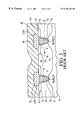
- FIG. 5 is a cross-section of the active area of the chip of FIG. 4 at region “A” in FIG. 4 and shows the trench structure and common polysilicon gate of the present invention and is a cross-section of FIG. 6 taken across section line 5 — 5 in FIG. 6 .
- FIG. 6 is a top schematic view of region “A” of FIG. 4 to show two rows of trenches and their remote source contacts with the upper polysilicon layer removed.
- FIG. 7 is a cross-section of FIG. 6 taken across section line 7 — 7 in FIG. 6 to show the source contact structure between rows of trenches in FIG. 6 .
- FIG. 8 is a cross-section of the die area “B” in FIG. 4 and shows the termination structure which surrounds the die of FIG. 4 .
- FIG. 9 is a top schematic view of the termination topology at region 5 of FIGS. 4 and 8.
- FIG. 10 is a cross-section of a small portion of a die, showing the first steps in the manufacture of a device containing the invention.
- FIG. 11 is a cross-section of the die portion of FIG. 10 following diffusion steps for forming the regions which will become the source and channel regions.
- FIG. 12 is a cross-section of the structure of FIG. 11 after the formation of typical trenches.
- FIG. 13 is a cross-section of the structure of FIG. 12 after the formation of gate oxide in the trenches and the formation of a layer of in-situ-doped polysilicon.
- FIG. 14 is a cross-section of a portion of space between rows of trenches preparatory to the formation of the source/channel contact.
- FIG. 15 is the cross-section of FIG. 14 after the formation of contact regions for the source/channel contact, and prior to the steps which complete the active regions as shown in FIG. 5 .
- FIG. 1 shows, in cross-section, a single power MOSFET cell 30 of a power MOSFET made in accordance with the disclosure of U.S. Pat. No. 5,731,604, the disclosure of which is incorporated herein by reference.
- Cell 30 is one of a large number of spaced polygonal planar cells which each include a P-type channel diffusion region 31 (sometimes referred to as a base region) in a low resistivity, epitaxially formed substrate 32 .
- Channel region 31 receives a P + diffusion 33 and an N + source diffusion 34 .
- the area between the outer periphery of source region 34 at its upper surface, and extending to the periphery of P region 31 defines a planar invertible channel region 35 .
- Channel region 35 is covered by a layer of silicon dioxide 36 , which defines a gate insulation layer and the gate insulation layer is covered by a conductive polysilicon layer 37 which is a conductive gate electrode sometimes referred to as gate poly.
- the polysilicon layer 37 is insulated from a continuous aluminum source electrode 38 by an insulation layer 39 which usually is a deposited low temperature oxide or an LTO layer. Other insulation materials can be used.
- a drain electrode, not shown, is fixed to the bottom of a 375 micron thick N ++ body (not shown) which carries the N-epitaxial layer 32 . Note that source electrode 38 contacts both N + source region 34 and P + region 33 in the etched opening 40 in silicon 32 .
- the source diffusion 34 has a depth of about 0.4 microns and the P base 31 has a depth of about 1.9 microns.
- the capacitance between the gate 37 and the drain 32 is relatively high in a planar design such as that of FIG. 1 so that the charge QGD is high, for example, greater than about 12.3.
- the figure of merit or R DSON X Q GD is about 115 (m ⁇ nc).
- FIG. 2 shows another cell configuration which is similar to that of FIG. 1 and similar numerals designate similar structures.
- the structure shown in FIG. 2 is that of copending application Ser. No. 08/956,062 filed Oct. 22, 1997 (IR-1232), the disclosure of which is incorporated by reference into this application.
- the device of FIG. 2 differs basically from that of FIG. 1 only in using a side insulation spacer insulation 50 for LTO 39 , rather than photo lithography step to define the contact opening 40 .
- the figure of merit for such devices exceeds about 128 (m ⁇ nc).
- the figure of merit can be reduced in a stripe trench design by careful optimization of the trench depth and P base depth.
- FIG. 3 schematically shows the cross-section of a known trench device which has an N- epitaxial substrate 51 which has a plurality of parallel trenches, two of which are shown as trenches 52 and 53 , formed in a P type channel 54 .
- N + source regions 55 - 56 extend the length of the trenches, as shown for trench 52 .
- Trenches 52 and 53 are then lined with gate oxides 57 and 58 respectively and are filled with polysilicon strips 59 and 60 respectively.
- Strips 59 and 60 are necessarily interrupted at the top surface of silicon 51 , but are connected together at some other region of the die, not shown, and are connected to a common gate electrode 61 .
- the tops of polysilicon strips 59 and 60 and a portion of source regions 55 and 56 are insulated from an aluminum source electrode 62 by LTO strips 63 and 64 .
- the structure of FIG. 3 is a trench structure in which invertible channels are formed in the P material lining the vertical walls of trenches 52 and 53 and which extend from sources 55 - 56 to N-region 51 .
- the structure has a low RDSON and so was thought to be the preferred structure for power MOSgated devices intended for use at low voltages, for example, voltages lower than about 40 volts.
- the present invention provides a novel design for trench type devices which provides simplified manufacturing techniques and an improved trade off of such variable as Q GD and R DSON to provide a low voltage device with a reduced figure of merit and reduced cost, as compared to known devices.
- FIGS. 4 to 9 The structure of the novel device of the invention is shown in FIGS. 4 to 9 , and one process of manufacture for the structure is shown in FIGS. 10 to 15 .
- FIG. 4 there is shown the top view of a typical die 70 containing the structure of the present invention.
- Die 70 may have a width of 102 mils and a length of 157 mils (the largest size that can fit into an SO8 style package), although the die may have any desired dimensions.
- the die has a top source electrode 71 , a gate pad 72 to which a polysilicon gate is connected, as will be later described, and has a bottom drain electrode 73 , shown in FIG. 5 .
- FIGS. 5 and 7 A small portion of the active trench area of the die of FIG. 4, shown within circle “A” is shown in detail in FIGS. 5 and 7.
- a small portion of the termination of the die of FIG. 4, shown within circle “B” is shown in more detail in FIGS. 8 and 9.
- the device to be described has an improved active area utilization of almost 84%, using a reduced area termination, a small gate pad 72 (6 mil ⁇ 6 mil) and a small street width (where die are separated within a wafer) of about 3.1 mils.
- the gate busses (not shown) extend parallel to the direction of the trenches to permit unrestricted current flow and reduced gate resistance (of about 2.5 ohms) in the die of FIG. 4 .
- the active area “A” as shown in FIGS. 5, 6 and 7 is shown for a vertical conduction type device having an N + body 80 , to which drain contact 73 is connected and which receives and N ⁇ epitaxially deposited, junction receiving layer 81 .
- a P type channel diffusion 82 is formed into the upper planar surface of N ⁇ substrate layer 81 to a first depth, for example, 1.5 to 1.6 microns.
- a shallow N + source region 83 is formed into the upper surface of region 81 to a second depth, for example 0.3 to 0.4 ⁇ .
- a plurality of rows of parallel, coextensive trenches 85 are then etched into the surface of substrate 81 to a third depth which is greater than the depth of P diffusion 82 , preferably by 0.2 to 0.25 microns.
- parallel trenches 85 have a depth of about 1.8 microns, cutting through source layer 83 and channel layer 82 as shown.
- FIG. 6 shows the silicon surface as containing first and second rows 86 and 87 of trenches 85 , separated by a central untrenched area 88 which will be later described to be the area to receive remote source/channel contacts for the device, permitting a very close high density spacing of the trenches.
- trenches 85 have a width of about 0.6 microns and a length of about 5-8 microns.
- the trench spacing should be equal to or greater than about 0.6 microns.
- the space 88 between rows 86 and 87 should be as small as possible, to conserve active trench area.
- each of trenches 85 are lined with a grown silicon dioxide gate insulation layer 90 which may have a thickness of 300 to 500 ⁇ .
- the interior of each of the gate oxide lined trenches is then filled with a conductive polysilicon layer 95 which acts as the device gate.
- the polysilicon layer 95 is insulated from, but extends continuously across the upper surface of the substrate between each of the trenches 85 .
- FIG. 3 the conventional polysilicon gate structure of prior art devices as shown in FIG. 3, in which the polysilicon strips of each “cell” is separated from adjacent ones by the source contact structure.
- the adjacent cells of FIG. 5 may be closer to one another, and more densely packed, (producing a greater channel width per unit area) with the source contact made to a location which is laterally remote from the trench.
- the upper surface of the polysilicon layer is then covered with a TEOS insulator layer 96 or other suitable insulation layer to insulate the polysilicon gate electrode layer 95 from the source electrode 71 .
- the contact structure disclosed in U.S. Pat. No. 5,731,604 may be used, as schematically shown in FIGS. 6 and 7.
- a plurality of openings are made in the region 88 , shown as polygonal (rectangular) etched frames 101 and 102 which encircle rectangular contact windows 101 a , 102 a that permit contact of aluminum source electrode 71 to the source region 83 and the channel region 82 at spaced locations along row 88 in FIG. 6.
- a shallow silicon trench 101 b , 102 b is etched in the contact window to expose the P-base 82 for contact.
- These contact regions can have any desired spacing from one another, and are preferably shorter in the direction of elongation of the trenches to reduce the width area needed for this source contact.
- the contacts have a pitch perpendicular to the direction of elongation of the trenches of about 4.8 microns.
- FIGS. 8 and 9 schematically illustrate a termination structure which can be used for the die of FIG. 4 .
- a small area termination may be used, comprising a polysilicon field plate 110 (defined by an extension of polysilicon layer 95 ), a gap 111 in the polysilicon layer 95 and an EQR ring 112 , also defined by an extension of the polysilicon layer 95 .
- FIGS. 4 to 9 There is next described a novel process for the manufacture of the trench MOSgated device of FIGS. 4 to 9 .
- the device to be made is for a power MOSFET rated at a voltage of 30 volts and having a die size of 102 by 157 mils.
- the numerals which described elements of the die in FIGS. 4 to 9 are used in FIGS. 10 to 15 to identify similar parts.
- the first step in the process is to select a silicon wafer having a main N + body 80 which is 375 microns thick and has a resistivity of 0.003 ⁇ cm.
- the upper surface of the wafer has the N ⁇ epitaxial layer 81 grown thereon.
- Layer 81 is phosphorous doped and is 5 microns thick and has a resistivity of 0.2 ⁇ cm for a 30 volt device.
- a field oxide layer 115 is first grown atop layer 81 to a thickness of 7500 ⁇ in an oxidation step in steam at 1050° C.
- a mask step is then carried out to mask the field oxide in the termination region and to open the active area of the device by a suitable etch and strip step.
- a boron implant is carried out, to form P region 82 .
- the boron implant dose is 7E13 at 120 kV.
- the boron is then driven to a depth of 1.5 to 1.6 micron by a drive at 1175° C. for 30 minutes.
- the source region 83 is next formed, using an arsenic implant at a dose of 1E16 at 50 kV. This is followed by heating at 900° C. for 30 minutes in nitrogen to preanneal the implant, and then by heating at 900° C. for 10 minutes in steam, to grow an oxide layer 120 to a thickness of about 2000 ⁇ .
- a second mask step is then carried out to define trenches in the active area.
- a dry plasma etch is then carried out to etch the spaced trenches as shown in FIG. 12 .
- the trench depth is preferably 1.7 to 1.8 microns, which has been found to lead to the most advantageous trade-off between Q GD and R DSON in the completed device.
- the trench etch should be almost 0.2 to 0.25 microns deeper than the P channel region 82 .
- Making the trench deeper improves R DSON but reduces breakdown voltage.
- Making the trench shallower reduces Q DG but creates a higher R DSON .
- a trench depth of about 1.8 microns and about 0.2 to 0.25 microns deeper than the P channel has been found to produce the most advantageous trade-offs between Q DG , R DSON and breakdown voltage.
- the trench length must be carefully chosen to prevent easy failure due to a low avalanche energy (due to a long current path and a high Rb 1 in N + source regions 83 ).
- 8 microns is preferred when using a trench to trench spacing of 0.6 microns for trenches with openings of 0.6 microns.
- the trench length can be increased to about 14 microns without being unduly “weak” to avalanche energy.
- the photoresist is stripped and the wafer is deglassed and cleaned.
- a sacrificial oxide is next grown by heating the wafer to 950° C. in steam and then deglassing and removing the grown oxide and cleaning the wafer.
- a gate oxide preferably a TCA oxidation step is then carried out at 950° C. to grow the gate oxide layer 90 to a thickness of 300 to 500 ⁇ , as shown in FIG. 13 . Note that oxide layer 90 overlies the oxide 120 which spans across the silicon surface between trenches and thickens the oxide layer on the spanning surfaces.
- the conductive polysilicon layer 95 is grown over the active surface of the device (and in the termination regions).
- in-situ polysilicon doping should be used in which the polysilicon is deposited with in-situ dopants, for example, using silane plus phosphine. It has been found that the use of in-situ doping leads to a reduction in threshold voltage of about 0.5 volts compared to an undoped film.
- a POCl 3 -doped poly film can be used, if the phosphorous is driven to the bottom of the trench.
- a preferred process employs the initial formation of an undoped polysilicon layer about 1000 ⁇ thick, followed by the deposition of 6500 ⁇ thick in-situ doped polysilicon. This process forms a polysilicon layer 95 having a thickness of 7500 ⁇ which completely fills the interiors of the oxide coated trenches 85 , and overlies the oxide over the planar silicon surface bridges between trenches.
- the next step in the process employs a third polysilicon mask, used to open the polysilicon layer 95 at locations in areas such as area 88 in FIG. 6 to receive the source/channel contact, and in the termination region to form the gap 111 (FIGS. 8 and 9) in the termination area to define and separate the field plate 110 and EQR ring 112 .
- a third polysilicon mask used to open the polysilicon layer 95 at locations in areas such as area 88 in FIG. 6 to receive the source/channel contact, and in the termination region to form the gap 111 (FIGS. 8 and 9) in the termination area to define and separate the field plate 110 and EQR ring 112 .
- the polysilicon layer 95 in patterned and then etched away to open windows 130 , 131 and 132 in the polysilicon layer 95 and the underlying oxide layer 120 , 90 .
- a plasma etch is preferably used.
- the TEOS layer 96 is formed to a thickness of 7500 ⁇ .
- a fourth mask which is the contact mask, is applied to define the source/channel openings in the rows such as row 88 and, using the process sequence of copending application Ser. No. 08/956,062 (IR-1232), the trenches 101 , 102 and 103 are etched through the N + layer 83 and into the top of the P channel layer 82 .
- the edge of oxide layer 120 , 90 is preferably etched back slightly.
- P + base implant 140 (not shown in FIG. 7) which is annealed at 900° C. for about 30 minutes.
- P + base implant 140 reduces the device R b (base resistance).
- the wafer is next deglassed and cleaned and the aluminum source metal 71 is applied to the device surface, making contact to the source region 83 and P channel.
- a fifth mask (the metal mask) is next applied to define the gate and 72 (FIG. 4) and gate busses (not shown) which run parallel to the direction of elongation of the trenches 85 .
- N + region 80 (FIG. 5) is then ground to reduce its thickness to about 200 microns.
- the surface is first ground with a rough grind, followed by grinding with a smoother grind, followed by an etch to cause stress relief of the ground surface.
- a suitable back side metal 73 is then applied to the back of the device.
- the wafer is then tested and the die are separated in the customary manner.
- the die may then be housed, for example, in SO-8 type housings.
- the above described process and device is for the manufacture of a power MOSFET which has a reduced figure of merit. Numerous variations are possible to adjust the device process and to make other kinds of MoSgated device, for example, IGBTs.
- the process can be altered to make a bidirectional type of MOSFET.
- the process in making contact to the rows 88 , if the aluminum source 71 in FIG. 15 contacts only the source 83 and not the channel region, then device can be used for bidirectional operation in applications with low dV/dt duty.
Abstract
Description
Claims (43)
Priority Applications (2)
| Application Number | Priority Date | Filing Date | Title |
|---|---|---|---|
| US09/416,796 US6476443B1 (en) | 1998-10-14 | 1999-10-13 | MOSgated device with trench structure and remote contact and process for its manufacture |
| US10/242,015 US6610574B2 (en) | 1998-10-14 | 2002-09-11 | Process for forming MOSgated device with trench structure and remote contact |
Applications Claiming Priority (2)
| Application Number | Priority Date | Filing Date | Title |
|---|---|---|---|
| US10414898P | 1998-10-14 | 1998-10-14 | |
| US09/416,796 US6476443B1 (en) | 1998-10-14 | 1999-10-13 | MOSgated device with trench structure and remote contact and process for its manufacture |
Related Child Applications (1)
| Application Number | Title | Priority Date | Filing Date |
|---|---|---|---|
| US10/242,015 Division US6610574B2 (en) | 1998-10-14 | 2002-09-11 | Process for forming MOSgated device with trench structure and remote contact |
Publications (1)
| Publication Number | Publication Date |
|---|---|
| US6476443B1 true US6476443B1 (en) | 2002-11-05 |
Family
ID=22298897
Family Applications (3)
| Application Number | Title | Priority Date | Filing Date |
|---|---|---|---|
| US09/292,186 Expired - Fee Related US7462910B1 (en) | 1998-10-14 | 1999-04-15 | P-channel trench MOSFET structure |
| US09/416,796 Expired - Lifetime US6476443B1 (en) | 1998-10-14 | 1999-10-13 | MOSgated device with trench structure and remote contact and process for its manufacture |
| US10/242,015 Expired - Lifetime US6610574B2 (en) | 1998-10-14 | 2002-09-11 | Process for forming MOSgated device with trench structure and remote contact |
Family Applications Before (1)
| Application Number | Title | Priority Date | Filing Date |
|---|---|---|---|
| US09/292,186 Expired - Fee Related US7462910B1 (en) | 1998-10-14 | 1999-04-15 | P-channel trench MOSFET structure |
Family Applications After (1)
| Application Number | Title | Priority Date | Filing Date |
|---|---|---|---|
| US10/242,015 Expired - Lifetime US6610574B2 (en) | 1998-10-14 | 2002-09-11 | Process for forming MOSgated device with trench structure and remote contact |
Country Status (4)
| Country | Link |
|---|---|
| US (3) | US7462910B1 (en) |
| JP (1) | JP3365984B2 (en) |
| DE (1) | DE19949364B4 (en) |
| TW (1) | TW437066B (en) |
Cited By (35)
| Publication number | Priority date | Publication date | Assignee | Title |
|---|---|---|---|---|
| US20020076851A1 (en) * | 2000-07-13 | 2002-06-20 | Eden Richard C. | Power semiconductor switching devices, power converters, integrated circuit assemblies, integrated circuitry, power current switching methods, methods of forming a power semiconductor switching device, power conversion methods, power semiconductor switching device packaging methods, and methods of forming a power transistor |
| US6603173B1 (en) * | 1991-07-26 | 2003-08-05 | Denso Corporation | Vertical type MOSFET |
| US6710418B1 (en) | 2002-10-11 | 2004-03-23 | Fairchild Semiconductor Corporation | Schottky rectifier with insulation-filled trenches and method of forming the same |
| US20040082140A1 (en) * | 2002-10-25 | 2004-04-29 | Jia-Wei Yang | Deep trench isolation structure of a high-voltage device and method for forming thereof |
| US20040119117A1 (en) * | 2002-12-24 | 2004-06-24 | Toyoda Jidosha Kabushiki Kaisha | Buried-gate-type semiconductor device |
| US20040173844A1 (en) * | 2003-03-05 | 2004-09-09 | Advanced Analogic Technologies, Inc. Advanced Analogic Technologies (Hongkong) Limited | Trench power MOSFET with planarized gate bus |
| US6803626B2 (en) | 2002-07-18 | 2004-10-12 | Fairchild Semiconductor Corporation | Vertical charge control semiconductor device |
| US6838735B1 (en) * | 2000-02-24 | 2005-01-04 | International Rectifier Corporation | Trench FET with non overlapping poly and remote contact therefor |
| US20070273016A1 (en) * | 2006-05-22 | 2007-11-29 | International Rectifier Corporation | Double sided semiconduction device with edge contact and package therefor |
| US7652326B2 (en) | 2003-05-20 | 2010-01-26 | Fairchild Semiconductor Corporation | Power semiconductor devices and methods of manufacture |
| US7655981B2 (en) | 2003-11-28 | 2010-02-02 | Fairchild Korea Semiconductor Ltd. | Superjunction semiconductor device |
| US20100075444A1 (en) * | 2008-09-23 | 2010-03-25 | Mitsubishi Electric Corporation | Method of manufacturing semiconductor chip and semiconductor module |
| US7713822B2 (en) | 2006-03-24 | 2010-05-11 | Fairchild Semiconductor Corporation | Method of forming high density trench FET with integrated Schottky diode |
| US7718480B1 (en) * | 2005-05-26 | 2010-05-18 | National Semiconductor Corporation | ESD clamps and NMOS arrays with increased electrical overstress robustness |
| US7732876B2 (en) | 2004-08-03 | 2010-06-08 | Fairchild Semiconductor Corporation | Power transistor with trench sinker for contacting the backside |
| US7745289B2 (en) | 2000-08-16 | 2010-06-29 | Fairchild Semiconductor Corporation | Method of forming a FET having ultra-low on-resistance and low gate charge |
| US7772668B2 (en) | 2007-12-26 | 2010-08-10 | Fairchild Semiconductor Corporation | Shielded gate trench FET with multiple channels |
| US7799636B2 (en) | 2003-05-20 | 2010-09-21 | Fairchild Semiconductor Corporation | Power device with trenches having wider upper portion than lower portion |
| US7859047B2 (en) | 2006-06-19 | 2010-12-28 | Fairchild Semiconductor Corporation | Shielded gate trench FET with the shield and gate electrodes connected together in non-active region |
| US7936008B2 (en) | 2003-12-30 | 2011-05-03 | Fairchild Semiconductor Corporation | Structure and method for forming accumulation-mode field effect transistor with improved current capability |
| US8084327B2 (en) | 2005-04-06 | 2011-12-27 | Fairchild Semiconductor Corporation | Method for forming trench gate field effect transistor with recessed mesas using spacers |
| US8198677B2 (en) | 2002-10-03 | 2012-06-12 | Fairchild Semiconductor Corporation | Trench-gate LDMOS structures |
| US8319290B2 (en) | 2010-06-18 | 2012-11-27 | Fairchild Semiconductor Corporation | Trench MOS barrier schottky rectifier with a planar surface using CMP techniques |
| US8673700B2 (en) | 2011-04-27 | 2014-03-18 | Fairchild Semiconductor Corporation | Superjunction structures for power devices and methods of manufacture |
| US8772868B2 (en) | 2011-04-27 | 2014-07-08 | Fairchild Semiconductor Corporation | Superjunction structures for power devices and methods of manufacture |
| US8786010B2 (en) | 2011-04-27 | 2014-07-22 | Fairchild Semiconductor Corporation | Superjunction structures for power devices and methods of manufacture |
| US8829641B2 (en) | 2001-01-30 | 2014-09-09 | Fairchild Semiconductor Corporation | Method of forming a dual-trench field effect transistor |
| US8836028B2 (en) | 2011-04-27 | 2014-09-16 | Fairchild Semiconductor Corporation | Superjunction structures for power devices and methods of manufacture |
| US8928077B2 (en) | 2007-09-21 | 2015-01-06 | Fairchild Semiconductor Corporation | Superjunction structures for power devices |
| US9431481B2 (en) | 2008-09-19 | 2016-08-30 | Fairchild Semiconductor Corporation | Superjunction structures for power devices and methods of manufacture |
| WO2017133904A1 (en) * | 2016-02-02 | 2017-08-10 | Abb Schweiz Ag | Power semiconductor device |
| CN107706237A (en) * | 2017-10-31 | 2018-02-16 | 珠海格力电器股份有限公司 | Insulated-gate bipolar transistor device and preparation method thereof, power electronic equipment |
| US20180175146A1 (en) * | 2015-02-23 | 2018-06-21 | Polar Semiconductor, Llc | Trench semiconductor device layout configurations |
| US10355058B2 (en) * | 2016-06-10 | 2019-07-16 | Japan Display Inc. | Display device |
| US10504894B2 (en) | 2015-12-07 | 2019-12-10 | Samsung Electronics Co., Ltd. | Semiconductor device |
Families Citing this family (10)
| Publication number | Priority date | Publication date | Assignee | Title |
|---|---|---|---|---|
| DE10055765A1 (en) * | 2000-11-10 | 2002-05-23 | Infineon Technologies Ag | Method for producing a MOS field effect transistor with a recombination zone |
| US20030006483A1 (en) * | 2001-03-28 | 2003-01-09 | International Rectifier Corp. | Short channel power MOSFET with increased breakdown voltage |
| JP5417699B2 (en) * | 2007-09-27 | 2014-02-19 | 富士電機株式会社 | MOS type semiconductor device and manufacturing method thereof |
| JP2009224495A (en) * | 2008-03-14 | 2009-10-01 | Sanyo Electric Co Ltd | Insulated gate type semiconductor device, and its manufacturing method |
| TWI550864B (en) * | 2011-08-09 | 2016-09-21 | 聯華電子股份有限公司 | Trench-gate metal oxide semiconductor device and fabricating method thereof |
| US9048118B2 (en) * | 2012-02-13 | 2015-06-02 | Maxpower Semiconductor Inc. | Lateral transistors with low-voltage-drop shunt to body diode |
| CN104348225B (en) * | 2014-08-12 | 2017-07-11 | 矽力杰半导体技术(杭州)有限公司 | A kind of battery charge-discharge circuit of Single switch and the control method of battery charging and discharging |
| JP6318973B2 (en) * | 2014-08-20 | 2018-05-09 | 住友電気工業株式会社 | Silicon carbide semiconductor device |
| TWI825508B (en) * | 2021-11-11 | 2023-12-11 | 力晶積成電子製造股份有限公司 | Semiconductor structure |
| JP2024048723A (en) * | 2022-09-28 | 2024-04-09 | 株式会社 日立パワーデバイス | Semiconductor Device |
Citations (2)
| Publication number | Priority date | Publication date | Assignee | Title |
|---|---|---|---|---|
| US5321289A (en) * | 1992-10-22 | 1994-06-14 | Kabushiki Kaisha Toshiba | Vertical MOSFET having trench covered with multilayer gate film |
| US6037628A (en) * | 1997-06-30 | 2000-03-14 | Intersil Corporation | Semiconductor structures with trench contacts |
Family Cites Families (13)
| Publication number | Priority date | Publication date | Assignee | Title |
|---|---|---|---|---|
| US4333224A (en) * | 1978-04-24 | 1982-06-08 | Buchanan Bobby L | Method of fabricating polysilicon/silicon junction field effect transistors |
| US4379305A (en) | 1980-05-29 | 1983-04-05 | General Instrument Corp. | Mesh gate V-MOS power FET |
| US4516143A (en) * | 1982-01-04 | 1985-05-07 | General Electric Company | Self-aligned power MOSFET with integral source-base short and methods of making |
| US4568958A (en) | 1984-01-03 | 1986-02-04 | General Electric Company | Inversion-mode insulated-gate gallium arsenide field-effect transistors |
| US4859621A (en) | 1988-02-01 | 1989-08-22 | General Instrument Corp. | Method for setting the threshold voltage of a vertical power MOSFET |
| US4961100A (en) | 1988-06-20 | 1990-10-02 | General Electric Company | Bidirectional field effect semiconductor device and circuit |
| US5506421A (en) | 1992-11-24 | 1996-04-09 | Cree Research, Inc. | Power MOSFET in silicon carbide |
| US5701023A (en) * | 1994-08-03 | 1997-12-23 | National Semiconductor Corporation | Insulated gate semiconductor device typically having subsurface-peaked portion of body region for improved ruggedness |
| US5674766A (en) * | 1994-12-30 | 1997-10-07 | Siliconix Incorporated | Method of making a trench MOSFET with multi-resistivity drain to provide low on-resistance by varying dopant concentration in epitaxial layer |
| US5592005A (en) * | 1995-03-31 | 1997-01-07 | Siliconix Incorporated | Punch-through field effect transistor |
| US5661322A (en) | 1995-06-02 | 1997-08-26 | Siliconix Incorporated | Bidirectional blocking accumulation-mode trench power MOSFET |
| US6090716A (en) * | 1996-12-17 | 2000-07-18 | Siliconix Incorporated | Method of fabricating a field effect transistor |
| US5986304A (en) * | 1997-01-13 | 1999-11-16 | Megamos Corporation | Punch-through prevention in trenched DMOS with poly-silicon layer covering trench corners |
-
1999
- 1999-04-15 US US09/292,186 patent/US7462910B1/en not_active Expired - Fee Related
- 1999-10-13 US US09/416,796 patent/US6476443B1/en not_active Expired - Lifetime
- 1999-10-13 DE DE19949364.2A patent/DE19949364B4/en not_active Expired - Fee Related
- 1999-10-14 TW TW088117761A patent/TW437066B/en not_active IP Right Cessation
- 1999-10-14 JP JP29301599A patent/JP3365984B2/en not_active Expired - Lifetime
-
2002
- 2002-09-11 US US10/242,015 patent/US6610574B2/en not_active Expired - Lifetime
Patent Citations (2)
| Publication number | Priority date | Publication date | Assignee | Title |
|---|---|---|---|---|
| US5321289A (en) * | 1992-10-22 | 1994-06-14 | Kabushiki Kaisha Toshiba | Vertical MOSFET having trench covered with multilayer gate film |
| US6037628A (en) * | 1997-06-30 | 2000-03-14 | Intersil Corporation | Semiconductor structures with trench contacts |
Non-Patent Citations (3)
| Title |
|---|
| A High-Density Ultra-Low Rdson 30 Volt N-Channel Trench FETS for DC/DC Converter Applications, El Segundo CA, pp. 1-4, Sodhi R; Malik R; Asselanis D; and Kinzer D, "Proceedings of International Symposium of Power Semiconductor Devices and ICs (ISPSD)", May 26, 1999. IEEE Catalog #99CH36312, PP 303-306. |
| Integrated Design Environment for DC/DC Converter FET Optimization El Segundo CA, pp. 1-4, Sodhi R; Browh S Sr.; and Kinzer D.; Dallas TX, Martinez R; Stanford CA, Wiemer M, "Proceedings of International Symposium of Power Semiconductor Devices and ICs (ISPSD)", May 26, 1999. IEEE Catalog #99CH36312, PP 241-244. |
| Ultra-Low Rdson 12 v P-Channel Trench MOSFET, El Segundo CA, pp. 1-4, Kinzer D; Asselanis D; and Carta R, "Proceedings of International Symposium of Power Semiconductor Devices and ICs (ISPSD)", May 26, 1999. IEEE Catalog #99CH36312, PP 307-310. |
Cited By (87)
| Publication number | Priority date | Publication date | Assignee | Title |
|---|---|---|---|---|
| US6603173B1 (en) * | 1991-07-26 | 2003-08-05 | Denso Corporation | Vertical type MOSFET |
| US6838735B1 (en) * | 2000-02-24 | 2005-01-04 | International Rectifier Corporation | Trench FET with non overlapping poly and remote contact therefor |
| US20020076851A1 (en) * | 2000-07-13 | 2002-06-20 | Eden Richard C. | Power semiconductor switching devices, power converters, integrated circuit assemblies, integrated circuitry, power current switching methods, methods of forming a power semiconductor switching device, power conversion methods, power semiconductor switching device packaging methods, and methods of forming a power transistor |
| US20020105009A1 (en) * | 2000-07-13 | 2002-08-08 | Eden Richard C. | Power semiconductor switching devices, power converters, integrated circuit assemblies, integrated circuitry, power current switching methods, methods of forming a power semiconductor switching device, power conversion methods, power semiconductor switching device packaging methods, and methods of forming a power transistor |
| US6710441B2 (en) | 2000-07-13 | 2004-03-23 | Isothermal Research Systems, Inc. | Power semiconductor switching devices, power converters, integrated circuit assemblies, integrated circuitry, power current switching methods, methods of forming a power semiconductor switching device, power conversion methods, power semiconductor switching device packaging methods, and methods of forming a power transistor |
| US20050230746A1 (en) * | 2000-07-13 | 2005-10-20 | Eden Richard C | Power semiconductor switching devices and power semiconductor devices |
| US6737301B2 (en) | 2000-07-13 | 2004-05-18 | Isothermal Systems Research, Inc. | Power semiconductor switching devices, power converters, integrated circuit assemblies, integrated circuitry, power current switching methods, methods of forming a power semiconductor switching device, power conversion methods, power semiconductor switching device packaging methods, and methods of forming a power transistor |
| US7019337B2 (en) | 2000-07-13 | 2006-03-28 | Isothermal Systems Research, Inc. | Power semiconductor switching devices, power converters, integrated circuit assemblies, integrated circuitry, power current switching methods, methods of forming a power semiconductor switching device, power conversion methods, power semiconductor switching device packaging methods, and methods of forming a power transistor |
| US8101484B2 (en) | 2000-08-16 | 2012-01-24 | Fairchild Semiconductor Corporation | Method of forming a FET having ultra-low on-resistance and low gate charge |
| US7745289B2 (en) | 2000-08-16 | 2010-06-29 | Fairchild Semiconductor Corporation | Method of forming a FET having ultra-low on-resistance and low gate charge |
| US8710584B2 (en) | 2000-08-16 | 2014-04-29 | Fairchild Semiconductor Corporation | FET device having ultra-low on-resistance and low gate charge |
| US8829641B2 (en) | 2001-01-30 | 2014-09-09 | Fairchild Semiconductor Corporation | Method of forming a dual-trench field effect transistor |
| US9368587B2 (en) | 2001-01-30 | 2016-06-14 | Fairchild Semiconductor Corporation | Accumulation-mode field effect transistor with improved current capability |
| US7977744B2 (en) | 2002-07-18 | 2011-07-12 | Fairchild Semiconductor Corporation | Field effect transistor with trench filled with insulating material and strips of semi-insulating material along trench sidewalls |
| US6803626B2 (en) | 2002-07-18 | 2004-10-12 | Fairchild Semiconductor Corporation | Vertical charge control semiconductor device |
| US8198677B2 (en) | 2002-10-03 | 2012-06-12 | Fairchild Semiconductor Corporation | Trench-gate LDMOS structures |
| US6710418B1 (en) | 2002-10-11 | 2004-03-23 | Fairchild Semiconductor Corporation | Schottky rectifier with insulation-filled trenches and method of forming the same |
| US20040082140A1 (en) * | 2002-10-25 | 2004-04-29 | Jia-Wei Yang | Deep trench isolation structure of a high-voltage device and method for forming thereof |
| US6972471B2 (en) * | 2002-10-25 | 2005-12-06 | Vanguard International Semiconductor Corporation | Deep trench isolation structure of a high-voltage device and method for forming thereof |
| US7242070B2 (en) | 2002-10-25 | 2007-07-10 | Vanguard International Semiconductor Corporation | Deep trench isolation structure of a high-voltage device and method for forming thereof |
| US20060027890A1 (en) * | 2002-10-25 | 2006-02-09 | Vanguard International Semiconductor Corporation | Deep trench isolation structure of a high-voltage device and method for forming thereof |
| EP1434274A2 (en) * | 2002-12-24 | 2004-06-30 | Toyota Jidosha Kabushiki Kaisha | Buried-gate-type semiconductor device |
| US7038275B2 (en) | 2002-12-24 | 2006-05-02 | Toyota Jidosha Kabushiki Kaisha | Buried-gate-type semiconductor device |
| EP1434274A3 (en) * | 2002-12-24 | 2005-12-14 | Toyota Jidosha Kabushiki Kaisha | Buried-gate-type semiconductor device |
| US20040119117A1 (en) * | 2002-12-24 | 2004-06-24 | Toyoda Jidosha Kabushiki Kaisha | Buried-gate-type semiconductor device |
| US7075145B2 (en) | 2003-03-05 | 2006-07-11 | Advanced Analogic Technologies, Inc. | Poly-sealed silicide trench gate |
| US20060014349A1 (en) * | 2003-03-05 | 2006-01-19 | Williams Richard K | Planarized and silicided trench contact |
| US7419878B2 (en) | 2003-03-05 | 2008-09-02 | Advanced Analogic Technologies, Inc. | Planarized and silicided trench contact |
| US6969888B2 (en) * | 2003-03-05 | 2005-11-29 | Advanced Analogic Technologies, Inc. | Planarized and silicided trench contact |
| US6861701B2 (en) * | 2003-03-05 | 2005-03-01 | Advanced Analogic Technologies, Inc. | Trench power MOSFET with planarized gate bus |
| US20040183129A1 (en) * | 2003-03-05 | 2004-09-23 | Williams Richard K. | Poly-sealed silicide trench gate |
| US20040183136A1 (en) * | 2003-03-05 | 2004-09-23 | Williams Richard K. | Planarized and silicided trench contact |
| US20040173844A1 (en) * | 2003-03-05 | 2004-09-09 | Advanced Analogic Technologies, Inc. Advanced Analogic Technologies (Hongkong) Limited | Trench power MOSFET with planarized gate bus |
| US7982265B2 (en) | 2003-05-20 | 2011-07-19 | Fairchild Semiconductor Corporation | Trenched shield gate power semiconductor devices and methods of manufacture |
| US7652326B2 (en) | 2003-05-20 | 2010-01-26 | Fairchild Semiconductor Corporation | Power semiconductor devices and methods of manufacture |
| US7799636B2 (en) | 2003-05-20 | 2010-09-21 | Fairchild Semiconductor Corporation | Power device with trenches having wider upper portion than lower portion |
| US8936985B2 (en) | 2003-05-20 | 2015-01-20 | Fairchild Semiconductor Corporation | Methods related to power semiconductor devices with thick bottom oxide layers |
| US7855415B2 (en) | 2003-05-20 | 2010-12-21 | Fairchild Semiconductor Corporation | Power semiconductor devices having termination structures and methods of manufacture |
| US8889511B2 (en) | 2003-05-20 | 2014-11-18 | Fairchild Semiconductor Corporation | Methods of manufacturing power semiconductor devices with trenched shielded split gate transistor |
| US8350317B2 (en) | 2003-05-20 | 2013-01-08 | Fairchild Semiconductor Corporation | Power semiconductor devices and methods of manufacture |
| US8129245B2 (en) | 2003-05-20 | 2012-03-06 | Fairchild Semiconductor Corporation | Methods of manufacturing power semiconductor devices with shield and gate contacts |
| US8143123B2 (en) | 2003-05-20 | 2012-03-27 | Fairchild Semiconductor Corporation | Methods of forming inter-poly dielectric (IPD) layers in power semiconductor devices |
| US8786045B2 (en) | 2003-05-20 | 2014-07-22 | Fairchild Semiconductor Corporation | Power semiconductor devices having termination structures |
| US8716783B2 (en) | 2003-05-20 | 2014-05-06 | Fairchild Semiconductor Corporation | Power device with self-aligned source regions |
| US8013387B2 (en) | 2003-05-20 | 2011-09-06 | Fairchild Semiconductor Corporation | Power semiconductor devices with shield and gate contacts and methods of manufacture |
| US8013391B2 (en) | 2003-05-20 | 2011-09-06 | Fairchild Semiconductor Corporation | Power semiconductor devices with trenched shielded split gate transistor and methods of manufacture |
| US8143124B2 (en) | 2003-05-20 | 2012-03-27 | Fairchild Semiconductor Corporation | Methods of making power semiconductor devices with thick bottom oxide layer |
| US8034682B2 (en) | 2003-05-20 | 2011-10-11 | Fairchild Semiconductor Corporation | Power device with trenches having wider upper portion than lower portion |
| US7655981B2 (en) | 2003-11-28 | 2010-02-02 | Fairchild Korea Semiconductor Ltd. | Superjunction semiconductor device |
| US7936008B2 (en) | 2003-12-30 | 2011-05-03 | Fairchild Semiconductor Corporation | Structure and method for forming accumulation-mode field effect transistor with improved current capability |
| US8518777B2 (en) | 2003-12-30 | 2013-08-27 | Fairchild Semiconductor Corporation | Method for forming accumulation-mode field effect transistor with improved current capability |
| US8026558B2 (en) | 2004-08-03 | 2011-09-27 | Fairchild Semiconductor Corporation | Semiconductor power device having a top-side drain using a sinker trench |
| US7732876B2 (en) | 2004-08-03 | 2010-06-08 | Fairchild Semiconductor Corporation | Power transistor with trench sinker for contacting the backside |
| US8148233B2 (en) | 2004-08-03 | 2012-04-03 | Fairchild Semiconductor Corporation | Semiconductor power device having a top-side drain using a sinker trench |
| US8680611B2 (en) | 2005-04-06 | 2014-03-25 | Fairchild Semiconductor Corporation | Field effect transistor and schottky diode structures |
| US8084327B2 (en) | 2005-04-06 | 2011-12-27 | Fairchild Semiconductor Corporation | Method for forming trench gate field effect transistor with recessed mesas using spacers |
| US7718480B1 (en) * | 2005-05-26 | 2010-05-18 | National Semiconductor Corporation | ESD clamps and NMOS arrays with increased electrical overstress robustness |
| US7713822B2 (en) | 2006-03-24 | 2010-05-11 | Fairchild Semiconductor Corporation | Method of forming high density trench FET with integrated Schottky diode |
| US20070273016A1 (en) * | 2006-05-22 | 2007-11-29 | International Rectifier Corporation | Double sided semiconduction device with edge contact and package therefor |
| US7944035B2 (en) * | 2006-05-22 | 2011-05-17 | International Rectifier Corporation | Double sided semiconduction device with edge contact and package therefor |
| US7859047B2 (en) | 2006-06-19 | 2010-12-28 | Fairchild Semiconductor Corporation | Shielded gate trench FET with the shield and gate electrodes connected together in non-active region |
| US9595596B2 (en) | 2007-09-21 | 2017-03-14 | Fairchild Semiconductor Corporation | Superjunction structures for power devices |
| US8928077B2 (en) | 2007-09-21 | 2015-01-06 | Fairchild Semiconductor Corporation | Superjunction structures for power devices |
| US7772668B2 (en) | 2007-12-26 | 2010-08-10 | Fairchild Semiconductor Corporation | Shielded gate trench FET with multiple channels |
| US9224853B2 (en) | 2007-12-26 | 2015-12-29 | Fairchild Semiconductor Corporation | Shielded gate trench FET with multiple channels |
| US20100258866A1 (en) * | 2007-12-26 | 2010-10-14 | James Pan | Method for Forming Shielded Gate Trench FET with Multiple Channels |
| US9431481B2 (en) | 2008-09-19 | 2016-08-30 | Fairchild Semiconductor Corporation | Superjunction structures for power devices and methods of manufacture |
| US7989227B2 (en) | 2008-09-23 | 2011-08-02 | Mitsubishi Electric Corporation | Method of manufacturing semiconductor chip and semiconductor module |
| US20100075444A1 (en) * | 2008-09-23 | 2010-03-25 | Mitsubishi Electric Corporation | Method of manufacturing semiconductor chip and semiconductor module |
| US8319290B2 (en) | 2010-06-18 | 2012-11-27 | Fairchild Semiconductor Corporation | Trench MOS barrier schottky rectifier with a planar surface using CMP techniques |
| US8432000B2 (en) | 2010-06-18 | 2013-04-30 | Fairchild Semiconductor Corporation | Trench MOS barrier schottky rectifier with a planar surface using CMP techniques |
| US8772868B2 (en) | 2011-04-27 | 2014-07-08 | Fairchild Semiconductor Corporation | Superjunction structures for power devices and methods of manufacture |
| US8786010B2 (en) | 2011-04-27 | 2014-07-22 | Fairchild Semiconductor Corporation | Superjunction structures for power devices and methods of manufacture |
| US8673700B2 (en) | 2011-04-27 | 2014-03-18 | Fairchild Semiconductor Corporation | Superjunction structures for power devices and methods of manufacture |
| US8836028B2 (en) | 2011-04-27 | 2014-09-16 | Fairchild Semiconductor Corporation | Superjunction structures for power devices and methods of manufacture |
| US20180175146A1 (en) * | 2015-02-23 | 2018-06-21 | Polar Semiconductor, Llc | Trench semiconductor device layout configurations |
| US11245006B2 (en) | 2015-02-23 | 2022-02-08 | Polar Semiconductor, Llc | Trench semiconductor device layout configurations |
| US10580861B2 (en) * | 2015-02-23 | 2020-03-03 | Polar Semiconductor, Llc | Trench semiconductor device layout configurations |
| US10714473B2 (en) | 2015-12-07 | 2020-07-14 | Samsung Electronics Co., Ltd. | Semiconductor device |
| US11581311B2 (en) | 2015-12-07 | 2023-02-14 | Samsung Electronics Co., Ltd. | Semiconductor device |
| US10950604B2 (en) | 2015-12-07 | 2021-03-16 | Samsung Electronics Co., Ltd. | Semiconductor device |
| US10504894B2 (en) | 2015-12-07 | 2019-12-10 | Samsung Electronics Co., Ltd. | Semiconductor device |
| WO2017133904A1 (en) * | 2016-02-02 | 2017-08-10 | Abb Schweiz Ag | Power semiconductor device |
| US10490658B2 (en) | 2016-02-02 | 2019-11-26 | Abb Schweiz Ag | Power semiconductor device |
| US10355058B2 (en) * | 2016-06-10 | 2019-07-16 | Japan Display Inc. | Display device |
| CN107706237A (en) * | 2017-10-31 | 2018-02-16 | 珠海格力电器股份有限公司 | Insulated-gate bipolar transistor device and preparation method thereof, power electronic equipment |
| CN107706237B (en) * | 2017-10-31 | 2024-03-29 | 珠海零边界集成电路有限公司 | Insulated gate bipolar transistor device, manufacturing method thereof and power electronic equipment |
Also Published As
| Publication number | Publication date |
|---|---|
| US6610574B2 (en) | 2003-08-26 |
| DE19949364A1 (en) | 2000-04-27 |
| DE19949364B4 (en) | 2014-10-30 |
| JP2000156503A (en) | 2000-06-06 |
| US20030008445A1 (en) | 2003-01-09 |
| TW437066B (en) | 2001-05-28 |
| US7462910B1 (en) | 2008-12-09 |
| JP3365984B2 (en) | 2003-01-14 |
Similar Documents
| Publication | Publication Date | Title |
|---|---|---|
| US6476443B1 (en) | MOSgated device with trench structure and remote contact and process for its manufacture | |
| EP1033759B1 (en) | MOS-gated device having a buried gate and process for forming same | |
| US7462908B2 (en) | Dynamic deep depletion field effect transistor | |
| US6798016B2 (en) | Trench MOS device and process for radhard device | |
| CN100334731C (en) | Trench DMOS transistor with embedded trench schottky rectifier | |
| US7361555B2 (en) | Trench-gate transistors and their manufacture | |
| US6979865B2 (en) | Cellular mosfet devices and their manufacture | |
| US6600194B2 (en) | Field-effect semiconductor devices | |
| US8344448B2 (en) | Semiconductor device having an edge termination structure and method of manufacture thereof | |
| US6838735B1 (en) | Trench FET with non overlapping poly and remote contact therefor | |
| US20030022474A1 (en) | Manufacture of semiconductor devices with schottky barriers | |
| US20070040214A1 (en) | Ultra dense trench-gated power device with the reduced drain-source feedback capacitance and Miller charge | |
| US6787872B2 (en) | Lateral conduction superjunction semiconductor device | |
| US20070126055A1 (en) | Trench insulated gate field effect transistor | |
| TW201415645A (en) | Planar SRFET using no additional masks and layout method | |
| US6639276B2 (en) | Power MOSFET with ultra-deep base and reduced on resistance | |
| US6955970B1 (en) | Process for manufacturing a low voltage MOSFET power device having a minimum figure of merit | |
| US6114726A (en) | Low voltage MOSFET | |
| US6756644B2 (en) | Ultra low QGD power MOSFET | |
| US6900523B2 (en) | Termination structure for MOSgated power devices | |
| US5872377A (en) | Power semiconductor devices having highly integrated unit cells therein |
Legal Events
| Date | Code | Title | Description |
|---|---|---|---|
| AS | Assignment |
Owner name: INTERNATIONAL RECTIFIER CORPORATION, CALIFORNIA Free format text: ASSIGNMENT OF ASSIGNORS INTEREST;ASSIGNOR:KINZER, DANIEL M.;REEL/FRAME:010323/0239 Effective date: 19991006 |
|
| STCF | Information on status: patent grant |
Free format text: PATENTED CASE |
|
| FEPP | Fee payment procedure |
Free format text: PAYOR NUMBER ASSIGNED (ORIGINAL EVENT CODE: ASPN); ENTITY STATUS OF PATENT OWNER: LARGE ENTITY |
|
| FPAY | Fee payment |
Year of fee payment: 4 |
|
| FPAY | Fee payment |
Year of fee payment: 8 |
|
| FPAY | Fee payment |
Year of fee payment: 12 |
|
| AS | Assignment |
Owner name: INFINEON TECHNOLOGIES AMERICAS CORP., CALIFORNIA Free format text: CHANGE OF NAME;ASSIGNOR:INTERNATIONAL RECTIFIER CORPORATION;REEL/FRAME:046612/0968 Effective date: 20151001 |