US6476920B1 - Method and apparatus for measurements of patterned structures - Google Patents
Method and apparatus for measurements of patterned structures Download PDFInfo
- Publication number
- US6476920B1 US6476920B1 US09/605,664 US60566400A US6476920B1 US 6476920 B1 US6476920 B1 US 6476920B1 US 60566400 A US60566400 A US 60566400A US 6476920 B1 US6476920 B1 US 6476920B1
- Authority
- US
- United States
- Prior art keywords
- light
- measured
- measurement area
- measurements
- theoretical data
- Prior art date
- Legal status (The legal status is an assumption and is not a legal conclusion. Google has not performed a legal analysis and makes no representation as to the accuracy of the status listed.)
- Expired - Lifetime, expires
Links
- 238000005259 measurement Methods 0.000 title claims abstract description 81
- 238000000034 method Methods 0.000 title claims abstract description 59
- 230000003287 optical effect Effects 0.000 claims abstract description 68
- 230000005855 radiation Effects 0.000 claims abstract description 30
- 238000004519 manufacturing process Methods 0.000 claims abstract description 18
- 230000008569 process Effects 0.000 claims abstract description 14
- 238000002798 spectrophotometry method Methods 0.000 claims abstract description 5
- 238000002310 reflectometry Methods 0.000 claims description 29
- 230000010287 polarization Effects 0.000 claims description 22
- 238000012360 testing method Methods 0.000 claims description 16
- 235000012431 wafers Nutrition 0.000 claims description 16
- 230000006870 function Effects 0.000 claims description 12
- 239000000126 substance Substances 0.000 claims description 10
- 238000007689 inspection Methods 0.000 claims description 7
- 230000000306 recurrent effect Effects 0.000 claims description 6
- 239000004065 semiconductor Substances 0.000 claims description 6
- 239000000463 material Substances 0.000 claims description 5
- 238000005498 polishing Methods 0.000 claims description 5
- 238000013461 design Methods 0.000 claims description 4
- 238000013519 translation Methods 0.000 claims description 4
- 230000005684 electric field Effects 0.000 claims description 3
- 230000003247 decreasing effect Effects 0.000 claims description 2
- 238000012545 processing Methods 0.000 claims description 2
- 230000002250 progressing effect Effects 0.000 claims description 2
- 239000010410 layer Substances 0.000 description 98
- 230000000694 effects Effects 0.000 description 21
- 239000002184 metal Substances 0.000 description 19
- 229910052751 metal Inorganic materials 0.000 description 19
- VYPSYNLAJGMNEJ-UHFFFAOYSA-N Silicium dioxide Chemical compound O=[Si]=O VYPSYNLAJGMNEJ-UHFFFAOYSA-N 0.000 description 13
- 239000011295 pitch Substances 0.000 description 12
- 239000010949 copper Substances 0.000 description 10
- 238000011049 filling Methods 0.000 description 10
- 239000000758 substrate Substances 0.000 description 10
- 230000008878 coupling Effects 0.000 description 8
- 238000010168 coupling process Methods 0.000 description 8
- 238000005859 coupling reaction Methods 0.000 description 8
- 229910004298 SiO 2 Inorganic materials 0.000 description 6
- 229910052814 silicon oxide Inorganic materials 0.000 description 6
- RYGMFSIKBFXOCR-UHFFFAOYSA-N Copper Chemical compound [Cu] RYGMFSIKBFXOCR-UHFFFAOYSA-N 0.000 description 5
- 239000003570 air Substances 0.000 description 5
- 238000007796 conventional method Methods 0.000 description 5
- 229910052802 copper Inorganic materials 0.000 description 5
- 230000010363 phase shift Effects 0.000 description 5
- 238000013459 approach Methods 0.000 description 4
- 238000004364 calculation method Methods 0.000 description 4
- 229910052681 coesite Inorganic materials 0.000 description 4
- 229910052906 cristobalite Inorganic materials 0.000 description 4
- 230000003993 interaction Effects 0.000 description 4
- 239000000377 silicon dioxide Substances 0.000 description 4
- 229910052682 stishovite Inorganic materials 0.000 description 4
- 229910052905 tridymite Inorganic materials 0.000 description 4
- 229910052782 aluminium Inorganic materials 0.000 description 3
- XAGFODPZIPBFFR-UHFFFAOYSA-N aluminium Chemical compound [Al] XAGFODPZIPBFFR-UHFFFAOYSA-N 0.000 description 3
- 238000010276 construction Methods 0.000 description 3
- 238000001228 spectrum Methods 0.000 description 3
- 230000001427 coherent effect Effects 0.000 description 2
- 230000001066 destructive effect Effects 0.000 description 2
- 230000014509 gene expression Effects 0.000 description 2
- 239000011229 interlayer Substances 0.000 description 2
- 239000011159 matrix material Substances 0.000 description 2
- 238000002156 mixing Methods 0.000 description 2
- 229920002120 photoresistant polymer Polymers 0.000 description 2
- 239000010409 thin film Substances 0.000 description 2
- XLYOFNOQVPJJNP-UHFFFAOYSA-N water Substances O XLYOFNOQVPJJNP-UHFFFAOYSA-N 0.000 description 2
- 229910052581 Si3N4 Inorganic materials 0.000 description 1
- NRTOMJZYCJJWKI-UHFFFAOYSA-N Titanium nitride Chemical compound [Ti]#N NRTOMJZYCJJWKI-UHFFFAOYSA-N 0.000 description 1
- 238000010521 absorption reaction Methods 0.000 description 1
- 239000012080 ambient air Substances 0.000 description 1
- 230000004888 barrier function Effects 0.000 description 1
- 230000005540 biological transmission Effects 0.000 description 1
- 239000003990 capacitor Substances 0.000 description 1
- 239000011248 coating agent Substances 0.000 description 1
- 238000000576 coating method Methods 0.000 description 1
- 239000004020 conductor Substances 0.000 description 1
- 230000007423 decrease Effects 0.000 description 1
- 230000007547 defect Effects 0.000 description 1
- 230000008021 deposition Effects 0.000 description 1
- 238000011161 development Methods 0.000 description 1
- 238000010586 diagram Methods 0.000 description 1
- 230000009977 dual effect Effects 0.000 description 1
- 238000005530 etching Methods 0.000 description 1
- 238000001914 filtration Methods 0.000 description 1
- 238000005286 illumination Methods 0.000 description 1
- 238000003384 imaging method Methods 0.000 description 1
- 238000002955 isolation Methods 0.000 description 1
- 238000012886 linear function Methods 0.000 description 1
- 238000000691 measurement method Methods 0.000 description 1
- 230000015654 memory Effects 0.000 description 1
- 150000002739 metals Chemical class 0.000 description 1
- 238000012986 modification Methods 0.000 description 1
- 230000004048 modification Effects 0.000 description 1
- 230000010355 oscillation Effects 0.000 description 1
- 230000001151 other effect Effects 0.000 description 1
- 230000000737 periodic effect Effects 0.000 description 1
- 238000005293 physical law Methods 0.000 description 1
- 238000000926 separation method Methods 0.000 description 1
- -1 silicon oxide compound Chemical class 0.000 description 1
- 239000002210 silicon-based material Substances 0.000 description 1
- 239000007787 solid Substances 0.000 description 1
- 238000012876 topography Methods 0.000 description 1
- 238000011144 upstream manufacturing Methods 0.000 description 1
Images


Classifications
-
- G—PHYSICS
- G01—MEASURING; TESTING
- G01J—MEASUREMENT OF INTENSITY, VELOCITY, SPECTRAL CONTENT, POLARISATION, PHASE OR PULSE CHARACTERISTICS OF INFRARED, VISIBLE OR ULTRAVIOLET LIGHT; COLORIMETRY; RADIATION PYROMETRY
- G01J3/00—Spectrometry; Spectrophotometry; Monochromators; Measuring colours
- G01J3/28—Investigating the spectrum
- G01J3/42—Absorption spectrometry; Double beam spectrometry; Flicker spectrometry; Reflection spectrometry
-
- G—PHYSICS
- G01—MEASURING; TESTING
- G01B—MEASURING LENGTH, THICKNESS OR SIMILAR LINEAR DIMENSIONS; MEASURING ANGLES; MEASURING AREAS; MEASURING IRREGULARITIES OF SURFACES OR CONTOURS
- G01B11/00—Measuring arrangements characterised by the use of optical techniques
- G01B11/02—Measuring arrangements characterised by the use of optical techniques for measuring length, width or thickness
- G01B11/06—Measuring arrangements characterised by the use of optical techniques for measuring length, width or thickness for measuring thickness ; e.g. of sheet material
- G01B11/0616—Measuring arrangements characterised by the use of optical techniques for measuring length, width or thickness for measuring thickness ; e.g. of sheet material of coating
- G01B11/0625—Measuring arrangements characterised by the use of optical techniques for measuring length, width or thickness for measuring thickness ; e.g. of sheet material of coating with measurement of absorption or reflection
-
- H—ELECTRICITY
- H01—ELECTRIC ELEMENTS
- H01L—SEMICONDUCTOR DEVICES NOT COVERED BY CLASS H10
- H01L22/00—Testing or measuring during manufacture or treatment; Reliability measurements, i.e. testing of parts without further processing to modify the parts as such; Structural arrangements therefor
- H01L22/10—Measuring as part of the manufacturing process
- H01L22/12—Measuring as part of the manufacturing process for structural parameters, e.g. thickness, line width, refractive index, temperature, warp, bond strength, defects, optical inspection, electrical measurement of structural dimensions, metallurgic measurement of diffusions
Definitions
- This invention is in the field of measurement techniques and relates to a method and a system for measuring the parameters of patterned structures.
- patterned structure signifies a structure formed with regions having different optical properties with respect to an incident radiation. More particularly, a patterned structure represents a grid having one or more cycles, each cycle being formed of at least two different locally adjacent stacks. Each stack is comprised of layers having different optical properties.
- test pattern in the form of a diffraction grating, which is placed in a test area of the wafer.
- a monochromatic incident light is employed and diffraction patterns are produced and analyzed.
- a large number of test areas are used and also information on multiple parameters cannot be obtained.
- portions with and without trenches are separately illuminated with broadband light, the reflection spectrum is measured and corresponding results are compared to each other with the result being the height or depth of a structure.
- the structure under inspection is such that the different portions cannot be separately imaged. This is owing to an unavoidable limitation associated with the diameter of a beam of incident radiation striking the structure.
- the above approach utilizes frequency filtering to enable separation of interference signals from different layers. This is not feasible for layers of small thickness and small thickness difference because of a limited number of reflection oscillations.
- test site that represents a patterned structure similar to that of the wafer (circuit site), but taken in an enlarged scale.
- the test site is in the form of a plurality of test areas each located in the space between two locally adjacent circuit areas.
- the test areas are designed so as to be large enough to have a trench depth measured by an in-line measuring tool.
- the measurements are performed by comparing the parameters of different test areas assuming that the process is independent of feature size. For many processes in the field such as etching and photoresist development, this assumption is incorrect and this method is therefor inapplicable.
- a method for measuring at least one desired parameter of a patterned structure which represents a grid having at least one cycle formed of at least two locally adjacent elements having different optical properties in respect of incident radiation, the structure having a plurality of features defined by a certain process of its manufacturing, the method comprising the steps of:
- an optical model which is based on at least some of said features of the structure and on relation between wavelength range of the incident radiation to be used for measurements and pitch of the structure under measurements, and is capable of determining theoretical data representative of photometric intensities of light components of different wavelengths specularly reflected from the structure and of calculating said at least one desired parameter of the structure;
- a measurement area for applying thereto spectrophotometric measurements, wherein said measurement area is a grid cycles containing area and is substantially larger than a surface area of the structure defined by one grid cycle;
- the main idea of the present invention consists of the following.
- a patterned structure, whose parameters are to be measured, is manufactured by several sequential steps of a certain technological process completed prior to the measurements.
- Actual design-rule features can often be found in the structure in sets (e.g. read lines in memories).
- the term “design-rule features” signifies a predetermined set of the allowed pattern dimensions used throughout the wafer.
- information regarding the desired parameters can be obtained using super-micron tools such as a large spot focused on a set of lines.
- the present invention utilizes a spectrophotometer that receives reflected light substantially from zero-order.
- the zero-order signal is not sensitive to small details of the grid profile of the structure such as edge rounding or local slopes. This enables the effects associated with diffracted light not to be considered, and thereby the optical model, as well as the optical system, to be simplified.
- the large spot-size enables large depth of focus that includes the whole depth of the structure to be measured. When the spot includes a number of grid cycles, then the measurement is insensitive to local defects, exact spot placement or focusing.
- each such element in the grid cycle consists of a stack of different layers.
- the features of such a structure (wafer), which are dictated by the manufacturing process and should be considered by the optical model, may be representative of the following known effects:
- optical model being based on some of the features, actually requires certain optical model factors to be considered in order to perform precise calculations of the desired parameters. If information of all the features is not available and the model cannot be optimized prior to the measurements, this is done by means of a so-called initial “learning” step. More specifically, there are some optical model factors which, on the one hand, depend variably on all the features and, on the other hand, define the contribution of each of the existing optical effects into the detected signal. The values of these optical model factors are adjusted along with the unknown desired parameters during the learning step so as to satisfy the predetermined condition. The latter is typically in the form of a merit function defining a so-called “goodness of fit” between the measured and theoretical data. The resulting optical model factors can consequently be used in conjunction with known features to enable precise calculations of the desired parameters of the structure.
- the measurement area is the part of the structure to be measured.
- the measurement area is located on a test pattern representative of the actual structure to be measured, namely having the same design rules and layer stacks. The need for such a test pattern may be caused by one of the following two reasons:
- test site is implemented so as to include an extended structure
- test site is implemented with the same geometry as that of the actual structure to be measured, but with a simplified under-layer design, thus allowing simplified measurements of the top layers.
- an apparatus for measuring at least one desired parameter of a patterned structure that represents a grid having at least one grid cycle formed of at least two locally adjacent elements having different optical properties in respect of an incident radiation, the structure having a plurality of features defined by a certain process of its manufacturing, the apparatus comprising:
- a spectrophotometer illuminating a measurement area by an incident radiation of a preset substantially wide wavelength range and detecting a specular reflection light component of light reflected from the measurement area for providing measured data representative of photometric intensities of detected light within said wavelength range, wherein the measurement area is substantially larger than a surface area of the structure defined by the grid cycle;
- processor unit coupled to the spectrophotometer, the processor unit comprising a pattern recognition software and a translation means so as to be responsive to said measured data and locate measurements, the processor being operable for
- an optical model based on at least some of said features of the structure and on relation between wavelength range of the incident radiation to be used for measurements and pitch of the structure under measurements, for providing theoretical data representative of photometric intensities of light specularly reflected from the structure within said wavelength range and calculating said at least one desired parameter
- the spectrophotometer is provided with an aperture stop accommodated in the optical path of the specular reflected light component.
- the diameter of the aperture stop is set automatically according to the grid cycle of the measured structure.
- the incident radiation and the reflected light received by the detector are directed along substantially specular reflection axes.
- the invention is concerned with measuring height/depth and width dimensions on semiconductor wafers and is therefore described below with respect to this application.
- FIGS. 1 a and 1 b are, respectively, schematic cross-sectional and top views of one kind of a patterned structure to be measured;
- FIG. 2 schematically illustrates the main components of an apparatus according to the invention for measuring the parameters of a patterned structure
- FIG. 3 is a graphical illustration of the main principles of the present invention, showing the relationship between measured and theoretical data obtained by the apparatus of FIG. 2;
- FIG. 4 illustrates yet another example of a patterned structure to be measured with the apparatus of FIG. 3;
- FIGS. 5 a and 5 b illustrate a flow diagram of the main steps of a method according to the invention
- FIGS. 6 to 10 are schematic cross-sectional views of five more examples of patterned structures suitable to be inspected by the apparatus of FIG. 2;
- FIGS. 11 and 12 illustrate two examples, respectively, of patterned structures to be measured, wherein one-dimensional periodicity in layers is considered;
- FIGS. 13A-13C illustrate a two-dimensional structure to be measured, relating to DRAM applications, wherein FIG. 13A is a top view of the structure, and FIGS. 13B and 13C are cross-sectional views taken along lines A—A and B—B, respectively, in FIG. 13 A.
- FIGS. 1 a and 1 b there are partly illustrated a cross-section and a top view, respectively, of a grid-like wafer structure, generally designated 10 , whose parameters are to be measured.
- the structure is formed of a plurality of cells, generally at 12 , each constituting a grid cycle. Only three adjacent cells 12 are demonstrated in the present example with only two stacks (or elements) in each cell in order to simplify the illustration.
- the cell 12 comprises two stacks 12 a and 12 b formed of different layers. More specifically, the stack 12 a includes six layers L 1 -L 6 , wherein the layers L 1 and L 2 and the layer L 6 form two layers L 1 and L 2,6 , respectively, of the stack 12 b .
- semiconductor structures such as sources, drains and gate electrodes, capacitors, etc. are formed in and on a semiconductor substrate (layer L 1 ) typically made of silicon material and including metal conductors (e.g. aluminum).
- the substrate is coated by an insulating silicon oxide compound (layer L 2 ).
- the first level metal layer L 4 (and the single level in the present example) is formed, being interposed between top and bottom barrier layer L 3 and L 5 made of titanium nitride (TiN).
- Deposition coating of an uppermost insulating silicon oxide layer L 6 and subsequent chemical mechanical polishing (CMP), consisting of thinning the uppermost layer L 6 completes the manufacturing.
- CMP chemical mechanical polishing
- the parameters to be measured are the widths W 1 and W 2 of the stacks 12 a and 12 b and depths d 1 and d 2 of the uppermost silicon oxide layers L 6 and L 2,6 , respectively. It is appreciated that any other parameters of the patterned structure such as, for example, materials and their optical properties, can be measured.
- the system 14 may represent one of the working stations of a production line (not shown), the wafers 10 progressing between upstream and downstream stations of the production line.
- the system 14 comprises a support frame 16 for holding the structure 10 within an inspection plane, a spectrophotometer 18 and a processor unit 20 connected thereto.
- the spectrophotometer 18 typically includes a light source 22 for generating a beam of light 24 of a predetermined wavelength range, light directing optics 26 and a detector unit 28 .
- the light directing optics 26 are typically in the form of a beam deflector comprising an objective lens 30 , a beam splitter 32 and a mirror 34 .
- the detector unit 28 typically comprises an imaging lens 36 , a variable aperture stop 38 coupled to and operated by its motor 40 and a spectrophotometric detector 42 .
- the construction and operation of the spectrophotometer 18 may be of any known kind, for example, such as disclosed in U.S. Pat. No. 5,517,312 assigned to the assignee of the present application. Therefore, the spectrophotometer 18 need not be more specifically described, except to note the following.
- the light beam 24 passes through the light directing optics 26 and impinges onto the structure 10 at a certain location defining a measurement area S 1 .
- Light component 44 specularly reflected from the reflective regions within the area S 1 is directed onto the detector unit 28 .
- the illuminated location of the structure may be larger than the measurement area S 1 , in which case suitable optics are provided for capturing, in a conventional manner, light reflected solely from the part (area S 1 ) within the illuminated location.
- the measurement area being of interest is included into a spot-size provided by the light beam 24 when impinging onto the structure 10 .
- the illuminated area defined by the diameter of the incident beam constitutes the measurement area S 1 .
- the light directing optics 26 and detector unit 28 are designed such that only a zero-order light component of light reflected from the structure 10 is sensed by the spectrophotometric detector 42 .
- the construction is such that the incident and detected light beams are directed substantially parallel to each other and substantially perpendicular to the surface of the structure 10 .
- the diameter of the aperture stop 38 is variable and is set automatically according to the grid cycle of the measured structure. Generally speaking, the diameter of the aperture stop is optimized to collect the maximum reflected intensity excluding diffraction orders.
- the diameter of the incident beam 24 defining the measurement area S 1 , is substantially larger than the surface area S 0 defined by the cell 12 , that is:
- the patterned structure 10 is a so-called “one-dimensional” structure.
- the stacks 12 a and 12 b are aligned along the X-axis, while along the Y-axis the stacks continue to infinity (uniform structure) with respect to the measurement area S 1 .
- the measurement area S 1 includes a structure that has one or more grid cycles extending along the X-axis and is uniform along the Y-axis.
- the whole surface area S of the structure under inspection should be substantially larger than the measurement area S 1 defined by the diameter of the incident beam.
- the structure may contain a single grid cycle.
- the measurement area S 1 consisting of more than one cell 12 should be located on a test-site (not shown).
- the minimum surface area S of a test-site should be 20 ⁇ m.
- NovaScan 210 spectrophotometer commercially available from Nova Measuring Instruments Ltd., Israel, may be used in the system 14 .
- the spectrophotometer 18 measures the photometric intensities of different wavelengths contained in the detected, zero-order light component of the reflected beam 44 . This is graphically illustrated in FIG. 3, being shown as a dashed curve D m constituting the measured data.
- the processor unit 20 comprises a pattern recognition software and a translation means so as to be responsive to the measured data and locate measurements. It is pre-programmed by a certain optical model based on at least some features of the structure for calculating theoretically the photometric intensities of light of different wavelengths reflected from a patterned structure. This is shown in FIG. 3 as a solid curve D ts constituting the theoretical data
- total specular reflection R from the grid-like structure is formed of a coherent part R coh and an incoherent part R incoh .
- the coherence length L of light in the optical system is determined by the radiation source and by the optical system (spectrophotometer) itself. Reflection amplitudes from structure's features smaller than the coherence length interact coherently, producing thereby interference effects between light reflected by different stacks of the cell. For larger features, a non-negligible portion of light reflected by different stacks undergoes incoherent interaction without producing interference.
- the coherence length L defines a mutual coherence ⁇ of light, coming from points separated by half a cycle of the grid structure, and , consequently, defines the degree of coherence ⁇ , that is:
- D is a variable parameter determined experimentally for the actual optical system and stack structure based on the measured reflection spectra (measured data) for grids of varied cycle dimensions; J 1 is a known Bessel function. An approximate initial input for the determination of the parameter D may be given by nominal optical system characteristics. Hence, the total specular reflection R is given:
- the zero-order signal is not sensitive to small details of the grid profile of the structure 10 such as edge rounding or local slopes. Therefore, the effects associated with diffracted light may not be considered.
- the filling factors a 1 and a 2 should be corrected for reducing the coupling of the incident radiation to the respective stack.
- so-called “coupling factors” c 1 and c 2 should be introduced to the filling factors a 1 and a 2 , respectively.
- the coupling factor gives a negligible effect when the width of the stack is relatively large relative to the wavelength and negates the interaction completely when the stack width is much smaller than the wavelength.
- ⁇ is the wavelength of a respective light component
- A is a variable factor depending on the dimensions and materials of the structure and is determined experimentally for the actual stack structure, as will be described further below.
- one of the stacks is essentially dissipative owing to geometrical effects reducing reflection, which effects typically take place in cavity-like structures.
- geometrical effects are high aspect-ratio trenches and wave-guiding underneath metal grid-like structures.
- High aspect-ratio structures are characterized by a dissipative effect that decreases the amount of light reflected back out with phase impact. For example, multiple reflections in deep grooves in metal both reduces the amount of light reflected back out and destroys the phase relation.
- the above effects are relatively strong for deep geometry and relatively weak for shallow structures (relative to the wavelength).
- B is a variable size parameter, which is determined experimentally for the actual stack structure
- d 2 is the depth of the cavity-like part of the stack.
- the stack 12 b is defined as a dissipative one.
- the corrected filling factors are as found:
- a 1 a 1 ⁇ c 1 +a 2 ⁇ (1 ⁇ c 2 )
- a 2 ( a 2 ⁇ c 2 +a 1 ⁇ (1 ⁇ c 1 )).
- Polarization factors representing the contribution of polarization effects that may take place in the case of metallic grids:
- a corrective factor should be introduced for reducing the coupling of the incident TE radiation to the respective stack owing to boundary conditions at the edges of metal lines.
- the polarization factor gives a negligible effect when the width of the stack is large relative to the wavelength and negates the reflection completely when the stack width is much smaller than the wavelength.
- C is a variable parameter determined experimentally for the actual stack structure. It is appreciated that in the absence of a pattern formed of metal lines, the optical factor C is equal to zero.
- a 1 a 1 ⁇ c 1 ⁇ p 1 +a 2 ⁇ (1 ⁇ c 2 ⁇ p 2 )
- a 2 ( a 2 ⁇ c 2 ⁇ p 2 +a 1 ⁇ (1 ⁇ c 1 ⁇ p 1 )).
- the intensity of a reflected signal r( ⁇ ) from each stack is calculated using layer thickness information and material optical parameters (constituting known features). To this end, standard equations for reflection from multi-layered stacks are used, based on Fresnel coefficients for reflection and transmission at interfaces as a function of wavelength for perpendicular incidence.
- the thickness for each layer is either known (being provided by the user) or calculated internally by the program. The materials of the layers and, therefore, their optical parameters, such as refraction indices and absorption, are known or calculated.
- R TOT ⁇ ⁇ r 1 ⁇ A 1 ⁇ P + r 2 ⁇ A 2 ⁇ P ⁇ 2 + ⁇ r 1 ⁇ A 1 ⁇ S + r 2 ⁇ A 2 ⁇ S ⁇ 2 ⁇ ⁇ ⁇ 2 + ⁇ ⁇ r 1 ⁇ 2 ⁇ A 1 ⁇ P 2 + ⁇ r 2 ⁇ 2 ⁇ A 2 ⁇ P 2 + ⁇ r 1 ⁇ 2 ⁇ A 1 ⁇ S 2 + ⁇ r 2 ⁇ 2 ⁇ A 2 ⁇ P 2 + ⁇ r 1 ⁇ 2 ⁇ A 1 ⁇ S 2 + ⁇ r 2 ⁇ 2 ⁇ A 2 ⁇ 1 - ⁇ 2
- i is the i-th element (stack) in the grid cycle
- n is the total number of elements within the grid cycle
- L is the coherence length
- Coupling factor c i exp ⁇ ( - A ⁇ exp ⁇ ⁇ W i )
- n the number of a dissipative element of the n stacks
- d m the depth of the cavity-like part of the stack in relation to the neighboring stacks.
- b n 1, wherein n ⁇ m.
- Polarization factor p i exp ⁇ ⁇ - C ⁇ ⁇ W i ⁇
- R TOT ′ ⁇ ⁇ ⁇ i ⁇ ( r i ⁇ A ip ) ⁇ 2 + ⁇ ⁇ i ⁇ ( r i ⁇ A is ) ⁇ 2 ⁇ ⁇ ⁇ 2 + ⁇ ⁇ i ⁇ ( ⁇ r i ⁇ 2 ⁇ A ip 2 ) + ⁇ i ⁇ ( ⁇ r i ⁇ 2 ⁇ A is 2 ) ⁇ ⁇ 1 - ⁇ 2
- FIG. 4 there is illustrated a part of a so-called “two-dimensional” structure 100 , i.e. a structure periodical in both X- and Y-axes.
- This structure 100 is characterized by a plurality of grid cycles aligned along both the X- and Y-axes.
- the cycle aligned along the X-axis is formed of a pair of elements W 1 and W 2 (the stacks' widths)
- the cycle aligned along the Y-axis is formed of a pair of elements G 1 and G 2 (the stacks' lengths).
- the elements G 1 and G 2 may be, respectively, a metal layer stack and a block of Inter Layer Dielectric (ILD) stack.
- the measurement area S 1 defined by the diameter of the incident beam includes at least one cycle in X-direction and at least one cycle in Y-direction (several cycles in the present example).
- R G1 and R G2 are the intensities of reflection signals from the two one-dimensional structures aligned along the Y-axis and having the widths G 1 and G 2 , respectively.
- the Y-axis is no more than a notation, i.e. has no physical significance, and can be exchanged with the X-axis.
- R Gi and G i are the reflection intensity from and width of the i-th element.
- the axis location for calculating the reflection intensities R Gi is chosen so as to satisfy the following: G 1 + G 2 ⁇ W 1 + W 2
- the structure of the required measurement area is examined (step 46 ) so as to determine whether the above measurement area condition is satisfied within the existing pattern (step 48 ). If this condition is not satisfied, a test-site structure satisfying the condition is designed on the reticle (step 50 ), the test-site being typically provided within a so-called “margin region”.
- an initial learning mode of operation is performed, generally at step 52 .
- the learning mode is aimed, on the one hand, at providing the measured data and, on the other hand, at optimizing the optical model.
- the system 14 operates in the manner described above for detecting light reflected from the illuminated area substantially at zero-order and obtaining the measured data in the form of photometric intensities of each wavelength within the wavelength range of the incident radiation (step 54 ).
- the processor 20 applies the above optical model for obtaining the theoretical data (step 56 ) and compares it to the measured data (step 58 ).
- the optical model is based on some known features of the structure and nominal values of unknown features (i.e. of the desired parameters to be measured) which are provided by the user.
- the relation between the theoretical data and the measured data is compared to a certain condition (step 62 ). If the condition is satisfied then, correct values of the parameters A, B, C and D are calculated (step 64 ) and an optimized optical model is obtained (step 66 ). If the condition is not satisfied then the optical model factors A, B, C and D and the unknown features are adjusted (step 60 ) until the condition is satisfied. It should be noted, although not specifically illustrated, that at this initial learning stage, the desired parameters can be calculated.
- the measurement mode of operation is performed, generally at step 68 .
- the measured and theoretical data are concurrently produced (steps 70 and 72 , respectively).
- the theoretical data now produced is based on the known parameters of the structure, previously calculated correct values of the optical factors A, B, C and D and on the nominal values of the desired parameters to be measured.
- the optimized theoretical data is compared to the measured data so as to determine whether or not the theoretical data satisfies a required condition (step 74 ), e.g. the goodness of fit is of a desired value. If so, the desired parameters are calculated (step 76 ) and if not, the desired parameters are adjusted (step 78 ) until the theoretical data substantially matches the measured data. If desired, the measurement mode (step 68 ) is then repeated for inspecting a further location on the structure 10 (step 80 ).
- Each of the structures 110 and 210 consists of cells 112 and 212 , respectively, each cell including two stacks formed of different layers.
- the parameters to be measured in these structures are, respectively, the width of a photoresist layer on top of the aluminum and the depth of the etched area (Air) within the silicon oxide layer.
- the parameters to be measured are, respectively, the width and thickness of an aluminum layer on top of the silicon oxide and the remaining thickness of the metallic layer on the silicon oxide layer undergoing chemical mechanical polishing.
- FIG. 10 illustrates a patterned structure 510 utilizing copper under and between any two SiO 2 -based layers known as Interlayer Dielectric (ILD) insulating layer.
- CMP process applied to such a copper-based structure 510 typically results in copper loss portions, generally at P i , a so-called “dishing” effect. This effect is associated with the properties of copper (e.g., softer nature as compared to other metals) and the chemical nature of the copper-based CMP process.
- the parameters to be measured are the depths d 1 and d 2 of, respectively, the uppermost ILD insulating layer and the dishing-associated portion P i . In certain cases, depending on the layer stacks, the metal thickness can be determined by (d 1 -d 2 ).
- the above-described optical model is the optimal one for the case when ⁇ > ⁇ .
- each grid cycle 612 comprises three stacks 612 a , 612 b and 612 c .
- Each stack is formed of different K layers having different dielectric permittivity ⁇ . More specifically, the stack 612 a includes K layers with the dielectric permittivities ⁇ 1 ( 1 ), ⁇ 1 ( 2 ), . . .
- the stack 612 b includes K layers with the dielectric permittivities ⁇ 2 ( 1 ), ⁇ 2 ( 2 ), . . . , ⁇ 2 (K), respectively; and the stack 612 c includes K layers with the dielectric permittivities ⁇ 3 ( 1 ), ⁇ 3 ( 2 ), . . . , ⁇ 3 (K), respectively.
- An ambient, “superstrate” layer L o is considered as the upper layer of the structure 610 .
- the normal incidence of light onto the patterned structure 612 e.g., straight lines of metal in dielectric matrix
- the Z-axis is perpendicular to the surface of the structure (i.e., parallel to the direction of propagation of incident light towards the structure)
- the X-axis is perpendicular to the lines of metal (i.e., elements of the pattern)
- the Y-axis is parallel to the metal lines.
- the above tensor describes the case of relatively small values of pitch ⁇ X (the period of grating along the X-axis), as compared to the wavelength of incident light ⁇ , i.e., ⁇ X / ⁇ 1.
- the tensor components ⁇ X and ⁇ Y correspond to the electric field vector parallel to the X-axis and Y-axis, respectively (i.e., perpendicular (TM) and parallel (TE) to the metal lines, respectively).
- R TOT ⁇
- the reflectivity amplitudes R X (j) and R Y (j) can be determined using the following recurrent expressions:
- r X (j) and r Y (j) are reflectivity amplitudes of each of the j layers
- ⁇ X (j) and ⁇ Y (j) are complex coefficients showing both the attenuation and phase shift of the TM or TE light within the j-th layer, and are determined as follows:
- r X ⁇ ( j ) ⁇ X ⁇ ( j ) - ⁇ X ⁇ ( j + 1 ) ⁇ X ⁇ ( j ) - ⁇ X ⁇ ( j + 1 )
- d(j) is the thickness (depth) of the j-th layer
- the reflectivity amplitudes r X (j) and r Y (j) do not take into account the interference of waves reflected from different layers. They describe the reflectivity from the interface between the j-th and (J+1)-th substances only. In other words, they correspond to the reflectivity from the interface of two semi-infinite volumes with the permittivities ⁇ X (j) and ⁇ X (j+1) in the case of TM polarization, and with the permittivities ⁇ Y (j) and ⁇ Y (j+1) for TE polarization.
- the reflectivity amplitudes R X (j) and R Y (j) describe the reflectivity from the (j+1)-th layer with taking into account the interference of the waves reflected from the interfaces between the different layers.
- R X (0) and R Y (0) correspond to the reflectivity from the upper layer L 0 of the measured structure for TM and TE polarizations, respectively.
- the complex coefficients ⁇ X (j) and ⁇ Y (j) show both attenuation and phase shift of the TM or TE light within the j-th layer: the real part of ⁇ describes the phase shift, and the imaginary part of ⁇ describes the attenuation coefficient.
- the reflectivity amplitudes are functions of the effective permittivity of each n-th stack in j-th layer.
- ⁇ X (j, n) and ⁇ Y (j, n) are as follows:
- ⁇ X ( j,n ) ⁇ X ( j )+ ⁇ ( ⁇ )[ ⁇ n ( j ) ⁇ X ( j )]
- ⁇ Y ( j,n ) ⁇ Y ( j )+ ⁇ ( ⁇ )[ ⁇ n ( j ) ⁇ Y ( j )]
- R X (j,n) and R Y (j,n) are the reflectivity amplitudes for n-th stack, and can be obtained using the previous recurrent equations, but utilizing the values of ⁇ X (j,n) and ⁇ Y (j,n) instead of values of ⁇ X (j) and ⁇ Y (j), respectively.
- R X (j,n) and R Y (j,n) can be obtained using the following recurrent expressions:
- R X ⁇ ( j , n ) r X ⁇ ( j , n ) + R X ⁇ ( j + 1 , n ) ⁇ exp ⁇ [ - 2 ⁇ i ⁇ ⁇ ⁇ X ⁇ ( j + 1 , n ) ] 1 + r X ⁇ ( j , n ) ⁇ R X ⁇ ( j + 1 , n ) ⁇ exp ⁇ [ - 2 ⁇ i ⁇ ⁇ ⁇ X ⁇ ( j + 1 , n ) ] .
- R Y ⁇ ( j , n ) r Y ⁇ ( j , n ) + R Y ⁇ ( j + 1 , n ) ⁇ exp ⁇ [ - 2 ⁇ i ⁇ ⁇ ⁇ Y ⁇ ( j + 1 , n ) ] 1 + r Y ⁇ ( j , n ) ⁇ R Y ⁇ ( j + 1 , n ) ⁇ exp ⁇ [ - 2 ⁇ i ⁇ ⁇ ⁇ Y ⁇ ( j + 1 , n ] .
- the reflectivity amplitudes r X (j,n) and r Y (j,n) do not take into account the interference of the waves reflected from different layers. They describe the reflectivity from the interface between the j-th and (j+1)-th substances only. In other words, they correspond to the reflectivity from the interface of two semi-infinite volumes with the permittivities ⁇ X (j, n) and ⁇ X (j+1, n) in the case of TM polarization, and with the permittivities ⁇ Y (j, n) and ⁇ Y (j+1, n) in the case of TE polarization.
- the reflectivity amplitudes R X (j,n) and R Y (j,n) describe the reflectivity from the (j+1)-th layer within the n-th stack with taking into account the interference of the waves reflected from interfaces between the different layers.
- R X (0,n) and R Y (0,n) correspond to the reflectivity from the n-th stack in the upper layer of the measured structure for TM and TE polarizations, respectively.
- the complex coefficients ⁇ X (j,n) and ⁇ Y (j,n) show both the attenuation and phase shift of the TM or TE light within the n-th stack of the j-th layer: the real part of ⁇ describes the phase shift, and the imaginary part of ⁇ describes the attenuation coefficient.
- R X ⁇ ( K + 1 , n ) 0
- a patterned structure 710 composed of grid cycles 712 (two such cycles being shown in the figure), which are formed on a substrate layer L 1 and are covered by a superstrate air layer L 0 .
- ⁇ ( ⁇ ) is the coefficient indicative of the “mixing” of two cases: ⁇ > ⁇ and ⁇ .
- the value ⁇ ( ⁇ ) depends on the ratio between the pitch and the wavelength.
- ⁇ ( ⁇ ) ⁇ 500 +( ⁇ 900 ⁇ 500 )( ⁇ 500)/(900 ⁇ 500)
- ⁇ 500 and ⁇ 900 are the values of the coefficient ⁇ for the wavelength ⁇ equal to 500 nm and 900 nm, respectively.
- the approximate values of ⁇ 500 and ⁇ 900 for different values of pitch may be as follows:
- ⁇ 500 and ⁇ 900 are considered as fitting parameters, because they depend not only on the ratio ⁇ / ⁇ , but on the geometry of the structure as well (metal density, optical constants, substances, exact stack structure, roughness of the interface between the different stacks, etc.). These parameters ⁇ 500 and ⁇ 900 should be optimized once per each structure, and after fixing these optimized values, they should be maintained constant during the measurements.
- FIGS. 13A-13C illustrate a structure 810 of the typical DRAM application.
- FIG. 13A is a top view of the structure.
- FIGS. 13B and 13C are cross-sectional views taken along lines A—A and B—B, respectively.
- Lines L (1) correspond to the STI (Shallow Trench Isolation), i.e., lines of SiO 2 within a lower level L 1 of Si substrate, and lines L (2) correspond to the DRAM gate stack in the middle layer L 2 (SiN/Oxide/WSi/Poly/Gate Oxide stack).
- An upper layer L 3 of oxide is covered by an ambient air/water layer L 0 .
- N is the number of stacks extending along the X-axis
- M is the number of stacks extending along the Y-axis
- ⁇ X n is the width of the n-th stack along the X-axis
- ⁇ Y m is the width of the m-th stack along the Y-axis
- ⁇ nm (j) is the permittivity of a cell in the j-th layer, the cell belonging to the n-th stack along the X-axis and the m-th stack along the Y-axis
- ⁇ X and ⁇ Y are the pitches along the X-axis and Y-axis, respectively.
- ⁇ describes the polarization of light
- the condition ⁇ 0 corresponding to light polarized along Y-axis
- the condition ⁇ 1 corresponding to light polarized along the X-axis
- the condition ⁇ 0.5 corresponding to unpolarized light.
- the reflectivity amplitudes R X (j,n,m) and R Y (j,n,m) from different two-dimensional stacks (n,m) can be calculated using the above equations, but with the permittivities ⁇ X (j,n,m) and ⁇ Y (j,n,m), wherein index j describes the layer, indices n and m describe those stacks along the X- and Y-axes to which the (n,m)-substack belongs.
- the permittivities ⁇ X (j,n,m) and ⁇ Y (j,n,m) are calculated as follows:
- ⁇ X ( j,n,m ) ⁇ X ( j )+ ⁇ ( ⁇ )[ ⁇ nm ( j ) ⁇ X ( j )]
- ⁇ Y ( j,n,m ) ⁇ Y ( j )+ ⁇ ( ⁇ )[ ⁇ nm ( j ) ⁇ Y ( j )]
- the mostly preferred optical model can be selected accordingly and applied to carry out measurements of the structure parameters.
- the patterned structure may comprise any number of cells, each cell being formed of any number of stacks.
- characters, which are used to designate claim steps are provided for convenience only and do not apply any particular order of performing the steps.
Abstract
A method for measuring at least one desired parameter of a patterned structure having a plurality of features defined by a certain process of its manufacturing. The structure represents a grid having at least one cycle formed of at least two locally adjacent elements having different optical properties in respect of incident radiation. An optical model is provided, which is based on at least some of the features of the structure defined by a certain process of its manufacturing, and on the relation between a range of the wavelengths of incident radiation to be used for measurements and a pitch of the structure under measurements. The model is capable of determining theoretical data representative of photometric intensities of light components of different wavelengths specularly reflected from the structure and of calculating said at least one desired parameter of the structure. A measurement area, which is a grid cycles containing area and is substantially larger than a surface area of the structure defined by one grid cycle, is located and spectrophotometric measurements are applied to the measurement area, by illuminating it with incident radiation of a preset substantially wide wavelength range. A light component substantially specularly reflected from the measurement area is detected, and measured data representative of photometric intensities of each wavelength within the wavelength range is obtained. The measured and theoretical data are analyzed and the optical model is optimized until the theoretical data satisfies a predetermined condition. Upon detecting that the predetermined condition is satisfied, said at least one parameter of the structure is calculated.
Description
This is a continuation-in-part of application Ser. No. 09/267,989, filed Mar. 12, 1999, U.S. Pat. No. 6,100,985 which is a continuation-in-part of Ser. No. 09/092,378, filed Jun. 5, 1998 now abandoned.
This invention is in the field of measurement techniques and relates to a method and a system for measuring the parameters of patterned structures.
Techniques for thickness measurements of patterned structures have been developed. The term “patterned structure” used herein, signifies a structure formed with regions having different optical properties with respect to an incident radiation. More particularly, a patterned structure represents a grid having one or more cycles, each cycle being formed of at least two different locally adjacent stacks. Each stack is comprised of layers having different optical properties.
Production of integrated circuits on semiconductor wafers requires maintaining tight control over the dimensions of small structures. Certain measuring techniques enable the local dimensions of a wafer to be measured with relatively high resolution, but at the expense of discontinued use of the wafer in production. For example, inspection using a scanning electron microscope gives measurements of the parameters of a patterned structure, but at the expense of cleaving it and thus excluding it from continued processing. Mass production of patterned structures such as wafers requires a non-destructive process for controlling thin film parameters in a manner enabling the local measurements to be performed.
One kind of the conventional techniques for measuring thickness of thin films is disclosed in U.S. Pat. No. 4,999,014. The technique is based on the use of small spot size and large numerical aperture for measurements on small areas. Unfortunately, in the case of a very small structure, this approach suffers from a common drawback associated, on the one hand, with the use of a small spot-size and, on the other hand, owing to the large numerical aperture, with the collection of high diffraction orders. The term “small spot-size” signifies the spot diameter similar in size to the line or space width of the measured structure, i.e. a single grid cycle. This leads to various problems, which are difficult to solve. Indeed, not all the stacks' layers are in the focus of an optical system used for collecting reflected light, the optical system being bulky and complicated. Detected signals are sensitive to small details of a grid profile and to small deviations in the spot placement. Diffraction effects, which depend significantly on the grid profile and topography and therefore are difficult to model, have to be included in calculations.
Another example of the conventional techniques of the kind specified is disclosed in U.S. Pat. No. 5,361,137 and relates to a method and an apparatus for measuring the submicron linewidths of a patterned structure. The measurements are performed on a so-called “test pattern” in the form of a diffraction grating, which is placed in a test area of the wafer. Here, as in most conventional systems, a monochromatic incident light is employed and diffraction patterns are produced and analyzed. However, a large number of test areas are used and also information on multiple parameters cannot be obtained.
According to some conventional techniques, for example that disclosed in U.S. Pat. No. 5,087,121, portions with and without trenches are separately illuminated with broadband light, the reflection spectrum is measured and corresponding results are compared to each other with the result being the height or depth of a structure. However, it is often the case that the structure under inspection is such that the different portions cannot be separately imaged. This is owing to an unavoidable limitation associated with the diameter of a beam of incident radiation striking the structure.
The above approach utilizes frequency filtering to enable separation of interference signals from different layers. This is not feasible for layers of small thickness and small thickness difference because of a limited number of reflection oscillations.
Yet another example of the conventional technique for implementing depth measurements is disclosed in U.S. Pat. No. 5,702,956. The method is based on the use of a test site that represents a patterned structure similar to that of the wafer (circuit site), but taken in an enlarged scale. The test site is in the form of a plurality of test areas each located in the space between two locally adjacent circuit areas. The test areas are designed so as to be large enough to have a trench depth measured by an in-line measuring tool. The measurements are performed by comparing the parameters of different test areas assuming that the process is independent of feature size. For many processes in the field such as etching and photoresist development, this assumption is incorrect and this method is therefor inapplicable.
It is a major object of the present invention to overcome the above listed and other disadvantages of the conventional techniques and provide a novel method and system for non-destructive, non-contact measurements of the parameters of patterned structures.
It is a further object of the invention to provide such a method and system that enables the relatively small amount of information representative of the structure's conditions to be obtained and successfully processed for carrying out the measurements, even of very complicated structures.
According to one aspect of the present invention, there is provided a method for measuring at least one desired parameter of a patterned structure which represents a grid having at least one cycle formed of at least two locally adjacent elements having different optical properties in respect of incident radiation, the structure having a plurality of features defined by a certain process of its manufacturing, the method comprising the steps of:
a) providing an optical model, which is based on at least some of said features of the structure and on relation between wavelength range of the incident radiation to be used for measurements and pitch of the structure under measurements, and is capable of determining theoretical data representative of photometric intensities of light components of different wavelengths specularly reflected from the structure and of calculating said at least one desired parameter of the structure;
b) locating a measurement area for applying thereto spectrophotometric measurements, wherein said measurement area is a grid cycles containing area and is substantially larger than a surface area of the structure defined by one grid cycle;
c) applying the spectrophotometric measurements to said measurement area by illuminating it with incident radiation of a preset substantially wide wavelength range, detecting light component substantially specularly reflected from the measurement area, and obtaining measured data representative of photometric intensities of each wavelength within said wavelength range;
d) analyzing the measured data and the theoretical data and optimizing said optical model until said theoretical data satisfies a predetermined condition; and
e) upon detecting that the predetermined condition is satisfied, calculating said at least one parameter of the structure.
Thus, the main idea of the present invention consists of the following. A patterned structure, whose parameters are to be measured, is manufactured by several sequential steps of a certain technological process completed prior to the measurements. Actual design-rule features can often be found in the structure in sets (e.g. read lines in memories). The term “design-rule features” signifies a predetermined set of the allowed pattern dimensions used throughout the wafer. Hence, information regarding the desired parameters can be obtained using super-micron tools such as a large spot focused on a set of lines.
The present invention, as distinct from the conventional approach, utilizes a spectrophotometer that receives reflected light substantially from zero-order. The zero-order signal is not sensitive to small details of the grid profile of the structure such as edge rounding or local slopes. This enables the effects associated with diffracted light not to be considered, and thereby the optical model, as well as the optical system, to be simplified. Moreover, the large spot-size enables large depth of focus that includes the whole depth of the structure to be measured. When the spot includes a number of grid cycles, then the measurement is insensitive to local defects, exact spot placement or focusing.
In the case of wafers, each such element in the grid cycle consists of a stack of different layers. The features of such a structure (wafer), which are dictated by the manufacturing process and should be considered by the optical model, may be representative of the following known effects:
specular reflection from the different stacks within the grid cycle;
interference of reflected light from layers within each stack;
dissipation within transparent stacks due to cavity-like geometry formed in the grid-like structure;
specular contributions due to width of stacks relative to the wavelength;
polarization due to the incident beam interaction with a conductive grid-like structure, if present;
effects due to limited coherence of illumination;
interference between light beams reflected from each stack within the grid cycle, taking into account the above effects.
The contribution of each of the above effects into the theoretical data are estimated in accordance with the known physical laws.
The optical model, being based on some of the features, actually requires certain optical model factors to be considered in order to perform precise calculations of the desired parameters. If information of all the features is not available and the model cannot be optimized prior to the measurements, this is done by means of a so-called initial “learning” step. More specifically, there are some optical model factors which, on the one hand, depend variably on all the features and, on the other hand, define the contribution of each of the existing optical effects into the detected signal. The values of these optical model factors are adjusted along with the unknown desired parameters during the learning step so as to satisfy the predetermined condition. The latter is typically in the form of a merit function defining a so-called “goodness of fit” between the measured and theoretical data. The resulting optical model factors can consequently be used in conjunction with known features to enable precise calculations of the desired parameters of the structure.
Preferably, the measurement area is the part of the structure to be measured. Alternatively, the measurement area is located on a test pattern representative of the actual structure to be measured, namely having the same design rules and layer stacks. The need for such a test pattern may be caused by one of the following two reasons:
1) If the measurement area is not substantially smaller than the available surface area defined by the actual structure to be measured, then the test site is implemented so as to include an extended structure;
2) If the structure is very complicated or consists of ambiguous under-layer structure, then the test site is implemented with the same geometry as that of the actual structure to be measured, but with a simplified under-layer design, thus allowing simplified measurements of the top layers.
According to another aspect of the present invention, there is provided an apparatus for measuring at least one desired parameter of a patterned structure that represents a grid having at least one grid cycle formed of at least two locally adjacent elements having different optical properties in respect of an incident radiation, the structure having a plurality of features defined by a certain process of its manufacturing, the apparatus comprising:
a spectrophotometer illuminating a measurement area by an incident radiation of a preset substantially wide wavelength range and detecting a specular reflection light component of light reflected from the measurement area for providing measured data representative of photometric intensities of detected light within said wavelength range, wherein the measurement area is substantially larger than a surface area of the structure defined by the grid cycle; and
a processor unit coupled to the spectrophotometer, the processor unit comprising a pattern recognition software and a translation means so as to be responsive to said measured data and locate measurements, the processor being operable for
applying an optical model, based on at least some of said features of the structure and on relation between wavelength range of the incident radiation to be used for measurements and pitch of the structure under measurements, for providing theoretical data representative of photometric intensities of light specularly reflected from the structure within said wavelength range and calculating said at least one desired parameter, and
comparing said measured and theoretical data and detecting whether the theoretical data satisfies a predetermined condition.
Preferably, the spectrophotometer is provided with an aperture stop accommodated in the optical path of the specular reflected light component. The diameter of the aperture stop is set automatically according to the grid cycle of the measured structure.
Preferably, the incident radiation and the reflected light received by the detector are directed along substantially specular reflection axes.
More particularly, the invention is concerned with measuring height/depth and width dimensions on semiconductor wafers and is therefore described below with respect to this application.
In order to understand the invention and to see how it may be carried out in practice, a preferred embodiment will now be described, by way of non-limiting example only, with reference to the accompanying drawings, in which:
FIGS. 1a and 1 b are, respectively, schematic cross-sectional and top views of one kind of a patterned structure to be measured;
FIG. 2 schematically illustrates the main components of an apparatus according to the invention for measuring the parameters of a patterned structure;
FIG. 3 is a graphical illustration of the main principles of the present invention, showing the relationship between measured and theoretical data obtained by the apparatus of FIG. 2;
FIG. 4 illustrates yet another example of a patterned structure to be measured with the apparatus of FIG. 3;
FIGS. 5a and 5 b illustrate a flow diagram of the main steps of a method according to the invention;
FIGS. 6 to 10 are schematic cross-sectional views of five more examples of patterned structures suitable to be inspected by the apparatus of FIG. 2;
FIGS. 11 and 12 illustrate two examples, respectively, of patterned structures to be measured, wherein one-dimensional periodicity in layers is considered;
FIGS. 13A-13C illustrate a two-dimensional structure to be measured, relating to DRAM applications, wherein FIG. 13A is a top view of the structure, and FIGS. 13B and 13C are cross-sectional views taken along lines A—A and B—B, respectively, in FIG. 13A.
Referring to FIGS. 1a and 1 b, there are partly illustrated a cross-section and a top view, respectively, of a grid-like wafer structure, generally designated 10, whose parameters are to be measured. The structure is formed of a plurality of cells, generally at 12, each constituting a grid cycle. Only three adjacent cells 12 are demonstrated in the present example with only two stacks (or elements) in each cell in order to simplify the illustration. Thus, the cell 12 comprises two stacks 12 a and 12 b formed of different layers. More specifically, the stack 12 a includes six layers L1-L6, wherein the layers L1 and L2 and the layer L6 form two layers L1 and L2,6, respectively, of the stack 12 b. As known in the conventional semiconductor devices, semiconductor structures such as sources, drains and gate electrodes, capacitors, etc. are formed in and on a semiconductor substrate (layer L1) typically made of silicon material and including metal conductors (e.g. aluminum). The substrate is coated by an insulating silicon oxide compound (layer L2). The first level metal layer L4 (and the single level in the present example) is formed, being interposed between top and bottom barrier layer L3 and L5 made of titanium nitride (TiN). Deposition coating of an uppermost insulating silicon oxide layer L6 and subsequent chemical mechanical polishing (CMP), consisting of thinning the uppermost layer L6, completes the manufacturing. The construction of such a structure and method of its manufacturing are known per se and therefore need not be more specifically described.
According to this specific example, the parameters to be measured are the widths W1 and W2 of the stacks 12 a and 12 b and depths d1 and d2 of the uppermost silicon oxide layers L6 and L2,6, respectively. It is appreciated that any other parameters of the patterned structure such as, for example, materials and their optical properties, can be measured.
Reference is now made to FIG. 2 illustrating a system, generally designated 14, suitable for carrying out the measurements. The system 14 may represent one of the working stations of a production line (not shown), the wafers 10 progressing between upstream and downstream stations of the production line. The system 14 comprises a support frame 16 for holding the structure 10 within an inspection plane, a spectrophotometer 18 and a processor unit 20 connected thereto. The spectrophotometer 18 typically includes a light source 22 for generating a beam of light 24 of a predetermined wavelength range, light directing optics 26 and a detector unit 28. The light directing optics 26 are typically in the form of a beam deflector comprising an objective lens 30, a beam splitter 32 and a mirror 34. The detector unit 28 typically comprises an imaging lens 36, a variable aperture stop 38 coupled to and operated by its motor 40 and a spectrophotometric detector 42. The construction and operation of the spectrophotometer 18 may be of any known kind, for example, such as disclosed in U.S. Pat. No. 5,517,312 assigned to the assignee of the present application. Therefore, the spectrophotometer 18 need not be more specifically described, except to note the following.
The light beam 24 passes through the light directing optics 26 and impinges onto the structure 10 at a certain location defining a measurement area S1. Light component 44 specularly reflected from the reflective regions within the area S1 is directed onto the detector unit 28.
It should be noted that, generally, the illuminated location of the structure may be larger than the measurement area S1, in which case suitable optics are provided for capturing, in a conventional manner, light reflected solely from the part (area S1) within the illuminated location. In other words, the measurement area being of interest is included into a spot-size provided by the light beam 24 when impinging onto the structure 10. In order to facilitate understanding, assume that the illuminated area defined by the diameter of the incident beam constitutes the measurement area S1.
The light directing optics 26 and detector unit 28 are designed such that only a zero-order light component of light reflected from the structure 10 is sensed by the spectrophotometric detector 42. The construction is such that the incident and detected light beams are directed substantially parallel to each other and substantially perpendicular to the surface of the structure 10. The diameter of the aperture stop 38 is variable and is set automatically according to the grid cycle of the measured structure. Generally speaking, the diameter of the aperture stop is optimized to collect the maximum reflected intensity excluding diffraction orders.
Additionally, the diameter of the incident beam 24, defining the measurement area S1, is substantially larger than the surface area S0 defined by the cell 12, that is:
According to this specific example, the patterned structure 10 is a so-called “one-dimensional” structure. As clearly seen in FIG. 1b, the stacks 12 a and 12 b are aligned along the X-axis, while along the Y-axis the stacks continue to infinity (uniform structure) with respect to the measurement area S1. In other words, the measurement area S1 includes a structure that has one or more grid cycles extending along the X-axis and is uniform along the Y-axis.
The whole surface area S of the structure under inspection should be substantially larger than the measurement area S1 defined by the diameter of the incident beam.
The case may be such that the above conditions are not available in the structure 10. For example, the structure may contain a single grid cycle. To this end, the measurement area S1 consisting of more than one cell 12 should be located on a test-site (not shown).
For example, if the system 14 provides the numerical aperture of 0.2 and spot-diameter (measurement area S1) about 15 μm, the minimum surface area S of a test-site should be 20 μm. NovaScan 210 spectrophotometer, commercially available from Nova Measuring Instruments Ltd., Israel, may be used in the system 14.
The spectrophotometer 18 measures the photometric intensities of different wavelengths contained in the detected, zero-order light component of the reflected beam 44. This is graphically illustrated in FIG. 3, being shown as a dashed curve Dm constituting the measured data. The processor unit 20 comprises a pattern recognition software and a translation means so as to be responsive to the measured data and locate measurements. It is pre-programmed by a certain optical model based on at least some features of the structure for calculating theoretically the photometric intensities of light of different wavelengths reflected from a patterned structure. This is shown in FIG. 3 as a solid curve Dts constituting the theoretical data
In order to design the optical model capable of estimating all the possible optical effects, which are dictated by the features of the structure to be measured and affect the resulting data, the following should be considered.
Generally, total specular reflection R from the grid-like structure is formed of a coherent part Rcoh and an incoherent part Rincoh. It is known that coherence effects play an essential role in the measurements when a wide bandwidth radiation is used. The coherence length L of light in the optical system is determined by the radiation source and by the optical system (spectrophotometer) itself. Reflection amplitudes from structure's features smaller than the coherence length interact coherently, producing thereby interference effects between light reflected by different stacks of the cell. For larger features, a non-negligible portion of light reflected by different stacks undergoes incoherent interaction without producing interference. The coherence length L defines a mutual coherence ν of light, coming from points separated by half a cycle of the grid structure, and , consequently, defines the degree of coherence γ , that is:

wherein D is a variable parameter determined experimentally for the actual optical system and stack structure based on the measured reflection spectra (measured data) for grids of varied cycle dimensions; J1 is a known Bessel function. An approximate initial input for the determination of the parameter D may be given by nominal optical system characteristics. Hence, the total specular reflection R is given:
In order to estimate the possible optical effects affecting the above parts of the total reflected signal, the following main factors should be considered, being exemplified with respect to the patterned structure 10 (FIGS. 1a and 1 b):
1) Filling factors a1 and a2: 
These factors represent the zero-order contribution, which is based only on the ratio of the areas of stacks 12 a and 12 b, respectively, in the reflection calculation. The zero-order signal is not sensitive to small details of the grid profile of the structure 10 such as edge rounding or local slopes. Therefore, the effects associated with diffracted light may not be considered.
2) Size coupling factors c1 and c2:
When the width of the stack is close to the wavelength, the filling factors a1 and a2 should be corrected for reducing the coupling of the incident radiation to the respective stack. To this end, so-called “coupling factors” c1 and c2 should be introduced to the filling factors a1 and a2, respectively. The coupling factor gives a negligible effect when the width of the stack is relatively large relative to the wavelength and negates the interaction completely when the stack width is much smaller than the wavelength. Using a heuristic exponential function to give this dependence, the coupling factors are as follows: 
wherein λ is the wavelength of a respective light component; A is a variable factor depending on the dimensions and materials of the structure and is determined experimentally for the actual stack structure, as will be described further below.
3) Dissipation b2 in cavity-like structures:
It is often the case that one of the stacks is essentially dissipative owing to geometrical effects reducing reflection, which effects typically take place in cavity-like structures. Among these geometrical effects are high aspect-ratio trenches and wave-guiding underneath metal grid-like structures. High aspect-ratio structures are characterized by a dissipative effect that decreases the amount of light reflected back out with phase impact. For example, multiple reflections in deep grooves in metal both reduces the amount of light reflected back out and destroys the phase relation. The above effects are relatively strong for deep geometry and relatively weak for shallow structures (relative to the wavelength). Using a heuristic exponential function to give this dependence, a dissipation factor b2 is given: 
wherein B is a variable size parameter, which is determined experimentally for the actual stack structure; d2 is the depth of the cavity-like part of the stack. Here, by way of example only, the stack 12 b is defined as a dissipative one.
In order to model the corrected filling factors, it is assumed that light radiation not reflected from a certain cell's stack from coupling considerations is essentially reflected by other cell's stack(s). The dissipation factor b2 is taken into account in the reduced effective filling factor of the geometrically dissipative area. Hence, the corrected filling factors are as found:
4) Polarization factors, representing the contribution of polarization effects that may take place in the case of metallic grids:
When the width of a cell's stack is close to the wavelength, a corrective factor should be introduced for reducing the coupling of the incident TE radiation to the respective stack owing to boundary conditions at the edges of metal lines. The polarization factor gives a negligible effect when the width of the stack is large relative to the wavelength and negates the reflection completely when the stack width is much smaller than the wavelength. Hence, the polarization factors p1 and p2 are given: 
wherein C is a variable parameter determined experimentally for the actual stack structure. It is appreciated that in the absence of a pattern formed of metal lines, the optical factor C is equal to zero.
Similarly, in order to model the corrected filling factors, it is assumed that light radiation not reflected from a certain cell's stack from polarization considerations is essentially reflected by other cell's stack(s). Hence, the corrected filling factors are as found:
The intensity of a reflected signal r(λ) from each stack is calculated using layer thickness information and material optical parameters (constituting known features). To this end, standard equations for reflection from multi-layered stacks are used, based on Fresnel coefficients for reflection and transmission at interfaces as a function of wavelength for perpendicular incidence. The thickness for each layer is either known (being provided by the user) or calculated internally by the program. The materials of the layers and, therefore, their optical parameters, such as refraction indices and absorption, are known or calculated.
In view of the above and considering that both the coherent and incoherent parts contain contributions from two polarizations (e.g. Rcoh=R(p)+R(s)), the total reflection RTOT constituting the theoretical data obtained by the optical model, is given: 
wherein r1 and r2 are the amplitudes of reflection from first and second stacks, respectively, of the cell, that is stacks 12 a and 12 b in the present example.
Other effects known in common practice (such as lateral reflection, roughness, etc.) have been found to have a negligible contribution under the defined conditions and are accounted for by the adjustment of the parameters A, B, C and D.
Turning back to FIG. 3, there is clearly illustrated that the curves Dm and Dt do not coincide, that is the theoretical data does not exactly match the measured data A suitable merit function issued for determining the goodness of fit of the obtained results. By setting the values of the optical model parameters A, B, C and D the optical model is defined. By fitting the values of the desired parameters, e.g. W1, W2, d1 and d2, the theoretical data is optimized until the goodness of fit reaches a certain desired value (constituting a required condition). Upon detecting that the optimized theoretical data satisfies the required condition, the desired parameters of the structure, i.e. the W1, W2, d1 and d2 are calculated from the above equations.
It should be noted that in the most general case, when the grid cycle comprises two or more locally adjacent different elements (e.g., stacks), the above optical model is still correct. The mutual coherence v′ is as follows: 
wherein i is the i-th element (stack) in the grid cycle; n is the total number of elements within the grid cycle, and L is the coherence length. For the main factors on which the above optical model is based, we have:
Filling factor 
Coupling factor 
Dissipation factor 
wherein m is the number of a dissipative element of the n stacks; dm is the depth of the cavity-like part of the stack in relation to the neighboring stacks. For a non-dissipative stack, bn=1, wherein n≠m.
Polarization factor 
Corrected filling factor 
In view of the above, the total reflection R′TOT is as follows: 
Referring to FIG. 4, there is illustrated a part of a so-called “two-dimensional” structure 100, i.e. a structure periodical in both X- and Y-axes. This structure 100 is characterized by a plurality of grid cycles aligned along both the X- and Y-axes. The cycle aligned along the X-axis is formed of a pair of elements W1 and W2 (the stacks' widths), and the cycle aligned along the Y-axis is formed of a pair of elements G1 and G2 (the stacks' lengths). For example, the elements G1 and G2 may be, respectively, a metal layer stack and a block of Inter Layer Dielectric (ILD) stack. The measurement area S1 defined by the diameter of the incident beam includes at least one cycle in X-direction and at least one cycle in Y-direction (several cycles in the present example).
Generally speaking, the cycle in either X- or Y-axis may be composed of several elements (e.g., stacks). If the measurement area S1 is smaller than the surface area defined by the grid cycle along one of the axes X or Y, the total reflection (theoretical data) is determined in the manner described above with respect to the one-dimensional structure 10 (FIGS. 1a and 1 b). If the measurement area is larger than the surface area defined by the grid cycle along both X- and Y-axes, then for the total reflection R2D of such a 2D-structure we have: 
wherein RG1 and RG2 are the intensities of reflection signals from the two one-dimensional structures aligned along the Y-axis and having the widths G1 and G2, respectively. It should be noted that the Y-axis is no more than a notation, i.e. has no physical significance, and can be exchanged with the X-axis. For the general case of k elements in the cycle aligned along the Y-axis, we have: 
wherein RGi and Gi are the reflection intensity from and width of the i-th element.
In general, the axis location for calculating the reflection intensities RGi is chosen so as to satisfy the following: 
If the above condition is not satisfied, than the two axes are exchanged accordingly.
The main principles of a method according to the invention will now be described with reference to FIGS. 5a and 5 b. The structure of the required measurement area is examined (step 46) so as to determine whether the above measurement area condition is satisfied within the existing pattern (step 48). If this condition is not satisfied, a test-site structure satisfying the condition is designed on the reticle (step 50), the test-site being typically provided within a so-called “margin region”.
Then, an initial learning mode of operation is performed, generally at step 52. The learning mode is aimed, on the one hand, at providing the measured data and, on the other hand, at optimizing the optical model. During the learning mode, the system 14 operates in the manner described above for detecting light reflected from the illuminated area substantially at zero-order and obtaining the measured data in the form of photometric intensities of each wavelength within the wavelength range of the incident radiation (step 54). Concurrently, the processor 20 applies the above optical model for obtaining the theoretical data (step 56) and compares it to the measured data (step 58). The optical model is based on some known features of the structure and nominal values of unknown features (i.e. of the desired parameters to be measured) which are provided by the user. At this stage, the relation between the theoretical data and the measured data is compared to a certain condition (step 62). If the condition is satisfied then, correct values of the parameters A, B, C and D are calculated (step 64) and an optimized optical model is obtained (step 66). If the condition is not satisfied then the optical model factors A, B, C and D and the unknown features are adjusted (step 60) until the condition is satisfied. It should be noted, although not specifically illustrated, that at this initial learning stage, the desired parameters can be calculated.
Thereafter the measurement mode of operation is performed, generally at step 68. To this end, the measured and theoretical data are concurrently produced ( steps 70 and 72, respectively). It is appreciated that the theoretical data now produced is based on the known parameters of the structure, previously calculated correct values of the optical factors A, B, C and D and on the nominal values of the desired parameters to be measured. Similarly, the optimized theoretical data is compared to the measured data so as to determine whether or not the theoretical data satisfies a required condition (step 74), e.g. the goodness of fit is of a desired value. If so, the desired parameters are calculated (step 76) and if not, the desired parameters are adjusted (step 78) until the theoretical data substantially matches the measured data. If desired, the measurement mode (step 68) is then repeated for inspecting a further location on the structure 10 (step 80).
Referring to FIGS. 6 and 7, there are illustrated in a self-explanatory manner two examples of patterned structures, designated 110 and 210, respectively, which can be inspected in the above described manner by the system 14. Each of the structures 110 and 210 consists of cells 112 and 212, respectively, each cell including two stacks formed of different layers. The parameters to be measured in these structures are, respectively, the width of a photoresist layer on top of the aluminum and the depth of the etched area (Air) within the silicon oxide layer.
Referring to FIGS. 8 and 9, there are illustrated two more example of patterned structures, designated 310 and 410, respectively, whose parameters can be measured in accordance with the invention. Here, the parameters to be measured are, respectively, the width and thickness of an aluminum layer on top of the silicon oxide and the remaining thickness of the metallic layer on the silicon oxide layer undergoing chemical mechanical polishing.
It is appreciated that polarization effects are present in the structures 310 and 410 due to the existence of patterned metal in both structures, while being weak in the structures 110 and 210.
FIG. 10 illustrates a patterned structure 510 utilizing copper under and between any two SiO2-based layers known as Interlayer Dielectric (ILD) insulating layer. CMP process applied to such a copper-based structure 510 typically results in copper loss portions, generally at Pi, a so-called “dishing” effect. This effect is associated with the properties of copper (e.g., softer nature as compared to other metals) and the chemical nature of the copper-based CMP process. The parameters to be measured are the depths d1 and d2 of, respectively, the uppermost ILD insulating layer and the dishing-associated portion Pi. In certain cases, depending on the layer stacks, the metal thickness can be determined by (d1-d2).
It has been found by the inventors that the measurements can be even more optimized by taking into account the relation between the wavelength λ of incident light and the pitch size of the patterned structure (i.e., Λ=W1+W2 in the above examples), when selecting an optical model to be used. The above-described optical model is the optimal one for the case when Λ>λ.
Reference is now made to FIG. 11 showing a patterned structure 610 formed on a substrate layer L1. The structure 610 is composed of a plurality of cells (grid cycles) 612, two such cells being completely shown in the figure, and can for example be formed of straight lines of metal in dielectric matrix. In this specific example, each grid cycle 612 comprises three stacks 612 a, 612 b and 612 c. Each stack is formed of different K layers having different dielectric permittivity ε. More specifically, the stack 612 a includes K layers with the dielectric permittivities ε1(1), ε1(2), . . . , ε1(K), respectively; the stack 612 b includes K layers with the dielectric permittivities ε2(1), ε2(2), . . . , ε2(K), respectively; and the stack 612 c includes K layers with the dielectric permittivities ε3(1), ε3(2), . . . , ε3(K), respectively. An ambient, “superstrate” layer Lo is considered as the upper layer of the structure 610.
Thus, the entire structure to be measured is formed of j layers including the 0-th superstrate layer L0, K stack layers, and the lower substrate layer L1, that is, j=K+2. Index j=0 corresponds to the superstrate layer L0, and index j=K+1 corresponds to the substrate layer L1.
In the present example, the normal incidence of light onto the patterned structure 612 (e.g., straight lines of metal in dielectric matrix) is considered. Here, the Z-axis is perpendicular to the surface of the structure (i.e., parallel to the direction of propagation of incident light towards the structure), the X-axis is perpendicular to the lines of metal (i.e., elements of the pattern), and the Y-axis is parallel to the metal lines.
In the most general case, the structure 612 has N stacks (n=1, . . . , N), each with K layers, the width of the n-th stack being ΔXn. The structure pitch ΛX is thereby determined as follows: 
The interaction of the incident light with each layer can be described using the effective permittivity tensor: 
The above tensor describes the case of relatively small values of pitch ΛX (the period of grating along the X-axis), as compared to the wavelength of incident light λ, i.e., ΛX/λ<1. The tensor components εX and εY correspond to the electric field vector parallel to the X-axis and Y-axis, respectively (i.e., perpendicular (TM) and parallel (TE) to the metal lines, respectively).
Keeping in mind that the structure under measurements is composed of a plurality of layers, the components of the effective permittivity tensor, εX(j) and εY(j), in j-th layer have the form: 
wherein εn(j) is the permittivity of j-th layer in n-th stack; ΔXn is the width of the n-th stack; N is the number of stacks.
The total reflectivity of the structure RTOT has the form:
wherein ψ describes the polarization of light: ψ=0 for light polarized along Y-axis, ψ=1 for light polarized along the X-axis, ψ=0.5 for unpolarized light; RX(0) and RY(0) are reflectivity amplitudes of the entire structure along the X- and Y-axis, respectively, which are functions of the effective permittivity.
The reflectivity amplitudes RX(j) and RY(j) can be determined using the following recurrent expressions: 
wherein rX(j) and rY(j) are reflectivity amplitudes of each of the j layers, σX(j) and σY(j) are complex coefficients showing both the attenuation and phase shift of the TM or TE light within the j-th layer, and are determined as follows: 
In the above equations, d(j) is the thickness (depth) of the j-th layer
The reflectivity amplitudes rX(j) and rY(j) do not take into account the interference of waves reflected from different layers. They describe the reflectivity from the interface between the j-th and (J+1)-th substances only. In other words, they correspond to the reflectivity from the interface of two semi-infinite volumes with the permittivities εX(j) and εX(j+1) in the case of TM polarization, and with the permittivities εY(j) and εY(j+1) for TE polarization.
On the other hand, the reflectivity amplitudes RX(j) and RY(j) describe the reflectivity from the (j+1)-th layer with taking into account the interference of the waves reflected from the interfaces between the different layers. Thus, RX(0) and RY(0) correspond to the reflectivity from the upper layer L0 of the measured structure for TM and TE polarizations, respectively.
As indicated above, the complex coefficients σX(j) and σY(j) show both attenuation and phase shift of the TM or TE light within the j-th layer: the real part of σ describes the phase shift, and the imaginary part of σ describes the attenuation coefficient.
For the reflectivity amplitudes, the complex coefficients, and permettivity of the 0-th and (K+1)-th layers, we have: 
Let us generalize this approach to take into account one more possible case of so-called “middle pitches” with respect to the wavelength of incident light, i.e., Λ˜λ. In this case, the reflectivity amplitudes are functions of the effective permittivity of each n-th stack in j-th layer. The effective permettivity tensor has the form: 
wherein εX(j, n) and εY(j, n) are as follows:
Here, α(λ) is the coefficient, which is the monotonically decreasing function of wavelength of incident light λ, and is indicative of the effect of “mixing” of the two limiting cases Λ>λ and Λ<λ; α=0 for the case of Λ<λ, α=1 for the case Λ>λ, and 0<α<1 for the case of Λ˜λ.
Using the analogous formulas for each stack (rather than each layer), the total reflectivity RTOT can be expressed as follows: 
wherein N is the number of stacks; RX(j,n) and RY(j,n) are the reflectivity amplitudes for n-th stack, and can be obtained using the previous recurrent equations, but utilizing the values of εX(j,n) and εY(j,n) instead of values of εX(j) and εY(j), respectively.
The reflectivity amplitudes RX(j,n) and RY(j,n) can be obtained using the following recurrent expressions: 
As indicated above, the reflectivity amplitudes rX(j,n) and rY(j,n) do not take into account the interference of the waves reflected from different layers. They describe the reflectivity from the interface between the j-th and (j+1)-th substances only. In other words, they correspond to the reflectivity from the interface of two semi-infinite volumes with the permittivities εX(j, n) and εX(j+1, n) in the case of TM polarization, and with the permittivities εY(j, n) and εY(j+1, n) in the case of TE polarization. The reflectivity amplitudes RX(j,n) and RY(j,n) describe the reflectivity from the (j+1)-th layer within the n-th stack with taking into account the interference of the waves reflected from interfaces between the different layers. Thus, RX(0,n) and RY(0,n) correspond to the reflectivity from the n-th stack in the upper layer of the measured structure for TM and TE polarizations, respectively.
The complex coefficients σX(j,n) and σY(j,n) show both the attenuation and phase shift of the TM or TE light within the n-th stack of the j-th layer: the real part of σ describes the phase shift, and the imaginary part of σ describes the attenuation coefficient.
Index j=0 corresponds to the superstrate layer L0, Index j=K+1 corresponds to the substrate layer L1. Thus, we have: 
Referring to FIG. 12, there is illustrated a patterned structure 710 composed of grid cycles 712 (two such cycles being shown in the figure), which are formed on a substrate layer L1 and are covered by a superstrate air layer L0. In this specific example, the Cu-polishing during the dual Damascene process is considered. The grid cycle 712 consists of two stacks 712 a and 712 b of equal widths ΔX1 and ΔX2, respectively, such that ΔX1=ΔX2=Λ/2, Λ being the pitch.
In this case, the number K of stack layers is 3, and the total number of layers including the substrate and superstrate layers is 5, i.e., j=0,1,2,3,4. The condition of j=4 corresponds to the substrate layer L1 (Si). The condition of j=3 corresponds to the lower oxide layer (SiO2) with the thickness of about 5000A. The condition of j=2 corresponds to an etch stop layer (Si3N4) with the thickness of about 1000A. The condition of j=1 is the metal-containing layer (Cu in the first stack, and SiO2 in the second stack) with the thickness of about 5000A. The condition of j=0 corresponds to the superstrate layer L0 (water/air layer).
In this case, we have the trivial results for the layers 0, 2, 3, and 4, as follows: 
For the metal-containing layer (j=1) with periodic structure (grating) we have the following results: 
Here, α(λ) is the coefficient indicative of the “mixing” of two cases: Λ>λ and Λ<λ. The value α(λ) depends on the ratio between the pitch and the wavelength. Let us present the coefficient α(λ) as a linear function of wavelength λ (in nm):
If α(λ)<0, then α(λ)=0. If α(λ)>1, then α(λ)=1. Here, α500 and α900 are the values of the coefficient α for the wavelength λ equal to 500 nm and 900 nm, respectively. For measured wavelength ranging between 500 nm and 900 nm, the approximate values of α500 and α900 for different values of pitch may be as follows:
For Λ<0.20 μm, α500=0.0 and α900=0.0 (Λ<λ);
For Λ=0.32 μm, α500≈0.1 and α900≈0.2;
For Λ=0.70 μm, α500≈0.5 and α900≈0.7;
For Λ=1.50 μm, α500≈0.7 and α900≈0.9;
For Λ>4.00 μm, α500=1.0 and α900=1.0 (Λ>λ)
The above values are presented as non-limiting examples only. It should be understood that the values of α500 and α900 are considered as fitting parameters, because they depend not only on the ratio Λ/λ, but on the geometry of the structure as well (metal density, optical constants, substances, exact stack structure, roughness of the interface between the different stacks, etc.). These parameters α500 and α900 should be optimized once per each structure, and after fixing these optimized values, they should be maintained constant during the measurements.
In the previous examples of FIGS. 11 and 12, one-dimensional periodicity in the layers was considered. To measure the oxide thickness in DRAM applications, however, the spectra from layers with two-dimensional structure within the layers have to be analyzed. To this end, the previous one-dimensional consideration can be easily generalized to the case of the alternative (perpendicular) lines (metal lines) in different layers, i.e. the two-dimensional stack.
FIGS. 13A-13C illustrate a structure 810 of the typical DRAM application. FIG. 13A is a top view of the structure. FIGS. 13B and 13C are cross-sectional views taken along lines A—A and B—B, respectively.
Lines L(1) correspond to the STI (Shallow Trench Isolation), i.e., lines of SiO2 within a lower level L1 of Si substrate, and lines L(2) correspond to the DRAM gate stack in the middle layer L2 (SiN/Oxide/WSi/Poly/Gate Oxide stack). An upper layer L3 of oxide is covered by an ambient air/water layer L0.
In this case, the average permittivities εX(j) and εY(j) of each layer for electric field vector being parallel to the X-axis and Y-axis, respectively, can be calculated. If the lines in the j-th layer are parallel to Y-axis, we have: 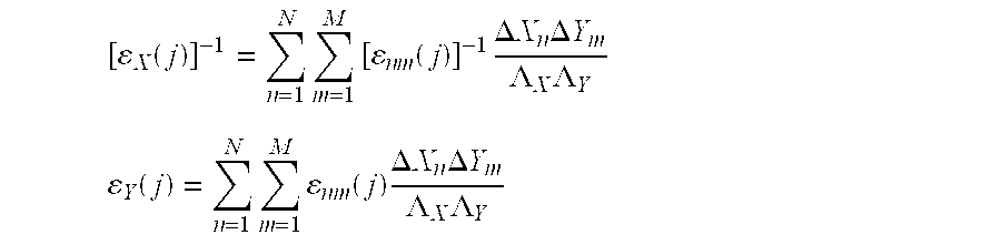
If the lines in the j-th layer area are parallel to the X-axis, we have: 
In the above equations, N is the number of stacks extending along the X-axis; M is the number of stacks extending along the Y-axis; ΔXn is the width of the n-th stack along the X-axis; ΔYm is the width of the m-th stack along the Y-axis; εnm(j) is the permittivity of a cell in the j-th layer, the cell belonging to the n-th stack along the X-axis and the m-th stack along the Y-axis; ΛX and ΛY are the pitches along the X-axis and Y-axis, respectively.
The structure pitches ΛY and ΛX are determined as follows: 
For the specific example of FIGS. 13A-13B, we have: N=2; M=2; ΔX1=0.3 nm; ΔX20.2 nm; ΔY1=0.1 nm; ΔY2=0.1 nm; ΛX=ΔX1+ΔX2=0.5 nm; ΛY=ΔY1+ΔY2=0.2 nm
The total reflectivity RTOT has the following form: 
wherein ψ describes the polarization of light, the condition ψ=0 corresponding to light polarized along Y-axis, the condition ψ=1 corresponding to light polarized along the X-axis, the condition ψ=0.5 corresponding to unpolarized light.
The reflectivity amplitudes RX(j,n,m) and RY(j,n,m) from different two-dimensional stacks (n,m) can be calculated using the above equations, but with the permittivities εX(j,n,m) and εY(j,n,m), wherein index j describes the layer, indices n and m describe those stacks along the X- and Y-axes to which the (n,m)-substack belongs. The permittivities εX(j,n,m) and εY(j,n,m) are calculated as follows:
Thus, by taking into account the relation between the wavelength of incident light and the structure pitch, the mostly preferred optical model can be selected accordingly and applied to carry out measurements of the structure parameters.
Those skilled in the art will readily appreciate that many modifications and changes may be applied to the invention as hereinbefore exemplified without departing from its scope defined in and by the appended claims. For example, the patterned structure may comprise any number of cells, each cell being formed of any number of stacks. In the method claims that follow, characters, which are used to designate claim steps, are provided for convenience only and do not apply any particular order of performing the steps.
Claims (37)
1. A method for measuring at least one desired parameter of a patterned structure which represents a grid having at least one cycle formed of at least two locally adjacent elements having different optical properties in respect of incident radiation, the structure having a plurality of features defined by a certain process of its manufacturing, the method comprising the steps of:
a) providing an optical model, which is based on at least some of said features of the structure and on relation between wavelength range of the incident radiation to be used for measurements and pitch of the structure under measurements, and is capable of determining theoretical data representative of photometric intensities of light components of different wavelengths specularly reflected from the structure and of calculating said at least one desired parameter of the structure;
b) locating a measurement area for applying thereto spectrophotometric measurements, wherein said measurement area is a grid cycles containing area and is substantially larger than a surface area of the structure defined by one grid cycle;
c) applying the spectrophotometric measurements to said measurement area by illuminating it with incident radiation of a preset substantially wide wavelength range, detecting light component substantially specularly reflected from the measurement area, and obtaining measured data representative of photometric intensities of each wavelength within said wavelength range;
d) analyzing the measured data and the theoretical data and optimizing said optical model until said theoretical data satisfies a predetermined condition; and
e) upon detecting that the predetermined condition is satisfied, calculating said at least one parameter of the structure.
2. The method according to claim 1 , wherein said at least some features of the structure on which the optical model is based are available prior to measurements.
3. The method according to claim 1 , wherein said at least some features of the structure on which the optical model is based comprises nominal values of said desired parameters to be measured.
4. The method according to claim 1 , wherein said at least some features of the structure on which the optical model is based comprises materials forming each of said at least two elements.
5. The method according to claim 1 , wherein the step of providing the optical model comprises the step of:
estimating known optical effects, that may be produced in the structure in response to the incident radiation, and contribution of said optical effects into the detected light component.
6. The method according to claim 1 , wherein said analyzing comprises the step of:
comparing the theoretical data with the measured data and providing data indicative of the relationship between the measured and theoretical data.
7. The method according to claim 1 , wherein said optimizing comprises the steps of:
adjusting certain variable factors of the optical model until the theoretical data satisfies the predetermined condition and obtaining correct values of the optical model factors.
8. The method according to claim 7 , wherein said certain variable factors of the optical model define contributions of known optical effects into the detected light component.
9. The method according to claim 1 , wherein said predetermined condition represents a merit function defining a certain value of a goodness of fit between the measured and theoretical data.
10. The method according to claim 1 , wherein said optimizing comprises the step of: varying a value of said at least one desired parameter until the theoretical data satisfies the predetermine condition.
11. The method according to claim 1 , wherein the measurement area is a part of the structure to be measured.
12. The method according to claim 1 , wherein the measurement area is located on a test site representing a test pattern similar to that of the structure, the test pattern having the same design rules and layer stacks.
13. The method according to claim 1 , wherein said structure is composed of n locally adjacent elements with j layers, and said photometric intensities obtained with the theoretical data are functions of effective permittivity ε of the structure.
14. The method according to claim 13 , wherein said theoretical data is determined according to the following equation:
wherein ψ describes the polarization of light: ψ=0 for light polarized along the Y-axis, ψ=1 for light polarized along the X-axis, ψ=0.5 for unpolarized light; RX(0) and RY(0) are reflectivity amplitudes of the entire structure along the X- and Y-axis, respectively.
15. The method according to claim 14 , wherein the effective permittivity is described by the following tensor: 
wherein tensor components εX(j) and εY(j) correspond to electric field vector parallel to the X-axis and Y-axis, respectively, and are as follows: 
wherein εn(j) is the permittivity of j-th layer in n-th stack; ΔXn is the width of the n-th stack; N is the number of stacks.
16. The method according to claim 15 , wherein said reflectivity amplitudes are determined by recurrent utilizing said tensor components.
17. The method according to claim 13 , wherein the effective permittivity is described by the following tensor: 
wherein tensor components εX(j, n) and εY(j, n) are as follows:
wherein α(λ) is the coefficient presenting a monotonically decreasing function of wavelength of incident radiation λ; α=0 when the structure pitch Λ is smaller than the wavelength of incident light λ, and α=1 when the structure pitch Λ is larger than the wavelength of incident light λ, and 0<α<1 when Λ˜λ.
18. The method according to claim 17 , wherein said theoretical data is determined according to the following equation: 
wherein ψ describes the polarization of light: ψ=0 for light polarized along the Y-axis, ψ=1 for light polarized along the X-axis, ψ=0.5 for unpolarized light; N is the number of stacks; RX(0,n) and RY(0,n) are the reflectivity amplitudes for entire n-th stack.
19. The method according to claim 18 , wherein said reflectivity amplitudes are determined by recurrent equations utilizing said tensor components.
20. The method according to claim 13 , wherein said at least one cycle is two-dimensional formed by said n different locally adjacent elements aligned along X-axis, and m different locally adjacent elements aligned along Y-axis.
21. The method according to claim 20 , wherein said theoretical data being determined by the following equation: 
wherein ψ describes the polarization of light, the condition ψ=0 corresponding to light polarized along the Y-axis, the condition ψ=1 corresponding to light polarized along the X-axis, the condition ψ=0.5 corresponding to unpolarized light; RX(0,n,m) and RY(0,n,m) are reflectivity amplitudes from all different two-dimensional elements of the structure.
22. The method according to claim 21 , wherein said reflectivity amplitudes are determines by recurrent equations utilizing components of the effective permittivity tensor εX(j,n,m) and εY(j,n,m), which are as follows:
23. The method according to claim 1 , wherein said at least one desired parameter to be measured is a width of at least one of said at least two locally adjacent elements in the grid cycle.
24. The method according to claim 1 , wherein said at least one desired parameter to be measured is a depth of at least one layer of said at least one stack.
25. The method according to claim 1 , wherein said at least one desired parameter to be measured is a depth of a metal-loss portion resulting from a chemical mechanical polishing applied to said structure.
26. The method according to claim 1 , wherein said patterned structure is a semiconductor wafer.
27. The method according to claim 1 , wherein said manufacturing process of Chemical Mechanical Planarization (CMP).
28. An apparatus for measuring at least one desired parameter of a patterned structure that represents a grid having at least one grid cycle formed of at least two locally adjacent elements having different optical properties in respect of an incident radiation, the structure having a plurality of features defined by a certain process of its manufacturing, the apparatus comprising:
a spectrophotometer illuminating a measurement area by an incident radiation of a preset substantially wide wavelength range and detecting a specular reflection light component of light reflected from the measurement area for providing measured data representative of photometric intensities of detected light within said wavelength range, wherein the measurement area is substantially larger than a surface area of the structure defined by the grid cycle; and
a processor unit coupled to the spectrophotometer, the processor unit comprising a pattern recognition software and a translation means so as to be responsive to said measured data and locate measurements, the processor being operable for
applying an optical model, based on at least some of said features of the structure and on relation between wavelength range of the incident radiation to be used for measurements and pitch of the structure under measurements, for providing theoretical data representative of photometric intensities of light specularly reflected from the structure within said wavelength range and calculating said at least one desired parameter, and
comparing said measured and theoretical data and detecting whether the theoretical data satisfies a predetermined condition.
29. The apparatus according to claim 28 , wherein said spectrophotometer comprises a spectrophotometric detector and a variable aperture stop located in the optical path of light reaching the detector, the diameter of the aperture stop being variable in accordance with the grid cycle of the measured structure.
30. The apparatus according to claim 28 , wherein said measurement area is located within the patterned area of said structure.
31. The apparatus according to claim 28 , wherein said measurement area is located within a test site located outside the patterned area of said structure.
32. The apparatus according to claim 28 , wherein each of said at least two elements is a stack including layers having different optical properties.
33. The apparatus according to claim 28 , wherein said at least one desired parameter to be measured is a width of at least one of said at least two locally adjacent elements in the grid cycle.
34. The apparatus according to claim 32 , wherein said at least one desired parameter to be measured is a depth of at least one layer of said at least one stack.
35. The apparatus according to claim 32 , wherein said at least one desired parameter to be measured is a depth of a metal-loss portion resulting from a chemical mechanical polishing applied to said structure.
36. A working station for processing wafers progressing on a production line, wherein each of said wafers is a patterned structure that represents a grid having at least one grid cycle formed of at least two locally adjacent elements having different optical properties in respect of an incident radiation, and the structure has a plurality of features defined by a certain process of its manufacturing, the working station comprising an inspection apparatus and a support frame for supporting the wafer within an inspection plane, wherein the inspection apparatus comprises:
a spectrophotometer illuminating a measurement area by an incident radiation of a preset substantially wide wavelength range and detecting a specular reflection light component of light reflected from the measurement area for providing measured data representative of photometric intensities of detected light within said wavelength range, wherein the measurement area is substantially larger than a surface area of the structure defined by the grid cycle; and
a processor unit coupled to the spectrophotometer, the processor unit comprising a pattern recognition software and a translation means so as to be responsive to said measured data and locate measurements, the processor being operable for
applying an optical model, based on at least some of said features of the structure and on relation between wavelength range of the incident radiation to be used for measurements and pitch of the structure under measurements, for providing theoretical data representative of photometric intensities of light specularly reflected from the structure within said wavelength range and calculating said at least one desired parameter, and
comparing said measured and theoretical data and detecting whether the theoretical data satisfies a predetermined condition.
37. The working station according to claim 36 , wherein said production line comprises a Chemical Mechanical Planarization (CMP) tools arrangement.
Priority Applications (4)
| Application Number | Priority Date | Filing Date | Title |
|---|---|---|---|
| US09/605,664 US6476920B1 (en) | 1998-03-18 | 2000-06-26 | Method and apparatus for measurements of patterned structures |
| US10/011,263 US6836324B2 (en) | 1998-03-18 | 2001-11-13 | Method and apparatus for measurements of patterned structures |
| US10/919,823 US7123366B2 (en) | 1998-03-18 | 2004-08-17 | Method and apparatus for measurements of patterned structures |
| US11/053,254 US7187456B2 (en) | 1998-03-18 | 2005-02-08 | Method and apparatus for measurements of patterned structures |
Applications Claiming Priority (5)
| Application Number | Priority Date | Filing Date | Title |
|---|---|---|---|
| IL123727 | 1998-03-18 | ||
| IL12372798A IL123727A (en) | 1998-03-18 | 1998-03-18 | Method and apparatus for measurement of patterned structures |
| US9237898A | 1998-06-05 | 1998-06-05 | |
| US09/267,989 US6100985A (en) | 1998-03-18 | 1999-03-12 | Method and apparatus for measurements of patterned structures |
| US09/605,664 US6476920B1 (en) | 1998-03-18 | 2000-06-26 | Method and apparatus for measurements of patterned structures |
Related Parent Applications (1)
| Application Number | Title | Priority Date | Filing Date |
|---|---|---|---|
| US09/267,989 Continuation-In-Part US6100985A (en) | 1998-03-18 | 1999-03-12 | Method and apparatus for measurements of patterned structures |
Related Child Applications (1)
| Application Number | Title | Priority Date | Filing Date |
|---|---|---|---|
| US10/011,263 Continuation-In-Part US6836324B2 (en) | 1998-03-18 | 2001-11-13 | Method and apparatus for measurements of patterned structures |
Publications (1)
| Publication Number | Publication Date |
|---|---|
| US6476920B1 true US6476920B1 (en) | 2002-11-05 |
Family
ID=27271853
Family Applications (1)
| Application Number | Title | Priority Date | Filing Date |
|---|---|---|---|
| US09/605,664 Expired - Lifetime US6476920B1 (en) | 1998-03-18 | 2000-06-26 | Method and apparatus for measurements of patterned structures |
Country Status (1)
| Country | Link |
|---|---|
| US (1) | US6476920B1 (en) |
Cited By (49)
| Publication number | Priority date | Publication date | Assignee | Title |
|---|---|---|---|---|
| US20020033450A1 (en) * | 2000-08-31 | 2002-03-21 | Nova Measuring Instruments Ltd. | Method and system for optical inspection of a structure formed with a surface relief |
| US20020102749A1 (en) * | 2000-09-20 | 2002-08-01 | John Fielden | Methods and systems for determining a characteristic of a layer formed on a specimen by a deposition process |
| US20020128784A1 (en) * | 1998-03-18 | 2002-09-12 | David Scheiner | Method and apparatus for measurements of patterned structures |
| US20020180961A1 (en) * | 2000-09-20 | 2002-12-05 | Dan Wack | Methods and systems for determining an adhesion characteristic and a thickness of a specimen |
| US20020180986A1 (en) * | 2000-09-20 | 2002-12-05 | Mehrdad Nikoonahad | Methods and systems for determining a critical dimension, a presence of defects, and a thin film characteristic of a specimen |
| US20030002043A1 (en) * | 2001-04-10 | 2003-01-02 | Kla-Tencor Corporation | Periodic patterns and technique to control misalignment |
| WO2003014866A2 (en) * | 2001-08-06 | 2003-02-20 | Timbre Technologies, Inc. | Method and system for dynamic learning through a regression-based library generation process |
| US20030071994A1 (en) * | 2001-10-09 | 2003-04-17 | Peter G. Borden | Calibration as well as measurement on the same workpiece during fabrication |
| US20030081216A1 (en) * | 2001-11-01 | 2003-05-01 | Martin Ebert | Graphical user interface for sample positioning |
| US20030148198A1 (en) * | 2000-05-04 | 2003-08-07 | Suresh Lakkapragada | Methods and systems for lithography process control |
| US6660542B1 (en) * | 2001-04-06 | 2003-12-09 | Advanced Micro Devices, Inc. | Method of controlling stepper process parameters based upon optical properties of incoming process layers, and system for accomplishing same |
| US6673637B2 (en) | 2000-09-20 | 2004-01-06 | Kla-Tencor Technologies | Methods and systems for determining a presence of macro defects and overlay of a specimen |
| US6694284B1 (en) | 2000-09-20 | 2004-02-17 | Kla-Tencor Technologies Corp. | Methods and systems for determining at least four properties of a specimen |
| US20040032582A1 (en) * | 2002-07-01 | 2004-02-19 | Johnson Kenneth C. | Reduced multicubic database interpolation method for optical measurement of diffractive microstructures |
| US6713753B1 (en) | 2001-07-03 | 2004-03-30 | Nanometrics Incorporated | Combination of normal and oblique incidence polarimetry for the characterization of gratings |
| WO2004027439A1 (en) * | 2002-09-23 | 2004-04-01 | Boxer Cross Inc. | Measurement of lateral diffusion of diffused layers. |
| US6768967B2 (en) * | 2000-08-10 | 2004-07-27 | Therma-Wave, Inc. | Database interpolation method for optical measurement of diffractive microstructures |
| US6782337B2 (en) | 2000-09-20 | 2004-08-24 | Kla-Tencor Technologies Corp. | Methods and systems for determining a critical dimension an a presence of defects on a specimen |
| US20040169861A1 (en) * | 2002-12-05 | 2004-09-02 | Kla-Tenor Technologies Corporation | Apparatus and method for detecting overlay errors using scatterometry |
| US6812045B1 (en) | 2000-09-20 | 2004-11-02 | Kla-Tencor, Inc. | Methods and systems for determining a characteristic of a specimen prior to, during, or subsequent to ion implantation |
| US20050088187A1 (en) * | 2001-03-05 | 2005-04-28 | Applied Materials, Inc. | Use of coefficient of a power curve to evaluate a semiconductor wafer |
| US20050095727A1 (en) * | 2003-11-05 | 2005-05-05 | Weng Chang | Test region layout for shallow trench isolation |
| US6898537B1 (en) | 2001-04-27 | 2005-05-24 | Nanometrics Incorporated | Measurement of diffracting structures using one-half of the non-zero diffracted orders |
| US20050195398A1 (en) * | 2002-12-05 | 2005-09-08 | Kla-Tencor Technologies Corporation | Continuously varying offset mark and methods of determining overlay |
| US6949462B1 (en) | 2002-04-04 | 2005-09-27 | Nanometrics Incorporated | Measuring an alignment target with multiple polarization states |
| US6982793B1 (en) | 2002-04-04 | 2006-01-03 | Nanometrics Incorporated | Method and apparatus for using an alignment target with designed in offset |
| US6992764B1 (en) | 2002-09-30 | 2006-01-31 | Nanometrics Incorporated | Measuring an alignment target with a single polarization state |
| US7061615B1 (en) | 2001-09-20 | 2006-06-13 | Nanometrics Incorporated | Spectroscopically measured overlay target |
| US20060132808A1 (en) * | 2004-12-21 | 2006-06-22 | Honeywell International Inc. | Thin thickness measurement method and apparatus |
| US7115858B1 (en) | 2000-09-25 | 2006-10-03 | Nanometrics Incorporated | Apparatus and method for the measurement of diffracting structures |
| US20060232768A1 (en) * | 2002-03-01 | 2006-10-19 | Borden Peter G | Evaluating a multi-layered structure for voids |
| US7212293B1 (en) | 2004-06-01 | 2007-05-01 | N&K Technology, Inc. | Optical determination of pattern feature parameters using a scalar model having effective optical properties |
| US20070105029A1 (en) * | 2003-12-19 | 2007-05-10 | International Business Machines Corporation | Differential critical dimension and overlay metrology apparatus and measurement method |
| US7235474B1 (en) * | 2004-05-04 | 2007-06-26 | Advanced Micro Devices, Inc. | System and method for imprint lithography to facilitate dual damascene integration with two imprint acts |
| US20070153277A1 (en) * | 2005-12-29 | 2007-07-05 | Honeywell International Inc. | Color sensor |
| US20070178611A1 (en) * | 2006-01-30 | 2007-08-02 | Shoaib Zaidi | Semiconductor wafer having measurement area feature for determining dielectric layer thickness |
| US7262864B1 (en) * | 2001-07-02 | 2007-08-28 | Advanced Micro Devices, Inc. | Method and apparatus for determining grid dimensions using scatterometry |
| US20070292778A1 (en) * | 2006-06-15 | 2007-12-20 | Bang Kyoung-Yoon | Methods of measuring critical dimensions and related devices |
| US20080037005A1 (en) * | 2005-01-12 | 2008-02-14 | Noah Bareket | System for measuring a sample with a layer containing a periodic diffracting structure |
| US20080157013A1 (en) * | 2006-12-27 | 2008-07-03 | Honeywell International Inc. | System and method for z-structure measurements using simultaneous multi-band tomography |
| US7751046B2 (en) | 2000-09-20 | 2010-07-06 | Kla-Tencor Technologies Corp. | Methods and systems for determining a critical dimension and overlay of a specimen |
| US7859659B2 (en) | 1998-03-06 | 2010-12-28 | Kla-Tencor Corporation | Spectroscopic scatterometer system |
| US8017927B2 (en) | 2005-12-16 | 2011-09-13 | Honeywell International Inc. | Apparatus, system, and method for print quality measurements using multiple adjustable sensors |
| US8401809B2 (en) | 2010-07-12 | 2013-03-19 | Honeywell International Inc. | System and method for adjusting an on-line appearance sensor system |
| US8618929B2 (en) | 2011-05-09 | 2013-12-31 | Honeywell International Inc. | Wireless conveyor belt condition monitoring system and related apparatus and method |
| USRE45245E1 (en) | 2000-08-30 | 2014-11-18 | Kla-Tencor Corporation | Apparatus and methods for determining overlay of structures having rotational or mirror symmetry |
| US10451412B2 (en) | 2016-04-22 | 2019-10-22 | Kla-Tencor Corporation | Apparatus and methods for detecting overlay errors using scatterometry |
| US10705437B2 (en) | 2017-10-10 | 2020-07-07 | Asml Netherlands B.V | Metrology method and apparatus, computer program and lithographic system |
| US11320732B2 (en) | 2020-03-19 | 2022-05-03 | Sk Hynix Inc | Method of measuring critical dimension of a three-dimensional structure and apparatus for measuring the same |
Citations (18)
| Publication number | Priority date | Publication date | Assignee | Title |
|---|---|---|---|---|
| US4555767A (en) | 1982-05-27 | 1985-11-26 | International Business Machines Corporation | Method and apparatus for measuring thickness of epitaxial layer by infrared reflectance |
| US4740082A (en) | 1983-08-30 | 1988-04-26 | The Perkin-Elmer Corporation | Spectrophotometer |
| US4899055A (en) | 1988-05-12 | 1990-02-06 | Tencor Instruments | Thin film thickness measuring method |
| US4999014A (en) | 1989-05-04 | 1991-03-12 | Therma-Wave, Inc. | Method and apparatus for measuring thickness of thin films |
| US4999508A (en) | 1988-12-29 | 1991-03-12 | Olympus Optical Co., Ltd. | Optical film thickness measuring device for measuring two-layer film thicknesses using spectral reflectance |
| US5087121A (en) | 1987-12-01 | 1992-02-11 | Canon Kabushiki Kaisha | Depth/height measuring device |
| US5361137A (en) | 1992-08-31 | 1994-11-01 | Texas Instruments Incorporated | Process control for submicron linewidth measurement |
| US5450205A (en) | 1993-05-28 | 1995-09-12 | Massachusetts Institute Of Technology | Apparatus and method for real-time measurement of thin film layer thickness and changes thereof |
| US5517312A (en) | 1993-11-09 | 1996-05-14 | Nova Measuring Instruments, Ltd. | Device for measuring the thickness of thin films |
| US5571312A (en) | 1992-07-28 | 1996-11-05 | Cresco Inc., Sa. | Environmentally safe epoxy adhesive-copper hull coating and method |
| US5604581A (en) | 1994-10-07 | 1997-02-18 | On-Line Technologies, Inc. | Film thickness and free carrier concentration analysis method and apparatus |
| US5702956A (en) | 1996-08-26 | 1997-12-30 | Taiwan Semiconductor Manufactoring, Company Ltd | Test site and a method of monitoring via etch depths for semiconductor devices |
| US5867276A (en) | 1997-03-07 | 1999-02-02 | Bio-Rad Laboratories, Inc. | Method for broad wavelength scatterometry |
| US5898500A (en) | 1997-02-26 | 1999-04-27 | Instruments, S.A. | Device and method for three-dimensional measurements and observation in situ of a surface layer deposited on a thin-film stack |
| US5900633A (en) | 1997-12-15 | 1999-05-04 | On-Line Technologies, Inc | Spectrometric method for analysis of film thickness and composition on a patterned sample |
| US5946102A (en) | 1997-07-28 | 1999-08-31 | Mmr Technologies, Inc. | Method and apparatus for parameter difference imaging of a sample surface |
| US5959731A (en) | 1996-05-03 | 1999-09-28 | Virginia Semiconductor, Inc. | Optical micrometer for measuring thickness of transparent substrates based on optical absorption |
| US6100985A (en) * | 1998-03-18 | 2000-08-08 | Nova Measuring Instruments, Ltd. | Method and apparatus for measurements of patterned structures |
-
2000
- 2000-06-26 US US09/605,664 patent/US6476920B1/en not_active Expired - Lifetime
Patent Citations (18)
| Publication number | Priority date | Publication date | Assignee | Title |
|---|---|---|---|---|
| US4555767A (en) | 1982-05-27 | 1985-11-26 | International Business Machines Corporation | Method and apparatus for measuring thickness of epitaxial layer by infrared reflectance |
| US4740082A (en) | 1983-08-30 | 1988-04-26 | The Perkin-Elmer Corporation | Spectrophotometer |
| US5087121A (en) | 1987-12-01 | 1992-02-11 | Canon Kabushiki Kaisha | Depth/height measuring device |
| US4899055A (en) | 1988-05-12 | 1990-02-06 | Tencor Instruments | Thin film thickness measuring method |
| US4999508A (en) | 1988-12-29 | 1991-03-12 | Olympus Optical Co., Ltd. | Optical film thickness measuring device for measuring two-layer film thicknesses using spectral reflectance |
| US4999014A (en) | 1989-05-04 | 1991-03-12 | Therma-Wave, Inc. | Method and apparatus for measuring thickness of thin films |
| US5571312A (en) | 1992-07-28 | 1996-11-05 | Cresco Inc., Sa. | Environmentally safe epoxy adhesive-copper hull coating and method |
| US5361137A (en) | 1992-08-31 | 1994-11-01 | Texas Instruments Incorporated | Process control for submicron linewidth measurement |
| US5450205A (en) | 1993-05-28 | 1995-09-12 | Massachusetts Institute Of Technology | Apparatus and method for real-time measurement of thin film layer thickness and changes thereof |
| US5517312A (en) | 1993-11-09 | 1996-05-14 | Nova Measuring Instruments, Ltd. | Device for measuring the thickness of thin films |
| US5604581A (en) | 1994-10-07 | 1997-02-18 | On-Line Technologies, Inc. | Film thickness and free carrier concentration analysis method and apparatus |
| US5959731A (en) | 1996-05-03 | 1999-09-28 | Virginia Semiconductor, Inc. | Optical micrometer for measuring thickness of transparent substrates based on optical absorption |
| US5702956A (en) | 1996-08-26 | 1997-12-30 | Taiwan Semiconductor Manufactoring, Company Ltd | Test site and a method of monitoring via etch depths for semiconductor devices |
| US5898500A (en) | 1997-02-26 | 1999-04-27 | Instruments, S.A. | Device and method for three-dimensional measurements and observation in situ of a surface layer deposited on a thin-film stack |
| US5867276A (en) | 1997-03-07 | 1999-02-02 | Bio-Rad Laboratories, Inc. | Method for broad wavelength scatterometry |
| US5946102A (en) | 1997-07-28 | 1999-08-31 | Mmr Technologies, Inc. | Method and apparatus for parameter difference imaging of a sample surface |
| US5900633A (en) | 1997-12-15 | 1999-05-04 | On-Line Technologies, Inc | Spectrometric method for analysis of film thickness and composition on a patterned sample |
| US6100985A (en) * | 1998-03-18 | 2000-08-08 | Nova Measuring Instruments, Ltd. | Method and apparatus for measurements of patterned structures |
Non-Patent Citations (1)
| Title |
|---|
| Y. Ushio et al.; "In-Situ Monitoring of CMP Process Utilizing 0-Order Spectrometry"; CMP-MIC Conferences, Feb. 11-12, 1999, pp. 23-29. |
Cited By (140)
| Publication number | Priority date | Publication date | Assignee | Title |
|---|---|---|---|---|
| US7859659B2 (en) | 1998-03-06 | 2010-12-28 | Kla-Tencor Corporation | Spectroscopic scatterometer system |
| US7898661B2 (en) | 1998-03-06 | 2011-03-01 | Kla-Tencor Corporation | Spectroscopic scatterometer system |
| US7123366B2 (en) | 1998-03-18 | 2006-10-17 | Nova Measuring Instruments Ltd. | Method and apparatus for measurements of patterned structures |
| US6836324B2 (en) * | 1998-03-18 | 2004-12-28 | Nova Measuring Instruments Ltd. | Method and apparatus for measurements of patterned structures |
| US20020128784A1 (en) * | 1998-03-18 | 2002-09-12 | David Scheiner | Method and apparatus for measurements of patterned structures |
| US20050062965A1 (en) * | 1998-03-18 | 2005-03-24 | Nova Measuring Instruments Ltd | Method and apparatus for measurements of patterned structures |
| US20050146729A1 (en) * | 1998-03-18 | 2005-07-07 | Nova Measuring Instruments Ltd. | Method and appratus for measurements of patterned structures |
| US7187456B2 (en) | 1998-03-18 | 2007-03-06 | Nova Measuring Instruments Ltd. | Method and apparatus for measurements of patterned structures |
| US6987572B2 (en) | 2000-05-04 | 2006-01-17 | Kla-Tencor Technologies Corp. | Methods and systems for lithography process control |
| US7767956B2 (en) | 2000-05-04 | 2010-08-03 | Kla-Tencor Technologies Corp. | Methods and systems for lithography process control |
| US20030148198A1 (en) * | 2000-05-04 | 2003-08-07 | Suresh Lakkapragada | Methods and systems for lithography process control |
| US7462814B2 (en) | 2000-05-04 | 2008-12-09 | Kla-Tencor Technologies Corp. | Methods and systems for lithography process control |
| US20090079974A1 (en) * | 2000-05-04 | 2009-03-26 | Kla-Tencor Technologies Corporation | Methods and systems for lithography process control |
| US20060138366A1 (en) * | 2000-05-04 | 2006-06-29 | Kla-Tencor Technologies Corp. | Methods and systems for lithography process control |
| US20040005507A1 (en) * | 2000-05-04 | 2004-01-08 | Kla-Tencor, Inc. | Methods and systems for lithography process control |
| US6689519B2 (en) | 2000-05-04 | 2004-02-10 | Kla-Tencor Technologies Corp. | Methods and systems for lithography process control |
| US20050280832A1 (en) * | 2000-08-10 | 2005-12-22 | Johnson Kenneth C | Database interpolation method for optical measurement of diffractive microstructures |
| US6950780B2 (en) | 2000-08-10 | 2005-09-27 | Tokyo Electron Limited | Database interpolation method for optical measurement of diffractive microstructures |
| US20040167722A1 (en) * | 2000-08-10 | 2004-08-26 | Johnson Kenneth C. | Database interpolation method for optical measurement of diffractive microstructures |
| US7069182B2 (en) | 2000-08-10 | 2006-06-27 | Tokyo Electron Limited | Database interpolation method for optical measurement of diffractive microstructures |
| US6768967B2 (en) * | 2000-08-10 | 2004-07-27 | Therma-Wave, Inc. | Database interpolation method for optical measurement of diffractive microstructures |
| USRE45245E1 (en) | 2000-08-30 | 2014-11-18 | Kla-Tencor Corporation | Apparatus and methods for determining overlay of structures having rotational or mirror symmetry |
| US9182680B2 (en) | 2000-08-30 | 2015-11-10 | Kla-Tencor Corporation | Apparatus and methods for determining overlay of structures having rotational or mirror symmetry |
| US9347879B2 (en) | 2000-08-30 | 2016-05-24 | Kla-Tencor Corporation | Apparatus and methods for detecting overlay errors using scatterometry |
| US9702693B2 (en) | 2000-08-30 | 2017-07-11 | Kla-Tencor Corporation | Apparatus for measuring overlay errors |
| US6720568B2 (en) * | 2000-08-31 | 2004-04-13 | Nova Measuring Instruments Ltd. | Method and system for optical inspection of a structure formed with a surface relief |
| US20020033450A1 (en) * | 2000-08-31 | 2002-03-21 | Nova Measuring Instruments Ltd. | Method and system for optical inspection of a structure formed with a surface relief |
| US20020180986A1 (en) * | 2000-09-20 | 2002-12-05 | Mehrdad Nikoonahad | Methods and systems for determining a critical dimension, a presence of defects, and a thin film characteristic of a specimen |
| US6673637B2 (en) | 2000-09-20 | 2004-01-06 | Kla-Tencor Technologies | Methods and systems for determining a presence of macro defects and overlay of a specimen |
| US6782337B2 (en) | 2000-09-20 | 2004-08-24 | Kla-Tencor Technologies Corp. | Methods and systems for determining a critical dimension an a presence of defects on a specimen |
| US20020102749A1 (en) * | 2000-09-20 | 2002-08-01 | John Fielden | Methods and systems for determining a characteristic of a layer formed on a specimen by a deposition process |
| US20020180961A1 (en) * | 2000-09-20 | 2002-12-05 | Dan Wack | Methods and systems for determining an adhesion characteristic and a thickness of a specimen |
| US6818459B2 (en) | 2000-09-20 | 2004-11-16 | Kla-Tencor Technologies Corp. | Methods and systems for determining a presence of macro defects and overlay of a specimen |
| US6694284B1 (en) | 2000-09-20 | 2004-02-17 | Kla-Tencor Technologies Corp. | Methods and systems for determining at least four properties of a specimen |
| US7751046B2 (en) | 2000-09-20 | 2010-07-06 | Kla-Tencor Technologies Corp. | Methods and systems for determining a critical dimension and overlay of a specimen |
| US6812045B1 (en) | 2000-09-20 | 2004-11-02 | Kla-Tencor, Inc. | Methods and systems for determining a characteristic of a specimen prior to, during, or subsequent to ion implantation |
| US6806951B2 (en) | 2000-09-20 | 2004-10-19 | Kla-Tencor Technologies Corp. | Methods and systems for determining at least one characteristic of defects on at least two sides of a specimen |
| US8179530B2 (en) | 2000-09-20 | 2012-05-15 | Kla-Tencor Technologies Corp. | Methods and systems for determining a critical dimension and overlay of a specimen |
| US20020188417A1 (en) * | 2000-09-20 | 2002-12-12 | Ady Levy | Methods and systems for determining a property of a specimen prior to, during, or subsequent to an etch process |
| US8502979B2 (en) | 2000-09-20 | 2013-08-06 | Kla-Tencor Technologies Corp. | Methods and systems for determining a critical dimension and overlay of a specimen |
| US6829559B2 (en) | 2000-09-20 | 2004-12-07 | K.L.A.-Tencor Technologies | Methods and systems for determining a presence of macro and micro defects on a specimen |
| US7115858B1 (en) | 2000-09-25 | 2006-10-03 | Nanometrics Incorporated | Apparatus and method for the measurement of diffracting structures |
| US7372565B1 (en) | 2000-09-25 | 2008-05-13 | Nanometrics Incorporated | Spectrometer measurement of diffracting structures |
| US7130055B2 (en) | 2001-03-05 | 2006-10-31 | Applied Materials, Inc. | Use of coefficient of a power curve to evaluate a semiconductor wafer |
| US20050088187A1 (en) * | 2001-03-05 | 2005-04-28 | Applied Materials, Inc. | Use of coefficient of a power curve to evaluate a semiconductor wafer |
| US6660542B1 (en) * | 2001-04-06 | 2003-12-09 | Advanced Micro Devices, Inc. | Method of controlling stepper process parameters based upon optical properties of incoming process layers, and system for accomplishing same |
| US20060262326A1 (en) * | 2001-04-10 | 2006-11-23 | Ibrahim Abdulhalim | Periodic patterns and technique to control misalignment between two layers |
| US9234745B2 (en) | 2001-04-10 | 2016-01-12 | Kla-Tencor Corporation | Periodic patterns and techniques to control misalignment between two layers |
| US20050157297A1 (en) * | 2001-04-10 | 2005-07-21 | Ibrahim Abdulhalim | Periodic patterns and technique to control misalignment between two layers |
| US10151584B2 (en) | 2001-04-10 | 2018-12-11 | Kla-Tencor Corporation | Periodic patterns and technique to control misalignment between two layers |
| US20040229471A1 (en) * | 2001-04-10 | 2004-11-18 | Ibrahim Abdulhalim | Periodic patterns and technique to control misalignment between two layers |
| US8570515B2 (en) | 2001-04-10 | 2013-10-29 | Kla-Tencor Corporation | Periodic patterns and technique to control misalignment between two layers |
| US7656528B2 (en) | 2001-04-10 | 2010-02-02 | Kla-Tencor Corporation | Periodic patterns and technique to control misalignment between two layers |
| US20050208685A1 (en) * | 2001-04-10 | 2005-09-22 | Ibrahim Abdulhalim | Periodic patterns and technique to control misalignment |
| US9835447B2 (en) | 2001-04-10 | 2017-12-05 | Kla-Tencor Corporation | Periodic patterns and technique to control misalignment between two layers |
| US9476698B2 (en) | 2001-04-10 | 2016-10-25 | Kla-Tencor Corporation | Periodic patterns and technique to control misalignment between two layers |
| US20030002043A1 (en) * | 2001-04-10 | 2003-01-02 | Kla-Tencor Corporation | Periodic patterns and technique to control misalignment |
| US9103662B2 (en) | 2001-04-10 | 2015-08-11 | Kla-Tencor Corporation | Periodic patterns and technique to control misalignment between two layers |
| US20060132807A1 (en) * | 2001-04-10 | 2006-06-22 | Ibrahim Abdulhalim | Periodic patterns and technique to control misalignment between two layers |
| US20060065625A1 (en) * | 2001-04-10 | 2006-03-30 | Ibrahim Abdulhalim | Periodic patterns and technique to control misalignment between two layers |
| US8525994B2 (en) | 2001-04-10 | 2013-09-03 | Kla-Tencor Corporation | Periodic patterns and technique to control misaligment between two layers |
| US20040061857A1 (en) * | 2001-04-10 | 2004-04-01 | Ibrahim Abdulhalim | Periodic patterns and technique to control misalignment between two layers |
| US6898537B1 (en) | 2001-04-27 | 2005-05-24 | Nanometrics Incorporated | Measurement of diffracting structures using one-half of the non-zero diffracted orders |
| US7262864B1 (en) * | 2001-07-02 | 2007-08-28 | Advanced Micro Devices, Inc. | Method and apparatus for determining grid dimensions using scatterometry |
| US6713753B1 (en) | 2001-07-03 | 2004-03-30 | Nanometrics Incorporated | Combination of normal and oblique incidence polarimetry for the characterization of gratings |
| WO2003014866A2 (en) * | 2001-08-06 | 2003-02-20 | Timbre Technologies, Inc. | Method and system for dynamic learning through a regression-based library generation process |
| US6785638B2 (en) * | 2001-08-06 | 2004-08-31 | Timbre Technologies, Inc. | Method and system of dynamic learning through a regression-based library generation process |
| US6928395B2 (en) | 2001-08-06 | 2005-08-09 | Timbre Technologies, Inc. | Method and system for dynamic learning through a regression-based library generation process |
| US20040220760A1 (en) * | 2001-08-06 | 2004-11-04 | Timbre Technologies, Inc. | Method and system of dynamic learning through a regression-based library generation process |
| WO2003014866A3 (en) * | 2001-08-06 | 2003-10-16 | Timbre Tech Inc | Method and system for dynamic learning through a regression-based library generation process |
| US20040225477A1 (en) * | 2001-08-06 | 2004-11-11 | Timbre Technologies, Inc. | Method and system of dynamic learning through a regression-based library generation process |
| US6961679B2 (en) | 2001-08-06 | 2005-11-01 | Timbre Technologies, Inc. | Method and system of dynamic learning through a regression-based library generation process |
| US7061615B1 (en) | 2001-09-20 | 2006-06-13 | Nanometrics Incorporated | Spectroscopically measured overlay target |
| US20030071994A1 (en) * | 2001-10-09 | 2003-04-17 | Peter G. Borden | Calibration as well as measurement on the same workpiece during fabrication |
| US6940592B2 (en) | 2001-10-09 | 2005-09-06 | Applied Materials, Inc. | Calibration as well as measurement on the same workpiece during fabrication |
| US20050264806A1 (en) * | 2001-10-09 | 2005-12-01 | Borden Peter G | Calibration as well as measurement on the same workpiece during fabrication |
| US20030081216A1 (en) * | 2001-11-01 | 2003-05-01 | Martin Ebert | Graphical user interface for sample positioning |
| US7301619B2 (en) * | 2002-03-01 | 2007-11-27 | Applied Materials, Inc. | Evaluating a multi-layered structure for voids |
| US20060232768A1 (en) * | 2002-03-01 | 2006-10-19 | Borden Peter G | Evaluating a multi-layered structure for voids |
| US7236244B1 (en) | 2002-04-04 | 2007-06-26 | Nanometrics Incorporated | Alignment target to be measured with multiple polarization states |
| US7230705B1 (en) | 2002-04-04 | 2007-06-12 | Nanometrics Incorporated | Alignment target with designed in offset |
| US6949462B1 (en) | 2002-04-04 | 2005-09-27 | Nanometrics Incorporated | Measuring an alignment target with multiple polarization states |
| US6982793B1 (en) | 2002-04-04 | 2006-01-03 | Nanometrics Incorporated | Method and apparatus for using an alignment target with designed in offset |
| US7043397B2 (en) | 2002-07-01 | 2006-05-09 | Tokyo Electron Limited | Reduced multicubic database interpolation method for optical measurement of diffractive microstructures |
| US6947135B2 (en) * | 2002-07-01 | 2005-09-20 | Therma-Wave, Inc. | Reduced multicubic database interpolation method for optical measurement of diffractive microstructures |
| US20040032582A1 (en) * | 2002-07-01 | 2004-02-19 | Johnson Kenneth C. | Reduced multicubic database interpolation method for optical measurement of diffractive microstructures |
| US20050280810A1 (en) * | 2002-07-01 | 2005-12-22 | Johnson Kenneth C | Reduced multicubic database interpolation method for optical measurement of diffractive microstructures |
| US20040063225A1 (en) * | 2002-09-23 | 2004-04-01 | Borden Peter G. | Measurement of lateral diffusion of diffused layers |
| WO2004027439A1 (en) * | 2002-09-23 | 2004-04-01 | Boxer Cross Inc. | Measurement of lateral diffusion of diffused layers. |
| US6992764B1 (en) | 2002-09-30 | 2006-01-31 | Nanometrics Incorporated | Measuring an alignment target with a single polarization state |
| US7564557B2 (en) | 2002-12-05 | 2009-07-21 | Kla-Tencor Technologies Corp. | Apparatus and methods for detecting overlay errors using scatterometry |
| US7433040B2 (en) | 2002-12-05 | 2008-10-07 | Kla-Tencor Technologies Corp. | Apparatus and methods for detecting overlay errors using scatterometry |
| US20040169861A1 (en) * | 2002-12-05 | 2004-09-02 | Kla-Tenor Technologies Corporation | Apparatus and method for detecting overlay errors using scatterometry |
| US20050195398A1 (en) * | 2002-12-05 | 2005-09-08 | Kla-Tencor Technologies Corporation | Continuously varying offset mark and methods of determining overlay |
| US7933016B2 (en) | 2002-12-05 | 2011-04-26 | Kla-Tencor Technologies Corporation | Apparatus and methods for detecting overlay errors using scatterometry |
| US7317531B2 (en) | 2002-12-05 | 2008-01-08 | Kla-Tencor Technologies Corporation | Apparatus and methods for detecting overlay errors using scatterometry |
| US7876440B2 (en) | 2002-12-05 | 2011-01-25 | Kla-Tencor Technologies Corporation | Apparatus and methods for detecting overlay errors using scatterometry |
| US7663753B2 (en) | 2002-12-05 | 2010-02-16 | Kla-Tencor Technologies Corporation | Apparatus and methods for detecting overlay errors using scatterometry |
| US7440105B2 (en) | 2002-12-05 | 2008-10-21 | Kla-Tencor Technologies Corporation | Continuously varying offset mark and methods of determining overlay |
| US7289213B2 (en) | 2003-02-22 | 2007-10-30 | Kla-Tencor Technologies Corporation | Apparatus and methods for detecting overlay errors using scatterometry |
| US7298481B2 (en) | 2003-02-22 | 2007-11-20 | Kla-Tencor Technologies Corporation | Apparatus and methods for detecting overlay errors using scatterometry |
| US7385699B2 (en) | 2003-02-22 | 2008-06-10 | Kla-Tencor Technologies Corporation | Apparatus and methods for detecting overlay errors using scatterometry |
| US7379183B2 (en) | 2003-02-22 | 2008-05-27 | Kla-Tencor Technologies Corp. | Apparatus and methods for detecting overlay errors using scatterometry |
| US7301634B2 (en) | 2003-02-22 | 2007-11-27 | Kla-Tencor Technologies Corporation | Apparatus and methods for detecting overlay errors using scatterometry |
| US7280212B2 (en) | 2003-02-22 | 2007-10-09 | Kla-Tencor Technologies Corporation | Apparatus and methods for detecting overlay errors using scatterometry |
| US20040257571A1 (en) * | 2003-02-22 | 2004-12-23 | Kla-Tencor Technologies Corporation | Apparatus and methods for detecting overlay errors using scatterometry |
| US20040233441A1 (en) * | 2003-02-22 | 2004-11-25 | Kla-Tencor Technologies Corporation | Apparatus and methods for detecting overlay errors using scatterometry |
| US7242477B2 (en) | 2003-02-22 | 2007-07-10 | Kla-Tencor Technologies Corporation | Apparatus and methods for detecting overlay errors using scatterometry |
| US20040233439A1 (en) * | 2003-02-22 | 2004-11-25 | Kla-Tencor Technologies Corporation | Apparatus and methods for detecting overlay errors using scatterometry |
| US20040233442A1 (en) * | 2003-02-22 | 2004-11-25 | Kla-Tencor Technologies Corporation | Apparatus and methods for detecting overlay errors using scatterometry |
| US20040233440A1 (en) * | 2003-02-22 | 2004-11-25 | Kla-Tencor Technologies Corporation | Apparatus and methods for detecting overlay errors using scatterometry |
| US20040233444A1 (en) * | 2003-02-22 | 2004-11-25 | Kla-Tencor Technologies Corporation | Apparatus and methods for detecting overlay errors using scatterometry |
| US20040233443A1 (en) * | 2003-02-22 | 2004-11-25 | Kla-Tencor Technologies Corporation | Apparatus and methods for detecting overlay errors using scatterometry |
| US7002177B2 (en) | 2003-11-05 | 2006-02-21 | Taiwan Semiconductor Manufacturing Co. Ltd. | Test region layout for shallow trench isolation |
| CN100350586C (en) * | 2003-11-05 | 2007-11-21 | 台湾积体电路制造股份有限公司 | Test region layout for shallow trench isolation |
| US20050095727A1 (en) * | 2003-11-05 | 2005-05-05 | Weng Chang | Test region layout for shallow trench isolation |
| US7700247B2 (en) | 2003-12-19 | 2010-04-20 | International Business Machines Corporation | Differential critical dimension and overlay metrology apparatus and measurement method |
| US8035824B2 (en) | 2003-12-19 | 2011-10-11 | International Business Machines Corporation | Differential critical dimension and overlay metrology apparatus and measurement method |
| US20070105029A1 (en) * | 2003-12-19 | 2007-05-10 | International Business Machines Corporation | Differential critical dimension and overlay metrology apparatus and measurement method |
| US8007631B2 (en) | 2004-05-04 | 2011-08-30 | Advanced Micro Devices, Inc. | System and method for imprint lithography to facilitate dual damascene integration with two imprint acts |
| US7235474B1 (en) * | 2004-05-04 | 2007-06-26 | Advanced Micro Devices, Inc. | System and method for imprint lithography to facilitate dual damascene integration with two imprint acts |
| US20070283883A1 (en) * | 2004-05-04 | 2007-12-13 | Advanced Micro Devices, Inc. | System and method for imprint lithography to facilitate dual damascene integration with two imprint acts |
| US7212293B1 (en) | 2004-06-01 | 2007-05-01 | N&K Technology, Inc. | Optical determination of pattern feature parameters using a scalar model having effective optical properties |
| US7199884B2 (en) | 2004-12-21 | 2007-04-03 | Honeywell International Inc. | Thin thickness measurement method and apparatus |
| US20060132808A1 (en) * | 2004-12-21 | 2006-06-22 | Honeywell International Inc. | Thin thickness measurement method and apparatus |
| US20080037005A1 (en) * | 2005-01-12 | 2008-02-14 | Noah Bareket | System for measuring a sample with a layer containing a periodic diffracting structure |
| US7515253B2 (en) * | 2005-01-12 | 2009-04-07 | Kla-Tencor Technologies Corporation | System for measuring a sample with a layer containing a periodic diffracting structure |
| US8017927B2 (en) | 2005-12-16 | 2011-09-13 | Honeywell International Inc. | Apparatus, system, and method for print quality measurements using multiple adjustable sensors |
| US20070153277A1 (en) * | 2005-12-29 | 2007-07-05 | Honeywell International Inc. | Color sensor |
| US7688447B2 (en) | 2005-12-29 | 2010-03-30 | Honeywell International Inc. | Color sensor |
| US20070178611A1 (en) * | 2006-01-30 | 2007-08-02 | Shoaib Zaidi | Semiconductor wafer having measurement area feature for determining dielectric layer thickness |
| US7803506B2 (en) | 2006-06-15 | 2010-09-28 | Samsung Electronics Co., Ltd. | Methods of measuring critical dimensions and related devices |
| US20070292778A1 (en) * | 2006-06-15 | 2007-12-20 | Bang Kyoung-Yoon | Methods of measuring critical dimensions and related devices |
| US7880156B2 (en) | 2006-12-27 | 2011-02-01 | Honeywell International Inc. | System and method for z-structure measurements using simultaneous multi-band tomography |
| US20080157013A1 (en) * | 2006-12-27 | 2008-07-03 | Honeywell International Inc. | System and method for z-structure measurements using simultaneous multi-band tomography |
| US8401809B2 (en) | 2010-07-12 | 2013-03-19 | Honeywell International Inc. | System and method for adjusting an on-line appearance sensor system |
| US8618929B2 (en) | 2011-05-09 | 2013-12-31 | Honeywell International Inc. | Wireless conveyor belt condition monitoring system and related apparatus and method |
| US10451412B2 (en) | 2016-04-22 | 2019-10-22 | Kla-Tencor Corporation | Apparatus and methods for detecting overlay errors using scatterometry |
| US10705437B2 (en) | 2017-10-10 | 2020-07-07 | Asml Netherlands B.V | Metrology method and apparatus, computer program and lithographic system |
| US11320732B2 (en) | 2020-03-19 | 2022-05-03 | Sk Hynix Inc | Method of measuring critical dimension of a three-dimensional structure and apparatus for measuring the same |
Similar Documents
| Publication | Publication Date | Title |
|---|---|---|
| US6476920B1 (en) | Method and apparatus for measurements of patterned structures | |
| US6281974B1 (en) | Method and apparatus for measurements of patterned structures | |
| US7187456B2 (en) | Method and apparatus for measurements of patterned structures | |
| US6806105B2 (en) | Method of measuring meso-scale structures on wafers | |
| US6753972B1 (en) | Thin film thickness measuring method and apparatus, and method and apparatus for manufacturing a thin film device using the same | |
| US7042569B2 (en) | Overlay alignment metrology using diffraction gratings | |
| TWI303090B (en) | Method for in-situ monitoring of patterned substrate processing using reflectometry | |
| US7573582B2 (en) | Method for monitoring film thickness, a system for monitoring film thickness, a method for manufacturing a semiconductor device, and a program product for controlling film thickness monitoring system | |
| US6327035B1 (en) | Method and apparatus for optically examining miniature patterns | |
| US6940592B2 (en) | Calibration as well as measurement on the same workpiece during fabrication | |
| US5963329A (en) | Method and apparatus for measuring the profile of small repeating lines | |
| US8564793B2 (en) | Thin films measurement method and system | |
| US7522294B2 (en) | Measuring a process parameter of a semiconductor fabrication process using optical metrology | |
| US6313542B1 (en) | Method and apparatus for detecting edges under an opaque layer | |
| US7049633B2 (en) | Method of measuring meso-scale structures on wafers | |
| US6885446B2 (en) | Method and system for monitoring a process of material removal from the surface of a patterned structure | |
| EP1037012B1 (en) | Method and apparatus for measurements of patterned structures | |
| US7839509B2 (en) | Method of measuring deep trenches with model-based optical spectroscopy | |
| JP4487375B2 (en) | Pattern modeling method, film thickness measuring method, process state determining method, film thickness measuring apparatus, process state determining apparatus, polishing apparatus, and semiconductor device manufacturing method | |
| Hoobler et al. | Optical critical dimension (OCD) measurments for profile monitoring and control: applications for mask inspection and fabrication | |
| JP2001074419A (en) | Method and device for measuring patternized structure |
Legal Events
| Date | Code | Title | Description |
|---|---|---|---|
| AS | Assignment |
Owner name: NOVA MEASURING INSTRUMENTS LTD., ISRAEL Free format text: ASSIGNMENT OF ASSIGNORS INTEREST;ASSIGNORS:SCHEINER, DAVID;MACHAVARIANI, VLADIMIR;REEL/FRAME:011324/0115 Effective date: 20000726 |
|
| STCF | Information on status: patent grant |
Free format text: PATENTED CASE |
|
| CC | Certificate of correction | ||
| REMI | Maintenance fee reminder mailed | ||
| FPAY | Fee payment |
Year of fee payment: 4 |
|
| SULP | Surcharge for late payment | ||
| FEPP | Fee payment procedure |
Free format text: PAYOR NUMBER ASSIGNED (ORIGINAL EVENT CODE: ASPN); ENTITY STATUS OF PATENT OWNER: SMALL ENTITY |
|
| FPAY | Fee payment |
Year of fee payment: 8 |
|
| FPAY | Fee payment |
Year of fee payment: 12 |