US6495067B1 - Liquid crystal compound, liquid crystal mixture or composition, electrolyte comprising the same, electrochemical cell and photo-electrochemical cell containing the electrolyte - Google Patents
Liquid crystal compound, liquid crystal mixture or composition, electrolyte comprising the same, electrochemical cell and photo-electrochemical cell containing the electrolyte Download PDFInfo
- Publication number
- US6495067B1 US6495067B1 US09/516,628 US51662800A US6495067B1 US 6495067 B1 US6495067 B1 US 6495067B1 US 51662800 A US51662800 A US 51662800A US 6495067 B1 US6495067 B1 US 6495067B1
- Authority
- US
- United States
- Prior art keywords
- group
- liquid crystal
- divalent
- formula
- substituted
- Prior art date
- Legal status (The legal status is an assumption and is not a legal conclusion. Google has not performed a legal analysis and makes no representation as to the accuracy of the status listed.)
- Expired - Fee Related
Links
- 0 C.C.C.C.C.C.C.C.[1*:0]CCCC1=C([1*:0])C([1*:0])=[N+](CC)C([1*:0])=C1[1*:0].[1*:0]CCCC1=C([1*:0])C([1*])=C(C)C([1*:0])=C1[1*:0].[1*:0]CCCN1C([1*:0])=C([1*:0])N(C)=C1[1*:0].[1*:0]CCCN1C([1*:0])=C([1*:0])N(CC)=C1[1*:0] Chemical compound C.C.C.C.C.C.C.C.[1*:0]CCCC1=C([1*:0])C([1*:0])=[N+](CC)C([1*:0])=C1[1*:0].[1*:0]CCCC1=C([1*:0])C([1*])=C(C)C([1*:0])=C1[1*:0].[1*:0]CCCN1C([1*:0])=C([1*:0])N(C)=C1[1*:0].[1*:0]CCCN1C([1*:0])=C([1*:0])N(CC)=C1[1*:0] 0.000 description 15
- JUNDWKANXHKJMQ-UHFFFAOYSA-A C.C.C.C.C.C.C.C.C.C.C.C.C.C.C.C.C.C.C.C.C.C.C=CC(=O)CC1OCC(C2=CC=[N+](CCOCC[N+]3=CC=C(C4COC(CC(=O)C=C)OC4)C=C3)C=C2)CO1.CC1=CC=C(C2=CC=C(OC(=O)C3=CC=[N+](CCOC4C[N+]45=CC=C(C(=O)OC4=CC=C(C6=CC=C(C)C=C6)C=C4)C=C5)C=C3)C=C2)C=C1.CC1COC(C2=CC=[N+](CCOCC[N+]3=CC=C(C4COC(C)OC4)C=C3)C=C2)OC1.CC1COC(C2=CC=[N+](CCOCC[N+]3=CC=C(C4COC(C)OC4)C=C3)C=C2)OC1.CC1COC(C2=CC=[N+](CCOCC[N+]3=CC=C(C4COC(C)OC4)C=C3)C=C2)OC1.CC1COC(C2=CC=[N+](CCOCC[N+]3=CC=C(C4COC(C)OC4)C=C3)C=C2)OC1.CC1OCC(C2=CC=[N+](CCOCC[N+]3=CC=C(C4COC(C)OC4)C=C3)C=C2)CO1.CC1OCC(C2=CC=[N+](CCOCC[N+]3=CC=C(C4COC(C)OC4)C=C3)C=C2)CO1.CC1OCC(C2=CC=[N+](CCOCC[N+]3=CC=C(C4COC(C)OC4)C=C3)C=C2)CO1.CC1OCC(C2=CC=[N+](CCOCC[N+]3=CC=C(C4COC(C)OC4)C=C3)C=C2)CO1.O=S(=O)([N-]S(=O)(=O)C(F)(F)F)C(F)(F)F.O=S(=O)([N-]S(=O)(=O)C(F)(F)F)C(F)(F)F.[I-].[I-].[I-].[I-].[I-].[I-].[I-].[I-].[I-].[I-].[I-].[I-].[I-].[I-].[I-].[I-].[I-].[I-] Chemical compound C.C.C.C.C.C.C.C.C.C.C.C.C.C.C.C.C.C.C.C.C.C.C=CC(=O)CC1OCC(C2=CC=[N+](CCOCC[N+]3=CC=C(C4COC(CC(=O)C=C)OC4)C=C3)C=C2)CO1.CC1=CC=C(C2=CC=C(OC(=O)C3=CC=[N+](CCOC4C[N+]45=CC=C(C(=O)OC4=CC=C(C6=CC=C(C)C=C6)C=C4)C=C5)C=C3)C=C2)C=C1.CC1COC(C2=CC=[N+](CCOCC[N+]3=CC=C(C4COC(C)OC4)C=C3)C=C2)OC1.CC1COC(C2=CC=[N+](CCOCC[N+]3=CC=C(C4COC(C)OC4)C=C3)C=C2)OC1.CC1COC(C2=CC=[N+](CCOCC[N+]3=CC=C(C4COC(C)OC4)C=C3)C=C2)OC1.CC1COC(C2=CC=[N+](CCOCC[N+]3=CC=C(C4COC(C)OC4)C=C3)C=C2)OC1.CC1OCC(C2=CC=[N+](CCOCC[N+]3=CC=C(C4COC(C)OC4)C=C3)C=C2)CO1.CC1OCC(C2=CC=[N+](CCOCC[N+]3=CC=C(C4COC(C)OC4)C=C3)C=C2)CO1.CC1OCC(C2=CC=[N+](CCOCC[N+]3=CC=C(C4COC(C)OC4)C=C3)C=C2)CO1.CC1OCC(C2=CC=[N+](CCOCC[N+]3=CC=C(C4COC(C)OC4)C=C3)C=C2)CO1.O=S(=O)([N-]S(=O)(=O)C(F)(F)F)C(F)(F)F.O=S(=O)([N-]S(=O)(=O)C(F)(F)F)C(F)(F)F.[I-].[I-].[I-].[I-].[I-].[I-].[I-].[I-].[I-].[I-].[I-].[I-].[I-].[I-].[I-].[I-].[I-].[I-] JUNDWKANXHKJMQ-UHFFFAOYSA-A 0.000 description 1
- KVTGXHNLLIXVLY-RVVCJMCESA-O C.C.C.C.C.C.C.C.C.C.C.C.C.C.C.C.C.C.C=C(C[N+]1=CC=C(C=CC=C2C=CN(CCC(=O)O)C3=C2C=CC=C3)C2=C1C=CC=C2)O[O-].C=CCN1C(=O)/C(=C(\C=C2SCCN2CC)C2=C(C(=O)O)C=CC=C2)SC1=C(C#N)C#N.CCC(C=CC1=[N+](CC(=O)[O-])C2=C(C=C3C=CC=CC3=C2)O1)=CC=C1OC2=CC=C3C=CC=CC3=C2N1CC.CCN1C(=C/C(C2=CC=CC=C2)=C2/SC(=CC(=CC3=[N+](CC)C4=CC=CC=C4S3)OC)N(CC(=O)O)C2=O)SC2=C1C=CC1=CC=CC=C12.CCN1C(=CC=CC2=[N+](CCC(=O)[O-])C3=C(C=CC(C4=CC=CC=C4)=C3)O2)SC2=C1C=C(Cl)C=C2.CCN1C(=O)C(=CC=C2OC3=C(C=CC=C3)N2CC)SC1=CC1=[N+](CC(=O)[O-])C2=CC=CC=C2O1.CCN1C=CC(=CC=C2SC(=S)N(CC(=O)O)C2=O)C2=C1C=CC=C2.CCN1N=C(C)C(CC=CC2=[N+](CC(=O)O)C3=C(C=CC=C3)S2)=C1O.CC[N+]1=C(C=CC=C2SC(=CC=C3OC=C(C4=CC=CC=C4)N3C)C(=O)N2CC(=O)[O-])SC=C1C.CN(C)C1=CC2=C(C=C1)N(CC(=O)O)C(=CC=CC1=[N+](CC(=O)[O-])C3=C(C=C(N(C)C)C=C3)C1(C)C)C2(C)C.CN(C)C1=CC=C(C=CC2=[N+](CCC(=O)[O-])C3=C(C=CC=C3)S2)C=C1.CN1C(=O)C(=CC=C2C=CC(#N)C3=C2C=CC=C3)S/C1=C(\C#N)C(=O)O.[I-] Chemical compound C.C.C.C.C.C.C.C.C.C.C.C.C.C.C.C.C.C.C=C(C[N+]1=CC=C(C=CC=C2C=CN(CCC(=O)O)C3=C2C=CC=C3)C2=C1C=CC=C2)O[O-].C=CCN1C(=O)/C(=C(\C=C2SCCN2CC)C2=C(C(=O)O)C=CC=C2)SC1=C(C#N)C#N.CCC(C=CC1=[N+](CC(=O)[O-])C2=C(C=C3C=CC=CC3=C2)O1)=CC=C1OC2=CC=C3C=CC=CC3=C2N1CC.CCN1C(=C/C(C2=CC=CC=C2)=C2/SC(=CC(=CC3=[N+](CC)C4=CC=CC=C4S3)OC)N(CC(=O)O)C2=O)SC2=C1C=CC1=CC=CC=C12.CCN1C(=CC=CC2=[N+](CCC(=O)[O-])C3=C(C=CC(C4=CC=CC=C4)=C3)O2)SC2=C1C=C(Cl)C=C2.CCN1C(=O)C(=CC=C2OC3=C(C=CC=C3)N2CC)SC1=CC1=[N+](CC(=O)[O-])C2=CC=CC=C2O1.CCN1C=CC(=CC=C2SC(=S)N(CC(=O)O)C2=O)C2=C1C=CC=C2.CCN1N=C(C)C(CC=CC2=[N+](CC(=O)O)C3=C(C=CC=C3)S2)=C1O.CC[N+]1=C(C=CC=C2SC(=CC=C3OC=C(C4=CC=CC=C4)N3C)C(=O)N2CC(=O)[O-])SC=C1C.CN(C)C1=CC2=C(C=C1)N(CC(=O)O)C(=CC=CC1=[N+](CC(=O)[O-])C3=C(C=C(N(C)C)C=C3)C1(C)C)C2(C)C.CN(C)C1=CC=C(C=CC2=[N+](CCC(=O)[O-])C3=C(C=CC=C3)S2)C=C1.CN1C(=O)C(=CC=C2C=CC(#N)C3=C2C=CC=C3)S/C1=C(\C#N)C(=O)O.[I-] KVTGXHNLLIXVLY-RVVCJMCESA-O 0.000 description 1
- VHNLJPLGTGJRDW-SEFTUIOOSA-K C.C.C.C.C.C.C.C.C.C.C/N=C/OC1=NN(C)C(=O)/C1=C\C=CC1=C(O)N(C)N=C1C(=O)NC.CCC(=CC1=[N+](CCC(=O)O)C2=C(C=CC(Cl)=C2)S1)C=C1SC2=CC=C(Cl)C=C2N1CCC(=O)O.CCCCCCN1C2=CC=C(C(=O)O)C=C2C(C)(C)C1=C/C=C1\CCCC(C=CC2=[N+](CCCCCC)C3=C(C=C(C(=O)[O-])C=C3)C2(C)C)=C1Cl.CCCCN1C(=O)/C(=C\C=CC2=C(O)N(CCCC)C(=O)N(CCC(=O)O)C2=O)C(=O)N(CCC(=O)O)C1=O.CCN1C2=CC(Cl)=C(Cl)C=C2N(CC(=O)O)C1=CC=CC1=[N+](CC(=O)O)C2=C(C=C(Cl)C(Cl)=C2)N1CC.CC[N+]1=C(=CC=CC2SC3=C(C=CC(OC)=C3)N2CC(=O)[O-])C=CC2=C1C=CC=C2.CN1=C(=CC=C2S/C(=C(\C#N)C(=O)O)N3(CC3C3=CC=CC=C3)C2=O)SC2=C1C=CC=C2.CN1C2=CC=C(C(=O)O)C=C2C(C)(C)C1=CC1=C([O-])C(=CC2=[N+](C)C3=C(C=C(C(=O)O)C=C3)C2(C)C)C1=O.CN1C2=CC=C(C(=O)O)C=C2C(C)(C)C1=CC=C1CCC(C=CC2=[N+](C)C3=C(C=C(C(=O)[O-])C=C3)C2(C)C)=C1N(C1=CC=CC=C1)C1=CC=CC=C1.CN1N=C(C2=CC=C(C(=O)O)C=C2)/C(=C/C=CC2=C(O)N(C)N=C2C2=CC=C(C(=O)O)C=C2)C1=O.O=C(O[Na])C1=NN(C2=CC=CC=C2)C(O)=C1C=C/C=C1\C(=O)N(C2=CC=CC=C2)N=C1C(=O)O[Na].[Br-].[Cl-] Chemical compound C.C.C.C.C.C.C.C.C.C.C/N=C/OC1=NN(C)C(=O)/C1=C\C=CC1=C(O)N(C)N=C1C(=O)NC.CCC(=CC1=[N+](CCC(=O)O)C2=C(C=CC(Cl)=C2)S1)C=C1SC2=CC=C(Cl)C=C2N1CCC(=O)O.CCCCCCN1C2=CC=C(C(=O)O)C=C2C(C)(C)C1=C/C=C1\CCCC(C=CC2=[N+](CCCCCC)C3=C(C=C(C(=O)[O-])C=C3)C2(C)C)=C1Cl.CCCCN1C(=O)/C(=C\C=CC2=C(O)N(CCCC)C(=O)N(CCC(=O)O)C2=O)C(=O)N(CCC(=O)O)C1=O.CCN1C2=CC(Cl)=C(Cl)C=C2N(CC(=O)O)C1=CC=CC1=[N+](CC(=O)O)C2=C(C=C(Cl)C(Cl)=C2)N1CC.CC[N+]1=C(=CC=CC2SC3=C(C=CC(OC)=C3)N2CC(=O)[O-])C=CC2=C1C=CC=C2.CN1=C(=CC=C2S/C(=C(\C#N)C(=O)O)N3(CC3C3=CC=CC=C3)C2=O)SC2=C1C=CC=C2.CN1C2=CC=C(C(=O)O)C=C2C(C)(C)C1=CC1=C([O-])C(=CC2=[N+](C)C3=C(C=C(C(=O)O)C=C3)C2(C)C)C1=O.CN1C2=CC=C(C(=O)O)C=C2C(C)(C)C1=CC=C1CCC(C=CC2=[N+](C)C3=C(C=C(C(=O)[O-])C=C3)C2(C)C)=C1N(C1=CC=CC=C1)C1=CC=CC=C1.CN1N=C(C2=CC=C(C(=O)O)C=C2)/C(=C/C=CC2=C(O)N(C)N=C2C2=CC=C(C(=O)O)C=C2)C1=O.O=C(O[Na])C1=NN(C2=CC=CC=C2)C(O)=C1C=C/C=C1\C(=O)N(C2=CC=CC=C2)N=C1C(=O)O[Na].[Br-].[Cl-] VHNLJPLGTGJRDW-SEFTUIOOSA-K 0.000 description 1
- HRWKOTPCCPKUBO-AZOXZXBASA-K C.C.C.C.C.C.C.C.C.C.C=C=COOCCCCCCCCCCOC1=CC=C(N2C=C[N+](CCOCCOCC[N+]3=CN(C4=CC=C(OCCCCCCCCCCOOC=C=C)C=C4)C=C3)=C2)C=C1.CC1=CC=C(/C=C\C(=O)OC2=CC=C(N3C=C[N+](CCOCCOCC[N+]4=CN(C5=CC=C(OC(=O)/C=C\C6=CC=C(C)C=C6)C=C5)C=C4)=C3)C=C2)C=C1.CC1=CC=C(N2C=C[N+](CCOC3C[N+]34=CN(C3=CC=C(C)C=C3)C=C4)=C2)C=C1.CC1=CC=C(N2C=C[N+]3(=C2)CC3OCC[NH+]2C=CN(C3=CC=C(C)C=C3)=C2)C=C1.CC1=CC=C(N2C=C[N+]3(=C2)CC3OCC[NH+]2C=CN(C3=CC=C(C)C=C3)=C2)C=C1.CCOC(=O)CC[N+]1=CC=C(N2CCC(C)CC2)C=C1.F[B-](F)(F)F.F[B-](F)(F)F.O=S(=O)([N-]S(=O)(=O)C(F)(F)F)C(F)(F)F.O=S(=O)([N-]S(=O)(=O)C(F)(F)F)C(F)(F)F.O=S(=O)([N-]S(=O)(=O)C(F)(F)F)C(F)(F)F.O=S(=O)([N-]S(=O)(=O)C(F)(F)F)C(F)(F)F.[F-50].[F-51].[F-52].[F-53].[F-54].[F-55].[I-].[I-].[I-].[I-].[I-] Chemical compound C.C.C.C.C.C.C.C.C.C.C=C=COOCCCCCCCCCCOC1=CC=C(N2C=C[N+](CCOCCOCC[N+]3=CN(C4=CC=C(OCCCCCCCCCCOOC=C=C)C=C4)C=C3)=C2)C=C1.CC1=CC=C(/C=C\C(=O)OC2=CC=C(N3C=C[N+](CCOCCOCC[N+]4=CN(C5=CC=C(OC(=O)/C=C\C6=CC=C(C)C=C6)C=C5)C=C4)=C3)C=C2)C=C1.CC1=CC=C(N2C=C[N+](CCOC3C[N+]34=CN(C3=CC=C(C)C=C3)C=C4)=C2)C=C1.CC1=CC=C(N2C=C[N+]3(=C2)CC3OCC[NH+]2C=CN(C3=CC=C(C)C=C3)=C2)C=C1.CC1=CC=C(N2C=C[N+]3(=C2)CC3OCC[NH+]2C=CN(C3=CC=C(C)C=C3)=C2)C=C1.CCOC(=O)CC[N+]1=CC=C(N2CCC(C)CC2)C=C1.F[B-](F)(F)F.F[B-](F)(F)F.O=S(=O)([N-]S(=O)(=O)C(F)(F)F)C(F)(F)F.O=S(=O)([N-]S(=O)(=O)C(F)(F)F)C(F)(F)F.O=S(=O)([N-]S(=O)(=O)C(F)(F)F)C(F)(F)F.O=S(=O)([N-]S(=O)(=O)C(F)(F)F)C(F)(F)F.[F-50].[F-51].[F-52].[F-53].[F-54].[F-55].[I-].[I-].[I-].[I-].[I-] HRWKOTPCCPKUBO-AZOXZXBASA-K 0.000 description 1
- VEMLUQGBZPVPNJ-UHFFFAOYSA-N C.C.C.C.C.C.C.CBr.CC(CO)CO.CC1COC(C2=CC=NC=C2)OC1.CO.COC(=O)C(C)C(=O)OC.COC(=O)CC(=O)OC.CO[Na].ICCOCCI.O=CC1=CC=NC=C1.[AlH3].[LiH] Chemical compound C.C.C.C.C.C.C.CBr.CC(CO)CO.CC1COC(C2=CC=NC=C2)OC1.CO.COC(=O)C(C)C(=O)OC.COC(=O)CC(=O)OC.CO[Na].ICCOCCI.O=CC1=CC=NC=C1.[AlH3].[LiH] VEMLUQGBZPVPNJ-UHFFFAOYSA-N 0.000 description 1
- LSIVLEJCLTXEDK-WGZYMPQSSA-N C.C.C.C.C.C.C.CC1=CC=C(/C=C/C(=O)Cl)C=C1.CC1=CC=C(/C=C/C(=O)O)C=C1.CC1=CC=C(/C=C/C=O)C=C1.COC(=O)/C=C/C1=CC=C(C)C=C1.COC(=O)/C=C/C1=CC=C(O)C=C1.OC1=CC=C(N2C=CN=C2)C=C1.[F-54] Chemical compound C.C.C.C.C.C.C.CC1=CC=C(/C=C/C(=O)Cl)C=C1.CC1=CC=C(/C=C/C(=O)O)C=C1.CC1=CC=C(/C=C/C=O)C=C1.COC(=O)/C=C/C1=CC=C(C)C=C1.COC(=O)/C=C/C1=CC=C(O)C=C1.OC1=CC=C(N2C=CN=C2)C=C1.[F-54] LSIVLEJCLTXEDK-WGZYMPQSSA-N 0.000 description 1
- HLPSLWYKBVQZIU-UHFFFAOYSA-N C.C.C.C.C.C.CC.CC.CC.CC.CC(/C(C)=C1C(=[Y]/[Y][Y][Y][Y][Y][Y][Y][Y][Y][Y][Y][Y][Y][Y][Y][Y][Y][Y][Y][Y][Y][Y][Y][Y][Y][Y][Y][Y][Y][Y][Y][Y][Y][Y])\[Y]([Y][Y][Y][Y][Y][Y][Y][Y][Y][Y][Y][Y][Y][Y][Y][Y][Y][Y][Y][Y][Y][Y][Y][Y][Y][Y][Y][Y][Y][Y][Y][Y][Y])/C(=[Y]\[Y][Y][Y][Y][Y][Y][Y][Y][Y][Y][Y][Y][Y][Y][Y][Y][Y][Y][Y][Y][Y][Y][Y][Y][Y][Y][Y][Y][Y][Y][Y][Y])[Y]\1[Y][Y][Y][Y][Y][Y][Y][Y][Y][Y][Y][Y][Y][Y][Y][Y][Y][Y][Y][Y][Y][Y][Y][Y][Y][Y][Y][Y][Y][Y][Y])=C1/N(C)C2=CC=CC=C2[Y]1[Y][Y][Y][Y][Y][Y][Y][Y][Y][Y][Y][Y][Y][Y][Y][Y][Y][Y][Y][Y][Y][Y][Y][Y][Y][Y][Y][Y][Y][Y].CC(=C1N(C)C2=CC=CC=C2[Y]1[Y][Y][Y][Y][Y][Y][Y][Y][Y][Y][Y][Y][Y][Y][Y][Y][Y][Y][Y][Y][Y][Y][Y][Y][Y][Y][Y][Y][Y][Y][Y][Y][Y][Y][Y][Y][Y][Y][Y][Y])/C(C)=C1/C(=[Y]/[Y][Y][Y][Y][Y][Y][Y][Y][Y][Y][Y][Y][Y][Y][Y][Y][Y][Y][Y][Y][Y][Y][Y][Y][Y][Y][Y][Y][Y][Y][Y][Y][Y][Y][Y][Y][Y][Y][Y][Y][Y])/[Y]([Y][Y][Y][Y][Y][Y][Y][Y][Y][Y][Y][Y][Y][Y][Y][Y][Y][Y][Y][Y][Y][Y][Y][Y][Y][Y][Y][Y][Y][Y][Y][Y][Y][Y][Y][Y][Y][Y][Y][Y][Y][Y])/C(=[Y]\[Y][Y][Y][Y][Y][Y][Y][Y][Y][Y][Y][Y][Y][Y][Y][Y][Y][Y][Y][Y][Y][Y][Y][Y][Y][Y][Y][Y][Y][Y][Y][Y][Y][Y][Y][Y][Y][Y][Y][Y][Y][Y][Y])[Y]([Y][Y][Y][Y][Y][Y][Y][Y][Y][Y][Y][Y][Y][Y][Y][Y][Y][Y][Y][Y][Y][Y][Y][Y][Y][Y][Y][Y][Y][Y][Y][Y][Y][Y][Y][Y][Y][Y][Y][Y][Y][Y][Y][Y])/C1=[Y]\[Y][Y][Y][Y][Y][Y][Y][Y][Y][Y][Y][Y][Y][Y][Y][Y][Y][Y][Y][Y][Y][Y][Y][Y][Y][Y][Y][Y][Y][Y][Y][Y][Y][Y][Y][Y][Y][Y][Y][Y][Y][Y][Y][Y][Y].C[V][V][V][V][V][V][V][V][V][V][V][V].C[V][V][V][V][V][V][V][V][V][V][V][V][V][V][V][V][V][V][V][V][V][V].O=C1C(/C([Rb][Rb][Rb])=C2\N([Rb][Rb][Rb][Rb])C3=C(C=CC=C3)[Y]2[Y][Y][Y][Y][Y][Y][Y][Y][Y][Y][Y][Y][Y][Y][Y][Y][Y][Y][Y][Y][Y])=C([Y][Y][Y][Y][Y][Y][Y][Y][Y][Y][Y][Y][Y][Y][Y][Y][Y][Y][Y][Y][Y][Y][Y])/C1=C(/[Rb][Rb])C1=[N+]([Rb])C2=CC=CC=C2[Y]1[Y][Y][Y][Y][Y][Y][Y][Y][Y][Y][Y][Y][Y][Y][Y][Y][Y][Y][Y][Y].[Y][Y][Y][Y][Y][Y][Y][Y][Y][Y][Y][Y]1C2=C(C=CC=C2)N([Ra][Ra][Ra][Ra][RaH])C1=C([Ra][Ra][Ra][RaH])/C([Ra][Ra][RaH])=C(/[Ra][RaH])C1=[N+]([RaH])C2=CC=CC=C2[Y]1[Y][Y][Y][Y][Y][Y][Y][Y][Y][Y] Chemical compound C.C.C.C.C.C.CC.CC.CC.CC.CC(/C(C)=C1C(=[Y]/[Y][Y][Y][Y][Y][Y][Y][Y][Y][Y][Y][Y][Y][Y][Y][Y][Y][Y][Y][Y][Y][Y][Y][Y][Y][Y][Y][Y][Y][Y][Y][Y][Y][Y])\[Y]([Y][Y][Y][Y][Y][Y][Y][Y][Y][Y][Y][Y][Y][Y][Y][Y][Y][Y][Y][Y][Y][Y][Y][Y][Y][Y][Y][Y][Y][Y][Y][Y][Y])/C(=[Y]\[Y][Y][Y][Y][Y][Y][Y][Y][Y][Y][Y][Y][Y][Y][Y][Y][Y][Y][Y][Y][Y][Y][Y][Y][Y][Y][Y][Y][Y][Y][Y][Y])[Y]\1[Y][Y][Y][Y][Y][Y][Y][Y][Y][Y][Y][Y][Y][Y][Y][Y][Y][Y][Y][Y][Y][Y][Y][Y][Y][Y][Y][Y][Y][Y][Y])=C1/N(C)C2=CC=CC=C2[Y]1[Y][Y][Y][Y][Y][Y][Y][Y][Y][Y][Y][Y][Y][Y][Y][Y][Y][Y][Y][Y][Y][Y][Y][Y][Y][Y][Y][Y][Y][Y].CC(=C1N(C)C2=CC=CC=C2[Y]1[Y][Y][Y][Y][Y][Y][Y][Y][Y][Y][Y][Y][Y][Y][Y][Y][Y][Y][Y][Y][Y][Y][Y][Y][Y][Y][Y][Y][Y][Y][Y][Y][Y][Y][Y][Y][Y][Y][Y][Y])/C(C)=C1/C(=[Y]/[Y][Y][Y][Y][Y][Y][Y][Y][Y][Y][Y][Y][Y][Y][Y][Y][Y][Y][Y][Y][Y][Y][Y][Y][Y][Y][Y][Y][Y][Y][Y][Y][Y][Y][Y][Y][Y][Y][Y][Y][Y])/[Y]([Y][Y][Y][Y][Y][Y][Y][Y][Y][Y][Y][Y][Y][Y][Y][Y][Y][Y][Y][Y][Y][Y][Y][Y][Y][Y][Y][Y][Y][Y][Y][Y][Y][Y][Y][Y][Y][Y][Y][Y][Y][Y])/C(=[Y]\[Y][Y][Y][Y][Y][Y][Y][Y][Y][Y][Y][Y][Y][Y][Y][Y][Y][Y][Y][Y][Y][Y][Y][Y][Y][Y][Y][Y][Y][Y][Y][Y][Y][Y][Y][Y][Y][Y][Y][Y][Y][Y][Y])[Y]([Y][Y][Y][Y][Y][Y][Y][Y][Y][Y][Y][Y][Y][Y][Y][Y][Y][Y][Y][Y][Y][Y][Y][Y][Y][Y][Y][Y][Y][Y][Y][Y][Y][Y][Y][Y][Y][Y][Y][Y][Y][Y][Y][Y])/C1=[Y]\[Y][Y][Y][Y][Y][Y][Y][Y][Y][Y][Y][Y][Y][Y][Y][Y][Y][Y][Y][Y][Y][Y][Y][Y][Y][Y][Y][Y][Y][Y][Y][Y][Y][Y][Y][Y][Y][Y][Y][Y][Y][Y][Y][Y][Y].C[V][V][V][V][V][V][V][V][V][V][V][V].C[V][V][V][V][V][V][V][V][V][V][V][V][V][V][V][V][V][V][V][V][V][V].O=C1C(/C([Rb][Rb][Rb])=C2\N([Rb][Rb][Rb][Rb])C3=C(C=CC=C3)[Y]2[Y][Y][Y][Y][Y][Y][Y][Y][Y][Y][Y][Y][Y][Y][Y][Y][Y][Y][Y][Y][Y])=C([Y][Y][Y][Y][Y][Y][Y][Y][Y][Y][Y][Y][Y][Y][Y][Y][Y][Y][Y][Y][Y][Y][Y])/C1=C(/[Rb][Rb])C1=[N+]([Rb])C2=CC=CC=C2[Y]1[Y][Y][Y][Y][Y][Y][Y][Y][Y][Y][Y][Y][Y][Y][Y][Y][Y][Y][Y][Y].[Y][Y][Y][Y][Y][Y][Y][Y][Y][Y][Y][Y]1C2=C(C=CC=C2)N([Ra][Ra][Ra][Ra][RaH])C1=C([Ra][Ra][Ra][RaH])/C([Ra][Ra][RaH])=C(/[Ra][RaH])C1=[N+]([RaH])C2=CC=CC=C2[Y]1[Y][Y][Y][Y][Y][Y][Y][Y][Y][Y] HLPSLWYKBVQZIU-UHFFFAOYSA-N 0.000 description 1
- HKLGMZPHEXBTHU-PYKKHKBGSA-N C.C.C.C.CC/C(C)=C(/C)C([Re])CC Chemical compound C.C.C.C.CC/C(C)=C(/C)C([Re])CC HKLGMZPHEXBTHU-PYKKHKBGSA-N 0.000 description 1
- LYTVCYRPJGYADV-UHFFFAOYSA-N C.C.C.CC1=CC=C(N2C=CN=C2)C=C1.OC1=CC=C(N2C=CN=C2)C=C1.[F-51] Chemical compound C.C.C.CC1=CC=C(N2C=CN=C2)C=C1.OC1=CC=C(N2C=CN=C2)C=C1.[F-51] LYTVCYRPJGYADV-UHFFFAOYSA-N 0.000 description 1
- WSMFGXVUJYLRFN-UHFFFAOYSA-E C.C.C=CC(=O)CCCCOC1=CC=C(C(=O)OC2=CC=[N+](CCOC(=O)CC3=CC=CC(CC(=O)OCC[N+]4=CC=C(OC(=O)C5=CC=C(OCCCCC(=O)C=C)C=C5)C=C4)=C3)C=C2)C=C1.CC1=CC=C(C2=CC=C(OC(=O)C3=CC=[N+](CC4CCCCC4)C=C3)C=C2)C=C1.CC1=CC=C(N=NC2=CC=C(C(=O)OC3=CC=[N+](C)C=C3)C=C2)C=C1.CC1=CC=C(OC(=O)C2=CC=[N+](CC(C)C)C=C2)C=C1.CCC[N+]1=CC=C(C2OCC(C)CO2)C=C1.CC[N+]1=CC=C(C2OCC(C)CO2)C=C1.COC1CO1CC[N+]1=CC=C(C2OCC(C)CO2)C=C1.COC1CO1CC[N+]1=CC=C(C2OCC(C)CO2)C=C1.COC1CO1CC[N+]1=CC=C(C2OCC(C)CO2)C=C1.[F-24].[F-25].[F-26].[F-27].[F-28].[F-29].[F-30].[F-31].[F-32].[I-].[I-].[I-].[I-].[I-].[I-].[I-].[I-].[I-].[NH-]S(=O)(=O)C(F)(F)F Chemical compound C.C.C=CC(=O)CCCCOC1=CC=C(C(=O)OC2=CC=[N+](CCOC(=O)CC3=CC=CC(CC(=O)OCC[N+]4=CC=C(OC(=O)C5=CC=C(OCCCCC(=O)C=C)C=C5)C=C4)=C3)C=C2)C=C1.CC1=CC=C(C2=CC=C(OC(=O)C3=CC=[N+](CC4CCCCC4)C=C3)C=C2)C=C1.CC1=CC=C(N=NC2=CC=C(C(=O)OC3=CC=[N+](C)C=C3)C=C2)C=C1.CC1=CC=C(OC(=O)C2=CC=[N+](CC(C)C)C=C2)C=C1.CCC[N+]1=CC=C(C2OCC(C)CO2)C=C1.CC[N+]1=CC=C(C2OCC(C)CO2)C=C1.COC1CO1CC[N+]1=CC=C(C2OCC(C)CO2)C=C1.COC1CO1CC[N+]1=CC=C(C2OCC(C)CO2)C=C1.COC1CO1CC[N+]1=CC=C(C2OCC(C)CO2)C=C1.[F-24].[F-25].[F-26].[F-27].[F-28].[F-29].[F-30].[F-31].[F-32].[I-].[I-].[I-].[I-].[I-].[I-].[I-].[I-].[I-].[NH-]S(=O)(=O)C(F)(F)F WSMFGXVUJYLRFN-UHFFFAOYSA-E 0.000 description 1
- UMMCMJGXWIQLMQ-UHFFFAOYSA-N C.C.CCC1C=CC(=CCC2SC(=S)N(CCOP(=O)(O)O)C2=O)C2=CC=CC=C21.CCC1C=CC(=CCC2SC(=S)N(CCP(=O)(O)O)C2=O)C2=CC=CC=C21.CCN1C(=CC2=C([O-])C(=CC3=[N+](CC)C4=CC=C(P(=O)(O)O)C=C4C3(C)C)C2=O)C(C)(C)C2=C1C=CC(P(=O)(O)O)=C2.CCN1C(=CC2C(=O)C(=CC3=[N+](CC)C4=C(C=C(P(=O)(O)O)C=C4)S3)C2[O-])SC2=C1C=CC(P(=O)(O)O)=C2.CCN1C(=CC=C2SC(=S)N(CCP(=O)(O)O)C2=O)SC2=CC=CC=C21.CN1C(=CC2=C([O-])C(=CC3=[N+](C)C4=C(C=CC=C4)C3(C)C)C2=O)C(C)(C)C2=C1C=CC=C2.CN1C2=CC=CC=C2C(C)(C)C1=CC=C1SC(=S)N(CCP(=O)(O)O)C1=O.O=C1C(C=C2=CC=N(CCP(=O)(O)O)C3=CC=CC=C=32)=C([O-])/C1=C/C1=C2C=CC=CC2=[N+](CCP(=O)(O)O)C=C1 Chemical compound C.C.CCC1C=CC(=CCC2SC(=S)N(CCOP(=O)(O)O)C2=O)C2=CC=CC=C21.CCC1C=CC(=CCC2SC(=S)N(CCP(=O)(O)O)C2=O)C2=CC=CC=C21.CCN1C(=CC2=C([O-])C(=CC3=[N+](CC)C4=CC=C(P(=O)(O)O)C=C4C3(C)C)C2=O)C(C)(C)C2=C1C=CC(P(=O)(O)O)=C2.CCN1C(=CC2C(=O)C(=CC3=[N+](CC)C4=C(C=C(P(=O)(O)O)C=C4)S3)C2[O-])SC2=C1C=CC(P(=O)(O)O)=C2.CCN1C(=CC=C2SC(=S)N(CCP(=O)(O)O)C2=O)SC2=CC=CC=C21.CN1C(=CC2=C([O-])C(=CC3=[N+](C)C4=C(C=CC=C4)C3(C)C)C2=O)C(C)(C)C2=C1C=CC=C2.CN1C2=CC=CC=C2C(C)(C)C1=CC=C1SC(=S)N(CCP(=O)(O)O)C1=O.O=C1C(C=C2=CC=N(CCP(=O)(O)O)C3=CC=CC=C=32)=C([O-])/C1=C/C1=C2C=CC=CC2=[N+](CCP(=O)(O)O)C=C1 UMMCMJGXWIQLMQ-UHFFFAOYSA-N 0.000 description 1
- LPCUXJNEOFDMFU-UHFFFAOYSA-N C.CC#N.CC1COC(=O)O1.CCP(C)(=O)CN.CN1CCOC1=O.COCCOC.N#CCC(=O)OCC1CCCO1.O=C1OCCO1 Chemical compound C.CC#N.CC1COC(=O)O1.CCP(C)(=O)CN.CN1CCOC1=O.COCCOC.N#CCC(=O)OCC1CCCO1.O=C1OCCO1 LPCUXJNEOFDMFU-UHFFFAOYSA-N 0.000 description 1
- CQCUMXVQZLCGGB-UHFFFAOYSA-N C1=CC2=C(C=C1)/C1=N/C3=N4/C(=N\C5=C6/C=CC=C/C6=C6\N=C7\C8=C(C=CC=C8)C8=N7[Zn]4(N1C2=N8)N65)C1=C3C=CC=C1.CC(=O)O.CC(=O)O.CC(=O)O.CC(=O)O.CC1=CC2=C(C=C1C)/C1=N/C3=N4/C(=N\C5=C6/C=C(C)C(C)=C/C6=C6\N=C7\C8=C(C=C(C)C(C)=C8)C8=N7[Ru]4(N4=CC(C(=O)O)=C(C(=O)O)C=C4)(N4=CC(C(=O)O)=C(C(=O)O)C=C4)(N1C2=N8)N65)C1=C3C=C(C)C(C)=C1 Chemical compound C1=CC2=C(C=C1)/C1=N/C3=N4/C(=N\C5=C6/C=CC=C/C6=C6\N=C7\C8=C(C=CC=C8)C8=N7[Zn]4(N1C2=N8)N65)C1=C3C=CC=C1.CC(=O)O.CC(=O)O.CC(=O)O.CC(=O)O.CC1=CC2=C(C=C1C)/C1=N/C3=N4/C(=N\C5=C6/C=C(C)C(C)=C/C6=C6\N=C7\C8=C(C=C(C)C(C)=C8)C8=N7[Ru]4(N4=CC(C(=O)O)=C(C(=O)O)C=C4)(N4=CC(C(=O)O)=C(C(=O)O)C=C4)(N1C2=N8)N65)C1=C3C=C(C)C(C)=C1 CQCUMXVQZLCGGB-UHFFFAOYSA-N 0.000 description 1
- JFZRQELEXYRRDV-UHFFFAOYSA-N C1=CC2=C(N=C1)C1=C(C=CC=N1)C=C2.C1=CC2=CC=C(C3=NC4=C(C=CC=C4)C=C3)N=C2C=C1.C1=CC=C(C2=NC(C3=NC=CC=C3)=CC=C2)N=C1.C1=CC=C(C2=NC=CC=C2)N=C1.C1=CC=C(C2=NN=C(C3=CC=CC=N3)N2)C=C1.C[RaH].C[RaH].C[RaH].C[RaH].C[RaH].C[RaH].C[RaH].C[RaH].C[RaH].C[RaH].C[RaH].C[RaH].O=C(O)C1=CC=NC(C2=NC=CC(C(=O)O)=C2)=C1.O=P(O)(O)C1=CC(C2=CC=CC=N2)=NC(C2=NC=CC=C2)=C1.[RaH]N1C2=C(C=CC=C2)/N=C\1C1=CC=CC(/C2=N/C3=C(C=CC=C3)N2[RaH])=N1 Chemical compound C1=CC2=C(N=C1)C1=C(C=CC=N1)C=C2.C1=CC2=CC=C(C3=NC4=C(C=CC=C4)C=C3)N=C2C=C1.C1=CC=C(C2=NC(C3=NC=CC=C3)=CC=C2)N=C1.C1=CC=C(C2=NC=CC=C2)N=C1.C1=CC=C(C2=NN=C(C3=CC=CC=N3)N2)C=C1.C[RaH].C[RaH].C[RaH].C[RaH].C[RaH].C[RaH].C[RaH].C[RaH].C[RaH].C[RaH].C[RaH].C[RaH].O=C(O)C1=CC=NC(C2=NC=CC(C(=O)O)=C2)=C1.O=P(O)(O)C1=CC(C2=CC=CC=N2)=NC(C2=NC=CC=C2)=C1.[RaH]N1C2=C(C=CC=C2)/N=C\1C1=CC=CC(/C2=N/C3=C(C=CC=C3)N2[RaH])=N1 JFZRQELEXYRRDV-UHFFFAOYSA-N 0.000 description 1
- HGUZQMQXAHVIQC-UHFFFAOYSA-N C=CNC Chemical compound C=CNC HGUZQMQXAHVIQC-UHFFFAOYSA-N 0.000 description 1
- MRSJBEFMFOUMRB-UHFFFAOYSA-N CB1OCN(C)CO1.CC12C=CC(C)(CC1)CC2.CC12CCC(C)(CC1)CC2.CC1=CC2=C(C=C1)N=C(C)O2.CC1=CC=C(C)CC1.CC1=CC=C2N=C(C)N=C2C=C1.CC1=CCC(C)=CC1.CC1CC(C)C1.CC1CCC(C)CC1.CC1CCN(C)CC1.CC1COC(C)OC1.CC1CSC(C)SC1.CN1CCN(C)CC1.COC1=CC=C(C)C=CC1=O Chemical compound CB1OCN(C)CO1.CC12C=CC(C)(CC1)CC2.CC12CCC(C)(CC1)CC2.CC1=CC2=C(C=C1)N=C(C)O2.CC1=CC=C(C)CC1.CC1=CC=C2N=C(C)N=C2C=C1.CC1=CCC(C)=CC1.CC1CC(C)C1.CC1CCC(C)CC1.CC1CCN(C)CC1.CC1COC(C)OC1.CC1CSC(C)SC1.CN1CCN(C)CC1.COC1=CC=C(C)C=CC1=O MRSJBEFMFOUMRB-UHFFFAOYSA-N 0.000 description 1
- YFUGNQLXEOIOJP-UHFFFAOYSA-D CC1=CC=C(C#CC2=CC=[N+](CCOC(=O)CCCCCCC(=O)OCC[N+]3=CC=C(C#CC4=CC=C(C)C=C4)C=C3)C=C2)C=C1.CC1=CC=C(C(=O)OC2=CC=[N+](CCOC3=CC=C(OCC[N+]4=CC=C(OC(=O)C5=CC=C(C)C=C5)C=C4)C=C3)C=C2)C=C1.CC1COC(C2=CC=[N+](CC(=O)CCCCC(=O)C[N+]3=CC=C(C4OCC(C)CO4)C=C3)C=C2)OC1.CC1COC(C2=CC=[N+](CC=CCC=CC[N+]3=CC=C(C4OCC(C)CO4)C=C3)C=C2)OC1.COC1=CC=C(C2=CC=[N+](CCN(C)C(=O)CCCCC(=O)N(C)CC[N+]3=CC=C(C4=CC=C(OC)C=C4)C=C3)C=C2)C=C1.COC1CCN(C2=CC=[N+](CCSCCSCC[N+]3=CC=C(N4CCC(OC)CC4)C=C3)C=C2)CC1.OO1(C(F)(F)F)OS1.OO1(C(F)(F)F)OS1.[Br-].[Br-].[F-18].[F-19].[F-20].[F-21].[F-22].[F-23].[I-].[I-].[I-].[I-].[I-].[I-].[I-].[I-] Chemical compound CC1=CC=C(C#CC2=CC=[N+](CCOC(=O)CCCCCCC(=O)OCC[N+]3=CC=C(C#CC4=CC=C(C)C=C4)C=C3)C=C2)C=C1.CC1=CC=C(C(=O)OC2=CC=[N+](CCOC3=CC=C(OCC[N+]4=CC=C(OC(=O)C5=CC=C(C)C=C5)C=C4)C=C3)C=C2)C=C1.CC1COC(C2=CC=[N+](CC(=O)CCCCC(=O)C[N+]3=CC=C(C4OCC(C)CO4)C=C3)C=C2)OC1.CC1COC(C2=CC=[N+](CC=CCC=CC[N+]3=CC=C(C4OCC(C)CO4)C=C3)C=C2)OC1.COC1=CC=C(C2=CC=[N+](CCN(C)C(=O)CCCCC(=O)N(C)CC[N+]3=CC=C(C4=CC=C(OC)C=C4)C=C3)C=C2)C=C1.COC1CCN(C2=CC=[N+](CCSCCSCC[N+]3=CC=C(N4CCC(OC)CC4)C=C3)C=C2)CC1.OO1(C(F)(F)F)OS1.OO1(C(F)(F)F)OS1.[Br-].[Br-].[F-18].[F-19].[F-20].[F-21].[F-22].[F-23].[I-].[I-].[I-].[I-].[I-].[I-].[I-].[I-] YFUGNQLXEOIOJP-UHFFFAOYSA-D 0.000 description 1
- VNUJUEHVLVBYCV-VWDYWQERSA-J CCC1=C(C)/C2=C/C3=C(CC)C(C)=C4/C=C5/C(C)=C(CCC(=O)O)C6=N5[Zn@@]5(N43)N3/C(=C\C1=N25)C(C)=C(CCC(=O)O)/C3=C/6.N#C[Ru]12(C#N[Ru]34(N#C[Ru]56(C#N)(N7=CC=CC=C7C7=N5C=CC=C7)N5=CC=CC=C5C5=N6C=CC=C5)(N5=CC=C(C(=O)O)C=C5C5=N3C=CC(C(=O)O)=C5)N3=CC=C(C(=O)O)C=C3C3=N4C=CC(C(=O)O)=C3)(N3=CC=CC=C3C3=N1C=CC=C3)N1=CC=CC=C1C1=N2C=CC=C1.[H]C1(CCC(=O)O)C2=N3/C(=C\C4=C(C)C(C(C)O)=C5/C=C6/C(C)=C(CC)C7=N6[Cu@]3(N45)N3/C(=C\7)C(C)=C/C3=C/2CC(=O)O)C1([H])C Chemical compound CCC1=C(C)/C2=C/C3=C(CC)C(C)=C4/C=C5/C(C)=C(CCC(=O)O)C6=N5[Zn@@]5(N43)N3/C(=C\C1=N25)C(C)=C(CCC(=O)O)/C3=C/6.N#C[Ru]12(C#N[Ru]34(N#C[Ru]56(C#N)(N7=CC=CC=C7C7=N5C=CC=C7)N5=CC=CC=C5C5=N6C=CC=C5)(N5=CC=C(C(=O)O)C=C5C5=N3C=CC(C(=O)O)=C5)N3=CC=C(C(=O)O)C=C3C3=N4C=CC(C(=O)O)=C3)(N3=CC=CC=C3C3=N1C=CC=C3)N1=CC=CC=C1C1=N2C=CC=C1.[H]C1(CCC(=O)O)C2=N3/C(=C\C4=C(C)C(C(C)O)=C5/C=C6/C(C)=C(CC)C7=N6[Cu@]3(N45)N3/C(=C\7)C(C)=C/C3=C/2CC(=O)O)C1([H])C VNUJUEHVLVBYCV-VWDYWQERSA-J 0.000 description 1
- BCXJLOUHGZXTHE-UHFFFAOYSA-N CN1C=C[N+](C)=C1.C[N+]1=CC=CC=C1.[I-].[I-] Chemical compound CN1C=C[N+](C)=C1.C[N+]1=CC=CC=C1.[I-].[I-] BCXJLOUHGZXTHE-UHFFFAOYSA-N 0.000 description 1
Images


Classifications
-
- H—ELECTRICITY
- H01—ELECTRIC ELEMENTS
- H01G—CAPACITORS; CAPACITORS, RECTIFIERS, DETECTORS, SWITCHING DEVICES OR LIGHT-SENSITIVE DEVICES, OF THE ELECTROLYTIC TYPE
- H01G9/00—Electrolytic capacitors, rectifiers, detectors, switching devices, light-sensitive or temperature-sensitive devices; Processes of their manufacture
- H01G9/20—Light-sensitive devices
- H01G9/2027—Light-sensitive devices comprising an oxide semiconductor electrode
- H01G9/2031—Light-sensitive devices comprising an oxide semiconductor electrode comprising titanium oxide, e.g. TiO2
-
- C—CHEMISTRY; METALLURGY
- C09—DYES; PAINTS; POLISHES; NATURAL RESINS; ADHESIVES; COMPOSITIONS NOT OTHERWISE PROVIDED FOR; APPLICATIONS OF MATERIALS NOT OTHERWISE PROVIDED FOR
- C09B—ORGANIC DYES OR CLOSELY-RELATED COMPOUNDS FOR PRODUCING DYES, e.g. PIGMENTS; MORDANTS; LAKES
- C09B23/00—Methine or polymethine dyes, e.g. cyanine dyes
- C09B23/0008—Methine or polymethine dyes, e.g. cyanine dyes substituted on the polymethine chain
- C09B23/0016—Methine or polymethine dyes, e.g. cyanine dyes substituted on the polymethine chain the substituent being a halogen atom
-
- C—CHEMISTRY; METALLURGY
- C09—DYES; PAINTS; POLISHES; NATURAL RESINS; ADHESIVES; COMPOSITIONS NOT OTHERWISE PROVIDED FOR; APPLICATIONS OF MATERIALS NOT OTHERWISE PROVIDED FOR
- C09B—ORGANIC DYES OR CLOSELY-RELATED COMPOUNDS FOR PRODUCING DYES, e.g. PIGMENTS; MORDANTS; LAKES
- C09B23/00—Methine or polymethine dyes, e.g. cyanine dyes
- C09B23/0066—Methine or polymethine dyes, e.g. cyanine dyes the polymethine chain being part of a carbocyclic ring,(e.g. benzene, naphtalene, cyclohexene, cyclobutenene-quadratic acid)
-
- C—CHEMISTRY; METALLURGY
- C09—DYES; PAINTS; POLISHES; NATURAL RESINS; ADHESIVES; COMPOSITIONS NOT OTHERWISE PROVIDED FOR; APPLICATIONS OF MATERIALS NOT OTHERWISE PROVIDED FOR
- C09B—ORGANIC DYES OR CLOSELY-RELATED COMPOUNDS FOR PRODUCING DYES, e.g. PIGMENTS; MORDANTS; LAKES
- C09B23/00—Methine or polymethine dyes, e.g. cyanine dyes
- C09B23/0075—Methine or polymethine dyes, e.g. cyanine dyes the polymethine chain being part of an heterocyclic ring
-
- C—CHEMISTRY; METALLURGY
- C09—DYES; PAINTS; POLISHES; NATURAL RESINS; ADHESIVES; COMPOSITIONS NOT OTHERWISE PROVIDED FOR; APPLICATIONS OF MATERIALS NOT OTHERWISE PROVIDED FOR
- C09B—ORGANIC DYES OR CLOSELY-RELATED COMPOUNDS FOR PRODUCING DYES, e.g. PIGMENTS; MORDANTS; LAKES
- C09B23/00—Methine or polymethine dyes, e.g. cyanine dyes
- C09B23/02—Methine or polymethine dyes, e.g. cyanine dyes the polymethine chain containing an odd number of >CH- or >C[alkyl]- groups
- C09B23/06—Methine or polymethine dyes, e.g. cyanine dyes the polymethine chain containing an odd number of >CH- or >C[alkyl]- groups three >CH- groups, e.g. carbocyanines
-
- C—CHEMISTRY; METALLURGY
- C09—DYES; PAINTS; POLISHES; NATURAL RESINS; ADHESIVES; COMPOSITIONS NOT OTHERWISE PROVIDED FOR; APPLICATIONS OF MATERIALS NOT OTHERWISE PROVIDED FOR
- C09B—ORGANIC DYES OR CLOSELY-RELATED COMPOUNDS FOR PRODUCING DYES, e.g. PIGMENTS; MORDANTS; LAKES
- C09B23/00—Methine or polymethine dyes, e.g. cyanine dyes
- C09B23/02—Methine or polymethine dyes, e.g. cyanine dyes the polymethine chain containing an odd number of >CH- or >C[alkyl]- groups
- C09B23/08—Methine or polymethine dyes, e.g. cyanine dyes the polymethine chain containing an odd number of >CH- or >C[alkyl]- groups more than three >CH- groups, e.g. polycarbocyanines
- C09B23/083—Methine or polymethine dyes, e.g. cyanine dyes the polymethine chain containing an odd number of >CH- or >C[alkyl]- groups more than three >CH- groups, e.g. polycarbocyanines five >CH- groups
-
- C—CHEMISTRY; METALLURGY
- C09—DYES; PAINTS; POLISHES; NATURAL RESINS; ADHESIVES; COMPOSITIONS NOT OTHERWISE PROVIDED FOR; APPLICATIONS OF MATERIALS NOT OTHERWISE PROVIDED FOR
- C09B—ORGANIC DYES OR CLOSELY-RELATED COMPOUNDS FOR PRODUCING DYES, e.g. PIGMENTS; MORDANTS; LAKES
- C09B23/00—Methine or polymethine dyes, e.g. cyanine dyes
- C09B23/10—The polymethine chain containing an even number of >CH- groups
- C09B23/105—The polymethine chain containing an even number of >CH- groups two >CH- groups
-
- C—CHEMISTRY; METALLURGY
- C09—DYES; PAINTS; POLISHES; NATURAL RESINS; ADHESIVES; COMPOSITIONS NOT OTHERWISE PROVIDED FOR; APPLICATIONS OF MATERIALS NOT OTHERWISE PROVIDED FOR
- C09B—ORGANIC DYES OR CLOSELY-RELATED COMPOUNDS FOR PRODUCING DYES, e.g. PIGMENTS; MORDANTS; LAKES
- C09B23/00—Methine or polymethine dyes, e.g. cyanine dyes
- C09B23/10—The polymethine chain containing an even number of >CH- groups
- C09B23/107—The polymethine chain containing an even number of >CH- groups four >CH- groups
-
- C—CHEMISTRY; METALLURGY
- C09—DYES; PAINTS; POLISHES; NATURAL RESINS; ADHESIVES; COMPOSITIONS NOT OTHERWISE PROVIDED FOR; APPLICATIONS OF MATERIALS NOT OTHERWISE PROVIDED FOR
- C09B—ORGANIC DYES OR CLOSELY-RELATED COMPOUNDS FOR PRODUCING DYES, e.g. PIGMENTS; MORDANTS; LAKES
- C09B57/00—Other synthetic dyes of known constitution
- C09B57/007—Squaraine dyes
-
- H—ELECTRICITY
- H01—ELECTRIC ELEMENTS
- H01G—CAPACITORS; CAPACITORS, RECTIFIERS, DETECTORS, SWITCHING DEVICES OR LIGHT-SENSITIVE DEVICES, OF THE ELECTROLYTIC TYPE
- H01G9/00—Electrolytic capacitors, rectifiers, detectors, switching devices, light-sensitive or temperature-sensitive devices; Processes of their manufacture
- H01G9/20—Light-sensitive devices
- H01G9/2004—Light-sensitive devices characterised by the electrolyte, e.g. comprising an organic electrolyte
- H01G9/2009—Solid electrolytes
-
- H—ELECTRICITY
- H10—SEMICONDUCTOR DEVICES; ELECTRIC SOLID-STATE DEVICES NOT OTHERWISE PROVIDED FOR
- H10K—ORGANIC ELECTRIC SOLID-STATE DEVICES
- H10K30/00—Organic devices sensitive to infrared radiation, light, electromagnetic radiation of shorter wavelength or corpuscular radiation
- H10K30/80—Constructional details
- H10K30/81—Electrodes
- H10K30/82—Transparent electrodes, e.g. indium tin oxide [ITO] electrodes
- H10K30/83—Transparent electrodes, e.g. indium tin oxide [ITO] electrodes comprising arrangements for extracting the current from the cell, e.g. metal finger grid systems to reduce the serial resistance of transparent electrodes
-
- H—ELECTRICITY
- H10—SEMICONDUCTOR DEVICES; ELECTRIC SOLID-STATE DEVICES NOT OTHERWISE PROVIDED FOR
- H10K—ORGANIC ELECTRIC SOLID-STATE DEVICES
- H10K85/00—Organic materials used in the body or electrodes of devices covered by this subclass
- H10K85/30—Coordination compounds
- H10K85/311—Phthalocyanine
-
- H—ELECTRICITY
- H10—SEMICONDUCTOR DEVICES; ELECTRIC SOLID-STATE DEVICES NOT OTHERWISE PROVIDED FOR
- H10K—ORGANIC ELECTRIC SOLID-STATE DEVICES
- H10K85/00—Organic materials used in the body or electrodes of devices covered by this subclass
- H10K85/30—Coordination compounds
- H10K85/341—Transition metal complexes, e.g. Ru(II)polypyridine complexes
- H10K85/344—Transition metal complexes, e.g. Ru(II)polypyridine complexes comprising ruthenium
-
- H—ELECTRICITY
- H10—SEMICONDUCTOR DEVICES; ELECTRIC SOLID-STATE DEVICES NOT OTHERWISE PROVIDED FOR
- H10K—ORGANIC ELECTRIC SOLID-STATE DEVICES
- H10K85/00—Organic materials used in the body or electrodes of devices covered by this subclass
- H10K85/60—Organic compounds having low molecular weight
- H10K85/649—Aromatic compounds comprising a hetero atom
- H10K85/652—Cyanine dyes
-
- Y—GENERAL TAGGING OF NEW TECHNOLOGICAL DEVELOPMENTS; GENERAL TAGGING OF CROSS-SECTIONAL TECHNOLOGIES SPANNING OVER SEVERAL SECTIONS OF THE IPC; TECHNICAL SUBJECTS COVERED BY FORMER USPC CROSS-REFERENCE ART COLLECTIONS [XRACs] AND DIGESTS
- Y02—TECHNOLOGIES OR APPLICATIONS FOR MITIGATION OR ADAPTATION AGAINST CLIMATE CHANGE
- Y02E—REDUCTION OF GREENHOUSE GAS [GHG] EMISSIONS, RELATED TO ENERGY GENERATION, TRANSMISSION OR DISTRIBUTION
- Y02E10/00—Energy generation through renewable energy sources
- Y02E10/50—Photovoltaic [PV] energy
- Y02E10/542—Dye sensitized solar cells
Definitions
- This invention relates to a novel liquid crystal compound which is specially useful as an electrolyte, a mixture or composition containing the compound, an electrolyte comprising a liquid crystal compound including the novel compound, and an electrochemical cell using the electrolyte, particularly a photo-electrochemical cell.
- the electrolyte used in an electrochemical cell is a medium which contains ions meeting the purpose and functions as an ion conductor transporting the ions between electrodes.
- a solution type electrolyte i.e., electrolytic solution
- electrolytic solution has been of general use because of its high ion conductivity but is disadvantageous in that the solvent tends to evaporate or the solution tends to leak while used in a battery, causing reduction of battery life.
- a metallic container should be used to seal in the electrolytic solution, which increases the weight of the battery and narrows the freedom of design.
- a gel electrolyte comprising a polymer matrix impregnated with an electrolytic solution, not being so inferior in ion conductivity, offers a level of battery performance equal to that of a solution type electrolyte, it cannot completely avoid evaporation of the solvent.
- a polymer electrolyte comprising a polymer, such as polyethylene oxide, having a salt dissolved therein is expected to settle the problems associated with a solution type electrolyte but has not attained sufficient ion conductivity.
- a molten salt which is liquid at room temperature, such as an imidazolium or pyridinium salt having BF 4 ⁇ , (CF 3 SO 2 ) 2 N ⁇ , etc. as a counter anion, has been suggested as an electrolyte of lithium ion batteries.
- mechanical strength and ion conductivity of an electrolyte conflict with each other.
- the mechanical strength of the molten salt electrolyte is enhanced by increasing the viscosity of the molten salt itself or by incorporating a polymer, a reduction in ion conductivity results.
- these state-of-the-art electrolytes show large temperature dependence of ion conductivity, and, in particular, their ion conductivity is insufficient at low temperature.
- a photoelectric conversion device using a dye-sensitized oxide semiconductor hereinafter, called a dye-sensitized photoelectric conversion device
- a photo-electrochemical cell comprising the device.
- the disclosed cell comprises a photoelectric conversion device functioning as a work electrode (negative electrode), a charge transporting layer, and a counter electrode (positive electrode).
- the photoelectric conversion device comprises an electrically conductive substrate and a photosensitive layer containing a semiconductor having a dye adsorbed on the surface thereof.
- the charge transporting layer comprises a redox system and serves for charge transport between the negative electrode and the positive electrode.
- the photo-electrochemical cell proposed in the above U.S. Patent is of wet type using, as a charge transporting layer, an aqueous electrolytic solution containing such a salt as potassium iodide.
- This system is promising in that a relatively high energy conversion efficiency (i.e., photoelectric conversion efficiency) can be reached for its low price.
- the outstanding problem of conventional dye-sensitized photoelectric conversion devices is that the cell will be short of the electrolytic solution due to evaporation in long-term use only to have a seriously deteriorated photoelectric conversion efficiency or fail to function as a cell.
- WO95/18456 teaches use of an imidazolium salt that is a low-melting compound as an electrolyte so as to prevent a shortage of an electrolytic solution.
- water or an organic solvent that has been used as a solvent for an electrolyte is not necessary at all or used in a reduced amount so that improvement in durability can result.
- the durability is still insufficient and, besides, an increase in concentration of the imidazolium salt is accompanied by a reduction of photoelectric conversion efficiency.
- Use of a triazolium salt as an electrolyte has also been proposed, which has the same problems as the imidazolium salt.
- An object of the present invention is to provide a novel liquid crystal compound and a mixture or composition containing the same which are specially useful as a material of an electrolyte for an electrochemical cell.
- Another object of the present invention is to provide an electrolyte having high electrical conductivity and durability which is specially suited for use in a photo-electrochemical cell.
- Still another object of the present invention is to provide an electrochemical cell having excellent durability, particularly a photo-electrochemical cell excellent in photoelectric conversion efficiency and durability.
- Q 111 represents a divalent linking group with the proviso that Q 111 does not represent a polymethylene group nor a phenylenebis(poly)methylene group without containing a hetero atom
- X 111 ⁇ represents an anion
- R 141 , R 151 , R 161 , and R 171 each represent a hydrogen atom or a substituent
- R 131 represents a substituted or unsubstituted alkyl group or a substituted or unsubstituted alkenyl group
- Y 111 represents a divalent 4-, 5-, 6- or 7-membered ring or a divalent condensed ring composed of 4-, 5-, 6- or 7-membered rings
- Q 121 and Q 131 each represent a divalent linking group or a single bond
- n represents 1, 2 or 3; when n is 2 or 3, the plural Y 111 's Q 121 's, and Q 131 's may be the same or different.
- a liquid crystal mixture comprising at least two liquid crystal compounds represented by formula (I-1) or (I-2).
- a liquid crystal composition comprising at least one liquid crystal compound represented by formula (I-1) or (I-2) and at least one compound selected from an alkali metal salt and an alkaline earth metal salt.
- R 111 represents a substituted or unsubstituted alkyl or alkenyl group which is bonded to the nitrogen atom either directly or via a divalent linking group
- Z 111 represents an atomic group necessary to form a 5- or 6-membered aromatic heterocyclic cation together with the nitrogen atom
- R 121 represents a substituent serving to exhibit liquid crystal properties which contains at least one divalent cyclic linking group and at least one substituted or unsubstituted alkyl or alkenyl group
- X 111 ⁇ represents an anion, the compound represented by formula (IA) being preferably represented by formula (I-1) or (I-2).
- An electrochemical cell having the above-described electrolyte, particularly a photo-electrochemical cell comprising a semiconductor responsive to a radiant ray and a charge transporting layer containing the above-described electrolyte.
- an electrolyte which is substantially nonvolatile and excellent in charge transporting performance can be provided.
- the electrolyte of the present invention provides a photo-electrochemical cell which exhibits excellent photoelectric conversion characteristics and undergoes little deterioration in performance with time.
- FIG. 1 is a schematic cross section of the photo-electrochemical cell prepared in Examples.
- the electrolyte containing the ionic liquid crystal compound represented by formula (IA) (hereinafter the compound (IA)) is usable as a reaction solvent in chemical reactions, chemical plating, etc. and as an electrolyte of various batteries in CCD (charge coupled device) cameras and the like. It is especially useful in lithium secondary batteries and photo-electrochemical cells using a semiconductor and specially in photo-electrochemical cells.
- the compound (IA), which will be described later in detail, is a liquid salt or a low-melting solid salt and is capable of forming a liquid crystal phase at room temperature (25° C.).
- a battery having a general electrolyte dissolved in a low-molecular solvent suffers from deterioration of performance on account of volatilization of the solvent or leakage of the solution.
- the electrolyte comprising the liquid crystal molten salt of the present invention exhibits high charge transporting ability in its liquid crystal state while having a high viscosity and is prevented from reducing the cell performance. Having sufficient charge transporting ability, the electrolyte of the present invention shows high photoelectric conversion efficiency especially when applied to a photo-electrochemical cell.
- the present invention will be described with particular reference to a photo-electrochemical cell, which is a practical and preferred application of a photoelectric device for use as a battery working in an external circuit.
- the photo-electrochemical cell of the present invention comprises a semiconductor responsive to a radiant ray, a charge transporting layer, and a counter electrode.
- the charge transporting layer contains the electrolyte according to the invention.
- the photoelectric device used in the present invention comprises an electrically conductive substrate, a semiconductor film (i.e., a photosensitive layer), a charge transporting layer, and a counter layer.
- the photosensitive layer is designed in conformity with the intended use and may have either a single layer structure or a multilayer structure. It is preferred that the semiconductor film be sensitized with a dye. Light having entered the photosensitive layer excites the dye. The excited dye has high energy electrons, which are handed over from the dye to the conduction band of the semiconductor particles and diffused to reach the conductive substrate. Meanwhile the dye molecules are converted into an oxidized state. The electrons of the conductive substrate return to the oxidized dye through the counter electrode and the charge transporting layer thereby to regenerate the dye while working in the external circuit.
- the semiconductor film acts as a negative electrode of the cell.
- the layers constituting the device may be diffused and mixed mutually at their boundaries, for example, the boundary between the conductor layer (hereinafter described) of the conductive substrate and the photosensitive layer, the boundary between the photosensitive layer and the charge transporting layer, and the boundary between the charge transporting layer and the counter electrode.
- the charge transporting layer does not need to be an independent layer with a distinct border. That is, a part or the whole of the electrolyte may penetrate into the particulate semiconductor layer to form a charge transporting layer.
- the semiconductor serves as a photoreceptor that absorbs light to induce charge separation and to generate electrons and positive holes.
- the task of light absorption and generation of electrons and positive holes is chiefly performed by the dye, and the semiconductor plays a role in accepting and transmitting the electrons.
- the semiconductor which can be used in the present invention includes single body semiconductors, e.g., Si or Ge, compound semiconductors, such as metal chalcogenides (e.g., oxides, sulfides, and selenides), and perovskite semiconductors.
- metal chalcogenides e.g., oxides, sulfides, and selenides
- perovskite semiconductors examples include an oxide of titanium, tin, zinc, iron, tungsten, zirconium, hafnium, strontium, indium, cerium, yttrium, lanthanum, vanadium, niobium or tantalum; a sulfide of cadmium, zinc, lead, silver, antimony or bismuth; a selenide of cadmium or lead; and cadmium telluride.
- Examples of the other compound semiconductors include a phosphide of zinc, gallium, indium or cadmium, gallium arsenide, copper indium selenide, and copper indium sulfide.
- Examples of the perovskite semiconductors include strontium titanate, calcium titanate, sodium titanate, barium titanate, and potassium niobate.
- Examples of the preferred semiconductors for use in the present invention include Si, TiO 2 , SnO 2 , Fe 2 O 3 , WO 3 , ZnO, Nb 2 O 5 , CdS, ZnS, PbS, Bi 2 S 3 , CdSe, CdTe, GaP, InP, GaAs, CuInS 2 , and CuInSe 2 . Still preferred are TiO 2 , ZnO, SnO 2 , Fe 2 O 3 , WO 3 , Nb 2 O 5 , CdS, PbS, CdSe, InP, GaAs, CuInS 2 , and CuInSe 2 . TiO 2 and Nb 2 O 3 are more preferred. TiO 2 is the most preferred.
- the semiconductor may be a single crystal or polycrystalline.
- a single crystal is preferred for conversion efficiency, while a polycrystalline semiconductor is preferred from the standpoint of production cost, supply of raw materials, and an energy payback time.
- Finely particulate semiconductors having a particle size on the order of nanometers to microns are particularly preferred.
- the particulate semiconductors preferably have an average primary particle size of 5 to 200 nm, particularly 8 to 100 nm, in terms of a projected area diameter.
- the semiconductor particles in a dispersed state (secondary particles) preferably have an average particle size of 0.01 to 100 ⁇ m.
- Semiconductor particles of two or more kinds having different sizes can be used as a mixture.
- the average size of smaller particles is preferably 5 nm or less.
- large semiconductor particles about 300 nm in size may be used in combination.
- the particulate semiconductor is preferably prepared by a sol-gel process described, e.g., in Sumio Sakubana, Sol-gel- ho no kagaku , Agune Shofusha (1988) and Gijutsu Joho Kyokai, Sol-gel-ho niyoru hakumaku coating gijutsu (1995), and a gel-sol process described in Tadao Sugimoto, Materia , vol. 35, No. 9, pp. 1012-1018, “Shin goseiho gel-sol-ho niyoru tanbunsan ryushi no gosei to size keitai seigyo” (1996).
- the process for preparing an oxide developed by Degussa AG which comprises pyrogenically hydrolyzing a metal chloride in an oxyhydrogen flame is also preferred.
- sol-gel processes for preparing titanium oxide particles particularly preferred are the process described in Barbe et al., Journal of Americal Ceramic Society , vol. 80, No. 12, pp. 3157-3171 (1997) and the process described in Burnish et al., Chemical Materials , vol. 10, No. 9, pp. 2419-2425.
- the electrically conductive substrate includes a substrate made of a conductive material, such as metal, and a substrate made of glass or plastics having on the surface thereof a conductor layer (i.e., a conductive layer).
- a conductor layer i.e., a conductive layer.
- preferred conductors to be used in the latter conductive substrates include metals (e.g., platinum, gold, silver, copper, aluminum, rhodium, and indium), carbon, and electrically conductive metal oxides (e.g., indium tin composite oxide and F-doped tin oxide).
- the conductor layer preferably has a thickness of about 0.02 to 10 ⁇ m.
- the conductive substrate preferably has as low a surface resistivity as possible.
- a desirable surface resistivity is 100 ⁇ / ⁇ (square) or smaller, particularly 40 ⁇ / ⁇ (square) or smaller. While not limiting, the practical minimal surface resistivity is about 0.1 ⁇ / ⁇ (square).
- the conductive substrate be substantially transparent to light.
- substantially transparent means that the light transmission is at least 10%, preferably 50% or more, still preferably 70% or more.
- a glass or plastic substrate having a conductive metal oxide layer is preferred as a transparent substrate.
- conductive glass obtained by depositing F-doped tin dioxide on inexpensive soda-lime float glass.
- a transparent polymer film having the above-described conductor layer is conveniently used.
- the useful transparent polymers include tetraacetylcellulose (TAC), polyethylene terephthalate (PET), polyethylene naphthalate (PEN), syndiotactic polystytrene (SPS), polyphenylene sulfide (PPS), polycarbonate (PC), polyacrylate (PAr), polysulfone (PSF), polyester sulfone (PES), polyether-imide (PEI), cyclic polyolefins, and brominated phenoxy resins.
- TAC tetraacetylcellulose
- PET polyethylene terephthalate
- PEN polyethylene naphthalate
- SPS syndiotactic polystytrene
- PPS polyphenylene sulfide
- PC polycarbonate
- PAr polyacrylate
- PSF polysulfone
- PET polyester sulfone
- PEI polyether-imide
- cyclic polyolefins and brominated phen
- a metal lead which is preferably made of aluminum, copper, silver, gold, platinum, nickel, etc., with an aluminum lead or a silver lead is particularly preferred. It is preferred that a metal lead be provided on the transparent substrate by vacuum evaporation, sputtering or a like deposition technique, on which a transparent conductor layer of F-doped tin oxide or ITO is provided. It is also preferred that the transparent conductor layer be provided on the transparent substrate, and then the metal lead can be formed. Reduction in incident light quantity due to the metal lead is usually 1 to 10%, preferably 1 to 5%.
- the semiconductor particles are applied to the conductive substrate by, for example, a method comprising coating the conductive substrate with a dispersion or colloidal solution of the particulate semiconductor particles or the aforementioned sol-gel process and the like.
- Film formation in a wet system is relatively advantageous, taking into consideration suitability to mass production of a photoelectric conversion device, liquid physical properties, and adaptability to various substrates. Film formation in a wet system is typically carried out by coating or printing.
- a dispersion of the semiconductor particles is prepared by the above-mentioned sol-gel process, a method comprising grinding a semiconductor in a mortar, or a method comprising wet grinding a semiconductor in a mill.
- a synthetic semiconductor as precipitated in a solvent in the form of fine particles can also be used as such.
- useful dispersing media include water and various organic solvents, such as methanol, ethanol, isopropyl alcohol, dichloromethane, acetone, acetonitrile, and ethyl acetate.
- a polymer, a surface active agent, an acid, a chelating agent, and the like may be added as a dispersing aid in preparing a dispersion.
- wet coating techniques include application methods such as roll coating and dip coating, metering methods such as air knife coating or blade coating, and application methods combined with metering such as wire bar coating (JP-B-58-4589), slide hopper coating (U.S. Pat. Nos. 2,681,294, 2,761,419, and 2,761,791), extrusion coating, and curtain coating.
- General-purpose spin coating or spraying techniques are also suitable.
- wet printing techniques include letterpress printing, offset printing, gravure printing, itaglio printing, rubber plate printing, and screen printing.
- a suitable film formation system is chosen from among the above-enumerated techniques in accordance with the liquid viscosity and a desired wet thickness.
- the liquid viscosity is largely dependent on the kind and the dispersibility of the semiconductor particles, the solvent, and additives such as a surface active agent and a binder.
- extrusion coating or casting is fit for a high viscous liquid (e.g., 0.01 to 500 Poise), while slide hopper coating, wire bar coating or spin coating is suited for a low viscous liquid (e.g., 0.1 Poise or lower).
- a low viscous liquid could be applied by extrusion coating where it is to be applied to some coating weight.
- Screen printing as is often used in applying a high-viscosity paste of semiconductor particles, can be used as well.
- a suitable wet process for film formation can be selected in accordance with such parameters as the liquid viscosity, the coating weight, the type of the substrate, the speed of application, and so forth.
- the semiconductor layer does not need to be a single layer. Two or more layers different in particle size of semiconductor particles, in kind of semiconductors or in composition as for the binder or additives can be provided. In case where single operation of application is insufficient for giving a desired thickness, multilayer coating is effective. Extrusion coating or slide hopper coating is fit for multilayer coating. Multilayer coating can be carried out simultaneously or by successively repeating coating operation several to more than ten times. Screen printing is preferably applicable to successive multilayer coating.
- the thickness of the particulate semiconductor layer increases, the amount of the dye held per unit projected area increases to show an increased rate of capturing light, but the distance of diffusion of generated electrons also increases, which results in an increased loss due to re-coupling of charges. Accordingly, there is a favorable thickness range for the particulate semiconductor layer, which is typically from 0.1 to 100 ⁇ m. Where the device is used as a photo-electrochemical cell, a more favorable thickness is 1 to 30 ⁇ m, particularly 2 to 25 ⁇ m.
- the coating weight of the semiconductor particles is preferably 0.5 to 400 g/m 2 , still preferably 5 to 100 g/m 2 .
- the semiconductor particles applied to the substrate be heated to bring them into electronic contact with each other, to improve film strength, and to improve adhesion to the substrate.
- a preferred heating temperature is 40° C. or higher and lower than 700° C., particularly from 100 to 600° C.
- the heating time is usually from 10 minutes to about 10 hours.
- the heating temperature is preferably as low as possible. The heating temperature can be lowered by using the above-mentioned small semiconductor particles having a diameter of up to 5 nm in combination or by conducting the heat treatment in the presence of a mineral acid.
- the heat-treated particulate semiconductor layer can be subjected to chemical plating with a titanium tetrachloride aqueous solution or electrochemical plating with a titanium trichloride aqueous solution.
- the semiconductor particles it is preferable for the semiconductor particles to have a large surface area so that they may adsorb as large an amount of a dye as possible.
- the surface area of the semiconductor particles in the state applied to the conductive substrate is preferably 10 times or more, still preferably 100 times or more, the projected area.
- the practical upper limit of the surface area is, while not limited, about 1000 times the projected area.
- Examples of the dyes which can be used in the present invention preferably include metal complex dyes and polymethine dyes. Two or more kinds of dyes may be used in combination so as to broaden the wavelength region of photoelectric conversion and to increase the conversion efficiency.
- the kinds and ratio of the dyes to be combined can be selected in conformity with the wavelength region and the intensity distribution of a light source to be used. It is preferred for the dyes to have an appropriate interlocking group for linking to the surface of the semiconductor particles.
- interlocking groups examples include —COOH, —SO 3 H, a cyano group, —P(O)(OH) 2 , —OP(O)(OH) 2 , and chelating groups having pi conductivity, such as oxime, dioxime, hydroxyquinoline, salicylate and ⁇ -keto-enolate groups. Particularly preferred of them are —COOH, —P(O)(OH) 2 , and —OP(O)(OH) 2 .
- the interlocking group may be in the form of a salt with an alkali metal, etc. or an intramolecular salt. Where the methine chain of a polymethine dye has an acidic group as in the case where the methine chain forms a squarylium ring or a croconium ring, that moiety can be used as a interlocking group.
- the metal complex dyes of the present invention preferably include ruthenium complex dyes. Those represented by formula (IV) are still preferred.
- a 1 represents a ligand selected from the group consisting of Cl, SCN, H 2 O, Br, I, CN, —NCO and SeCN;
- p represents an integer of 0 to 3, preferably 2;
- B a , B b , and B c each represent an organic ligand selected from B-1to B-8 shown below.
- R a represents a hydrogen atom, a halogen atom, a substituted or unsubstituted alkyl group having 1 to 12 carbon atoms, a substituted or unsubstituted aralkyl group having 7 to 12 carbon atoms or a substituted or unsubstituted aryl group having 6 to 12 carbon atoms.
- the alkyl group and the alkyl moiety of the aralkyl group may be either straight or branched, and the aryl group and the aryl moiety of the aralkyl group may be either monocyclic or polycyclic (condensed rings).
- the polymethine dyes preferably include those represented by formulae (V) or (VI) shown below.
- R b and R f each represent a hydrogen atom, an alkyl group, an aryl group or a heterocyclic group
- R c , R d , and R e each represent a hydrogen atom or a substituent
- R b , R c , R d , R e , and R f may be bonded each other to form a ring
- X 11 and X 12 each represent a nitrogen atom, an oxygen atom, a sulfur atom, a selenium atom or a tellurium atom
- n11 and n13 each represent an integer of 0 to 2
- n12 represents an integer of 1 to 6.
- the compound of formula (V) may have a counter ion in agreement with the charge quantity of the whole molecule.
- the alkyl, aryl, and heterocyclic groups may have a substituent; the alkyl group may be straight or branched; the aryl and heterocyclic groups may be monocyclic or polycyclic (condensed rings); and the ring formed of R b , R c , R d , and R e , and R f may have a substituent and may be monocyclic or polycyclic.
- Z a represents a non-metallic atom group necessary to form a nitrogen-containing heterocyclic ring
- R g represents an alkyl group or an aryl group
- Q a represents a mono- or polymethine group necessary to complete a (poly)methine dye
- X 13 represents a counter ion in balance
- n14 represents a number of from 0 up to 10 that is necessary to neutralize the charge of the molecule.
- the nitrogen-containing heterocyclic ring formed by Z a may have a substitutent and may be a single ring or a condensed ring; the alkyl or aryl groups may have a substituent; the alkyl group may be straight or branched; and the aryl group may be monocyclic or polycyclic (condensed rings).
- R a1 , R a2 , R a3 , R a4 , R a5 , R b1 , R b2 , R b3 , R b4 , R c1 , R c2 , R c3 , R d1 , R d2 , and R d3 each represent a hydrogen atom, an alkyl group, an aryl group or a heterocyclic group; Y 11 , Y 12 , Y 21 , Y 22 , Y 31 , Y 32 , Y 33 , Y 34 , Y 35 , Y 41 , Y 42 , Y 43 , Y 44 , Y 45 , and Y 46 each represent an oxygen atom, a sulfur atom, a selenium atom, a tellurium atom, —CR e1 R e2 — or —NR e3 —; Y 23 represents O ⁇ , S ⁇
- the alkyl, aryl, and heterocyclic groups may have a substituent; the alkyl group may be straight or branched; and the aryl or heterocyclic group may be monocyclic or polycyclic (condensed rings).
- polymethine dyes examples are described in detail in M. Okawara, T. Kitao, T. Hirashima, and M. Matuoka, Organic Colorants , Elsevier. Specific and preferred but non-limiting examples of the polymethine dyes represented by formula (V) or (VI) are listed below.
- Adsorption of the dye onto particulate semiconductor particles is usually effected by dipping well-dried particulate semiconductor particles in a dye solution for several hours.
- Dye adsorption may be carried out at room temperature or under heating-reflux as described in JP-A-7-249790.
- Dye adsorption can be conducted either before or after the particulate semiconductor particles are applied to the conductive substrate, or the particulate semiconductor particles that the dye may be applied Simultaneously. It is preferred that the dye is adsorbed on the particulate semiconductor layer formed on the substrate.
- Adsorption of the dye onto the semiconductor layer formed on the substrate can be effected by dipping well-dried work electrode containing semiconductor particles in a dye solution (e.g., immersion, dip coating, roll coating or air knife coating) or coating the semiconductor layer with a dye solution (e.g., wire bar coating, slide hopper coating, extrusion coating, curtain coating, spin coating, spraying, or printing (e.g., letterpress printing, offset printing, gravure printing, or screen printing)).
- a dye solution e.g., immersion, dip coating, roll coating or air knife coating
- a dye solution e.g., wire bar coating, slide hopper coating, extrusion coating, curtain coating, spin coating, spraying, or printing (e.g., letterpress printing, offset printing, gravure printing, or screen printing).
- extrusion coating and various printing methods are fit for a high viscous dye solution (e.g., 0.01 to 500 Poise), while slide hopper coating, wire bar coating and spin coating are suited for a low viscous dye solution (e.g., 0.1 Poise or lower) to form a uniform film.
- a high viscous dye solution e.g. 0.01 to 500 Poise
- slide hopper coating, wire bar coating and spin coating are suited for a low viscous dye solution (e.g., 0.1 Poise or lower) to form a uniform film.
- a low viscous dye solution e.g., 0.1 Poise or lower
- the semiconductor particles it is favorable to subject the semiconductor particles to heat treatment before dye adsorption for increasing the amount of the dye absorbed.
- the dye be quickly adsorbed into the heated semiconductor while it is between 40° C. and 80° C. so as to prevent water from being adsorbed to the semiconductor particles.
- the dyes are preferably adsorbed in a total amount of 0.01 to 100 mmol per m 2 of the substrate and 0.01 to 1 mmol per gram of the particle semiconductor particles. With too small a total amount of the dyes, the sensitizing effect would be insufficient. If the dyes are used in too large a total amount, the non-adsorbed dyes will float only to reduce the sensitizing effect.
- a colorless compound may be adsorbed together with the dyes so as to lessen the interaction among dye molecules, such as association.
- Hydrophobic compounds such as carboxyl-containing steroid compounds (e.g., cholic acid) can be used for this purpose.
- An ultraviolet absorbent can also be co-adsorbed for the purpose of preventing deterioration by ultraviolet light.
- the dye remaining unadsorbed causes disturbances of device performance, it should be washed away immediately after adsorption. Washing is conveniently carried out in a wet washing tank with an organic solvent, such as a molar solvent (e.g., acetonitrile) or an alcohol.
- an organic solvent such as a molar solvent (e.g., acetonitrile) or an alcohol.
- the surface of the semiconductor particles can be treated with an amine to accelerate removal of the unadsorbed dye.
- a molar solvent e.g., acetonitrile
- an alcohol e.g., acetonitrile
- the surface of the semiconductor particles can be treated with an amine to accelerate removal of the unadsorbed dye.
- amines include pyridine, 4-t-butylpyridine, and polyvinylpyridine. The amine can be used as such where it is liquid, or as dissolved in an organic solvent.
- the electrolyte according to the present invention contains the compound (IA).
- the compound (IA) is characterized by forming a liquid crystal phase at 25° C. and is useful as an electrolyte of an electrochemical cell.
- so-called molten salts salts that are liquid or low-melting solid at 25° C.
- molten salts salts that are liquid or low-melting solid at 25° C.
- the compound (IA) exhibits high charge transporting ability in its liquid crystal state while having a high viscosity.
- the electrolyte containing the compound (IA) according to the present invention may further comprise a solvent and the like, it is preferred to use the compound (IA) in a proportion of at least 50% by weight base on the electrolyte.
- the compound (IA) is desirably used in a proportion of 70% by weight, particularly 80% by weight, especially 90% by weight, in the electrolyte.
- the compound (IA) is substantially nonvolatile so that a photoelectric device using the same as an electrolyte is prevented from performance deterioration. Besides being excellent in durability, the device will have a high short-circuit current density and therefore exhibit excellent photoelectric characteristics.
- the compound (IA) it is preferred for the compound (IA) to have a melting point of 100° C. or lower, still preferably 80° C. or lower, particularly preferably 60° C. or lower, so that the compound may exhibit the liquid crystal properties in the working temperature range of cells or devices.
- the electrolyte comprising the compound (IA) is incorporated into a cell by, for example, a method comprising heat-melting the compound (IA) and infiltrating the molten compound into the electrode or a method comprising dissolving the compound (IA) in a low-boiling solvent (e.g., methanol, acetonitrile or methylene chloride, infiltrating the solution into the electrode, and removing the solvent by heating.
- a low-boiling solvent e.g., methanol, acetonitrile or methylene chloride
- Many of the compounds (IA) are more or less hydroscopic, which can be used as containing about 0.1 to 15% by weight of water.
- Z 111 represents an atomic group necessary to form a 5- or 6-membered aromatic heterocyclic cation together with the nitrogen atom.
- Z 111 is preferably made up of atoms selected from carbon, hydrogen, nitrogen, oxygen, and sulfur.
- the 5-membered heterocyclic ring completed by Z 111 preferably includes a imidazole ring, a pyrazole ring, a triazole ring, an oxazole ring, and a thiazole ring, with an imidazole ring being preferred.
- the 6-membered heterocyclic ring completed by Z 111 preferably includes a pyridine ring, a pyrimidine ring, a pyridazine ring, a pyrazine ring, and a triazine ring, with a pyridine ring being preferred.
- These rings may have a substituent(s), such as an alkyl group, an acyloxy group, a heterocyclic group, a cyano group, an alkenyl group or an aryl group.
- the substituents may be connected to each other to form a condensed ring to which R 121 is bonded.
- R 111 represents a substituted or unsubstituted alkyl or alkenyl group which is bonded to N + either directly or via a divalent linking group.
- the alkyl group may be either straight or branched and preferably has 1 to 24 carbon atom, including methyl, ethyl, propyl, butyl, isopropyl, isobutyl, pentyl, hexyl, octyl, 2-ethylhexyl, t-octyl, decyl, dodecyl, tetradecyl, 2-hexyldecyl, hexadecyl, octadecyl, cyclohexylmethyl, and octylcyclohexyl groups.
- the alkenyl group may be either straight or branched and preferably contains 2 to 24 carbon atoms, including vinyl and allyl groups.
- the substituent of the substituted alkyl or alkenyl group preferably includes (i) a substituted or unsubstituted and monocyclic or condensed aryl group preferably containing 6 to 24 carbon atoms, e.g., phenyl, 4-methylphenyl, 3-cyanophenyl, 2-chlorophenyl, and 2-naphthyl; (ii) a substituted or unsubstituted and monocyclic or condensed heterocyclic group (when it is a nitrogen-containing heterocyclic group, the nitrogen atom thereof may be quaternized) preferably having 2 to 24 carbon atoms, such as 4-pyridyl, 2-pyridyl, 1-octylpyridinium-4-yl, 2-pyrimidyl, 2-imidazolyl, and 2-thiazolyl; (ii
- X 111 ⁇ represents an anion.
- Preferred anions include halide anions (e.g., Cl ⁇ , Br ⁇ or I ⁇ ), a triiodide anion (I 3 ⁇ ), NCS ⁇ , BF 4 ⁇ , PF 6 ⁇ , O 4 Cl ⁇ , imide anions represented by (C n F 2n+1 SO 2 ) (C m F 2m+1 SO 2 )N ⁇ (wherein n and m each represent a positive integer of 6 or smaller), fluorosulfonate anions represented by C n F 2n+1 SO 3 ⁇ (wherein n is a positive integer of 6 or smaller), Ph 4 B ⁇ , AsF 6 ⁇ , SbF 6 ⁇ , and B 10 Cl 10 ⁇ .
- Particularly preferred of these anions are an iodide anion (I ⁇ ) and a triiodide anion (I 3 ⁇ ).
- R 111 or the substituent on the aromatic 5- or 6-membered heterocyclic ring completed by Z 111 may have the same nitrogen-containing aromatic 5- or 6-membered quaternary salt as in formula (IA).
- R 121 represents a substituent serving to exhibit liquid crystal properties which contains at least one divalent cyclic group and at least one substituted or unsubstituted alkyl or alkenyl group.
- the divalent cyclic group includes an aromatic group, a saturated or unsaturated alicyclic group, and a combination of two or more of these cyclic groups connected directly or via a linking group.
- R 121 has such a structure in which a substituted or unsubstituted alkyl or alkenyl group is bonded to one end of the above-mentioned divalent cyclic group.
- R 121 is preferably represented by formula (IB):
- R 122 represents a substituted or unsubstituted alkyl or alkenyl group
- Y 111 represents a divalent 4- to 7-membered cyclic group or a divalent condensed cyclic group composed of 4- to 7-membered rings
- Q 121 and Q 131 each represent a divalent linking group or a single bond
- n represents 1, 2 or 3; when n is 2 or 3, the plural Y 111 ′S, Q 121 ′s, Q 121 ′s, and Q 131 ′s may be the same or different.
- the substituted or unsubstituted alkyl or alkenyl group as represented by R 122 preferably includes those described with respect to R 111 , particularly an alkyl group having 6 to 24 carbon atoms.
- An unsubstituted straight-chain alkyl group having 6 to 12 carbon atoms is especially preferred.
- Preferred examples of the divalent linking group as represented by Q 121 and Q 131 includes —CH ⁇ CH—, —CH ⁇ N—, —N ⁇ N—, —NO ⁇ N—, —COO—, —COS—, —CONH—, —COCH 2 —, —CH 2 CH 2 —, —OCH 2 —, —CH 2 NH—, —CH 2 —, —CO—, —O—, —S—, —NH—, -(CH 2 ) n - (n: 1, 2 or 3), and combinations thereof.
- Y 111 preferably represents a 6-membered aromatic ring, a 4- to 6-membered saturated or unsaturated aliphatic ring, a 5- or 6-membered heterocyclic ring, or a condensed ring composed of two or more thereof. It is preferred for Y 111 not to have a charge. Specific examples of these divalent cyclic groups are shown below. Of these groups, preferred are (Y-1), (Y-2), (Y-18), (Y-19), (Y-21), and (Y-22). Still preferred are (Y-1), (Y-2), and (Y-21).
- n represents 1, 2 or 3, preferably 1 or 2. Where n is 2 or 3, the combination s of Q 121 , Y 111 , and Q 131 may be the same or different.
- the compound (IA) is preferably represented by formula (I-1) or (I-2).
- the compound represented by formula (I-1) or (I-2) (hereinafter, compound (I-1) or (I-2) is a noble liquid crystal compound.
- Q 121 , Q 131 , Y 111 , n, and X 111 ⁇ are the same as those described above with reference to formula (IB).
- R 141 , R 151 , R 161 , and R 171 each represent a hydrogen atom or a substituent. It is preferred that all of them be each of hydrogen atom.
- the substituent represented by R 141 , R 151 , R 161 or R 171 preferably includes (i) a substituted or unsubstituted and straight-chain or branched alkyl group preferably having 1 to 24 carbon atoms, e.g., methyl, ethyl, isopropyl, butyl, t-butyl, octyl, 2-ethylhexyl, 2-methoxyethyl, benzyl, trifluoromethyl, cyanomethyl, ethoxycarbonylmethyl, propoxyethyl, 3-(1-octylpyridinium-4-yl)propyl, 3-(1-butyl-3-methylpyridinium-4-yl)propyl, (
- acetyloxy or benzoyloxy (vii) an alkoxycarbonyl group preferably having 2 to 24 carbon atoms, e.g., methoxycarbonyl or ethoxycarbonyl, (viii) a cyano group, and (ix) a halogen atom (e.g., chlorine or bromine). Still preferred of these substituents are an alkyl group, an alkenyl group, an alkoxy group, an alkoxycarbonyl group, a cyano group, and a halogen atom. Yet preferred of them are an alkyl group, an alkenyl group, an alkoxycarbonyl group, and a cyano group.
- an unsubstituted alkyl group having 1 to 8 carbon atoms a cyano- or alkoxycarbonyl-substituted alkyl group having 1 to 8 carbon atoms, an alkenyl group, and an alkoxycarbonyl group having 2 to 20 carbon atoms.
- an unsubstituted or cyano-substituted alkyl group e.g., a methyl group, an ethyl group, a cyanomethyl group
- an alkoxycarbonyl group e.g., a methoxycarbonyl group, an ethoxycarbonyl group
- a methyl group is the most preferred.
- R 131 represents a substituted or unsubstituted alkyl group or a substituted or unsubstituted alkenyl group (preferably having 2 to 24 carbon atoms, such as vinyl or allyl), still preferably a substituted or unsubstituted alkyl group having 6 to 24 carbon atoms, such as octyl, decyl, dodecyl or hexadecyl, particularly preferably an unsubstituted straight-chain alkyl group having 6 to 12 carbon atoms.
- the substituent of the substituted alkyl or alkenyl group preferably includes those enumerated as R 141 , R 151 , R 161 , and R 171 .
- Q 111 represents a divalent linking group.
- Preferred examples of Q 111 are —C(R 411 ) ⁇ C(R 421 )-, —CH ⁇ N—, —N ⁇ N—, —NO ⁇ N—, —COO—, —COS—, —CONR 411 -, —COCH 2 -, —CH 2 CH 2 -, —OCH 2 -, —CH 2 NR 411 -, —C(R 411 ) 2 - —CO—, —O—, —S—, —NR 411 -, -(C(R 411 ) 2 ) n -, —COO—, —C(R 411 ) ⁇ C(R 421 )-CO—, -(C ⁇ C) n -, phenylene, cyclohexylene, and combinations thereof, wherein R 411 and R 421 each represent a hydrogen atom or an alkyl group, and n represents
- Q 111 does not represent a polymethylene group nor a phenylenebis(poly)methylene group without containing a hetero atom.
- Preferred linking groups as Q 111 are represented by formula (II) or (III):
- Q 211 represents a divalent linking group except a methylene group
- R 211 , R 221 , R 231 , and R 241 each represents a hydrogen atom or a substituent, and any one of them may be connected to Q 211 to form a ring
- m represents 0 or 1; provided that formula (II) does not represent a polymethylene group without containing a hetero atom.
- p represents an integer of 1 to 30.
- the divalent linking group as Q 211 preferably includes those described for Q 111 ; the substituent as R 211 , R 221 , R 231 , and R 241 preferably includes those described for R 141 , R 151 , R 161 , and R 171 ; and m is preferably 1.
- R 211 , R 221 , R 231 , and R 241 may be taken together with Q 211 to form a ring.
- Q 211 does not represent a methylene group
- formula (II) does not represent a polymethylene group without containing a hetero atom.
- m preferably represents an integer of 4 to 20, particularly 5 to 18.
- Two or more compounds (I-1) or (I-2) having different linking groups Q 111 or different linking groups of formulae (II) and (III) can be used as a mixture.
- different compounds (I-1) or (I-2) separately synthesized can be mixed at an arbitrary ratio, or two or more starting compounds having different linking groups are used in synthesis to obtain the mixture of the compounds (I-1) or (I-1).
- a mixture of compounds (I-1) or (I-2) having different linking groups of formula (III) which are different in p number can be synthesized by using a mixture of starting compounds providing different linking groups of formula (III) which are different in p number.
- the starting compound providing the linking group of formula (III) is represented by, for example, formula (VII):
- the mixture of the starting compounds of formula (VII) having different p numbers is easily synthesized from polyethylene oxide having a p distribution, i.e., a molecular weight distribution.
- the different p numbers of such a mixture are sometimes represented by its average as in the specific examples hereinafter given.
- the compound (IA) is used as an electrolyte of a photo-electrochemical cell
- a plurality of the compounds different in anion species can be used as a mixture in an arbitrary mixing ratio.
- at least one of the compounds (IA) has an iodide ion (I ⁇ ) as the anion X 111 ⁇ and at least one of the other compounds (IA) has a triiodide ion (I 3 ⁇ ) as X 111 ⁇ .
- the ratio of I 3 ⁇ to I ⁇ in the mixture is preferably 0.1 to 50 mol %, still preferably 0.1 to 20 mol %, particularly preferably 0.5 to 10 mol %, especially preferably 0.5 to 5 mol %.
- the ratio of such a compound (IA) is preferably 0.1 to 90 mol %, still preferably 0.1 to 50 mol %, particularly preferably 0.1 to 10 mol %, based on the total amount of the compound(s) having I ⁇ and the compound(s) having I 3 ⁇ .
- the compound having I 3 ⁇ is easily obtainable by addition of I 2 to the compound having I ⁇ .
- the mixture having I ⁇ and I 3 ⁇ for use as an electrolyte is preferably prepared by adding a predetermined amount of I 2 to a previously synthesized compound having I ⁇ .
- the liquid crystal compound (IA) and the mixture thereof can be mixed with an alkali metal salt and/or an alkaline earth metal salt to provide a liquid crystal composition useful as an electrolyte.
- the composition containing an alkali metal salt and/or an alkaline earth metal salt will hereinafter be simply referred to as a liquid crystal composition.
- the alkali or alkaline earth metal salts preferably include those formed of an anion selected from those enumerated for X 111 ⁇ and an alkali or alkaline earth metal cation, such as Li + , Na + , K + , Rb + , Cs + , Fr + , Be 2+ , Mg 2+ , Ca 2+ , Sr 2+ , Ba 2+ , and Ra 2+ .
- Preferred of them are those formed of a cation selected from Li + , Na + , K + , Mg 2+ , Ca 2+ , and Ba 2+ and an anion selected from I ⁇ , I 3 ⁇ , (CF 3 SO 2 ) 2 N ⁇ , CF 3 SO 3 ⁇ , CF 3 CO 2 ⁇ , PF 6 ⁇ , BF 4 ⁇ , and ClO 4 ⁇ .
- Those formed of a cation selected from Li + , Na + , and K + and an anion selected from I ⁇ , I 3 ⁇ , and (CF 3 SO 2 ) 2 N ⁇ are particularly preferred.
- the alkali or alkaline earth metal salt is added in such an amount that is uniformly mixed with the liquid crystal compound or the liquid crystal compound mixture, which is preferably 0.1 to 5 molar equivalents, still preferably 0.1 to 2 molar equivalents to the total amount of the liquid crystal compounds.
- the liquid crystal compound or the liquid crystal mixture or the liquid crystal composition can further comprise other electrolytes, such as an iodine salt of quaternary imidazolium compounds, as iodine salt of tetraalkylammonium compounds, combinations of Br 2 and metal bromides (e.g., LiBr, NaBr, KBr, CsBr or CaBr 2 ), combinations of Br 2 and a bromine salt of quaternary ammonium compounds (e.g., a tetraalkylammonium bromide or pyridinium bromide), metal complexes (e.g., a ferrocyananate-ferricyanate system or a ferrocene-ferricinium ion system), sulfur compounds (e.g., poly(sodium sulfite) and an alkylthiol-alkyl disulfide), viologen dyes, and a hydroquinone-quinone system.
- electrolytes such as
- the compound (IA) can be used in combination with not more than an equal weight of a solvent.
- a preferred content of the liquid crystal compound (IA), the liquid crystal mixture, or the liquid crystal composition in the electrolyte is 70% by weight or more, particularly 90% by weight or more.
- the solvent it is preferred for the solvent to have a low viscosity to bring about an improvement in ion mobility or to have a high dielectric constant to bring about an increase in effective carrier concentration, thereby to help the electrolyte manifest excellent ion conductivity.
- solvents suitable from this viewpoint include carbonate compounds, such as ethylene carbonate and propylene carbonate; heterocyclic compounds, such as 3-methyl-2-oxazolidinone; ether compounds, such as dioxane and diethyl ether; acyclic ethers (i.e., chain ether), such as ethylene glycol dialkyl ethers, propylene glycol dialkyl ethers, polyethylene glycol dialkyl ethers, and polypropylene glycol dialkyl ethers; alcohols, such as methanol, ethanol, ethylene glycol monoalkyl ethers, propylene glycol monoalkyl ethers, polyethylene glycol monoalkyl ethers, and polypropylene glycol monoalkyl ethers; polyhydric alcohols, such as ethylene glycol, propylene glycol, polyethylene glycol, polypropylene glycol, and glycerol; nitrile compounds, such as acetonitrile, glutaronitrile, me
- carbonate compounds such as ethylene carbonate and propylene carbonate
- heterocyclic compounds such as 3-methyl-2-oxazolidinone
- nitrile compounds such as acetonitrile, and benzonitrile
- esters esters. These solvents can be used either individually or as a combination thereof.
- the boiling point of the solvent is preferably 200° C. or higher, still preferably 250° C. or higher, particularly preferably 270° C. or higher, under atmospheric pressure. Accordingly, S-5 and S-6 are preferred.
- a charge transporting layer There are two conceivable methods of forming a charge transporting layer. One comprises adhering a counter electrode to the dye-sensitized semiconductor layer and penetrating a liquid charge transporting material (layer) into the interface therebetween. The other comprises forming directly a charge transporting layer on the dye-sensitized semiconductor layer and then forming a counter electrode thereon.
- the former method can be effected by (i) an ordinary pressure process which makes us of capability by, for example, soaking or (ii) a vacuum process in which a gas phase is displaced with a liquid phase under reduced pressure.
- the charge transporting layer can be applied in the same manner as for the formation of the particulate semiconductor-containing layer or for the dye adsorption, i.e., immersion, roll coating, dip coating, air knife coating, extrusion coating, slide hopper coating, wire bar coating, spin coating, spraying, casting, and various printing methods.
- the thickness of the charge transporting layer comprising the electrolyte of the present invention is preferably 0.001 to 200 ⁇ m, still preferably 0.1 to 100 ⁇ m.
- the counter electrode functions as a positive electrode.
- the counter electrode usually has the same structure as the aforementioned electrically conductive substrate, but a substrate is not always required as far as sufficient strength is secured. For securing clogging property, a counter electrode having a substrate is advantageous.
- At least one of the conductive substrate of the work electrode and the counter electrode must be substantially transparent so that incident light can reach the photosensitive layer. It is preferred for the photo-electrochemical cell of the present invention that the conductive substrate of the work electrode be transparent and that light be incident upon this side. In this case, it is a preferred embodiment that the counter electrode has light reflecting properties.
- the counter electrode that can be used in the photo-electrochemical cell of the present invention includes a glass or plastic substrate having a metal or a conductive oxide described thereon or a thin metal film having a thickness of 5 ⁇ m or less (preferably 5 nm to 3 ⁇ m) which can be formed by deposition (e.g., vacuum evaporation), sputtering or a like technique.
- a preferred counter electrode is a glass plate having platinum deposited thereon by vacuum evaporation or a metal thin film formed by vacuum evaporation or sputtering.
- the photo-electrochemical cell of the present invention may have its sides sealed with a polymer an adhesive, etc. to prevent deterioration by oxidation.
- a liquid crystal compound represented by formula (I-1) or (I-2). (1) A liquid crystal compound represented by formula (I-1) or (I-2)..
- a liquid crystal mixture comprising at least two liquid crystal compounds set forth in (1) to (4).
- a liquid crystal composition the liquid crystal compound as set forth in any one of (1) to (4) or the
- liquid crystal mixture as set forth in (5) or (6) and at least one compounds selected from an alkali metal salt and an alkaline earth metal salt.
- a photo-electrochemical cell comprising a semiconductor responsive to a radiant ray and a charge semiconductor responsive to a radiant ray and a charge transporting layer containing the electrolyte according to any one of (10) to (13).
- Liquid crystal compounds (F-2, F-4, F-6, F-51 and F-54 were synthesized in accordance with the process described in Liquid Crystals, vol. 21, No. 10, p. 923 (1996). The reaction scheme followed is shown immediately below.
- N-(4-hydroxyphenyl)imidazole [M-5] (4.8 g, 30 mmol) was dissolved in THF (30 ml), and sodium hydride (60% in oil, 1.32 g, 33 mmol) was added to the solution at a bulk temperature of 5° C. Further, 1-bromodecane (6.63 g, 30 mol) was added thereto dropwise. After the resulting reaction mixture was stirred at room temperature, the obtained reaction solution was poured into water and then extracted with ethyl acetate. The obtained extract (i.e., organic phase) was dried over magnesium sulfate, and then concentrated. The obtained concentrate was crystallized with acetonitrile to obtain 6.1 g of M-6 as a crystal.
- the obtained extract (i.e., organic phase) was dried over magnesium sulfate and then concentrated.
- the obtained concentrate was crystallized with acetonitrile to obtain 8.2 g of M-8.
- M-8 (8.1 g, 25.4 mmol) was dispersed in 100 ml of methanol, and a solution of KOH/water ((2.85 g, 50.8 mmol)/10 ml) was added to the dispersion. The dispersion was subjected to reflux and cooled at room temperature. Then, 100 ml of water was added to the obtained reaction solution and adjusted to acidic region. The precipitated crystal was filtered, washed with water and dried to obtain 6.6 g of M-9.
- the filtered solid was dissolved in ethyl acetate and filtered under heating to remove an insoluble residue.
- the obtained filtrate was concentrated.
- the obtained concentrate was crystallized from acetonitrile to obtain 0.8 g of M-11.
- Electrically conductive glass having an F-doped tin oxide coat (TCO Glass-U, produced by Asahi Glass Co., Ltd.; surface resistivity: about 30 ⁇ / ⁇ (square)) was cut to squares with 20 mm-sides.
- the titanium dioxide dispersion prepared in (1) was applied with a glass bar to the conductive surface side of 8 glass pieces at a time in the following manner.
- An adhesive tape was stuck to one end (over a 3 mm width from the edge) of the conductive surface of each glass piece, and 8 glass pieces were aligned in two lines without gap to make a 4 cm wide and 8 cm long strip with their adhesive tape-stuck edges making both sides (8 cm long) of the strip as spacers.
- the coating weight of the titanium dioxide particles was adjusted to 20 g/m 2 . After coating, the adhesive tape was removed. The coating layer was air-dried at room temperature for one day and then calcined in an electric muffle furnace (Model FP-32, manufactured by Yamato Kagaku) at 450° C. for 30 minutes. After being cooled out of the furnace, the coated glass substrates were immersed in an ethanol solution of 3 ⁇ 10 ⁇ 4 mol/l of the dye shown in Table 1 below for 3 hours. The dyed glass substrates were then immersed in 4-t-butylpyridine for 15 minutes, washed with ethanol, and dried spontaneously.
- an electric muffle furnace Model FP-32, manufactured by Yamato Kagaku
- the photosensitive layer (dye-sensitized TiO 2 layer ) thus formed had a thickness of 10 ⁇ m and contained particulate semiconductor particles in an amount of 20 g/m 2 .
- the amount of the dye adsorbed was selected from the range of 0.1 to 10 mmol/m 2 according to the kind of the dye.
- a solution of an electrolyte was prepared by dissolving F-2 (liquid crystal compound (I)) or a comparative compound RE-1 or RE-2 shown below in an equal weight of acetonitrile and adding 2 mol % of iodine.
- the solution was applied on the dye-sensitized TiO 2 electrode substrate (2 cm ⁇ 2 cm) and let to penetrate into the electrode while evaporating acetonitrile.
- a Pt-deposited glass substrate of the same size was brought into contact with the TiO 2 electrode layer to prepare a photo-electrochemical cell shown in FIG.
- Sample 101 in which an electrolyte (i.e., an electrolytic solution) Z-1 (prepared by dissolving (C 4 H 9 ) 4 NI in an equal weight of solvent S-5 and adding 2 mol % of iodine) was used was prepared by bringing the dye-sensitized TiO 2 electrode prepared in (2) above and a Pt-deposited glass substrate of the same size into contact with the TiO 2 electrode layer and the Pt deposit layer facing each other and penetrating the electrolytic solution Z-1 into the gap between the two glass substrates by making use of capillarity.
- an electrolyte i.e., an electrolytic solution
- Z-1 prepared by dissolving (C 4 H 9 ) 4 NI in an equal weight of solvent S-5 and adding 2 mol % of iodine
- Samples 105 to 106 were prepared in the same manner as for sample 104, except for changing the combination of the dye and the electrolyte composition as shown in Table 1. Comparative Electrolyte:
- the photoelectric characteristics of the photo-electrochemical cells 101 to 126 were evaluated as follows.
- the conductive glass and the Pt-deposited glass were connected by means of alligator clips, and the cell was irradiated with pseudo-sunlight containing no ultraviolet rays and having an intensity of 50 mW/cm 2 which was obtained by cutting light from a 500 W xenon lamp (produced by Ushio Inc.) through AM1.5 Filter (produced by Oriel Corp.) and a sharp cut filter (Kenko L-42).
- V OC open circuit voltage
- J SC short circuit current density
- FF fill factor
- FF fill factor
- Sample Nos. 101 to 103 are comparative samples and Sample Nos. 104 to 126 are samples of the present invention.
- sample 101 containing a solvent and very poor transporting layer has low initial performance and very poor durability due to volatilization of the solvent.
- Samples 102 and 103 using comparative electrolyte RE-1 and RE-2, respectively, show somewhat improved durability but are inferior in initial performance.
- samples using the compound (I) as an electrolyte are superior in not only initial performance (i.e., short circuit current density, conversion efficiency, etc.) but also durability.
- the improvements on initial performance and durability of the performance are observed irrespective of the kind of the sensitizing dyes. It is also recognized that addition of an alkali metal salt brings about better results.
Abstract
Description


| (A1)pRUBaBbBc |
| No. | A1 | p | Ba | Bb | Bc | Ra | ||
| R-1 | SCN | 2 | B-1 | B-1 | — | — | ||
| R-2 | CN | 2 | B-1 | B-1 | — | — | ||
| R-3 | Cl | 2 | B-1 | B-1 | — | — | ||
| R-4 | Br | 2 | B-1 | B-1 | — | — | ||
| R-5 | I | 2 | B-1 | B-1 | — | — | ||
| R-6 | SCN | 2 | B-1 | B-2 | — | H | ||
| R-7 | SCN | 1 | B-1 | B-3 | — | — | ||
| R-8 | Cl | 1 | B-1 | B-4 | — | H | ||
| R-9 | I | 2 | B-1 | B-5 | — | H | ||
| R-10 | SCN | 2 | B-1 | B-6 | — | H | ||
| R-11 | CN | 2 | B-1 | B-7 | — | H | ||
| R-12 | Cl | 1 | B-1 | B-8 | — | H | ||
| R-13 | — | 0 | B-1 | B-1 | B-1 | — | ||


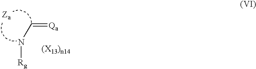


| TABLE 1 | |||||
| Elec- | |||||
| trolyte | |||||
| Sample | Elec- | Com- | Alkali Metal Salt | ||
| No. | Dye | trolyte | pound | (molar eq.*) | Remark |
| 101 | R-1 | Z-1 | (C4H9)4NI | — | comparison |
| 102 | R-1 | Z-2 | RE-1 | — | ″ |
| 103 | R-1 | Z-3 | RE-2 | — | ″ |
| 104 | R-1 | Z-4 | F-2 | — | invention |
| 105 | R-1 | Z-5 | F-4 | — | ″ |
| 106 | R-1 | Z-6 | F-4 | LiI (1.0) | ″ |
| 107 | R-1 | Z-7 | F-4 | LiN(SO2CF3)2 (1.0) | ″ |
| 108 | R-1 | Z-8 | F-6 | — | ″ |
| 109 | R-1 | Z-9 | F-6 | LiI (1.0) | ″ |
| 110 | R-1 | Z-10 | F-6 | LiN(SO2CF3)2 (1.0) | ″ |
| 111 | R-1 | Z-11 | F-7 | — | ″ |
| 112 | R-1 | Z-12 | F-7 | LiI (1.0) | ″ |
| 113 | R-1 | Z-13 | F-7 | LiN(SO2CF3)2 (1.0) | ″ |
| 114 | (1) | Z-8 | F-6 | — | ″ |
| 115 | (5) | Z-8 | F-6 | — | ″ |
| 116 | (29) | Z-8 | F-6 | — | ″ |
| 117 | (32) | Z-8 | F-6 | — | ″ |
| 118 | (37) | Z-8 | F-6 | — | ″ |
| 119 | (40) | Z-8 | F-6 | — | ″ |
| 120 | (43) | Z-8 | F-6 | — | ″ |
| 121 | R-1 | Z-14 | F-9 | — | ″ |
| 122 | R-1 | Z-15 | F-13 | — | ″ |
| 123 | R-1 | Z-16 | F-14 | — | ″ |
| 124 | R-1 | Z-17 | F-16 | — | ″ |
| 125 | R-1 | Z-18 | F-17 | — | ″ |
| 126 | R-1 | Z-19 | F-4/F-8** | — | ″ |
| 127 | R-1 | Z-20 | F-51 | — | ″ |
| 128 | R-1 | Z-21 | F-51 | LiI (1.0) | ″ |
| 129 | R-1 | Z-22 | F-51 | LIN(SO2CF3)2 | ″ |
| 130 | R-1 | Z-23 | F-54 | — | ″ |
| 131 | R-1 | Z-24 | F-54 | LiI (1.0) | ″ |
| 132 | R-1 | Z-25 | F-54 | LIN(SO2CF3)2 | ″ |
| Note: | |||||
| *Molar equivalent to the iodine salt | |||||
| **F-4/F-8 = 50/50 by mole | |||||
| TABLE 2 | |||||
| Jsc Reduction | |||||
| Sample | Jsc | Voc | after 600 hrs | ||
| No. | (mA/cm2) | (V) | FF | η (%) | (%) |
| 101 | 3.13 | 0.45 | 0.45 | 1.27 | 95 |
| 102 | 3.40 | 0.59 | 0.55 | 2.21 | 35 |
| 103 | 3.29 | 0.53 | 0.51 | 1.78 | 42 |
| 104 | 5.10 | 0.60 | 0.61 | 3.37 | 12 |
| 105 | 6.21 | 0.59 | 0.59 | 4.32 | 11 |
| 106 | 7.33 | 0.57 | 0.58 | 4.85 | 9 |
| 107 | 7.51 | 0.58 | 0.58 | 5.05 | 8 |
| 108 | 6.93 | 0.60 | 0.59 | 4.91 | 8 |
| 109 | 6.99 | 0.62 | 0.60 | 5.20 | 10 |
| 110 | 7.05 | 0.62 | 0.61 | 5.33 | 9 |
| 111 | 5.89 | 0.59 | 0.62 | 4.31 | 10 |
| 112 | 6.21 | 0.58 | 0.62 | 4.47 | 13 |
| 113 | 6.35 | 0.59 | 0.63 | 4.72 | 7 |
| 114 | 6.09 | 0.60 | 0.59 | 4.31 | 11 |
| 115 | 5.91 | 0.58 | 0.58 | 3.98 | 13 |
| 116 | 5.32 | 0.59 | 0.57 | 3.58 | 9 |
| 117 | 5.25 | 0.55 | 0.60 | 3.47 | 15 |
| 118 | 5.48 | 0.59 | 0.59 | 3.82 | 14 |
| 119 | 5.77 | 0.48 | 0.61 | 3.38 | 18 |
| 120 | 5.69 | 0.49 | 0.58 | 3.23 | 11 |
| 121 | 4.81 | 0.57 | 0.55 | 3.02 | 16 |
| 122 | 4.97 | 0.55 | 0.57 | 3.12 | 12 |
| 123 | 3.99 | 0.58 | 0.58 | 2.68 | 10 |
| 124 | 4.35 | 0.57 | 0.56 | 2.78 | 18 |
| 125 | 4.44 | 0.52 | 0.57 | 2.63 | 17 |
| 126 | 6.51 | 0.60 | 0.59 | 4.61 | 11 |
| 127 | 5.98 | 0.57 | 0.61 | 4.16 | 12 |
| 128 | 6.23 | 0.57 | 0.58 | 4.12 | 10 |
| 129 | 6.33 | 0.56 | 0.57 | 4.04 | 11 |
| 130 | 5.86 | 0.59 | 0.59 | 4.08 | 13 |
| 131 | 6.12 | 0.58 | 0.58 | 4.11 | 12 |
| 132 | 6.28 | 0.56 | 0.58 | 4.08 | 12 |
Claims (22)


Applications Claiming Priority (4)
| Application Number | Priority Date | Filing Date | Title |
|---|---|---|---|
| JP11-053162 | 1999-03-01 | ||
| JP5316299 | 1999-03-01 | ||
| JP5563699 | 1999-03-03 | ||
| JP11-055636 | 1999-03-03 |
Publications (1)
| Publication Number | Publication Date |
|---|---|
| US6495067B1 true US6495067B1 (en) | 2002-12-17 |
Family
ID=26393875
Family Applications (1)
| Application Number | Title | Priority Date | Filing Date |
|---|---|---|---|
| US09/516,628 Expired - Fee Related US6495067B1 (en) | 1999-03-01 | 2000-03-01 | Liquid crystal compound, liquid crystal mixture or composition, electrolyte comprising the same, electrochemical cell and photo-electrochemical cell containing the electrolyte |
Country Status (4)
| Country | Link |
|---|---|
| US (1) | US6495067B1 (en) |
| EP (1) | EP1033731B1 (en) |
| AT (1) | ATE332567T1 (en) |
| DE (1) | DE60029151T2 (en) |
Cited By (55)
| Publication number | Priority date | Publication date | Assignee | Title |
|---|---|---|---|---|
| US20020034690A1 (en) * | 2000-01-17 | 2002-03-21 | Michio Ono | Electrolyte composition, electrochemical cell and ionic liquid crystal monomer |
| US20030096489A1 (en) * | 1999-09-03 | 2003-05-22 | Im James S. | Methods for producing uniform large-grained and grain boundary location manipulated polycrystalline thin film semiconductors using sequential lateral solidification |
| US6627099B2 (en) * | 2000-08-22 | 2003-09-30 | Fuji Photo Film Co., Ltd. | Electrolyte composition and electrochemical battery using the same |
| US20030190530A1 (en) * | 2000-03-28 | 2003-10-09 | Li Yang | Lithium Secondary Battery |
| WO2003084688A2 (en) * | 2002-04-01 | 2003-10-16 | The Trustees Of Columbia University In The City Of New York | Method and system for providing a thin film |
| US6700058B2 (en) * | 2000-05-29 | 2004-03-02 | Sony International (Europe) Gmbh | Hole transporting agents and photoelectric conversion device comprising the same |
| US20040061843A1 (en) * | 2000-11-27 | 2004-04-01 | Im James S. | Process and mask projection system for laser crystallization processing of semiconductor film regions on a substrate |
| US20040169158A1 (en) * | 2001-03-30 | 2004-09-02 | Takashi Kato | Liquid crystalline ion conductor and method for preparation thereof |
| US20050032249A1 (en) * | 2000-03-21 | 2005-02-10 | Im James S. | Surface planarization of thin silicon films during and after processing by the sequential lateral solidification method |
| US20050034653A1 (en) * | 2001-08-27 | 2005-02-17 | James Im | Polycrystalline tft uniformity through microstructure mis-alignment |
| US20050129874A1 (en) * | 2003-12-15 | 2005-06-16 | Eastman Kodak Company | Aligned liquid crystal layer containing azolium salts and process for increasing the tilt |
| US20050150544A1 (en) * | 2003-12-05 | 2005-07-14 | Sharp Kabushiki Kaisha | Dye-sensitized solar cell |
| US20050202654A1 (en) * | 2002-08-19 | 2005-09-15 | Im James S. | Process and system for laser crystallization processing of film regions on a substrate to provide substantial uniformity, and a structure of such film regions |
| US20060030164A1 (en) * | 2002-08-19 | 2006-02-09 | Im James S | Process and system for laser crystallization processing of film regions on a substrate to minimize edge areas, and a structure of such film regions |
| US20060060130A1 (en) * | 2002-08-19 | 2006-03-23 | Im James S | Process and system for laser crystallization processing of film regions on a substrate to provide substantial uniformity within arears in such regions and edge areas thereof, and a structure of film regions |
| US20060134890A1 (en) * | 2003-02-19 | 2006-06-22 | Im James S | System and process for processing a plurality of semiconductor thin films which are crystallized using sequential lateral solidification techniques |
| US20060188662A1 (en) * | 2003-01-24 | 2006-08-24 | Farrand Louise D | Ionic mesogenic compounds |
| US7115503B2 (en) | 2000-10-10 | 2006-10-03 | The Trustees Of Columbia University In The City Of New York | Method and apparatus for processing thin metal layers |
| WO2006126861A1 (en) * | 2005-05-27 | 2006-11-30 | Busan National University Industry-University Cooperation Foundation | Solid-state electrolyte composition containing liquid crystal materials and dye-sensitized solar cells using thereof |
| US7164152B2 (en) | 2003-09-16 | 2007-01-16 | The Trustees Of Columbia University In The City Of New York | Laser-irradiated thin films having variable thickness |
| US20070032096A1 (en) * | 2003-09-16 | 2007-02-08 | Im James S | System and process for providing multiple beam sequential lateral solidification |
| CN100356587C (en) * | 2004-03-23 | 2007-12-19 | 中国科学院等离子体物理研究所 | Large area internal series dye sensitization nano-thin film solar cell and producing method thereof |
| CN100356586C (en) * | 2004-03-23 | 2007-12-19 | 中国科学院等离子体物理研究所 | Large area internal series dye sensitization nano thin film solar cell and producing method thereof |
| US7311778B2 (en) | 2003-09-19 | 2007-12-25 | The Trustees Of Columbia University In The City Of New York | Single scan irradiation for crystallization of thin films |
| US7318866B2 (en) | 2003-09-16 | 2008-01-15 | The Trustees Of Columbia University In The City Of New York | Systems and methods for inducing crystallization of thin films using multiple optical paths |
| US7364952B2 (en) | 2003-09-16 | 2008-04-29 | The Trustees Of Columbia University In The City Of New York | Systems and methods for processing thin films |
| US7414188B2 (en) * | 2002-01-25 | 2008-08-19 | Konarka Technologies, Inc. | Co-sensitizers for dye sensitized solar cells |
| US20080236666A1 (en) * | 2006-07-27 | 2008-10-02 | Commissariat A L'energie Atomique | Polymerizable diazonium salts, process for the preparation thereof and uses thereof |
| US7645337B2 (en) | 2004-11-18 | 2010-01-12 | The Trustees Of Columbia University In The City Of New York | Systems and methods for creating crystallographic-orientation controlled poly-silicon films |
| US7718517B2 (en) | 2002-08-19 | 2010-05-18 | Im James S | Single-shot semiconductor processing system and method having various irradiation patterns |
| US7759230B2 (en) | 2003-09-16 | 2010-07-20 | The Trustees Of Columbia University In The City Of New York | System for providing a continuous motion sequential lateral solidification for reducing or eliminating artifacts in overlap regions, and a mask for facilitating such artifact reduction/elimination |
| US20100228035A1 (en) * | 2002-04-05 | 2010-09-09 | University Of South Alabama | Functionalized Ionic Liquids, and Methods of Use Thereof |
| US20110151317A1 (en) * | 2008-07-11 | 2011-06-23 | Commissariat A L'energie Atomique Et Aux Energies Alternatives | Ionic liquid electrolytes comprising an anionic surfactant and electrochemical devices such as accumulators comprising them |
| US20110203644A1 (en) * | 2010-02-22 | 2011-08-25 | Brite Hellas Ae | Quasi-solid-state photoelectrochemical solar cell formed using inkjet printing and nanocomposite organic-inorganic material |
| US8012861B2 (en) | 2007-11-21 | 2011-09-06 | The Trustees Of Columbia University In The City Of New York | Systems and methods for preparing epitaxially textured polycrystalline films |
| US8063338B2 (en) | 2003-09-16 | 2011-11-22 | The Trustees Of Columbia In The City Of New York | Enhancing the width of polycrystalline grains with mask |
| US8221544B2 (en) | 2005-04-06 | 2012-07-17 | The Trustees Of Columbia University In The City Of New York | Line scan sequential lateral solidification of thin films |
| US8415670B2 (en) | 2007-09-25 | 2013-04-09 | The Trustees Of Columbia University In The City Of New York | Methods of producing high uniformity in thin film transistor devices fabricated on laterally crystallized thin films |
| US8426296B2 (en) | 2007-11-21 | 2013-04-23 | The Trustees Of Columbia University In The City Of New York | Systems and methods for preparing epitaxially textured polycrystalline films |
| US8440581B2 (en) | 2009-11-24 | 2013-05-14 | The Trustees Of Columbia University In The City Of New York | Systems and methods for non-periodic pulse sequential lateral solidification |
| US8557040B2 (en) | 2007-11-21 | 2013-10-15 | The Trustees Of Columbia University In The City Of New York | Systems and methods for preparation of epitaxially textured thick films |
| US20130280555A1 (en) * | 2012-04-20 | 2013-10-24 | Samsung Electro-Mechanics Japan Advanced Technology Co., Ltd. | Magnetic disk, lubricant-layer-forming composition for forming a lubricant layer, and method for forming the lubricant layer |
| US8569155B2 (en) | 2008-02-29 | 2013-10-29 | The Trustees Of Columbia University In The City Of New York | Flash lamp annealing crystallization for large area thin films |
| US8598588B2 (en) | 2005-12-05 | 2013-12-03 | The Trustees Of Columbia University In The City Of New York | Systems and methods for processing a film, and thin films |
| US8614471B2 (en) | 2007-09-21 | 2013-12-24 | The Trustees Of Columbia University In The City Of New York | Collections of laterally crystallized semiconductor islands for use in thin film transistors |
| US8663387B2 (en) | 2003-09-16 | 2014-03-04 | The Trustees Of Columbia University In The City Of New York | Method and system for facilitating bi-directional growth |
| US20140212080A1 (en) * | 2013-01-25 | 2014-07-31 | Samsung Electro-Mechanics Japan Advanced Technolog Co., Ltd. | Component for use in a bearing device and a method for forming a lubricant layer |
| US8796159B2 (en) | 2003-09-16 | 2014-08-05 | The Trustees Of Columbia University In The City Of New York | Processes and systems for laser crystallization processing of film regions on a substrate utilizing a line-type beam, and structures of such film regions |
| US8802580B2 (en) | 2008-11-14 | 2014-08-12 | The Trustees Of Columbia University In The City Of New York | Systems and methods for the crystallization of thin films |
| US9087696B2 (en) | 2009-11-03 | 2015-07-21 | The Trustees Of Columbia University In The City Of New York | Systems and methods for non-periodic pulse partial melt film processing |
| US20160109356A1 (en) * | 2013-06-04 | 2016-04-21 | Ushio Denki Kabushiki Kaisha | Microchip and film forming method for metal thin film of microchip |
| US20160115389A1 (en) * | 2013-07-12 | 2016-04-28 | Lg Chem, Ltd. | Liquid crystal cell |
| US9646831B2 (en) | 2009-11-03 | 2017-05-09 | The Trustees Of Columbia University In The City Of New York | Advanced excimer laser annealing for thin films |
| CN107636830A (en) * | 2015-06-05 | 2018-01-26 | 索尼半导体解决方案公司 | Solid-state imaging element, photoelectric conversion film, electronic barrier layer, camera device and electronic equipment |
| US10944132B2 (en) * | 2015-02-18 | 2021-03-09 | Microsoft Technology Licensing, Llc | Dynamically changing internal state of a battery |
Families Citing this family (4)
| Publication number | Priority date | Publication date | Assignee | Title |
|---|---|---|---|---|
| JP4278080B2 (en) | 2000-09-27 | 2009-06-10 | 富士フイルム株式会社 | High sensitivity light receiving element and image sensor |
| JP2003100357A (en) * | 2001-09-20 | 2003-04-04 | Fuji Photo Film Co Ltd | Manufacturing method of photoelectric conversion element, photoelectric conversion element, and photoelectric cell |
| US8168830B2 (en) | 2004-07-23 | 2012-05-01 | Sigma-Aldrich Co. Llc | High stability diionic liquid salts |
| KR102163732B1 (en) * | 2013-10-10 | 2020-10-12 | 삼성전자주식회사 | Lithium air battery |
Citations (8)
| Publication number | Priority date | Publication date | Assignee | Title |
|---|---|---|---|---|
| US4801713A (en) * | 1987-01-27 | 1989-01-31 | Nippon Gohsei Kagaku Kogyo Kabushiki Kaisha | Organic complexes of a cation of a heterocyclic nitrogen compound and an anion of a 2,5-disubstituted-7,7,8,8-tetracyanoquinodiethmane |
| US5084365A (en) * | 1988-02-12 | 1992-01-28 | Michael Gratzel | Photo-electrochemical cell and process of making same |
| US5091274A (en) * | 1990-05-02 | 1992-02-25 | National Science Council | Ionic conducting polymer electrolytes based on a side-chain crystalline polymer |
| JPH1053585A (en) * | 1996-04-19 | 1998-02-24 | Nippon Chem Ind Co Ltd | Pyridinium type inonic compound derivative, its production and liquid crystal substance |
| US6096392A (en) * | 1997-07-09 | 2000-08-01 | Daicel Chemical Industries, Ltd. | Cholesteric liquid crystal display element |
| US6171522B1 (en) * | 1996-12-30 | 2001-01-09 | Hydro-Qu{acute over (e)}bec | Heterocyclic aromatic anion salts, and their uses as ionic conducting materials |
| US6376765B1 (en) * | 1999-08-04 | 2002-04-23 | Fuji Photo Film Co., Ltd. | Electrolyte composition, photoelectric conversion device and photo-electrochemical cell |
| US6384321B1 (en) * | 1999-09-24 | 2002-05-07 | Kabushiki Kaisha Toshiba | Electrolyte composition, photosensitized solar cell using said electrolyte composition, and method of manufacturing photosensitized solar cell |
Family Cites Families (2)
| Publication number | Priority date | Publication date | Assignee | Title |
|---|---|---|---|---|
| US4414080A (en) * | 1982-05-10 | 1983-11-08 | The United States Of America As Represented By The Administrator Of The National Aeronautics And Space Administration | Photoelectrochemical electrodes |
| DE4445584A1 (en) * | 1994-12-20 | 1996-06-27 | Basf Ag | Use of organic materials of high nonionic charge carrier mobility |
-
2000
- 2000-02-23 EP EP00103822A patent/EP1033731B1/en not_active Expired - Lifetime
- 2000-02-23 DE DE60029151T patent/DE60029151T2/en not_active Expired - Lifetime
- 2000-02-23 AT AT00103822T patent/ATE332567T1/en not_active IP Right Cessation
- 2000-03-01 US US09/516,628 patent/US6495067B1/en not_active Expired - Fee Related
Patent Citations (8)
| Publication number | Priority date | Publication date | Assignee | Title |
|---|---|---|---|---|
| US4801713A (en) * | 1987-01-27 | 1989-01-31 | Nippon Gohsei Kagaku Kogyo Kabushiki Kaisha | Organic complexes of a cation of a heterocyclic nitrogen compound and an anion of a 2,5-disubstituted-7,7,8,8-tetracyanoquinodiethmane |
| US5084365A (en) * | 1988-02-12 | 1992-01-28 | Michael Gratzel | Photo-electrochemical cell and process of making same |
| US5091274A (en) * | 1990-05-02 | 1992-02-25 | National Science Council | Ionic conducting polymer electrolytes based on a side-chain crystalline polymer |
| JPH1053585A (en) * | 1996-04-19 | 1998-02-24 | Nippon Chem Ind Co Ltd | Pyridinium type inonic compound derivative, its production and liquid crystal substance |
| US6171522B1 (en) * | 1996-12-30 | 2001-01-09 | Hydro-Qu{acute over (e)}bec | Heterocyclic aromatic anion salts, and their uses as ionic conducting materials |
| US6096392A (en) * | 1997-07-09 | 2000-08-01 | Daicel Chemical Industries, Ltd. | Cholesteric liquid crystal display element |
| US6376765B1 (en) * | 1999-08-04 | 2002-04-23 | Fuji Photo Film Co., Ltd. | Electrolyte composition, photoelectric conversion device and photo-electrochemical cell |
| US6384321B1 (en) * | 1999-09-24 | 2002-05-07 | Kabushiki Kaisha Toshiba | Electrolyte composition, photosensitized solar cell using said electrolyte composition, and method of manufacturing photosensitized solar cell |
Non-Patent Citations (4)
| Title |
|---|
| Caplus 1980:503744.* * |
| Japanese Patent Application No. Hei. 9-113570 (filed Apr. 16, 1997), JP-A-1053585 (published Feb. 24, 1998). |
| STN International, American Chemical Society, 1999, RN 150697-81-7, p. 12. |
| STN International, American Chemical Society, 1999, RN 72668-04-3, p. 303. |
Cited By (105)
| Publication number | Priority date | Publication date | Assignee | Title |
|---|---|---|---|---|
| US7319056B2 (en) | 1996-05-28 | 2008-01-15 | The Trustees Of Columbia University In The City Of New York | Methods for producing uniform large-grained and grain boundary location manipulated polycrystalline thin film semiconductors using sequential lateral solidification |
| US20050255640A1 (en) * | 1996-05-28 | 2005-11-17 | Im James S | Methods for producing uniform large-grained and grain boundary location manipulated polycrystalline thin film semiconductors using sequential lateral solidification |
| US8859436B2 (en) | 1996-05-28 | 2014-10-14 | The Trustees Of Columbia University In The City Of New York | Uniform large-grained and grain boundary location manipulated polycrystalline thin film semiconductors formed using sequential lateral solidification and devices formed thereon |
| US8680427B2 (en) | 1996-05-28 | 2014-03-25 | The Trustees Of Columbia University In The City Of New York | Uniform large-grained and gain boundary location manipulated polycrystalline thin film semiconductors formed using sequential lateral solidification and devices formed thereon |
| US8278659B2 (en) | 1996-05-28 | 2012-10-02 | The Trustees Of Columbia University In The City Of New York | Uniform large-grained and grain boundary location manipulated polycrystalline thin film semiconductors formed using sequential lateral solidification and devices formed thereon |
| US7679028B2 (en) | 1996-05-28 | 2010-03-16 | The Trustees Of Columbia University In The City Of New York | Methods for producing uniform large-grained and grain boundary location manipulated polycrystalline thin film semiconductors using sequential lateral solidification |
| US20030096489A1 (en) * | 1999-09-03 | 2003-05-22 | Im James S. | Methods for producing uniform large-grained and grain boundary location manipulated polycrystalline thin film semiconductors using sequential lateral solidification |
| US7029996B2 (en) | 1999-09-03 | 2006-04-18 | The Trustees Of Columbia University In The City Of New York | Methods for producing uniform large-grained and grain boundary location manipulated polycrystalline thin film semiconductors using sequential lateral solidification |
| US20020034690A1 (en) * | 2000-01-17 | 2002-03-21 | Michio Ono | Electrolyte composition, electrochemical cell and ionic liquid crystal monomer |
| US6727023B2 (en) * | 2000-01-17 | 2004-04-27 | Fuji Photo Film Co., Ltd. | Electrolyte composition, electrochemical cell and ionic liquid crystal monomer |
| US7220660B2 (en) | 2000-03-21 | 2007-05-22 | The Trustees Of Columbia University In The City Of New York | Surface planarization of thin silicon films during and after processing by the sequential lateral solidification method |
| US20050032249A1 (en) * | 2000-03-21 | 2005-02-10 | Im James S. | Surface planarization of thin silicon films during and after processing by the sequential lateral solidification method |
| US7704862B2 (en) | 2000-03-21 | 2010-04-27 | The Trustees Of Columbia University | Surface planarization of thin silicon films during and after processing by the sequential lateral solidification method |
| US20030190530A1 (en) * | 2000-03-28 | 2003-10-09 | Li Yang | Lithium Secondary Battery |
| US20040177879A1 (en) * | 2000-05-29 | 2004-09-16 | Gabriele Nelles | Hole transporting agents and photoelectric conversion device comprising the same |
| US7132598B2 (en) * | 2000-05-29 | 2006-11-07 | Sony Deutschland Gmbh | Hole transporting agents and photoelectric conversion device comprising the same |
| US6700058B2 (en) * | 2000-05-29 | 2004-03-02 | Sony International (Europe) Gmbh | Hole transporting agents and photoelectric conversion device comprising the same |
| US6627099B2 (en) * | 2000-08-22 | 2003-09-30 | Fuji Photo Film Co., Ltd. | Electrolyte composition and electrochemical battery using the same |
| US7709378B2 (en) | 2000-10-10 | 2010-05-04 | The Trustees Of Columbia University In The City Of New York | Method and apparatus for processing thin metal layers |
| US7115503B2 (en) | 2000-10-10 | 2006-10-03 | The Trustees Of Columbia University In The City Of New York | Method and apparatus for processing thin metal layers |
| US6961117B2 (en) | 2000-11-27 | 2005-11-01 | The Trustees Of Columbia University In The City Of New York | Process and mask projection system for laser crystallization processing of semiconductor film regions on a substrate |
| US20040061843A1 (en) * | 2000-11-27 | 2004-04-01 | Im James S. | Process and mask projection system for laser crystallization processing of semiconductor film regions on a substrate |
| US20060011887A1 (en) * | 2001-03-30 | 2006-01-19 | Takashi Kato | Liquid-crystalline ionic conductor and method for producing the same |
| US7166238B2 (en) | 2001-03-30 | 2007-01-23 | Japan Science And Technology Corporation | Liquid-crystalline ionic conductor and method for producing the same |
| US20040169158A1 (en) * | 2001-03-30 | 2004-09-02 | Takashi Kato | Liquid crystalline ion conductor and method for preparation thereof |
| US20050034653A1 (en) * | 2001-08-27 | 2005-02-17 | James Im | Polycrystalline tft uniformity through microstructure mis-alignment |
| US7160763B2 (en) | 2001-08-27 | 2007-01-09 | The Trustees Of Columbia University In The City Of New York | Polycrystalline TFT uniformity through microstructure mis-alignment |
| US7414188B2 (en) * | 2002-01-25 | 2008-08-19 | Konarka Technologies, Inc. | Co-sensitizers for dye sensitized solar cells |
| WO2003084688A3 (en) * | 2002-04-01 | 2004-07-15 | Univ Columbia | Method and system for providing a thin film |
| US20060006464A1 (en) * | 2002-04-01 | 2006-01-12 | Im James S | Method and system for providing a thin film with a controlled crystal orientation using pulsed laser induced melting and nucleation-initiated crystallization |
| US7399359B2 (en) | 2002-04-01 | 2008-07-15 | The Trustees of Columbia University in theCity of New York | Method and system for providing a thin film with a controlled crystal orientation using pulsed laser induced melting and nucleation-initiated crystallization |
| WO2003084688A2 (en) * | 2002-04-01 | 2003-10-16 | The Trustees Of Columbia University In The City Of New York | Method and system for providing a thin film |
| US20100228035A1 (en) * | 2002-04-05 | 2010-09-09 | University Of South Alabama | Functionalized Ionic Liquids, and Methods of Use Thereof |
| US8674135B2 (en) * | 2002-04-05 | 2014-03-18 | University Of South Alabama | Functionalized ionic liquids, and methods of use thereof |
| US7718517B2 (en) | 2002-08-19 | 2010-05-18 | Im James S | Single-shot semiconductor processing system and method having various irradiation patterns |
| US20060060130A1 (en) * | 2002-08-19 | 2006-03-23 | Im James S | Process and system for laser crystallization processing of film regions on a substrate to provide substantial uniformity within arears in such regions and edge areas thereof, and a structure of film regions |
| US8411713B2 (en) | 2002-08-19 | 2013-04-02 | The Trustees Of Columbia University In The City Of New York | Process and system for laser crystallization processing of film regions on a substrate to minimize edge areas, and structure of such film regions |
| US20060030164A1 (en) * | 2002-08-19 | 2006-02-09 | Im James S | Process and system for laser crystallization processing of film regions on a substrate to minimize edge areas, and a structure of such film regions |
| US8479681B2 (en) | 2002-08-19 | 2013-07-09 | The Trustees Of Columbia University In The City Of New York | Single-shot semiconductor processing system and method having various irradiation patterns |
| US7259081B2 (en) | 2002-08-19 | 2007-08-21 | Im James S | Process and system for laser crystallization processing of film regions on a substrate to provide substantial uniformity, and a structure of such film regions |
| US20050202654A1 (en) * | 2002-08-19 | 2005-09-15 | Im James S. | Process and system for laser crystallization processing of film regions on a substrate to provide substantial uniformity, and a structure of such film regions |
| US8883656B2 (en) | 2002-08-19 | 2014-11-11 | The Trustees Of Columbia University In The City Of New York | Single-shot semiconductor processing system and method having various irradiation patterns |
| US7906414B2 (en) | 2002-08-19 | 2011-03-15 | The Trustees Of Columbia University In The City Of New York | Single-shot semiconductor processing system and method having various irradiation patterns |
| US7300858B2 (en) | 2002-08-19 | 2007-11-27 | The Trustees Of Columbia University In The City Of New York | Laser crystallization and selective patterning using multiple beamlets |
| US20060188662A1 (en) * | 2003-01-24 | 2006-08-24 | Farrand Louise D | Ionic mesogenic compounds |
| US7902052B2 (en) | 2003-02-19 | 2011-03-08 | The Trustees Of Columbia University In The City Of New York | System and process for processing a plurality of semiconductor thin films which are crystallized using sequential lateral solidification techniques |
| US7341928B2 (en) | 2003-02-19 | 2008-03-11 | The Trustees Of Columbia University In The City Of New York | System and process for processing a plurality of semiconductor thin films which are crystallized using sequential lateral solidification techniques |
| US20060134890A1 (en) * | 2003-02-19 | 2006-06-22 | Im James S | System and process for processing a plurality of semiconductor thin films which are crystallized using sequential lateral solidification techniques |
| US20070032096A1 (en) * | 2003-09-16 | 2007-02-08 | Im James S | System and process for providing multiple beam sequential lateral solidification |
| US8063338B2 (en) | 2003-09-16 | 2011-11-22 | The Trustees Of Columbia In The City Of New York | Enhancing the width of polycrystalline grains with mask |
| US8476144B2 (en) | 2003-09-16 | 2013-07-02 | The Trustees Of Columbia University In The City Of New York | Method for providing a continuous motion sequential lateral solidification for reducing or eliminating artifacts in edge regions, and a mask for facilitating such artifact reduction/elimination |
| US8796159B2 (en) | 2003-09-16 | 2014-08-05 | The Trustees Of Columbia University In The City Of New York | Processes and systems for laser crystallization processing of film regions on a substrate utilizing a line-type beam, and structures of such film regions |
| US7691687B2 (en) | 2003-09-16 | 2010-04-06 | The Trustees Of Columbia University In The City Of New York | Method for processing laser-irradiated thin films having variable thickness |
| US7759230B2 (en) | 2003-09-16 | 2010-07-20 | The Trustees Of Columbia University In The City Of New York | System for providing a continuous motion sequential lateral solidification for reducing or eliminating artifacts in overlap regions, and a mask for facilitating such artifact reduction/elimination |
| US9466402B2 (en) | 2003-09-16 | 2016-10-11 | The Trustees Of Columbia University In The City Of New York | Processes and systems for laser crystallization processing of film regions on a substrate utilizing a line-type beam, and structures of such film regions |
| US7164152B2 (en) | 2003-09-16 | 2007-01-16 | The Trustees Of Columbia University In The City Of New York | Laser-irradiated thin films having variable thickness |
| US8715412B2 (en) | 2003-09-16 | 2014-05-06 | The Trustees Of Columbia University In The City Of New York | Laser-irradiated thin films having variable thickness |
| US8034698B2 (en) | 2003-09-16 | 2011-10-11 | The Trustees Of Columbia University In The City Of New York | Systems and methods for inducing crystallization of thin films using multiple optical paths |
| US7364952B2 (en) | 2003-09-16 | 2008-04-29 | The Trustees Of Columbia University In The City Of New York | Systems and methods for processing thin films |
| US8663387B2 (en) | 2003-09-16 | 2014-03-04 | The Trustees Of Columbia University In The City Of New York | Method and system for facilitating bi-directional growth |
| US7318866B2 (en) | 2003-09-16 | 2008-01-15 | The Trustees Of Columbia University In The City Of New York | Systems and methods for inducing crystallization of thin films using multiple optical paths |
| US7964480B2 (en) | 2003-09-19 | 2011-06-21 | Trustees Of Columbia University In The City Of New York | Single scan irradiation for crystallization of thin films |
| US8445365B2 (en) | 2003-09-19 | 2013-05-21 | The Trustees Of Columbia University In The City Of New York | Single scan irradiation for crystallization of thin films |
| US7311778B2 (en) | 2003-09-19 | 2007-12-25 | The Trustees Of Columbia University In The City Of New York | Single scan irradiation for crystallization of thin films |
| US20050150544A1 (en) * | 2003-12-05 | 2005-07-14 | Sharp Kabushiki Kaisha | Dye-sensitized solar cell |
| US20050129874A1 (en) * | 2003-12-15 | 2005-06-16 | Eastman Kodak Company | Aligned liquid crystal layer containing azolium salts and process for increasing the tilt |
| US7097888B2 (en) * | 2003-12-15 | 2006-08-29 | Eastman Kodak Company | Aligned liquid crystal layer containing azolium salts and process for increasing the tilt |
| CN100356586C (en) * | 2004-03-23 | 2007-12-19 | 中国科学院等离子体物理研究所 | Large area internal series dye sensitization nano thin film solar cell and producing method thereof |
| CN100356587C (en) * | 2004-03-23 | 2007-12-19 | 中国科学院等离子体物理研究所 | Large area internal series dye sensitization nano-thin film solar cell and producing method thereof |
| US8734584B2 (en) | 2004-11-18 | 2014-05-27 | The Trustees Of Columbia University In The City Of New York | Systems and methods for creating crystallographic-orientation controlled poly-silicon films |
| US7645337B2 (en) | 2004-11-18 | 2010-01-12 | The Trustees Of Columbia University In The City Of New York | Systems and methods for creating crystallographic-orientation controlled poly-silicon films |
| US8221544B2 (en) | 2005-04-06 | 2012-07-17 | The Trustees Of Columbia University In The City Of New York | Line scan sequential lateral solidification of thin films |
| US8617313B2 (en) | 2005-04-06 | 2013-12-31 | The Trustees Of Columbia University In The City Of New York | Line scan sequential lateral solidification of thin films |
| WO2006126861A1 (en) * | 2005-05-27 | 2006-11-30 | Busan National University Industry-University Cooperation Foundation | Solid-state electrolyte composition containing liquid crystal materials and dye-sensitized solar cells using thereof |
| US20090133746A1 (en) * | 2005-05-27 | 2009-05-28 | Sung Ho Jin | Solid-State Electrolyte Composition Containing Liquid Crystal Materials and Dye-Sensitized Solar Cells Using the Same |
| US8598588B2 (en) | 2005-12-05 | 2013-12-03 | The Trustees Of Columbia University In The City Of New York | Systems and methods for processing a film, and thin films |
| US20100184932A1 (en) * | 2006-07-27 | 2010-07-22 | Commissariat A L'energie Atomique | Polymerizable Diazonium Salts, Process For The Preparation Thereof And Uses Thereof |
| US7812139B2 (en) * | 2006-07-27 | 2010-10-12 | Commissariat A L'energie Atomique | Polymerizable diazonium salts, process for the preparation thereof and uses thereof |
| US20080236666A1 (en) * | 2006-07-27 | 2008-10-02 | Commissariat A L'energie Atomique | Polymerizable diazonium salts, process for the preparation thereof and uses thereof |
| US8389696B2 (en) | 2006-07-27 | 2013-03-05 | Commissariat A L'energie Atomique | Polymerizable diazonium salts, process for the preparation thereof and uses thereof |
| US8614471B2 (en) | 2007-09-21 | 2013-12-24 | The Trustees Of Columbia University In The City Of New York | Collections of laterally crystallized semiconductor islands for use in thin film transistors |
| US9012309B2 (en) | 2007-09-21 | 2015-04-21 | The Trustees Of Columbia University In The City Of New York | Collections of laterally crystallized semiconductor islands for use in thin film transistors |
| US8415670B2 (en) | 2007-09-25 | 2013-04-09 | The Trustees Of Columbia University In The City Of New York | Methods of producing high uniformity in thin film transistor devices fabricated on laterally crystallized thin films |
| US8557040B2 (en) | 2007-11-21 | 2013-10-15 | The Trustees Of Columbia University In The City Of New York | Systems and methods for preparation of epitaxially textured thick films |
| US8426296B2 (en) | 2007-11-21 | 2013-04-23 | The Trustees Of Columbia University In The City Of New York | Systems and methods for preparing epitaxially textured polycrystalline films |
| US8012861B2 (en) | 2007-11-21 | 2011-09-06 | The Trustees Of Columbia University In The City Of New York | Systems and methods for preparing epitaxially textured polycrystalline films |
| US8871022B2 (en) | 2007-11-21 | 2014-10-28 | The Trustees Of Columbia University In The City Of New York | Systems and methods for preparation of epitaxially textured thick films |
| US8569155B2 (en) | 2008-02-29 | 2013-10-29 | The Trustees Of Columbia University In The City Of New York | Flash lamp annealing crystallization for large area thin films |
| US20110151317A1 (en) * | 2008-07-11 | 2011-06-23 | Commissariat A L'energie Atomique Et Aux Energies Alternatives | Ionic liquid electrolytes comprising an anionic surfactant and electrochemical devices such as accumulators comprising them |
| US9123972B2 (en) * | 2008-07-11 | 2015-09-01 | Commissariat A L'energie Atomique Et Aux Energies Alternatives | Ionic liquid electrolytes comprising an anionic surfactant and electrochemical devices such as accumulators comprising them |
| US8802580B2 (en) | 2008-11-14 | 2014-08-12 | The Trustees Of Columbia University In The City Of New York | Systems and methods for the crystallization of thin films |
| US9087696B2 (en) | 2009-11-03 | 2015-07-21 | The Trustees Of Columbia University In The City Of New York | Systems and methods for non-periodic pulse partial melt film processing |
| US9646831B2 (en) | 2009-11-03 | 2017-05-09 | The Trustees Of Columbia University In The City Of New York | Advanced excimer laser annealing for thin films |
| US8440581B2 (en) | 2009-11-24 | 2013-05-14 | The Trustees Of Columbia University In The City Of New York | Systems and methods for non-periodic pulse sequential lateral solidification |
| US8889569B2 (en) | 2009-11-24 | 2014-11-18 | The Trustees Of Columbia University In The City Of New York | Systems and methods for non-periodic pulse sequential lateral soldification |
| US20110203644A1 (en) * | 2010-02-22 | 2011-08-25 | Brite Hellas Ae | Quasi-solid-state photoelectrochemical solar cell formed using inkjet printing and nanocomposite organic-inorganic material |
| US20130280555A1 (en) * | 2012-04-20 | 2013-10-24 | Samsung Electro-Mechanics Japan Advanced Technology Co., Ltd. | Magnetic disk, lubricant-layer-forming composition for forming a lubricant layer, and method for forming the lubricant layer |
| US20140212080A1 (en) * | 2013-01-25 | 2014-07-31 | Samsung Electro-Mechanics Japan Advanced Technolog Co., Ltd. | Component for use in a bearing device and a method for forming a lubricant layer |
| US20160109356A1 (en) * | 2013-06-04 | 2016-04-21 | Ushio Denki Kabushiki Kaisha | Microchip and film forming method for metal thin film of microchip |
| US9696253B2 (en) * | 2013-06-04 | 2017-07-04 | Ushio Denki Kabushiki Kaisha | Microchip and film forming method for metal thin film of microchip |
| US10261007B2 (en) | 2013-06-04 | 2019-04-16 | Ushio Denki Kabushiki Kaisha | Microchip |
| US20160115389A1 (en) * | 2013-07-12 | 2016-04-28 | Lg Chem, Ltd. | Liquid crystal cell |
| US9758726B2 (en) * | 2013-07-12 | 2017-09-12 | Lg Chem, Ltd. | Liquid crystal cell |
| US10944132B2 (en) * | 2015-02-18 | 2021-03-09 | Microsoft Technology Licensing, Llc | Dynamically changing internal state of a battery |
| CN107636830A (en) * | 2015-06-05 | 2018-01-26 | 索尼半导体解决方案公司 | Solid-state imaging element, photoelectric conversion film, electronic barrier layer, camera device and electronic equipment |
Also Published As
| Publication number | Publication date |
|---|---|
| ATE332567T1 (en) | 2006-07-15 |
| DE60029151T2 (en) | 2007-05-31 |
| EP1033731B1 (en) | 2006-07-05 |
| DE60029151D1 (en) | 2006-08-17 |
| EP1033731A3 (en) | 2004-02-25 |
| EP1033731A2 (en) | 2000-09-06 |
Similar Documents
| Publication | Publication Date | Title |
|---|---|---|
| US6495067B1 (en) | Liquid crystal compound, liquid crystal mixture or composition, electrolyte comprising the same, electrochemical cell and photo-electrochemical cell containing the electrolyte | |
| JP5022413B2 (en) | Imidazolium compounds and pyridinium compounds | |
| US6291763B1 (en) | Photoelectric conversion device and photo cell | |
| EP0986079B1 (en) | Photo-electrochemical cell | |
| EP1083582B1 (en) | Dye sensitized photoelectrochemical cell | |
| US20020015881A1 (en) | Photoelectric conversion device and photo cell | |
| JP4443713B2 (en) | Semiconductor fine particles, photoelectric conversion element and photovoltaic cell | |
| JP4360575B2 (en) | Liquid crystal compound, liquid crystal mixture, liquid crystal composition, electrolyte, electrochemical cell and photoelectrochemical cell | |
| JP4620224B2 (en) | Electrolyte composition | |
| JP4638973B2 (en) | Photoelectric conversion element and photovoltaic cell | |
| JP2000323190A (en) | Electrolyte composition, photoelectric transfer element and photo-electrochemical battery | |
| JP4500420B2 (en) | Photoelectric conversion element and photovoltaic cell | |
| JP2001319698A (en) | Photoelectric conversion element and photoelectric cell | |
| JP4111360B2 (en) | Gel electrolyte, gel electrolyte for photoelectrochemical cell, and photoelectrochemical cell | |
| JP4392773B2 (en) | Photoelectric conversion element and photoelectrochemical cell | |
| JP2001167630A (en) | Electrolyte composition, photoelectric transducer and photoelectrochemical cell | |
| JP4970641B2 (en) | Photoelectric conversion element and photovoltaic cell using the same | |
| JP2001167808A (en) | Photoelectric conversion element and photocell | |
| EP0980082B1 (en) | Photo-electrochemical cell using an organic electrolyte | |
| JP4460686B2 (en) | Photoelectric conversion element and photoelectrochemical cell | |
| JP4217320B2 (en) | Photoelectric conversion element and photoelectrochemical cell | |
| JP2001283943A (en) | Photoelectric transfer element and photoelectrochemical cell | |
| JP2001035253A (en) | Electrolyte composition, photoelectric transfer element and photo-electrochemical battery | |
| JP2003100357A (en) | Manufacturing method of photoelectric conversion element, photoelectric conversion element, and photoelectric cell | |
| JP2000036608A (en) | Gel electrolyte, photoelectric transducer and optical regenerative photoelectric chemical cell |
Legal Events
| Date | Code | Title | Description |
|---|---|---|---|
| AS | Assignment |
Owner name: FUJI PHOTO FILM CO. LTD., JAPAN Free format text: ASSIGNMENT OF ASSIGNORS INTEREST;ASSIGNOR:ONO, MICHIO;REEL/FRAME:010599/0916 Effective date: 20000216 |
|
| FEPP | Fee payment procedure |
Free format text: PAYOR NUMBER ASSIGNED (ORIGINAL EVENT CODE: ASPN); ENTITY STATUS OF PATENT OWNER: LARGE ENTITY |
|
| FPAY | Fee payment |
Year of fee payment: 4 |
|
| AS | Assignment |
Owner name: FUJIFILM HOLDINGS CORPORATION, JAPAN Free format text: CHANGE OF NAME;ASSIGNOR:FUJI PHOTO FILM CO., LTD.;REEL/FRAME:018898/0872 Effective date: 20061001 Owner name: FUJIFILM HOLDINGS CORPORATION,JAPAN Free format text: CHANGE OF NAME;ASSIGNOR:FUJI PHOTO FILM CO., LTD.;REEL/FRAME:018898/0872 Effective date: 20061001 |
|
| AS | Assignment |
Owner name: FUJIFILM CORPORATION, JAPAN Free format text: ASSIGNMENT OF ASSIGNORS INTEREST;ASSIGNOR:FUJIFILM HOLDINGS CORPORATION;REEL/FRAME:018934/0001 Effective date: 20070130 Owner name: FUJIFILM CORPORATION,JAPAN Free format text: ASSIGNMENT OF ASSIGNORS INTEREST;ASSIGNOR:FUJIFILM HOLDINGS CORPORATION;REEL/FRAME:018934/0001 Effective date: 20070130 |
|
| FPAY | Fee payment |
Year of fee payment: 8 |
|
| REMI | Maintenance fee reminder mailed | ||
| LAPS | Lapse for failure to pay maintenance fees | ||
| STCH | Information on status: patent discontinuation |
Free format text: PATENT EXPIRED DUE TO NONPAYMENT OF MAINTENANCE FEES UNDER 37 CFR 1.362 |
|
| FP | Lapsed due to failure to pay maintenance fee |
Effective date: 20141217 |