US6498592B1 - Display tile structure using organic light emitting materials - Google Patents
Display tile structure using organic light emitting materials Download PDFInfo
- Publication number
- US6498592B1 US6498592B1 US09/709,904 US70990400A US6498592B1 US 6498592 B1 US6498592 B1 US 6498592B1 US 70990400 A US70990400 A US 70990400A US 6498592 B1 US6498592 B1 US 6498592B1
- Authority
- US
- United States
- Prior art keywords
- pixel
- substrate
- display
- coupled
- tile
- Prior art date
- Legal status (The legal status is an assumption and is not a legal conclusion. Google has not performed a legal analysis and makes no representation as to the accuracy of the status listed.)
- Expired - Lifetime, expires
Links
Images


Classifications
-
- G—PHYSICS
- G02—OPTICS
- G02F—OPTICAL DEVICES OR ARRANGEMENTS FOR THE CONTROL OF LIGHT BY MODIFICATION OF THE OPTICAL PROPERTIES OF THE MEDIA OF THE ELEMENTS INVOLVED THEREIN; NON-LINEAR OPTICS; FREQUENCY-CHANGING OF LIGHT; OPTICAL LOGIC ELEMENTS; OPTICAL ANALOGUE/DIGITAL CONVERTERS
- G02F1/00—Devices or arrangements for the control of the intensity, colour, phase, polarisation or direction of light arriving from an independent light source, e.g. switching, gating or modulating; Non-linear optics
- G02F1/01—Devices or arrangements for the control of the intensity, colour, phase, polarisation or direction of light arriving from an independent light source, e.g. switching, gating or modulating; Non-linear optics for the control of the intensity, phase, polarisation or colour
- G02F1/13—Devices or arrangements for the control of the intensity, colour, phase, polarisation or direction of light arriving from an independent light source, e.g. switching, gating or modulating; Non-linear optics for the control of the intensity, phase, polarisation or colour based on liquid crystals, e.g. single liquid crystal display cells
- G02F1/133—Constructional arrangements; Operation of liquid crystal cells; Circuit arrangements
- G02F1/1333—Constructional arrangements; Manufacturing methods
- G02F1/13336—Combining plural substrates to produce large-area displays, e.g. tiled displays
-
- G—PHYSICS
- G02—OPTICS
- G02F—OPTICAL DEVICES OR ARRANGEMENTS FOR THE CONTROL OF LIGHT BY MODIFICATION OF THE OPTICAL PROPERTIES OF THE MEDIA OF THE ELEMENTS INVOLVED THEREIN; NON-LINEAR OPTICS; FREQUENCY-CHANGING OF LIGHT; OPTICAL LOGIC ELEMENTS; OPTICAL ANALOGUE/DIGITAL CONVERTERS
- G02F1/00—Devices or arrangements for the control of the intensity, colour, phase, polarisation or direction of light arriving from an independent light source, e.g. switching, gating or modulating; Non-linear optics
- G02F1/01—Devices or arrangements for the control of the intensity, colour, phase, polarisation or direction of light arriving from an independent light source, e.g. switching, gating or modulating; Non-linear optics for the control of the intensity, phase, polarisation or colour
- G02F1/13—Devices or arrangements for the control of the intensity, colour, phase, polarisation or direction of light arriving from an independent light source, e.g. switching, gating or modulating; Non-linear optics for the control of the intensity, phase, polarisation or colour based on liquid crystals, e.g. single liquid crystal display cells
- G02F1/133—Constructional arrangements; Operation of liquid crystal cells; Circuit arrangements
- G02F1/1333—Constructional arrangements; Manufacturing methods
- G02F1/1345—Conductors connecting electrodes to cell terminals
-
- G—PHYSICS
- G09—EDUCATION; CRYPTOGRAPHY; DISPLAY; ADVERTISING; SEALS
- G09G—ARRANGEMENTS OR CIRCUITS FOR CONTROL OF INDICATING DEVICES USING STATIC MEANS TO PRESENT VARIABLE INFORMATION
- G09G3/00—Control arrangements or circuits, of interest only in connection with visual indicators other than cathode-ray tubes
- G09G3/20—Control arrangements or circuits, of interest only in connection with visual indicators other than cathode-ray tubes for presentation of an assembly of a number of characters, e.g. a page, by composing the assembly by combination of individual elements arranged in a matrix no fixed position being assigned to or needed to be assigned to the individual characters or partial characters
- G09G3/2085—Special arrangements for addressing the individual elements of the matrix, other than by driving respective rows and columns in combination
- G09G3/2088—Special arrangements for addressing the individual elements of the matrix, other than by driving respective rows and columns in combination with use of a plurality of processors, each processor controlling a number of individual elements of the matrix
-
- H—ELECTRICITY
- H01—ELECTRIC ELEMENTS
- H01L—SEMICONDUCTOR DEVICES NOT COVERED BY CLASS H10
- H01L25/00—Assemblies consisting of a plurality of individual semiconductor or other solid state devices ; Multistep manufacturing processes thereof
- H01L25/16—Assemblies consisting of a plurality of individual semiconductor or other solid state devices ; Multistep manufacturing processes thereof the devices being of types provided for in two or more different main groups of groups H01L27/00 - H01L33/00, or in a single subclass of H10K, H10N, e.g. forming hybrid circuits
- H01L25/167—Assemblies consisting of a plurality of individual semiconductor or other solid state devices ; Multistep manufacturing processes thereof the devices being of types provided for in two or more different main groups of groups H01L27/00 - H01L33/00, or in a single subclass of H10K, H10N, e.g. forming hybrid circuits comprising optoelectronic devices, e.g. LED, photodiodes
-
- H—ELECTRICITY
- H04—ELECTRIC COMMUNICATION TECHNIQUE
- H04N—PICTORIAL COMMUNICATION, e.g. TELEVISION
- H04N9/00—Details of colour television systems
- H04N9/12—Picture reproducers
-
- H—ELECTRICITY
- H04—ELECTRIC COMMUNICATION TECHNIQUE
- H04N—PICTORIAL COMMUNICATION, e.g. TELEVISION
- H04N9/00—Details of colour television systems
- H04N9/12—Picture reproducers
- H04N9/30—Picture reproducers using solid-state colour display devices
-
- H—ELECTRICITY
- H10—SEMICONDUCTOR DEVICES; ELECTRIC SOLID-STATE DEVICES NOT OTHERWISE PROVIDED FOR
- H10K—ORGANIC ELECTRIC SOLID-STATE DEVICES
- H10K50/00—Organic light-emitting devices
- H10K50/80—Constructional details
- H10K50/805—Electrodes
-
- H—ELECTRICITY
- H10—SEMICONDUCTOR DEVICES; ELECTRIC SOLID-STATE DEVICES NOT OTHERWISE PROVIDED FOR
- H10K—ORGANIC ELECTRIC SOLID-STATE DEVICES
- H10K50/00—Organic light-emitting devices
- H10K50/80—Constructional details
- H10K50/86—Arrangements for improving contrast, e.g. preventing reflection of ambient light
-
- H—ELECTRICITY
- H10—SEMICONDUCTOR DEVICES; ELECTRIC SOLID-STATE DEVICES NOT OTHERWISE PROVIDED FOR
- H10K—ORGANIC ELECTRIC SOLID-STATE DEVICES
- H10K59/00—Integrated devices, or assemblies of multiple devices, comprising at least one organic light-emitting element covered by group H10K50/00
- H10K59/10—OLED displays
- H10K59/12—Active-matrix OLED [AMOLED] displays
- H10K59/131—Interconnections, e.g. wiring lines or terminals
-
- H—ELECTRICITY
- H10—SEMICONDUCTOR DEVICES; ELECTRIC SOLID-STATE DEVICES NOT OTHERWISE PROVIDED FOR
- H10K—ORGANIC ELECTRIC SOLID-STATE DEVICES
- H10K59/00—Integrated devices, or assemblies of multiple devices, comprising at least one organic light-emitting element covered by group H10K50/00
- H10K59/10—OLED displays
- H10K59/17—Passive-matrix OLED displays
- H10K59/179—Interconnections, e.g. wiring lines or terminals
-
- H—ELECTRICITY
- H10—SEMICONDUCTOR DEVICES; ELECTRIC SOLID-STATE DEVICES NOT OTHERWISE PROVIDED FOR
- H10K—ORGANIC ELECTRIC SOLID-STATE DEVICES
- H10K59/00—Integrated devices, or assemblies of multiple devices, comprising at least one organic light-emitting element covered by group H10K50/00
- H10K59/10—OLED displays
- H10K59/18—Tiled displays
-
- G—PHYSICS
- G02—OPTICS
- G02F—OPTICAL DEVICES OR ARRANGEMENTS FOR THE CONTROL OF LIGHT BY MODIFICATION OF THE OPTICAL PROPERTIES OF THE MEDIA OF THE ELEMENTS INVOLVED THEREIN; NON-LINEAR OPTICS; FREQUENCY-CHANGING OF LIGHT; OPTICAL LOGIC ELEMENTS; OPTICAL ANALOGUE/DIGITAL CONVERTERS
- G02F2201/00—Constructional arrangements not provided for in groups G02F1/00 - G02F7/00
- G02F2201/42—Arrangements for providing conduction through an insulating substrate
-
- G—PHYSICS
- G09—EDUCATION; CRYPTOGRAPHY; DISPLAY; ADVERTISING; SEALS
- G09G—ARRANGEMENTS OR CIRCUITS FOR CONTROL OF INDICATING DEVICES USING STATIC MEANS TO PRESENT VARIABLE INFORMATION
- G09G2300/00—Aspects of the constitution of display devices
- G09G2300/02—Composition of display devices
- G09G2300/026—Video wall, i.e. juxtaposition of a plurality of screens to create a display screen of bigger dimensions
-
- G—PHYSICS
- G09—EDUCATION; CRYPTOGRAPHY; DISPLAY; ADVERTISING; SEALS
- G09G—ARRANGEMENTS OR CIRCUITS FOR CONTROL OF INDICATING DEVICES USING STATIC MEANS TO PRESENT VARIABLE INFORMATION
- G09G2300/00—Aspects of the constitution of display devices
- G09G2300/04—Structural and physical details of display devices
- G09G2300/0421—Structural details of the set of electrodes
- G09G2300/0426—Layout of electrodes and connections
-
- G—PHYSICS
- G09—EDUCATION; CRYPTOGRAPHY; DISPLAY; ADVERTISING; SEALS
- G09G—ARRANGEMENTS OR CIRCUITS FOR CONTROL OF INDICATING DEVICES USING STATIC MEANS TO PRESENT VARIABLE INFORMATION
- G09G2310/00—Command of the display device
- G09G2310/02—Addressing, scanning or driving the display screen or processing steps related thereto
- G09G2310/0264—Details of driving circuits
- G09G2310/0278—Details of driving circuits arranged to drive both scan and data electrodes
-
- G—PHYSICS
- G09—EDUCATION; CRYPTOGRAPHY; DISPLAY; ADVERTISING; SEALS
- G09G—ARRANGEMENTS OR CIRCUITS FOR CONTROL OF INDICATING DEVICES USING STATIC MEANS TO PRESENT VARIABLE INFORMATION
- G09G2320/00—Control of display operating conditions
- G09G2320/04—Maintaining the quality of display appearance
- G09G2320/043—Preventing or counteracting the effects of ageing
- G09G2320/048—Preventing or counteracting the effects of ageing using evaluation of the usage time
-
- G—PHYSICS
- G09—EDUCATION; CRYPTOGRAPHY; DISPLAY; ADVERTISING; SEALS
- G09G—ARRANGEMENTS OR CIRCUITS FOR CONTROL OF INDICATING DEVICES USING STATIC MEANS TO PRESENT VARIABLE INFORMATION
- G09G2360/00—Aspects of the architecture of display systems
- G09G2360/14—Detecting light within display terminals, e.g. using a single or a plurality of photosensors
- G09G2360/141—Detecting light within display terminals, e.g. using a single or a plurality of photosensors the light conveying information used for selecting or modulating the light emitting or modulating element
-
- G—PHYSICS
- G09—EDUCATION; CRYPTOGRAPHY; DISPLAY; ADVERTISING; SEALS
- G09G—ARRANGEMENTS OR CIRCUITS FOR CONTROL OF INDICATING DEVICES USING STATIC MEANS TO PRESENT VARIABLE INFORMATION
- G09G3/00—Control arrangements or circuits, of interest only in connection with visual indicators other than cathode-ray tubes
- G09G3/20—Control arrangements or circuits, of interest only in connection with visual indicators other than cathode-ray tubes for presentation of an assembly of a number of characters, e.g. a page, by composing the assembly by combination of individual elements arranged in a matrix no fixed position being assigned to or needed to be assigned to the individual characters or partial characters
- G09G3/22—Control arrangements or circuits, of interest only in connection with visual indicators other than cathode-ray tubes for presentation of an assembly of a number of characters, e.g. a page, by composing the assembly by combination of individual elements arranged in a matrix no fixed position being assigned to or needed to be assigned to the individual characters or partial characters using controlled light sources
- G09G3/30—Control arrangements or circuits, of interest only in connection with visual indicators other than cathode-ray tubes for presentation of an assembly of a number of characters, e.g. a page, by composing the assembly by combination of individual elements arranged in a matrix no fixed position being assigned to or needed to be assigned to the individual characters or partial characters using controlled light sources using electroluminescent panels
- G09G3/32—Control arrangements or circuits, of interest only in connection with visual indicators other than cathode-ray tubes for presentation of an assembly of a number of characters, e.g. a page, by composing the assembly by combination of individual elements arranged in a matrix no fixed position being assigned to or needed to be assigned to the individual characters or partial characters using controlled light sources using electroluminescent panels semiconductive, e.g. using light-emitting diodes [LED]
- G09G3/3208—Control arrangements or circuits, of interest only in connection with visual indicators other than cathode-ray tubes for presentation of an assembly of a number of characters, e.g. a page, by composing the assembly by combination of individual elements arranged in a matrix no fixed position being assigned to or needed to be assigned to the individual characters or partial characters using controlled light sources using electroluminescent panels semiconductive, e.g. using light-emitting diodes [LED] organic, e.g. using organic light-emitting diodes [OLED]
-
- H—ELECTRICITY
- H01—ELECTRIC ELEMENTS
- H01L—SEMICONDUCTOR DEVICES NOT COVERED BY CLASS H10
- H01L2924/00—Indexing scheme for arrangements or methods for connecting or disconnecting semiconductor or solid-state bodies as covered by H01L24/00
- H01L2924/0001—Technical content checked by a classifier
- H01L2924/0002—Not covered by any one of groups H01L24/00, H01L24/00 and H01L2224/00
-
- H—ELECTRICITY
- H01—ELECTRIC ELEMENTS
- H01L—SEMICONDUCTOR DEVICES NOT COVERED BY CLASS H10
- H01L2924/00—Indexing scheme for arrangements or methods for connecting or disconnecting semiconductor or solid-state bodies as covered by H01L24/00
- H01L2924/095—Indexing scheme for arrangements or methods for connecting or disconnecting semiconductor or solid-state bodies as covered by H01L24/00 with a principal constituent of the material being a combination of two or more materials provided in the groups H01L2924/013 - H01L2924/0715
- H01L2924/097—Glass-ceramics, e.g. devitrified glass
- H01L2924/09701—Low temperature co-fired ceramic [LTCC]
-
- H—ELECTRICITY
- H01—ELECTRIC ELEMENTS
- H01L—SEMICONDUCTOR DEVICES NOT COVERED BY CLASS H10
- H01L2924/00—Indexing scheme for arrangements or methods for connecting or disconnecting semiconductor or solid-state bodies as covered by H01L24/00
- H01L2924/30—Technical effects
- H01L2924/301—Electrical effects
- H01L2924/3011—Impedance
Definitions
- the present invention concerns electronic display devices and, in particular, large-area display devices which are formed as an array of tiled display devices.
- One measure of the complexity of a display device is its total number of pixels.
- the evolution of display technology has made newer and more complex pixel formats possible—such as VGA, SVGA, XGA, and SXGA.
- Increased complexity typically is accompanied by added costs.
- the underlying cause of this empirical complexity law is yield losses caused by random material or particle defects. These defects cause manufacturing yields to diminish as the number of pixels in the display increases.
- Tiling is an approach that provides great flexibility for size and shape. Tiling is not subject to many of the problems that limit the size of monolithic display technologies.
- the complexity law does not apply because, depending on the size of the tile, the basic unit of manufacture in tiled displays is less complex than a large, monolithic multi-pixel display.
- the size law is not a limiting factor because the basic unit of manufacture is relatively small.
- Tiled displays obey a scaling-law which is not exponential but linear with display area. This fundamentally different scaling behavior is one advantage of tile technology. It makes these displays possible and reduces manufacturing costs.
- tiled display is disclosed in U.S. Pat. No. 5,644,327 entitled TESSELLATED ELECTROLUMINESCENT DISPLAY HAVING A MULTILAYER CERAMIC SUBSTRATE to Onyskevych et al., which is incorporated herein by reference for its teaching on tiled displays.
- This patent describes an electroluminescent display and a combination field emissive and electroluminescent display which are formed as tiles that may be joined together to provide a large-area display device.
- the exemplary tiles are formed using low-temperature co-fired ceramic and metal (LTCCM) structures consisting of multiple layers of ceramic circuit-board material laminated to a metal core.
- LCCM low-temperature co-fired ceramic and metal
- Driving circuitry for the displays is mounted on the back of the structures and vias are passed through the structure from the back to the front in order to make connection with the pixel electrodes on the front of the display device.
- connections are made on a pixel-by-pixel basis or for a small group of pixels.
- a display device according to the referenced patent may need a relatively large number of vias.
- the described tiles include connectors at their edges through which multiple tiles may be interconnected.
- the present invention is embodied in an improved tiled display structure. According to one aspect of the invention, tiles of the display are fabricated on a single substrate.
- electronic components are coupled to circuit boards using exceptionally long leads to assist in thermal management of tiles.
- each tile includes a fin structure on the circuit board surface of its substrate. Electronic components are coupled to these fin structures to assist in thermal management.
- each tile includes a flexible circuit board on the circuit board side of its substrate. Electronic components are coupled to these flexible circuit boards to assist in thermal management.
- FIG. 1 is a front plan drawing of a large area display device from which two tiles have been removed.
- FIG. 1A is a perspective drawing of the back side of a tile suitable for use in the large area display shown in FIG. 1 .
- FIG. 1B is a perspective drawing of the front side of a tile suitable for use in the large area display shown in FIG. 1 .
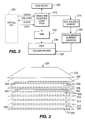
- FIG. 2 is a block diagram of image processing and driving circuitry suitable for use in the tile shown in FIGS. 1A and 1B.
- FIG. 3 is an exploded perspective drawing which illustrates an alternative structure that may be used to implement the tile shown in FIGS. 1A and 1B.
- FIG. 4 is a back plan view of a tile having the structure shown in FIG. 3 .
- FIG. 4A is a pixel diagram which shows an exemplary pixel layout for portions of four tiles having the structure shown in FIG. 3 .
- FIG. 5 is a pixel diagram which shows an alternate exemplary pixel layout for portions of four tiles having the structure.
- FIG. 6A is a front plan view of a single color pixel structure which includes separate sub-pixels.
- FIG. 6B is a front-plan view of an alternative single color pixel structure which includes separate sub-pixels.
- FIG. 7 is an exploded isometric drawing which illustrates an exemplary mounting method suitable for use with the tiled display shown in FIG. 1 .
- FIG. 8 is a cut-away side plan view of a portion of the tiled display shown in FIG. 1 which illustrates an exemplary method for joining adjacent tiles.
- FIG. 9 is a perspective view of a mullion suitable for use with the joining method shown in FIG. 8 .
- FIG. 10 is a cut-away side plan view of the glass plate of a pixel of a tile having the structure which is useful for describing a method for forming a black matrix for the tile.
- FIG. 11 is a cut-away side plan view of a portion of the glass plates of two adjacent tiles which shows how the tiles may be joined by a mullion such as that shown in FIG. 9 .
- FIG. 12 is a cut-away side plan view of the glass plate of two adjacent pixels of two adjacent tiles which is useful for describing a method for forming a black matrix for the display.
- FIG. 13 is a partially exploded perspective view of the tiled display shown in FIG. 1 which is useful for describing an exemplary mounting method and an exemplary implementation of a black matrix for the tiled display.
- FIG. 13A is a detailed view of a portion of the partially exploded perspective view shown in FIG. 13 .
- FIG. 14 is a side view of an exemplary video tile in which the electronics have been raised from the surface to improve heat dissipation and alleviate hot spots in the display.
- FIG. 15A is a side view of an exemplary video tile utilizing a fin structure to improve heat dissipation and alleviate hot spots in the display.
- FIG. 15B is a top view of the fin structure in FIG. 15 A.
- FIG. 16 is a side view of an exemplary video tile utilizing a flexible circuit board to improve heat dissipation and alleviate hot spots in the display.
- FIG. 17A is a top view of the first layer an exemplary video tile with the display section and electronic section coupled to the same side of a glass substrate.
- FIG. 17B is a top view of two layers the exemplary video tile of FIG. 17 A.
- FIG. 17C is a top view of three layers the exemplary video tile of FIG. 17 A.
- FIG. 17D is a top view of four layers the exemplary video tile of FIG. 17 A.
- FIG. 17E is a top view of five layers the exemplary video tile of FIG. 17 A.
- FIG. 17F is a top view of the complete exemplary video tile of FIG. 17 A.
- OLED optical light emitting diode
- LED light emitting diode
- BRC Reflective Cholesteric
- FIG. 1 is a front plan view of a partially assembled large-area display 100 according to the present invention.
- the display 100 is a tiled display in which emissive or reflective elements, on which the image pixels are formed, are built as relatively small arrays on tiles 120 and assembled into a frame to produce the large-area display having a large number of pixel forming elements.
- the tiles may be assembled side-to-side with their pixels aligned in rows and columns without a frame.
- the individual tiles may be held together by mullions.
- the tiles are constructed with pixel forming elements evenly spaced up to the edges of the tiles. As described below with reference to FIGS. 8 through 13, the tiles are formed such that, when they are joined, the inter-pixel distance between the edge pixels of two adjacent tiles is the same as the inter-pixel distance of adjacent pixels in the interior of a tile.
- the display shown in FIG. 1 is missing two tiles 122 and 124 . These tiles are inserted into the positions 102 and 104 to complete the display.
- each tile may include many more pixels.
- each tile includes 6400 pixel forming elements arranged as a 80 by 80 matrix. These tile sizes are only exemplary. It is contemplated that each tile may include more or fewer pixel forming elements.
- a single display may be formed from tiles having different numbers of pixel forming elements. For example, a display may have tiles with relatively large numbers of pixel forming elements near the center and tiles having relatively small numbers of pixel forming elements near the edges.
- FIGS. 1A and 1B are perspective drawings showing the back and front surfaces of an exemplary tile 120 .
- the tile includes a circuit board 130 on which is mounted at least one integrated circuit 134 .
- the integrated circuit is connected to the pixel forming elements through conductive traces 132 on the circuit board which are coupled to vias (not shown) that extend through the circuit board to make contact with the row or column electrodes of the display device.
- vias extend through the pixel forming elements internal to the display area, as described in U.S. patent application Ser. No. 09/250,324.
- the vias may extend through pixel forming elements along two edges of the display, as described below with reference to FIGS. 3 through 4A.
- the pixel forming elements are made from an organic light emitting diode (OLED) material.
- OLED organic light emitting diode
- the basic light emitting structure consists of a thin organic polymer layer sandwiched between a pair of appropriately selected and patterned electrodes. Current flowing from one electrode to the other electrode causes the organic polymer to emit light. At least one of the electrodes is desirably transparent to the emitted light.
- ITO Indium tin-oxide
- Conductive polymers such as polyaniline may also be used.
- OLED materials provide high brightness and high efficiency, and are relatively low cost materials.
- An exemplary display structure according to the present invention is formed in two parts: a display section and an electronics section. These two parts are made separately and then joined to form a complete tile.
- the display section consists of a transparent glass layer on which transparent column electrodes are deposited.
- the active (i.e., light emitting) medium, an OLED material in this exemplary embodiment, is deposited onto this layer in a pattern of individual pixels, or subpixels. Row electrodes are deposited as the final display layer. Additional layers such as blocking or passivation layers may be present to improve the function or life of the display layers.
- the transparent electrode is preferably the hole-injecting electrode and the other electrode is preferably the electron-injecting electrode.
- the OLED materials between the electrodes are preferably conjugated polymer materials that are applied in the desired pixel pattern by thick film processes, however, small molecule materials can alternatively be applied by various thin film deposition techniques.
- the layers are patterned so that there is electrical access to each row and column at one or more points.
- the pixel forming elements of the tiles may be any of a number of emissive devices such as electroluminescent elements, light emitting diodes, field emissive elements, plasma elements or cathodoluminescent elements.
- emissive devices such as electroluminescent elements, light emitting diodes, field emissive elements, plasma elements or cathodoluminescent elements.
- the electronics section is formed by punching or drilling vias through the circuit board and then printing or otherwise depositing the conductive traces on the circuit board.
- the conductive ink or paste used to form the conductive traces may also fill the vias.
- the vias make contact with the row and column electrodes of the display section when the electronics section and the display section are joined to form a tile.
- another exemplary embodiment of the present invention includes a pixel forming structure that is appropriate for applications in which either a reflective or low power display is needed.
- the substrate and the electronics of this new structure are essentially the same as described below for the OLED embodiments.
- the display layer in this alternative embodiment is a reflective display material.
- a Bistable, Reflective Cholesteric (BRC) liquid crystal material which provides for a low power, bistable display.
- BRC Bistable, Reflective Cholesteric
- the disclosed tile structure enables, for the first time, video-rate displays in large area BRC displays. These materials switch between a planar, reflective state and a relatively transparent focal conic state. Utilizing a black backing, these two states may appear colored and black.
- the BRC materials offer distinct advantages for large area tiled displays: the operation between a reflecting and transparent state, combined with a black back-plane makes possible bright, high contrast displays under a variety of lighting conditions; and the bistability also allows for maintaining static images with no power applied.
- One exemplary tile structure consists of a multilayer ceramic circuit board 132 that serves as a substrate upon which: the display material is mounted on the viewer side while the electronics 134 (active and passive) or drive or other functions are mounted mostly on the back side.
- Conductor elements 132 are printed on the individual layers to provide interconnections between the electronics and the display material, vias interconnect the con conductors in different layers; and connectors are provided on the back surface to connect to external power and signal sources.
- the tile structure may also have a structural layer(s) such as a high softening point metal or insulator to provide freedom from distortion during the processing of the ceramic materials, and/or thermal management during the operation of the display.
- the tile structure also contains a transparent layer (e.g. float glass) on the viewer surface to protect or contain the display material.
- a back panel structure is provided to mount the individual tiles and to provide electrical connection to the power and drive signals needed by each individual tile structure.
- the Multilayer ceramic circuit board 130 may be formed of layers of ceramic material.
- the layers are first formed and processed to form vias, conductors, and other features and then assembled in a stack taking care to carefully align each layer with those layers adjacent to it.
- Ceramic material here is meant in the broadest sense to include ceramics, glass ceramics, glass, and other high temperature insulating materials, such as alumina.
- the multiple layers together with the connectors and vias provide the basic function of a circuit board upon which active and passive electrical devices and circuits can be placed.
- the conductors 132 may be thin and/or thick film conductors formed by any of the standard processes including, for example plating, evaporation, sputtering, printing and laminating.
- the materials may be metals or organic conductors.
- the conductors may be patterned by processes that may include, for example, printing or photolithography. These conductor patterns are formed on the surfaces of the individual layers in the disclosed structure and connect to the vias to provide, according to the design of the device a means of interconnecting the electronics on and external to the disclosed structure to the display material.
- Via is used in the broadest sense and includes conductors that go through openings in the layers, including the substrate, and those that go around an edge of the layers. Vias that go through a layer can be formed, for example, by making a hole in the layer and filling that hole with a conductor. Alternatively, pre-formed physical conductors may be imbedded in the layer. Vias that go over the edge of the layers can be formed by physically placing a wire (round or flat), or array of wires, and wire bonding the ends to the surfaces to be interconnected. Alternatively they can be formed in place by plating or other fabrication process for thick or thin film conductors.
- the circuit board may by formed from a single ceramic material.
- a single material ceramic circuit board may be quite rugged depending on the material selected. This type of circuit board provides a single expansion coefficient, but may exhibit some difficulties with thermal management. Several exemplary methods to overcome this performance issue are discussed below in reference to FIGS. 14 through 16.
- a core layer may also be included in this structure.
- This layer serves as a substrate for the assembly and processing of the ceramic material.
- the core layer acts to eliminate horizontal shrinkage, establish a single coefficient of expansion for the multilayer system, and provide mechanical ruggedness to the multilayer assembly. If the layer is a good electrical conductor it may also provide RF shielding. If the layer is also a good thermal conductor, it contributes to the thermal management of the display.
- Conductive layers present a special problem for via connections. Via connections through metal layers can be fabricated in several ways: filling the periphery of the hole with an insulating material before putting a metal conductor through the middle, or by putting the conductor only through the middle leaving space separating the conductor from the conductive metal core.
- the electronics which form the image processing and pixel driving circuitry are mounted on the layers. Electronics are used in the broadest sense to include both active and passive devices, and both discrete devices mounted on the layers and devices formed in place by processes such as those now used to make active matrix circuits for displays on various high temperature substrates. While these electronics can be placed anywhere, the most convenient location is the back surface. This permits standard assembly and attachment equipment and processes to be used. In addition, the placing of active or passive devices on the intervening layers or viewer surface permits greater flexibility in the system design.
- the display material is applied to the surface visible to the viewer. Because of the flexibility of the construction of the disclosed structure, different display materials can be used.
- the display material is covered by a transparent layer to protect and contain the display material. Although for individual pixels this layer may be the transparent electrodes, it is often desirable to couple an additional, substantially flat layer of transparent material, such as float glass, over the electrodes and display material.
- edges of the tiles are desirably carefully formed to ensure that the tiled display has no visible seams between the tiles.
- One criterion for the tiles is that the spacing between the pixels separated by the tile seam is the same as the spacing of pixels on the tile.
- the tile edges are desirably dimensionally precise.
- the edges are also used for conductors or if mullions are used to join adjacent tiles, it is desirable to account for the thickness of these conductors or mullions in the design and placement of the tiles.
- a back panel may be provided for the physical mounting and interconnection of the tiles to form a display.
- the mounting of the tiles is done such that there is continuity in the pixel spacing over the display.
- the shape of the tiles is most typically square or rectangular, however the shape can be any shape that can be tiled to form a larger display.
- the tile is typically flat, but may be curved along one or both dimensions to form curved or domed displays. Curved or domed displays can also be made using flat tiles mounted on a curved or domed back panel.
- Tiles may be attached to the back panel either by permanent connection such as soldering or using connectors which allow the tiles to be plugged into the back panel. This latter method permits the repair and replacement of individual tiles.
- Different types of tiles may be attached to different areas of the back panel—for example, higher resolution areas may be placed in the center or other areas of the large display.
- different sized or different shaped tiles may be combined in a single display. For example, tiles near the edges of a large panel may be larger and have a lesser pixel density than tiles near the center of the panel.
- the back panel may also provide the means for connecting the tiles to the operational power and data signals needed to operate the tile.
- Matching connectors may be provided on both the back side of the tile and the back panel to provide this connection.
- optical connection may be used as an alternative to physical connection.
- the electrical structure of the back panel provides for the distribution of power and signals to the tiles, and the electrical structure of the tiles provide for the addressing of the display pixels. Both levels of structure are described.
- the information needs of a tiled display increase with the size of the display as measured in total number of pixels. If the tile includes image data storage, a greater number of pixels on a tile translates to greater amounts of data stored on the tile and greater rates of information transfer. If the image data is not stored on the tile then extra structures are used to provide the data for display in a timely manner.
- tiled display One advantage of the tiled display is that the scan electronics can be internal to the tile and the scan rate of any one tile is the same for a small display or for a large display. Including driving and timing circuitry on each tile may provide a method to ensure that the brightness and gray scale of the display do not degrade with increasing size.
- the tiled displays described in detail below have an architecture which connects the signals to the pixels without interrupting the continuity of the pixel spacing, even at the edges of the tiles.
- the disclosed tiled displays may also have signal processing circuitry which extracts the signal information for that tile from a broadcast information signal and transforms the extracted information into the signals needed to address the tile.
- exemplary display tiles of the present invention may include a memory used to store image data.
- the front-to-back connections include at least one for each row of pixels and at least one for each column of pixels on the tile.
- An exemplary embodiment of the present invention utilizes 10-20 connections per column and 4-8 connections per row.
- Tiled displays have relatively few pixels so that the number of interconnects per tile is relatively small and the yield on individual tiles can be high. This is a significant advantage of tiled displays when compared to fabrication of large displays from single substrates.
- the yield is a function of the number of pixels in the display device. The redundancy provided by adding more than one connection per row or column may further increase yield and reliability, and may also reduce line impedance for the rows and columns.
- connection to the row or column is made with a via that extends from the back surface of the tile.
- This via has a diameter less than the spacing of a pixel.
- the portions of the vias in the display layer(s) may be made smaller than the vias through the other intervening layers, and, as described below, the connections may be staggered over the area of the tile to provide maximum spacing between the wider interconnects. These connections are a link in the distribution of the display signals to the pixels.
- FIG. 2 is a block diagram of electronic circuitry which is suitable for use with a display tile according to the present invention.
- This figure illustrates three major elements of electronics mounted on the circuit board 120 of an exemplary embodiment of the present invention: a memory 212 ; pixel driving circuitry 214 , 216 , 218 and 220 ; and timing circuitry 210 .
- the operational power connections e.g. power and ground
- FIG. 2 illustrates three major elements of electronics mounted on the circuit board 120 of an exemplary embodiment of the present invention.
- the operational power connections e.g. power and ground
- the exemplary embodiment includes a field programmable gate array (FPGA) 210 which comprises the timing and sequence logic, and receives timing and control signals and an image data signal. As described below, these signals may be provided to the tile by an electrical wiring harness or through an optional optical interface 224 (shown in phantom).
- the timing and control signal includes a system clock signal, a synchronization signal, and control values which may change the functions performed by the display electronics.
- the timing and sequence logic circuitry 210 may provide a clock signal, CLOCK, to the optical interface 224 .
- the circuitry shown in FIG. 2 may be viewed as having four functions: loading and storing compensation data for an individual tile, loading and storing display data for the tile, displaying the stored data, and adjusting to compensate for changes in the brightness performance of individual pixels.
- each tile may be separately compensated to ensure that the displayed pixels of all tiles have a uniform brightness with uniform colors.
- the exemplary method for compensating the tiles is described in terms of an OLED display material. It is contemplated, however, that a similar method may be used with other types of emissive and light modulating display materials.
- the level of light emitted by a particular OLED pixel is a function of the level of current provided to that pixel.
- the brightness of each pixel in the display is controlled by controlling the magnitude of current that is supplied to that pixel during normal operation.
- each pixel is either turned on or off. Gray scale is achieved by changing the relative amount of time that each pixel is turned on.
- the amount of light emitted by a pixel when it is turned on is controlled by controlling the level of current applied to the pixel in the on state.
- the level of current applied to each pixel may be adjusted to match the amount of light emitted by the pixel to the amounts of light emitted by every other pixel in the display device.
- the pulse width of the pulse which drives the pixel is changed to modulate the brightness of the pixel when an image is being displayed on the tile.
- the exemplary embodiment of the invention employs a passive addressing technique within a block in which only one row of pixels is illuminated at any time.
- the scanning circuitry steps through each row on the tile and illuminates that row for a predetermined interval. Because each tile is individually scanned, all of the tiles may illuminate a row simultaneously Thus, each time a single tile refreshes its pixels, the entire display device also refreshes its pixels.
- the row selection circuitry 222 may be, for example, a conventional clocked shift register having a number of stages equal to the number of rows in the addressing block.
- the shift register clocks a single logic-high value through the rows of the addressing block. As the logic-high value is applied to each row, the pixels in that row are selected.
- the current applied to a pixel cell on the display device is controlled responsive to a value for the pixel cell that is stored in the non-volatile memory 214 .
- the addresses of the pixels on the line are applied to the memory 214 , which provides a number of compensation values to the programmable current sources 216 .
- the number of values provided equals the number of columns in the display device.
- Each value is applied to a respectively different programmable current source to provide respective current values to the pixels in the selected row.
- the programmable current sources are coupled to the column drivers 220 . When the column drivers are enabled, they condition the respective pixels in the row to provide a level of current, determined by a respective one of the programmable current sources 216 , to the OLED material.
- the display of pixel data is controlled by pulse-width modulating the current signals provided to the selected row of pixels.
- an optional random access memory 212 stores a number of pixel values which may, for example, correspond to the number of pixels on the tile.
- the timing and sequence logic 210 selects a row, fetches the line of data corresponding to the selected row and applies the selected data to the pulse width modulator (PWM) 218 .
- the PWM 218 converts the binary values into respective pulse widths and controls the column drivers to apply the current levels provided by the programmable current sources 216 to the column electrodes of the tile.
- the memory 212 may hold more or less data than would be required to operate the number of pixels on the tile. If the memory holds less data, then new data may need to be stored into the tile while previously stored data is being displayed. If the memory 212 holds more data, then the circuitry shown in FIG. 2 may display image data for a row of pixels from one image frame while a row of data from the next image frame is being loaded into the memory 212 . In general, it is contemplated that the various functions performed by the electronic circuitry shown in FIG. 2, such as loading compensation data, loading pixel data and displaying pixel data, may be performed concurrently.
- the timing and sequence logic 210 receives the timing and control signal and decodes the control signal to determine which functions are to be performed.
- each tile may be calibrated to a nominal brightness value by, for example, mounting the completed tile onto a test fixture which has a photocell corresponding to each pixel position.
- Each pixel is individually turned on and its brightness is compares to the nominal brightness and a control value for the pixel is applied to the programmable current source 216 for that pixel.
- the value applied to the current source 216 is stored into the non-volatile memory 214 .
- the tile may also include circuitry which automatically adjusts the pixel brightness to compensate for aging of the display material.
- This circuitry may, for example, allow a viewer to display a predetermined brightness value, select an individual tile and adjust the brightness value up or down to match the brightness of the selected tile to match its neighbors.
- the tile may include a small light sensor over one or more pixel positions which continually monitors the brightness of that pixel and adjusts the current level applied to that pixel—and the current levels applied to all of the other pixels on the display—to compensate for variations in pixel brightness due to aging of the display. To minimize the visibility of the light sensor, it may be placed away from the active pixel area so that it is responsive to scattered light.
- the circuitry 134 may include an all electronic compensation system which continually adjusts the brightness of individual pixels to compensate for aging.
- the inventor has determined that the decay in the brightness of an OLED pixel that occurs with aging can be predicted by measuring the current and time for a particular pixel, and integrating the product of current and time. This product can be fitted to a characteristic curve and used to adjust the drive current to predict a new drive current which restores the original brightness level of the pixel.
- the rate of decay for different pixels differs slightly, and the initial decay slope can be measured during burn in and used as a second order correction factor in the algorithm for calculating any change in drive current for that pixel.
- the exact form of this adjustment depends on the geometry of the pixels and the materials that are used to form the pixels. A suitable adjustment may be readily determined by one skilled in the art of designing OLED displays by monitoring the performance of an exemplary pixel over time.
- This algorithm can be incorporated in the electronics on the electronic drive block, and the result is that the brightness can be maintained at constant brightness automatically without manual adjustments.
- This proportionality constant varies for different pixel geometries and different OLED materials. It can be easily determined by one skilled in the art of designing OLED displays by monitoring the performance of an exemplary pixel over time.
- an external system of reestablishing the brightness uniformity may be employed.
- a system may, for example, incorporate a sensor that detects and measures individual pixel brightness and some means to communicate with the display electronics so that the correct drive voltage needed to establish the desired brightness can be stored in the display tile memory.
- any of these methods for adjusting the current applied to a pixel in order to maintain a predetermined brightness level may be combined with any other method either as a check or to augment the performance of the other method.
- the exemplary display device calibrates the brightness of the pixels using a method (i.e. current control) which is orthogonal to the method (i.e. pulse-width modulation) which is used to control the pixels to achieve gray scale.
- a method i.e. current control
- the method i.e. pulse-width modulation
- FIG. 3 is an exploded perspective drawing which illustrates an exemplary structure of a tile 120 .
- the exemplary tile shown in FIG. 3 may be formed as a separate electronics section and display section or it may be formed as a single structure.
- the connections to the row and column electrodes of the tile are made along two edges of the tile.
- the circuit board for the tile shown in FIG. 3 is the bottom layer 510 .
- This circuit board may include, for example, an electronics module such as the circuit 134 shown in FIG. 1 A and layers of interconnects to connect the components of the electronics module.
- the electronics module is coupled to the row and column electrodes of the display device through column vias 520 and row vias 522 . Only one row via 522 is shown in FIG. 3 .
- the circuit board is level 510 and optional levels 512 , 514 and 516 , shown in phantom, are interconnecting layers. These may be ceramic layers having vias to connect to higher layers and conductive traces painted or printed on one surface of the layer.
- one of the layers 512 or 514 may be a metal layer or an insulating structural substrate.
- Layer 516 is a ceramic layer having column vias 520 and row vias 522 . The row vias formed on the ceramic layer 516 connect to the row electrodes 524 of the exemplary display tile.
- the electronics section includes only the layer 510 and the optional layers 512 , 514 and 516 .
- the display material 526 is deposited on top of the row electrodes 524 .
- the display material 526 is illustrated as a solid sheet. This material, however, may be distinct electron injecting layers and distinct OLED cells deposited on the row electrodes. Using distinct cells of display material, physically and electrically separate from neighboring cells, as illustrated in FIGS. 4A, 5 , 6 A, 6 B, and 12 , increases display contrast by greatly reducing both electrical and optical crosstalk between pixels, and sub-pixels.
- the row electrodes may be formed from a metal; such as aluminum, titanium, tungsten, gold, or copper; from polysilicon; or from a multilayer structure including such conductors.
- the column electrodes 528 are formed on top of the display material 526 .
- the column electrodes are connected to the circuit board through the vias 520 which extend through each level of the display tile from level 510 through level 526 .
- Each column electrode is coupled to a respectively different via 520 .
- the column electrodes 528 are typically formed from a transparent conductive material such as indium-tin oxide (ITO) or polyaniline.
- level 530 formed above the column electrodes 528 may be an optical filter or it may be a patterned black matrix which covers the inactive areas of the display layer 526 with black lines while providing openings for the active elements of the display material.
- the final layer of the display tile shown in FIG. 3, is a float glass front cover 532 .
- the display section may be formed in the following manner. First, the filter or black matrix layer 530 is deposited on the float glass cover 532 . Next, the transparent column electrodes 528 are deposited, then the OLED materials are formed on the column electrodes and the row electrodes 522 are formed to cover the OLED materials.
- the exemplary separate electronics and display sections shown in FIG. 3 may be joined by bump-bonding the row and column vias along their edges or by inserting conductive elements, for example wires, into the row and column vias on one of the sections such that the conductive elements protrude from the vias. The conductive elements would then mate with the corresponding vias on the other section when the sections are joined.
- the tile structure shown in FIG. 3 may be formed by first preparing green tape blanks for the layers 510 , 512 , 514 and 516 . Next, the blanks are punched with holes through which the vias 520 and 522 will be formed. After the blanks are punched, they may be painted or printed with suitable conductive material to fill in the vias and to provide any conductive traces which may be needed to interconnect other circuitry in the display tile.
- the traces printed on the green tape sheet 516 may include the row electrodes 524 .
- This structure including layers 510 , 512 , 514 and 516 as well as the vias 520 and 522 and the row electrodes 524 is then laminated and fired to form a ceramic substrate for the circuit component of the display device.
- a planarization layer may be added to the ceramic substrate to improve surface smoothness and thereby assist in fabication of the pixel structures.
- the planarization layer may be formed of a number of materials that form a highly smooth surface, such as spin-on-glass.
- the display materials 526 are deposited on the row electrodes 524 .
- the column electrodes are formed on the tile using conventional processes for depositing ITO.
- the circuit board 510 may be planar ceramic material, such as alumina.
- OLED display layers are sensitive to water vapor and oxygen. These agents must be blocked from passing through the base substrate.
- An advantage of alumina is that it forms a satisfactory blocking layer. Vias may be fabricated in so that they also block water vapor and oxygen.
- the layers 512 , 514 , and 516 shown in FIG. 3 may not exist.
- layer 512 may be spin-on-glass.
- the spin-on-glass layer may be desirable as a planarization layer to improve surface smoothness and thereby assist in fabication of the pixel structures.
- the spin-on-glass layer may provide the additional advantage of being a blocking layer.
- the alumina circuit board may be machined, or otherwise worked by processes such as etching, to provide the necessary vias and the worked circuit board may then be processed in the same way as the fired ceramic circuit board described above.
- the black matrix or filter 530 may be formed on the float glass cover 532 .
- the combined mask and cover is then aligned with the display device such that the openings in the mask correspond to the active pixel regions of the display material.
- the glass cover 532 is then sealed to the alumina circuit board or composite fired ceramic structure using, for example, a frit glass.
- the pixel structures may be formed on the glass cover, as in the two section construction described above, and then aligned to the alumina circuit board or composite fired ceramic structure and sealed.
- FIGS. 17A-F are top view drawings showing an exemplary display tile of the present invention. Each successive figure shows an additional layer which has been added to the glass substrate. In this embodiment both the display section and the electronics section are formed on the same side of a single glass substrate without a separate circuit board for, the electronics section.
- the exemplary embodiment depicted in FIGS. 17A-F has only four pixels. The number of pixels shown has been selected for clarity in the drawings and is not meant to illustrate a constraint on the number of pixels that may be employed in a display tile constructed according to this embodiment of the present invention.
- FIG. 17A illustrates a black matrix mask 2010 that has been deposited on the inner surface of the glass substrate 532 .
- the black matrix mask is patterned to cover the entire inner surface of the glass substrate except for windows corresponding to the active pixel areas.
- the black matrix mask may be deposited on the outer surface of the glass substrate. In this case the black matrix mask may conform to the dimensions previously described with regard to FIGS. 10 and 11.
- FIG. 17B illustrates transparent column electrodes 528 which have been deposited on top of the black matrix mask 2010 .
- These electrodes may be composed of multiple layers. The electrodes are shown substantially matching the height of the windows in the black matrix mask. It is contemplated that the transparent column electrodes may be either smaller or larger than these windows. Portions of the electrodes that extend outside of windows may be opaque.
- FIG. 17C shows display material 526 which has been formed in patterned portions on top of the transparent column electrodes. Additionally a passivation layer, not shown, may be added to cover areas of the transparent electrodes 528 that are not covered by the display material to prevent contact between the row electrodes and the column electrodes.
- FIG. 17D shows row electrodes 522 which have been formed covering the display material 526 .
- the row electrodes similarly to the transparent column electrodes, may be formed by a multi-layer process or in a single layer of conductive material.
- FIG. 17E shows a passivation layer 1702 .
- This passivation layer is used to both electrically isolate and seal the layers of the display section, particularly the display material 526 .
- the passivation layer may be composed of either a transparent or opaque material and may cover the entire back surface of display tile 120 , although here it is illustrated as leaving a small gap along the edges uncovered.
- the passivation layer is patterned to contain vias through which connections may be made to both the transparent row electrodes 528 and the column electrodes 522 .
- FIG. 17F shows an electronics module 1704 mounted in section of display tile 120 directly over a portion of the glass substrate 532 which has been covered by the black matrix mask 2010 .
- This orientation of the electronics module insures that the electronics module is not visible to a viewer viewing the display. Also by placing the electronics module only in sections covered by the black matrix mask it may be possible to reduce the effect of possible hot spots caused by the electronics modules.
- contacts 1706 which extend from the electronics module to the gaps in the passivation layer 1702 and electrically couple the electronics modules to the row and column electrodes below.
- the electronics modules in FIG. 17F are shown disposed upon the passivation layer 1702 it is contemplated that the electronics modules may be coupled to the back side of the display tile in this embodiment by a method whereby the electronics modules are not in direct contact with the passivation layer such as by solder bumps or flip chip technology. In these cases the method of using long leads to assist with thermal management of the display tile may be employed in this embodiment. Further if the passivation layer 1702 is composed of an opaque material then the electronics modules may be arranged in areas which are not covered by the black matrix mask without becoming visible to viewers of the tiled display system.
- a protective layer may be deposited over the electronics section of the tile to seal the tile and protect the display materials from water vapor and oxygen.
- FIG. 4 is a bottom plan view of the display tile shown in FIG. 3 .
- the circuit board 510 includes electronic circuitry 134 ′ which is connected to the rows and columns of the display through the vias 520 and 522 respectively.
- the conductors 602 which connect the circuitry 134 ′ to the vias 520 and 522 may be printed or painted onto the green tape prior to firing, as described above. Alternatively, these vias may be painted or printed onto the worked alumina circuit board.
- the connectors 602 are coupled to the vias 520 and 522 along the edge of the circuitry 134 ′.
- the circuitry 134 ′ is coupled to receive operational power via conductors 610 and to receive the data signal and timing information via conductors 612 and a connector 614 .
- the connector 614 may be coupled to a cable harness when the tile 120 ′ is assembled into a tiled display device such as the device 100 shown in FIG. 1 .
- FIG. 4A is a pixel diagram which illustrates an exemplary pixel spacing that may be used in the tile shown in FIG. 3 .
- This pixel spacing allows the conductive vias to be arranged along the edge of the tile, without locally distorting the inter-pixel distance in the assembled tiled display.
- FIG. 4A illustrates portions of 4 tiles, 630 , 640 , 650 , and 660 .
- the dashed lines 624 and 622 illustrate tile boundaries. These lines are provided only as a guide in understanding the pixel layout.
- the active portion 526 of the pixels occupies only about 1 ⁇ 4 of the total pixel area. This defines a pixel aperture of approximately 25%. In this exemplary embodiment of the invention, the active region is not centered in the pixel area but is offset to the left and top as shown in FIG. 4 A.
- this spacing of the pixels leaves room along the edges of the display for the vias 520 and 522 to connect electronic driving circuits to the row and column electrodes of the pixel without interfering with the regular spacing of the pixels across tile boundaries.
- the vias may be placed such that they are not directly in contact with the row and column electrodes, but are otherwise electrically coupled to the electrodes. This electrical coupling may be accomplished by small tabs of metal or other electrode material extending from the electrodes, or by gold bonding, or other standard electronics practice. In the exemplary embodiment shown in FIG.
- the distance d e which is the distance from the active region 526 to the edge of the tile, is approximately twice the distance d I which is the internal distance from the edge of the active area of the pixel 526 to the pixel boundary 522 or 524 .
- the active region of the pixel offset both horizontally and vertically, it is contemplated that the active area may be offset only vertically.
- the contacts to the row electrodes are beneath the active pixel material and, thus, do not need to offset the active region of the pixel. It is also possible to stagger the vias and contacts to spatially separate the vias.
- FIG. 5 is an alternative pixel layout.
- the active portions 526 of the pixels are centered in their respective pixel regions and the vias which connect the row and column electrodes of the display to the electronics are formed between respective pixel elements.
- the distance between the edge of an active region 526 and the edge 712 of the display is equal on all sides of the tile and the distance from the center of the active pixel region to the edge is 1 ⁇ 2 of the pixel pitch.
- the distance between the center of an edge pixel and the edge of the tile may be slightly less than 1 ⁇ 2 of the pixel pitch in order to allow a mullion to be inserted between adjacent tiles.
- mullions are typically used both to join tiles on the display device and to hide the edges where the tiles meet.
- the displays described above have been, in general, monochrome displays.
- the pixels have a single emissive area which is controlled by a single row and column electrode pair.
- Color pixels may be implemented as shown in FIGS. 6A and 6B.
- FIG. 6A shows a single pixel having separate red (R) 820 , green (G) 822 and blue (B) 824 sub-pixels.
- the three sub-pixels 820 , 822 and 824 each has a respective column electrode (not shown) which may be connected to the electronics section by the vias 810 , 812 and 814 , respectively.
- only one of vias 810 , 812 , and 814 is formed within a given pixel.
- a single row electrode (not shown) is used by all three of the sub pixels. This row electrode is coupled to the electronics section by the via 816 , shown in phantom.
- the geometry of the triple sub-pixel structure is defined by d SH , the height of the sub-pixel, d SW , the width of the sub-pixel, and d e , the distance from the active sub-pixel areas to the edge of the pixel area. For one exemplary embodiment of the invention, these dimensions are given in Table 1 in terms of the pixel pitch, P.
- the number contact points layers for an electrode within the circuit board layers is not constrained by the number of vias. Multiple contact points may branch out from a single via.
- FIG. 6B illustrates an alternative color pixel structure.
- This structure includes four sub-pixel elements, 830 , 832 , 834 and 836 .
- two of these sub-pixel elements, 830 and 836 emit green light when stimulated while the other two pixel elements, 832 and 834 emit red and blue light, respectively.
- This structure is known as a quad sub-pixel structure.
- the structure uses two green sub-pixels because more of the luminance information in a color display is in the green pixels than is in either of the red or blue pixels. Thus, the use of two green sub-pixels allows for a brighter display.
- the pixels 830 and 836 may both be red or blue pixels.
- the amount of light emitted by the red or blue pixel material may be less than the amount of light emitted by the green pixels. In this instance, making the pixels 830 and 836 both red or blue pixels, respectively, would improve the overall brightness of the display. It is also contemplated that it may be desirable to use colors other than, or in addition to, red, blue, and green in some display technologies.
- the pixel structure shown in FIG. 6B employs two row electrodes (not shown) and two column electrodes (not shown). The row electrodes are coupled to the electronics section by the vias 816 ′ and 818 (shown in phantom) while the column electrodes are coupled to the electronics section by the vias 810 ′ and 812 ′.
- the geometry of the quad sub-pixel structure is defined by the dimensions d SH , the height of the sub-pixel, d SW , the width of the sub-pixel, d e , the distance from the active sub-pixel areas to the edge of the pixel area, and d SI the distance between adjacent sub-pixels. These values are defined in Table 2 for the exemplary embodiment of the invention.
- FIGS. 6A and 6B show the distances d e and d SI as being equal in the horizontal and vertical directions, it is contemplated that these values may be different.
- the exemplary pixel structures shown in FIGS. 6A and 6B both have active pixel portions covering approximately 25 percent of the pixel area to produce a pixel aperture of approximately 25 percent. This value is exemplary only. The invention contemplates both larger and smaller pixel apertures.
- FIG. 7 is an exploded front plan view of an exemplary self aligning tile assembly structure according to the present invention.
- the frame 1410 includes a plurality of spring elements 1418 .
- the power, timing, and data signals are brought to the individual tiles by respective flexible connectors 1416 .
- the connectors 1416 may also act to push the tile forward to make contact with a float-glass front plate (not shown).
- the connectors 1416 are coupled to receive the power, data and timing signals via a wiring harness 1422 .
- each of the tiles is mounted, within the frame 1410 , on its respective flexible connector 1416 .
- the edges of each tile may be formed in complementary patterns (not shown) such that the patterns of adjacent tiles mate, holding the tiles in alignment.
- complementary patterns such that the patterns of adjacent tiles mate, holding the tiles in alignment.
- opposite edges of a tile may be patterned with complementary serrated edges which allow each tile to mate with an adjacent tile in only one position. If the tiles are formed in two parts, it is contemplated that these edge patterns may be made on the display section or on the electronics section. Making the edge patterns only on the electronics section is desirable as it simplifies the edge fabrication for the display sections. If the tiles are formed on single substrates, the substrates may be formed with complementary edge patterns.
- FIGS. 8 through 13 illustrate another exemplary method by which tiles 120 may be joined to form a composite tiled display 100 .
- a black matrix may be fabricated from black lines, placed between the active portions of the pixels to absorb ambient light in these areas in order to increase the display contrast.
- Black matrix lines may be found, for example between the phosphors on the front screen of a CRT or between the pixel positions defined for a liquid crystal display.
- black matrix lines are typically smaller than mullions and are typically placed in the plane of the pixels. Because the black matrix lines are periodic and placed between the pixels, they do not tend to break the continuity of the image.
- FIGS. 13 and 13A An illustration of this structure is shown in FIGS. 13 and 13A.
- FIG. 13 is a cut-away perspective drawing of a partially assembled display device.
- FIG. 13A shows details of a portion of the display device shown in FIG. 13 .
- the main components of the structure shown in FIG. 13 are a frame 2014 , a transparent sheet 2020 of, for example, glass or plastic, a plurality of black lines 2010 that form a black matrix and the tiles 120 which form the display.
- the key feature of the optical integrator structure is a pattern of black lines 2010 which are similar to black matrix lines in that they have equal widths and a spacing equal to the pixel pitch. These black lines 2010 may be aligned to lie between all pixels in the display, including those pixels on either side of the gaps 2012 between the tiles 120 .
- the optical integrator pattern of black lines are also similar to mullions in that some of the black lines in the optical integrator structure lie on top of the gaps between the display tiles and block their visibility.
- the glass substrates 532 of the tiles 120 are positioned adjacent to the black lines 2010 on the back surface of the transparent sheet 2020 , which forms the integrating structure.
- the disclosed optical structure for integrating display tiles is placed above the plane containing the pixels (like mullion structures), on the viewer-side of the tiles 120 , with the black line pattern being in contact with the display tiles.
- the black lines on the optical integrator structure 2020 are relatively narrow, so that the black lines which cover the mullions are essentially the same width as the black lines which form the black matrix.
- the disclosed structure simultaneously provides the functions of the black matrix and the mullions, but the mullion lines are not visible, as such, to the viewer because all lines in the pattern on the optical integrator structure 2020 are essentially the same and are virtually indistinguishable. Accordingly, the viewer simply sees a uniform pattern of black lines.
- FIG. 8 is a cross section of portions of two tiles 120 , according to the present invention, which are joined by a mullion.
- Each of the tiles includes a glass substrate 532 and the remainder of the tile structure 1510 .
- the exemplary tiles include active display material 1514 located proximate to the bottom surface of the glass substrate 532 .
- the exemplary tiles also include a mullion 1512 and black lines 1513 which form a portion of the black matrix.
- FIG. 9 is a perspective drawing of an exemplary mullion 1512 suitable for use with a display device according to the subject invention.
- the mullion 1512 includes a top surface 1610 which may be formed from a black material or may be printed or painted black. To ensure that the mullion does not create artifacts on the display device, it is desirable for the top surface of the mullion to closely match the black stripes in size, color and gloss.
- the mullion 1512 also includes a bottom stem having side surfaces 1612 which are desirably formed from a light-colored material (e.g. white). Alternatively, the bottom stem of the mullion may be transparent and have an index of refraction close to that of the float glass substrate 532 .
- the bottom stem of the mullion prefferably be light-colored or transparent so that any light scattered in the vicinity of the mullion has the same properties as light that is scattered among pixels at the interior of a tile. If light scatters differently at the edge of a tile than near the center then the edge may be visible, for example, as a band of reduced brightness in the displayed image.
- One or more of the side surfaces 1612 and the underside 1614 of the top bar of the mullion may be coated with adhesive to attach the mullion 1512 to the two tiles which it joins. If all of these surfaces are coated with adhesive, the mullions may be used to join the tiles into a display device.
- FIG. 10 shows a cross section of an exemplary glass substrate 532 which includes a bottom surface 1710 and a top surface 1712 .
- a number of representative optical rays, 1714 , 1716 and 1718 are shown emanating from a point on the bottom surface 1710 .
- Some rays 1714 exit the glass and some rays 1718 are totally internally reflected from the top surface and are trapped in the sheet of glass.
- rays 1716 At the transition between these two types of rays are rays 1716 which are refracted to an angle parallel to the top surface 1712 of the substrate 532 .
- the angle of incidence of the rays 1716 which are at the transition is called the critical angle ( ⁇ c ).
- ⁇ c The angle of incidence of the rays 1716 which are at the transition.
- the critical angle is dependent on the index of refraction, n glass , of the glass substrate 532 as shown in equation (1):
- n glass 1.55 and ⁇ c ⁇ 40°.
- a tiled display is made of tiles that are placed in an array so that the spacing between pixels across the gap between tiles is substantially the same as the pitch between pixels within the display tires.
- the same black stripe blocks any external rays from making the gap region visible. Thus this black stripe makes the gap region invisible to an observer.
- the black stripe may need to be slightly wider than 2d c to account for any finite width of the gap.
- the individual tiles do not need to be joined by discrete mullions. Instead, the tiles may be assembled directly on the back surface of the optical integrating structure 2020 such that the gaps are positioned directly over black stripes having a width W m .
- the exemplary optical integrating structure 2020 is positioned on top of the array of tiles, with the black lines on the surface of the structure in contact with the glass substrates 532 of tiles. The centers of the black lines are aligned with the gaps between the tiles so that the gap regions can not be seen by an observer.
- the integrating structure 2020 may include black lines that cover the top surfaces 1610 of the mullions. In this instance it would be desirable for the top bar of the mullion to be as narrow as possible to minimize any gap between the top surface of the tile 120 and the back surface of the integrating structure 2020 .
- the mullions 1512 may be assembled onto the integrating structure 2020 with the black matrix lines. In this configuration, the mullions form pockets into which tiles 120 are inserted to form the composite display. This structure may be formed by attaching the mullions directly to the integrating structure 2020 using an adhesive and then applying an adhesive to the undersides of the crossbars 1610 and to the sides of the stems before inserting a tile into the display.
- the black lines on the optical integrating structure 2020 that form the mullions which are used to cover the inter-tile gap tend to be wider than the typical black matrix line and may block some or all of the light emitted from the pixels near the edge of the tile.
- the display tiles and the black stripes on the integrating structure 2020 are desirably specifically designed to have particular relationships.
- FIG. 12 shows a cross section of a pixel which includes two pixel regions.
- the emissive regions 1910 at the bottom of the glass substrate 532 have a width d p .
- the light rays that can exit the glass section and are useful for viewing, exit the top of the glass 532 in an area having a width w 2d c +d p .
- a display tile has an array of pixels equally spaced a distance known as P, the pixel pitch. Therefore, to not block any viewable light, it is desirable for the black matrix to have a width, W m ⁇ P ⁇ d p ⁇ 2d c .
- the dimensions illustrated in FIG. 12 depict the case where the black matrix stripe completely hides the gap and yet, blocks no emitted light.
- the thickness of the glass substrate 532 and the width of the black stripe satisfy the criteria described above, no light that is directed toward a viewer directly in front of the display (e. g. viewing from a normal angle) is blocked, and no light from greater viewing angles is blocked.
- the thickness of the glass substrate 532 and/or the width of the black stripe are greater than the criteria described above, no light that is directed toward a viewer directly in front of the display (e. g. viewing from a normal angle) is blocked, but some light from greater viewing angles may be blocked.
- the pixels on the tiles have an aperture of approximately 25% in order to allow room within the pixel for a via to make electrical contact with a column electrode.
- d p is approximately P/2. This relatively small aperture also has advantages by making it easier to hide the inter-tile gap and allowing a relatively large-stripe black matrix to improve the contrast of the display.
- the contrast may be further improved by coating the viewer-side of the integrating structure 2020 with an antireflection coating and/or by adding an ambient light absorber or color filter on that surface or in the bulk of the material (e.g. glass or plastic) from which the optical integrating structure 2020 is constructed.
- the integrating structure 2020 may include a diffuser coating on the viewer-side surface. This diffuser enlarges the apparent size of the pixels reducing the visibility of the individual pixels and black matrix structure. Thus, a diffuser may act to reduce the graininess of the displayed image. This may be significant, especially for display devices having relatively large pixels or which have smaller pixels but are designed to be viewed at close proximity to the display device.
- Another method by which the visibility of the pixel structure may be reduced is to use a quad pixel structure, such as that shown in FIG. 6B, in which spaced single-color sub-pixels form a single color pixel.
- the integrating structure 2020 also provides a simple way to align and mount the display tiles.
- the patterns on the integrating structure 2020 may be accurately aligned with the pixels using, for example moiré patterns, to position a tile and then the tile may be mounted onto the structure 2020 with an optically clear adhesive.
- FIGS. 14 through 16 illustrate exemplary methods to improve the thermal management of video tiles.
- Thermal management is an issue because the output intensity of many display materials is thermally sensitive. Electronic components on the circuit board may generate heat during operation of the video tile. When this heat cannot be dissipated, the tile may become warm which may lead to changes in the output characteristics of the tile. If the tile conducts heat well, this may not be a serious problem. With general heating of this sort it may be possible to compensate for the heating, or if all tiles heat evenly, the changes may go unnoticed.
- a greater issue is when the circuit board is a poor conductor of heat and the individual electronic components cause hot spots in the display, small regions that are significantly hotter than surrounding sections of the tile.
- hot spots are greater in tiles constructed directly on circuit boards with poor thermal conductivity, it is peculiar to tiles of this construction. In some cases the hot spots small enough in magnitude and extent to be compensated. In other cases compensation may be difficult and steps to avoid these hot spots are desirable.
- FIG. 14 is a side view of an exemplary video tile fabricated on a single substrate 2101 .
- pixel structures 2103 are sandwiched between one side of the substrate and a transparent front panel 2102 .
- electronics 2104 are coupled to the substrate by exceptionally long leads 2105 .
- FIG. 15A demonstrates another exemplary embodiment of the present invention which may be used to avoid hot spots in the substrate surface.
- the substrate 2101 once again has pixels 2103 sandwiched between the substrate and the transparent front panel 2102 .
- the electronics 2104 are separated from the surface of the substrate by a fin structure 2201 which is mounted directly on the substrate.
- FIG. 15B shows a top view of this fin structure 2201 including the electronics 2104 which have been mounted onto the fin structure. Also in this view can be seen the conductive traces 203 and the via 2202 which are used to electrically couple the fin structure to the substrate.
- the fin structure itself works as a heat sink to dissipate heat, thereby preventing formation of hot spots in the substrate ensuring more uniform performance of the video tile.
- FIG. 16 demonstrates another exemplary embodiment of the present invention in which the single substrate 2101 , transparent front panel 2102 and pixels 2103 have the same functions as in the previous two embodiments which were illustrated in FIGS. 14 and 15A.
- a flexible circuit board 2301 has been connected to the back of the single substrate.
- One end of the flexible circuit board 2302 has been bent away from the surface of the substrate.
- the electronics 2104 are mounted. This is done once again to alleviate hot spots in the substrate.
Abstract
Description
| TABLE 1 | |||
| dSH | .5 P | ||
| dSW | .16 P | ||
| de | .25 P | ||
| TABLE 2 | |||
| dSH | .25 P | ||
| dSW | .25 P | ||
| de | .125 P | ||
| dSI | .25 P | ||
Claims (41)
Priority Applications (6)
| Application Number | Priority Date | Filing Date | Title |
|---|---|---|---|
| US09/709,904 US6498592B1 (en) | 1999-02-16 | 2000-11-10 | Display tile structure using organic light emitting materials |
| EP01988262A EP1332487A4 (en) | 2000-11-10 | 2001-11-09 | Display tile structure using organic light emitting materials |
| EP11155128A EP2330627A3 (en) | 2000-11-10 | 2001-11-09 | Display Tile Structure using Organic Light Emitting Materials |
| JP2002548911A JP2004515810A (en) | 2000-11-10 | 2001-11-09 | Display tile structure using organic light emitting material |
| PCT/US2001/046455 WO2002047310A2 (en) | 2000-11-10 | 2001-11-09 | Display tile structure using organic light emitting materials |
| JP2008312310A JP5219764B2 (en) | 2000-11-10 | 2008-12-08 | Display tile structures using organic light emitting materials |
Applications Claiming Priority (2)
| Application Number | Priority Date | Filing Date | Title |
|---|---|---|---|
| US09/250,324 US6897855B1 (en) | 1998-02-17 | 1999-02-16 | Tiled electronic display structure |
| US09/709,904 US6498592B1 (en) | 1999-02-16 | 2000-11-10 | Display tile structure using organic light emitting materials |
Related Parent Applications (1)
| Application Number | Title | Priority Date | Filing Date |
|---|---|---|---|
| US09/250,324 Continuation-In-Part US6897855B1 (en) | 1998-02-17 | 1999-02-16 | Tiled electronic display structure |
Publications (1)
| Publication Number | Publication Date |
|---|---|
| US6498592B1 true US6498592B1 (en) | 2002-12-24 |
Family
ID=24851777
Family Applications (1)
| Application Number | Title | Priority Date | Filing Date |
|---|---|---|---|
| US09/709,904 Expired - Lifetime US6498592B1 (en) | 1999-02-16 | 2000-11-10 | Display tile structure using organic light emitting materials |
Country Status (4)
| Country | Link |
|---|---|
| US (1) | US6498592B1 (en) |
| EP (2) | EP1332487A4 (en) |
| JP (2) | JP2004515810A (en) |
| WO (1) | WO2002047310A2 (en) |
Cited By (135)
| Publication number | Priority date | Publication date | Assignee | Title |
|---|---|---|---|---|
| US20020070909A1 (en) * | 2000-11-22 | 2002-06-13 | Mitsuru Asano | Active matrix type display apparatus |
| US20020140655A1 (en) * | 2001-04-03 | 2002-10-03 | Wei-Chen Liang | Pixel driving module of liquid crystal display |
| US20020140629A1 (en) * | 2001-03-28 | 2002-10-03 | Sundahl Robert C. | Method and apparatus for tiling multiple display elements to form a single display |
| US20020149598A1 (en) * | 2001-01-26 | 2002-10-17 | Greier Paul F. | Method and apparatus for adjusting subpixel intensity values based upon luminance characteristics of the subpixels for improved viewing angle characteristics of liquid crystal displays |
| US20020163527A1 (en) * | 2001-05-04 | 2002-11-07 | Park Dong S. | Method for adjusting brightness, contrast and color in a displaying apparatus |
| US20020167473A1 (en) * | 2001-04-26 | 2002-11-14 | Johnson Mark Thomas | Display device |
| US20020169571A1 (en) * | 2001-05-09 | 2002-11-14 | Decaro Robert E. | System for current matching in integrated circuits |
| US20020167475A1 (en) * | 2001-05-09 | 2002-11-14 | Dennehey Patrick N. | System for current balancing in visual display devices |
| US20030011724A1 (en) * | 2001-07-16 | 2003-01-16 | Sundahl Robert C. | Repairable tiled displays |
| US20030025450A1 (en) * | 2001-08-01 | 2003-02-06 | Hiroyuki Katayama | LED lamp and LED lamp manufacturing method |
| US20030025657A1 (en) * | 2001-08-03 | 2003-02-06 | Toshiaki Iwafuchi | Light emitting unit |
| US20030057895A1 (en) * | 2001-09-07 | 2003-03-27 | Semiconductor Energy Laboratory Co., Ltd. | Light emitting device and method of driving the same |
| US20030122813A1 (en) * | 2001-12-28 | 2003-07-03 | Pioneer Corporation | Panel display driving device and driving method |
| US20030141807A1 (en) * | 2001-01-31 | 2003-07-31 | Takeo Kawase | Display device |
| US20030173891A1 (en) * | 2001-06-13 | 2003-09-18 | Yasuhiro Chiba | Tie-ring type display device, and method of manufacturing the display device |
| US20030209977A1 (en) * | 2002-05-10 | 2003-11-13 | Ponnusamy Palanisamy | Thermal management in electronic displays |
| US20030222893A1 (en) * | 2002-05-30 | 2003-12-04 | Lockheed Martin Corporation | Light emitting diode display and method for the illumination thereof |
| US20030234343A1 (en) * | 2002-06-19 | 2003-12-25 | Eastman Kodak Company | Tiled electro-optic imaging device |
| US20040012330A1 (en) * | 2002-07-18 | 2004-01-22 | Tohoku Pioneer Corporation | Organic electroluminescent display device |
| US20040016568A1 (en) * | 2002-05-10 | 2004-01-29 | Ponnusamy Palanisamy | Low-cost circuit board materials and processes for area array electrical interconnections over a large area between a device and the circuit board |
| US20040032205A1 (en) * | 2002-08-16 | 2004-02-19 | Michael Hack | Organic light emitting devices for illumination |
| US20040036078A1 (en) * | 2002-06-20 | 2004-02-26 | Seiko Epson Corporation | Semiconductor device, method of manufacturing the same, electro-optic device and electronic apparatus |
| US6734617B2 (en) * | 2001-03-28 | 2004-05-11 | Intel Corporation | Stiffening flat-panel displays |
| US20040113875A1 (en) * | 2002-12-16 | 2004-06-17 | Eastman Kodak Company | Color oled display with improved power efficiency |
| US20040140960A1 (en) * | 2003-01-17 | 2004-07-22 | Eastman Kodak Company | OLED display and touch screen |
| US20040189559A1 (en) * | 2003-03-31 | 2004-09-30 | An Shih | Method and system for testing driver circuits of amoled |
| US6803892B2 (en) * | 2002-04-02 | 2004-10-12 | Samsung Electronics Co., Ltd. | Apparatus and method for controlling automatic adjustment of power supply of display panel driving system |
| US20040222954A1 (en) * | 2003-04-07 | 2004-11-11 | Lueder Ernst H. | Methods and apparatus for a display |
| EP1480195A1 (en) * | 2003-05-23 | 2004-11-24 | Barco N.V. | Method of displaying images on a large-screen organic light-emitting diode display, and display used therefore |
| US20040252076A1 (en) * | 2003-03-31 | 2004-12-16 | Yoshiyuki Kodama | Display device, electronic device and display method |
| US20040257007A1 (en) * | 1997-12-17 | 2004-12-23 | Color Kinetics, Incorporated | Geometric panel lighting apparatus and methods |
| US20040257352A1 (en) * | 2003-06-18 | 2004-12-23 | Nuelight Corporation | Method and apparatus for controlling |
| US20050052141A1 (en) * | 2003-04-24 | 2005-03-10 | Robbie Thielemans | Organic light-emitting diode drive circuit for a display application |
| US20050062680A1 (en) * | 2003-08-04 | 2005-03-24 | Samsung Electronics Co., Ltd. | Method and apparatus for compensating for difference in picture quality caused by burn-in effect on screen of display device |
| US20050077615A1 (en) * | 2003-10-10 | 2005-04-14 | Gang Yu | Heat sinks |
| US20050099411A1 (en) * | 2003-11-12 | 2005-05-12 | Van Brocklin Andrew L. | Large area display and method of manufacturing same |
| US6894665B1 (en) * | 2000-07-20 | 2005-05-17 | Micron Technology, Inc. | Driver circuit and matrix type display device using driver circuit |
| US20050116667A1 (en) * | 2001-09-17 | 2005-06-02 | Color Kinetics, Incorporated | Tile lighting methods and systems |
| US20050116921A1 (en) * | 2003-11-27 | 2005-06-02 | Kim Tae-Soo | Field sequential liquid crystal display |
| US20050134526A1 (en) * | 2003-12-23 | 2005-06-23 | Patrick Willem | Configurable tiled emissive display |
| EP1550947A2 (en) * | 2003-12-23 | 2005-07-06 | Barco N.V. | Configurable tiled emissive display |
| US20050156831A1 (en) * | 2002-04-23 | 2005-07-21 | Semiconductor Energy Laboratory Co., Ltd. | Light emitting device and production system of the same |
| US20050185114A1 (en) * | 2004-02-24 | 2005-08-25 | Eastman Kodak Company | Method for manufacturing a tiled display and tiled display comprising faceplate |
| US6940501B2 (en) * | 2001-03-28 | 2005-09-06 | Intel Corporation | Tiled display |
| US20050200294A1 (en) * | 2004-02-24 | 2005-09-15 | Naugler W. E.Jr. | Sidelight illuminated flat panel display and touch panel input device |
| US20050200292A1 (en) * | 2004-02-24 | 2005-09-15 | Naugler W. E.Jr. | Emissive display device having sensing for luminance stabilization and user light or touch screen input |
| US20050200296A1 (en) * | 2004-02-24 | 2005-09-15 | Naugler W. E.Jr. | Method and device for flat panel emissive display using shielded or partially shielded sensors to detect user screen inputs |
| US20050200293A1 (en) * | 2004-02-24 | 2005-09-15 | Naugler W. E.Jr. | Penlight and touch screen data input system and method for flat panel displays |
| WO2004094896A3 (en) * | 2003-04-21 | 2005-09-22 | Color Kinetics Inc | Tile lighting methods and systems |
| US20050225519A1 (en) * | 2004-04-12 | 2005-10-13 | The Board Of Trustees Of The Leland Stanford Junior University | Low power circuits for active matrix emissive displays and methods of operating the same |
| US20050243023A1 (en) * | 2004-04-06 | 2005-11-03 | Damoder Reddy | Color filter integrated with sensor array for flat panel display |
| US20050248286A1 (en) * | 2004-05-10 | 2005-11-10 | Dae-Young Yoo | Method for increasing durability of organic light emitting diode panel |
| US20050248515A1 (en) * | 2004-04-28 | 2005-11-10 | Naugler W E Jr | Stabilized active matrix emissive display |
| US20050248935A1 (en) * | 2004-05-04 | 2005-11-10 | Eastman Kodak Company | Tiled flat panel lighting system |
| US20050264149A1 (en) * | 2004-06-01 | 2005-12-01 | Eastman Kodak Company | Uniformity and brightness measurement in OLED displays |
| US20050280615A1 (en) * | 2004-06-16 | 2005-12-22 | Eastman Kodak Company | Method and apparatus for uniformity and brightness correction in an oled display |
| US20060077200A1 (en) * | 2004-10-13 | 2006-04-13 | Sony Corporation | Method and apparatus for processing information, recording medium, and computer program |
| US20060077193A1 (en) * | 2004-10-07 | 2006-04-13 | Robbie Thielemans | Intelligent lighting module and method of operation of such an intelligent lighting module |
| US20060108915A1 (en) * | 2004-11-23 | 2006-05-25 | Eastman Kodak Company | Tiled OLED display |
| US20060108913A1 (en) * | 2004-11-23 | 2006-05-25 | Eastman Kodak Company | Tiled display |
| US20060108918A1 (en) * | 2004-11-24 | 2006-05-25 | Eastman Kodak Company | Tiled OLED display |
| US7091927B1 (en) * | 2003-06-26 | 2006-08-15 | Rockwell Collins, Inc. | Display including tiles and a method of operating and manufacturing the same |
| US20060202924A1 (en) * | 2000-09-08 | 2006-09-14 | Semiconductor Energy Laboratory Co., Ltd. | Spontaneous light emitting device and driving method thereof |
| US20060290618A1 (en) * | 2003-09-05 | 2006-12-28 | Masaharu Goto | Display panel conversion data deciding method and measuring apparatus |
| EP1754121A2 (en) * | 2004-03-15 | 2007-02-21 | Color Kinetics Incorporated | Methods and systems for providing lighting systems |
| US7184067B2 (en) | 2003-03-13 | 2007-02-27 | Eastman Kodak Company | Color OLED display system |
| US7206005B2 (en) * | 2000-02-25 | 2007-04-17 | International Business Machines Corporation | Image display device and method for displaying multi-gray scale display |
| US20070086912A1 (en) * | 1997-08-26 | 2007-04-19 | Color Kinetics Incorporated | Ultraviolet light emitting diode systems and methods |
| US20070206148A1 (en) * | 2006-03-02 | 2007-09-06 | Mitsubishi Electric Corporation | Large-sized display apparatus and display device and display module used in large-sized display apparatus |
| US20070218751A1 (en) * | 2004-03-11 | 2007-09-20 | Element Labs, Inc. | Mounting system for light tiles attached to tensioned cables |
| US20070236431A1 (en) * | 2006-03-08 | 2007-10-11 | Sony Corporation | Light-emitting display device, electronic apparatus, burn-in correction device, and program |
| US20080048946A1 (en) * | 2006-08-23 | 2008-02-28 | Kwak Won K | Organic light emitting display device and mother substrate of the same |
| US20080054798A1 (en) * | 2006-08-30 | 2008-03-06 | Jin-Tae Jeong | Organic light emitting display device and mother substrate of the same |
| US20080121941A1 (en) * | 2002-12-31 | 2008-05-29 | Transmeta Corporation | Diagonal deep well region for routing body-bias voltage for MOSFETS in surface well regions |
| US20080136499A1 (en) * | 2002-12-31 | 2008-06-12 | Burr James B | Selective coupling of voltage feeds for body bias voltage in an integrated circuit device |
| US7397485B2 (en) | 2002-12-16 | 2008-07-08 | Eastman Kodak Company | Color OLED display system having improved performance |
| US20080218451A1 (en) * | 2007-03-07 | 2008-09-11 | Hitachi Displays, Ltd. | Organic electroluminescence display |
| US20080246110A1 (en) * | 2004-03-31 | 2008-10-09 | Transmeta Corporation | Structure for spanning gap in body-bias voltage routing structure |
| US20090050924A1 (en) * | 2007-06-11 | 2009-02-26 | Cree, Inc. | Droop-free high output light emitting devices and methods of fabricating and operating same |
| US20090067749A1 (en) * | 2006-01-13 | 2009-03-12 | Fraunhofer-Gesellschaft Zur Forderung Der Angewandten Forschung E.V. | Calibration Method and Calibration System for Projection Apparatus |
| US7543956B2 (en) | 2005-02-28 | 2009-06-09 | Philips Solid-State Lighting Solutions, Inc. | Configurations and methods for embedding electronics or light emitters in manufactured materials |
| US20090309819A1 (en) * | 2008-06-13 | 2009-12-17 | Element Labs, Inc. | Collapsible Support Structure for a Display |
| US20090313591A1 (en) * | 2004-02-03 | 2009-12-17 | Michael Pelham | Method for generating a deep n-well pattern for an integrated circuit design |
| US20100039779A1 (en) * | 2008-08-15 | 2010-02-18 | Siemens Power Generation, Inc. | Wireless Telemetry Electronic Circuit Board for High Temperature Environments |
| US20100090934A1 (en) * | 2008-04-15 | 2010-04-15 | Element Labs, Inc. | Isolating alignment and structural strength in led display systems |
| US7747974B1 (en) | 2003-10-10 | 2010-06-29 | Burr James B | Method and apparatus for optimizing body bias connections in CMOS circuits using a deep n-well grid structure |
| US20100170179A1 (en) * | 2007-05-25 | 2010-07-08 | Tru Woods Limited | Floor member |
| US7777691B1 (en) * | 2004-03-05 | 2010-08-17 | Rockwell Collins, Inc. | System and method for driving multiple tiled displays from a single digital video source |
| US7797655B1 (en) | 2005-07-28 | 2010-09-14 | Michael Pelham | Using standard pattern tiles and custom pattern tiles to generate a semiconductor design layout having a deep well structure for routing body-bias voltage |
| US20100277064A1 (en) * | 2009-04-30 | 2010-11-04 | Cok Ronald S | Tiled electroluminescent device with filled gaps |
| USRE41914E1 (en) | 2002-05-10 | 2010-11-09 | Ponnusamy Palanisamy | Thermal management in electronic displays |
| US20100309185A1 (en) * | 2009-06-05 | 2010-12-09 | Koester Robert D | Low-power and lightweight high-resolution display |
| US7864136B2 (en) | 1998-02-17 | 2011-01-04 | Dennis Lee Matthies | Tiled electronic display structure |
| US7990403B2 (en) | 2001-06-11 | 2011-08-02 | Genoa Color Technologies Ltd. | Device, system and method for color display |
| US20110204038A1 (en) * | 2010-02-23 | 2011-08-25 | Beijing Funate Innovation Technology Co., Ltd. | Heating tile and heated floor using the same |
| US20110267328A1 (en) * | 2010-04-28 | 2011-11-03 | Narayanan Venkatasubramanian | Failsafe interconnect for tiled wall display |
| US20110298396A1 (en) * | 2001-02-08 | 2011-12-08 | Semiconductor Energy Laboratory Co., Ltd. | Light Emitting Device and Electronic Equipment Using the Same |
| US8228275B2 (en) | 2003-01-28 | 2012-07-24 | Genoa Color Technologies Ltd. | Optimal subpixel arrangement for displays with more than three primary colors |
| US8289266B2 (en) | 2001-06-11 | 2012-10-16 | Genoa Color Technologies Ltd. | Method, device and system for multi-color sequential LCD panel |
| US20130026513A1 (en) * | 2011-07-25 | 2013-01-31 | Deeder Aurongzeb | Oled assembly and luminaire with removable diffuser |
| US20130082988A1 (en) * | 2011-09-29 | 2013-04-04 | Lg Display Co., Ltd. | Display Device |
| US20130101251A1 (en) * | 2011-10-24 | 2013-04-25 | Hitachi, Ltd. | Optical Module and Multilayer Substrate |
| WO2013062707A1 (en) * | 2011-10-28 | 2013-05-02 | Apple Inc. | Display with vias for concealed printed circuit and component attachment |
| US20130301195A1 (en) * | 2012-05-09 | 2013-11-14 | Wintek Corporation | Touch display device and driving method thereof |
| US8587621B2 (en) | 2005-11-28 | 2013-11-19 | Genoa Color Technologies Ltd. | Sub-pixel rendering of a multiprimary image |
| US8760877B2 (en) * | 2008-12-09 | 2014-06-24 | Koninklijke Philips N.V. | Flexible modular assembly |
| US8935867B2 (en) | 2008-06-13 | 2015-01-20 | Barco, Inc. | Angle and alignment adjusting method for a display |
| US9013102B1 (en) | 2009-05-23 | 2015-04-21 | Imaging Systems Technology, Inc. | Radiation detector with tiled substrates |
| US9214507B2 (en) | 2012-08-17 | 2015-12-15 | Apple Inc. | Narrow border organic light-emitting diode display |
| US9226347B2 (en) | 2012-06-25 | 2015-12-29 | Apple Inc. | Displays with vias |
| US9295131B2 (en) | 2012-03-08 | 2016-03-22 | Oledworks Gmbh | Segmented electroluminescent device with distributed load elements |
| US9361059B2 (en) | 2012-12-14 | 2016-06-07 | Intel Corporation | Architecture for seamless integrated display system |
| US9419065B2 (en) | 2012-08-07 | 2016-08-16 | Apple Inc. | Flexible displays |
| US9430974B2 (en) | 2001-06-11 | 2016-08-30 | Samsung Display Co., Ltd. | Multi-primary display with spectrally adapted back-illumination |
| US9431623B2 (en) | 2008-02-07 | 2016-08-30 | Qd Vision, Inc. | Flexible devices including semiconductor nanocrystals, arrays, and methods |
| US20160252996A1 (en) * | 2014-09-16 | 2016-09-01 | Boe Technology Group Co., Ltd. | Array substrate, in-cell touch screen and touch display device |
| TWI550849B (en) * | 2014-05-29 | 2016-09-21 | Organic light emitting diode device | |
| US9454025B2 (en) | 2012-08-31 | 2016-09-27 | Apple Inc. | Displays with reduced driver circuit ledges |
| US9504124B2 (en) | 2013-01-03 | 2016-11-22 | Apple Inc. | Narrow border displays for electronic devices |
| US9516743B2 (en) | 2013-02-27 | 2016-12-06 | Apple Inc. | Electronic device with reduced-stress flexible display |
| JP2016206542A (en) * | 2015-04-27 | 2016-12-08 | 日本放送協会 | Multi-split driving display and display device |
| JP2016206543A (en) * | 2015-04-27 | 2016-12-08 | 日本放送協会 | Multi-split driving display and display device |
| US9614168B2 (en) | 2015-01-12 | 2017-04-04 | Apple Inc. | Flexible display panel with bent substrate |
| TWI581226B (en) * | 2015-12-25 | 2017-05-01 | 正昌新視界股份有限公司 | A flexible led display |
| US9953590B2 (en) | 2002-04-11 | 2018-04-24 | Samsung Display Co., Ltd. | Color display devices and methods with enhanced attributes |
| US10261370B2 (en) | 2011-10-05 | 2019-04-16 | Apple Inc. | Displays with minimized border regions having an apertured TFT layer for signal conductors |
| TWI682531B (en) * | 2019-06-04 | 2020-01-11 | 友達光電股份有限公司 | Display apparatus and manufacturing method thereof |
| US10593743B2 (en) | 2016-12-30 | 2020-03-17 | Lg Display Co., Ltd. | Light emitting diode display device and multi-screen display device using the same |
| US11164934B2 (en) * | 2019-03-12 | 2021-11-02 | X Display Company Technology Limited | Tiled displays with black-matrix support screens |
| US20210398479A1 (en) * | 2020-06-23 | 2021-12-23 | Samsung Electronics Co., Ltd. | Light emitting diode package and display apparatus including the same |
| US11250769B2 (en) * | 2020-03-31 | 2022-02-15 | Shenzhen China Star Optoelectronics Semiconductor Display Technology Co., Ltd. | Compensation system and compensation method for life attenuation of OLED device |
| US11282474B1 (en) * | 2019-01-15 | 2022-03-22 | Rockwell Collins, Inc. | Systems and methods for multi-region displays |
| US20220139292A1 (en) * | 2020-11-02 | 2022-05-05 | Samsung Display Co., Ltd. | Display apparatus and method of driving the same |
| US11398181B2 (en) * | 2020-01-03 | 2022-07-26 | Samsung Electronics Co., Ltd. | Display module and driving method thereof |
| WO2023119251A1 (en) * | 2021-12-23 | 2023-06-29 | Vuereal Inc. | Seamless tiling |
Families Citing this family (16)
| Publication number | Priority date | Publication date | Assignee | Title |
|---|---|---|---|---|
| DE10262143B4 (en) * | 2002-12-20 | 2011-01-20 | Ksg Leiterplatten Gmbh | Light-emitting arrangement |
| EP1469450A1 (en) * | 2003-04-18 | 2004-10-20 | Barco N.V. | Organic light-emitting diode display assembly for use in a large-screen display |
| US7177064B2 (en) * | 2004-06-11 | 2007-02-13 | Lg Chem, Ltd. | Display device using printed circuit board as substrate of display panel |
| JP2007140071A (en) * | 2005-11-17 | 2007-06-07 | International Cooperation Of Economy Inc | Display device |
| DK2023187T3 (en) * | 2007-08-06 | 2013-01-28 | Barco Nv | Stitching hides for panel dividers |
| JP2009288741A (en) * | 2008-06-02 | 2009-12-10 | Mitsubishi Electric Corp | Image display device |
| US8125418B2 (en) * | 2009-06-26 | 2012-02-28 | Global Oled Technology Llc | Passive-matrix chiplet drivers for displays |
| US8081177B2 (en) * | 2009-08-28 | 2011-12-20 | Global Oled Technology Llc | Chiplet display with optical control |
| WO2013105347A1 (en) * | 2012-01-10 | 2013-07-18 | ソニー株式会社 | Display device and display method |
| NL2008316C2 (en) * | 2012-02-20 | 2013-08-21 | Ambianti B V | Adaptable building panel with electric devices. |
| US8974077B2 (en) | 2012-07-30 | 2015-03-10 | Ultravision Technologies, Llc | Heat sink for LED light source |
| TWI490837B (en) * | 2012-10-19 | 2015-07-01 | 啟耀光電股份有限公司 | Display apparatus |
| US9195281B2 (en) | 2013-12-31 | 2015-11-24 | Ultravision Technologies, Llc | System and method for a modular multi-panel display |
| GB2531558B (en) * | 2014-10-22 | 2021-01-13 | Facebook Tech Llc | Display |
| GB2586423B (en) * | 2014-10-22 | 2021-09-01 | Facebook Tech Llc | Display |
| DE102016124983A1 (en) | 2016-12-20 | 2018-06-21 | Osram Opto Semiconductors Gmbh | VIDEO WALL MODULE |
Citations (61)
| Publication number | Priority date | Publication date | Assignee | Title |
|---|---|---|---|---|
| US3828215A (en) | 1972-06-30 | 1974-08-06 | Ibm | Integrated packaging arrangement for gas panel display device |
| US3855499A (en) | 1972-02-25 | 1974-12-17 | Hitachi Ltd | Color display device |
| US4006383A (en) | 1975-11-28 | 1977-02-01 | Westinghouse Electric Corporation | Electroluminescent display panel with enlarged active display areas |
| US4155030A (en) | 1977-12-19 | 1979-05-15 | International Business Machines Corporation | Multicolor display device using electroluminescent phosphor screen with internal memory and high resolution |
| US4206460A (en) | 1977-03-10 | 1980-06-03 | Sharp Kabushiki Kaisha | EL Display drive controlled by an electron beam |
| US4266223A (en) | 1978-12-08 | 1981-05-05 | W. H. Brady Co. | Thin panel display |
| US4368467A (en) | 1980-02-29 | 1983-01-11 | Fujitsu Limited | Display device |
| US4471263A (en) | 1982-03-08 | 1984-09-11 | Burroughs Corporation | Buttable display panels |
| US4508990A (en) | 1982-09-17 | 1985-04-02 | Sigmatron Associates | Thin-film EL panel mounting unit |
| US4528480A (en) | 1981-12-28 | 1985-07-09 | Nippon Telegraph & Telephone | AC Drive type electroluminescent display device |
| US4554485A (en) | 1982-05-20 | 1985-11-19 | Matsushita Electric Industrial Co., Ltd. | Solid-state image display device |
| US4603280A (en) | 1984-10-30 | 1986-07-29 | Rca Corporation | Electroluminescent device excited by tunnelling electrons |
| US4613793A (en) | 1984-08-06 | 1986-09-23 | Sigmatron Nova, Inc. | Light emission enhancing dielectric layer for EL panel |
| US4713579A (en) | 1984-11-12 | 1987-12-15 | Takiron Co., Ltd. | Dot matrix luminous display |
| US4757235A (en) | 1985-04-30 | 1988-07-12 | Nec Corporation | Electroluminescent device with monolithic substrate |
| US4792500A (en) | 1986-08-22 | 1988-12-20 | Clarion Co., Ltd. | Electroluminescence element |
| US4818914A (en) | 1987-07-17 | 1989-04-04 | Sri International | High efficiency lamp |
| US4843280A (en) | 1988-01-15 | 1989-06-27 | Siemens Corporate Research & Support, Inc. | A modular surface mount component for an electrical device or led's |
| US4908539A (en) | 1984-07-24 | 1990-03-13 | Commissariat A L'energie Atomique | Display unit by cathodoluminescence excited by field emission |
| US5075595A (en) | 1991-01-24 | 1991-12-24 | Motorola, Inc. | Field emission device with vertically integrated active control |
| US5095248A (en) | 1989-11-24 | 1992-03-10 | Fuji Xerox Co., Ltd. | Electroluminescent device driving circuit |
| US5099301A (en) | 1989-09-29 | 1992-03-24 | Yu Holding (Bvi), Inc. | Electroluminescent semiconductor device |
| US5153483A (en) | 1990-04-12 | 1992-10-06 | Futaba Denshi Kogyo Kabushiki Kaisha | Display device |
| US5156924A (en) | 1988-12-29 | 1992-10-20 | Sharp Kabushiki Kaisha | Multi-color electroluminescent panel |
| US5179316A (en) | 1991-09-26 | 1993-01-12 | Mcnc | Electroluminescent display with space charge removal |
| US5206749A (en) | 1990-12-31 | 1993-04-27 | Kopin Corporation | Liquid crystal display having essentially single crystal transistors pixels and driving circuits |
| US5256469A (en) | 1991-12-18 | 1993-10-26 | General Electric Company | Multi-layered, co-fired, ceramic-on-metal circuit board for microelectronic packaging |
| US5260698A (en) | 1986-08-13 | 1993-11-09 | Kabushiki Kaisha Toshiba | Integrated circuit for liquid crystal display |
| US5277724A (en) | 1991-12-18 | 1994-01-11 | General Electric Co. | Method of minimizing lateral shrinkage in a co-fired, ceramic-on-metal circuit board |
| US5281805A (en) | 1992-11-18 | 1994-01-25 | Nippon Sheet Glass Co., Ltd. | Optical-input latch-circuit cell array |
| US5283500A (en) | 1992-05-28 | 1994-02-01 | At&T Bell Laboratories | Flat panel field emission display apparatus |
| US5302966A (en) | 1992-06-02 | 1994-04-12 | David Sarnoff Research Center, Inc. | Active matrix electroluminescent display and method of operation |
| US5336879A (en) | 1993-05-28 | 1994-08-09 | David Sarnoff Research Center, Inc. | Pixel array having image forming pixel elements integral with peripheral circuit elements |
| US5347201A (en) | 1991-02-25 | 1994-09-13 | Panocorp Display Systems | Display device |
| US5347292A (en) | 1992-10-28 | 1994-09-13 | Panocorp Display Systems | Super high resolution cold cathode fluorescent display |
| US5371434A (en) | 1992-04-07 | 1994-12-06 | Smiths Industries Public Limited Company | Radiation-emitting devices having an array of active components in contact with a fluorescent layer |
| US5378963A (en) | 1991-03-06 | 1995-01-03 | Sony Corporation | Field emission type flat display apparatus |
| US5384517A (en) | 1991-06-14 | 1995-01-24 | Fuji Xerox Co., Ltd. | Electroluminescent element including a thin-film transistor for charge control |
| US5402041A (en) | 1992-03-31 | 1995-03-28 | Futaba Denshi Kogyo K.K. | Field emission cathode |
| US5534743A (en) | 1993-03-11 | 1996-07-09 | Fed Corporation | Field emission display devices, and field emission electron beam source and isolation structure components therefor |
| US5644327A (en) * | 1995-06-07 | 1997-07-01 | David Sarnoff Research Center, Inc. | Tessellated electroluminescent display having a multilayer ceramic substrate |
| US5661531A (en) | 1996-01-29 | 1997-08-26 | Rainbow Displays Inc. | Tiled, flat-panel display having invisible seams |
| US5668569A (en) | 1996-04-05 | 1997-09-16 | Rainbow Displays Inc. | Tiled, flat-panel displays with luminance-correcting capability |
| US5694155A (en) * | 1995-04-25 | 1997-12-02 | Stapleton; Robert E. | Flat panel display with edge contacting image area and method of manufacture thereof |
| US5703394A (en) * | 1996-06-10 | 1997-12-30 | Motorola | Integrated electro-optical package |
| US5739800A (en) | 1996-03-04 | 1998-04-14 | Motorola | Integrated electro-optical package with LED display chip and substrate with drivers and central opening |
| US5739545A (en) | 1997-02-04 | 1998-04-14 | International Business Machines Corporation | Organic light emitting diodes having transparent cathode structures |
| US5745093A (en) | 1992-05-27 | 1998-04-28 | Kabushiki Kaisha Toshiba | Liquid crystal display driving system |
| US5764209A (en) | 1992-03-16 | 1998-06-09 | Photon Dynamics, Inc. | Flat panel display inspection system |
| US5771039A (en) | 1994-06-06 | 1998-06-23 | Ditzik; Richard J. | Direct view display device integration techniques |
| US5796375A (en) * | 1996-08-02 | 1998-08-18 | Trans-Lux Corporation | Video display using field emission technology |
| US5805117A (en) * | 1994-05-12 | 1998-09-08 | Samsung Electronics Co., Ltd. | Large area tiled modular display system |
| US5818404A (en) | 1996-03-04 | 1998-10-06 | Motorola, Inc. | Integrated electro-optical package |
| US5847783A (en) * | 1997-10-29 | 1998-12-08 | Casio Computer Co., Ltd. | LCD with electroluminescent panel drive circuitry mounted to oppose LCD drive circuitry |
| US5867236A (en) | 1996-05-21 | 1999-02-02 | Rainbow Displays, Inc. | Construction and sealing of tiled, flat-panel displays |
| US5989945A (en) * | 1996-05-15 | 1999-11-23 | Seiko Epson Corporation | Thin film device provided with coating film, liquid crystal panel and electronic device, and method for making the thin film device |
| US6005649A (en) * | 1998-07-22 | 1999-12-21 | Rainbow Displays, Inc. | Tiled, flat-panel microdisplay array having visually imperceptible seams |
| US6057898A (en) * | 1997-08-29 | 2000-05-02 | Kabushiki Kaisha Toshiba | Multipanel liquid crystal display device having a groove on the edge surface |
| US6100861A (en) * | 1998-02-17 | 2000-08-08 | Rainbow Displays, Inc. | Tiled flat panel display with improved color gamut |
| US6314483B1 (en) * | 1998-02-16 | 2001-11-06 | Sony Computer Entertainment Inc. | Portable electronic device |
| US6339414B1 (en) * | 1995-08-23 | 2002-01-15 | Canon Kabushiki Kaisha | Electron generating device, image display apparatus, driving circuit therefor, and driving method |
Family Cites Families (12)
| Publication number | Priority date | Publication date | Assignee | Title |
|---|---|---|---|---|
| JPS61252588A (en) * | 1985-05-02 | 1986-11-10 | 株式会社日立製作所 | Driving of el element |
| BE1007478A3 (en) * | 1993-09-07 | 1995-07-11 | Philips Electronics Nv | A display device with temperature compensation. |
| JPH07254662A (en) * | 1994-03-16 | 1995-10-03 | Fujitsu Ltd | Semiconductor device |
| US5563470A (en) * | 1994-08-31 | 1996-10-08 | Cornell Research Foundation, Inc. | Tiled panel display assembly |
| WO1996016392A1 (en) * | 1994-11-22 | 1996-05-30 | Flat Panel Display Co. (Fpd) B.V. | Correction circuit to compensate for parameter changes in an active matrix display |
| JPH09185036A (en) * | 1996-01-05 | 1997-07-15 | Alpine Electron Inc | Luminance controller for liquid crystal display device |
| JP3495573B2 (en) * | 1997-08-28 | 2004-02-09 | 三洋電機株式会社 | Liquid crystal display |
| JP2850906B1 (en) * | 1997-10-24 | 1999-01-27 | 日本電気株式会社 | Organic EL device and method of manufacturing the same |
| US6897855B1 (en) * | 1998-02-17 | 2005-05-24 | Sarnoff Corporation | Tiled electronic display structure |
| JP2000040585A (en) * | 1998-07-21 | 2000-02-08 | Tdk Corp | Organic el element module |
| JP4269195B2 (en) * | 1998-09-25 | 2009-05-27 | ソニー株式会社 | Light emitting or dimming element and manufacturing method thereof |
| JP2000305469A (en) * | 1999-04-19 | 2000-11-02 | Hitachi Ltd | Display device |
-
2000
- 2000-11-10 US US09/709,904 patent/US6498592B1/en not_active Expired - Lifetime
-
2001
- 2001-11-09 WO PCT/US2001/046455 patent/WO2002047310A2/en active Search and Examination
- 2001-11-09 EP EP01988262A patent/EP1332487A4/en not_active Withdrawn
- 2001-11-09 EP EP11155128A patent/EP2330627A3/en not_active Withdrawn
- 2001-11-09 JP JP2002548911A patent/JP2004515810A/en active Pending
-
2008
- 2008-12-08 JP JP2008312310A patent/JP5219764B2/en not_active Expired - Fee Related
Patent Citations (62)
| Publication number | Priority date | Publication date | Assignee | Title |
|---|---|---|---|---|
| US3855499A (en) | 1972-02-25 | 1974-12-17 | Hitachi Ltd | Color display device |
| US3828215A (en) | 1972-06-30 | 1974-08-06 | Ibm | Integrated packaging arrangement for gas panel display device |
| US4006383A (en) | 1975-11-28 | 1977-02-01 | Westinghouse Electric Corporation | Electroluminescent display panel with enlarged active display areas |
| US4206460A (en) | 1977-03-10 | 1980-06-03 | Sharp Kabushiki Kaisha | EL Display drive controlled by an electron beam |
| US4155030A (en) | 1977-12-19 | 1979-05-15 | International Business Machines Corporation | Multicolor display device using electroluminescent phosphor screen with internal memory and high resolution |
| US4266223A (en) | 1978-12-08 | 1981-05-05 | W. H. Brady Co. | Thin panel display |
| US4368467A (en) | 1980-02-29 | 1983-01-11 | Fujitsu Limited | Display device |
| US4528480A (en) | 1981-12-28 | 1985-07-09 | Nippon Telegraph & Telephone | AC Drive type electroluminescent display device |
| US4471263A (en) | 1982-03-08 | 1984-09-11 | Burroughs Corporation | Buttable display panels |
| US4554485A (en) | 1982-05-20 | 1985-11-19 | Matsushita Electric Industrial Co., Ltd. | Solid-state image display device |
| US4508990A (en) | 1982-09-17 | 1985-04-02 | Sigmatron Associates | Thin-film EL panel mounting unit |
| US4908539A (en) | 1984-07-24 | 1990-03-13 | Commissariat A L'energie Atomique | Display unit by cathodoluminescence excited by field emission |
| US4613793A (en) | 1984-08-06 | 1986-09-23 | Sigmatron Nova, Inc. | Light emission enhancing dielectric layer for EL panel |
| US4603280A (en) | 1984-10-30 | 1986-07-29 | Rca Corporation | Electroluminescent device excited by tunnelling electrons |
| US4713579A (en) | 1984-11-12 | 1987-12-15 | Takiron Co., Ltd. | Dot matrix luminous display |
| US4757235A (en) | 1985-04-30 | 1988-07-12 | Nec Corporation | Electroluminescent device with monolithic substrate |
| US5260698A (en) | 1986-08-13 | 1993-11-09 | Kabushiki Kaisha Toshiba | Integrated circuit for liquid crystal display |
| US4792500A (en) | 1986-08-22 | 1988-12-20 | Clarion Co., Ltd. | Electroluminescence element |
| US4818914A (en) | 1987-07-17 | 1989-04-04 | Sri International | High efficiency lamp |
| US4843280A (en) | 1988-01-15 | 1989-06-27 | Siemens Corporate Research & Support, Inc. | A modular surface mount component for an electrical device or led's |
| US5156924A (en) | 1988-12-29 | 1992-10-20 | Sharp Kabushiki Kaisha | Multi-color electroluminescent panel |
| US5099301A (en) | 1989-09-29 | 1992-03-24 | Yu Holding (Bvi), Inc. | Electroluminescent semiconductor device |
| US5095248A (en) | 1989-11-24 | 1992-03-10 | Fuji Xerox Co., Ltd. | Electroluminescent device driving circuit |
| US5153483A (en) | 1990-04-12 | 1992-10-06 | Futaba Denshi Kogyo Kabushiki Kaisha | Display device |
| US5206749A (en) | 1990-12-31 | 1993-04-27 | Kopin Corporation | Liquid crystal display having essentially single crystal transistors pixels and driving circuits |
| US5317236A (en) | 1990-12-31 | 1994-05-31 | Kopin Corporation | Single crystal silicon arrayed devices for display panels |
| US5075595A (en) | 1991-01-24 | 1991-12-24 | Motorola, Inc. | Field emission device with vertically integrated active control |
| US5347201A (en) | 1991-02-25 | 1994-09-13 | Panocorp Display Systems | Display device |
| US5378963A (en) | 1991-03-06 | 1995-01-03 | Sony Corporation | Field emission type flat display apparatus |
| US5384517A (en) | 1991-06-14 | 1995-01-24 | Fuji Xerox Co., Ltd. | Electroluminescent element including a thin-film transistor for charge control |
| US5179316A (en) | 1991-09-26 | 1993-01-12 | Mcnc | Electroluminescent display with space charge removal |
| US5277724A (en) | 1991-12-18 | 1994-01-11 | General Electric Co. | Method of minimizing lateral shrinkage in a co-fired, ceramic-on-metal circuit board |
| US5256469A (en) | 1991-12-18 | 1993-10-26 | General Electric Company | Multi-layered, co-fired, ceramic-on-metal circuit board for microelectronic packaging |
| US5764209A (en) | 1992-03-16 | 1998-06-09 | Photon Dynamics, Inc. | Flat panel display inspection system |
| US5402041A (en) | 1992-03-31 | 1995-03-28 | Futaba Denshi Kogyo K.K. | Field emission cathode |
| US5371434A (en) | 1992-04-07 | 1994-12-06 | Smiths Industries Public Limited Company | Radiation-emitting devices having an array of active components in contact with a fluorescent layer |
| US5745093A (en) | 1992-05-27 | 1998-04-28 | Kabushiki Kaisha Toshiba | Liquid crystal display driving system |
| US5283500A (en) | 1992-05-28 | 1994-02-01 | At&T Bell Laboratories | Flat panel field emission display apparatus |
| US5302966A (en) | 1992-06-02 | 1994-04-12 | David Sarnoff Research Center, Inc. | Active matrix electroluminescent display and method of operation |
| US5347292A (en) | 1992-10-28 | 1994-09-13 | Panocorp Display Systems | Super high resolution cold cathode fluorescent display |
| US5281805A (en) | 1992-11-18 | 1994-01-25 | Nippon Sheet Glass Co., Ltd. | Optical-input latch-circuit cell array |
| US5534743A (en) | 1993-03-11 | 1996-07-09 | Fed Corporation | Field emission display devices, and field emission electron beam source and isolation structure components therefor |
| US5336879A (en) | 1993-05-28 | 1994-08-09 | David Sarnoff Research Center, Inc. | Pixel array having image forming pixel elements integral with peripheral circuit elements |
| US5805117A (en) * | 1994-05-12 | 1998-09-08 | Samsung Electronics Co., Ltd. | Large area tiled modular display system |
| US5771039A (en) | 1994-06-06 | 1998-06-23 | Ditzik; Richard J. | Direct view display device integration techniques |
| US5694155A (en) * | 1995-04-25 | 1997-12-02 | Stapleton; Robert E. | Flat panel display with edge contacting image area and method of manufacture thereof |
| US5644327A (en) * | 1995-06-07 | 1997-07-01 | David Sarnoff Research Center, Inc. | Tessellated electroluminescent display having a multilayer ceramic substrate |
| US6339414B1 (en) * | 1995-08-23 | 2002-01-15 | Canon Kabushiki Kaisha | Electron generating device, image display apparatus, driving circuit therefor, and driving method |
| US5661531A (en) | 1996-01-29 | 1997-08-26 | Rainbow Displays Inc. | Tiled, flat-panel display having invisible seams |
| US5739800A (en) | 1996-03-04 | 1998-04-14 | Motorola | Integrated electro-optical package with LED display chip and substrate with drivers and central opening |
| US5818404A (en) | 1996-03-04 | 1998-10-06 | Motorola, Inc. | Integrated electro-optical package |
| US5668569A (en) | 1996-04-05 | 1997-09-16 | Rainbow Displays Inc. | Tiled, flat-panel displays with luminance-correcting capability |
| US5989945A (en) * | 1996-05-15 | 1999-11-23 | Seiko Epson Corporation | Thin film device provided with coating film, liquid crystal panel and electronic device, and method for making the thin film device |
| US5867236A (en) | 1996-05-21 | 1999-02-02 | Rainbow Displays, Inc. | Construction and sealing of tiled, flat-panel displays |
| US5703394A (en) * | 1996-06-10 | 1997-12-30 | Motorola | Integrated electro-optical package |
| US5796375A (en) * | 1996-08-02 | 1998-08-18 | Trans-Lux Corporation | Video display using field emission technology |
| US5739545A (en) | 1997-02-04 | 1998-04-14 | International Business Machines Corporation | Organic light emitting diodes having transparent cathode structures |
| US6057898A (en) * | 1997-08-29 | 2000-05-02 | Kabushiki Kaisha Toshiba | Multipanel liquid crystal display device having a groove on the edge surface |
| US5847783A (en) * | 1997-10-29 | 1998-12-08 | Casio Computer Co., Ltd. | LCD with electroluminescent panel drive circuitry mounted to oppose LCD drive circuitry |
| US6314483B1 (en) * | 1998-02-16 | 2001-11-06 | Sony Computer Entertainment Inc. | Portable electronic device |
| US6100861A (en) * | 1998-02-17 | 2000-08-08 | Rainbow Displays, Inc. | Tiled flat panel display with improved color gamut |
| US6005649A (en) * | 1998-07-22 | 1999-12-21 | Rainbow Displays, Inc. | Tiled, flat-panel microdisplay array having visually imperceptible seams |
Cited By (279)
| Publication number | Priority date | Publication date | Assignee | Title |
|---|---|---|---|---|
| US20070086912A1 (en) * | 1997-08-26 | 2007-04-19 | Color Kinetics Incorporated | Ultraviolet light emitting diode systems and methods |
| US20040257007A1 (en) * | 1997-12-17 | 2004-12-23 | Color Kinetics, Incorporated | Geometric panel lighting apparatus and methods |
| US7180252B2 (en) | 1997-12-17 | 2007-02-20 | Color Kinetics Incorporated | Geometric panel lighting apparatus and methods |
| US7864136B2 (en) | 1998-02-17 | 2011-01-04 | Dennis Lee Matthies | Tiled electronic display structure |
| US7206005B2 (en) * | 2000-02-25 | 2007-04-17 | International Business Machines Corporation | Image display device and method for displaying multi-gray scale display |
| US6894665B1 (en) * | 2000-07-20 | 2005-05-17 | Micron Technology, Inc. | Driver circuit and matrix type display device using driver circuit |
| US20060202924A1 (en) * | 2000-09-08 | 2006-09-14 | Semiconductor Energy Laboratory Co., Ltd. | Spontaneous light emitting device and driving method thereof |
| US8436792B2 (en) | 2000-09-08 | 2013-05-07 | Semiconductor Energy Laboratory Co., Ltd. | Spontaneous light emitting device and driving method thereof |
| US9236005B2 (en) | 2000-09-08 | 2016-01-12 | Semiconductor Energy Laboratory Co., Ltd. | Spontaneous light emitting device and driving method thereof |
| US7696961B2 (en) | 2000-09-08 | 2010-04-13 | Semiconductor Energy Laboratory Co., Ltd. | Spontaneous light emitting device and driving method thereof |
| US20100165012A1 (en) * | 2000-09-08 | 2010-07-01 | Semiconductor Energy Laboratory Co., Ltd. | Spontaneous light emitting device and driving method thereof |
| US20020070909A1 (en) * | 2000-11-22 | 2002-06-13 | Mitsuru Asano | Active matrix type display apparatus |
| US6768482B2 (en) * | 2000-11-22 | 2004-07-27 | Sony Corporation | Active matrix type display apparatus |
| US6801220B2 (en) * | 2001-01-26 | 2004-10-05 | International Business Machines Corporation | Method and apparatus for adjusting subpixel intensity values based upon luminance characteristics of the subpixels for improved viewing angle characteristics of liquid crystal displays |
| US20020149598A1 (en) * | 2001-01-26 | 2002-10-17 | Greier Paul F. | Method and apparatus for adjusting subpixel intensity values based upon luminance characteristics of the subpixels for improved viewing angle characteristics of liquid crystal displays |
| US20030141807A1 (en) * | 2001-01-31 | 2003-07-31 | Takeo Kawase | Display device |
| US20050218791A1 (en) * | 2001-01-31 | 2005-10-06 | Seiko Epson Corporation | Display device |
| US7068418B2 (en) * | 2001-01-31 | 2006-06-27 | Seiko Epson Corporation | Display device |
| US7468580B2 (en) | 2001-01-31 | 2008-12-23 | Seiko Epson Corporation | Display device |
| US20080246704A1 (en) * | 2001-01-31 | 2008-10-09 | Seiko Epson Corporation | Display device |
| US8139005B2 (en) | 2001-01-31 | 2012-03-20 | Seiko Epson Corporation | Display device |
| US9041299B2 (en) | 2001-02-08 | 2015-05-26 | Semiconductor Energy Laboratory Co., Ltd. | Light emitting device and electronic equipment using the same |
| US8680772B2 (en) * | 2001-02-08 | 2014-03-25 | Semiconductor Energy Laboratory Co., Ltd. | Light emitting device and electronic equipment using the same |
| US20110298396A1 (en) * | 2001-02-08 | 2011-12-08 | Semiconductor Energy Laboratory Co., Ltd. | Light Emitting Device and Electronic Equipment Using the Same |
| US7474275B2 (en) | 2001-03-28 | 2009-01-06 | Intel Corporation | Displays with multiple tiled display elements |
| US6734617B2 (en) * | 2001-03-28 | 2004-05-11 | Intel Corporation | Stiffening flat-panel displays |
| US20020140629A1 (en) * | 2001-03-28 | 2002-10-03 | Sundahl Robert C. | Method and apparatus for tiling multiple display elements to form a single display |
| US6870519B2 (en) * | 2001-03-28 | 2005-03-22 | Intel Corporation | Methods for tiling multiple display elements to form a single display |
| US6940501B2 (en) * | 2001-03-28 | 2005-09-06 | Intel Corporation | Tiled display |
| US20050140569A1 (en) * | 2001-03-28 | 2005-06-30 | Sundahl Robert C. | Displays with multiple tiled display elements |
| US20020140655A1 (en) * | 2001-04-03 | 2002-10-03 | Wei-Chen Liang | Pixel driving module of liquid crystal display |
| US7151512B2 (en) * | 2001-04-26 | 2006-12-19 | Koninklijke Philips Electronics N.V. | Display device |
| US20020167473A1 (en) * | 2001-04-26 | 2002-11-14 | Johnson Mark Thomas | Display device |
| US8159503B2 (en) * | 2001-05-04 | 2012-04-17 | Samsung Electronics Co., Ltd. | Method for adjusting brightness, contrast and color in a displaying apparatus |
| US20020163527A1 (en) * | 2001-05-04 | 2002-11-07 | Park Dong S. | Method for adjusting brightness, contrast and color in a displaying apparatus |
| US20020167475A1 (en) * | 2001-05-09 | 2002-11-14 | Dennehey Patrick N. | System for current balancing in visual display devices |
| US6965360B2 (en) | 2001-05-09 | 2005-11-15 | Clare Micronix Integrated Systems, Inc. | Method of current matching in integrated circuits |
| US20020169571A1 (en) * | 2001-05-09 | 2002-11-14 | Decaro Robert E. | System for current matching in integrated circuits |
| US6972742B2 (en) | 2001-05-09 | 2005-12-06 | Clare Micronix Integrated Systems, Inc. | Method of current balancing in visual display devices |
| US20020167506A1 (en) * | 2001-05-09 | 2002-11-14 | Dennehey Patrick N. | Method of current balancing in visual display devices |
| US7071904B2 (en) | 2001-05-09 | 2006-07-04 | Clare Micronix Integrated Systems, Inc. | System for current matching in integrated circuits |
| US20020167507A1 (en) * | 2001-05-09 | 2002-11-14 | Decaro Robert E. | Method of current matching in integrated circuits |
| US8885120B2 (en) | 2001-06-11 | 2014-11-11 | Genoa Color Technologies Ltd. | Liquid crystal display device using a color-sequential method wherein the number of different colored LEDs is less than the number of primary colors used in the display |
| US8558857B2 (en) | 2001-06-11 | 2013-10-15 | Genoa Color Technologies Ltd. | Device, system and method for color display |
| US8289266B2 (en) | 2001-06-11 | 2012-10-16 | Genoa Color Technologies Ltd. | Method, device and system for multi-color sequential LCD panel |
| US9851599B2 (en) | 2001-06-11 | 2017-12-26 | Samsung Display Co., Ltd. | Color display device comprising at least six different primary colors |
| US8248440B2 (en) | 2001-06-11 | 2012-08-21 | Genoa Color Technologies Ltd. | Device, system and method for color display |
| US9196203B2 (en) | 2001-06-11 | 2015-11-24 | Samsung Display Co., Ltd. | Device and system for a multi-color sequential LCD panel wherein the number of colors in a sequence of display colors is greater than the number of LED colors |
| US7995019B2 (en) * | 2001-06-11 | 2011-08-09 | Genoa Color Technologies Ltd. | Device, system and method for color display |
| US9430974B2 (en) | 2001-06-11 | 2016-08-30 | Samsung Display Co., Ltd. | Multi-primary display with spectrally adapted back-illumination |
| US7990403B2 (en) | 2001-06-11 | 2011-08-02 | Genoa Color Technologies Ltd. | Device, system and method for color display |
| US20030173891A1 (en) * | 2001-06-13 | 2003-09-18 | Yasuhiro Chiba | Tie-ring type display device, and method of manufacturing the display device |
| US20030011724A1 (en) * | 2001-07-16 | 2003-01-16 | Sundahl Robert C. | Repairable tiled displays |
| US7277066B2 (en) * | 2001-07-16 | 2007-10-02 | Intel Corporation | Repairable tiled displays |
| US20030025450A1 (en) * | 2001-08-01 | 2003-02-06 | Hiroyuki Katayama | LED lamp and LED lamp manufacturing method |
| US6939188B2 (en) * | 2001-08-01 | 2005-09-06 | Sharp Kabushiki Kaisha | LED lamp configured to minimize image contrast |
| US7289089B2 (en) * | 2001-08-03 | 2007-10-30 | Sony Corporation | Light emitting unit |
| US20030025657A1 (en) * | 2001-08-03 | 2003-02-06 | Toshiaki Iwafuchi | Light emitting unit |
| US20030057895A1 (en) * | 2001-09-07 | 2003-03-27 | Semiconductor Energy Laboratory Co., Ltd. | Light emitting device and method of driving the same |
| US7088052B2 (en) * | 2001-09-07 | 2006-08-08 | Semiconductor Energy Laboratory Co., Ltd. | Light emitting device and method of driving the same |
| US8947328B2 (en) | 2001-09-07 | 2015-02-03 | Semiconductor Energy Laboratory Co., Ltd. | Light emitting device and method of driving the same |
| US20050116667A1 (en) * | 2001-09-17 | 2005-06-02 | Color Kinetics, Incorporated | Tile lighting methods and systems |
| US7358929B2 (en) * | 2001-09-17 | 2008-04-15 | Philips Solid-State Lighting Solutions, Inc. | Tile lighting methods and systems |
| US20030122813A1 (en) * | 2001-12-28 | 2003-07-03 | Pioneer Corporation | Panel display driving device and driving method |
| US7274363B2 (en) * | 2001-12-28 | 2007-09-25 | Pioneer Corporation | Panel display driving device and driving method |
| US6803892B2 (en) * | 2002-04-02 | 2004-10-12 | Samsung Electronics Co., Ltd. | Apparatus and method for controlling automatic adjustment of power supply of display panel driving system |
| US9953590B2 (en) | 2002-04-11 | 2018-04-24 | Samsung Display Co., Ltd. | Color display devices and methods with enhanced attributes |
| US8242699B2 (en) | 2002-04-23 | 2012-08-14 | Semiconductor Energy Laboratory Co., Ltd. | Light emitting device and production system of the same |
| US7456579B2 (en) | 2002-04-23 | 2008-11-25 | Semiconductor Energy Laboratory Co., Ltd. | Light emitting device and production system of the same |
| US7863824B2 (en) | 2002-04-23 | 2011-01-04 | Semiconductor Energy Laboratory Co., Ltd. | Light emitting device and production system of the same |
| US20050156831A1 (en) * | 2002-04-23 | 2005-07-21 | Semiconductor Energy Laboratory Co., Ltd. | Light emitting device and production system of the same |
| US20110075038A1 (en) * | 2002-04-23 | 2011-03-31 | Semiconductor Energy Laboratory Co., Ltd. | Light emitting device and production system of the same |
| US20090081816A1 (en) * | 2002-04-23 | 2009-03-26 | Semiconductor Energy Laboratory Co., Ltd. | Light emitting device and production system of the same |
| US8102126B2 (en) | 2002-04-23 | 2012-01-24 | Semiconductor Energy Laboratory Co., Ltd. | Light emitting device and production system of the same |
| US8569958B2 (en) | 2002-04-23 | 2013-10-29 | Semiconductor Energy Laboratory Co., Ltd. | Light emitting device and production system of the same |
| US6939737B2 (en) | 2002-05-10 | 2005-09-06 | Sarnoff Corporation | Low-cost circuit board materials and processes for area array electrical interconnections over a large area between a device and the circuit board |
| US20040016568A1 (en) * | 2002-05-10 | 2004-01-29 | Ponnusamy Palanisamy | Low-cost circuit board materials and processes for area array electrical interconnections over a large area between a device and the circuit board |
| US6914379B2 (en) * | 2002-05-10 | 2005-07-05 | Sarnoff Corporation | Thermal management in electronic displays |
| USRE42542E1 (en) | 2002-05-10 | 2011-07-12 | Transpacific Infinity, Llc | Low-cost circuit board materials and processes for area array electrical interconnections over a large area between a device and the circuit board |
| USRE41914E1 (en) | 2002-05-10 | 2010-11-09 | Ponnusamy Palanisamy | Thermal management in electronic displays |
| US6849935B2 (en) | 2002-05-10 | 2005-02-01 | Sarnoff Corporation | Low-cost circuit board materials and processes for area array electrical interconnections over a large area between a device and the circuit board |
| US20050095878A1 (en) * | 2002-05-10 | 2005-05-05 | Ponnusamy Palanisamy | Low-cost circuit board materials and processes for area array electrical interconnections over a large area between a device and the circuit board |
| USRE41669E1 (en) | 2002-05-10 | 2010-09-14 | Ponnusamy Palanisamy | Low-cost circuit board materials and processes for area array electrical interconnections over a large area between a device and the circuit board |
| US20030209977A1 (en) * | 2002-05-10 | 2003-11-13 | Ponnusamy Palanisamy | Thermal management in electronic displays |
| US20030222893A1 (en) * | 2002-05-30 | 2003-12-04 | Lockheed Martin Corporation | Light emitting diode display and method for the illumination thereof |
| US20030234343A1 (en) * | 2002-06-19 | 2003-12-25 | Eastman Kodak Company | Tiled electro-optic imaging device |
| US6881946B2 (en) * | 2002-06-19 | 2005-04-19 | Eastman Kodak Company | Tiled electro-optic imaging device |
| US7435998B2 (en) * | 2002-06-20 | 2008-10-14 | Seiko Epson Corporation | Semiconductor device, method of manufacturing the same, electro-optic device and electronic apparatus with a protective film |
| US20080277671A1 (en) * | 2002-06-20 | 2008-11-13 | Seiko Epson Corporation | Semiconductor device, method of manufacturing the same, electro-optic device and electronic apparatus |
| US20040036078A1 (en) * | 2002-06-20 | 2004-02-26 | Seiko Epson Corporation | Semiconductor device, method of manufacturing the same, electro-optic device and electronic apparatus |
| US7709283B2 (en) | 2002-06-20 | 2010-05-04 | Seiko Epson Corporation | Method of manufacturing a semiconductor device having an insulating protective film covering at least a portion of a tile-shaped element |
| US20040012330A1 (en) * | 2002-07-18 | 2004-01-22 | Tohoku Pioneer Corporation | Organic electroluminescent display device |
| US7745987B2 (en) * | 2002-07-18 | 2010-06-29 | Tohoku Pioneer Corporation | Organic electroluminescent display device |
| US8100734B2 (en) | 2002-08-16 | 2012-01-24 | Universal Display Corporation | Organic light emitting devices for illumination |
| US20070029906A1 (en) * | 2002-08-16 | 2007-02-08 | Michael Hack | Organic light emitting devices for illumination |
| US7663300B2 (en) * | 2002-08-16 | 2010-02-16 | Universal Display Corporation | Organic light emitting devices for illumination |
| US20040032205A1 (en) * | 2002-08-16 | 2004-02-19 | Michael Hack | Organic light emitting devices for illumination |
| WO2004017678A3 (en) * | 2002-08-16 | 2005-10-06 | Universal Display Corp | Organic light emitting devices for illumination |
| US7230594B2 (en) * | 2002-12-16 | 2007-06-12 | Eastman Kodak Company | Color OLED display with improved power efficiency |
| US20040113875A1 (en) * | 2002-12-16 | 2004-06-17 | Eastman Kodak Company | Color oled display with improved power efficiency |
| US7397485B2 (en) | 2002-12-16 | 2008-07-08 | Eastman Kodak Company | Color OLED display system having improved performance |
| US7645664B1 (en) | 2002-12-31 | 2010-01-12 | Mike Pelham | Layout pattern for deep well region to facilitate routing body-bias voltage |
| US7863688B2 (en) | 2002-12-31 | 2011-01-04 | Mike Pelham | Layout patterns for deep well region to facilitate routing body-bias voltage |
| US9251865B2 (en) | 2002-12-31 | 2016-02-02 | Intellectual Ventures Holding 81 Llc | Selective coupling of voltage feeds for body bias voltage in an integrated circuit device |
| US20080135905A1 (en) * | 2002-12-31 | 2008-06-12 | Transmeta Corporation | Selective coupling of voltage feeds for body bias voltage in an integrated circuit device |
| US20080136499A1 (en) * | 2002-12-31 | 2008-06-12 | Burr James B | Selective coupling of voltage feeds for body bias voltage in an integrated circuit device |
| US7608897B2 (en) | 2002-12-31 | 2009-10-27 | Mike Pelham | Sub-surface region with diagonal gap regions |
| US8415730B2 (en) | 2002-12-31 | 2013-04-09 | James B Burr | Selective coupling of voltage feeds for body bias voltage in an integrated circuit device |
| US20080121941A1 (en) * | 2002-12-31 | 2008-05-29 | Transmeta Corporation | Diagonal deep well region for routing body-bias voltage for MOSFETS in surface well regions |
| US20100072575A1 (en) * | 2002-12-31 | 2010-03-25 | Mike Pelham | Layout patterns for deep well region to facilitate routing body-bias voltage |
| US7042444B2 (en) * | 2003-01-17 | 2006-05-09 | Eastman Kodak Company | OLED display and touch screen |
| US20040140960A1 (en) * | 2003-01-17 | 2004-07-22 | Eastman Kodak Company | OLED display and touch screen |
| US8228275B2 (en) | 2003-01-28 | 2012-07-24 | Genoa Color Technologies Ltd. | Optimal subpixel arrangement for displays with more than three primary colors |
| US7184067B2 (en) | 2003-03-13 | 2007-02-27 | Eastman Kodak Company | Color OLED display system |
| US20040252076A1 (en) * | 2003-03-31 | 2004-12-16 | Yoshiyuki Kodama | Display device, electronic device and display method |
| US7116295B2 (en) * | 2003-03-31 | 2006-10-03 | Tpo Displays Corp. | Method and system for testing driver circuits of amoled |
| US20040189559A1 (en) * | 2003-03-31 | 2004-09-30 | An Shih | Method and system for testing driver circuits of amoled |
| US20040222954A1 (en) * | 2003-04-07 | 2004-11-11 | Lueder Ernst H. | Methods and apparatus for a display |
| US20050128193A1 (en) * | 2003-04-07 | 2005-06-16 | Lueder Ernst H. | Methods and apparatus for a display |
| WO2004094896A3 (en) * | 2003-04-21 | 2005-09-22 | Color Kinetics Inc | Tile lighting methods and systems |
| EP3722533A1 (en) * | 2003-04-21 | 2020-10-14 | Signify North America Corporation | Tile lighting methods and systems |
| EP3721958A1 (en) * | 2003-04-21 | 2020-10-14 | Signify North America Corporation | Tile lighting methods and systems |
| EP3721959A1 (en) * | 2003-04-21 | 2020-10-14 | Signify North America Corporation | Tile lighting methods and systems |
| US20050052141A1 (en) * | 2003-04-24 | 2005-03-10 | Robbie Thielemans | Organic light-emitting diode drive circuit for a display application |
| US7019721B2 (en) | 2003-04-24 | 2006-03-28 | Naamloze Vennootschap, Barco | Organic light-emitting diode drive circuit for a display application |
| US20040233125A1 (en) * | 2003-05-23 | 2004-11-25 | Gino Tanghe | Method for displaying images on a large-screen organic light-emitting diode display, and display used therefore |
| EP1480195A1 (en) * | 2003-05-23 | 2004-11-24 | Barco N.V. | Method of displaying images on a large-screen organic light-emitting diode display, and display used therefore |
| US20040257352A1 (en) * | 2003-06-18 | 2004-12-23 | Nuelight Corporation | Method and apparatus for controlling |
| US20070069998A1 (en) * | 2003-06-18 | 2007-03-29 | Naugler W Edward Jr | Method and apparatus for controlling pixel emission |
| US7091927B1 (en) * | 2003-06-26 | 2006-08-15 | Rockwell Collins, Inc. | Display including tiles and a method of operating and manufacturing the same |
| US20050062680A1 (en) * | 2003-08-04 | 2005-03-24 | Samsung Electronics Co., Ltd. | Method and apparatus for compensating for difference in picture quality caused by burn-in effect on screen of display device |
| US20060290618A1 (en) * | 2003-09-05 | 2006-12-28 | Masaharu Goto | Display panel conversion data deciding method and measuring apparatus |
| US7747974B1 (en) | 2003-10-10 | 2010-06-29 | Burr James B | Method and apparatus for optimizing body bias connections in CMOS circuits using a deep n-well grid structure |
| US20050077615A1 (en) * | 2003-10-10 | 2005-04-14 | Gang Yu | Heat sinks |
| US7109520B2 (en) | 2003-10-10 | 2006-09-19 | E. I. Du Pont De Nemours And Company | Heat sinks |
| US7286120B2 (en) * | 2003-11-12 | 2007-10-23 | Hewlett-Packard Development Company, L.P. | Large area display and method of manufacturing same |
| US20050099411A1 (en) * | 2003-11-12 | 2005-05-12 | Van Brocklin Andrew L. | Large area display and method of manufacturing same |
| US7728808B2 (en) * | 2003-11-27 | 2010-06-01 | Samsung Mobile Display Co., Ltd. | Field sequential liquid crystal display |
| US20050116921A1 (en) * | 2003-11-27 | 2005-06-02 | Kim Tae-Soo | Field sequential liquid crystal display |
| US20050134526A1 (en) * | 2003-12-23 | 2005-06-23 | Patrick Willem | Configurable tiled emissive display |
| EP1550947A2 (en) * | 2003-12-23 | 2005-07-06 | Barco N.V. | Configurable tiled emissive display |
| US20090313591A1 (en) * | 2004-02-03 | 2009-12-17 | Michael Pelham | Method for generating a deep n-well pattern for an integrated circuit design |
| US7645673B1 (en) * | 2004-02-03 | 2010-01-12 | Michael Pelham | Method for generating a deep N-well pattern for an integrated circuit design |
| US8146037B2 (en) | 2004-02-03 | 2012-03-27 | Michael Pelham | Method for generating a deep N-well pattern for an integrated circuit design |
| US20050200293A1 (en) * | 2004-02-24 | 2005-09-15 | Naugler W. E.Jr. | Penlight and touch screen data input system and method for flat panel displays |
| US20050185114A1 (en) * | 2004-02-24 | 2005-08-25 | Eastman Kodak Company | Method for manufacturing a tiled display and tiled display comprising faceplate |
| US6999138B2 (en) | 2004-02-24 | 2006-02-14 | Eastman Kodak Company | Tiled display comprising faceplate and displays with at least one defective pixel and method of manufacturing said tiled display |
| US20050200296A1 (en) * | 2004-02-24 | 2005-09-15 | Naugler W. E.Jr. | Method and device for flat panel emissive display using shielded or partially shielded sensors to detect user screen inputs |
| US7166966B2 (en) | 2004-02-24 | 2007-01-23 | Nuelight Corporation | Penlight and touch screen data input system and method for flat panel displays |
| US20050200292A1 (en) * | 2004-02-24 | 2005-09-15 | Naugler W. E.Jr. | Emissive display device having sensing for luminance stabilization and user light or touch screen input |
| US20050200294A1 (en) * | 2004-02-24 | 2005-09-15 | Naugler W. E.Jr. | Sidelight illuminated flat panel display and touch panel input device |
| US7777691B1 (en) * | 2004-03-05 | 2010-08-17 | Rockwell Collins, Inc. | System and method for driving multiple tiled displays from a single digital video source |
| US20070218751A1 (en) * | 2004-03-11 | 2007-09-20 | Element Labs, Inc. | Mounting system for light tiles attached to tensioned cables |
| EP1754121A4 (en) * | 2004-03-15 | 2014-02-12 | Philips Solid State Lighting | Methods and systems for providing lighting systems |
| EP1754121A2 (en) * | 2004-03-15 | 2007-02-21 | Color Kinetics Incorporated | Methods and systems for providing lighting systems |
| US20080246110A1 (en) * | 2004-03-31 | 2008-10-09 | Transmeta Corporation | Structure for spanning gap in body-bias voltage routing structure |
| US10679945B2 (en) | 2004-03-31 | 2020-06-09 | Intellectual Ventures Holding 81 Llc | Body-bias voltage routing structures |
| US9984978B2 (en) | 2004-03-31 | 2018-05-29 | Intellectual Ventures Holding 81 Llc | Body-bias voltage routing structures |
| US8633547B2 (en) | 2004-03-31 | 2014-01-21 | Robert Masleid | Structure for spanning gap in body-bias voltage routing structure |
| US9406601B2 (en) | 2004-03-31 | 2016-08-02 | Intellectual Ventures Holding 81 Llc | Body-bias voltage routing structures |
| US20050243023A1 (en) * | 2004-04-06 | 2005-11-03 | Damoder Reddy | Color filter integrated with sensor array for flat panel display |
| US20050225519A1 (en) * | 2004-04-12 | 2005-10-13 | The Board Of Trustees Of The Leland Stanford Junior University | Low power circuits for active matrix emissive displays and methods of operating the same |
| US7129938B2 (en) | 2004-04-12 | 2006-10-31 | Nuelight Corporation | Low power circuits for active matrix emissive displays and methods of operating the same |
| US20050248515A1 (en) * | 2004-04-28 | 2005-11-10 | Naugler W E Jr | Stabilized active matrix emissive display |
| WO2005107411A3 (en) * | 2004-05-04 | 2006-02-23 | Eastman Kodak Co | Tiled flat panel lighting system |
| WO2005107411A2 (en) * | 2004-05-04 | 2005-11-17 | Eastman Kodak Company | Tiled flat panel lighting system |
| US20050248935A1 (en) * | 2004-05-04 | 2005-11-10 | Eastman Kodak Company | Tiled flat panel lighting system |
| US7108392B2 (en) | 2004-05-04 | 2006-09-19 | Eastman Kodak Company | Tiled flat panel lighting system |
| US7112928B2 (en) * | 2004-05-10 | 2006-09-26 | Magna Chip Semiconductor, Ltd. | Method for increasing durability of organic light emitting diode panel |
| TWI484857B (en) * | 2004-05-10 | 2015-05-11 | Magnachip Semiconductor Ltd | Method for increasing durability of organic light emitting diode panel |
| US20050248286A1 (en) * | 2004-05-10 | 2005-11-10 | Dae-Young Yoo | Method for increasing durability of organic light emitting diode panel |
| US7274346B2 (en) * | 2004-06-01 | 2007-09-25 | Eastman Kodak Company | Uniformity and brightness measurement in OLED displays |
| US20050264149A1 (en) * | 2004-06-01 | 2005-12-01 | Eastman Kodak Company | Uniformity and brightness measurement in OLED displays |
| US20050280615A1 (en) * | 2004-06-16 | 2005-12-22 | Eastman Kodak Company | Method and apparatus for uniformity and brightness correction in an oled display |
| US6989636B2 (en) * | 2004-06-16 | 2006-01-24 | Eastman Kodak Company | Method and apparatus for uniformity and brightness correction in an OLED display |
| US20060077193A1 (en) * | 2004-10-07 | 2006-04-13 | Robbie Thielemans | Intelligent lighting module and method of operation of such an intelligent lighting module |
| US7450085B2 (en) * | 2004-10-07 | 2008-11-11 | Barco, Naamloze Vennootschap | Intelligent lighting module and method of operation of such an intelligent lighting module |
| US20060077200A1 (en) * | 2004-10-13 | 2006-04-13 | Sony Corporation | Method and apparatus for processing information, recording medium, and computer program |
| US8310414B2 (en) * | 2004-10-13 | 2012-11-13 | Sony Corporation | Method and apparatus for processing information, recording medium, and computer program |
| US20060108915A1 (en) * | 2004-11-23 | 2006-05-25 | Eastman Kodak Company | Tiled OLED display |
| US7394194B2 (en) | 2004-11-23 | 2008-07-01 | Eastman Kodak Company | Tiled display |
| US20060108913A1 (en) * | 2004-11-23 | 2006-05-25 | Eastman Kodak Company | Tiled display |
| US7408296B2 (en) | 2004-11-24 | 2008-08-05 | Eastman Kodak Company | Tiled OLED display |
| US20060108918A1 (en) * | 2004-11-24 | 2006-05-25 | Eastman Kodak Company | Tiled OLED display |
| US7543956B2 (en) | 2005-02-28 | 2009-06-09 | Philips Solid-State Lighting Solutions, Inc. | Configurations and methods for embedding electronics or light emitters in manufactured materials |
| US7797655B1 (en) | 2005-07-28 | 2010-09-14 | Michael Pelham | Using standard pattern tiles and custom pattern tiles to generate a semiconductor design layout having a deep well structure for routing body-bias voltage |
| US8587621B2 (en) | 2005-11-28 | 2013-11-19 | Genoa Color Technologies Ltd. | Sub-pixel rendering of a multiprimary image |
| US20090067749A1 (en) * | 2006-01-13 | 2009-03-12 | Fraunhofer-Gesellschaft Zur Forderung Der Angewandten Forschung E.V. | Calibration Method and Calibration System for Projection Apparatus |
| US8311366B2 (en) | 2006-01-13 | 2012-11-13 | Fraunhofer-Gesellschaft zur Förderung der angewandten Forschung e.V. | System and method for calibrating and adjusting a projected image of a projection apparatus |
| US20070206148A1 (en) * | 2006-03-02 | 2007-09-06 | Mitsubishi Electric Corporation | Large-sized display apparatus and display device and display module used in large-sized display apparatus |
| US7742143B2 (en) * | 2006-03-02 | 2010-06-22 | Mitsubishi Electric Corporation | Large-sized display apparatus and display device and display module used in large-sized display apparatus |
| US20070236431A1 (en) * | 2006-03-08 | 2007-10-11 | Sony Corporation | Light-emitting display device, electronic apparatus, burn-in correction device, and program |
| US8054252B2 (en) * | 2006-03-08 | 2011-11-08 | Sony Corporation | Light-emitting display device, electronic apparatus, burn-in correction device, and program |
| US9214109B2 (en) | 2006-08-23 | 2015-12-15 | Samsung Display Co., Ltd. | Mother substrate of organic light emitting display device |
| US20080048946A1 (en) * | 2006-08-23 | 2008-02-28 | Kwak Won K | Organic light emitting display device and mother substrate of the same |
| US8217676B2 (en) | 2006-08-23 | 2012-07-10 | Samsung Mobile Display Co., Ltd. | Organic light emitting display device and mother substrate of the same |
| US7995011B2 (en) | 2006-08-30 | 2011-08-09 | Samsung Mobile Display Co., Ltd. | Organic light emitting display device and mother substrate of the same |
| US20080054798A1 (en) * | 2006-08-30 | 2008-03-06 | Jin-Tae Jeong | Organic light emitting display device and mother substrate of the same |
| US20080218451A1 (en) * | 2007-03-07 | 2008-09-11 | Hitachi Displays, Ltd. | Organic electroluminescence display |
| US20100170179A1 (en) * | 2007-05-25 | 2010-07-08 | Tru Woods Limited | Floor member |
| US8250824B2 (en) * | 2007-05-25 | 2012-08-28 | Tower IPCO Company | Floor member |
| US20090050924A1 (en) * | 2007-06-11 | 2009-02-26 | Cree, Inc. | Droop-free high output light emitting devices and methods of fabricating and operating same |
| US8524515B2 (en) | 2007-06-11 | 2013-09-03 | Cree, Inc. | Semiconductor light emitting diodes including multiple bond pads on a single semiconductor die |
| US7843060B2 (en) | 2007-06-11 | 2010-11-30 | Cree, Inc. | Droop-free high output light emitting devices and methods of fabricating and operating same |
| US20110042705A1 (en) * | 2007-06-11 | 2011-02-24 | Cree, Inc. | Semiconductor light emitting diodes including multiple bond pads on a single semiconductor die |
| US9431623B2 (en) | 2008-02-07 | 2016-08-30 | Qd Vision, Inc. | Flexible devices including semiconductor nanocrystals, arrays, and methods |
| US20100090934A1 (en) * | 2008-04-15 | 2010-04-15 | Element Labs, Inc. | Isolating alignment and structural strength in led display systems |
| US10145542B1 (en) | 2008-04-15 | 2018-12-04 | Barco, Inc. | Isolating alignment and structural strength in LED display systems |
| US9157614B1 (en) | 2008-04-15 | 2015-10-13 | Barco, Inc. | Isolating alignment and structural strength in LED display systems |
| US8384616B2 (en) | 2008-04-15 | 2013-02-26 | Barco, Inc. | Isolating alignment and structural strength in LED display systems |
| US9689563B2 (en) | 2008-06-13 | 2017-06-27 | Barco, Inc. | Angle and alignment adjusting method for a display |
| US8935867B2 (en) | 2008-06-13 | 2015-01-20 | Barco, Inc. | Angle and alignment adjusting method for a display |
| US10012368B2 (en) | 2008-06-13 | 2018-07-03 | Barco, Inc. | Angle and alignment adjusting method for a display |
| US8485689B2 (en) | 2008-06-13 | 2013-07-16 | Barco, Inc. | Display panel attachment mechanism |
| US20090309819A1 (en) * | 2008-06-13 | 2009-12-17 | Element Labs, Inc. | Collapsible Support Structure for a Display |
| US8023269B2 (en) * | 2008-08-15 | 2011-09-20 | Siemens Energy, Inc. | Wireless telemetry electronic circuit board for high temperature environments |
| US20100039779A1 (en) * | 2008-08-15 | 2010-02-18 | Siemens Power Generation, Inc. | Wireless Telemetry Electronic Circuit Board for High Temperature Environments |
| US8760877B2 (en) * | 2008-12-09 | 2014-06-24 | Koninklijke Philips N.V. | Flexible modular assembly |
| US8232718B2 (en) | 2009-04-30 | 2012-07-31 | Global Oled Technology Llc | Tiled electroluminescent device with filled gaps |
| WO2010126961A1 (en) * | 2009-04-30 | 2010-11-04 | Global Oled Technology Llc | Tiled electroluminescent device with filled gaps |
| US20100277064A1 (en) * | 2009-04-30 | 2010-11-04 | Cok Ronald S | Tiled electroluminescent device with filled gaps |
| CN102422422A (en) * | 2009-04-30 | 2012-04-18 | 全球Oled科技有限责任公司 | Tiled electroluminescent device with filled gaps |
| US9013102B1 (en) | 2009-05-23 | 2015-04-21 | Imaging Systems Technology, Inc. | Radiation detector with tiled substrates |
| US20100309185A1 (en) * | 2009-06-05 | 2010-12-09 | Koester Robert D | Low-power and lightweight high-resolution display |
| US20110204038A1 (en) * | 2010-02-23 | 2011-08-25 | Beijing Funate Innovation Technology Co., Ltd. | Heating tile and heated floor using the same |
| US8461486B2 (en) * | 2010-02-23 | 2013-06-11 | Beijing Funate Innovation Technology Co., Ltd. | Heating tile and heated floor using the same |
| US8759719B2 (en) * | 2010-02-23 | 2014-06-24 | Beijing Funate Innovation Technology Co., Ltd. | Heating floor |
| US20130240497A1 (en) * | 2010-02-23 | 2013-09-19 | Beijing Funate Innovation Technology Co., Ltd. | Heating floor |
| US20110267328A1 (en) * | 2010-04-28 | 2011-11-03 | Narayanan Venkatasubramanian | Failsafe interconnect for tiled wall display |
| US8884502B2 (en) * | 2011-07-25 | 2014-11-11 | General Electric Company | OLED assembly and luminaire with removable diffuser |
| US20130026513A1 (en) * | 2011-07-25 | 2013-01-31 | Deeder Aurongzeb | Oled assembly and luminaire with removable diffuser |
| US10983373B2 (en) | 2011-09-29 | 2021-04-20 | Lg Display Co., Ltd. | Display device |
| US20130082988A1 (en) * | 2011-09-29 | 2013-04-04 | Lg Display Co., Ltd. | Display Device |
| US10261370B2 (en) | 2011-10-05 | 2019-04-16 | Apple Inc. | Displays with minimized border regions having an apertured TFT layer for signal conductors |
| US10620490B2 (en) | 2011-10-05 | 2020-04-14 | Apple Inc. | Displays with minimized border regions having an apertured TFT or other layer for signal conductors |
| US11137648B2 (en) | 2011-10-05 | 2021-10-05 | Apple Inc. | Displays with minimized border regions having an apertured TFT layer for signal conductors |
| US10877332B2 (en) | 2011-10-05 | 2020-12-29 | Apple Inc. | Displays with minimized border regions having an apertured TFT layer for signal conductors |
| US20130101251A1 (en) * | 2011-10-24 | 2013-04-25 | Hitachi, Ltd. | Optical Module and Multilayer Substrate |
| US9805643B2 (en) | 2011-10-28 | 2017-10-31 | Apple Inc. | Display with vias for concealed printed circuit and component attachment |
| US9286826B2 (en) | 2011-10-28 | 2016-03-15 | Apple Inc. | Display with vias for concealed printed circuit and component attachment |
| US10522072B2 (en) | 2011-10-28 | 2019-12-31 | Apple Inc. | Display with vias for concealed printed circuit and component attachment |
| WO2013062707A1 (en) * | 2011-10-28 | 2013-05-02 | Apple Inc. | Display with vias for concealed printed circuit and component attachment |
| CN104025178A (en) * | 2011-10-28 | 2014-09-03 | 苹果公司 | Display with vias for concealed printed circuit and component attachment |
| US9295131B2 (en) | 2012-03-08 | 2016-03-22 | Oledworks Gmbh | Segmented electroluminescent device with distributed load elements |
| US20130301195A1 (en) * | 2012-05-09 | 2013-11-14 | Wintek Corporation | Touch display device and driving method thereof |
| US9974122B2 (en) | 2012-06-25 | 2018-05-15 | Apple Inc. | Displays with vias |
| US9226347B2 (en) | 2012-06-25 | 2015-12-29 | Apple Inc. | Displays with vias |
| US9419065B2 (en) | 2012-08-07 | 2016-08-16 | Apple Inc. | Flexible displays |
| US9780159B2 (en) | 2012-08-17 | 2017-10-03 | Apple Inc. | Narrow border organic light-emitting diode display |
| US9515131B2 (en) | 2012-08-17 | 2016-12-06 | Apple Inc. | Narrow border organic light-emitting diode display |
| US9214507B2 (en) | 2012-08-17 | 2015-12-15 | Apple Inc. | Narrow border organic light-emitting diode display |
| US9997578B2 (en) | 2012-08-31 | 2018-06-12 | Apple Inc. | Displays with reduced driver circuit ledges |
| US9454025B2 (en) | 2012-08-31 | 2016-09-27 | Apple Inc. | Displays with reduced driver circuit ledges |
| US9952823B2 (en) | 2012-12-14 | 2018-04-24 | Intel Corporation | Architecture for seamless integrated display system |
| US9361059B2 (en) | 2012-12-14 | 2016-06-07 | Intel Corporation | Architecture for seamless integrated display system |
| US9504124B2 (en) | 2013-01-03 | 2016-11-22 | Apple Inc. | Narrow border displays for electronic devices |
| US9516743B2 (en) | 2013-02-27 | 2016-12-06 | Apple Inc. | Electronic device with reduced-stress flexible display |
| TWI550849B (en) * | 2014-05-29 | 2016-09-21 | Organic light emitting diode device | |
| US9946417B2 (en) * | 2014-09-16 | 2018-04-17 | Boe Technology Group Co., Ltd. | Array substrate, in-cell touch screen and touch display device |
| US20160252996A1 (en) * | 2014-09-16 | 2016-09-01 | Boe Technology Group Co., Ltd. | Array substrate, in-cell touch screen and touch display device |
| US11223020B2 (en) | 2015-01-12 | 2022-01-11 | Apple Inc. | Flexible display panel with bent substrate |
| US9614168B2 (en) | 2015-01-12 | 2017-04-04 | Apple Inc. | Flexible display panel with bent substrate |
| JP2016206543A (en) * | 2015-04-27 | 2016-12-08 | 日本放送協会 | Multi-split driving display and display device |
| JP2016206542A (en) * | 2015-04-27 | 2016-12-08 | 日本放送協会 | Multi-split driving display and display device |
| TWI581226B (en) * | 2015-12-25 | 2017-05-01 | 正昌新視界股份有限公司 | A flexible led display |
| US10593743B2 (en) | 2016-12-30 | 2020-03-17 | Lg Display Co., Ltd. | Light emitting diode display device and multi-screen display device using the same |
| US11398538B2 (en) | 2016-12-30 | 2022-07-26 | Lg Display Co., Ltd. | Light emitting diode display device and multi-screen display device using the same |
| US11282474B1 (en) * | 2019-01-15 | 2022-03-22 | Rockwell Collins, Inc. | Systems and methods for multi-region displays |
| US11164934B2 (en) * | 2019-03-12 | 2021-11-02 | X Display Company Technology Limited | Tiled displays with black-matrix support screens |
| US11489037B2 (en) | 2019-03-12 | 2022-11-01 | X Display Company Technology Limited | Tiled displays with black-matrix support screens |
| TWI682531B (en) * | 2019-06-04 | 2020-01-11 | 友達光電股份有限公司 | Display apparatus and manufacturing method thereof |
| US11398181B2 (en) * | 2020-01-03 | 2022-07-26 | Samsung Electronics Co., Ltd. | Display module and driving method thereof |
| US11790836B2 (en) | 2020-01-03 | 2023-10-17 | Samsung Electronics Co., Ltd. | Display module and driving method thereof |
| US11250769B2 (en) * | 2020-03-31 | 2022-02-15 | Shenzhen China Star Optoelectronics Semiconductor Display Technology Co., Ltd. | Compensation system and compensation method for life attenuation of OLED device |
| US20210398479A1 (en) * | 2020-06-23 | 2021-12-23 | Samsung Electronics Co., Ltd. | Light emitting diode package and display apparatus including the same |
| US11645971B2 (en) * | 2020-06-23 | 2023-05-09 | Samsung Electronics Co., Ltd. | Light emitting diode package and display apparatus including the same |
| US20220139292A1 (en) * | 2020-11-02 | 2022-05-05 | Samsung Display Co., Ltd. | Display apparatus and method of driving the same |
| US11670217B2 (en) * | 2020-11-02 | 2023-06-06 | Samsung Display Co., Ltd. | Display apparatus and method of driving the same |
| WO2023119251A1 (en) * | 2021-12-23 | 2023-06-29 | Vuereal Inc. | Seamless tiling |
Also Published As
| Publication number | Publication date |
|---|---|
| JP5219764B2 (en) | 2013-06-26 |
| EP1332487A2 (en) | 2003-08-06 |
| WO2002047310A3 (en) | 2002-09-12 |
| WO2002047310A9 (en) | 2011-03-24 |
| EP1332487A4 (en) | 2006-09-06 |
| WO2002047310A2 (en) | 2002-06-13 |
| EP2330627A3 (en) | 2011-11-02 |
| JP2009110014A (en) | 2009-05-21 |
| EP2330627A2 (en) | 2011-06-08 |
| JP2004515810A (en) | 2004-05-27 |
Similar Documents
| Publication | Publication Date | Title |
|---|---|---|
| US6498592B1 (en) | Display tile structure using organic light emitting materials | |
| US7864136B2 (en) | Tiled electronic display structure | |
| US10451257B2 (en) | Micro-light-emitting diode backlight system | |
| US10380930B2 (en) | Heterogeneous light emitter display system | |
| US6683665B1 (en) | Tiled electronic display structure and method for modular repair thereof | |
| KR101842327B1 (en) | Oled display modules for large-format oled displays | |
| US8593604B2 (en) | Electrode structure which supports self alignment of liquid deposition of materials | |
| US6369867B1 (en) | Riveted liquid crystal display comprising at least one plastic rivet formed by laser drilling through a pair of plastic plates | |
| US20060044215A1 (en) | Scalable tiled display assembly for forming a large-area flat-panel display by using modular display tiles | |
| JPH09500461A (en) | Tiled module type large screen display system | |
| US20090021496A1 (en) | Voltage Partitioned Display | |
| US11765955B2 (en) | Display device with first delta subpixel arrangement and second delta subpixel arrangement disposed along first and second axes and configured to determine luminance values to be assigned to subpixels and method of controlling the same | |
| US20230027671A1 (en) | Display module and display apparatus including the same |
Legal Events
| Date | Code | Title | Description |
|---|---|---|---|
| AS | Assignment |
Owner name: SARNOFF CORPORATION, NEW JERSEY Free format text: ASSIGNMENT OF ASSIGNORS INTEREST;ASSIGNOR:MATTHIES, DENNIS LEE;REEL/FRAME:011302/0996 Effective date: 20001109 |
|
| STCF | Information on status: patent grant |
Free format text: PATENTED CASE |
|
| AS | Assignment |
Owner name: TRANSPACIFIC IP LTD., TAIWAN Free format text: ASSIGNMENT OF ASSIGNORS INTEREST;ASSIGNOR:SARNOFF CORPORATION;REEL/FRAME:016967/0406 Effective date: 20051007 |
|
| FPAY | Fee payment |
Year of fee payment: 4 |
|
| AS | Assignment |
Owner name: KAL RAMNARAYAN, CALIFORNIA Free format text: ASSIGNMENT OF ASSIGNORS INTEREST;ASSIGNOR:THERAPEUTICS, CENGENT;REEL/FRAME:017614/0012 Effective date: 20060131 |
|
| AS | Assignment |
Owner name: RAMNARAYAN, KAL, CALIFORNIA Free format text: ASSIGNMENT OF ASSIGNORS INTEREST;ASSIGNORS:PERSEUS SOROS BIOPHARMA FUND;PARNET, ERNEST;FRANK, FREDERICK;AND OTHERS;REEL/FRAME:017687/0655;SIGNING DATES FROM 20060320 TO 20060405 |
|
| AS | Assignment |
Owner name: RAMNARAYAN, KAL, CALIFORNIA Free format text: CORRECTIVE ASSIGNMENT, REEL/FRAME 0176;ASSIGNOR:PERSEUS SOROS BIOPHARMA FUND, ET AL.;REEL/FRAME:019220/0308 Effective date: 20060324 Owner name: KAL RAMNARAYAN, CALIFORNIA Free format text: DOCUMENT RE-RECORDED TO CORRECT ERRORS CONTAINED IN PROPERTY NUMBER(S) 09/704,904. DOCUMENT PREVIOUSLY RECORDED ON REEL 017614 FRAME 0012. (ASSIGNMENT OF ASSIGNOR'S INTEREST) OR NATURE OF CONVEYANCE;ASSIGNOR:CENGENT THERAPEUTICS;REEL/FRAME:019220/0297 Effective date: 20060131 |
|
| FEPP | Fee payment procedure |
Free format text: PAYOR NUMBER ASSIGNED (ORIGINAL EVENT CODE: ASPN); ENTITY STATUS OF PATENT OWNER: LARGE ENTITY |
|
| FEPP | Fee payment procedure |
Free format text: PAYER NUMBER DE-ASSIGNED (ORIGINAL EVENT CODE: RMPN); ENTITY STATUS OF PATENT OWNER: LARGE ENTITY Free format text: PAYOR NUMBER ASSIGNED (ORIGINAL EVENT CODE: ASPN); ENTITY STATUS OF PATENT OWNER: LARGE ENTITY |
|
| AS | Assignment |
Owner name: TRANSPACIFIC INFINITY, LLC, DELAWARE Free format text: ASSIGNMENT OF ASSIGNORS INTEREST;ASSIGNOR:TRANSPACIFIC IP LTD.;REEL/FRAME:022856/0281 Effective date: 20090601 Owner name: TRANSPACIFIC INFINITY, LLC,DELAWARE Free format text: ASSIGNMENT OF ASSIGNORS INTEREST;ASSIGNOR:TRANSPACIFIC IP LTD.;REEL/FRAME:022856/0281 Effective date: 20090601 |
|
| FPAY | Fee payment |
Year of fee payment: 8 |
|
| FPAY | Fee payment |
Year of fee payment: 12 |
|
| AS | Assignment |
Owner name: INTELLECTUAL VENTURES ASSETS 91 LLC, DELAWARE Free format text: ASSIGNMENT OF ASSIGNORS INTEREST;ASSIGNOR:TRANSPACIFIC INFINITY, LLC;REEL/FRAME:046717/0337 Effective date: 20180718 |
|
| AS | Assignment |
Owner name: MEC MANAGEMENT, LLC, SOUTH DAKOTA Free format text: ASSIGNMENT OF ASSIGNORS INTEREST;ASSIGNOR:BYLAS DISTRICT ECONOMIC ENTERPRISE LLC;REEL/FRAME:050143/0861 Effective date: 20190808 |
|
| AS | Assignment |
Owner name: INTELLECTUAL VENTURES ASSETS 91 LLC, DELAWARE Free format text: SECURITY INTEREST;ASSIGNOR:BYLAS DISTRICT ECONOMIC ENTERPRISE, LLC;REEL/FRAME:054071/0566 Effective date: 20180731 Owner name: INTELLECTUAL VENTURES ASSETS 84 LLC, DELAWARE Free format text: SECURITY INTEREST;ASSIGNOR:BYLAS DISTRICT ECONOMIC ENTERPRISE, LLC;REEL/FRAME:054071/0566 Effective date: 20180731 |