US6498925B1 - Transmit power control circuit - Google Patents

Transmit power control circuit Download PDF

Info

Publication number
US6498925B1
US6498925B1 US09/561,781 US56178100A US6498925B1 US 6498925 B1 US6498925 B1 US 6498925B1 US 56178100 A US56178100 A US 56178100A US 6498925 B1 US6498925 B1 US 6498925B1
Authority
US
United States
Prior art keywords
transmission line
circuit
variable gain
output signal
main transmission
Prior art date
Legal status (The legal status is an assumption and is not a legal conclusion. Google has not performed a legal analysis and makes no representation as to the accuracy of the status listed.)
Expired - Lifetime
Application number
US09/561,781
Inventor
Nobutaka Tauchi
Current Assignee (The listed assignees may be inaccurate. Google has not performed a legal analysis and makes no representation or warranty as to the accuracy of the list.)
Ipics Corp
Denso Corp
Original Assignee
Denso Corp
Priority date (The priority date is an assumption and is not a legal conclusion. Google has not performed a legal analysis and makes no representation as to the accuracy of the date listed.)
Filing date
Publication date
Application filed by Denso Corp filed Critical Denso Corp
Assigned to IPICS CORPORATION reassignment IPICS CORPORATION ASSIGNMENT OF ASSIGNORS INTEREST (SEE DOCUMENT FOR DETAILS). Assignors: TAUCHI, NOBUTAKA
Assigned to DENSO CORPORATION reassignment DENSO CORPORATION CORRECTIVE ASSIGNMENT TO CORRECT THE NAME OF THE ASSIGNEE, FILED ON 05-01-00, RECORDED ON REEL 10789 FRAME 0672. ASSIGNOR HEREBY CONFIRMS THE ASSIGNMENT OF THE ENTIRE INTEREST. Assignors: TAUCHI, NOBUTAKA
Application granted granted Critical
Publication of US6498925B1 publication Critical patent/US6498925B1/en
Anticipated expiration legal-status Critical
Expired - Lifetime legal-status Critical Current

Links

Images

Classifications

    • HELECTRICITY
    • H04ELECTRIC COMMUNICATION TECHNIQUE
    • H04WWIRELESS COMMUNICATION NETWORKS
    • H04W52/00Power management, e.g. TPC [Transmission Power Control], power saving or power classes
    • H04W52/04TPC
    • H04W52/52TPC using AGC [Automatic Gain Control] circuits or amplifiers
    • HELECTRICITY
    • H03ELECTRONIC CIRCUITRY
    • H03FAMPLIFIERS
    • H03F1/00Details of amplifiers with only discharge tubes, only semiconductor devices or only unspecified devices as amplifying elements
    • H03F1/02Modifications of amplifiers to raise the efficiency, e.g. gliding Class A stages, use of an auxiliary oscillation
    • H03F1/0205Modifications of amplifiers to raise the efficiency, e.g. gliding Class A stages, use of an auxiliary oscillation in transistor amplifiers
    • H03F1/0277Selecting one or more amplifiers from a plurality of amplifiers
    • HELECTRICITY
    • H04ELECTRIC COMMUNICATION TECHNIQUE
    • H04WWIRELESS COMMUNICATION NETWORKS
    • H04W52/00Power management, e.g. TPC [Transmission Power Control], power saving or power classes
    • H04W52/04TPC
    • H04W52/30TPC using constraints in the total amount of available transmission power
    • H04W52/36TPC using constraints in the total amount of available transmission power with a discrete range or set of values, e.g. step size, ramping or offsets

Definitions

  • This invention relates to transmit power control circuits, and particular to a transmit power control circuit suitable for a radio communication apparatus.
  • transmit power (power level of transmit output signal) is controlled in a radio communication apparatus such as a portable telephone.
  • FIG. 5A shows a schematic block diagram of a transmit power control circuit according to a related art.
  • the transmit power control circuit is basically provided with an attenuator 51 and a power amplifier 52 .
  • the attenuator 51 inputs a radio-frequency signal (RF signal) as an input signal, attenuates the input signal by attenuation depending on a control voltage from a control device such as a not-shown microcomputer, and outputs the attenuated signal as an output signal.
  • the power amplifier 52 amplifies the output signal of the attenuator 51 with a predetermined gain, and supplies the amplified signal to an antenna as a transmit output signal.
  • the transmit power of the transmit output signal can be controlled by changing the attenuation of the attenuator 21 , as shown in FIG. 5 B.
  • a directional coupler 53 is provided at later stage of the power amplifier 52 .
  • One end of the directional coupler 53 is connected to a terminator 54 , and another end is connected to a wave detector 55 , so that voltage in proportion to the transmit power is measured by detecting the power by using the wave detector 55 .
  • This invention has been conceived in view of the background thus far described and its first object is to control a transmit power of a transmit power control circuit through wide dynamic range.
  • Its second object is to control a transmit power of a transmit power control circuit through wide dynamic range and to reduce an insertion loss.
  • one end of the directional coupler when the output signal of the variable gain circuit is outputted to the main transmission line, one end of the directional coupler is connected to a first terminator, and another end of the directional coupler is connected to a wave detector.
  • the one end of the directional coupler when the output signal of the variable gain circuit is outputted to the auxiliary transmission line, the one end of the directional coupler is connected to the auxiliary transmission line, and said another end of the directional coupler is connected to a second terminator.
  • a transmit power can be controlled through wide dynamic range by switching between the main transmission line and the auxiliary transmission line. Furthermore, since the directional coupler is used both for detecting the transmit power using the wave detector and for controlling the transmit power using the auxiliary transmission line, by selecting one of them, an insertion loss can be reduced.
  • a first switching circuit selects one of a main transmission line (A) and an auxiliary transmission line (B).
  • An amplifying circuit provided to the main transmission line, amplifies the output signal of the variable gain circuit, which is outputted to the main transmission line.
  • a one end of a directional coupler is electrically connected to an auxiliary transmission line, and another end of the directional coupler is electrically connected to a terminator.
  • a transmit power can be controlled through wide dynamic range by switching between the main transmission line and the auxiliary transmission line.
  • FIG. 1 is a schematic block diagram of a transmit power control circuit of a first embodiment according to the present invention
  • FIG. 2 is a diagram illustrating a characteristic of the transmit power control circuit shown in FIG. 1;
  • FIG. 3 is a schematic block diagram of a transmit power control circuit of a second embodiment according to the present invention.
  • FIG. 4 is a schematic block diagram of a transmit power control circuit of a third embodiment according to the present invention.
  • FIG. 5A is a schematic block diagram of a transmit power control circuit according to a related art.
  • FIG. 5B is a diagram illustrating a characteristic of the transmit power control circuit shown in FIG. 5A;
  • FIG. 6 is a schematic block diagram of a transmit power control circuit of a first embodiment according to a not-known related work.
  • FIG. 7 is a diagram illustrating a characteristic of the transmit power control circuit shown in FIG. 6 .
  • a transmit power control circuit which can control a transmit power through wide dynamic range, according to a related work will be explained with reference to FIG. 6 .
  • This transmit power control circuit is disclosed in not-known Japanese patent application, application serial No. Hei. 10-269830 filed on Sep. 24, 1998, and the contents of which are incorporated herein by reference.
  • the transmit power control circuit is provided with an attenuator 1 as a variable gain circuit, a selective switch (radio-frequency switch) 2 as a switching circuit, a power amplifier 3 , a main transmission line A, an auxiliary transmission line (bypass line) B, a directional coupler 4 and a terminator 5 .
  • the attenuator 1 inputs a modulated radio-frequency signal as an input signal, and attenuates the inputted signal with an attenuation, which changes in accordance with a control voltage as a control signal (in other word, the attenuator 1 amplifies the inputted signal with a negative gain, which changes in accordance with a control voltage as a control signal).
  • the selective switch 2 selects one of a first output terminal 2 a and a second output terminal 2 b based on a switching signal, and outputs an output signal of the attenuator 1 from one of the first output terminal 2 a and the second output terminal 2 b.
  • the power amplifier 3 amplifies a signal outputted from the first output terminal 2 a with a predetermined positive gain GA.
  • the main transmission line A transmits an amplified output signal of the power amplifier 3 to an antenna as a transmit output signal.
  • One end of the auxiliary transmission line B is connected to the second output terminal 2 b of the selective switch 2 , and another end of the same is connected to one end of the directional coupler 4 . Another end of the directional coupler 4 is connected to the terminator 5 .
  • the directional coupler 4 couples with the main transmission line A with a predetermined amount of coupling, so that a signal outputted from the second output terminal 2 b of the selective switch 2 is attenuated with the predetermined amount of coupling, and that the attenuated signal is transmitted to the antenna through the main transmission line A as the transmit output signal.
  • the directional coupler 4 couples at a side of the terminator 5 with respect to a transmission of the signal toward the antenna in the main transmission line A, and couples to the antenna direction of the main transmission line A with respect to the transmission of the signal toward the terminator 5 in the auxiliary transmission line B.
  • a minimum value of the attenuation ATT of the attenuator 1 (that is, a maximum value Gmax of the gain) is 0 dB.
  • the transmit power control circuit is further provided with a microcomputer 100 , aD/A converter 6 , an operational amplifier 7 , and a power supply transistor 8 .
  • the microcomputer 100 outputs an attenuation control data for adjusting the attenuation ATT of the attenuator 1 based on a power control signal, which indicates a target transmit output level, sent from a base station; and the microcomputer 100 further outputs the switching signal for operating the selective switch 2 .
  • the D/A converter 6 converts the attenuation control data into an analog signal.
  • the operational amplifier 7 amplifies the analog signal from the D/A converter 6 , and outputs the amplified signal to the attenuator 1 as the control voltage.
  • the power supply transistor 8 supplies a voltage VB of a battery, which is assembled in the portable telephone, to the power amplifier 3 as an operation power supply (bias power supply).
  • the selective switch 2 outputs the output signal of the attenuator 1 to the main transmission line A via the first output terminal 2 a.
  • the power supply transistor 8 is turned on, and the operation power supply is supplied from the battery to the power amplifier 3 .
  • the selective switch 2 outputs the output signal of the attenuator 1 to the auxiliary transmission line B via the second output terminal 2 b.
  • the power supply transistor 8 is turned off, and the operation power supply is cut off.
  • a signal which is the input signal attenuated with the attenuation ATT of the attenuator 1 , is amplified in proportion to the gain GA of the power amplifier 3 , and the amplified signal is supplied to the antenna as the transmit output signal.
  • the selective switch 2 is connected to the second output terminal 2 b, the signal, which is the input signal attenuated with the attenuation ATT of the attenuator 1 , is supplied to the auxiliary transmission line B without passing through the power amplifier 3 , and the supplied signal is further supplied to the antenna as the transmit output signal via the main auxiliary transmission line A by the directional coupler 4 .
  • the transmit power (that is, a power level of the transmit signal supplied from the main transmission line A to the antenna) becomes a maximum level Pmax.
  • the attenuation ATT of the attenuator 1 is set to a maximum while the selective switch 2 is connected to the second output terminal 2 b, a total gain of the transmit power control circuit becomes minimum, and the transmit power becomes a minimum level Pmin.
  • the attenuation ATT is changed with connecting the selective switch 2 to the first output terminal 2 a.
  • the transmit power is changed in proportion to the attenuation ATT of the attenuator 1 .
  • the transmit power becomes Pmax ⁇ GA ⁇ CD.
  • the operation described in the above will be described in detail by using specific values. For example, it assumes that the power level of the input signal inputted to the attenuator 1 is ⁇ 10 dBm, the dynamic range of the attenuation ATT of the attenuator 1 is 0 dB-35 dB (in other words, the maximum gain Gmax is 0 dB, and the minimum gain Gmin is ⁇ 35 dB), the gain GA of the amplifier 3 is 30 dB, and the amount of coupling CD of the directional coupler 4 is 5 dB.
  • the attenuation ATT of the attenuator 1 is changed with selecting the selective switch 2 to the first output terminal 2 a.
  • the transmit power becomes ⁇ 15 dBm.
  • the selective switch is switched to the second output terminal 2 b, the attenuation ATT is returned to 0 dB as the minimum value, and the attenuation ATT is changed in this condition.
  • the transmit power can be changed from ⁇ 15 dBm to ⁇ 50 dBm as the minimum level Pmin.
  • the attenuation ATT of the attenuator 1 is changed with selecting the selective switch 2 to the second output terminal 2 b.
  • the attenuation ATT becomes 0 dB as the minimum value
  • the transmit power becomes ⁇ 15 dBm.
  • the transmit power can be changed from ⁇ 14 dBm to 20 dBm as the maximum level Pmax, when the attenuation ATT is changed in this condition.
  • the microcomputer 100 determines that it needs to heighten the transmit power, the microcomputer 100 decreases the attenuation ATT of the attenuator 1 ⁇ A by ⁇ A.
  • the attenuation ATT reaches 0 dB as the minimum value, the selective switch 2 is switched to the first terminal 2 a, and returns the attenuation ATT to 5 dB. After that, the microcomputer 100 decreases the attenuation ATT from this condition ⁇ A by ⁇ A.
  • the above structure can control a transmit power of a transmit power control circuit through wide dynamic range.
  • the transmit power control circuit 3 can reduce power consumption. Furthermore, even if the radio-frequency signal leaks to former stage of the power amplifier 3 , since the leaked signal is never amplified by the power amplifier 3 , the microcomputer 100 can control the transmit power with a excellent linearity.
  • a directional coupler 9 is provided at later stage of the directional coupler 9 , so that one end is connected to the terminator 10 and another end is connected to the wave detector 11 , as shown in FIG. 6 .
  • the detector 11 is constructed by a wave detection diode.
  • the wave detection diode generally saturates when a range of input power is 30-40 dB. Therefore, when the transmit power is controlled through wide dynamic range over 70 dB, it would be difficult to obtain a dynamic range in accordance with the power range. Furthermore, it might be thought that an amount of coupling of the directional coupler 9 is increased in order to obtain wide power wave detection range; however, an insertion loss of the transmit power might increase in this case. Moreover, since two directional couplers are provided, the insertion loss might increase.
  • FIG. 1 shows a schematic block diagram of a transmit power control circuit of a first embodiment.
  • same portions or corresponding portions as those in FIG. 6 are put the same numerals each other to eliminate redundant explanation.
  • a direction coupler 12 is provided at latter stage of the power amplifier 3 .
  • One end of the direction coupler 12 is connected to a selective switch 13 , and another end is connected to a selective switch 14 .
  • a first output terminal 13 a of the selective switch 13 is connected to a terminator 15 , and a second output terminal 13 b is connected to the auxiliary transmission line B.
  • a first output terminal 14 a of the selective switch 14 is connected to a wave detector (wave detection diode) 17 , and a second output terminal 14 b is connected to a terminator 16 .
  • the microcomputer 100 performs the substantially the same control as those of FIG. 6 .
  • the microcomputer 100 switches the switches 13 and 14 simultaneously with the switching of the selective switch 2 .
  • the microcomputer 100 outputs the switching signal having a logically low level
  • the selective switches 2 , 13 and 14 are respectively switched to the first output terminals 2 a, 13 a and 14 a.
  • the microcomputer 100 outputs the switching signal having a logically high level
  • the selective switches 2 , 13 and 14 are respectively switched to the second output terminals 2 b, 13 b and 14 b.
  • the transmit power is controlled at the felt side of mark “ ⁇ ” that is a range whose transmit power is relatively large.
  • the microcomputer 100 controls the transmit power based on a detected output (detected voltage) from the wave detector 17 .
  • the transmit power is controlled at the right side of mark “ ⁇ ”, that is a range whose transmit power is relatively small.
  • the microcomputer 100 since the microcomputer 100 cannot detect the transmit power by using the wave detector 17 , the microcomputer 100 controls the transmit power without using the output signal from the wave detector 17 .
  • an absolute transmit power accuracy range is wide and an absolute transmit power level accuracy is not required within a small transmit power range, it is no problem if the microcomputer 100 controls the transmit power without using the output signal from the wave detector 17 .
  • one directional coupler 12 is used, and the transmit power is detected by using the wave detector 17 so that the transmit power is accurately controlled within a large transmit power range, and the transmit power is controlled by using the auxiliary transmission line B within a small transmit power range.
  • the transmit power control circuit does not use two directional couplers 4 and 9 as the transmit power control circuit shown in FIG. 6, the insertion loss can be reduced.
  • the attenuation of the attenuator 1 is switched at a timing when the selective switch 2 is switched to one of the first and second output terminal 2 a or 2 b.
  • the transmit power control circuit performs a communication with a transmit data having a frame structure made up of a pilot symbol and data.
  • the transmit power control circuit might not accurately send the transmit data to the base station.
  • the transmit power control circuit using the wideband CDMA method synchronously communicates with the base station by using the pilot symbol, the transmit power control circuit might not accurately synchronously communicates with the base station when the pilot symbol is not adequately outputted.
  • the transmit power instantaneously rises. In such a case, the transmit power may be disturb radio wave for the base station.
  • a second attenuator 20 is provided between the first output terminal 2 a of the selective switch 2 and the power amplifier 3 , in addition to the attenuator 1 (in this embodiment, called as a first attenuator 1 ) which is provided at former stage of the selective switch 2 .
  • an attenuation of the second attenuator 20 is determined based on a control voltage, which is inputted from the microcomputer 100 via the D/A converter 21 and is amplified by the operational amplifier 22 .
  • the microcomputer 100 of this embodiment controls the transmit power as follows.
  • the selective switch 2 is switched to the first output terminal 2 a, so that the maximum value of an attenuation ATT 1 of the first attenuator 1 is set to 0 dB.
  • the microcomputer 100 controls an attenuation ATT 2 of the second attenuation 20 from the minimum value, 0 dB.
  • the transmit power changes in accordance with the attenuation ATT 2 of the second attenuator 20 .
  • the transmit power becomes Pmax-GA-CD-1.
  • the selective switch 2 is switched to the second output terminal 2 b, and the attenuation ATT 2 of the second attenuator 20 is kept to constant.
  • the microcomputer 100 controls so that the attenuation ATT 1 of the first attenuator 1 becomes large. As a result, the transmit power can be further reduced to the minimum level in accordance with the attenuation ATT 1 of the first attenuator 1 .
  • the microcomputer 100 controls so that the attenuation ATT 1 of the first attenuator 1 becomes small.
  • the attenuation ATT 1 of the first attenuator 1 reaches t he minimum value, 0 dB
  • the selective switch 2 is switched to the first output terminal 2 a, and the attenuation ATT 1 of the first attenuator 1 is kept to constant.
  • the microcomputer 100 controls so that the attenuation ATT 2 of the second attenuator 20 becomes large.
  • the transmit power can be continuously changed between the maximum level and the minimum level. Furthermore, since the microcomputer 100 moves to a gain control by using one of the first and second attenuators 1 and 20 , which has not been controlled until that time, with remaining the gain of another of the first and second attenuators 1 and 20 , the microcomputer 100 can prevent the overshoot or the undershoot of the transmit power.
  • variable gain power amplifier 30 which amplifies by a positive gain based on the control signal as the input signal, may be used instead.
  • the gain of the variable gain power amplifier 30 is controlled by the control voltage, which is inputted from the microcomputer 100 via the D/A converter 31 and is amplified by the operational amplifier 32 .
  • the microcomputer 100 of this embodiment controls the transmit power as follows.
  • the microcomputer 100 decreases the transmit power from the maximum level, the selective switch 2 is switched to the first output terminal 2 a, so that the maximum value of an attenuation ATT of the attenuator 1 is set to 0 dB. After that, the microcomputer 100 reduces a gain of the variable gain power amplifier 30 from the maximum value. As a result, the transmit power changes in accordance with the gain of the variable gain power amplifier 30 .
  • the microcomputer 100 controls so that the attenuation ATT of the attenuator 1 becomes large. As a result, the transmit power can be further reduced to the minimum level in accordance with the attenuation ATT of the attenuator 1 .
  • the microcomputer 100 controls so that the attenuation ATT of the attenuator 1 becomes small.
  • the attenuation ATT 1 of the attenuator 1 reaches the minimum value, 0 dB
  • the selective switch 2 is switched to the first output terminal 2 a, and the attenuation ATT of the attenuator 1 is kept to constant.
  • the microcomputer 100 controls so that the gain of the variable gain power amplifier 30 becomes large.
  • the transmit power can be continuously changed between the maximum level and the minimum level. Furthermore, since the microcomputer 100 moves to a gain control by using one of the attenuators 1 and the variable gain power amplifier 30 , which has not been controlled until that time, with remaining the gain of another of the attenuators 1 and the variable gain power amplifier 30 , the microcomputer 100 can prevent the overshoot or the undershoot of the transmit power.
  • the power amplifier 3 as shown described in the second embodiment can be connected to the variable gain power amplifier 30 in series.
  • the attenuator 1 is used for exemplifying the variable gain circuit, which is provided at the former stage of the selective switch 2 .
  • a variable amplifier which amplifies by a positive gain in accordance with a control as an input signal
  • a variable amplifier which amplifies by one of a positive and a negative gain.
  • the transmit power control circuit 3 can be applied to the other radio communication apparatus than the portable telephone.

Abstract

A transmit power control circuit, which can control a transmit power of a transmit power control circuit through wide dynamic range and can reduce an insertion loss. A first attenuator inputs a radio-frequency signal and outputs an output signal after controlling the inputted radio-frequency signal. A selective switch inputs the output signal of the first attenuator, and outputs it to one of a main transmission line and an auxiliary transmission line. One directional coupler is provided to the main transmission line and has one and another ends respectively connected to selective switches. The selective switches are switched by a signal from a microcomputer. When the selective switch is switched to the main transmission line, one end of the directional coupler is connected to a terminator, and another end thereof is connected to a wave detector. On the contrary, when the selective switch is switched to the auxiliary transmission line, one end of the directional coupler is connected to the auxiliary transmission line, and another end thereof is connected to a terminator.

Description

CROSS REFERENCE TO RELATED APPLICATION
This application is based upon Japanese Patent Application No. Hei. 11-133165 filed on May 13, 1999, the contents of which are incorporated herein by reference.
BACKGROUND OF THE INVENTION
1. Field of the Invention
This invention relates to transmit power control circuits, and particular to a transmit power control circuit suitable for a radio communication apparatus.
2. Related Art
Recently, transmit power (power level of transmit output signal) is controlled in a radio communication apparatus such as a portable telephone.
FIG. 5A shows a schematic block diagram of a transmit power control circuit according to a related art. The transmit power control circuit is basically provided with an attenuator 51 and a power amplifier 52. The attenuator 51 inputs a radio-frequency signal (RF signal) as an input signal, attenuates the input signal by attenuation depending on a control voltage from a control device such as a not-shown microcomputer, and outputs the attenuated signal as an output signal. The power amplifier 52 amplifies the output signal of the attenuator 51 with a predetermined gain, and supplies the amplified signal to an antenna as a transmit output signal. According to this transmit power control circuit, the transmit power of the transmit output signal can be controlled by changing the attenuation of the attenuator 21, as shown in FIG. 5B.
Furthermore, when the transmit power is detected to control the transmit power, as shown in FIG. 5A, a directional coupler 53 is provided at later stage of the power amplifier 52. One end of the directional coupler 53 is connected to a terminator 54, and another end is connected to a wave detector 55, so that voltage in proportion to the transmit power is measured by detecting the power by using the wave detector 55.
However, in the transmit power control circuit described in the above, since a dynamic range of the attenuation of the attenuator has a limitation, it is difficult to control the transmit power through wide range. Particularly, in a case where the CDMA (Code Division Multiple Access) method is applied to the radio communication apparatus such as the portable telephone, since the radio communication apparatus needs to control own transmit power through wide dynamic range based on a command from a base station, it is difficult to apply the above-described transmit power control circuit to the radio communication apparatus using the CDMA method.
SUMMARY OF THE INVENTION
This invention has been conceived in view of the background thus far described and its first object is to control a transmit power of a transmit power control circuit through wide dynamic range.
Its second object is to control a transmit power of a transmit power control circuit through wide dynamic range and to reduce an insertion loss.
According to the present invention, when the output signal of the variable gain circuit is outputted to the main transmission line, one end of the directional coupler is connected to a first terminator, and another end of the directional coupler is connected to a wave detector. On the contrary, when the output signal of the variable gain circuit is outputted to the auxiliary transmission line, the one end of the directional coupler is connected to the auxiliary transmission line, and said another end of the directional coupler is connected to a second terminator.
According to the above structure, a transmit power can be controlled through wide dynamic range by switching between the main transmission line and the auxiliary transmission line. Furthermore, since the directional coupler is used both for detecting the transmit power using the wave detector and for controlling the transmit power using the auxiliary transmission line, by selecting one of them, an insertion loss can be reduced.
According to another aspect of the present invention, a first switching circuit selects one of a main transmission line (A) and an auxiliary transmission line (B). An amplifying circuit, provided to the main transmission line, amplifies the output signal of the variable gain circuit, which is outputted to the main transmission line. A one end of a directional coupler is electrically connected to an auxiliary transmission line, and another end of the directional coupler is electrically connected to a terminator.
According to the above structure, a transmit power can be controlled through wide dynamic range by switching between the main transmission line and the auxiliary transmission line.
BRIEF DESCRIPTION OF THE DRAWINGS
These and another objects, features and characteristics of the present invention will be appreciated from a study of the following detailed description, the appended claims, and drawings, all of which form parts of this application. In the drawings, same portions or corresponding portions are put the same numerals each other to eliminate redundant explanation. In the drawings:
FIG. 1 is a schematic block diagram of a transmit power control circuit of a first embodiment according to the present invention;
FIG. 2 is a diagram illustrating a characteristic of the transmit power control circuit shown in FIG. 1;
FIG. 3 is a schematic block diagram of a transmit power control circuit of a second embodiment according to the present invention;
FIG. 4 is a schematic block diagram of a transmit power control circuit of a third embodiment according to the present invention;
FIG. 5A is a schematic block diagram of a transmit power control circuit according to a related art.
FIG. 5B is a diagram illustrating a characteristic of the transmit power control circuit shown in FIG. 5A;
FIG. 6 is a schematic block diagram of a transmit power control circuit of a first embodiment according to a not-known related work; and
FIG. 7 is a diagram illustrating a characteristic of the transmit power control circuit shown in FIG. 6.
DESCRIPTION OF THE PREFERRED EMBODIMENTS
(Related work)
At first, a transmit power control circuit, which can control a transmit power through wide dynamic range, according to a related work will be explained with reference to FIG. 6. This transmit power control circuit is disclosed in not-known Japanese patent application, application serial No. Hei. 10-269830 filed on Sep. 24, 1998, and the contents of which are incorporated herein by reference.
The transmit power control circuit is provided with an attenuator 1 as a variable gain circuit, a selective switch (radio-frequency switch) 2 as a switching circuit, a power amplifier 3, a main transmission line A, an auxiliary transmission line (bypass line) B, a directional coupler 4 and a terminator 5. The attenuator 1 inputs a modulated radio-frequency signal as an input signal, and attenuates the inputted signal with an attenuation, which changes in accordance with a control voltage as a control signal (in other word, the attenuator 1 amplifies the inputted signal with a negative gain, which changes in accordance with a control voltage as a control signal). The selective switch 2 selects one of a first output terminal 2 a and a second output terminal 2 b based on a switching signal, and outputs an output signal of the attenuator 1 from one of the first output terminal 2 a and the second output terminal 2 b. The power amplifier 3 amplifies a signal outputted from the first output terminal 2 a with a predetermined positive gain GA. The main transmission line A transmits an amplified output signal of the power amplifier 3 to an antenna as a transmit output signal. One end of the auxiliary transmission line B is connected to the second output terminal 2 b of the selective switch 2, and another end of the same is connected to one end of the directional coupler 4. Another end of the directional coupler 4 is connected to the terminator 5. The directional coupler 4 couples with the main transmission line A with a predetermined amount of coupling, so that a signal outputted from the second output terminal 2 b of the selective switch 2 is attenuated with the predetermined amount of coupling, and that the attenuated signal is transmitted to the antenna through the main transmission line A as the transmit output signal.
The directional coupler 4 couples at a side of the terminator 5 with respect to a transmission of the signal toward the antenna in the main transmission line A, and couples to the antenna direction of the main transmission line A with respect to the transmission of the signal toward the terminator 5 in the auxiliary transmission line B.
Here, a minimum value of the attenuation ATT of the attenuator 1 (that is, a maximum value Gmax of the gain) is 0 dB. The dynamic range of the attenuation ATT is set to equal to or more than a particular value, which is a sum of a gain GA of the power amplifier 3 and the amount of coupling CD of the directional coupler 4 (=GA+CD).
Here, the transmit power control circuit is further provided with a microcomputer 100, aD/A converter 6, an operational amplifier 7, and a power supply transistor 8. The microcomputer 100 outputs an attenuation control data for adjusting the attenuation ATT of the attenuator 1 based on a power control signal, which indicates a target transmit output level, sent from a base station; and the microcomputer 100 further outputs the switching signal for operating the selective switch 2. The D/A converter 6 converts the attenuation control data into an analog signal. The operational amplifier 7 amplifies the analog signal from the D/A converter 6, and outputs the amplified signal to the attenuator 1 as the control voltage. The power supply transistor 8 supplies a voltage VB of a battery, which is assembled in the portable telephone, to the power amplifier 3 as an operation power supply (bias power supply).
Here, in a case where the switching signal from the microcomputer 100 is a logically low level, the selective switch 2 outputs the output signal of the attenuator 1 to the main transmission line A via the first output terminal 2 a. As a result, the power supply transistor 8 is turned on, and the operation power supply is supplied from the battery to the power amplifier 3. On the contrary, in a case where the switching signal from the microcomputer 100 is a logically high level, the selective switch 2 outputs the output signal of the attenuator 1 to the auxiliary transmission line B via the second output terminal 2 b. As a result, the power supply transistor 8 is turned off, and the operation power supply is cut off.
According to this structure, when the selective switch 2 is connected to the first output terminal 2 a, a signal, which is the input signal attenuated with the attenuation ATT of the attenuator 1, is amplified in proportion to the gain GA of the power amplifier 3, and the amplified signal is supplied to the antenna as the transmit output signal. On the contrary, when the selective switch 2 is connected to the second output terminal 2 b, the signal, which is the input signal attenuated with the attenuation ATT of the attenuator 1, is supplied to the auxiliary transmission line B without passing through the power amplifier 3, and the supplied signal is further supplied to the antenna as the transmit output signal via the main auxiliary transmission line A by the directional coupler 4.
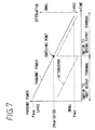
As shown in FIG. 7, when the attenuation ATT of the attenuator 1 is set to a minimum while the selective switch 2 is connected to the first output terminal 2, the transmit power (that is, a power level of the transmit signal supplied from the main transmission line A to the antenna) becomes a maximum level Pmax. On the contrary, when the attenuation ATT of the attenuator 1 is set to a maximum while the selective switch 2 is connected to the second output terminal 2 b, a total gain of the transmit power control circuit becomes minimum, and the transmit power becomes a minimum level Pmin.
When the transmit power is changed from the maximum level Pmax to a particular level (=Pmax−GA−CD), which is an attenuated maximum level attenuated by the sum of the gain GA of the amplifier 3 and the amount of coupling CD of the directional coupler 4, as shown by a right side of a mark “”, the attenuation ATT is changed with connecting the selective switch 2 to the first output terminal 2 a. In this case, the transmit power is changed in proportion to the attenuation ATT of the attenuator 1.
In a case where the attenuation ATT of the attenuator 1 is equal to the sum of the gain GA of the power amplifier 3 and the amount of coupling CD of the direction coupler 4 (in other words, when the gain of the attenuator 1 is reduced from the maximum gain Gmax (=0 dB) to a particular value, which is lower than the Gmax by the sum of the gain GA and the amount of coupling CD), the transmit power becomes Pmax−GA−CD. When the attenuation ATT is reduced from this condition, as shown by a left side of the mark “”, the transmit power Pmax can rise to the maximum level Pmax.
The operation described in the above will be described in detail by using specific values. For example, it assumes that the power level of the input signal inputted to the attenuator 1 is −10 dBm, the dynamic range of the attenuation ATT of the attenuator 1 is 0 dB-35 dB (in other words, the maximum gain Gmax is 0 dB, and the minimum gain Gmin is −35 dB), the gain GA of the amplifier 3 is 30 dB, and the amount of coupling CD of the directional coupler 4 is 5 dB. In this case, the maximum level Pmax of the transmit power is 20 dBm (=−10 dBm−0 dB+30 dB), and the minimum level Pmin is −50 dBm (=−10 dBm−35 dB−5 dB).
When the transmit power is changed from 20 dBm as the maximum level Pmax to −14 dBm (=Pmax−GA−CD−1 dB=20 dBm −30 dB −5 dB −1 dB), the attenuation ATT of the attenuator 1 is changed with selecting the selective switch 2 to the first output terminal 2 a. When the attenuation ATT becomes 35 dB (=GA+CD=30 dB+5 dB), the transmit power becomes −15 dBm. When it needs to further reduce the transmit power, the selective switch is switched to the second output terminal 2 b, the attenuation ATT is returned to 0 dB as the minimum value, and the attenuation ATT is changed in this condition. As a result, the transmit power can be changed from −15 dBm to −50 dBm as the minimum level Pmin.
On the contrary, when the transmit power is changed from −50 to −15 dBm, the attenuation ATT of the attenuator 1 is changed with selecting the selective switch 2 to the second output terminal 2 b. When the attenuation ATT becomes 0 dB as the minimum value, the transmit power becomes −15 dBm. When it needs to further reduce the transmit power, the selective switch is switched to the first output terminal 2 a, the attenuation ATT is set to 34 dB (=GA+CD−1 dB=30 dBm+5 dB−1 dB). As a result, the transmit power can be changed from −14 dBm to 20 dBm as the maximum level Pmax, when the attenuation ATT is changed in this condition.
The microcomputer 100 controls so that the transmit power accords with the target transmit output level, which indicates the power control signal from the base station. Therefore, when the microcomputer 100 compares the present transmit power and the target transmit output level, and determines that it needs to lower the transmit power, the microcomputer 100 increases the attenuation ATT of the attenuator 1 ΔA by ΔA (for example, ΔA=1 dB). When the attenuation ATT reaches 5 dB (=GA+CD), the selective switch 2 is switched to the second output terminal 2 b, and returns the attenuation ATT to 0 dB as the minimum value. After that, the microcomputer 100 increases the attenuation ATT from this condition ΔA by ΔA. On the contrary, when the microcomputer 100 determines that it needs to heighten the transmit power, the microcomputer 100 decreases the attenuation ATT of the attenuator 1 ΔA by ΔA. When the attenuation ATT reaches 0 dB as the minimum value, the selective switch 2 is switched to the first terminal 2 a, and returns the attenuation ATT to 5 dB. After that, the microcomputer 100 decreases the attenuation ATT from this condition ΔA by ΔA.
The above structure can control a transmit power of a transmit power control circuit through wide dynamic range.
Furthermore, according to the transmit power control circuit in the above, as shown in FIG. 6, when the selective switch 2 is switched to the second output terminal 2 b, the power supply transistor 8 is turned off, so that the power supply to the power amplifier 3 is cut off. As a result, the transmit power control circuit 3 can reduce power consumption. Furthermore, even if the radio-frequency signal leaks to former stage of the power amplifier 3, since the leaked signal is never amplified by the power amplifier 3, the microcomputer 100 can control the transmit power with a excellent linearity.
When the transmit power is detected to control the transmit power, it could be thought that a directional coupler 9 is provided at later stage of the directional coupler 9, so that one end is connected to the terminator 10 and another end is connected to the wave detector 11, as shown in FIG. 6.
Here, the detector 11 is constructed by a wave detection diode. The wave detection diode generally saturates when a range of input power is 30-40 dB. Therefore, when the transmit power is controlled through wide dynamic range over 70 dB, it would be difficult to obtain a dynamic range in accordance with the power range. Furthermore, it might be thought that an amount of coupling of the directional coupler 9 is increased in order to obtain wide power wave detection range; however, an insertion loss of the transmit power might increase in this case. Moreover, since two directional couplers are provided, the insertion loss might increase.
(First embodiment)
FIG. 1 shows a schematic block diagram of a transmit power control circuit of a first embodiment. In the drawings, same portions or corresponding portions as those in FIG. 6 are put the same numerals each other to eliminate redundant explanation.
In this embodiment, a direction coupler 12 is provided at latter stage of the power amplifier 3. One end of the direction coupler 12 is connected to a selective switch 13, and another end is connected to a selective switch 14. A first output terminal 13 a of the selective switch 13 is connected to a terminator 15, and a second output terminal 13 b is connected to the auxiliary transmission line B. A first output terminal 14 a of the selective switch 14 is connected to a wave detector (wave detection diode) 17, and a second output terminal 14 b is connected to a terminator 16.
The microcomputer 100 performs the substantially the same control as those of FIG. 6. In detail, the microcomputer 100 switches the switches 13 and 14 simultaneously with the switching of the selective switch 2. When the microcomputer 100 outputs the switching signal having a logically low level, the selective switches 2, 13 and 14 are respectively switched to the first output terminals 2 a, 13 a and 14 a. On the contrary, when the microcomputer 100 outputs the switching signal having a logically high level, the selective switches 2, 13 and 14 are respectively switched to the second output terminals 2 b, 13 b and 14 b.
Here, when the selective switches 2, 13 and 14 are switched to the first output terminals 2 a, 13 a and 14 a, the one end of the directional coupler 12 is connected to the terminator 13 and another end is connected to the wave detector 17. In this situation, similar to FIG. 6, the transmit power is controlled at the felt side of mark “” that is a range whose transmit power is relatively large. In this case, the microcomputer 100 controls the transmit power based on a detected output (detected voltage) from the wave detector 17.
On the contrary, when the selective switches 2, 13 and 14 are switched to the second output terminals 2 b, 13 b and 14 b, the one end of the directional coupler 12 is connected to the auxiliary transmission line B and another end is connected to the terminator 16. In this situation, similar to FIG. 6, the transmit power is controlled at the right side of mark “”, that is a range whose transmit power is relatively small. In this case, since the microcomputer 100 cannot detect the transmit power by using the wave detector 17, the microcomputer 100 controls the transmit power without using the output signal from the wave detector 17. In the radio communication using the CDMA method, an absolute transmit power accuracy range is wide and an absolute transmit power level accuracy is not required within a small transmit power range, it is no problem if the microcomputer 100 controls the transmit power without using the output signal from the wave detector 17.
According to this embodiment, one directional coupler 12 is used, and the transmit power is detected by using the wave detector 17 so that the transmit power is accurately controlled within a large transmit power range, and the transmit power is controlled by using the auxiliary transmission line B within a small transmit power range. As a result, since the transmit power control circuit does not use two directional couplers 4 and 9 as the transmit power control circuit shown in FIG. 6, the insertion loss can be reduced.
(Second embodiment)
According to the first embodiment, similar to the transmit power control circuit shown in FIG. 6, the attenuation of the attenuator 1 is switched at a timing when the selective switch 2 is switched to one of the first and second output terminal 2 a or 2 b.
In a wideband CDMA method, the transmit power control circuit performs a communication with a transmit data having a frame structure made up of a pilot symbol and data. When the transmit power overshoots or undershoots, since the transmit power widely varies, the transmit power control circuit might not accurately send the transmit data to the base station. In this case, since the transmit power control circuit using the wideband CDMA method synchronously communicates with the base station by using the pilot symbol, the transmit power control circuit might not accurately synchronously communicates with the base station when the pilot symbol is not adequately outputted. Furthermore, when the transmit power overshoots, the transmit power instantaneously rises. In such a case, the transmit power may be disturb radio wave for the base station.
In this third embodiment, as shown in FIG. 3, a second attenuator 20 is provided between the first output terminal 2 a of the selective switch 2 and the power amplifier 3, in addition to the attenuator 1 (in this embodiment, called as a first attenuator 1) which is provided at former stage of the selective switch 2. According to this structure, an attenuation of the second attenuator 20 is determined based on a control voltage, which is inputted from the microcomputer 100 via the D/A converter 21 and is amplified by the operational amplifier 22.
The microcomputer 100 of this embodiment controls the transmit power as follows.
When the microcomputer 100 decreases the transmit power from the maximum level, the selective switch 2 is switched to the first output terminal 2 a, so that the maximum value of an attenuation ATT1 of the first attenuator 1 is set to 0 dB. After that, the microcomputer 100 controls an attenuation ATT2 of the second attenuation 20 from the minimum value, 0 dB. As a result, the transmit power changes in accordance with the attenuation ATT2 of the second attenuator 20.
When the attenuation ATT2 of the second attenuator 20 reaches a sum of the gain GA of the power amplifier 3 and the amount of the coupler CD-1 of the directional coupler 34, the transmit power becomes Pmax-GA-CD-1. However, when the transmit power is further decreased, the selective switch 2 is switched to the second output terminal 2 b, and the attenuation ATT2 of the second attenuator 20 is kept to constant. In this situation, the microcomputer 100 controls so that the attenuation ATT1 of the first attenuator 1 becomes large. As a result, the transmit power can be further reduced to the minimum level in accordance with the attenuation ATT1 of the first attenuator 1.
On the contrary, while the selective switch 2 is switched to the second output terminal 2 b, when the transmit power is increased from the minimum level, the microcomputer 100 controls so that the attenuation ATT1 of the first attenuator 1 becomes small. When the attenuation ATT1 of the first attenuator 1 reaches t he minimum value, 0 dB, the selective switch 2 is switched to the first output terminal 2 a, and the attenuation ATT1 of the first attenuator 1 is kept to constant. In this situation, the microcomputer 100 controls so that the attenuation ATT2 of the second attenuator 20 becomes large.
According to this structure, the transmit power can be continuously changed between the maximum level and the minimum level. Furthermore, since the microcomputer 100 moves to a gain control by using one of the first and second attenuators 1 and 20, which has not been controlled until that time, with remaining the gain of another of the first and second attenuators 1 and 20, the microcomputer 100 can prevent the overshoot or the undershoot of the transmit power.
(Third embodiment)
In the second embodiment, the second attenuator 20 and the power amplifier 3 are applied. However, in a third embodiment, as shown in FIG. 4, a variable gain power amplifier 30, which amplifies by a positive gain based on the control signal as the input signal, may be used instead. In this case, the gain of the variable gain power amplifier 30 is controlled by the control voltage, which is inputted from the microcomputer 100 via the D/A converter 31 and is amplified by the operational amplifier 32.
The microcomputer 100 of this embodiment controls the transmit power as follows.
When the microcomputer 100 decreases the transmit power from the maximum level, the selective switch 2 is switched to the first output terminal 2 a, so that the maximum value of an attenuation ATT of the attenuator 1 is set to 0 dB. After that, the microcomputer 100 reduces a gain of the variable gain power amplifier 30 from the maximum value. As a result, the transmit power changes in accordance with the gain of the variable gain power amplifier 30.
When the gain of the variable gain power amplifier 30 reaches the minimum value, 0 dB, the selective switch 2 is switched to the second output terminal 2 b, and the gain of the variable gain power amplifier 30 is kept to constant. In this situation, the microcomputer 100 controls so that the attenuation ATT of the attenuator 1 becomes large. As a result, the transmit power can be further reduced to the minimum level in accordance with the attenuation ATT of the attenuator 1.
On the contrary, while the selective switch 2 is switched to the second output terminal 2 b, when the transmit power is increased from the minimum level, the microcomputer 100 controls so that the attenuation ATT of the attenuator 1 becomes small. When the attenuation ATT1 of the attenuator 1 reaches the minimum value, 0 dB, the selective switch 2 is switched to the first output terminal 2 a, and the attenuation ATT of the attenuator 1 is kept to constant. In this situation, the microcomputer 100 controls so that the gain of the variable gain power amplifier 30 becomes large.
According to this structure, the transmit power can be continuously changed between the maximum level and the minimum level. Furthermore, since the microcomputer 100 moves to a gain control by using one of the attenuators 1 and the variable gain power amplifier 30, which has not been controlled until that time, with remaining the gain of another of the attenuators 1 and the variable gain power amplifier 30, the microcomputer 100 can prevent the overshoot or the undershoot of the transmit power.
Here, in the third embodiment, the power amplifier 3 as shown described in the second embodiment can be connected to the variable gain power amplifier 30 in series. In the first to the third embodiments, the attenuator 1 is used for exemplifying the variable gain circuit, which is provided at the former stage of the selective switch 2. However, a variable amplifier, which amplifies by a positive gain in accordance with a control as an input signal, or a variable amplifier, which amplifies by one of a positive and a negative gain. Furthermore, the transmit power control circuit 3 can be applied to the other radio communication apparatus than the portable telephone.

Claims (8)

What is claimed is:
1. A transmit power control circuit comprising:
a variable gain circuit for inputting a radio-frequency signal, for amplifying the radio-frequency signal with a gain which changing based on an external control signal, and for outputting an amplified radio-frequency signal as an output signal;
a first switching circuit for selecting one of a main transmission line and an auxiliary transmission line, and for outputting the output signal of the variable gain circuit to the one of the main transmission line and the auxiliary transmission line;
an amplifying circuit provided to the main transmission line, and for amplifying the output signal of the variable gain circuit, which being outputted to the main transmission line;
a directional coupler coupled with the main transmission line with a predetermined amount of coupling, and having one end and another end;
a second switching circuit for connecting the one end of the directional coupler to a first terminator when the output signal of the variable gain circuit is outputted to the main transmission line, and for connecting the one end of the directional coupler to the auxiliary transmission line when the output signal of the variable gain circuit is outputted to the auxiliary transmission line; and
a third switching circuit for connecting said another end of the directional coupler to a wave detector when the output signal of the variable gain circuit is outputted to the main transmission line, and for connecting said another end of the directional coupler to a second terminator when the output signal of the variable gain circuit is outputted to the auxiliary transmission line.
2. The circuit according to claim 1, wherein the amplifying circuit includes an amplifier for amplifying by using a predetermined positive gain.
3. The circuit according to claim 2, further comprising a power shutdown circuit for shutting down off a power supply to the amplifier, when the first switching circuit switches the selection from the main transmission line to the auxiliary transmission line.
4. The circuit according to claim 1, wherein:
the amplifying circuit includes an attenuator for amplifying the output signal of the variable gain circuit based on an another control signal, and
an attenuation of the attenuator is controlled without changing a gain of the variable gain circuit when the output signal of the variable gain circuit is outputted to the main transmission line, and the attenuation of the variable gain circuit is controlled without changing the gain of the attenuator when the output signal of the variable gain circuit is outputted to the auxiliary transmission line.
5. The circuit according to claim 1, wherein:
the amplifying circuit includes a variable gain power amplifier whose gain changes based on the external control signal,
a gain of the variable gain power amplifier is controlled without changing a gain of the variable gain circuit when the output signal of the variable gain circuit is outputted to the main transmission line, and
the gain of the variable gain circuit is controlled without changing the gain of the variable gain power amplifier when the output signal of the variable gain circuit is outputted to the auxiliary transmission line.
6. A transmit power control circuit comprising:
a variable gain circuit for inputting a radio-frequency signal, for amplifying the radio-frequency signal with a gain which changing based on an external control signal, and for outputting an amplified radio-frequency signal as an output signal;
a first switching circuit for selecting one of a main transmission line and an auxiliary transmission line, and for outputting the output signal of the variable gain circuit to the one of the main transmission line and the auxiliary transmission line;
an amplifying circuit provided to the main transmission line, and for amplifying the output signal of the variable gain circuit, which being outputted to the main transmission line; and
a directional coupler coupled with the main transmission line with a predetermined amount of coupling, and having one end and another end; and
a second switching circuit for connecting the one end of the directional coupler to a first terminator when the output signal of the variable gain circuit is outputted to the main transmission line, and for connecting the one end of the directional coupler to the auxiliary transmission line when the output signal of the variable gain circuit is outputted to the auxiliary transmission line.
7. A transmit power control circuit comprising:
a variable gain circuit for inputting a radio-frequency signal, for amplifying the radio-frequency signal with a gain which changing based on an external control signal, and for outputting an amplified radio-frequency signal as an output signal;
a first switching circuit for selecting one of a main transmission line and an auxiliary transmission line, and for outputting the output signal of the variable gain circuit to the one of the main transmission line and the auxiliary transmission line;
an amplifying circuit provided to the main transmission line, and for amplifying the output signal of the variable gain circuit, which being outputted to the main transmission line;
a directional coupler coupled with the main transmission line with a predetermined amount of coupling, and having one end and another end; and
a second switching circuit for connecting said another end of the directional coupler to a wave detector when the output signal of the variable gain circuit is outputted to the main transmission line, and for connecting said another end of the directional coupler to a second terminator when the output signal of the variable gain circuit is outputted to the auxiliary transmission line.
8. A transmit power control circuit comprising:
a variable gain circuit for inputting a radio-frequency signal, for amplifying the radio-frequency signal with a gain which changing based on an external control signal, and for outputting an amplified radio-frequency signal as an output signal;
a first switching circuit for selecting one of a main transmission line and an auxiliary transmission line, and for outputting the output signal of the variable gain circuit to the one of the main transmission line and the auxiliary transmission line;
an amplifying circuit provided to the main transmission line, and for amplifying the output signal of the variable gain circuit, which being outputted to the main transmission line; and
a directional coupler coupled with the main transmission line with a predetermined amount of coupling, and having one end and another end,
wherein the one end of the directional coupler is electrically connected to an auxiliary transmission line, and said another end of the directional coupler is electrically connected to a terminator.
US09/561,781 1999-05-13 2000-05-01 Transmit power control circuit Expired - Lifetime US6498925B1 (en)

Applications Claiming Priority (2)

Application Number Priority Date Filing Date Title
JP13316599A JP4062816B2 (en) 1999-05-13 1999-05-13 Transmission power control circuit
JP11-133165 1999-05-13

Publications (1)

Publication Number Publication Date
US6498925B1 true US6498925B1 (en) 2002-12-24

Family

ID=15098215

Family Applications (1)

Application Number Title Priority Date Filing Date
US09/561,781 Expired - Lifetime US6498925B1 (en) 1999-05-13 2000-05-01 Transmit power control circuit

Country Status (3)

Country Link
US (1) US6498925B1 (en)
JP (1) JP4062816B2 (en)
DE (1) DE10023460B4 (en)

Cited By (46)

* Cited by examiner, † Cited by third party
Publication number Priority date Publication date Assignee Title
US20020154708A1 (en) * 2001-03-08 2002-10-24 Siemens Information And Communication Mobile Llc Automatic transmit power control loop with modulation averaging
US20030017813A1 (en) * 2001-07-17 2003-01-23 Satoshi Maruyama Parallel operation system of transmission amplifier
US20040219944A1 (en) * 2000-10-23 2004-11-04 Ilan Barak Automatic level control
US6856812B1 (en) * 2000-06-30 2005-02-15 Lucent Technologies Inc. Downlink power control method for wireless packet data network
US20070171997A1 (en) * 2005-08-25 2007-07-26 Haim Weissman Method and apparatus for control of transmitter power consumption
US20080205317A1 (en) * 2005-03-04 2008-08-28 Antti Piipponen Link Establishment in a Wireless Communication Environment
US20090265745A1 (en) * 2008-04-17 2009-10-22 Egan Jr John M Reversible Faceplate Terminal Adapter Which Changes Signal Flow Direction
US20100100918A1 (en) * 2008-10-21 2010-04-22 Egan Jr John M Multi-Port Entry Adapter, Hub and Method for Interfacing a CATV Network and a MoCA Network
US20100100922A1 (en) * 2008-10-16 2010-04-22 John Mezzalingua Associates, Inc. Downstream output level and/or output level tilt compensation device between catv distribution system and catv user
US20100100921A1 (en) * 2008-10-16 2010-04-22 John Mezzalingua Associates, Inc. Dynamically configurable frequency band selection device between catv distribution system and catv user
US20100125877A1 (en) * 2008-10-21 2010-05-20 Wells Chad T CATV Entry Adapter and Method for Preventing Interference with eMTA Equipment from MoCA Signals
US20100146564A1 (en) * 2008-10-21 2010-06-10 Halik Gregory F CATV Entry Adapter and Method Utilizing Directional Couplers for MoCA Signal Communication
US20100251322A1 (en) * 2009-03-30 2010-09-30 Raymond Palinkas Upstream bandwidth conditioning device
US20100251321A1 (en) * 2009-03-30 2010-09-30 Raymond Palinkas Upstream bandwidth conditioning device
US20100251323A1 (en) * 2009-03-30 2010-09-30 Jackson David H Upstream bandwidth conditioning device
US20100251314A1 (en) * 2009-03-30 2010-09-30 John Mezzalingua Associates, Inc. Total bandwidth conditioning device
US20100244980A1 (en) * 2009-03-30 2010-09-30 Olson Thomas A Method and apparatus for a self-terminating signal path
US20100279630A1 (en) * 2009-04-29 2010-11-04 Lockheed Martin Corporation Radio frequency power monitor
US20100301972A1 (en) * 2009-05-29 2010-12-02 John Mezzalingua Associates, Inc. Self-terminating coaxial cable port
US20110072472A1 (en) * 2009-09-21 2011-03-24 Wells Chad T Passive Multi-Port Entry Adapter and Method for Preserving Downstream CATV Signal Strength within In-Home Network
US20110085045A1 (en) * 2009-10-09 2011-04-14 John Mezzalingua Associates, Inc. Modulation analyzer and level measurement device
US20110085480A1 (en) * 2009-10-09 2011-04-14 John Mezzalingua Associates, Inc. Upstream bandwidth conditioning device
US20110085452A1 (en) * 2009-10-09 2011-04-14 John Mezzalingua Associates, Inc. Upstream bandwidth level measurement device
US20110085586A1 (en) * 2009-10-09 2011-04-14 John Mezzalingua Associates, Inc. Total bandwidth conditioning device
US20110088077A1 (en) * 2009-10-09 2011-04-14 John Mezzalingua Associates, Inc. Downstream bandwidth conditioning device
US20110181371A1 (en) * 2010-01-26 2011-07-28 John Mezzalingua Associates, Inc. Band selective isolation bridge for splitter
US20110187481A1 (en) * 2010-02-01 2011-08-04 John Mezzalingua Associates, Inc. Multipath mitigation circuit for home network
US8141122B2 (en) 2009-03-30 2012-03-20 John Mezzalingua Associates, Inc. RF terminate/permit system
US8179814B2 (en) 2009-03-30 2012-05-15 John Mezzalingua Associates, Inc. Automatic return path switching for a signal conditioning device
US20130113560A1 (en) * 2011-11-09 2013-05-09 Murata Manufacturing Co., Ltd. Power amplifying circuit and high-frequency module
US8464301B2 (en) 2008-10-16 2013-06-11 Ppc Broadband, Inc. Upstream bandwidth conditioning device between CATV distribution system and CATV user
US8479247B2 (en) 2010-04-14 2013-07-02 Ppc Broadband, Inc. Upstream bandwidth conditioning device
US8561125B2 (en) 2010-08-30 2013-10-15 Ppc Broadband, Inc. Home network frequency conditioning device and method
JP2016025542A (en) * 2014-07-23 2016-02-08 富士電機株式会社 Wireless communication device
US9264012B2 (en) 2012-06-25 2016-02-16 Ppc Broadband, Inc. Radio frequency signal splitter
US20160079649A1 (en) * 2014-09-12 2016-03-17 Infineon Technologies Ag System and Method for a Directional Coupler Module
US9351051B2 (en) 2008-10-13 2016-05-24 Ppc Broadband, Inc. CATV entry adapter and method for distributing CATV and in-home entertainment signals
US9363469B2 (en) 2008-07-17 2016-06-07 Ppc Broadband, Inc. Passive-active terminal adapter and method having automatic return loss control
US9647851B2 (en) 2008-10-13 2017-05-09 Ppc Broadband, Inc. Ingress noise inhibiting network interface device and method for cable television networks
US10021343B2 (en) 2010-12-21 2018-07-10 Ppc Broadband, Inc. Method and apparatus for reducing isolation in a home network
US10142677B2 (en) 2008-10-21 2018-11-27 Ppc Broadband, Inc. Entry device for a CATV network
US10177445B1 (en) * 2017-07-05 2019-01-08 National Chung Shan Institute Of Science And Technology Communication structure
US10212392B2 (en) 2016-06-30 2019-02-19 Ppc Broadband, Inc. Passive enhanced MoCA entry device
TWI720309B (en) * 2015-02-15 2021-03-01 美商西凱渥資訊處理科技公司 Unpowered switching module
US11076191B2 (en) 2018-01-19 2021-07-27 Ppc Broadband, Inc. Systems and methods for extending an in-home splitter network
US11910052B2 (en) 2008-10-21 2024-02-20 Ppc Broadband, Inc. Entry device for communicating external network signals and in-home network signals

Families Citing this family (1)

* Cited by examiner, † Cited by third party
Publication number Priority date Publication date Assignee Title
DE10150476A1 (en) * 2001-10-16 2003-04-17 Thomson Brandt Gmbh Reducing transmitter power losses when operating bi-directional communications system with wireless data signal transmission involves evaluating transmission, adapting supply energy

Citations (12)

* Cited by examiner, † Cited by third party
Publication number Priority date Publication date Assignee Title
US5023937A (en) * 1989-05-09 1991-06-11 Motorola, Inc. Transmitter with improved linear amplifier control
US5196806A (en) * 1990-10-19 1993-03-23 Nec Corporation Output level control circuit for use in rf power amplifier
US5530923A (en) * 1994-03-30 1996-06-25 Nokia Mobile Phones Ltd. Dual mode transmission system with switched linear amplifier
US5697074A (en) * 1995-03-30 1997-12-09 Nokia Mobile Phones Limited Dual rate power control loop for a transmitter
JPH10150429A (en) 1996-11-18 1998-06-02 Matsushita Electric Ind Co Ltd Transmission circuit
US6038432A (en) * 1997-10-07 2000-03-14 Fujitsu Limited Automatic transmission power control circuit
US6108527A (en) * 1997-07-31 2000-08-22 Lucent Technologies, Inc. Wide range multiple band RF power detector
US6151509A (en) * 1998-06-24 2000-11-21 Conexant Systems, Inc. Dual band cellular phone with two power amplifiers and a current detector for monitoring the consumed power
US6178309B1 (en) * 1996-09-17 2001-01-23 Nec Corporation Electronic device having an AGC loop
US6215987B1 (en) * 1997-06-06 2001-04-10 Nec Corporation Mobile communication transmitter capable of selectively activating amplifiers
US6288606B1 (en) * 1998-11-10 2001-09-11 Nokia Mobile Phones Ltd. Linear power amplifier arrangement and method for its operation
US6301486B1 (en) * 1998-04-03 2001-10-09 Nec Corporation Radio telephone apparatus

Family Cites Families (1)

* Cited by examiner, † Cited by third party
Publication number Priority date Publication date Assignee Title
US5898338A (en) * 1996-09-20 1999-04-27 Spectrian Adaptive digital predistortion linearization and feed-forward correction of RF power amplifier

Patent Citations (12)

* Cited by examiner, † Cited by third party
Publication number Priority date Publication date Assignee Title
US5023937A (en) * 1989-05-09 1991-06-11 Motorola, Inc. Transmitter with improved linear amplifier control
US5196806A (en) * 1990-10-19 1993-03-23 Nec Corporation Output level control circuit for use in rf power amplifier
US5530923A (en) * 1994-03-30 1996-06-25 Nokia Mobile Phones Ltd. Dual mode transmission system with switched linear amplifier
US5697074A (en) * 1995-03-30 1997-12-09 Nokia Mobile Phones Limited Dual rate power control loop for a transmitter
US6178309B1 (en) * 1996-09-17 2001-01-23 Nec Corporation Electronic device having an AGC loop
JPH10150429A (en) 1996-11-18 1998-06-02 Matsushita Electric Ind Co Ltd Transmission circuit
US6215987B1 (en) * 1997-06-06 2001-04-10 Nec Corporation Mobile communication transmitter capable of selectively activating amplifiers
US6108527A (en) * 1997-07-31 2000-08-22 Lucent Technologies, Inc. Wide range multiple band RF power detector
US6038432A (en) * 1997-10-07 2000-03-14 Fujitsu Limited Automatic transmission power control circuit
US6301486B1 (en) * 1998-04-03 2001-10-09 Nec Corporation Radio telephone apparatus
US6151509A (en) * 1998-06-24 2000-11-21 Conexant Systems, Inc. Dual band cellular phone with two power amplifiers and a current detector for monitoring the consumed power
US6288606B1 (en) * 1998-11-10 2001-09-11 Nokia Mobile Phones Ltd. Linear power amplifier arrangement and method for its operation

Cited By (106)

* Cited by examiner, † Cited by third party
Publication number Priority date Publication date Assignee Title
US6856812B1 (en) * 2000-06-30 2005-02-15 Lucent Technologies Inc. Downlink power control method for wireless packet data network
US7471935B2 (en) * 2000-10-23 2008-12-30 Intel Corporation Automatic level control
US20040219944A1 (en) * 2000-10-23 2004-11-04 Ilan Barak Automatic level control
US20020154708A1 (en) * 2001-03-08 2002-10-24 Siemens Information And Communication Mobile Llc Automatic transmit power control loop with modulation averaging
US7570709B2 (en) * 2001-03-08 2009-08-04 Siemens Aktiengesellschaft Automatic transmit power control loop with modulation averaging
US7254377B2 (en) * 2001-07-17 2007-08-07 Fujitsu Limited Parallel operation system of transmission amplifier
US20030017813A1 (en) * 2001-07-17 2003-01-23 Satoshi Maruyama Parallel operation system of transmission amplifier
US20080205317A1 (en) * 2005-03-04 2008-08-28 Antti Piipponen Link Establishment in a Wireless Communication Environment
US8711816B2 (en) 2005-03-04 2014-04-29 Nokia Corporation Link establishment in a wireless communication environment
US7711070B2 (en) * 2005-08-25 2010-05-04 Qualcomm, Incorporated Method and apparatus for control of transmitter power consumption
US20070171997A1 (en) * 2005-08-25 2007-07-26 Haim Weissman Method and apparatus for control of transmitter power consumption
US20090265745A1 (en) * 2008-04-17 2009-10-22 Egan Jr John M Reversible Faceplate Terminal Adapter Which Changes Signal Flow Direction
US10257462B2 (en) 2008-07-17 2019-04-09 Ppc Broadband, Inc. Adapter for a cable-television network
US9769418B2 (en) 2008-07-17 2017-09-19 Ppc Broadband, Inc. Passive-active terminal adapter and method having automatic return loss control
US9363469B2 (en) 2008-07-17 2016-06-07 Ppc Broadband, Inc. Passive-active terminal adapter and method having automatic return loss control
US9647851B2 (en) 2008-10-13 2017-05-09 Ppc Broadband, Inc. Ingress noise inhibiting network interface device and method for cable television networks
US10154302B2 (en) 2008-10-13 2018-12-11 Ppc Broadband, Inc. CATV entry adapter and method for distributing CATV and in-home entertainment signals
US10187673B2 (en) 2008-10-13 2019-01-22 Ppc Broadband, Inc. Ingress noise inhibiting network interface device and method for cable television networks
US10045056B2 (en) 2008-10-13 2018-08-07 Ppc Broadband, Inc. Ingress noise inhibiting network interface device and method for cable television networks
US9781472B2 (en) 2008-10-13 2017-10-03 Ppc Broadband, Inc. CATV entry adapter and method for distributing CATV and in-home entertainment signals
US9351051B2 (en) 2008-10-13 2016-05-24 Ppc Broadband, Inc. CATV entry adapter and method for distributing CATV and in-home entertainment signals
US8464301B2 (en) 2008-10-16 2013-06-11 Ppc Broadband, Inc. Upstream bandwidth conditioning device between CATV distribution system and CATV user
US10924811B2 (en) 2008-10-16 2021-02-16 Ppc Broadband, Inc. Compensation device for maintaining a desired signal quality in transmitted signals
US9271026B2 (en) 2008-10-16 2016-02-23 Ppc Broadband, Inc. Dynamically configurable frequency band selection device between CATV distribution system and CATV user
US8832767B2 (en) 2008-10-16 2014-09-09 Ppc Broadband, Inc. Dynamically configurable frequency band selection device between CATV distribution system and CATV user
US10264325B2 (en) 2008-10-16 2019-04-16 Ppc Broadband, Inc. System, method and device having teaching and commerce subsystems
US20100100921A1 (en) * 2008-10-16 2010-04-22 John Mezzalingua Associates, Inc. Dynamically configurable frequency band selection device between catv distribution system and catv user
US20100100922A1 (en) * 2008-10-16 2010-04-22 John Mezzalingua Associates, Inc. Downstream output level and/or output level tilt compensation device between catv distribution system and catv user
US8001579B2 (en) 2008-10-16 2011-08-16 John Mezzalingua Associates, Inc. Downstream output level and/or output level tilt compensation device between CATV distribution system and CATV user
US10341718B2 (en) 2008-10-21 2019-07-02 Ppc Broadband, Inc. Passive multi-port entry adapter and method for preserving downstream CATV signal strength within in-home network
US10154304B2 (en) 2008-10-21 2018-12-11 Ppc Broadband, Inc. Methods for controlling CATV signal communication between a CATV network and an in-home network, and preserving downstream CATV signal strength within the in-home network
US10154303B2 (en) 2008-10-21 2018-12-11 Ppc Broadband, Inc. Entry adapter that blocks different frequency bands and preserves downstream signal strength
US10149004B2 (en) 2008-10-21 2018-12-04 Ppc Broadband, Inc. Entry device and method for communicating CATV signals and MoCA in-home network signals in an entry device
US10142677B2 (en) 2008-10-21 2018-11-27 Ppc Broadband, Inc. Entry device for a CATV network
US10284904B2 (en) 2008-10-21 2019-05-07 Ppc Broadband, Inc. Entry adapters for conducting can signals and in-home network signals
US10284903B2 (en) 2008-10-21 2019-05-07 Ppc Broadband, Inc. Entry adapters for frequency band blocking internal network signals
US8510782B2 (en) 2008-10-21 2013-08-13 Ppc Broadband, Inc. CATV entry adapter and method for preventing interference with eMTA equipment from MoCA Signals
US10341719B2 (en) 2008-10-21 2019-07-02 Ppc Broadband, Inc. Entry adapter for communicating external signals to an internal network and communicating client signals in the client network
US10419813B2 (en) 2008-10-21 2019-09-17 Ppc Broadband, Inc. Passive multi-port entry adapter for preserving downstream CATV signal strength
US10917685B2 (en) 2008-10-21 2021-02-09 Ppc Broadband, Inc. Entry device for communicating signals between an external network and an in-home network
US8286209B2 (en) 2008-10-21 2012-10-09 John Mezzalingua Associates, Inc. Multi-port entry adapter, hub and method for interfacing a CATV network and a MoCA network
US11528526B2 (en) 2008-10-21 2022-12-13 Ppc Broadband, Inc. Entry device for communicating external network signals and in-home network signals
US11910052B2 (en) 2008-10-21 2024-02-20 Ppc Broadband, Inc. Entry device for communicating external network signals and in-home network signals
US20100146564A1 (en) * 2008-10-21 2010-06-10 Halik Gregory F CATV Entry Adapter and Method Utilizing Directional Couplers for MoCA Signal Communication
US8429695B2 (en) 2008-10-21 2013-04-23 Ppc Broadband, Inc. CATV entry adapter and method utilizing directional couplers for MoCA signal communication
US20100125877A1 (en) * 2008-10-21 2010-05-20 Wells Chad T CATV Entry Adapter and Method for Preventing Interference with eMTA Equipment from MoCA Signals
US20100100918A1 (en) * 2008-10-21 2010-04-22 Egan Jr John M Multi-Port Entry Adapter, Hub and Method for Interfacing a CATV Network and a MoCA Network
US8584192B2 (en) 2009-03-30 2013-11-12 Ppc Broadband, Inc. Upstream bandwidth conditioning device
US8179814B2 (en) 2009-03-30 2012-05-15 John Mezzalingua Associates, Inc. Automatic return path switching for a signal conditioning device
US20100251322A1 (en) * 2009-03-30 2010-09-30 Raymond Palinkas Upstream bandwidth conditioning device
US20100251321A1 (en) * 2009-03-30 2010-09-30 Raymond Palinkas Upstream bandwidth conditioning device
US20100251323A1 (en) * 2009-03-30 2010-09-30 Jackson David H Upstream bandwidth conditioning device
US20100251314A1 (en) * 2009-03-30 2010-09-30 John Mezzalingua Associates, Inc. Total bandwidth conditioning device
US20100244980A1 (en) * 2009-03-30 2010-09-30 Olson Thomas A Method and apparatus for a self-terminating signal path
US8990881B2 (en) 2009-03-30 2015-03-24 Ppc Broadband, Inc. Upstream bandwidth conditioning device
US8082570B2 (en) 2009-03-30 2011-12-20 John Mezzalingua Associates, Inc. Method and apparatus for a self-terminating signal path
US8141122B2 (en) 2009-03-30 2012-03-20 John Mezzalingua Associates, Inc. RF terminate/permit system
US8181211B2 (en) 2009-03-30 2012-05-15 John Mezzalingua Associates, Inc. Total bandwidth conditioning device
US20100279630A1 (en) * 2009-04-29 2010-11-04 Lockheed Martin Corporation Radio frequency power monitor
US8027648B2 (en) * 2009-04-29 2011-09-27 Lockheed Martin Corporation Radio frequency power monitor
US20100301972A1 (en) * 2009-05-29 2010-12-02 John Mezzalingua Associates, Inc. Self-terminating coaxial cable port
US8098113B2 (en) 2009-05-29 2012-01-17 John Mezzalingua Associates, Inc. Self-terminating coaxial cable port
US9860591B2 (en) 2009-09-21 2018-01-02 Ppc Broadband, Inc. Passive multi-port entry adapter and method for preserving downstream CATV signal strength within in-home network
US20110072472A1 (en) * 2009-09-21 2011-03-24 Wells Chad T Passive Multi-Port Entry Adapter and Method for Preserving Downstream CATV Signal Strength within In-Home Network
US8356322B2 (en) 2009-09-21 2013-01-15 John Mezzalingua Associates, Inc. Passive multi-port entry adapter and method for preserving downstream CATV signal strength within in-home network
US9516376B2 (en) 2009-09-21 2016-12-06 Ppc Broadband, Inc. Passive multi-port entry adapter and method for preserving downstream CATV signal strength within in-home network
US9167286B2 (en) 2009-09-21 2015-10-20 Ppc Broadband, Inc. Passive multi-port entry adapter and method for preserving downstream CATV signal strength within in-home network
US20110085586A1 (en) * 2009-10-09 2011-04-14 John Mezzalingua Associates, Inc. Total bandwidth conditioning device
US8516537B2 (en) 2009-10-09 2013-08-20 Ppc Broadband, Inc. Downstream bandwidth conditioning device
US8274566B2 (en) 2009-10-09 2012-09-25 John Mezzalingua Associates, Inc. Modulation analyzer and level measurement device
US20110085452A1 (en) * 2009-10-09 2011-04-14 John Mezzalingua Associates, Inc. Upstream bandwidth level measurement device
US20110088077A1 (en) * 2009-10-09 2011-04-14 John Mezzalingua Associates, Inc. Downstream bandwidth conditioning device
US20110085045A1 (en) * 2009-10-09 2011-04-14 John Mezzalingua Associates, Inc. Modulation analyzer and level measurement device
US8213457B2 (en) 2009-10-09 2012-07-03 John Mezzalingua Associates, Inc. Upstream bandwidth conditioning device
US8385219B2 (en) 2009-10-09 2013-02-26 John Mezzalingua Associates, Inc. Upstream bandwidth level measurement device
US20110085480A1 (en) * 2009-10-09 2011-04-14 John Mezzalingua Associates, Inc. Upstream bandwidth conditioning device
US20110181371A1 (en) * 2010-01-26 2011-07-28 John Mezzalingua Associates, Inc. Band selective isolation bridge for splitter
US8350641B2 (en) 2010-01-26 2013-01-08 John Mezzalingua Associates, Inc. Band selective isolation bridge for splitter
US9979373B2 (en) 2010-02-01 2018-05-22 Ppc Broadband, Inc. Multipath mitigation circuit for home network
US20110187481A1 (en) * 2010-02-01 2011-08-04 John Mezzalingua Associates, Inc. Multipath mitigation circuit for home network
US10790793B2 (en) 2010-02-01 2020-09-29 Ppc Broadband, Inc. Filter circuit
US8487717B2 (en) 2010-02-01 2013-07-16 Ppc Broadband, Inc. Multipath mitigation circuit for home network
US10284162B2 (en) 2010-02-01 2019-05-07 Ppc Broadband, Inc. Multipath mitigation circuit for home network
US11444592B2 (en) 2010-02-01 2022-09-13 Ppc Broadband, Inc. Filter circuit
US9306530B2 (en) 2010-02-01 2016-04-05 Ppc Broadband, Inc. Multipath mitigation circuit for home network
US8479247B2 (en) 2010-04-14 2013-07-02 Ppc Broadband, Inc. Upstream bandwidth conditioning device
US8561125B2 (en) 2010-08-30 2013-10-15 Ppc Broadband, Inc. Home network frequency conditioning device and method
US10750120B2 (en) 2010-12-21 2020-08-18 Ppc Broadband, Inc. Method and apparatus for reducing isolation in a home network
US10021343B2 (en) 2010-12-21 2018-07-10 Ppc Broadband, Inc. Method and apparatus for reducing isolation in a home network
US11070766B2 (en) 2010-12-21 2021-07-20 Ppc Broadband, Inc. Method and apparatus for reducing isolation in a home network
US20130113560A1 (en) * 2011-11-09 2013-05-09 Murata Manufacturing Co., Ltd. Power amplifying circuit and high-frequency module
US8797102B2 (en) * 2011-11-09 2014-08-05 Murata Manufacturing Co., Ltd. Power amplifying circuit and high-frequency module
US9641147B2 (en) 2012-06-25 2017-05-02 Ppc Broadband, Inc. Radio frequency signal splitter
US9264012B2 (en) 2012-06-25 2016-02-16 Ppc Broadband, Inc. Radio frequency signal splitter
US9929457B2 (en) 2012-06-25 2018-03-27 Ppc Broadband, Inc. Radio frequency signal splitter
JP2016025542A (en) * 2014-07-23 2016-02-08 富士電機株式会社 Wireless communication device
US9866260B2 (en) * 2014-09-12 2018-01-09 Infineon Technologies Ag System and method for a directional coupler module
US20160079649A1 (en) * 2014-09-12 2016-03-17 Infineon Technologies Ag System and Method for a Directional Coupler Module
TWI720309B (en) * 2015-02-15 2021-03-01 美商西凱渥資訊處理科技公司 Unpowered switching module
US10212392B2 (en) 2016-06-30 2019-02-19 Ppc Broadband, Inc. Passive enhanced MoCA entry device
US11076129B2 (en) 2016-06-30 2021-07-27 Ppc Broadband, Inc. MoCA entry device
US10582160B2 (en) 2016-06-30 2020-03-03 Ppc Broadband, Inc. MoCA entry device
US11647162B2 (en) 2016-06-30 2023-05-09 Ppc Broadband, Inc. MoCA entry device
US20190013567A1 (en) * 2017-07-05 2019-01-10 National Chung Shan Institute Of Science And Technology Communication structure
US10177445B1 (en) * 2017-07-05 2019-01-08 National Chung Shan Institute Of Science And Technology Communication structure
US11076191B2 (en) 2018-01-19 2021-07-27 Ppc Broadband, Inc. Systems and methods for extending an in-home splitter network

Also Published As

Publication number Publication date
JP4062816B2 (en) 2008-03-19
JP2000323998A (en) 2000-11-24
DE10023460A1 (en) 2000-11-16
DE10023460B4 (en) 2014-01-09

Similar Documents

Publication Publication Date Title
US6498925B1 (en) Transmit power control circuit
KR100241780B1 (en) Power saving apparatus for radio communication terminal
US6807403B2 (en) Radio telephone apparatus
US5303395A (en) Power control with a constant gain amplifier for portable radio transceivers
US5126688A (en) Power amplifying apparatus for wireless transmitter
US5291147A (en) Power booster for a radio telephone
US5182527A (en) Power amplifying apparatus for wireless transmitter
US5442322A (en) Power amplifier bias control circuit and method
US5884149A (en) Mobile station having dual band RF detector and gain control
US6463264B1 (en) Wireless communication apparatus and transmission power control method in wireless communication apparatus
US5392464A (en) Directional detector for power level control
CN100356701C (en) Transmission power control device and method thereof, computer program for transmission power control device, and radio transmitter
US20040174218A1 (en) Method and apparatus for controlling the output power of a power amplifier
KR20020015946A (en) Matching apparatus
US6486738B2 (en) Device for controlling power in power amplifier of a portable wireless terminal
EP0560548A1 (en) Power control circuit
US6526266B1 (en) Transmission electric power control device and control method
GB2282502A (en) Correction for non-linearity in an amplifier output detector in a feedback loop
KR100442608B1 (en) Apparatus and method for keeping linearity of radio frequency receiver block in mobile communication system
US7123932B2 (en) Apparatus for stabilizing transmission power of broadband code division multiple access type mobile communication terminal
CN211352183U (en) Feedback receiver circuit and electronic equipment
KR100377083B1 (en) Power control circuit
KR20070023263A (en) Apparatus For Controlling Power Amplifier Input Level In The Mobile Communication Terminal
KR20000043152A (en) Circuit for limiting output level of high frequency system
JP2000252843A (en) Transmission power control circuit

Legal Events

Date Code Title Description
AS Assignment

Owner name: IPICS CORPORATION, JAPAN

Free format text: ASSIGNMENT OF ASSIGNORS INTEREST;ASSIGNOR:TAUCHI, NOBUTAKA;REEL/FRAME:010789/0672

Effective date: 20000424

AS Assignment

Owner name: DENSO CORPORATION, JAPAN

Free format text: CORRECTIVE ASSIGNMENT TO CORRECT THE NAME OF THE ASSIGNEE, FILED ON 05-01-00, RECORDED ON REEL 10789 FRAME 0672;ASSIGNOR:TAUCHI, NOBUTAKA;REEL/FRAME:010845/0216

Effective date: 20000420

STCF Information on status: patent grant

Free format text: PATENTED CASE

FPAY Fee payment

Year of fee payment: 4

FPAY Fee payment

Year of fee payment: 8

FEPP Fee payment procedure

Free format text: PAYOR NUMBER ASSIGNED (ORIGINAL EVENT CODE: ASPN); ENTITY STATUS OF PATENT OWNER: LARGE ENTITY

FPAY Fee payment

Year of fee payment: 12