US6512694B2 - NAND stack EEPROM with random programming capability - Google Patents
NAND stack EEPROM with random programming capability Download PDFInfo
- Publication number
- US6512694B2 US6512694B2 US09/681,314 US68131401A US6512694B2 US 6512694 B2 US6512694 B2 US 6512694B2 US 68131401 A US68131401 A US 68131401A US 6512694 B2 US6512694 B2 US 6512694B2
- Authority
- US
- United States
- Prior art keywords
- volatile memory
- memory cells
- series
- controller
- connected non
- Prior art date
- Legal status (The legal status is an assumption and is not a legal conclusion. Google has not performed a legal analysis and makes no representation as to the accuracy of the status listed.)
- Expired - Lifetime
Links
Images


Classifications
-
- G—PHYSICS
- G11—INFORMATION STORAGE
- G11C—STATIC STORES
- G11C16/00—Erasable programmable read-only memories
- G11C16/02—Erasable programmable read-only memories electrically programmable
- G11C16/06—Auxiliary circuits, e.g. for writing into memory
- G11C16/10—Programming or data input circuits
-
- G—PHYSICS
- G11—INFORMATION STORAGE
- G11C—STATIC STORES
- G11C16/00—Erasable programmable read-only memories
- G11C16/02—Erasable programmable read-only memories electrically programmable
- G11C16/04—Erasable programmable read-only memories electrically programmable using variable threshold transistors, e.g. FAMOS
- G11C16/0483—Erasable programmable read-only memories electrically programmable using variable threshold transistors, e.g. FAMOS comprising cells having several storage transistors connected in series
Definitions
- the present invention relates to a electrically erasable programmable read-only memory (EEPROM) and, more specifically, to a NAND stack EEPROM.
- EEPROM electrically erasable programmable read-only memory
- a computer system is comprised of a memory for holding data and programs, a processor for executing the programs or operating on the data held in memory, and an input/output device for facilitating communications between the computer system and a user.
- digital memories available for use in the memory portion of a computer system.
- the particular application in which the computer system is intended to be used dictates the type of memory that is appropriate for all or a portion of the memory of the computer system.
- one application for a computer system in which a NAND stack EEPROM may be appropriate is in a portable computer system.
- Portable computer systems are generally designed to operate, if needed, with power supplied by a battery housed within the system.
- a typical EEPROM memory device is comprised of: (1) a plurality of EEPROM memory cells; (2) an input/output structure for transferring data between the memory cells and the exterior environment and receiving commands relating to such transfers; and (3) a controller that, in response to commands, causes data to be transferred between the memory cells and the exterior environment via the input/output structure.
- NAND type EEPROMs have evolved in which a plurality of EEPROM memory cells are connected in series to form a “stack.” One end of the stack is connected to a bit line that is used to transfer bits of data between each of the EEPROM memory cells in the stack and the exterior environment. The other end of the stack is connected to ground.
- NAND stack EEPROM is that, relative to EEPROMs that do not employ a stack, greater memory density can be achieved, i.e., there are a greater number of EEPROM memory cells per unit area. Additionally, NAND stack EEPROMs also are less expensive to manufacture than EEPROMs that do no employ the stack architecture.
- bits must be programmed or written into the memory cells in the stack in sequence, i.e., the memory cell closest to ground must be programmed first, then the memory cell next closest to ground is programmed and so on until the memory cell furthest from ground is programmed.
- the bits in the memory cells in the stack must be read in the reverse order in which they were programmed. In programming a bit into a particular memory cell in the stack, it is necessary, while the programming is occurring, to prevent the bits in the other memory cells in the stack from being disturbed or altered.
- NAND stack EEPROMs prevent these bits from being disturbed by utilizing a static program inhibit technique that forces a voltage on the silicon surface adjacent a cell that is about equal to the voltage on the gate of the field-effect transistor that constitutes the memory cell. As a consequence, the potential drop across the dielectric of the transistor is insufficient to produce the tunneling of charge that would otherwise program the transistor.
- the present invention provides a NAND stack EEPROM that allows the memory cells within the stack to be programmed in any order. For example, in a NAND stack EEPROM that has two, series-connected, memory cells with the first memory cell located closer to ground than the second memory cell, a bit can be programmed into the second memory cell before a bit is programmed into the first memory cell or visa versa.
- the present invention provides a NAND stack EEPROM that is capable of random programming of the memory cells in the stack.
- Random programming of the memory cells in the stack is achieved in one embodiment by utilizing a dynamic program inhibit rather than the previously noted static program inhibit.
- dynamic program inhibit the silicon surface of the EEPROM is disconnected from all sources of charge such that the surface can then couple up with the gate of the field-effect transistor that constitutes a memory cell. This coupling, in turn, produces a potential drop across the dielectric of the EEPROM that is insufficient to cause the tunneling of charge that would program the transistor.
- dynamic program inhibit is a dynamic or transitory phenomena that only exists for relatively short period of time. Consequently, any programming must be completed while the dynamic program inhibit is in effect.
- static program inhibit lasts until the voltage on the silicon surface is removed.
- a NAND stack EEPROM with dynamic program inhibit capability has number of advantages relative to a NAND stack EEPROM with static program inhibit. Namely, a NAND stack EEPROM with dynamic program inhibit has the advantages of: (1) allowing random programming of the series-connected memory cells in a stack; (2) reducing the number of nodes within the stack to which high voltage must be applied; and (3) allowing the spacing between circuit elements to be reduced, thereby permitting a greater density of memory cells for a given area.
- FIG. 1 illustrates a NAND stack EEPROM device that includes: (a) a plurality of NAND stacks with each stack having eight non-volatile memory cells; and (b) a controller for managing the transfer of data to and from the stacks;
- FIG. 2 illustrates a NAND stack EEPROM device that includes a single stack with two, series-connected, memory cells and a controller for managing the transfer of bits of data between the stack and the exterior environment;
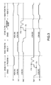
- FIG. 3 is a timing diagram of the store and read operations for each of the two, series-connected, non-volatile memory cells in the stack of the NAND stack EEPROM shown in FIG. 2 .
- FIG. 1 illustrates a NAND stack EEPROM with random programming capability 10 , hereinafter EEPROM 10 .
- the EEPROM 10 includes a memory array 12 for storing bits of data received from the exterior environment, a controller 14 for processing commands from a microprocessor or similar device relating to data to be transferred between the memory array 12 and the exterior environment, and input/output circuitry 16 for receiving bits of data from that exterior environment that are to be stored in the memory array 12 and providing bits of data that have been stored in the memory array 12 to the exterior environment. While the memory array 12 , controller 14 , and input/output circuitry 16 are shown as being integrated onto a single semiconductor chip it should be appreciated that all or part of each of these elements could be located on a separate chip or chips.
- the memory array 12 is comprised of a plurality of memory stacks 18 A- 18 N.
- Each of the memory stacks 18 A- 18 N includes a first end 20 A- 20 N that is connected to a bit line 22 A- 22 N and a second end 24 A- 24 N that is connected to a reference line or ground 26 .
- Located between the first and second ends of each the memory stacks are eight, series-connected, non-volatile memory devices 28 A 1 - 28 A 8 , 28 B 1 - 28 B 8 and 28 N 1 - 28 N 8 . While each stack includes eight non-volatile memory devices, it should be appreciated that a stack includes at least two, non-volatile memory devices and may have eight or more, non-volatile memory devices.
- the non-volatile memory devices are silicon nitride oxide semiconductor, n-channel, field-effect transistors, i.e., SNOS FETs. It should be appreciated that while n-channel FETs are utilized in the illustrated embodiment, with appropriate modifications, p-channel devices can also be utilized. Further, several other types of non-volatile memory devices that have adjustable thresholds are also feasible, including silicon oxide nitride oxide semiconductor transistors (SONOS), floating gate transistors and ferroelectric transistors.
- SONOS silicon oxide nitride oxide semiconductor transistors
- the gates of the first non-volatile memory device 28 A 1 - 28 N 1 in each of the stacks 18 A- 18 N is connected to the controller 14 by a V SE1 line. Likewise, the gates of the second through eighth corresponding non-volatile memory devices in each of the stacks are respectively connected to the controller via V SE2 -V SE8 lines.
- Each of the memory stacks includes a first switching device 30 A- 30 N located between the bit lines 22 A- 22 N and the first non-volatile memory devices 28 A 1 - 28 N 1 for operatively connecting and disconnecting a stack from its associated bit line.
- each of the first switching devices is an n-channel, field-effect transistor. It should be appreciated that with appropriate modifications, p-channel FETS, bipolar transistors and combinations of different types of transistors can be utilized.
- the gate of each of the first switching devices 30 A- 30 N is connected to the controller via a V STR line.
- Each of the memory stacks further includes a second switching device 32 A- 32 N located between the second ends 24 A- 24 N and the eighth non-volatile memory devices 28 A 8 - 28 N 8 for operatively connecting and disconnecting a stack from ground 26 .
- a second switching device 32 A- 32 N located between the second ends 24 A- 24 N and the eighth non-volatile memory devices 28 A 8 - 28 N 8 for operatively connecting and disconnecting a stack from ground 26 .
- n-channel FETs are utilized but other types of transistors and combinations can also be used, as noted with respect to the first switching devices.
- the gate of each of the second switching devices 32 A- 32 N is connected to the controller via V RCL line.
- the controller 14 manages the V STR , V RCL and V SE1 -V SE8 lines so that non-volatile memory devices in each of the stacks 18 A- 18 N can be programmed in any order, i.e., in random order.
- the second non-volatile memory devices 28 A 2 - 28 N 2 can be programmed before the seventh non-volatile memory devices 28 A 7 - 28 N 7 .
- the random programming capability is described with respect to a NAND stack EEPROM 50 (FIG. 2) that includes a controller 52 and single stack 54 with a first end 56 and a second end 58 .
- a bit line (bl) is operatively connected to the to the first end 56 of the stack 54 .
- the second end 58 of the stack is connected to a ground 60 .
- the two, non-volatile memory devices 62 A and 62 B are respectively connected to the controller 52 by V SE1 and V SE2 lines.
- the first switching device 64 and second switching device 66 are respectively connected to the controller 52 via V STR and V RCL lines.
- the sense amplifier and other I/O circuitry are not shown.
- FIG. 3 illustrates each of the following operations associated with the EEPROM 50 : (1) a store operation to the first non-volatile memory cell 62 A (tn 1 ); a store operation to the second non-volatile memory cell 62 B (tn 2 ); (3) a read operation from the first non-volatile memory cell 62 A; and (4) a read operation from the second non-volatile memory cell 62 B. While FIG. 3 shows the store and read operations occurring in a particular sequence, these operations could occur in any sequence, i.e., could occur in a random sequence. It should be particularly appreciated, however, that the store operations could occur in a random sequence.
- the store operation with respect to the first non-volatile memory cell 62 A is described.
- the store operation typically occurs in response to a command received by the controller 52 .
- the store operation with respect to the first non-volatile memory cell 62 A includes an erase phase and a program phase.
- the controller 52 places the first non-volatile memory cell 62 A in a known state so that it can be subsequently programmed to reflect the state of the bit of data on the bit line (bl).
- the controller 52 places: (1) V STR in a LOW condition to turn OFF the first switching device 64 and thereby disconnect the bit line (bl) from the stack 54 ; (2) V RCL in a LOW condition to turn OFF the second switching device 66 and thereby disconnect the stack 54 from ground 60 ; and (3) V SE2 at the ground voltage, i.e., 0 volts.
- V SE1 in a LOW condition to put the gate of the first non-volatile memory cell 62 A in a neutral position; and (2) the bit line in a HIGH condition.
- the controller 14 transitions the V SE2 signal from ground to a large negative voltage (referred to as an erase voltage) to place the first non-volatile memory cell 62 A in a known condition.
- an erase voltage a large negative voltage
- the first non-volatile memory cell 62 A has a known depletion threshold voltage, e.g., ⁇ 2 V.
- the depletion threshold voltage is representative of a logical 0.
- the controller 52 causes the V SE2 signal to transition from the large negative voltage to ground.
- the erase phase takes approximately 6-8 ms to complete.
- the program phase of the store operation causes the thresholds of the first non-volatile memory cell 62 A to be set in a manner that reflects the value of the bit or signal present on the bit line (bl).
- the program operation commences with the controller establishing: (1) V STR in a HIGH condition to connect the bit line (bl) to the stack 54 ; (2) V RCL in the LOW condition to disconnect the stack 54 from ground 60 ; and (3) V SE2 in the LOW condition to place the second non-volatile memory cell gate in a neutral position.
- the bit line (bl) is placed in a LOW condition, which reflects that the state of the bit that is to be programmed into the first non-volatile memory cell 62 A is a logical 1 (if the bit was a logical 0, the bit line would be in a HIGH condition).
- the controller 52 cycles the V SE2 between ground and a large positive voltage whose magnitude is greater than the power supply voltage (referred to as a program voltage) to establish a new threshold voltage, e.g., +2V.
- the threshold of the first non-volatile memory cell 62 A is changed or “programmed” and the threshold of the second non-volatile memory cell 62 B is left unchanged or “program inhibited.”
- the controller 52 causes: (1) V SE2 to transition from the program voltage to ground; and (2) V STR to transition from the HIGH state to the LOW state to disconnect the stack 54 from the bit line (bl).
- the program phase takes approximately 1.5-2 ms to complete.
- the bit line read and write voltages are complimentary, i.e., a logical 0 is high during a write and low during a read. They can be made the same polarity by connecting the second end 58 to the positive power supply.
- the programming phase implements a program with respect to the first non-volatile memory cell 62 A and a dynamic program inhibit on the second non-volatile memory cell 62 B, which is not being programmed.
- the second non-volatile memory cell 626 is subjected to dynamic program inhibit. More specifically, because the second non-volatile memory cell 62 B and the second switching device 66 are each cut-off, no charge can be supplied to the second non-volatile memory cell 62 B.
- the surface potential directly beneath the grounded gate of the second non-volatile memory cell 62 B is close to the gate which is held at ground so that there is little or no voltage drop across the gate dielectric and, as a consequence, no tunneling of charge to change the threshold voltage.
- charge is available from the bit line.
- the surface potential of the first non-volatile memory cell 62 A is at ground, the programming voltage on V SE1 drops across the gate of the cell, and tunneling occurs across the ultra-thin oxide of the SNOS FET which leaves the nitride with a negative charge and the SNOS with a new threshold, e.g., +2V.
- the store operation with respect to the second non-volatile memory cell 62 B has both an erase phase and program phase, just as with the store operation for the first non-volatile memory cell 62 A.
- the controller 52 manages V STR and V RCL during the erase and program phases in the same manner as noted with respect to store operation for the first non-volatile memory cell 62 A.
- the controller 52 manages the V SE2 and the V SE1 signals differently. More specifically, for the duration of the erase phase, the controller 14 places V SE1 in a LOW condition to place the gate of the first non-volatile memory cell 62 A in a neutral position.
- the controller 52 establishes V SE2 at ground. Subsequently, the controller 52 causes V SE2 to transition from ground to a large negative voltage to establish the depletion threshold for the second non-volatile memory cell 62 B. Finally, at the end of the erase phase, the controller causes V SE2 to return to ground.
- the controller 52 places V SE1 in a HIGH condition to establish a connection between the bit line (bl) and the second non-volatile memory cell 62 B.
- the bit line (bl) is placed in a HIGH condition, which reflects that the state of the bit that is to be programmed into the first non-volatile memory cell 62 A is a logical 0.
- the value of the bit could also be a logical 1. In which case, the bit line would be in a LOW condition.
- the threshold voltage of for the second non-volatile memory cell 62 B will not change from the erase phase (if the bit was a logical 1, the bit line would be in a HIGH condition).
- dynamic program inhibit is utilized.
- the drain of the first non-volatile memory cell 62 A will rise to about 2V and the first non-volatile memory cell 62 A will be cut-off by first switching device 64 whose gate and drain are both in the HIGH condition and therefore, unable to provide any charge.
- V SE2 With all source of charge cut-off, V SE2 will couple to the surface directly beneath it as it rises up to the program voltage. With essentially no voltage across the dielectric of the second non-volatile memory cell 62 B, tunneling of charge is inhibited and the threshold voltage remains unchanged.
- dynamic program inhibit also prevent the first non-volatile memory cell from being programmed.
- dynamic program inhibit reduces the number of nodes within an EEPROM to which a high voltage must be applied during store operation relative to, for example, a static program inhibit. This, in turn, allows the elements of an EEPROM to be positioned closer to one another, thereby increasing the number of EEPROM memory cells that can established in a given area of an integrated circuit.
- the use of dynamic program inhibit in the store operations associated with both the first non-volatile memory cell 62 A and the second non-volatile memory cell 62 B permits the non-volatile memory cells to be randomly programmed, i.e., programmed in any order, because the high voltages are confined to the gates of the SNOS FETs and the underlying surfaces.
- the read operation with respect to the first non-volatile memory cell 62 A is described.
- the read operation typically occurs in response to a command received by the controller 52 .
- the controller 52 establishes each of V STR , V RCL , V SE1 and V SE2 in a LOW condition.
- the bit line is in a HIGH condition.
- the controller 52 places V STR , V RCL and V SE2 is a HIGH condition.
- the bit line (bl) does not discharge through the stack 54 because the first non-volatile memory cell 62 A gated by 0 V sinks essentially no current because it was last programmed into enhancement mode. Since the sense amplifier at the end of the bit line (bl) does not perceive any change in the state of the signal on the bit line, it interprets the signal on the bit line as a logical “1”.
- the controller 52 manages the state V STR and V RCL in the same manner as noted with respect to the first non-volatile memory cell 62 A. However, the controller 52 manages the V SE1 and V SE2 signals differently. Specifically, the controller 52 places V SE1 in a LOW condition at the beginning of the read operation and then causes V SE1 to transition to a HIGH condition. The controller 52 places V SE2 in a LOW condition for the duration of the read operation. The bit line (bl) is initially in a HIGH condition. However, since the second non-volatile memory cell 62 B is a depletion type transistor gated by 0V, the stack 54 sinks current. As a consequence, the signal on the bit line dips, which is interpreted by sense amplifier as a logical “0.”
- the read operations with respect to the first non-volatile memory cell 62 A and second non-volatile memory cell 62 B can occur in any order, i.e., in a random order.
- controller is depicted as being integrated onto the same chip as the nvSRAM cell or cells, the controller can also be implemented separately from the nvSRAM cells. Further, the controller and/or the memory cell can be integrated onto a chip that includes other componentry, such as logic circuits and microcontrollers.
Abstract
Description
Claims (5)
Priority Applications (1)
| Application Number | Priority Date | Filing Date | Title |
|---|---|---|---|
| US09/681,314 US6512694B2 (en) | 2001-03-16 | 2001-03-16 | NAND stack EEPROM with random programming capability |
Applications Claiming Priority (1)
| Application Number | Priority Date | Filing Date | Title |
|---|---|---|---|
| US09/681,314 US6512694B2 (en) | 2001-03-16 | 2001-03-16 | NAND stack EEPROM with random programming capability |
Publications (2)
| Publication Number | Publication Date |
|---|---|
| US20020131302A1 US20020131302A1 (en) | 2002-09-19 |
| US6512694B2 true US6512694B2 (en) | 2003-01-28 |
Family
ID=24734747
Family Applications (1)
| Application Number | Title | Priority Date | Filing Date |
|---|---|---|---|
| US09/681,314 Expired - Lifetime US6512694B2 (en) | 2001-03-16 | 2001-03-16 | NAND stack EEPROM with random programming capability |
Country Status (1)
| Country | Link |
|---|---|
| US (1) | US6512694B2 (en) |
Cited By (11)
| Publication number | Priority date | Publication date | Assignee | Title |
|---|---|---|---|---|
| US20030016562A1 (en) * | 2001-07-23 | 2003-01-23 | Samsung Electronics Co., Ltd. | Memory devices with page buffer having dual registers and methods of using the same |
| US20040100826A1 (en) * | 2002-11-26 | 2004-05-27 | Cho Myoung-Kwan | Method for operating nor type flash memory device including sonos cells |
| US20040125629A1 (en) * | 2002-12-31 | 2004-07-01 | Scheuerlein Roy E. | Programmable memory array structure incorporating series-connected transistor strings and methods for fabrication and operation of same |
| US20040145024A1 (en) * | 2002-12-31 | 2004-07-29 | En-Hsing Chen | NAND memory array incorporating capacitance boosting of channel regions in unselected memory cells and method for operation of same |
| US20050122780A1 (en) * | 2003-12-05 | 2005-06-09 | En-Hsing Chen | NAND memory array incorporating multiple write pulse programming of individual memory cells and method for operation of same |
| US20050128807A1 (en) * | 2003-12-05 | 2005-06-16 | En-Hsing Chen | Nand memory array incorporating multiple series selection devices and method for operation of same |
| US20070133304A1 (en) * | 2005-12-08 | 2007-06-14 | Elite Semiconductor Memory Technology Inc. | Method and apparatus for determining sensing timing of flash memory |
| US20070217263A1 (en) * | 2003-12-05 | 2007-09-20 | Fasoli Luca G | Memory array incorporating memory cells arranged in nand strings |
| DE102009053977B3 (en) * | 2009-11-23 | 2011-01-20 | Anvo-Systems Dresden Gmbh | Memory cell for use in non-volatile static random access memory circuit, comprises static random access memory storage cell for storage of information bits and non-volatile storage area |
| US8923049B2 (en) | 2011-09-09 | 2014-12-30 | Aplus Flash Technology, Inc | 1T1b and 2T2b flash-based, data-oriented EEPROM design |
| US10510417B2 (en) * | 2018-03-16 | 2019-12-17 | Toshiba Memory Corporation | Semiconductor memory device and memory system |
Families Citing this family (1)
| Publication number | Priority date | Publication date | Assignee | Title |
|---|---|---|---|---|
| US7295478B2 (en) * | 2005-05-12 | 2007-11-13 | Sandisk Corporation | Selective application of program inhibit schemes in non-volatile memory |
Citations (11)
| Publication number | Priority date | Publication date | Assignee | Title |
|---|---|---|---|---|
| US4142176A (en) | 1976-09-27 | 1979-02-27 | Mostek Corporation | Series read only memory structure |
| US4959812A (en) | 1987-12-28 | 1990-09-25 | Kabushiki Kaisha Toshiba | Electrically erasable programmable read-only memory with NAND cell structure |
| US5008856A (en) | 1987-06-29 | 1991-04-16 | Kabushiki Kaisha Toshiba | Electrically programmable nonvolatile semiconductor memory device with NAND cell structure |
| US5440509A (en) * | 1987-11-18 | 1995-08-08 | Kabushiki Kaisha Toshiba | Electrically erasable programmable read-only memory with NAND cell structure and intermediate level voltages initially applied to bit lines |
| US5546341A (en) | 1993-01-13 | 1996-08-13 | Samsung Electronics Co., Ltd. | Nonvolatile semiconductor memory |
| US5723888A (en) | 1993-05-17 | 1998-03-03 | Yu; Shih-Chiang | Non-volatile semiconductor memory device |
| US5798547A (en) | 1995-11-29 | 1998-08-25 | Nec Corporation | Non-volatile semiconductor memory device having NAND structure cells |
| US5892712A (en) | 1996-05-01 | 1999-04-06 | Nvx Corporation | Semiconductor non-volatile latch device including embedded non-volatile elements |
| US6009014A (en) * | 1998-06-03 | 1999-12-28 | Advanced Micro Devices, Inc. | Erase verify scheme for NAND flash |
| US6058046A (en) * | 1994-09-30 | 2000-05-02 | Kabushiki Kaisha Toshiba | Nonvolatile semiconductor memory cell capable of saving overwritten cell and its saving method |
| US6163048A (en) | 1995-10-25 | 2000-12-19 | Cypress Semiconductor Corporation | Semiconductor non-volatile memory device having a NAND cell structure |
-
2001
- 2001-03-16 US US09/681,314 patent/US6512694B2/en not_active Expired - Lifetime
Patent Citations (11)
| Publication number | Priority date | Publication date | Assignee | Title |
|---|---|---|---|---|
| US4142176A (en) | 1976-09-27 | 1979-02-27 | Mostek Corporation | Series read only memory structure |
| US5008856A (en) | 1987-06-29 | 1991-04-16 | Kabushiki Kaisha Toshiba | Electrically programmable nonvolatile semiconductor memory device with NAND cell structure |
| US5440509A (en) * | 1987-11-18 | 1995-08-08 | Kabushiki Kaisha Toshiba | Electrically erasable programmable read-only memory with NAND cell structure and intermediate level voltages initially applied to bit lines |
| US4959812A (en) | 1987-12-28 | 1990-09-25 | Kabushiki Kaisha Toshiba | Electrically erasable programmable read-only memory with NAND cell structure |
| US5546341A (en) | 1993-01-13 | 1996-08-13 | Samsung Electronics Co., Ltd. | Nonvolatile semiconductor memory |
| US5723888A (en) | 1993-05-17 | 1998-03-03 | Yu; Shih-Chiang | Non-volatile semiconductor memory device |
| US6058046A (en) * | 1994-09-30 | 2000-05-02 | Kabushiki Kaisha Toshiba | Nonvolatile semiconductor memory cell capable of saving overwritten cell and its saving method |
| US6163048A (en) | 1995-10-25 | 2000-12-19 | Cypress Semiconductor Corporation | Semiconductor non-volatile memory device having a NAND cell structure |
| US5798547A (en) | 1995-11-29 | 1998-08-25 | Nec Corporation | Non-volatile semiconductor memory device having NAND structure cells |
| US5892712A (en) | 1996-05-01 | 1999-04-06 | Nvx Corporation | Semiconductor non-volatile latch device including embedded non-volatile elements |
| US6009014A (en) * | 1998-06-03 | 1999-12-28 | Advanced Micro Devices, Inc. | Erase verify scheme for NAND flash |
Non-Patent Citations (1)
| Title |
|---|
| Herdt, Christian E. and Paz de Araujo, Carlos A., "Analysis, Measurement, and Simulation of Dynamic Write Inhibit in an nySRAM Cell", 1992, IEEE. |
Cited By (18)
| Publication number | Priority date | Publication date | Assignee | Title |
|---|---|---|---|---|
| US20030016562A1 (en) * | 2001-07-23 | 2003-01-23 | Samsung Electronics Co., Ltd. | Memory devices with page buffer having dual registers and methods of using the same |
| US6671204B2 (en) * | 2001-07-23 | 2003-12-30 | Samsung Electronics Co., Ltd. | Nonvolatile memory device with page buffer having dual registers and methods of using the same |
| US20040100826A1 (en) * | 2002-11-26 | 2004-05-27 | Cho Myoung-Kwan | Method for operating nor type flash memory device including sonos cells |
| US6847556B2 (en) * | 2002-11-26 | 2005-01-25 | Samsung Electronics Co., Ltd. | Method for operating NOR type flash memory device including SONOS cells |
| US20040125629A1 (en) * | 2002-12-31 | 2004-07-01 | Scheuerlein Roy E. | Programmable memory array structure incorporating series-connected transistor strings and methods for fabrication and operation of same |
| US20040145024A1 (en) * | 2002-12-31 | 2004-07-29 | En-Hsing Chen | NAND memory array incorporating capacitance boosting of channel regions in unselected memory cells and method for operation of same |
| US7433233B2 (en) | 2002-12-31 | 2008-10-07 | Sandisk 3D Llc | NAND memory array incorporating capacitance boosting of channel regions in unselected memory cells and method for operation of same |
| US7233522B2 (en) * | 2002-12-31 | 2007-06-19 | Sandisk 3D Llc | NAND memory array incorporating capacitance boosting of channel regions in unselected memory cells and method for operation of same |
| US7023739B2 (en) | 2003-12-05 | 2006-04-04 | Matrix Semiconductor, Inc. | NAND memory array incorporating multiple write pulse programming of individual memory cells and method for operation of same |
| US20050128807A1 (en) * | 2003-12-05 | 2005-06-16 | En-Hsing Chen | Nand memory array incorporating multiple series selection devices and method for operation of same |
| US20070217263A1 (en) * | 2003-12-05 | 2007-09-20 | Fasoli Luca G | Memory array incorporating memory cells arranged in nand strings |
| US20050122780A1 (en) * | 2003-12-05 | 2005-06-09 | En-Hsing Chen | NAND memory array incorporating multiple write pulse programming of individual memory cells and method for operation of same |
| US7508714B2 (en) | 2003-12-05 | 2009-03-24 | Sandisk 3D Llc | Memory array incorporating mirrored NAND strings and non-shared global bit lines within a block |
| US20070133304A1 (en) * | 2005-12-08 | 2007-06-14 | Elite Semiconductor Memory Technology Inc. | Method and apparatus for determining sensing timing of flash memory |
| US7263004B2 (en) * | 2005-12-08 | 2007-08-28 | Elite Semiconductor Memory Technology Inc. | Method and apparatus for determining sensing timing of flash memory |
| DE102009053977B3 (en) * | 2009-11-23 | 2011-01-20 | Anvo-Systems Dresden Gmbh | Memory cell for use in non-volatile static random access memory circuit, comprises static random access memory storage cell for storage of information bits and non-volatile storage area |
| US8923049B2 (en) | 2011-09-09 | 2014-12-30 | Aplus Flash Technology, Inc | 1T1b and 2T2b flash-based, data-oriented EEPROM design |
| US10510417B2 (en) * | 2018-03-16 | 2019-12-17 | Toshiba Memory Corporation | Semiconductor memory device and memory system |
Also Published As
| Publication number | Publication date |
|---|---|
| US20020131302A1 (en) | 2002-09-19 |
Similar Documents
| Publication | Publication Date | Title |
|---|---|---|
| US6414873B1 (en) | nvSRAM with multiple non-volatile memory cells for each SRAM memory cell | |
| US7539054B2 (en) | Method and apparatus to program and erase a non-volatile static random access memory from the bit lines | |
| US4435786A (en) | Self-refreshing memory cell | |
| US5517449A (en) | Memory cell of nonvolatile semiconductor memory device | |
| EP0880143B1 (en) | A non-volatile memory device and method for programming | |
| US6097629A (en) | Non-volatile, static random access memory with high speed store capability | |
| US7518916B2 (en) | Method and apparatus to program both sides of a non-volatile static random access memory | |
| EP0028935B1 (en) | Nonvolatile semiconductor memory circuits | |
| US5914895A (en) | Non-volatile random access memory and methods for making and configuring same | |
| US7339829B2 (en) | Ultra low power non-volatile memory module | |
| EP0551926A1 (en) | Nonvolatile semiconductor memory device | |
| US4733371A (en) | Semiconductor memory device with high voltage switch | |
| JPH0715797B2 (en) | Microcomputer equipped with non-volatile RAM memory | |
| EP0426282B1 (en) | Programmable logic device | |
| US6512694B2 (en) | NAND stack EEPROM with random programming capability | |
| US20060291319A1 (en) | Reduced area high voltage switch for NVM | |
| US20080151654A1 (en) | Method and apparatus to implement a reset function in a non-volatile static random access memory | |
| EP0334550B1 (en) | Nonvolatile RAM cell | |
| US20060023514A1 (en) | Semiconductor nonvolatile storage device | |
| KR900001774B1 (en) | The semiconductor memory device involving a bias voltage generator | |
| US5930175A (en) | Voltage pump switch | |
| US5287307A (en) | Semiconductor memory device | |
| JP3998908B2 (en) | Nonvolatile memory device | |
| US5978263A (en) | Negative voltage switch architecture for a nonvolatile memory | |
| EP0830686A1 (en) | Negative voltage switching circuit |
Legal Events
| Date | Code | Title | Description |
|---|---|---|---|
| AS | Assignment |
Owner name: SIMTEK CORPORATION, COLORADO Free format text: ASSIGNMENT OF ASSIGNORS INTEREST;ASSIGNOR:HERDT, CHRISTIAN E.;REEL/FRAME:011630/0598 Effective date: 20010330 |
|
| STCF | Information on status: patent grant |
Free format text: PATENTED CASE |
|
| CC | Certificate of correction | ||
| FPAY | Fee payment |
Year of fee payment: 4 |
|
| AS | Assignment |
Owner name: SIMTEK CORPORATION, COLORADO Free format text: STATUTORY CONVERSION;ASSIGNOR:SIMTEK CORPORATION;REEL/FRAME:018552/0829 Effective date: 20061005 |
|
| FEPP | Fee payment procedure |
Free format text: PAYOR NUMBER ASSIGNED (ORIGINAL EVENT CODE: ASPN); ENTITY STATUS OF PATENT OWNER: LARGE ENTITY |
|
| AS | Assignment |
Owner name: CYPRESS SEMICONDUCTOR CORPORATION, CALIFORNIA Free format text: ASSIGNMENT OF ASSIGNORS INTEREST;ASSIGNOR:SIMTEK CORPORATION;REEL/FRAME:022878/0228 Effective date: 20081030 |
|
| REMI | Maintenance fee reminder mailed | ||
| FEPP | Fee payment procedure |
Free format text: PAT HOLDER NO LONGER CLAIMS SMALL ENTITY STATUS, ENTITY STATUS SET TO UNDISCOUNTED (ORIGINAL EVENT CODE: STOL); ENTITY STATUS OF PATENT OWNER: LARGE ENTITY |
|
| FPAY | Fee payment |
Year of fee payment: 8 |
|
| SULP | Surcharge for late payment |
Year of fee payment: 7 |
|
| FPAY | Fee payment |
Year of fee payment: 12 |
|
| AS | Assignment |
Owner name: MORGAN STANLEY SENIOR FUNDING, INC., NEW YORK Free format text: SECURITY INTEREST;ASSIGNORS:CYPRESS SEMICONDUCTOR CORPORATION;SPANSION LLC;REEL/FRAME:035240/0429 Effective date: 20150312 |
|
| AS | Assignment |
Owner name: MONTEREY RESEARCH, LLC, CALIFORNIA Free format text: ASSIGNMENT OF ASSIGNORS INTEREST;ASSIGNOR:CYPRESS SEMICONDUCTOR CORPORATION;REEL/FRAME:040908/0979 Effective date: 20161209 |
|
| AS | Assignment |
Owner name: CYPRESS SEMICONDUCTOR CORPORATION, CALIFORNIA Free format text: RELEASE BY SECURED PARTY;ASSIGNOR:MORGAN STANLEY SENIOR FUNDING, INC.;REEL/FRAME:041178/0061 Effective date: 20161209 Owner name: SPANSION LLC, CALIFORNIA Free format text: RELEASE BY SECURED PARTY;ASSIGNOR:MORGAN STANLEY SENIOR FUNDING, INC.;REEL/FRAME:041178/0061 Effective date: 20161209 |
|
| AS | Assignment |
Owner name: MORGAN STANLEY SENIOR FUNDING, INC., NEW YORK Free format text: CORRECTIVE ASSIGNMENT TO CORRECT THE 8647899 PREVIOUSLY RECORDED ON REEL 035240 FRAME 0429. ASSIGNOR(S) HEREBY CONFIRMS THE SECURITY INTERST;ASSIGNORS:CYPRESS SEMICONDUCTOR CORPORATION;SPANSION LLC;REEL/FRAME:058002/0470 Effective date: 20150312 |