US6518666B1 - Circuit board reducing a warp and a method of mounting an integrated circuit chip - Google Patents
Circuit board reducing a warp and a method of mounting an integrated circuit chip Download PDFInfo
- Publication number
- US6518666B1 US6518666B1 US09/667,522 US66752200A US6518666B1 US 6518666 B1 US6518666 B1 US 6518666B1 US 66752200 A US66752200 A US 66752200A US 6518666 B1 US6518666 B1 US 6518666B1
- Authority
- US
- United States
- Prior art keywords
- wiring board
- lsi
- chip
- integrated circuit
- plural
- Prior art date
- Legal status (The legal status is an assumption and is not a legal conclusion. Google has not performed a legal analysis and makes no representation as to the accuracy of the status listed.)
- Expired - Fee Related
Links
Images


Classifications
-
- H—ELECTRICITY
- H05—ELECTRIC TECHNIQUES NOT OTHERWISE PROVIDED FOR
- H05K—PRINTED CIRCUITS; CASINGS OR CONSTRUCTIONAL DETAILS OF ELECTRIC APPARATUS; MANUFACTURE OF ASSEMBLAGES OF ELECTRICAL COMPONENTS
- H05K1/00—Printed circuits
- H05K1/02—Details
- H05K1/0271—Arrangements for reducing stress or warp in rigid printed circuit boards, e.g. caused by loads, vibrations or differences in thermal expansion
-
- H—ELECTRICITY
- H01—ELECTRIC ELEMENTS
- H01L—SEMICONDUCTOR DEVICES NOT COVERED BY CLASS H10
- H01L23/00—Details of semiconductor or other solid state devices
- H01L23/34—Arrangements for cooling, heating, ventilating or temperature compensation ; Temperature sensing arrangements
- H01L23/36—Selection of materials, or shaping, to facilitate cooling or heating, e.g. heatsinks
- H01L23/373—Cooling facilitated by selection of materials for the device or materials for thermal expansion adaptation, e.g. carbon
- H01L23/3735—Laminates or multilayers, e.g. direct bond copper ceramic substrates
-
- H—ELECTRICITY
- H05—ELECTRIC TECHNIQUES NOT OTHERWISE PROVIDED FOR
- H05K—PRINTED CIRCUITS; CASINGS OR CONSTRUCTIONAL DETAILS OF ELECTRIC APPARATUS; MANUFACTURE OF ASSEMBLAGES OF ELECTRICAL COMPONENTS
- H05K1/00—Printed circuits
- H05K1/02—Details
- H05K1/0213—Electrical arrangements not otherwise provided for
- H05K1/0216—Reduction of cross-talk, noise or electromagnetic interference
- H05K1/023—Reduction of cross-talk, noise or electromagnetic interference using auxiliary mounted passive components or auxiliary substances
- H05K1/0231—Capacitors or dielectric substances
-
- H—ELECTRICITY
- H01—ELECTRIC ELEMENTS
- H01L—SEMICONDUCTOR DEVICES NOT COVERED BY CLASS H10
- H01L2224/00—Indexing scheme for arrangements for connecting or disconnecting semiconductor or solid-state bodies and methods related thereto as covered by H01L24/00
- H01L2224/01—Means for bonding being attached to, or being formed on, the surface to be connected, e.g. chip-to-package, die-attach, "first-level" interconnects; Manufacturing methods related thereto
- H01L2224/10—Bump connectors; Manufacturing methods related thereto
- H01L2224/15—Structure, shape, material or disposition of the bump connectors after the connecting process
- H01L2224/16—Structure, shape, material or disposition of the bump connectors after the connecting process of an individual bump connector
- H01L2224/161—Disposition
- H01L2224/16151—Disposition the bump connector connecting between a semiconductor or solid-state body and an item not being a semiconductor or solid-state body, e.g. chip-to-substrate, chip-to-passive
- H01L2224/16221—Disposition the bump connector connecting between a semiconductor or solid-state body and an item not being a semiconductor or solid-state body, e.g. chip-to-substrate, chip-to-passive the body and the item being stacked
- H01L2224/16225—Disposition the bump connector connecting between a semiconductor or solid-state body and an item not being a semiconductor or solid-state body, e.g. chip-to-substrate, chip-to-passive the body and the item being stacked the item being non-metallic, e.g. insulating substrate with or without metallisation
-
- H—ELECTRICITY
- H01—ELECTRIC ELEMENTS
- H01L—SEMICONDUCTOR DEVICES NOT COVERED BY CLASS H10
- H01L2224/00—Indexing scheme for arrangements for connecting or disconnecting semiconductor or solid-state bodies and methods related thereto as covered by H01L24/00
- H01L2224/01—Means for bonding being attached to, or being formed on, the surface to be connected, e.g. chip-to-package, die-attach, "first-level" interconnects; Manufacturing methods related thereto
- H01L2224/26—Layer connectors, e.g. plate connectors, solder or adhesive layers; Manufacturing methods related thereto
- H01L2224/31—Structure, shape, material or disposition of the layer connectors after the connecting process
- H01L2224/32—Structure, shape, material or disposition of the layer connectors after the connecting process of an individual layer connector
- H01L2224/321—Disposition
- H01L2224/32151—Disposition the layer connector connecting between a semiconductor or solid-state body and an item not being a semiconductor or solid-state body, e.g. chip-to-substrate, chip-to-passive
- H01L2224/32221—Disposition the layer connector connecting between a semiconductor or solid-state body and an item not being a semiconductor or solid-state body, e.g. chip-to-substrate, chip-to-passive the body and the item being stacked
- H01L2224/32225—Disposition the layer connector connecting between a semiconductor or solid-state body and an item not being a semiconductor or solid-state body, e.g. chip-to-substrate, chip-to-passive the body and the item being stacked the item being non-metallic, e.g. insulating substrate with or without metallisation
-
- H—ELECTRICITY
- H01—ELECTRIC ELEMENTS
- H01L—SEMICONDUCTOR DEVICES NOT COVERED BY CLASS H10
- H01L2224/00—Indexing scheme for arrangements for connecting or disconnecting semiconductor or solid-state bodies and methods related thereto as covered by H01L24/00
- H01L2224/73—Means for bonding being of different types provided for in two or more of groups H01L2224/10, H01L2224/18, H01L2224/26, H01L2224/34, H01L2224/42, H01L2224/50, H01L2224/63, H01L2224/71
- H01L2224/732—Location after the connecting process
- H01L2224/73201—Location after the connecting process on the same surface
- H01L2224/73203—Bump and layer connectors
- H01L2224/73204—Bump and layer connectors the bump connector being embedded into the layer connector
-
- H—ELECTRICITY
- H01—ELECTRIC ELEMENTS
- H01L—SEMICONDUCTOR DEVICES NOT COVERED BY CLASS H10
- H01L2224/00—Indexing scheme for arrangements for connecting or disconnecting semiconductor or solid-state bodies and methods related thereto as covered by H01L24/00
- H01L2224/73—Means for bonding being of different types provided for in two or more of groups H01L2224/10, H01L2224/18, H01L2224/26, H01L2224/34, H01L2224/42, H01L2224/50, H01L2224/63, H01L2224/71
- H01L2224/732—Location after the connecting process
- H01L2224/73251—Location after the connecting process on different surfaces
- H01L2224/73253—Bump and layer connectors
-
- H—ELECTRICITY
- H01—ELECTRIC ELEMENTS
- H01L—SEMICONDUCTOR DEVICES NOT COVERED BY CLASS H10
- H01L2924/00—Indexing scheme for arrangements or methods for connecting or disconnecting semiconductor or solid-state bodies as covered by H01L24/00
- H01L2924/01—Chemical elements
- H01L2924/01019—Potassium [K]
-
- H—ELECTRICITY
- H01—ELECTRIC ELEMENTS
- H01L—SEMICONDUCTOR DEVICES NOT COVERED BY CLASS H10
- H01L2924/00—Indexing scheme for arrangements or methods for connecting or disconnecting semiconductor or solid-state bodies as covered by H01L24/00
- H01L2924/01—Chemical elements
- H01L2924/01079—Gold [Au]
-
- H—ELECTRICITY
- H01—ELECTRIC ELEMENTS
- H01L—SEMICONDUCTOR DEVICES NOT COVERED BY CLASS H10
- H01L2924/00—Indexing scheme for arrangements or methods for connecting or disconnecting semiconductor or solid-state bodies as covered by H01L24/00
- H01L2924/19—Details of hybrid assemblies other than the semiconductor or other solid state devices to be connected
- H01L2924/191—Disposition
- H01L2924/19101—Disposition of discrete passive components
- H01L2924/19106—Disposition of discrete passive components in a mirrored arrangement on two different side of a common die mounting substrate
-
- H—ELECTRICITY
- H01—ELECTRIC ELEMENTS
- H01L—SEMICONDUCTOR DEVICES NOT COVERED BY CLASS H10
- H01L2924/00—Indexing scheme for arrangements or methods for connecting or disconnecting semiconductor or solid-state bodies as covered by H01L24/00
- H01L2924/30—Technical effects
- H01L2924/35—Mechanical effects
- H01L2924/351—Thermal stress
- H01L2924/3511—Warping
-
- H—ELECTRICITY
- H05—ELECTRIC TECHNIQUES NOT OTHERWISE PROVIDED FOR
- H05K—PRINTED CIRCUITS; CASINGS OR CONSTRUCTIONAL DETAILS OF ELECTRIC APPARATUS; MANUFACTURE OF ASSEMBLAGES OF ELECTRICAL COMPONENTS
- H05K2201/00—Indexing scheme relating to printed circuits covered by H05K1/00
- H05K2201/06—Thermal details
- H05K2201/068—Thermal details wherein the coefficient of thermal expansion is important
-
- H—ELECTRICITY
- H05—ELECTRIC TECHNIQUES NOT OTHERWISE PROVIDED FOR
- H05K—PRINTED CIRCUITS; CASINGS OR CONSTRUCTIONAL DETAILS OF ELECTRIC APPARATUS; MANUFACTURE OF ASSEMBLAGES OF ELECTRICAL COMPONENTS
- H05K2201/00—Indexing scheme relating to printed circuits covered by H05K1/00
- H05K2201/10—Details of components or other objects attached to or integrated in a printed circuit board
- H05K2201/10431—Details of mounted components
- H05K2201/10507—Involving several components
- H05K2201/10545—Related components mounted on both sides of the PCB
-
- H—ELECTRICITY
- H05—ELECTRIC TECHNIQUES NOT OTHERWISE PROVIDED FOR
- H05K—PRINTED CIRCUITS; CASINGS OR CONSTRUCTIONAL DETAILS OF ELECTRIC APPARATUS; MANUFACTURE OF ASSEMBLAGES OF ELECTRICAL COMPONENTS
- H05K2201/00—Indexing scheme relating to printed circuits covered by H05K1/00
- H05K2201/10—Details of components or other objects attached to or integrated in a printed circuit board
- H05K2201/10613—Details of electrical connections of non-printed components, e.g. special leads
- H05K2201/10621—Components characterised by their electrical contacts
- H05K2201/10674—Flip chip
-
- H—ELECTRICITY
- H05—ELECTRIC TECHNIQUES NOT OTHERWISE PROVIDED FOR
- H05K—PRINTED CIRCUITS; CASINGS OR CONSTRUCTIONAL DETAILS OF ELECTRIC APPARATUS; MANUFACTURE OF ASSEMBLAGES OF ELECTRICAL COMPONENTS
- H05K2201/00—Indexing scheme relating to printed circuits covered by H05K1/00
- H05K2201/20—Details of printed circuits not provided for in H05K2201/01 - H05K2201/10
- H05K2201/2009—Reinforced areas, e.g. for a specific part of a flexible printed circuit
-
- H—ELECTRICITY
- H05—ELECTRIC TECHNIQUES NOT OTHERWISE PROVIDED FOR
- H05K—PRINTED CIRCUITS; CASINGS OR CONSTRUCTIONAL DETAILS OF ELECTRIC APPARATUS; MANUFACTURE OF ASSEMBLAGES OF ELECTRICAL COMPONENTS
- H05K3/00—Apparatus or processes for manufacturing printed circuits
- H05K3/0058—Laminating printed circuit boards onto other substrates, e.g. metallic substrates
-
- H—ELECTRICITY
- H05—ELECTRIC TECHNIQUES NOT OTHERWISE PROVIDED FOR
- H05K—PRINTED CIRCUITS; CASINGS OR CONSTRUCTIONAL DETAILS OF ELECTRIC APPARATUS; MANUFACTURE OF ASSEMBLAGES OF ELECTRICAL COMPONENTS
- H05K3/00—Apparatus or processes for manufacturing printed circuits
- H05K3/22—Secondary treatment of printed circuits
- H05K3/28—Applying non-metallic protective coatings
- H05K3/284—Applying non-metallic protective coatings for encapsulating mounted components
Definitions
- the present invention relates to a circuit board and a method of mounting an integrated circuit chip, as a chip-on-board (COB).
- COB chip-on-board
- LSI An integrated circuit chip
- LSI can be mounted on a wiring board as a flip chip and a connection thereto sealed with resin.
- the coefficient of thermal expansion of the wiring board is large, compared with that of the LSI.
- the portion where the LSI is mounted is easily deformed on the side where LSI is mounted, because a difference in coefficients of thermal expansion between the wiring board and LSI causes a convex warp.
- a COB 100 may include active elements such as LSI 101 and a driver IC 112 , a passive element such as a tantalum capacitor 112 a , a chip capacitor 112 b and a connector 112 c mounted on wiring board 102 .
- Sealing resin 103 is injected between LSI 101 and the wiring board 102 , and a heat sink 110 for outgoing radiation is attached on LSI 101 via a thermal conduction member.
- the chip capacitor 112 b that functions as a bypass capacitor of each LSI 101 is also soldered on the wiring board 102 .
- Each terminal of the connector 112 c is connected to LSI 101 and others via wiring provided on the surface or inside the wiring board 102 . Therefore, COB 100 is electrically connected to an external device via the connector 112 c.
- the thickness of a thermal conduction member 109 is not uniform.
- the heat resistance increases, degrading the outgoing radiation.
- the warp of the LSI may change, causing peeling of the thermal conduction member 109 .
- the LSI may crack.
- Japanese published unexamined patent application No. Hei 10-229102 discloses a technique for preventing an LSI chip from being warped by mounting another LSI chip on the back of a wiring board opposite to the LSI chip mounted on the wiring board is.
- this technique can be applied only when two LSI chips having the same shape are packaged as one pair.
- solder bumps are generally provided on one side of an LSI chip. If an LSI chip is mounted on both sides of a wiring board, then an electrode pad is also required to be provided on both sides of the wiring board. Therefore, the structure of the wiring board becomes very complex and the manufacture is difficult. In the future, as large scale integrated circuits are enlarged, the number of the pins will increase. From the viewpoint of manufacturing a wiring board, it is not good policy to adopt the technique disclosed in the above-noted patent application to prevent the LSI from being warped.
- the invention is made to solve the above-described problems and the object is to provide the circuit board and the method of mounting an integrated circuit chip wherein the warp of the LSI can easily be reduced when plural LSIs are mounted on a wiring board.
- the circuit board according to the invention is based upon the structure of an integrated circuit chip provided with a wiring board and a plurality of integrated circuit chips mounted on the wiring board, at least one of the integrated circuit chips is mounted on a first surface of the wiring board as a flip chip with a sealing resin, and a bare plate is mounted with a resin directly opposite the integrated circuit chip on a second surface of the wiring board opposite the first surface.
- the invention inhibits the warp of the LSI as described above. Furthermore, the structure where the effect of outgoing radiation is high can be acquired by providing a uniformly thin thermal conduction member on a face where a heat sink and LSI are bonded. Also, in the structure, arranging the chip capacitor on the wiring board between the plate on the second surface and the wiring board can inhibit the rapid variation in voltage of the LSI, and high-speed operation can be realized.
- FIG. 1 is a sectional view showing a first embodiment according to the invention
- FIG. 2 is a first sectional view showing the manufacturing process of the circuit board shown in FIG. 1;
- FIG. 3 is a second sectional view showing the manufacturing process
- FIG. 4 is a third sectional view of manufacturing process
- FIG. 5 is a fourth sectional view of manufacturing process
- FIG. 6 is a sectional view showing a second embodiment according to the invention.
- FIG. 7 is a sectional view showing the second embodiment
- FIGS. 8 ( a ) to 8 ( c ) are plans showing layouts of chip capacitors
- FIG. 9 is a graph showing relationship between the coefficient of thermal expansion of a bare plate and a warp of LSI;
- FIG. 10 is a graph showing relationship between the thickness of the bare plate and a warp of LSI
- FIG. 11 is a graph showing relationship between the number of chip capacitors and a warp of LSI
- FIGS. 12 ( a ) to 12 ( c ) are plans showing layouts of chip capacitors
- FIG. 13 is a graph showing relationship between a layout of chip capacitors and a warp of LSI
- FIGS. 14 ( a ) to 14 ( l ) are sectional views showing the manufacturing process of the structure shown in FIG. 7;
- FIG. 15 is a perspective view showing general COB.
- FIG. 16 is a sectional view showing an example of prior art.
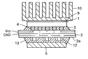
- pads corresponding to the arrangement of electrodes in LSI 1 are provided on a first surface of a wiring board 2 , and the electrodes in LSI 1 and pads on the wiring board 2 are connected in the form of a flip chip.
- the electrodes are arranged on the periphery of LSI 1 or in the form of a grid and are connected via conductive material such as solder.
- sealing resin 3 is filled in a connection with LSI 1 to mechanically reinforce the connection with LSI 1 and to prevent the infiltration of moisture from the outside and corrosion.
- a bare plate 5 is arranged opposite to LSI 1 on a second surface of the wiring board 2 opposite the first surface, and is fixed via sealing resin 13 .
- the coefficient of thermal expansion of the bare plate 5 arranged on the second surface of the wiring board 2 is equal to or less than that of the wiring board 2 and the lateral and longitudinal dimensions of the bare plate 5 are approximately equal to those of LSI 1 .
- the inventors have verified by experiments that the lateral and longitudinal dimensions of the bare plate 5 have only to be within 80 to 120% of the lateral and longitudinal dimensions of LSI 1 . If LSI 1 is a square one side of which is 20 mm 2 , the bare plate 5 has only to be a square one side of which is 16 to 24 mm 2 .
- the coefficient of thermal expansion of the wiring board 2 is large, compared with that of LSI 1 . Therefore, a convex warp is caused on the side where LSI 1 is mounted because of difference in a coefficients of thermal expansion between the wiring board 2 and LSI 1 in a state where no flat plate is arranged on the back of the wiring board 2 as in an example of the prior art.
- the apparent thickness of the wiring board is increased by fixing a bare plate 5 made of material having the same coefficient of thermal expansion as that of the wiring board 2 in this embodiment, the rigidity of the wiring board 2 is enhanced, the warp of LSI 1 can be reduced.
- pads corresponding to the arrangement of electrodes of LSI 1 are provided on the wiring board 2 and are electrically connected to the electrodes of LSI 1 by soldering and others.
- spherical solder bumps for example, Sn 63 /Pb 37 wt % or Sn 5 /Pb 95 wt % are provided beforehand to the electrodes of LSI 1
- cream solder for example, Sn 63 /Pb 37 wt %) is printed beforehand on each pad of the wiring board 2 .
- LSI 1 is mounted so that the pad of the wiring board 2 and the solder bumps of LSI 1 are opposite and the connection of the wiring board 2 and LSI 1 is completed by performing heating reflowing (for example at 210° C.) in a hot blast stove or similar technique and cooling.
- LSI 1 and the wiring board 2 are mechanically fixed when temperature is lower than the solidification line of solder (for example, in the case of solder made of Sn of 63 wt % and Pb of 37 wt %, 183° C.) While it is being restored from high temperature to room temperature (for example, 25° C.), LSI 1 and the wiring board 2 contract. Since the coefficient of thermal expansion of the wiring board 2 is larger than that of LSI 1 , the quantity of contraction is also large and as temperature lowers, a convex warp is caused on the side on which LSI 1 is mounted. Thermal stress caused by difference in a coefficient of thermal expansion between the wiring board 2 and LSI 1 concentrates at the connection 4 . In the case of soldering, as solder is relatively soft material, deformation is caused and as a result, a small warp 6 is caused.
- soldering as solder is relatively soft material, deformation is caused and as a result, a small warp 6 is caused.
- liquid sealing resin is filled from the periphery of LSI 1 .
- the sealing resin 3 is epoxy or thermoplastic insulating resin and is filled at temperature (for example, 60° C.) suitable for the fluidity of sealing resin to fill in small clearance between LSI 1 and the wiring board 2 .
- Sealing resin 3 is required to be filled to secure the reliability of connection in the connection 4 . Filling is normally started from one side or adjacent two sides of LSI 1 , taking care not to include bubbles in the connection 4 . After filling is completed, sealing resin 3 is heated to harden it (for example, at 150° C. for 30 minutes).
- LSI 1 and the wiring board 2 are thermally expanded again during heating, the existing convex warp on the side of LSI is reduced and becomes flatter.
- thermal contraction is caused again and as LSI 1 and the wiring board 2 are completely fixed via the sealing resin 3 , a convex large warp 8 is caused on the side where LSI 1 is mounted.
- a warp of approximately 50 to 100 ⁇ m may be caused.
- FIG. 4 is a sectional view showing structure in which LSI 1 is mounted on the wiring board 2 as a flip chip, sealing resin 3 is filled in the connection 4 and the bare plate 5 is arranged directly opposite the LSI 1 on the second surface of the wiring board 2 opposite the first surface.
- the wiring board 2 is turned upside down so that the back, that is second surface, is located on the upside, the sealing resin 13 is placed in the center portion opposite the LSI 1 , the bare plate 5 is pressed on the sealing resin 13 and heat hardening is performed in that state.
- the sealing resin 3 used for filling the connection 4 is used for the material of the sealing resin 13
- LSI 1 and the wiring board 2 are thermally expanded again because heat hardening temperature is 150° C. and when temperature reaches 150° C., a warp is reduced.
- the sealing resin 13 is hardened in this state, the quantity of a warp after cooling depends upon the material of the flat plate.
- a warp can be reduced by using material smaller in a coefficient of thermal expansion than that of the wiring board 2 such as alumina ceramics (approximately 7 ppm/° C., a 42 alloy (approximately 6 ppm/° C.), zirconia (approximately 11 ppm/° C.) and forsterite (approximately 10 ppm/° C.) for the bare plate 5 .
- alumina ceramics approximately 7 ppm/° C., a 42 alloy (approximately 6 ppm/° C.), zirconia (approximately 11 ppm/° C.) and forsterite (approximately 10 ppm/° C.) for the bare plate 5 .
- a heat sink is attached on the back of LSI 1 .
- the heat sink 10 aluminum which is excellent in a radiation characteristic and others are desirable and the heat sink is attached on a surface of LSI 1 opposite the wiring board 2 via a thermal conduction member 9 .
- the thermal conduction member 9 is made of material excellent in thermal conductivity and for example, epoxy resin including silver filler, a silicone compound including alumina ceramics filler and others are used. As a warp is reduced on the back of LSI 1 owing to effect produced by the bare plate 5 , the thermal conduction member for transmitting the heat of LSI 1 to the heat sink 10 can be uniformly thin and the effect of efficient radiation can be acquired.
- the warping of LSI 1 can be reduced by arranging the bare plate 5 on the second surface of the wiring board opposite the first surface where the LSI 1 is mounted as a flip chip. Furthermore, as the thermal conduction member provided on the surface on which the heat sink and LSI are bonded can be uniformly thinned, LSI package structure having enhanced effect of radiation can be acquired.
- Pads corresponding to the arrangement of electrodes of LSI 1 are provided on a first surface of a wiring board 2 , and the electrodes of LSI 1 and the pads of the wiring board 2 are electrically connected in the form of a flip chip.
- the electrodes are arranged in the periphery of LSI or in the form of a grid and are connected via conductive material such as solder.
- sealing resin 3 is filled in a connection with LSI 1 to mechanically reinforce the connection with LSI 1 and to prevent the infiltration of moisture from the outside and corrosion.
- Pads on which chip capacitors 12 are mounted are provided in an area having substantially the same outline as that of LSI 1 on a second surface of the wiring board 2 opposite a first surface where LSI 1 is mounted.
- the chip capacitor 12 is electrically connected to the pad, further a bare plate 5 is arranged on the chip capacitor 12 , and the wiring board 2 and the bare plate 5 are fixed via sealing resin 13 .
- the chip capacitor 12 functions as a bypass capacitor provided to reduce noise voltage generated on a power line and a ground line and is provided between a power source Vcc and a ground GND.
- the structure reduces the warping of LSI 1 to substantially zero as in the structure having no chip capacitor shown in FIG. 1 . Furthermore, as the chip capacitor is arranged just directly opposite the LSI 1 on the second surface of the wiring board 2 opposite the first surface, the structure has the effect of inhibiting the variation of the voltage of LSI 1 and is suitable for high-speed operation.
- cream solder for mounting the chip capacitor is printed on the pad provided on the second surface of the wiring board 2 , and the soldering of the chip capacitor 12 is completed by mounting the chip capacitor 12 on the cream solder and performing heat reflowing afterward.
- the succeeding process may be the same as that of the structure having no chip capacitor shown in FIG. 2 .
- flip-chip mounting structure in which electrodes are arranged on the overall circuit surface of LSI 1 , it is most effective to arrange a capacitor on the back of a part where LSI 1 is mounted on the wiring board.
- the bare plate 5 is arranged on the upper surface of the chip capacitor 12 , however, effect of inhibiting the warping of LSI 1 is similarly acquired as in the structure having no chip capacitor shown in FIG. 1 . Furthermore, as shown in FIG. 7, in structure in which a heat sink 10 is attached to a surface of LSI 1 opposite the wiring board 2 , a thermal conduction member 9 can be also uniformly thin and the effect of efficient radiation can be acquired.
- the electrodes of the chip capacitor 12 may be short-circuited in case conductive material is used. Therefore, it is desirable to use an insulating material such as alumina. If a metal material is used, an insulating coating such as polyimide should be applied.
- FIGS. 8 ( a )-( c ) layouts of the chip capacitor are shown, and the layout shown in FIG. 8 ( b ) will be described below.
- the area of LSI and the bare plate is a square one side of which is 10 mm 2
- the outline of the chip capacitor 12 is 1.6 mm ⁇ 0.8 mm and the thickness is 0.5 mm.
- Fifteen pieces of chip capacitors 12 are arranged.
- the shape of the chip capacitors 12 is preferably equal and the quantity of the warping of LSI for the material of the attached bare plate is shown in FIG. 9 .
- the thickness of the bare plate is uniformly 0.5 mm.
- FIG. 10 is a graph showing the quantity of a warp of LSI 1 for the thickness of the bare plate 5 .
- the bare plate 5 is made of alumina. When the thickness exceeds 0.5 mm, the rigidity is enhanced and the quantity of a warp is balanced.
- FIG. 11 is a graph showing the quantity of a warp of LSI 1 for the number (the density) of the chip capacitors.
- the bare plate 5 is made of alumina (7 ppm/° C.) and the thickness is uniformly 0.5 mm.
- the graph shows that when the density of the chip capacitors is high, the rigidity of the board itself is enhanced and the quantity of a warp is reduced.
- the shape of the chip capacitor may be different depending upon difference in capacity and precision.
- the thickness of a chip capacitor called “1608” the outline of which is 1.6 mm ⁇ 0.8 mm may be approximately 0.5 mm or may be 0.8 mm.
- a thick chip capacitor is arranged at the corners and in the periphery to stabilize the bare plate attached to the upper surface of the chip capacitors.
- any type of a mere ceramic piece, a resin piece or a metal piece or plural types may be also combined and may be also used together with the passive device.
- a layout D shown in FIG. 12 ( a ) shows that 24 pieces of chip capacitors “1608” are mounted at an equal interval, thick ones having the thickness of 0.8 mm are mounted at the corners and the other 20 pieces are thinner than the thick ones and have the thickness of 0.5 mm.
- a layout E shown in FIG. 12 ( b ) shows arrangement in which clearance in the center of the layout D is expanded in the shape of a cross.
- a layout F shown in FIG. 12 ( c ) shows a case in which four chip capacitors in the center of the layout E are replaced with chip resistors. The thickness of the chip resistor is substantially the same as that of the thinner chip capacitor 12 .
- FIG. 13 shows the quantity of a warp of LSI 1 for each layout.
- the bare plate 5 is zirconia (10 ppm/° C.) and the thickness is 0.5 mm.
- the resin is contracted in a heat hardening process after filling, a phenomenon that the bare plate 5 and the wiring board 2 pull each other occurs.
- the chip capacitors at the corners are thick and sealing resin in the vicinity of the center is thick, the direction of a warp of LSI 1 is closer to the minus side than in the layout C in which the chip capacitors having the same height are uniformly arranged.
- plural electrode pads 2 b are provided on the wiring board 2 beforehand.
- a mask 20 made of stainless steel having plural through holes 20 a is laid on the wiring board 2 .
- Each through hole 20 a is provided so that it is coincident with the electrode pad 2 b on the wiring board 2 . Therefore, when the mask 20 is laid, only the electrode pad 2 b is exposed at the bottom of the through hole 20 a and cream solder 21 can be loaded only on the electrode pad 2 b by expanding the cream solder 21 using a rubber squeegee 22 .
- LSI 1 in which solder bumps 4 a are provided beforehand is mounted on the wiring board 2 , the connection 4 is formed by melted solder by performing heat reflowing, and the wiring board 2 and LSI 1 are electrically connected. Furthermore, referring to FIGS. 15 ( f ) and 14 ( g ), resin 3 a is filled between LSI 1 and the wiring board 2 by a capillary phenomenon by pouring the liquid resin 3 a between LSI 1 the wiring board 2 using a dispenser 23 . Referring to FIG. 14 ( h ), clearance between LSI 1 and the wiring board 2 can be sealed with resin by curing and hardening the resin 3 a .
- LSI 1 and the wiring board 2 are deformed and a convex warp is caused on the side of LSI 1 .
- a chip capacitor 12 is mounted on the wiring board 2 on the side on which LSI 1 is not mounted.
- FIG. 14 ( j ) after a bare plate 5 having the same size as that of LSI 1 is laid on the chip capacitor 12 , resin 13 a is poured between the bare plate 5 and the wiring board 2 .
- FIG. 14 ( k ) clearance between the bare plate 5 and the wiring board 2 is sealed with resin 13 by curing and hardening the resin 13 a .
- the resin 13 a is contracted as described above, however, as a warp is caused in a direction reverse to the above warp, the whole is balanced and flattened.
- packaging structure equivalent to this embodiment is completed by fixing a heat sink 10 on the back of LSI 1 via a thermal conduction member 9 .
- the wiring board may be, for example, a ceramic board, a board having a thin film wiring layer on a ceramic board, or a printed wiring board using organic resin such as epoxy resin. If the structure in which plural LSIs are mounted on one wiring board as flip chips, it is estimated that a warp of the whole package is very large, however, a warp of the whole LSI package can be prevented by arranging a bare plate opposite every location in which each LSI is mounted according to the invention.
- soldering structure for the connection with LSI, the soldering structure is described above, however, structure in which gold ball bumps are arranged on the side of LSI and a conductive adhesive, solder including In/Sn and solder including Ag/Sn are used on the side of the wiring board is also conceivable.
- solder including In/Sn and solder including Ag/Sn are used on the side of the wiring board.
- a concave form which can contain the chip capacitor and a form having projections at four corners to prevent contact with the chip capacitor are also conceivable.
- LSI 1 is mounted on the first surface of the wiring board 2 as a flip chip and sealing resin 3 is filled in the connection with LSI
- a warp of LSI can be inhibited by bonding the bare plate 5 on the second surface of the wiring board 2 opposite the first surface.
- the thermal conduction member 9 provided to the surface on which the heat sink 10 and LSI 1 are bonded can be uniformly thinned, the structure having the effect of radiation can be acquired.
- arranging the chip capacitors 12 between the bare plate 5 and the wiring board 2 can inhibit the rapid variation of voltage of LSI, and high-speed operation can be realized.
- the invention is applied to so-called COB in which plural integrated circuit chips are mounted on the wiring board and in case at least one integrated circuit is mounted as a flip chip, the invention can be applied to the chip.
- the invention may be also applied to plural chips mounted as a flip chip.
- some of the plural integrated circuit chips may be also a quad flat package (QFP) and a small outline package (SOP). These chips are used for a temperature sensor and driver IC for controlling the sensor for example.
- QFP quad flat package
- SOP small outline package
- These chips are used for a temperature sensor and driver IC for controlling the sensor for example.
- not only the integrated circuit chip but also a passive device such as the chip capacitor and the chip resistor may be mounted together.
Abstract
A circuit board includes a wiring board 2 and plural integrated circuit chips (LSI 1) mounted on the wiring board. At least one of the integrated circuit chips is mounted on a first surface of the wiring board 2 as a flip chip and the part mounted as a flip chip is sealed with resin. Further, a bare plate (a flat plate 5) is mounted on a second surface of the wiring board 2 with a resin (sealing resin 3) opposite the first surface where the integrated circuit chip mounted as a flip chip.
Description
1. Field of the Invention
The present invention relates to a circuit board and a method of mounting an integrated circuit chip, as a chip-on-board (COB).
2. Description of the Related Art
An integrated circuit chip (hereinafter called LSI) can be mounted on a wiring board as a flip chip and a connection thereto sealed with resin. Generally, the coefficient of thermal expansion of the wiring board is large, compared with that of the LSI. However, when a soft printed wiring board is used, the portion where the LSI is mounted is easily deformed on the side where LSI is mounted, because a difference in coefficients of thermal expansion between the wiring board and LSI causes a convex warp.
Referring to FIG. 15, a COB 100 may include active elements such as LSI 101 and a driver IC 112, a passive element such as a tantalum capacitor 112 a, a chip capacitor 112 b and a connector 112 c mounted on wiring board 102. Sealing resin 103 is injected between LSI 101 and the wiring board 102, and a heat sink 110 for outgoing radiation is attached on LSI 101 via a thermal conduction member. The chip capacitor 112 b that functions as a bypass capacitor of each LSI 101 is also soldered on the wiring board 102. Each terminal of the connector 112 c is connected to LSI 101 and others via wiring provided on the surface or inside the wiring board 102. Therefore, COB 100 is electrically connected to an external device via the connector 112 c.
Referring to FIG. 16, when the heat sink 110 is attached to the back of LSI 101, the thickness of a thermal conduction member 109 is not uniform. When the distance between the heat sink 110 and LSI 101 increases in the periphery, the heat resistance increases, degrading the outgoing radiation. Also, depending upon a temperature change while LSI 101 is operated, the warp of the LSI may change, causing peeling of the thermal conduction member 109. When the warp is further increased, the LSI may crack.
To solve the problems described above, a structure in which the warp of LSI seldom changes is required.
Japanese published unexamined patent application No. Hei 10-229102 discloses a technique for preventing an LSI chip from being warped by mounting another LSI chip on the back of a wiring board opposite to the LSI chip mounted on the wiring board is. However, this technique can be applied only when two LSI chips having the same shape are packaged as one pair.
Also, a few hundred to more than a thousand solder bumps are generally provided on one side of an LSI chip. If an LSI chip is mounted on both sides of a wiring board, then an electrode pad is also required to be provided on both sides of the wiring board. Therefore, the structure of the wiring board becomes very complex and the manufacture is difficult. In the future, as large scale integrated circuits are enlarged, the number of the pins will increase. From the viewpoint of manufacturing a wiring board, it is not good policy to adopt the technique disclosed in the above-noted patent application to prevent the LSI from being warped.
The invention is made to solve the above-described problems and the object is to provide the circuit board and the method of mounting an integrated circuit chip wherein the warp of the LSI can easily be reduced when plural LSIs are mounted on a wiring board.
To achieve such an object, the circuit board according to the invention is based upon the structure of an integrated circuit chip provided with a wiring board and a plurality of integrated circuit chips mounted on the wiring board, at least one of the integrated circuit chips is mounted on a first surface of the wiring board as a flip chip with a sealing resin, and a bare plate is mounted with a resin directly opposite the integrated circuit chip on a second surface of the wiring board opposite the first surface.
The invention inhibits the warp of the LSI as described above. Furthermore, the structure where the effect of outgoing radiation is high can be acquired by providing a uniformly thin thermal conduction member on a face where a heat sink and LSI are bonded. Also, in the structure, arranging the chip capacitor on the wiring board between the plate on the second surface and the wiring board can inhibit the rapid variation in voltage of the LSI, and high-speed operation can be realized.
The above and other objects, features and advantages of the present invention will become more apparent upon a reading of a following detailed description taken in conjunction with the accompanying drawings, in which:
FIG. 1 is a sectional view showing a first embodiment according to the invention;
FIG. 2 is a first sectional view showing the manufacturing process of the circuit board shown in FIG. 1;
FIG. 3 is a second sectional view showing the manufacturing process;
FIG. 4 is a third sectional view of manufacturing process;
FIG. 5 is a fourth sectional view of manufacturing process;
FIG. 6 is a sectional view showing a second embodiment according to the invention;
FIG. 7 is a sectional view showing the second embodiment;
FIGS. 8(a) to 8(c) are plans showing layouts of chip capacitors;
FIG. 9 is a graph showing relationship between the coefficient of thermal expansion of a bare plate and a warp of LSI;
FIG. 10 is a graph showing relationship between the thickness of the bare plate and a warp of LSI;
FIG. 11 is a graph showing relationship between the number of chip capacitors and a warp of LSI;
FIGS. 12(a) to 12(c) are plans showing layouts of chip capacitors,
FIG. 13 is a graph showing relationship between a layout of chip capacitors and a warp of LSI;
FIGS. 14(a) to 14(l) are sectional views showing the manufacturing process of the structure shown in FIG. 7;
FIG. 15 is a perspective view showing general COB; and
FIG. 16 is a sectional view showing an example of prior art.
Referring FIG. 1, pads corresponding to the arrangement of electrodes in LSI 1 are provided on a first surface of a wiring board 2, and the electrodes in LSI 1 and pads on the wiring board 2 are connected in the form of a flip chip. The electrodes are arranged on the periphery of LSI 1 or in the form of a grid and are connected via conductive material such as solder. Furthermore, sealing resin 3 is filled in a connection with LSI 1 to mechanically reinforce the connection with LSI 1 and to prevent the infiltration of moisture from the outside and corrosion. A bare plate 5 is arranged opposite to LSI 1 on a second surface of the wiring board 2 opposite the first surface, and is fixed via sealing resin 13. It is desirable that the coefficient of thermal expansion of the bare plate 5 arranged on the second surface of the wiring board 2 is equal to or less than that of the wiring board 2 and the lateral and longitudinal dimensions of the bare plate 5 are approximately equal to those of LSI 1. The inventors have verified by experiments that the lateral and longitudinal dimensions of the bare plate 5 have only to be within 80 to 120% of the lateral and longitudinal dimensions of LSI 1. If LSI 1 is a square one side of which is 20 mm2, the bare plate 5 has only to be a square one side of which is 16 to 24 mm2.
Generally, the coefficient of thermal expansion of the wiring board 2 is large, compared with that of LSI 1. Therefore, a convex warp is caused on the side where LSI 1 is mounted because of difference in a coefficients of thermal expansion between the wiring board 2 and LSI 1 in a state where no flat plate is arranged on the back of the wiring board 2 as in an example of the prior art. As the apparent thickness of the wiring board is increased by fixing a bare plate 5 made of material having the same coefficient of thermal expansion as that of the wiring board 2 in this embodiment, the rigidity of the wiring board 2 is enhanced, the warp of LSI 1 can be reduced.
Referring to FIGS. 2 to 5, a manufacturing process for this embodiment will be described.
As shown in FIG. 2, pads corresponding to the arrangement of electrodes of LSI 1 are provided on the wiring board 2 and are electrically connected to the electrodes of LSI 1 by soldering and others. As a process, spherical solder bumps (for example, Sn63/Pb37 wt % or Sn5/Pb95 wt %) are provided beforehand to the electrodes of LSI 1, and cream solder (for example, Sn63/Pb37 wt %) is printed beforehand on each pad of the wiring board 2. LSI 1 is mounted so that the pad of the wiring board 2 and the solder bumps of LSI 1 are opposite and the connection of the wiring board 2 and LSI 1 is completed by performing heating reflowing (for example at 210° C.) in a hot blast stove or similar technique and cooling.
At this time, if there is a difference in coefficients of thermal expansion of LSI 1 and that of the wiring board 2, a small warp 6 is caused where the side on which LSI 1 is mounted is convex. When LSI 1 is made of silicon, the coefficient of thermal expansion of LSI 1 is approximately 3 ppm/° C., while the coefficient of thermal expansion of the wiring board made of organic material such as epoxy resin is approximately 12 to 20 ppm/° C. When reflowing solder is melted and no stress is applied to LSI 1 and the wiring board 2 from the outside, no deformation is caused. LSI 1 and the wiring board 2 are mechanically fixed when temperature is lower than the solidification line of solder (for example, in the case of solder made of Sn of 63 wt % and Pb of 37 wt %, 183° C.) While it is being restored from high temperature to room temperature (for example, 25° C.), LSI 1 and the wiring board 2 contract. Since the coefficient of thermal expansion of the wiring board 2 is larger than that of LSI 1, the quantity of contraction is also large and as temperature lowers, a convex warp is caused on the side on which LSI 1 is mounted. Thermal stress caused by difference in a coefficient of thermal expansion between the wiring board 2 and LSI 1 concentrates at the connection 4. In the case of soldering, as solder is relatively soft material, deformation is caused and as a result, a small warp 6 is caused.
Referring to FIG. 3, after the connection 4 is cleaned, liquid sealing resin is filled from the periphery of LSI 1. The sealing resin 3 is epoxy or thermoplastic insulating resin and is filled at temperature (for example, 60° C.) suitable for the fluidity of sealing resin to fill in small clearance between LSI 1 and the wiring board 2. Sealing resin 3 is required to be filled to secure the reliability of connection in the connection 4. Filling is normally started from one side or adjacent two sides of LSI 1, taking care not to include bubbles in the connection 4. After filling is completed, sealing resin 3 is heated to harden it (for example, at 150° C. for 30 minutes). As LSI 1 and the wiring board 2 are thermally expanded again during heating, the existing convex warp on the side of LSI is reduced and becomes flatter. However, when it is restored to ordinary temperature after hardening, thermal contraction is caused again and as LSI 1 and the wiring board 2 are completely fixed via the sealing resin 3, a convex large warp 8 is caused on the side where LSI 1 is mounted. For example, in case the outline of LSI 1 is 10 mm×10 mm and the wiring board 2 is made of FR4 (a glass epoxy board) with a thickness of 1 mm, a warp of approximately 50 to 100 μm may be caused.
FIG. 4 is a sectional view showing structure in which LSI 1 is mounted on the wiring board 2 as a flip chip, sealing resin 3 is filled in the connection 4 and the bare plate 5 is arranged directly opposite the LSI 1 on the second surface of the wiring board 2 opposite the first surface. Referring to FIG. 4, the wiring board 2 is turned upside down so that the back, that is second surface, is located on the upside, the sealing resin 13 is placed in the center portion opposite the LSI 1, the bare plate 5 is pressed on the sealing resin 13 and heat hardening is performed in that state. If the sealing resin 3 used for filling the connection 4 is used for the material of the sealing resin 13, LSI 1 and the wiring board 2 are thermally expanded again because heat hardening temperature is 150° C. and when temperature reaches 150° C., a warp is reduced. As the sealing resin 13 is hardened in this state, the quantity of a warp after cooling depends upon the material of the flat plate.
In case silicon which is the same material as that of LSI 1 is used for the material of the bare plate 5 for example, force in a direction of a warp is set off because the wiring board 2 is put between two silicon board and substrate and a warp is reduced up to approximately zero. A warp can be reduced by using material smaller in a coefficient of thermal expansion than that of the wiring board 2 such as alumina ceramics (approximately 7 ppm/° C., a 42 alloy (approximately 6 ppm/° C.), zirconia (approximately 11 ppm/° C.) and forsterite (approximately 10 ppm/° C.) for the bare plate 5. Also, in case material having the similar coefficient of thermal expansion as that of the wiring board 2 is used for the material of the bare plate 5, effect in reducing a warp is smaller, compared with a case in which a material with a small coefficient of thermal expansion is used. However, as the apparent thickness of the wiring board is increased, the rigidity of the wiring board is enhanced and effect that a warp is reduced is acquired though the effect is small. In case the area of the bare plate 5 is smaller than that of LSI 1, thermal stress concentrates in the periphery of LSI 1 and as a problem such as the breakage of the sealing resin 3 and the connection 4 may occur, it is undesirable. The reliability of the connection 4 can be enhanced by enlarging the area of the bare plate 5, compared with that of LSI 1, however, the best structure is structure in which the area of LSI 1 and the bare plate 5 are approximately equalized.
Referring to FIG. 5, a heat sink is attached on the back of LSI 1. For the material of the heat sink 10, aluminum which is excellent in a radiation characteristic and others are desirable and the heat sink is attached on a surface of LSI 1 opposite the wiring board 2 via a thermal conduction member 9. The thermal conduction member 9 is made of material excellent in thermal conductivity and for example, epoxy resin including silver filler, a silicone compound including alumina ceramics filler and others are used. As a warp is reduced on the back of LSI 1 owing to effect produced by the bare plate 5, the thermal conduction member for transmitting the heat of LSI 1 to the heat sink 10 can be uniformly thin and the effect of efficient radiation can be acquired.
As is clear from the above description, the warping of LSI 1 can be reduced by arranging the bare plate 5 on the second surface of the wiring board opposite the first surface where the LSI 1 is mounted as a flip chip. Furthermore, as the thermal conduction member provided on the surface on which the heat sink and LSI are bonded can be uniformly thinned, LSI package structure having enhanced effect of radiation can be acquired.
Referring to FIG. 6, other embodiments of the invention will be described.
Pads corresponding to the arrangement of electrodes of LSI 1 are provided on a first surface of a wiring board 2, and the electrodes of LSI 1 and the pads of the wiring board 2 are electrically connected in the form of a flip chip. The electrodes are arranged in the periphery of LSI or in the form of a grid and are connected via conductive material such as solder. Further, sealing resin 3 is filled in a connection with LSI 1 to mechanically reinforce the connection with LSI 1 and to prevent the infiltration of moisture from the outside and corrosion. Pads on which chip capacitors 12 are mounted are provided in an area having substantially the same outline as that of LSI 1 on a second surface of the wiring board 2 opposite a first surface where LSI 1 is mounted. The chip capacitor 12 is electrically connected to the pad, further a bare plate 5 is arranged on the chip capacitor 12, and the wiring board 2 and the bare plate 5 are fixed via sealing resin 13. The chip capacitor 12 functions as a bypass capacitor provided to reduce noise voltage generated on a power line and a ground line and is provided between a power source Vcc and a ground GND.
The structure reduces the warping of LSI 1 to substantially zero as in the structure having no chip capacitor shown in FIG. 1. Furthermore, as the chip capacitor is arranged just directly opposite the LSI 1 on the second surface of the wiring board 2 opposite the first surface, the structure has the effect of inhibiting the variation of the voltage of LSI 1 and is suitable for high-speed operation.
For an assembly process, cream solder for mounting the chip capacitor is printed on the pad provided on the second surface of the wiring board 2, and the soldering of the chip capacitor 12 is completed by mounting the chip capacitor 12 on the cream solder and performing heat reflowing afterward. The succeeding process may be the same as that of the structure having no chip capacitor shown in FIG. 2. For inhibiting the variation of voltage during the operation of LSI 1, it is sufficient to arrange a capacitor in the vicinity of LSI 1. For inhibiting the variation of voltage during operation at high speed, it is effective to arrange a capacitor in a position as close to LSI 1 as possible. In flip-chip mounting structure in which electrodes are arranged on the overall circuit surface of LSI 1, it is most effective to arrange a capacitor on the back of a part where LSI 1 is mounted on the wiring board.
In the structure shown in FIG. 6, the bare plate 5 is arranged on the upper surface of the chip capacitor 12, however, effect of inhibiting the warping of LSI 1 is similarly acquired as in the structure having no chip capacitor shown in FIG. 1. Furthermore, as shown in FIG. 7, in structure in which a heat sink 10 is attached to a surface of LSI 1 opposite the wiring board 2, a thermal conduction member 9 can be also uniformly thin and the effect of efficient radiation can be acquired. For the material of the adopted bare plate 5, as the bare plate 5 is arranged over the chip capacitor 12, the electrodes of the chip capacitor 12 may be short-circuited in case conductive material is used. Therefore, it is desirable to use an insulating material such as alumina. If a metal material is used, an insulating coating such as polyimide should be applied.
Referring to FIGS. 8(a)-(c), layouts of the chip capacitor are shown, and the layout shown in FIG. 8(b) will be described below. Suppose that the area of LSI and the bare plate is a square one side of which is 10 mm2, the outline of the chip capacitor 12 is 1.6 mm×0.8 mm and the thickness is 0.5 mm. Fifteen pieces of chip capacitors 12 are arranged. The shape of the chip capacitors 12 is preferably equal and the quantity of the warping of LSI for the material of the attached bare plate is shown in FIG. 9. The thickness of the bare plate is uniformly 0.5 mm.
FIG. 10 is a graph showing the quantity of a warp of LSI 1 for the thickness of the bare plate 5. The bare plate 5 is made of alumina. When the thickness exceeds 0.5 mm, the rigidity is enhanced and the quantity of a warp is balanced.
FIG. 11 is a graph showing the quantity of a warp of LSI 1 for the number (the density) of the chip capacitors. The bare plate 5 is made of alumina (7 ppm/° C.) and the thickness is uniformly 0.5 mm. The graph shows that when the density of the chip capacitors is high, the rigidity of the board itself is enhanced and the quantity of a warp is reduced. The shape of the chip capacitor may be different depending upon difference in capacity and precision. For example, the thickness of a chip capacitor called “1608” the outline of which is 1.6 mm×0.8 mm may be approximately 0.5 mm or may be 0.8 mm. In case such different chip capacitors are mounted, it is desirable that a thick chip capacitor is arranged at the corners and in the periphery to stabilize the bare plate attached to the upper surface of the chip capacitors. An example, in which the chip capacitors are arranged, is shown, however, another passive device such as a chip resistor and a choke coil can be similarly arranged. Furthermore, any type of a mere ceramic piece, a resin piece or a metal piece or plural types may be also combined and may be also used together with the passive device.
Referring to FIGS. 12(a)-(c), a few examples in which passive devices are arranged is shown. A layout D shown in FIG. 12(a) shows that 24 pieces of chip capacitors “1608” are mounted at an equal interval, thick ones having the thickness of 0.8 mm are mounted at the corners and the other 20 pieces are thinner than the thick ones and have the thickness of 0.5 mm. A layout E shown in FIG. 12(b) shows arrangement in which clearance in the center of the layout D is expanded in the shape of a cross. A layout F shown in FIG. 12(c) shows a case in which four chip capacitors in the center of the layout E are replaced with chip resistors. The thickness of the chip resistor is substantially the same as that of the thinner chip capacitor 12.
FIG. 13 shows the quantity of a warp of LSI 1 for each layout. The bare plate 5 is zirconia (10 ppm/° C.) and the thickness is 0.5 mm. When the resin is contracted in a heat hardening process after filling, a phenomenon that the bare plate 5 and the wiring board 2 pull each other occurs. As in the layouts D to F, the chip capacitors at the corners are thick and sealing resin in the vicinity of the center is thick, the direction of a warp of LSI 1 is closer to the minus side than in the layout C in which the chip capacitors having the same height are uniformly arranged.
A manufacturing process in a second embodiment will be described below.
Referring to FIG. 14(a), plural electrode pads 2 b are provided on the wiring board 2 beforehand. Next, as shown in FIGS. 14(b) and 14(c), a mask 20 made of stainless steel having plural through holes 20 a is laid on the wiring board 2. Each through hole 20 a is provided so that it is coincident with the electrode pad 2 b on the wiring board 2. Therefore, when the mask 20 is laid, only the electrode pad 2 b is exposed at the bottom of the through hole 20 a and cream solder 21 can be loaded only on the electrode pad 2 b by expanding the cream solder 21 using a rubber squeegee 22.
Referring to FIGS. 14(d) and 14(e), LSI 1 in which solder bumps 4 a are provided beforehand is mounted on the wiring board 2, the connection 4 is formed by melted solder by performing heat reflowing, and the wiring board 2 and LSI 1 are electrically connected. Furthermore, referring to FIGS. 15(f) and 14(g), resin 3 a is filled between LSI 1 and the wiring board 2 by a capillary phenomenon by pouring the liquid resin 3 a between LSI 1 the wiring board 2 using a dispenser 23. Referring to FIG. 14(h), clearance between LSI 1 and the wiring board 2 can be sealed with resin by curing and hardening the resin 3 a. At that time, as the volume of the sealing resin 3 a is slightly decreased, LSI 1 and the wiring board 2 are deformed and a convex warp is caused on the side of LSI 1. Referring to FIG. 14(i), a chip capacitor 12 is mounted on the wiring board 2 on the side on which LSI 1 is not mounted.
Referring to FIG. 14(j), after a bare plate 5 having the same size as that of LSI 1 is laid on the chip capacitor 12, resin 13 a is poured between the bare plate 5 and the wiring board 2. Next, as shown in FIG. 14(k), clearance between the bare plate 5 and the wiring board 2 is sealed with resin 13 by curing and hardening the resin 13 a. At that time, the resin 13 a is contracted as described above, however, as a warp is caused in a direction reverse to the above warp, the whole is balanced and flattened. Finally, as shown in FIG. 14(l), packaging structure equivalent to this embodiment is completed by fixing a heat sink 10 on the back of LSI 1 via a thermal conduction member 9.
The wiring board may be, for example, a ceramic board, a board having a thin film wiring layer on a ceramic board, or a printed wiring board using organic resin such as epoxy resin. If the structure in which plural LSIs are mounted on one wiring board as flip chips, it is estimated that a warp of the whole package is very large, however, a warp of the whole LSI package can be prevented by arranging a bare plate opposite every location in which each LSI is mounted according to the invention.
In the first and second embodiments, for the connection with LSI, the soldering structure is described above, however, structure in which gold ball bumps are arranged on the side of LSI and a conductive adhesive, solder including In/Sn and solder including Ag/Sn are used on the side of the wiring board is also conceivable. For the shape of the bare plate, a concave form which can contain the chip capacitor and a form having projections at four corners to prevent contact with the chip capacitor are also conceivable.
As clear from the above description, in the structure in which LSI 1 is mounted on the first surface of the wiring board 2 as a flip chip and sealing resin 3 is filled in the connection with LSI, a warp of LSI can be inhibited by bonding the bare plate 5 on the second surface of the wiring board 2 opposite the first surface. Furthermore, as the thermal conduction member 9 provided to the surface on which the heat sink 10 and LSI 1 are bonded can be uniformly thinned, the structure having the effect of radiation can be acquired. Also, arranging the chip capacitors 12 between the bare plate 5 and the wiring board 2 can inhibit the rapid variation of voltage of LSI, and high-speed operation can be realized.
The invention is applied to so-called COB in which plural integrated circuit chips are mounted on the wiring board and in case at least one integrated circuit is mounted as a flip chip, the invention can be applied to the chip. Naturally, the invention may be also applied to plural chips mounted as a flip chip. Also, some of the plural integrated circuit chips may be also a quad flat package (QFP) and a small outline package (SOP). These chips are used for a temperature sensor and driver IC for controlling the sensor for example. Furthermore, not only the integrated circuit chip but also a passive device such as the chip capacitor and the chip resistor may be mounted together.
Although the preferred embodiments of the present invention have been described in detail, it should be understood that various changes, substitutions and alternations could be made therein without departing from spirit and scope of the inventions as defined by the appended claims.
Claims (8)
1. A circuit board comprising:
a wiring board;
a flip-chip integrated circuit chip mounted with a sealing resin on a first surface of said wiring board; and
a bare plate mounted with a resin directly opposite said integrated circuit chip on a second surface of said wiring board opposite said first surface;
wherein a coefficient of thermal expansion of said plate member is equal to or less than a coefficient of thermal expansion of said wiring board and is greater than a coefficient of thermal expansion of said integrated circuit chip.
2. The circuit board according to claim 1 , wherein said bare plate has lateral and longitudinal dimensions that are 80 to 120% of corresponding lateral and longitudinal dimensions of said integrated circuit chip.
3. The circuit board according to claim 1 , wherein said bare plate comprises one of alumina, a 42 alloy, zirconia or forsterite.
4. The circuit board according to claim 1 , further comprising a heat sink mounted with a thermal conduction member on a surface of said integrated circuit chip opposite said wiring board.
5. The circuit board of claim 1 , further comprising:
plural chip capacitors between said bare plate and said wiring board;
wherein said plural chip capacitors are positioned closer to one another opposite a periphery of said integrated circuit chip than opposite a center of said integrated circuit.
6. The circuit board of claim 1 , further comprising:
plural chip capacitors between said bare plate and said wiring board, respective said plural chip capacitors having different heights;
wherein the plural chip capacitors are arranged between the bare plate and the wiring board so that said plural chip capacitors having a relatively lesser said height are positioned opposite a vicinity of the center of said integrated circuit chip, and said plural chip capacitors having a relatively greater said height are positioned opposite a periphery of said integrated circuit chip.
7. The circuit board of claim 1 , further comprising:
plural chip resistors between said bare plate and said wiring board;
wherein said plural chip resistors are positioned closer to one another opposite a periphery of said integrated circuit chip than opposite a center of said integrated circuit.
8. The circuit board of claim 1 , further comprising:
plural chip resistors between said bare plate and said wiring board, respective said plural chip resistors having different heights;
wherein the plural chip resistors are arranged between the bare plate and the wiring board so that said plural chip resistors having a relatively lesser said height are positioned opposite a vicinity of the center of said integrated circuit chip, and said plural chip resistors having a relatively greater said height are positioned opposite a periphery of said integrated circuit chip.
Applications Claiming Priority (2)
| Application Number | Priority Date | Filing Date | Title |
|---|---|---|---|
| JP11-334019 | 1999-11-25 | ||
| JP33401999A JP3414342B2 (en) | 1999-11-25 | 1999-11-25 | Mounting structure and mounting method of integrated circuit chip |
Publications (1)
| Publication Number | Publication Date |
|---|---|
| US6518666B1 true US6518666B1 (en) | 2003-02-11 |
Family
ID=18272603
Family Applications (1)
| Application Number | Title | Priority Date | Filing Date |
|---|---|---|---|
| US09/667,522 Expired - Fee Related US6518666B1 (en) | 1999-11-25 | 2000-09-22 | Circuit board reducing a warp and a method of mounting an integrated circuit chip |
Country Status (2)
| Country | Link |
|---|---|
| US (1) | US6518666B1 (en) |
| JP (1) | JP3414342B2 (en) |
Cited By (26)
| Publication number | Priority date | Publication date | Assignee | Title |
|---|---|---|---|---|
| US20040021212A1 (en) * | 2000-03-21 | 2004-02-05 | Mitsubishi Denki Kabushiki Kaisha | Semiconductor device, method for manufacturing an electronic equipment, electronic equipment, and portable information terminal |
| US20040183193A1 (en) * | 2003-03-20 | 2004-09-23 | Fujitsu Limited | Packaging method, packaging structure and package substrate for electronic parts |
| US20040212056A1 (en) * | 2003-04-22 | 2004-10-28 | Kai-Chi Chen | [chip package structure] |
| US20050082684A1 (en) * | 2002-08-09 | 2005-04-21 | Fujitsu Limited | Semiconductor device and method for manufacturing the same |
| US6894385B1 (en) * | 2003-11-18 | 2005-05-17 | Nvidia Corporation | Integrated circuit package having bypass capacitors coupled to bottom of package substrate and supporting surface mounting technology |
| EP1534052A2 (en) * | 2003-11-20 | 2005-05-25 | Delphi Technologies, Inc. | Circuit board with localized stiffener for enchanced circuit component reliability |
| US20060091562A1 (en) * | 2004-10-29 | 2006-05-04 | Hsin-Hui Lee | Flip chip BGA process and package with stiffener ring |
| US20060220226A1 (en) * | 2005-03-30 | 2006-10-05 | Intel Corporation | Integrated heat spreader with intermetallic layer and method for making |
| US20060255472A1 (en) * | 2005-05-16 | 2006-11-16 | Kabushiki Kaisha Toshiba | Semiconductor device |
| US7247932B1 (en) * | 2000-05-19 | 2007-07-24 | Megica Corporation | Chip package with capacitor |
| US20080274139A1 (en) * | 1999-05-10 | 2008-11-06 | Robert Graham Feldman | Attenuated microorganisms for the treatment of infection |
| US20090045501A1 (en) * | 2007-08-14 | 2009-02-19 | International Business Machines Corporation | Structure on chip package to substantially match stiffness of chip |
| US20100038762A1 (en) * | 2007-02-16 | 2010-02-18 | Sumitomo Bakelite Co., Ltd. | Circuit board manufacturing method, semiconductor manufacturing apparatus, circuit board and semiconductor device |
| US20100039777A1 (en) * | 2008-08-15 | 2010-02-18 | Sabina Houle | Microelectronic package with high temperature thermal interface material |
| US20100101848A1 (en) * | 2008-10-24 | 2010-04-29 | Fujitsu Limited | Substrate unit, information processor and method of manufacturing substrate unit |
| US20110147918A1 (en) * | 2009-12-18 | 2011-06-23 | Fujitsu Limited | Electronic device and method of producing the same |
| EP2395820A1 (en) * | 2010-06-10 | 2011-12-14 | Fujitsu Limited | Board reinforcing structure, board assembly, and electronic device |
| US8188597B2 (en) | 2010-09-22 | 2012-05-29 | International Business Machines Corporation | Fixture to constrain laminate and method of assembly |
| US20130148314A1 (en) * | 2011-06-29 | 2013-06-13 | Ngk Insulators,Ltd. | Circuit board for peripheral circuits of high-capacity modules, and a high-capacity module including a peripheral circuit using the circuit board |
| US20130224912A1 (en) * | 2010-12-15 | 2013-08-29 | Fujitsu Semiconductor Limited | Manufacturing method of semiconductor device |
| US8547705B2 (en) | 2009-08-20 | 2013-10-01 | Nec Corporation | Semiconductor device having power supply-side and ground-side metal reinforcing members insulated from each other |
| US20140347828A1 (en) * | 2013-05-23 | 2014-11-27 | Kabushiki Kaisha Toshiba | Electronic apparatus |
| US20150221611A1 (en) * | 2014-01-31 | 2015-08-06 | Taiwan Semiconductor Manufacturing Company, Ltd. | Methods of Packaging Semiconductor Devices and Packaged Semiconductor Devices |
| CN105814687A (en) * | 2014-09-30 | 2016-07-27 | 株式会社村田制作所 | Semiconductor package and mounting structure thereof |
| US10510561B2 (en) | 2014-04-02 | 2019-12-17 | Taiwan Semiconductor Manufacturing Company | Semiconductor device package including conformal metal cap contacting each semiconductor die |
| US20220304144A1 (en) * | 2021-03-22 | 2022-09-22 | Canon Kabushiki Kaisha | Electronic module and electronic apparatus |
Families Citing this family (7)
| Publication number | Priority date | Publication date | Assignee | Title |
|---|---|---|---|---|
| JP2003092382A (en) * | 2001-09-18 | 2003-03-28 | Sony Corp | Semiconductor device and method for manufacturing the same |
| JP3813540B2 (en) * | 2002-05-28 | 2006-08-23 | 富士通株式会社 | Semiconductor device manufacturing method, semiconductor device, and semiconductor device unit |
| JP2006210566A (en) * | 2005-01-27 | 2006-08-10 | Akita Denshi Systems:Kk | Semiconductor device |
| JP4686318B2 (en) * | 2005-09-28 | 2011-05-25 | ルネサスエレクトロニクス株式会社 | Semiconductor device |
| JP2009238867A (en) * | 2008-03-26 | 2009-10-15 | Aisin Aw Co Ltd | Synthetic resin made packaging printed-wiring board |
| JP5218448B2 (en) * | 2010-02-26 | 2013-06-26 | 株式会社リコー | Semiconductor device, image reading apparatus, and image forming apparatus |
| JP2013069807A (en) * | 2011-09-21 | 2013-04-18 | Shinko Electric Ind Co Ltd | Semiconductor package and method for manufacturing the same |
Citations (14)
| Publication number | Priority date | Publication date | Assignee | Title |
|---|---|---|---|---|
| US5275889A (en) * | 1990-09-20 | 1994-01-04 | Fujitsu Limited | Multi-layer wiring board |
| US5550407A (en) * | 1989-12-27 | 1996-08-27 | Tanaka Denshi Kogyo Kabushiki Kaisha | Semiconductor device having an aluminum alloy wiring line |
| US5585672A (en) * | 1992-09-08 | 1996-12-17 | Hitachi, Ltd. | Semiconductor module with an improved heat sink/insulation plate arrangement |
| US5744863A (en) * | 1994-07-11 | 1998-04-28 | International Business Machines Corporation | Chip carrier modules with heat sinks attached by flexible-epoxy |
| US5789820A (en) * | 1996-02-28 | 1998-08-04 | Nec Corporation | Method for manufacturing heat radiating resin-molded semiconductor device |
| JPH10229102A (en) | 1997-02-17 | 1998-08-25 | Hitachi Ltd | Electronic product |
| US5886408A (en) * | 1994-09-08 | 1999-03-23 | Fujitsu Limited | Multi-chip semiconductor device |
| US5970319A (en) * | 1997-10-14 | 1999-10-19 | Gore Enterprise Holdings, Inc. | Method for assembling an integrated circuit chip package having at least one semiconductor device |
| US5981085A (en) * | 1996-03-21 | 1999-11-09 | The Furukawa Electric Co., Inc. | Composite substrate for heat-generating semiconductor device and semiconductor apparatus using the same |
| US6069023A (en) * | 1996-06-28 | 2000-05-30 | International Business Machines Corporation | Attaching heat sinks directly to flip chips and ceramic chip carriers |
| US6108208A (en) * | 1997-12-08 | 2000-08-22 | Unisys Corporation | Testing assembly having a pressed joint with a single layer of thermal conductor which is reused to sequentially test multiple circuit modules |
| US6133071A (en) * | 1997-10-15 | 2000-10-17 | Nec Corporation | Semiconductor device with plate heat sink free from cracks due to thermal stress and process for assembling it with package |
| US6144101A (en) * | 1996-12-03 | 2000-11-07 | Micron Technology, Inc. | Flip chip down-bond: method and apparatus |
| US6169328B1 (en) * | 1994-09-20 | 2001-01-02 | Tessera, Inc | Semiconductor chip assembly |
-
1999
- 1999-11-25 JP JP33401999A patent/JP3414342B2/en not_active Expired - Fee Related
-
2000
- 2000-09-22 US US09/667,522 patent/US6518666B1/en not_active Expired - Fee Related
Patent Citations (14)
| Publication number | Priority date | Publication date | Assignee | Title |
|---|---|---|---|---|
| US5550407A (en) * | 1989-12-27 | 1996-08-27 | Tanaka Denshi Kogyo Kabushiki Kaisha | Semiconductor device having an aluminum alloy wiring line |
| US5275889A (en) * | 1990-09-20 | 1994-01-04 | Fujitsu Limited | Multi-layer wiring board |
| US5585672A (en) * | 1992-09-08 | 1996-12-17 | Hitachi, Ltd. | Semiconductor module with an improved heat sink/insulation plate arrangement |
| US5744863A (en) * | 1994-07-11 | 1998-04-28 | International Business Machines Corporation | Chip carrier modules with heat sinks attached by flexible-epoxy |
| US5886408A (en) * | 1994-09-08 | 1999-03-23 | Fujitsu Limited | Multi-chip semiconductor device |
| US6169328B1 (en) * | 1994-09-20 | 2001-01-02 | Tessera, Inc | Semiconductor chip assembly |
| US5789820A (en) * | 1996-02-28 | 1998-08-04 | Nec Corporation | Method for manufacturing heat radiating resin-molded semiconductor device |
| US5981085A (en) * | 1996-03-21 | 1999-11-09 | The Furukawa Electric Co., Inc. | Composite substrate for heat-generating semiconductor device and semiconductor apparatus using the same |
| US6069023A (en) * | 1996-06-28 | 2000-05-30 | International Business Machines Corporation | Attaching heat sinks directly to flip chips and ceramic chip carriers |
| US6144101A (en) * | 1996-12-03 | 2000-11-07 | Micron Technology, Inc. | Flip chip down-bond: method and apparatus |
| JPH10229102A (en) | 1997-02-17 | 1998-08-25 | Hitachi Ltd | Electronic product |
| US5970319A (en) * | 1997-10-14 | 1999-10-19 | Gore Enterprise Holdings, Inc. | Method for assembling an integrated circuit chip package having at least one semiconductor device |
| US6133071A (en) * | 1997-10-15 | 2000-10-17 | Nec Corporation | Semiconductor device with plate heat sink free from cracks due to thermal stress and process for assembling it with package |
| US6108208A (en) * | 1997-12-08 | 2000-08-22 | Unisys Corporation | Testing assembly having a pressed joint with a single layer of thermal conductor which is reused to sequentially test multiple circuit modules |
Cited By (56)
| Publication number | Priority date | Publication date | Assignee | Title |
|---|---|---|---|---|
| US20080274139A1 (en) * | 1999-05-10 | 2008-11-06 | Robert Graham Feldman | Attenuated microorganisms for the treatment of infection |
| US6905911B2 (en) * | 2000-03-21 | 2005-06-14 | Mitsubishi Denki Kabushiki Kaisha | Semiconductor device, method for manufacturing an electronic equipment, electronic equipment, and portable information terminal |
| US20040021212A1 (en) * | 2000-03-21 | 2004-02-05 | Mitsubishi Denki Kabushiki Kaisha | Semiconductor device, method for manufacturing an electronic equipment, electronic equipment, and portable information terminal |
| US20090056988A1 (en) * | 2000-05-19 | 2009-03-05 | Megica Corporation | Multiple chips bonded to packaging structure with low noise and multiple selectable functions |
| US8148806B2 (en) | 2000-05-19 | 2012-04-03 | Megica Corporation | Multiple chips bonded to packaging structure with low noise and multiple selectable functions |
| US7247932B1 (en) * | 2000-05-19 | 2007-07-24 | Megica Corporation | Chip package with capacitor |
| US20050082684A1 (en) * | 2002-08-09 | 2005-04-21 | Fujitsu Limited | Semiconductor device and method for manufacturing the same |
| US7138723B2 (en) * | 2002-08-09 | 2006-11-21 | Fujitsu Limited | Deformable semiconductor device |
| US20040183193A1 (en) * | 2003-03-20 | 2004-09-23 | Fujitsu Limited | Packaging method, packaging structure and package substrate for electronic parts |
| US20060063303A1 (en) * | 2003-03-20 | 2006-03-23 | Fujitsu Limited | Packaging method, packaging structure and package substrate for electronic parts |
| US7268002B2 (en) | 2003-03-20 | 2007-09-11 | Fujitsu Limited | Packaging method, packaging structure and package substrate for electronic parts |
| US7291901B2 (en) * | 2003-03-20 | 2007-11-06 | Fujitsu Limited | Packaging method, packaging structure and package substrate for electronic parts |
| US7057277B2 (en) * | 2003-04-22 | 2006-06-06 | Industrial Technology Research Institute | Chip package structure |
| US20040212056A1 (en) * | 2003-04-22 | 2004-10-28 | Kai-Chi Chen | [chip package structure] |
| US6894385B1 (en) * | 2003-11-18 | 2005-05-17 | Nvidia Corporation | Integrated circuit package having bypass capacitors coupled to bottom of package substrate and supporting surface mounting technology |
| EP1534052A2 (en) * | 2003-11-20 | 2005-05-25 | Delphi Technologies, Inc. | Circuit board with localized stiffener for enchanced circuit component reliability |
| EP1534052A3 (en) * | 2003-11-20 | 2007-10-24 | Delphi Technologies, Inc. | Circuit board with localized stiffener for enchanced circuit component reliability |
| US20060091562A1 (en) * | 2004-10-29 | 2006-05-04 | Hsin-Hui Lee | Flip chip BGA process and package with stiffener ring |
| US20060220226A1 (en) * | 2005-03-30 | 2006-10-05 | Intel Corporation | Integrated heat spreader with intermetallic layer and method for making |
| US7485495B2 (en) | 2005-03-30 | 2009-02-03 | Intel Corporation | Integrated heat spreader with intermetallic layer and method for making |
| US7183641B2 (en) * | 2005-03-30 | 2007-02-27 | Intel Corporation | Integrated heat spreader with intermetallic layer and method for making |
| US7521787B2 (en) | 2005-05-16 | 2009-04-21 | Kabushiki Kaisha Toshiba | Semiconductor device |
| US20060255472A1 (en) * | 2005-05-16 | 2006-11-16 | Kabushiki Kaisha Toshiba | Semiconductor device |
| US20100038762A1 (en) * | 2007-02-16 | 2010-02-18 | Sumitomo Bakelite Co., Ltd. | Circuit board manufacturing method, semiconductor manufacturing apparatus, circuit board and semiconductor device |
| US8592256B2 (en) * | 2007-02-16 | 2013-11-26 | Sumitomo Bakelite Co., Ltd. | Circuit board manufacturing method, semiconductor manufacturing apparatus, circuit board and semiconductor device |
| US20090045501A1 (en) * | 2007-08-14 | 2009-02-19 | International Business Machines Corporation | Structure on chip package to substantially match stiffness of chip |
| US20100039777A1 (en) * | 2008-08-15 | 2010-02-18 | Sabina Houle | Microelectronic package with high temperature thermal interface material |
| US9142480B2 (en) * | 2008-08-15 | 2015-09-22 | Intel Corporation | Microelectronic package with high temperature thermal interface material |
| US20100101848A1 (en) * | 2008-10-24 | 2010-04-29 | Fujitsu Limited | Substrate unit, information processor and method of manufacturing substrate unit |
| US8547705B2 (en) | 2009-08-20 | 2013-10-01 | Nec Corporation | Semiconductor device having power supply-side and ground-side metal reinforcing members insulated from each other |
| CN102130102A (en) * | 2009-12-18 | 2011-07-20 | 富士通株式会社 | Electronic device and method of producing the same |
| US8508031B2 (en) * | 2009-12-18 | 2013-08-13 | Fujitsu Limited | Electronic device and method of producing the same |
| CN102130102B (en) * | 2009-12-18 | 2013-12-18 | 富士通株式会社 | Electronic device and method of producing same |
| US20110147918A1 (en) * | 2009-12-18 | 2011-06-23 | Fujitsu Limited | Electronic device and method of producing the same |
| EP2395820A1 (en) * | 2010-06-10 | 2011-12-14 | Fujitsu Limited | Board reinforcing structure, board assembly, and electronic device |
| US8604347B2 (en) | 2010-06-10 | 2013-12-10 | Fujitsu Limited | Board reinforcing structure, board assembly, and electronic device |
| US10014273B2 (en) | 2010-09-22 | 2018-07-03 | International Business Machines Corporation | Fixture to constrain laminate and method of assembly |
| US8188597B2 (en) | 2010-09-22 | 2012-05-29 | International Business Machines Corporation | Fixture to constrain laminate and method of assembly |
| US8759151B2 (en) | 2010-09-22 | 2014-06-24 | International Business Machines Corporation | Fixture to constrain laminate and method of assembly |
| US9455234B2 (en) | 2010-09-22 | 2016-09-27 | International Business Machines Corporation | Fixture to constrain laminate and method of assembly |
| US20130224912A1 (en) * | 2010-12-15 | 2013-08-29 | Fujitsu Semiconductor Limited | Manufacturing method of semiconductor device |
| US9425088B2 (en) * | 2010-12-15 | 2016-08-23 | Socionext Inc. | Manufacturing method of semiconductor device |
| US20130148314A1 (en) * | 2011-06-29 | 2013-06-13 | Ngk Insulators,Ltd. | Circuit board for peripheral circuits of high-capacity modules, and a high-capacity module including a peripheral circuit using the circuit board |
| US9247633B2 (en) * | 2011-06-29 | 2016-01-26 | Ngk Insulators, Ltd. | Circuit board for peripheral circuits of high-capacity modules, and a high-capacity module including a peripheral circuit using the circuit board |
| US20140347828A1 (en) * | 2013-05-23 | 2014-11-27 | Kabushiki Kaisha Toshiba | Electronic apparatus |
| US9406650B2 (en) * | 2014-01-31 | 2016-08-02 | Taiwan Semiconductor Manufacturing Company, Ltd. | Methods of packaging semiconductor devices and packaged semiconductor devices |
| US20150221611A1 (en) * | 2014-01-31 | 2015-08-06 | Taiwan Semiconductor Manufacturing Company, Ltd. | Methods of Packaging Semiconductor Devices and Packaged Semiconductor Devices |
| US9806062B2 (en) | 2014-01-31 | 2017-10-31 | Taiwan Semiconductor Manufacturing Company, Ltd. | Methods of packaging semiconductor devices and packaged semiconductor devices |
| US11488842B2 (en) | 2014-04-02 | 2022-11-01 | Taiwan Semiconductor Manufacturing Company, Ltd. | Method of making semiconductor device package including conformal metal cap contacting each semiconductor die |
| US10510561B2 (en) | 2014-04-02 | 2019-12-17 | Taiwan Semiconductor Manufacturing Company | Semiconductor device package including conformal metal cap contacting each semiconductor die |
| CN105814687A (en) * | 2014-09-30 | 2016-07-27 | 株式会社村田制作所 | Semiconductor package and mounting structure thereof |
| CN105814687B (en) * | 2014-09-30 | 2019-01-25 | 株式会社村田制作所 | Semiconductor packages and its mounting structure |
| US9847299B2 (en) * | 2014-09-30 | 2017-12-19 | Murata Manufacturing Co., Ltd. | Semiconductor package and mounting structure thereof |
| US20160351504A1 (en) * | 2014-09-30 | 2016-12-01 | Murata Manufacturing Co., Ltd. | Semiconductor package and mounting structure thereof |
| US20220304144A1 (en) * | 2021-03-22 | 2022-09-22 | Canon Kabushiki Kaisha | Electronic module and electronic apparatus |
| US11792917B2 (en) * | 2021-03-22 | 2023-10-17 | Canon Kabushiki Kaisha | Electronic module and electronic apparatus |
Also Published As
| Publication number | Publication date |
|---|---|
| JP2001156246A (en) | 2001-06-08 |
| JP3414342B2 (en) | 2003-06-09 |
Similar Documents
| Publication | Publication Date | Title |
|---|---|---|
| US6518666B1 (en) | Circuit board reducing a warp and a method of mounting an integrated circuit chip | |
| US5629566A (en) | Flip-chip semiconductor devices having two encapsulants | |
| US6984889B2 (en) | Semiconductor device | |
| US6969636B1 (en) | Semiconductor package with stress inhibiting intermediate mounting substrate | |
| US5969426A (en) | Substrateless resin encapsulated semiconductor device | |
| US6414382B1 (en) | Film carrier tape, semiconductor assembly, semiconductor device and method of manufacturing the same, mounted board, and electronic instrument | |
| US5578525A (en) | Semiconductor device and a fabrication process thereof | |
| JP3546131B2 (en) | Semiconductor chip package | |
| JP3967133B2 (en) | Manufacturing method of semiconductor device and electronic device | |
| US7078800B2 (en) | Semiconductor package | |
| US6122171A (en) | Heat sink chip package and method of making | |
| US20010002163A1 (en) | Process for mounting electronic device and semiconductor device | |
| KR100442695B1 (en) | Method for manufacturing flip chip package devices with heat spreaders | |
| KR20010091916A (en) | A semiconductor device and a method of manufacturing the same | |
| JP2001320014A (en) | Semiconductor device and its manufacturing method | |
| US20040197948A1 (en) | Semiconductor package having thermal interface material (TIM) | |
| JP2007109790A (en) | Flip-chip semiconductor device | |
| JPH07170098A (en) | Mounting structure of electronic parts and mounting method | |
| JP3834424B2 (en) | Semiconductor device | |
| US7081668B2 (en) | Flip chip molded/exposed die process and package structure | |
| US6248951B1 (en) | Dielectric decal for a substrate of an integrated circuit package | |
| JP3339881B2 (en) | Semiconductor integrated circuit device and method of manufacturing the same | |
| JP2003092376A (en) | Method and structure of mounting semiconductor device, and semiconductor device and method of manufacturing the same | |
| US20060180944A1 (en) | Flip chip ball grid array package with constraint plate | |
| JP3374812B2 (en) | Semiconductor device |
Legal Events
| Date | Code | Title | Description |
|---|---|---|---|
| AS | Assignment |
Owner name: NEC CORPORATION, JAPAN Free format text: ASSIGNMENT OF ASSIGNORS INTEREST;ASSIGNOR:IKEDA, HIRONOBU;REEL/FRAME:011134/0041 Effective date: 20000914 |
|
| FPAY | Fee payment |
Year of fee payment: 4 |
|
| FPAY | Fee payment |
Year of fee payment: 8 |
|
| REMI | Maintenance fee reminder mailed | ||
| LAPS | Lapse for failure to pay maintenance fees | ||
| STCH | Information on status: patent discontinuation |
Free format text: PATENT EXPIRED DUE TO NONPAYMENT OF MAINTENANCE FEES UNDER 37 CFR 1.362 |
|
| FP | Lapsed due to failure to pay maintenance fee |
Effective date: 20150211 |