US6555840B1 - Charge-transport structures - Google Patents

Charge-transport structures Download PDF

Info

Publication number
US6555840B1
US6555840B1 US09/504,557 US50455700A US6555840B1 US 6555840 B1 US6555840 B1 US 6555840B1 US 50455700 A US50455700 A US 50455700A US 6555840 B1 US6555840 B1 US 6555840B1
Authority
US
United States
Prior art keywords
region
layer
transport
organic
dopant
Prior art date
Legal status (The legal status is an assumption and is not a legal conclusion. Google has not performed a legal analysis and makes no representation as to the accuracy of the status listed.)
Expired - Fee Related
Application number
US09/504,557
Inventor
Andrew James Hudson
Sally Anderson
Michael Stuart Weaver
Craig Tombling
Current Assignee (The listed assignees may be inaccurate. Google has not performed a legal analysis and makes no representation or warranty as to the accuracy of the list.)
Sharp Corp
Original Assignee
Sharp Corp
Priority date (The priority date is an assumption and is not a legal conclusion. Google has not performed a legal analysis and makes no representation as to the accuracy of the date listed.)
Filing date
Publication date
Application filed by Sharp Corp filed Critical Sharp Corp
Assigned to SHARP KABUSHIKI KAISHA reassignment SHARP KABUSHIKI KAISHA ASSIGNMENT OF ASSIGNORS INTEREST (SEE DOCUMENT FOR DETAILS). Assignors: ANDERSON, SALLY, HUDSON, ANDREW JAMES, TOMBLING, CRAIG, WEAVER, MICHAEL STUART
Application granted granted Critical
Publication of US6555840B1 publication Critical patent/US6555840B1/en
Anticipated expiration legal-status Critical
Expired - Fee Related legal-status Critical Current

Links

Images

Classifications

    • HELECTRICITY
    • H10SEMICONDUCTOR DEVICES; ELECTRIC SOLID-STATE DEVICES NOT OTHERWISE PROVIDED FOR
    • H10KORGANIC ELECTRIC SOLID-STATE DEVICES
    • H10K10/00Organic devices specially adapted for rectifying, amplifying, oscillating or switching; Organic capacitors or resistors having a potential-jump barrier or a surface barrier
    • H10K10/40Organic transistors
    • H10K10/46Field-effect transistors, e.g. organic thin-film transistors [OTFT]
    • HELECTRICITY
    • H10SEMICONDUCTOR DEVICES; ELECTRIC SOLID-STATE DEVICES NOT OTHERWISE PROVIDED FOR
    • H10KORGANIC ELECTRIC SOLID-STATE DEVICES
    • H10K30/00Organic devices sensitive to infrared radiation, light, electromagnetic radiation of shorter wavelength or corpuscular radiation
    • H10K30/20Organic devices sensitive to infrared radiation, light, electromagnetic radiation of shorter wavelength or corpuscular radiation comprising organic-organic junctions, e.g. donor-acceptor junctions
    • HELECTRICITY
    • H10SEMICONDUCTOR DEVICES; ELECTRIC SOLID-STATE DEVICES NOT OTHERWISE PROVIDED FOR
    • H10KORGANIC ELECTRIC SOLID-STATE DEVICES
    • H10K50/00Organic light-emitting devices
    • H10K50/10OLEDs or polymer light-emitting diodes [PLED]
    • H10K50/11OLEDs or polymer light-emitting diodes [PLED] characterised by the electroluminescent [EL] layers
    • H10K50/125OLEDs or polymer light-emitting diodes [PLED] characterised by the electroluminescent [EL] layers specially adapted for multicolour light emission, e.g. for emitting white light
    • HELECTRICITY
    • H10SEMICONDUCTOR DEVICES; ELECTRIC SOLID-STATE DEVICES NOT OTHERWISE PROVIDED FOR
    • H10KORGANIC ELECTRIC SOLID-STATE DEVICES
    • H10K71/00Manufacture or treatment specially adapted for the organic devices covered by this subclass
    • H10K71/10Deposition of organic active material
    • H10K71/12Deposition of organic active material using liquid deposition, e.g. spin coating
    • H10K71/13Deposition of organic active material using liquid deposition, e.g. spin coating using printing techniques, e.g. ink-jet printing or screen printing
    • H10K71/135Deposition of organic active material using liquid deposition, e.g. spin coating using printing techniques, e.g. ink-jet printing or screen printing using ink-jet printing
    • HELECTRICITY
    • H10SEMICONDUCTOR DEVICES; ELECTRIC SOLID-STATE DEVICES NOT OTHERWISE PROVIDED FOR
    • H10KORGANIC ELECTRIC SOLID-STATE DEVICES
    • H10K71/00Manufacture or treatment specially adapted for the organic devices covered by this subclass
    • H10K71/30Doping active layers, e.g. electron transporting layers
    • HELECTRICITY
    • H10SEMICONDUCTOR DEVICES; ELECTRIC SOLID-STATE DEVICES NOT OTHERWISE PROVIDED FOR
    • H10KORGANIC ELECTRIC SOLID-STATE DEVICES
    • H10K71/00Manufacture or treatment specially adapted for the organic devices covered by this subclass
    • H10K71/40Thermal treatment, e.g. annealing in the presence of a solvent vapour
    • HELECTRICITY
    • H10SEMICONDUCTOR DEVICES; ELECTRIC SOLID-STATE DEVICES NOT OTHERWISE PROVIDED FOR
    • H10KORGANIC ELECTRIC SOLID-STATE DEVICES
    • H10K85/00Organic materials used in the body or electrodes of devices covered by this subclass
    • H10K85/10Organic polymers or oligomers
    • H10K85/111Organic polymers or oligomers comprising aromatic, heteroaromatic, or aryl chains, e.g. polyaniline, polyphenylene or polyphenylene vinylene
    • H10K85/114Poly-phenylenevinylene; Derivatives thereof
    • HELECTRICITY
    • H10SEMICONDUCTOR DEVICES; ELECTRIC SOLID-STATE DEVICES NOT OTHERWISE PROVIDED FOR
    • H10KORGANIC ELECTRIC SOLID-STATE DEVICES
    • H10K85/00Organic materials used in the body or electrodes of devices covered by this subclass
    • H10K85/10Organic polymers or oligomers
    • H10K85/111Organic polymers or oligomers comprising aromatic, heteroaromatic, or aryl chains, e.g. polyaniline, polyphenylene or polyphenylene vinylene
    • H10K85/115Polyfluorene; Derivatives thereof
    • HELECTRICITY
    • H10SEMICONDUCTOR DEVICES; ELECTRIC SOLID-STATE DEVICES NOT OTHERWISE PROVIDED FOR
    • H10KORGANIC ELECTRIC SOLID-STATE DEVICES
    • H10K85/00Organic materials used in the body or electrodes of devices covered by this subclass
    • H10K85/10Organic polymers or oligomers
    • H10K85/141Organic polymers or oligomers comprising aliphatic or olefinic chains, e.g. poly N-vinylcarbazol, PVC or PTFE
    • HELECTRICITY
    • H10SEMICONDUCTOR DEVICES; ELECTRIC SOLID-STATE DEVICES NOT OTHERWISE PROVIDED FOR
    • H10KORGANIC ELECTRIC SOLID-STATE DEVICES
    • H10K85/00Organic materials used in the body or electrodes of devices covered by this subclass
    • H10K85/60Organic compounds having low molecular weight
    • H10K85/615Polycyclic condensed aromatic hydrocarbons, e.g. anthracene
    • H10K85/621Aromatic anhydride or imide compounds, e.g. perylene tetra-carboxylic dianhydride or perylene tetracarboxylic di-imide
    • HELECTRICITY
    • H10SEMICONDUCTOR DEVICES; ELECTRIC SOLID-STATE DEVICES NOT OTHERWISE PROVIDED FOR
    • H10KORGANIC ELECTRIC SOLID-STATE DEVICES
    • H10K85/00Organic materials used in the body or electrodes of devices covered by this subclass
    • H10K85/60Organic compounds having low molecular weight
    • H10K85/631Amine compounds having at least two aryl rest on at least one amine-nitrogen atom, e.g. triphenylamine
    • HELECTRICITY
    • H10SEMICONDUCTOR DEVICES; ELECTRIC SOLID-STATE DEVICES NOT OTHERWISE PROVIDED FOR
    • H10KORGANIC ELECTRIC SOLID-STATE DEVICES
    • H10K85/00Organic materials used in the body or electrodes of devices covered by this subclass
    • H10K85/60Organic compounds having low molecular weight
    • H10K85/649Aromatic compounds comprising a hetero atom
    • H10K85/652Cyanine dyes
    • HELECTRICITY
    • H10SEMICONDUCTOR DEVICES; ELECTRIC SOLID-STATE DEVICES NOT OTHERWISE PROVIDED FOR
    • H10KORGANIC ELECTRIC SOLID-STATE DEVICES
    • H10K85/00Organic materials used in the body or electrodes of devices covered by this subclass
    • H10K85/60Organic compounds having low molecular weight
    • H10K85/649Aromatic compounds comprising a hetero atom
    • H10K85/654Aromatic compounds comprising a hetero atom comprising only nitrogen as heteroatom
    • HELECTRICITY
    • H10SEMICONDUCTOR DEVICES; ELECTRIC SOLID-STATE DEVICES NOT OTHERWISE PROVIDED FOR
    • H10KORGANIC ELECTRIC SOLID-STATE DEVICES
    • H10K85/00Organic materials used in the body or electrodes of devices covered by this subclass
    • H10K85/60Organic compounds having low molecular weight
    • H10K85/649Aromatic compounds comprising a hetero atom
    • H10K85/657Polycyclic condensed heteroaromatic hydrocarbons
    • H10K85/6574Polycyclic condensed heteroaromatic hydrocarbons comprising only oxygen in the heteroaromatic polycondensed ring system, e.g. cumarine dyes
    • YGENERAL TAGGING OF NEW TECHNOLOGICAL DEVELOPMENTS; GENERAL TAGGING OF CROSS-SECTIONAL TECHNOLOGIES SPANNING OVER SEVERAL SECTIONS OF THE IPC; TECHNICAL SUBJECTS COVERED BY FORMER USPC CROSS-REFERENCE ART COLLECTIONS [XRACs] AND DIGESTS
    • Y02TECHNOLOGIES OR APPLICATIONS FOR MITIGATION OR ADAPTATION AGAINST CLIMATE CHANGE
    • Y02EREDUCTION OF GREENHOUSE GAS [GHG] EMISSIONS, RELATED TO ENERGY GENERATION, TRANSMISSION OR DISTRIBUTION
    • Y02E10/00Energy generation through renewable energy sources
    • Y02E10/50Photovoltaic [PV] energy
    • Y02E10/549Organic PV cells
    • YGENERAL TAGGING OF NEW TECHNOLOGICAL DEVELOPMENTS; GENERAL TAGGING OF CROSS-SECTIONAL TECHNOLOGIES SPANNING OVER SEVERAL SECTIONS OF THE IPC; TECHNICAL SUBJECTS COVERED BY FORMER USPC CROSS-REFERENCE ART COLLECTIONS [XRACs] AND DIGESTS
    • Y02TECHNOLOGIES OR APPLICATIONS FOR MITIGATION OR ADAPTATION AGAINST CLIMATE CHANGE
    • Y02PCLIMATE CHANGE MITIGATION TECHNOLOGIES IN THE PRODUCTION OR PROCESSING OF GOODS
    • Y02P70/00Climate change mitigation technologies in the production process for final industrial or consumer products
    • Y02P70/50Manufacturing or production processes characterised by the final manufactured product

Definitions

  • This invention relates to charge-transport structures and to a method of manufacturing such structures.
  • This invention is especially concerned with organic electro-luminescent structures but also has application in other organic optoelectronic structures such an organic photo-voltaic devices, and in organic transistors and other electronic structures where charge flows through the structure in operation.
  • An organic electro-luminescent structure is disclosed by C. W. Tang et al in Appl. Phys. Lett. 51(12), Sep. 21, 1987, pages 913 to 915, in which an aromatic diamine layer is vacuum deposited onto an indium tin oxide-coated glass substrate.
  • An 8-hydroxyquinoline aluminium (Alq) layer is vacuum deposited on top of the diamine layer and an Mg:Ag electrode is deposited on top of the Alq layer.
  • the diamine layer is a hole-transport layer whilst the Alq layer is an electron transport layer.
  • holes are injected via the indium tin oxide layer into the diamine layer whilst electrons are injected via the Mg:Ag electrode into the Alq layer. Recombination of holes and electrons takes place in the Alq layer adjacent to its interface with the diamine layer so as to produce light emission in the 500-600 nm region.
  • J. H. Burroughes et al in Nature, vol. 347, Oct. 11, 1990, pages 539 to 541, disclose organic electro-luminescent structures based on a layer of poly(p-phenylene vinylene) [PPV] sandwiched between top and bottom electrodes.
  • the PPV layer is formed by spin-coating a thin film of PPV precursor followed by thermal conversion to form the PPV layer. In use, such structure emits in the green-yellow part of the spectrum.
  • the blue emitting structure is obtained using ITO as an anode, an unspecified hole-transport layer, an electron-transporting layer consisting of 1,4-bis(2,2-diphenylvinyl)biphenyl [DPVBi], with an Mg:Ag cathode.
  • the CCMs are deposited by a patterned printing technique on a glass plate.
  • the patterned CCMs are then covered by a protecting layer followed by formation of the ITO anode, the organic hole-transport and electron-transport layers.
  • the CCMs are disposed on the opposite side of the anode to the organic charge-transport layers and are encapsulated in a protecting layer.
  • a layer consisting of the desired pattern for example red-green-blue dots for a multicoloured display, is printed on to a substrate and then a polymer is spin-coated over the top of the pattern to form a uniform buffer layer which seals pin-holes in the ink-jet printed layer.
  • an aqueous solution of polyethylenedioxy thiophene is ink-jet printed onto an ITO electrode formed on a substrate to produce the desired pattern.
  • the provision of the dots adjacent to the ITO electrode can lead to undesirable quenching of emission in use.
  • Such a structure emits blue light in use.
  • An ink-jet printer is used to print dots of a red-orange emitting, water-soluble polymer, poly(5-methoxy-(2-propanoxysulfonide)-1,4-phenylene vinylene) (MPS-PPV).
  • MPS-PPV poly(5-methoxy-(2-propanoxysulfonide)-1,4-phenylene vinylene)
  • the MPS-PPV is dissolved in an aqueous solution and diffuses into the spin-cast buffer layer of PPP-NET 3 + .
  • cathodes are deposited on top of the buffer layer to complete the structure.
  • the techniques described by Chang et al do not ensure that the surface of the buffer layer on which the cathodes are deposited is completely smooth.
  • EP-A-0643549 describes an internal junction organic electroluminescent device in which an organic electroluminescent medium disposed between an anode and a cathode has a hole injecting and transporting layer contiguous with the anode and an electron injecting and transporting layer contiguous with the cathode.
  • the electron injecting and transporting layer includes an electron injecting layer in contact with the cathode.
  • the organic electroluminescent medium is capable of emitting white light in response to hole-electron recombination and comprises a fluorescent material and a mixed ligand aluminium chelate of a specified general formula.
  • the injecting and transporting layers are described as being formed by thermal vapour deposition in a vacuum chamber. The dopants in such layers are co-deposited at the same time, leading to uniform doping throughout the layers.
  • EP-A-0554569 discloses an electroluminescent device in which vapour deposition of the layers of the device is described, with an aluminium chelate doped with a fluorescent dye being co-deposited as one of the layers, leading to uniform doping throughout such layer.
  • an organic optoelectronic structure comprising an organic charge-transport layer arrangement having (a) an electron-transport region at one surface, (b) a hole-transport region at an opposite surface, and (c) at least one active region, wherein the or each active region is defined by a diffused region of the organic charge-transport layer arrangement into which at least one dopant has diffused, said diffused region extending only partly through the thickness of said layer arrangement.
  • the organic charge-transport layer arrangement comprises a substantially uniform first organic charge-transport layer, a substantially uniform second organic charge-transport layer disposed on the first organic layer, an interface between said first and second organic layers, one of the organic layers defining the hole-transport region and the other organic layer defining the electron-transport region, and a plurality of active regions at the interface, wherein the or each active region is provided at the interface.
  • the organic charge-transport layer arrangement comprises a single organic layer having the electron-transport region and hole-transport region extending into the layer from opposite surfaces thereof, and said at least one active region is diffused into the layer from one of said surfaces.
  • a plurality of localised active regions may be provided which can be individually addressed.
  • a single active region may be provided which extends over the majority of the length and width of the organic charge-transport layer arrangement.
  • an optoelectronic structure comprising the steps of:
  • the method comprises forming a substantially uniform first layer of an organic charge-transport material
  • the organic layer arrangement comprises a single layer of organic material in which the electron-transport region, the hole-transport region and the active region(s) are formed by diffusion of respective dopants into the layer.
  • the diffusion of the dopants may be effected in any desired order.
  • the source of the dopant which diffuses into the layer may be an electrode in contact with the layer.
  • Electrodes provided on opposite sides of the charge-transport layer arrangement enable infection of holes and electrons so as to recombine within the active region(s) to produce light emission in the case where the structure is for use as a light emitter eg an electro-luminescent structure.
  • electrodes on opposite sides of the layer arrangement enable a voltage signal to be obtained in the case where the structure is for use in photovoltaic devices where light incident upon the active regions causes charge separation.
  • Diffusion of the dopant(s) into the layer arrangement and the removal of excess dopant enables the surface into which diffusion takes place to be completely flat, thereby avoiding the problem of shadowing and breakdown at edges of the structure.
  • choice of the diffusion conditions and matching of the dopant, the solvent (when used) and the organic material into which the dopant is to be diffused can be made so as to ensure that diffusion is effected only locally so as to extend only partially through the layer arrangement. In electro-luminescent structures, this avoids the problem of quenching of the light emission from the dopants in use which occurs when the dopants forming the active region(s) are in contact with or in close proximity to the electrode.
  • the emissive dopants can be kept away from the electrode without the need to provide any additional layer of electron transport material on top of the diffused layer before the electrode is formed.
  • the localised diffusion of the dopants offers the potential to build up several “functional” layers, (for example one transport layer and an emissive layer) within a single organic layer by sequentially using different dopant baths or different dopant materials for localised diffusion.
  • the use of a dopant bath to diffuse one dopant over the entire organic layer may be followed by diffusion of another dopant into localised regions of the layer in accordance with the present invention.
  • one dopant could be diffused into a localised region or regions followed by a second dopant into the same region(s).
  • the organic material into which diffusion of dopant takes place may be a polymer containing a proportion (eg 1%, 2% or 3%) of sites which are capable of reacting with the dopant.
  • diffusion can then be effected to bond the dopant(s) to the reactive sites so as to dope the polymer with the appropriate dopant concentration(s) (1%, 2% or 3%, for example).
  • the binding of the dopant to the reactive sites enables a particular dopant profile to be achieved and helps to prevent further diffusion which might otherwise occur at the high temperatures produced during operation of the device.
  • the polymer and the dopant may be designed to bind covalently or electrostatically together to prevent further dopant diffusion during device operation.
  • the polymer may be provided with a percentage ionic groups (eg cationic groups) on the main polymer chain, and an ionic dopant of opposite polarity (eg anionic) could be ion exchanged with a counter-ion (eg a bromide counter-ion) electrostatically bound to the cationic groups.
  • a counter-ion eg a bromide counter-ion
  • a first part of the layer is formed of a polymer into which the dopant is substantially incapable of diffusing
  • a second part of the layer is initially formed of a polymer precursor into which the dopant is capable of diffusing, the dopant is diffused through at least part of said second part, and the polymer precursor containing the diffused dopant in said second part is then converted to the polymer so that the final layer consists of or comprises said first and second parts where the first part is undoped.
  • the dopant and the polymer precursor may be hydrophilic whilst the polymer is hydrophobic, or the dopant and the polymer precursor may be hydrophobic whilst the polymer is hydrophilic.
  • a first sub-layer is formed of a polymer into which the dopant is substantially incapable of diffusing
  • a second sub-layer is initially formed of a precursor of the polymer into which the dopant is capable of diffusing; the dopant is diffused through at least part of the second sub-layer;
  • the polymer precursor containing the diffused dopant in the second sub-layer is then converted into the polymer so as to produce a final layer which comprises the first and second sub-layers, which is formed of substantially the same polymer, and in which the dopant is only diffused through part of its thickness.
  • At least one further sub-layer (formed of polymer or of the dopable polymer precursor) may be provided over the second sub-layer.
  • the depth of dopant diffusion into the thickness of the layer depends upon the materials and structure chosen. However, typically the dopant will be diffused through no more than about 30% of the thickness of the layer.
  • the separation between the dopant and the adjacent electrode is typically greater than 5 nm to avoid undue quenching.
  • the above organic dopants are of relatively low molar mass and so can be at least partially dissolved in a suitable solvent to enable them to be ink-jet printed, e.g. to form coloured stripes on the surface of the layer into which they are to be diffused.
  • the required dopant concentration in the layer (typically a few percent in doped low molar mass systems) can be achieved simply by appropriate choice of the material of construction of the layer, the dopant molecule, and/or the diffusion conditions (such as the length of time allowed before removal of excess dopant and the temperature and/or pressure conditions).
  • the provision and location of the dopant is divorced from the layer formation process, and hence the dopant may be localised within a specific layer.
  • ionic dopant such as the Rhodamine series of dyes widely used in laser dyes, but not currently in electro-luminescent structures
  • ionic dopant such as the Rhodamine series of dyes widely used in laser dyes, but not currently in electro-luminescent structures
  • the or each dopant can be diffused from any solvent which will at least partially dissolve the dopant but which will not dissolve the relevant charge transport layer to any undesirable degree.
  • the dopant may be only sparingly soluble in the solvent.
  • a dopant such as a fulgide dye may be diffused into polycarbonate from Fluorinert which is an inert fluorinated organic solvent.
  • One way of forming a solution may involve dissolving the dopant in a good solvent to produce a concentrated solution and then adding a small amount of this concentrated solution to the solvent in which the dopant is only sparingly soluble.
  • any lateral diffusion of the dopants will lead to a build-up of dopant at the edges of the coloured strips.
  • Many dopants such as DCM are emissive in dilute solutions but not in concentrated solutions due to concentration quenching. Thus, build-up of dopant at the edges of the coloured stripes will essentially lead to non-emissive highly absorbing regions which reduces the amount of cross-talk between neighbouring pixels.
  • a layer formed of a suitably cross-linked species ie a species derived from a molecule, oligomer or polymer with two or more cross-linking groups attached which can react together to form a network
  • a suitably cross-linked species ie a species derived from a molecule, oligomer or polymer with two or more cross-linking groups attached which can react together to form a network
  • the formation of the network may be used to trap dye or other dopant molecules in specific regions of a device and prevent further dopant diffusion during device operation.
  • the diffused dopant may also contain these cross-linking groups so that the dopant would be covalently incorporated into the polymer network during cross-linking.
  • the organic material of the charge transport layer should only be sufficiently soluble in any solvent which may be used for the dopant to enable diffusion to take place to the desired extent. For example, if nylon is used, the solvent may be water.
  • first and second organic layers may be deposited as layers which are not charge transport layers initially, but which are subsequently doped to impart the required charge-transport properties therein.
  • Such doping in the first layer may be effected at the same stage as the active regions are formed and may be effected in selected regions of the first layer.
  • the dopant pattern on the surface of the organic layer arrangement may be provided by any suitable operation including ink-jet printing, bubble-jet printing, screen printing, contact printing, aerosol spraying, electrostatic spraying, electrochemical deposition and photochemical deposition.
  • Ink-jet printing and bubble-jet printing may be used to generate tiny droplets of dye which when deposited onto a substrate polymer generate spatially defined red, green and blue areas, or pixels.
  • the three colour types are deposited in a single process so that only a single registration event is required to align the colour pixels with any underlying electrode pattern.
  • Screen printing, contact printing, aerosol spraying, electrostatic spraying, electrochemical deposition and photochemical deposition will usually require masks to define the areas for dye or other dopant diffusion on the polymer substrate. If three dye deposition steps are required, to generate the red, green and blue pixels, then the mask will have to be moved and aligned relative to the previously deposited areas of colour and the underlying electrode pattern. This latter procedure is considered to be particularly suitable for forming larger pixels.
  • Alternative dye or other dopant deposition methods to those outlined above are those that use the underlying electrode pattern to define the areas for dopant deposition.
  • an electrode pattern adjacent to the organic layer may be used to define the areas in which dopant diffusion occurs. This technique uses heat generated in the electrode to promote diffusion directly above it as a current is passed through the electrode.
  • the underlying electrode pattern to build up a pattern of charged and uncharged areas on the surface of the organic layer, the charged areas being used to pick up dopant particles (in an analagous manner to toner particles used in photocopying), that may then diffuse into the organic layer.
  • a bias to assist the diffusion of dye or other dopant species into the organic layer arrangement can be achieved readily in a passive matrix display.
  • the electrodes that are initially formed on the substrate and overcoated with the host matrix material can be biased individually, all together, or in groups corresponding to RGB columns.
  • the bias produces a potential at the surface of the organic layer arrangement, allowing localisation of the bias and subsequently the diffusion according to the electrode arrangement, i.e. in a self-aligned manner.
  • the use of electrode patterns to self align areas where diffusion should take place becomes more complex. It is common for all of the row and column electrodes to be shorted by a ring around the edge of the display area, the shorting ring being removed as the display is completed.
  • the shorting ring therefore allows indirect access to the pixel electrodes.
  • Arranging shorting connections such that the rows are connected together and columns in three sets corresponding to red, green and blue pixels, allows bias to be applied to the three sets of columns of pixel electrodes.
  • the red pixels display a bias.
  • This bias can be used as described above to assist the diffusion of dyes/dopants into successive regions of the layer arrangement in a self-aligned manner.
  • red (for example ethyl eosin), green (for example uranine) and blue (for example stilbene 1) dyes in a suitable solvent (for example water) are deposited by ink-jet printing onto the surface of a polymeric hole transport layer (for example polymer A, a PPP with about 1% of units having a quaternary ammonium group attached) to form an RGB display.
  • a polymeric hole transport layer for example polymer A, a PPP with about 1% of units having a quaternary ammonium group attached
  • the pattern may be a series of stripes, possibly of different thicknesses for the red, green and blue subpixels.
  • ionic dopants are diffused from aqueous solution into a polymer containing ionic groups such as Nylon 6,6 or a polymer with some anionic moieties (for example polymer A, a PPP containing a small proportion of units with quaternary ammonium groups).
  • Anionic xanthene dyes such as ethyl eosin and Phloxine B may be used.
  • the dopant molecules are electrostatically attracted to the polymer although hydrophobic and hydrogen bonding interactions may also be important in the interaction between the polymer and the dopants.
  • the same technique may be applied using cationic dopants and a polymer with some anionic components (for example partially sulphonated PPV, polymer B).
  • ion exchange may take place between the mobile counter ions of the polymer and the suitably charged dopant molecules.
  • the degree of attraction between the system and the polymer may be controlled by varying the pH and the ionic strength, and hence the degree of doping.
  • dopant can be diffused from inert solvent (such as Fluorinert) into polymers such as CR-39 (polyallyl diglycol carbonate), PMMA (polymethyl-methacrylate) or PVK.
  • inert solvent such as Fluorinert
  • dopants are dyes such as cyanine and naphthalimide dyes. Hydrophobic, van der Waals' and/or hydrogen bonding interactions may be used to attach the dopant to the polymer.
  • a reactive dopant for example reactive dye X
  • an inert solvent for example chloroform
  • the charge transport layers can be produced by any desired technique such as spin coating, dip coating, doctor blade coating or roll-to-roll coating.
  • the technique is particularly well suited to mass-production using roll-to-roll coating on flexible polymer substrates.
  • a patterned conducting polymer such as polyaniline
  • ITO patterned indium-oxide-semiconductor
  • the present invention is applicable, mutatis mutandis, to other electronic structures, such as organic transistors, where charge flows through a doped organic semiconductor layer in operation.
  • an electronic structure having an organic semiconductor layer and at least one doped site in the semiconductor layer, wherein the or each said doped site is defined by a region of the semiconductor layer into which at least one dopant has diffused, said region extending partially or completely through the thickness of said semiconductor layer.
  • the or at least one of the doped sites may be defined by a localised region of the semiconductor layer into which the dopant has diffused, and said region may extend only partially through the thickness of said semiconductor layer.
  • the electronic structure when it is an organic transistor, it basically eg a field effect-transistor comprises an organic semiconductor layer with source, drain and gate electrodes.
  • the organic semiconductor layer may for example be polythiophene doped selectively in a region between the source and drain electrodes with an oxidant such as 1,4-benzoquinone.
  • the present invention further resides in a method of manufacturing an electronic structure (eg an organic transistor), comprising the steps of:
  • the dopant may be applied to at least one localised site on said surface and the dopant may be caused to diffuse only partially through the thickness of the layer.
  • FIG. 1 is a schematic illustration showing various stages A to D in the manufacture of an electro-luminescent structure according to the present invention
  • FIG. 2 is a schematic illustration of a photovoltaic device according to the present invention.
  • FIG. 3 to a schematic illustration showing stages in the preparation of an example of an organic field effect translator according to the present invention
  • FIG. 4 is a schematic illustration showing various stages in an alternative method of manufacturing an electroluminescent structure according to the present invention.
  • FIG. 5 is a schematic illustration showing a further alternative method
  • FIGS. 6 and 7 relate to other alternative methods
  • FIG. 8 is a schematic illustration of another electro-luminescent structure in accordance with the present invention.
  • FIG. 9 is a more detailed view illustrating the manner of construction of the electro-luminescent structure of FIG. 8 .
  • a suitable substrate 10 e.g. a transparent glass substrate
  • a patterned conducting (e.g. ITO) film on an upper surface thereof to provide an electrode.
  • a charge transport layer 12 is formed by uniformly coating a material of the desired charge-transport type onto the patterned substrate 10 .
  • the charge-transport material may be an electron-transport polymer or a hole-transport polymer.
  • stage B coloured stripes 14 of low molar mass dyes are deposited on to the exposed surface of the first layer 12 by an ink-jet printing process which utilises the dyes dissolved in a suitable solvent.
  • the printed dyes are allowed to diffuse into the first layer 12 for a predetermined period of time to form localised transport recombination/emitter regions 16 within the first layer 12 which extend only partially through the latter.
  • excess dye solution is washed away from the surface of the first layer 12 so as to leave the localised regions 16 within the layer 12 .
  • the exposed upper surface of the first layer 12 is completely smooth and in a condition, after drying as necessary, to receive a second polymer layer 18 of a material of opposite charge transport type to that used for the first layer 12 .
  • the interface between the first and the second layers 12 and 18 is smooth and planar, and the second layer 18 is of uniform thickness and presents a smooth, planar exposed surface on which patterned electrodes 20 can be deposited in accurate registration with the sites 16 within the first layer 12 .
  • the provision of the second layer 18 between the transport recombination/emitter regions 16 and the electrodes 20 and the separation of the regions 16 from the ITO substrate 10 reduces the risk of emission quenching in use.
  • any lateral diffusion of the dyes in the stripes 14 will lead to a build-up of dye along the longitudinal edges of the localised regions 16 .
  • the dyes are emissive in dilute solution but not in concentrated solution, this can lead to the formation of concentrated regions along the adjacent longitudinal edges of the regions 16 which are essentially non-emissive and highly absorbing. This reduced the amount of cross-talk between neighbouring pixels.
  • the photovoltaic device illustrated therein comprises a pair of glass substrates 30 and 32 between which are disposed charge transport layers 34 and 36 .
  • the layer 34 constitutes an electron acceptor layer, whilst the layer 36 constitutes a hole acceptor layer.
  • Disposed between the substrate 30 and the layer 34 is an aluminium or calcium electrode 38 .
  • Disposed between the glass substrate 32 and the layer 36 is an ITO or PEDOT (polystyrene sulfonic acid) electrode 40 .
  • ITO or PEDOT polystyrene sulfonic acid
  • the electrode 38 can be formed by thermal evaporation of aluminium or calcium, followed by formation of the layer 34 on top of the resultant structure by spin-coating.
  • the layer may be based on a cyano derivative of poly(p)-phenylene vinylene).
  • the layer 42 may be formed by applying a dopant such as a porphyrin over the whole of the exposed surface of the layer 34 by dipping the structure into a bath containing a solution of the dopant, and then wiping the structure free of excess dopant so as to prevent diffusion of the dopant completely through the depth of the layer 34 .
  • the ITO layer 40 may be provided by plasma deposition of ITO on the glass substrate 32 , followed by spin-coating of the layer 36 which may, for example, be a phenyl-octyl substituted polythiophene.
  • the two sub-structures are laminated together under pressure at elevated temperature in order to secure the exposed surfaces of the layers 34 and 36 together. Further details of a possible way of forming the electrodes 38 and 40 and the layers 34 and 36 are disclosed by M. Granstrom et al in Nature, Vol. 395, Sep. 17, 1998 page 257.
  • the diffused active region 42 enhances photoelectric conversion (i.e. absorption of light followed by charge carrier separation) at the interface between the layers 34 and 36 in use.
  • the organic field effect transistor illustrated therein comprises, in sequence, a substrate 50 which may be of glass or a polymeric material (e.g. polyethylene, polycarbonate or polyimide), a gate electrode 52 , an insulating layer 54 (e.g. of polymethylmethacrylate), and a semiconductor layer 56 .
  • Source and drain electrodes 58 and 60 are provided on the exposed surface of the semiconductor layer 56 .
  • the semiconductor layer 56 may be formed of polythiophene which is locally doped by diffusion of an oxidant, such as 1,4-benzoquinone, in region 62 which is destined to be between the electrodes 58 and 60 in the completed device. Diffusion can be effected in accordance with the present invention by ink-jet printing a localised layer 64 of the oxidant on the surface of the layer 56 in a suitable solvent, followed by heating to promote diffusion, and then removal of excess material. The electrodes 58 and 60 are then formed on top of the thus doped layer 56 .
  • the contacts between the source and drain electrodes 58 and 60 and the semiconductor layer 56 may be further modified by dye diffusion of dopants into the semiconductor regions directly below the two electrode contacts.
  • the oxidant facilitates the formation of positive charges so that it is easier to turn on the FET when a negative DC gate voltage is applied to the gate electrode 52 .
  • Either of the devices of FIGS. 2 and 3 may be provided on a flexible polymer substrate. Also, either of these devices may be constructed such that their manufacture does not involve laminating two substrates together.
  • the electroluminescent device illustrated therein is produced by providing a substrate 70 on which a metal cathode 72 is formed.
  • a layer 74 of electron transport material is formed over the metal cathode 72 and a layer 76 of dye is provided over a region of the exposed upper surface of the layer 74 .
  • This layer 76 is then caused to diffuse completely into the layer 74 so as to form a diffusion region 78 which extends only partly through the depth of the layer 74 .
  • a layer 80 of hole transport material is deposited onto the smooth surface of the layer 74 into which the dye 76 has diffused.
  • an ITO anode 82 is provided on the layer 80 .
  • the interface between the layer 80 and the diffused region 78 is smooth and defines an active region in which electron and hole recombination causes light emission in use.
  • an ITO-coated substrate 90 is coated with a layer 92 of a PPV polymer or a blend of PPV and PBD (2-(4-biphenylyl)-5-phenyl-1,3,4-oxadiazole).
  • an ITO coated substrate 110 is coated with a PEDOT layer 112 , followed by a polyfluorene layer 114 .
  • a typical repeating unit of a polyfluorene is given below:
  • a dopant layer 116 to modify the charge transport properties of the polymer is printed onto the upper surface of the layer 114 and caused to diffuse into the latter to form a doped region 118 which, in this embodiment, extend throughout the thickness of the layer 114 , but which may extend only partially through the thickness of the layer 114 .
  • a metal cathode 120 is provided on top of the layer 114 .
  • an ITO-coated substrate 130 is covered with a layer 132 of a PPV polymer.
  • a layer 134 of a PPV polymer precursor is deposited onto the layer 132 .
  • a dopant layer 136 is then printed onto a region of the layer 134 and caused to diffuse throughout the precursor polymer layer 134 .
  • the dopant is chosen so that it interacts with the PPV polymer precursor.
  • the PPV polymer precursor may have structure shown below:
  • the above precursor polymer is soluble in, for example, water and methanol, and may be converted to a hydrophobic polymer by heating.
  • the hydrophobic polymer is very insoluble in all solvents.
  • the dye/dopant used for the layer 136 is hydrophilic, then it preferentially resides in the PPV polymer precursor layer 134 rather than migrating to the layer 132 which is not charged and which is hydrophobic.
  • the resultant layer 134 with interacting dopant in region 138 is then cured to form a PPV polymer layer 140 which merges with the underlying PPV polymer layer 132 .
  • a further polymer layer 142 is provided over the layer 140 .
  • the layer 142 may likewise be formed of a PPV polymer or it may be a PBD layer or a blend of PPV and PBD.
  • a metal cathode 144 is provided over the layer 142 to complete the structure.
  • FIGS. 8 and 9 of the drawings there is illustrated a structure comprising a substrate 150 coated with an ITO anode which in turn is coated with a hole transporting layer 154 including a localised region 156 of a hole-transporting dopant.
  • a layer 158 provided on the layer 154 includes a localised emissive dopant region 160 which is spaced from both the upper and lower major surfaces and from the edges of the layer 158 .
  • the region 160 can be provided within the layer 158 in a similar manner to the way in which the region 138 is provided within the layers 132 , 140 and 142 in the embodiment of FIG. 7 .
  • the layer 162 is topped by metal cathodes 166 .
  • One of the cathodes 166 contacts the region 164 .
  • the region 156 may be formed in the layer 154 in an analogous manner to region 160 in layer 158 .
  • the layer 154 can be created in two steps. The first involves the formation of, for example, a hydrophilic precursor material layer into which hydrophilic dye/dopant will diffuse easily. Conversion of the hydrophilic precursor layer to a hydrophobic material then fixes the dye/dopant in region 156 . A second layer of the same precursor material is then deposited and then converted to yield layer 154 .
  • hydrophilic precursor material described above could be replaced by a hydrophobic precursor material, provided that a hydrophobic dye/dopant is used. Conversion could then yield a hydrophilic material that would trap the dye/dopant in region 156 .
  • layer 162 incorporating region 164 generation of layer 162 would be carried out in two steps, the second involving a dye/dopant diffusion step.
  • ink-jet printing has been described for printing the required dopant/dye pattern on the layer into which it is to be diffused.
  • any of the previously described alternative techniques for example bubble-jet printing, screen printing, contact printing, aerosol spraying, electrostatic spraying, electrochemical deposition and photochemical deposition, for applying the dopant to be diffused.

Abstract

A charge-transport structure, e g an opto-electronic structure such an electroluminescent device is manufactured by forming a uniform first charge-transport (eg electron-transport) polymer layer on a substrate. Low molar mass dyes in a solvent are ink-jet printed onto the exposed surface of the first layer to form a multicolor pattern, and the dyes are allowed to diffuse into the layer to form charge-recombination/emitter regions within the layer. Excess dyes are washed away from the surface and then a uniform second charge-transport (eg hole-transport) polymer layer is formed on the resultant smooth surface of the first layer over the tops of the regions. Finally, electrodes are deposited on the top of the second layer in registration with the regions. Photovoltaic structures and organic transistors are also disclosed.

Description

BACKGROUND OF THE INVENTION
1. Field of the Invention
This invention relates to charge-transport structures and to a method of manufacturing such structures. This invention is especially concerned with organic electro-luminescent structures but also has application in other organic optoelectronic structures such an organic photo-voltaic devices, and in organic transistors and other electronic structures where charge flows through the structure in operation.
2. Description of the Related Art
An organic electro-luminescent structure is disclosed by C. W. Tang et al in Appl. Phys. Lett. 51(12), Sep. 21, 1987, pages 913 to 915, in which an aromatic diamine layer is vacuum deposited onto an indium tin oxide-coated glass substrate. An 8-hydroxyquinoline aluminium (Alq) layer is vacuum deposited on top of the diamine layer and an Mg:Ag electrode is deposited on top of the Alq layer. The diamine layer is a hole-transport layer whilst the Alq layer is an electron transport layer. In use, holes are injected via the indium tin oxide layer into the diamine layer whilst electrons are injected via the Mg:Ag electrode into the Alq layer. Recombination of holes and electrons takes place in the Alq layer adjacent to its interface with the diamine layer so as to produce light emission in the 500-600 nm region.
J. H. Burroughes et al in Nature, vol. 347, Oct. 11, 1990, pages 539 to 541, disclose organic electro-luminescent structures based on a layer of poly(p-phenylene vinylene) [PPV] sandwiched between top and bottom electrodes. The PPV layer is formed by spin-coating a thin film of PPV precursor followed by thermal conversion to form the PPV layer. In use, such structure emits in the green-yellow part of the spectrum.
C. W. Tang et al in J. Appl. Phys. 65(9), May 1, 1989, pages 3610 to 3616, disclose organic electro-luminescent structures similar to those disclosed by C. W. Tang et al (supra) but where a layer of doped Alq is provided at the interface between a diamine layer and an undoped Alq layer, or is provided within the undoped Alq layer adjacent to the interface. The doped Alq layer is produced by evaporation of Alq and dopant at different deposition rates. The concentration of dopant affects the emission wavelength of the structure.
M. Matsuura et al in Asia Display '95, pages 269 to 272, disclose multi-colour organic electro-luminescent structures based on a blue emitting layer which is modified in certain regions with colour changing media (CCMs) which change the emission colour from blue to green or red to enable an RGB colour display to be obtained. The blue emitting structure is obtained using ITO as an anode, an unspecified hole-transport layer, an electron-transporting layer consisting of 1,4-bis(2,2-diphenylvinyl)biphenyl [DPVBi], with an Mg:Ag cathode. The CCMs are deposited by a patterned printing technique on a glass plate. The patterned CCMs are then covered by a protecting layer followed by formation of the ITO anode, the organic hole-transport and electron-transport layers. Thus, in this structure, the CCMs are disposed on the opposite side of the anode to the organic charge-transport layers and are encapsulated in a protecting layer.
J. Bharathan et al in Applied Physics Letters, volume 72, No. 21, pages 2660 to 2662, disclose organic electro-luminescent devices wherein red-, green- and blue-emitting polymers are printed in the desired pattern on a substrate by ink-jet printing. In this structure, a layer consisting of the desired pattern, for example red-green-blue dots for a multicoloured display, is printed on to a substrate and then a polymer is spin-coated over the top of the pattern to form a uniform buffer layer which seals pin-holes in the ink-jet printed layer. In a particular example, an aqueous solution of polyethylenedioxy thiophene is ink-jet printed onto an ITO electrode formed on a substrate to produce the desired pattern. Then, the pattern to covered with a spin-cast film of poly[2-methoxy-5-2′-ethylhexyloxy-1,4-phenylene vinylene]. However, the provision of the dots adjacent to the ITO electrode can lead to undesirable quenching of emission in use.
Chang et al, Appl. Phys. Lett., Vol 73. No. 18, Nov. 2, 1998, pages 2561 to 2563, disclose the production of patterned dual-colour polymer light-emitting pixels using hybrid ink-jet printing technology where a hole-injection layer of spin-cast polyaniline is formed on an ITO anode supported by a glass substrate. Subsequently, a polymer buffer layer of a wide band gap, water-soluble blue emitting polymer, poly[2,5-bis[2-(N,N,N-triethylammonium)ethoxy]-1,4-phenylene-alt-1,4-phenylene] dibromide [PPP-NET3 +], is spin cast onto the polyaniline layer. Such a structure emits blue light in use. An ink-jet printer is used to print dots of a red-orange emitting, water-soluble polymer, poly(5-methoxy-(2-propanoxysulfonide)-1,4-phenylene vinylene) (MPS-PPV). The MPS-PPV is dissolved in an aqueous solution and diffuses into the spin-cast buffer layer of PPP-NET3 +. Then, cathodes are deposited on top of the buffer layer to complete the structure. However, the techniques described by Chang et al do not ensure that the surface of the buffer layer on which the cathodes are deposited is completely smooth. Thus, there is still a risk that the cathodes will be non-uniform leading to so-called “edge effects” and to a poor service life. Also, the provision of the dots adjacent to the cathodes can lead to undesirable quenching of emission in use.
Hebner et al in Appl. Phys. Lett., vol. 72, No. 5, Feb. 2, 1998, pages 519 to 521, disclose an organic light emitting structure in which ink-jet printing is used to apply a patterned layer of polyvinylcarbazole doped with various types of coloured dye onto an ITO anode supported on a polyester substrate. The ink-jet printer is operated in a mode to create a continuous sheet of polymer rather than discrete dots so as to facilitate subsequent formation of metal cathodes over the top of the ink-jet printed layer. However, it it difficult, when ink-jet printing, to avoid the formation of pin holes even when operating the ink-jet printer in a mode to create a continuous sheet of polymer. This produces non-uniform electrodes leading to so-called “edge effects” and to a poor service life. Also, the provision of the dots adjacent to the cathodes can lead to undesirable quenching of emission in use.
In an attempt to overcome the problem of undesirable thickness non-uniformities, it has been proposed by T. Hebner et al in a presentation of Materials Research Society —Fall Meeting, Boston, USA, Nov. 30-Dec. 4, 1998, see the Abstract on page 366, and T. R. Hebner et al in Appl. Phys. Lett, vol. 72, No. 13, Sep. 28, 1998, pages 1775 to 1777, to achieve local tuning of the ultra-violet fluorescence and electro-luminescence by local application of wet dye-containing droplets after a uniform organic film is created by spin-coating. In the Abstract, there is described a method of diffusing dopants into a PVK host polymer layer, wherein the dopants are C47, C6 and nile red dopants for blue, green and red devices. In such method, an ink-jet printer is used and the solvent is said to be compatible with ink-jet printers. However, solvents such as acetone are employed, which is reported to create a hole in the polymer film. The use of acetone leads to significant lateral transport of the dyes through the film leading to build-up at the edges. The films are very thin and the dye diffuses all the way through the film. As a result, the PVK host layer is basically uniformly doped throughout the thickness of the film.
EP-A-0643549 describes an internal junction organic electroluminescent device in which an organic electroluminescent medium disposed between an anode and a cathode has a hole injecting and transporting layer contiguous with the anode and an electron injecting and transporting layer contiguous with the cathode. The electron injecting and transporting layer includes an electron injecting layer in contact with the cathode. Between the electron injecting layer and the hole injecting and transporting layer, the organic electroluminescent medium is capable of emitting white light in response to hole-electron recombination and comprises a fluorescent material and a mixed ligand aluminium chelate of a specified general formula. The injecting and transporting layers are described as being formed by thermal vapour deposition in a vacuum chamber. The dopants in such layers are co-deposited at the same time, leading to uniform doping throughout the layers.
EP-A-0554569 discloses an electroluminescent device in which vapour deposition of the layers of the device is described, with an aluminium chelate doped with a fluorescent dye being co-deposited as one of the layers, leading to uniform doping throughout such layer.
SUMMARY OF THE INVENTION
According to one aspect of the present invention, there is provided an organic optoelectronic structure comprising an organic charge-transport layer arrangement having (a) an electron-transport region at one surface, (b) a hole-transport region at an opposite surface, and (c) at least one active region, wherein the or each active region is defined by a diffused region of the organic charge-transport layer arrangement into which at least one dopant has diffused, said diffused region extending only partly through the thickness of said layer arrangement.
In one embodiment, the organic charge-transport layer arrangement comprises a substantially uniform first organic charge-transport layer, a substantially uniform second organic charge-transport layer disposed on the first organic layer, an interface between said first and second organic layers, one of the organic layers defining the hole-transport region and the other organic layer defining the electron-transport region, and a plurality of active regions at the interface, wherein the or each active region is provided at the interface.
In another embodiment, the organic charge-transport layer arrangement comprises a single organic layer having the electron-transport region and hole-transport region extending into the layer from opposite surfaces thereof, and said at least one active region is diffused into the layer from one of said surfaces.
In the case of an electroluminescent display structure, a plurality of localised active regions may be provided which can be individually addressed.
In the case of a photovoltaic structure, a single active region may be provided which extends over the majority of the length and width of the organic charge-transport layer arrangement.
According to another aspect of the present invention, there is provided a method of manufacturing an optoelectronic structure comprising the steps of:
applying at least one dopant to a surface of an organic layer arrangement;
causing said at least one dopant to diffuse into said surface so as to define at least one active region within said layer arrangement which extends only partially through the thickness of the latter;
and removing excess dopant from the surface.
In one embodiment, the method comprises forming a substantially uniform first layer of an organic charge-transport material;
applying said at least one dopant on a surface of the first layer; and
providing a substantially uniform second layer of an organic charge-transport material of opposite charge-type to that of the first organic layer over said surface of the first organic layer, so that said at least one active region is present at an interface between said first and second organic layers which define said organic layer arrangement.
In another embodiment, the organic layer arrangement comprises a single layer of organic material in which the electron-transport region, the hole-transport region and the active region(s) are formed by diffusion of respective dopants into the layer. The diffusion of the dopants may be effected in any desired order. The source of the dopant which diffuses into the layer may be an electrode in contact with the layer.
Electrodes provided on opposite sides of the charge-transport layer arrangement enable infection of holes and electrons so as to recombine within the active region(s) to produce light emission in the case where the structure is for use as a light emitter eg an electro-luminescent structure. Alternatively, electrodes on opposite sides of the layer arrangement enable a voltage signal to be obtained in the case where the structure is for use in photovoltaic devices where light incident upon the active regions causes charge separation.
Diffusion of the dopant(s) into the layer arrangement and the removal of excess dopant enables the surface into which diffusion takes place to be completely flat, thereby avoiding the problem of shadowing and breakdown at edges of the structure. Additionally, choice of the diffusion conditions and matching of the dopant, the solvent (when used) and the organic material into which the dopant is to be diffused can be made so as to ensure that diffusion is effected only locally so as to extend only partially through the layer arrangement. In electro-luminescent structures, this avoids the problem of quenching of the light emission from the dopants in use which occurs when the dopants forming the active region(s) are in contact with or in close proximity to the electrode. Thus, in the present invention, the emissive dopants can be kept away from the electrode without the need to provide any additional layer of electron transport material on top of the diffused layer before the electrode is formed.
Additionally, the localised diffusion of the dopants offers the potential to build up several “functional” layers, (for example one transport layer and an emissive layer) within a single organic layer by sequentially using different dopant baths or different dopant materials for localised diffusion. For example, the use of a dopant bath to diffuse one dopant over the entire organic layer may be followed by diffusion of another dopant into localised regions of the layer in accordance with the present invention. Alternatively, one dopant could be diffused into a localised region or regions followed by a second dopant into the same region(s). Using these techniques or a combination thereof, it is possible to have two or more diffusion profiles, one by an immersion technique over the whole of the organic layer to improve, for example, electron transport close to the adjacent electrode, and a second by localised diffusion to provide or improve photoemission or photoabsorption at the centre of the polymer layer. The organic material into which diffusion of dopant takes place may be a polymer containing a proportion (eg 1%, 2% or 3%) of sites which are capable of reacting with the dopant. Thus, diffusion can then be effected to bond the dopant(s) to the reactive sites so as to dope the polymer with the appropriate dopant concentration(s) (1%, 2% or 3%, for example). The binding of the dopant to the reactive sites enables a particular dopant profile to be achieved and helps to prevent further diffusion which might otherwise occur at the high temperatures produced during operation of the device. The polymer and the dopant may be designed to bind covalently or electrostatically together to prevent further dopant diffusion during device operation. For example, the polymer may be provided with a percentage ionic groups (eg cationic groups) on the main polymer chain, and an ionic dopant of opposite polarity (eg anionic) could be ion exchanged with a counter-ion (eg a bromide counter-ion) electrostatically bound to the cationic groups. The dopant would then be held electrostatically in place and unlikely to diffuse further.
In an alternative embodiment, a first part of the layer is formed of a polymer into which the dopant is substantially incapable of diffusing, a second part of the layer is initially formed of a polymer precursor into which the dopant is capable of diffusing, the dopant is diffused through at least part of said second part, and the polymer precursor containing the diffused dopant in said second part is then converted to the polymer so that the final layer consists of or comprises said first and second parts where the first part is undoped.
For example, the dopant and the polymer precursor may be hydrophilic whilst the polymer is hydrophobic, or the dopant and the polymer precursor may be hydrophobic whilst the polymer is hydrophilic.
In a preferred example, a first sub-layer is formed of a polymer into which the dopant is substantially incapable of diffusing;
a second sub-layer is initially formed of a precursor of the polymer into which the dopant is capable of diffusing; the dopant is diffused through at least part of the second sub-layer; and
the polymer precursor containing the diffused dopant in the second sub-layer is then converted into the polymer so as to produce a final layer which comprises the first and second sub-layers, which is formed of substantially the same polymer, and in which the dopant is only diffused through part of its thickness.
At least one further sub-layer (formed of polymer or of the dopable polymer precursor) may be provided over the second sub-layer.
In the present invention, the depth of dopant diffusion into the thickness of the layer depends upon the materials and structure chosen. However, typically the dopant will be diffused through no more than about 30% of the thickness of the layer.
In the case of electroluminescent devices, the separation between the dopant and the adjacent electrode is typically greater than 5 nm to avoid undue quenching.
Some examples of suitable organic dye-type dopants are given below:
Figure US06555840-20030429-C00001
The above organic dopants are of relatively low molar mass and so can be at least partially dissolved in a suitable solvent to enable them to be ink-jet printed, e.g. to form coloured stripes on the surface of the layer into which they are to be diffused. The required dopant concentration in the layer (typically a few percent in doped low molar mass systems) can be achieved simply by appropriate choice of the material of construction of the layer, the dopant molecule, and/or the diffusion conditions (such as the length of time allowed before removal of excess dopant and the temperature and/or pressure conditions). The provision and location of the dopant is divorced from the layer formation process, and hence the dopant may be localised within a specific layer. This has the advantage of allowing optimisation of the charge transport and emission properties separately. The technique allows ionic dopant (such as the Rhodamine series of dyes widely used in laser dyes, but not currently in electro-luminescent structures) to be incorporated into, for example, an ionic polymer system used to form the layer.
The or each dopant can be diffused from any solvent which will at least partially dissolve the dopant but which will not dissolve the relevant charge transport layer to any undesirable degree. In order to diffuse the dopant into the polymer from a solvent, it may be beneficial for the dopant to be more soluble in the polymer than in the solvent. Thus, the dopant may be only sparingly soluble in the solvent. For example, a dopant such as a fulgide dye may be diffused into polycarbonate from Fluorinert which is an inert fluorinated organic solvent. One way of forming a solution may involve dissolving the dopant in a good solvent to produce a concentrated solution and then adding a small amount of this concentrated solution to the solvent in which the dopant is only sparingly soluble.
When making multi-colour displays using, for example, ink jet printing to provide alternating stripes of red, green and blue dopants, any lateral diffusion of the dopants will lead to a build-up of dopant at the edges of the coloured strips. Many dopants such as DCM are emissive in dilute solutions but not in concentrated solutions due to concentration quenching. Thus, build-up of dopant at the edges of the coloured stripes will essentially lead to non-emissive highly absorbing regions which reduces the amount of cross-talk between neighbouring pixels.
With regard to the nature of the organic material into which the dopant is to be diffused, there is potentially a wide range of suitable hole- or electron-transporting polymers including the following:
Figure US06555840-20030429-C00002
Figure US06555840-20030429-C00003
Polyamides e.g. nylon 6,6
Polyesters, and
Polystyrenes.
As an alternative to the use of a charge-transport polymer, a layer formed of a suitably cross-linked species (ie a species derived from a molecule, oligomer or polymer with two or more cross-linking groups attached which can react together to form a network) having charge transport properties may be employed. The formation of the network may be used to trap dye or other dopant molecules in specific regions of a device and prevent further dopant diffusion during device operation. The diffused dopant may also contain these cross-linking groups so that the dopant would be covalently incorporated into the polymer network during cross-linking. The organic material of the charge transport layer should only be sufficiently soluble in any solvent which may be used for the dopant to enable diffusion to take place to the desired extent. For example, if nylon is used, the solvent may be water.
If desired, one or both of the first and second organic layers may be deposited as layers which are not charge transport layers initially, but which are subsequently doped to impart the required charge-transport properties therein. Such doping in the first layer may be effected at the same stage as the active regions are formed and may be effected in selected regions of the first layer.
The dopant pattern on the surface of the organic layer arrangement may be provided by any suitable operation including ink-jet printing, bubble-jet printing, screen printing, contact printing, aerosol spraying, electrostatic spraying, electrochemical deposition and photochemical deposition. Ink-jet printing and bubble-jet printing may be used to generate tiny droplets of dye which when deposited onto a substrate polymer generate spatially defined red, green and blue areas, or pixels. In these deposition methods, the three colour types are deposited in a single process so that only a single registration event is required to align the colour pixels with any underlying electrode pattern. Screen printing, contact printing, aerosol spraying, electrostatic spraying, electrochemical deposition and photochemical deposition will usually require masks to define the areas for dye or other dopant diffusion on the polymer substrate. If three dye deposition steps are required, to generate the red, green and blue pixels, then the mask will have to be moved and aligned relative to the previously deposited areas of colour and the underlying electrode pattern. This latter procedure is considered to be particularly suitable for forming larger pixels.
Alternative dye or other dopant deposition methods to those outlined above are those that use the underlying electrode pattern to define the areas for dopant deposition. For example an electrode pattern adjacent to the organic layer may be used to define the areas in which dopant diffusion occurs. This technique uses heat generated in the electrode to promote diffusion directly above it as a current is passed through the electrode. There are other methods of generating localised heating, for example, an IR laser, with appropriate alignment between the heated areas, earlier coloured/doped areas and the underlying electrode pattern being required. Alternatively it is considered possible to use the underlying electrode pattern to build up a pattern of charged and uncharged areas on the surface of the organic layer, the charged areas being used to pick up dopant particles (in an analagous manner to toner particles used in photocopying), that may then diffuse into the organic layer.
The application of a bias to assist the diffusion of dye or other dopant species into the organic layer arrangement can be achieved readily in a passive matrix display. Here the electrodes that are initially formed on the substrate and overcoated with the host matrix material can be biased individually, all together, or in groups corresponding to RGB columns. The bias produces a potential at the surface of the organic layer arrangement, allowing localisation of the bias and subsequently the diffusion according to the electrode arrangement, i.e. in a self-aligned manner. In an active matrix display, the use of electrode patterns to self align areas where diffusion should take place becomes more complex. It is common for all of the row and column electrodes to be shorted by a ring around the edge of the display area, the shorting ring being removed as the display is completed. The shorting ring therefore allows indirect access to the pixel electrodes. Arranging shorting connections such that the rows are connected together and columns in three sets corresponding to red, green and blue pixels, allows bias to be applied to the three sets of columns of pixel electrodes. For example, with a bias applied to the red column shorting connector and a bias applied to a row shorting connector, the red pixels display a bias. This bias can be used as described above to assist the diffusion of dyes/dopants into successive regions of the layer arrangement in a self-aligned manner.
In a first example, red (for example ethyl eosin), green (for example uranine) and blue (for example stilbene 1) dyes in a suitable solvent (for example water) are deposited by ink-jet printing onto the surface of a polymeric hole transport layer (for example polymer A, a PPP with about 1% of units having a quaternary ammonium group attached) to form an RGB display. The pattern may be a series of stripes, possibly of different thicknesses for the red, green and blue subpixels. Other patterns, e.g. a delta arrangement such as is used on CRTs, are also possible.
In a second example, ionic dopants are diffused from aqueous solution into a polymer containing ionic groups such as Nylon 6,6 or a polymer with some anionic moieties (for example polymer A, a PPP containing a small proportion of units with quaternary ammonium groups). Anionic xanthene dyes such as ethyl eosin and Phloxine B may be used. The dopant molecules are electrostatically attracted to the polymer although hydrophobic and hydrogen bonding interactions may also be important in the interaction between the polymer and the dopants. The same technique may be applied using cationic dopants and a polymer with some anionic components (for example partially sulphonated PPV, polymer B). To maintain electrical neutrality, ion exchange may take place between the mobile counter ions of the polymer and the suitably charged dopant molecules. The degree of attraction between the system and the polymer may be controlled by varying the pH and the ionic strength, and hence the degree of doping.
In a third example, dopant can be diffused from inert solvent (such as Fluorinert) into polymers such as CR-39 (polyallyl diglycol carbonate), PMMA (polymethyl-methacrylate) or PVK. Examples of such dopants are dyes such as cyanine and naphthalimide dyes. Hydrophobic, van der Waals' and/or hydrogen bonding interactions may be used to attach the dopant to the polymer.
Alternatively, a reactive dopant (for example reactive dye X) may be diffused from an inert solvent (for example chloroform) into the polymer such as polymer C. The dopant then reacts with the polymer to form a covalent bond.
The charge transport layers can be produced by any desired technique such as spin coating, dip coating, doctor blade coating or roll-to-roll coating. The technique is particularly well suited to mass-production using roll-to-roll coating on flexible polymer substrates. In this case, a patterned conducting polymer (such as polyaniline) is preferred rather than patterned ITO.
The present invention is applicable, mutatis mutandis, to other electronic structures, such as organic transistors, where charge flows through a doped organic semiconductor layer in operation. Thus, also according to the present invention, there is provided an electronic structure having an organic semiconductor layer and at least one doped site in the semiconductor layer, wherein the or each said doped site is defined by a region of the semiconductor layer into which at least one dopant has diffused, said region extending partially or completely through the thickness of said semiconductor layer.
The or at least one of the doped sites may be defined by a localised region of the semiconductor layer into which the dopant has diffused, and said region may extend only partially through the thickness of said semiconductor layer.
When the electronic structure is an organic transistor, it basically eg a field effect-transistor comprises an organic semiconductor layer with source, drain and gate electrodes. The organic semiconductor layer may for example be polythiophene doped selectively in a region between the source and drain electrodes with an oxidant such as 1,4-benzoquinone.
The present invention further resides in a method of manufacturing an electronic structure (eg an organic transistor), comprising the steps of:
forming a layer of an organic semiconductor material;
applying at least one dopant to a surface of the layer; and causing said at least one dopant to diffuse into the layer so as to define at least one doped site within the layer which extends partially or completely through the thickness of the latter.
The dopant may be applied to at least one localised site on said surface and the dopant may be caused to diffuse only partially through the thickness of the layer.
BRIEF DESCRIPTION OF THE DRAWINGS
The invention will now be described in further detail with reference to the accompanying drawings in which:
FIG. 1 is a schematic illustration showing various stages A to D in the manufacture of an electro-luminescent structure according to the present invention;
FIG. 2 is a schematic illustration of a photovoltaic device according to the present invention;
FIG. 3 to a schematic illustration showing stages in the preparation of an example of an organic field effect translator according to the present invention;
FIG. 4 is a schematic illustration showing various stages in an alternative method of manufacturing an electroluminescent structure according to the present invention;
FIG. 5 is a schematic illustration showing a further alternative method;
FIGS. 6 and 7 relate to other alternative methods;
FIG. 8 is a schematic illustration of another electro-luminescent structure in accordance with the present invention; and
FIG. 9 is a more detailed view illustrating the manner of construction of the electro-luminescent structure of FIG. 8.
DESCRIPTION OF THE PREFERRED EMBODIMENTS
Referring now to FIG. 1 of the drawings, in stage A, a suitable substrate 10 (e.g. a transparent glass substrate) has a patterned conducting (e.g. ITO) film on an upper surface thereof to provide an electrode. A charge transport layer 12 is formed by uniformly coating a material of the desired charge-transport type onto the patterned substrate 10. The charge-transport material may be an electron-transport polymer or a hole-transport polymer.
Then, as shown in stage B, coloured stripes 14 of low molar mass dyes are deposited on to the exposed surface of the first layer 12 by an ink-jet printing process which utilises the dyes dissolved in a suitable solvent.
As shown in stage C, the printed dyes are allowed to diffuse into the first layer 12 for a predetermined period of time to form localised transport recombination/emitter regions 16 within the first layer 12 which extend only partially through the latter. After this predetermined period of time, excess dye solution is washed away from the surface of the first layer 12 so as to leave the localised regions 16 within the layer 12. As a result of this procedure, the exposed upper surface of the first layer 12 is completely smooth and in a condition, after drying as necessary, to receive a second polymer layer 18 of a material of opposite charge transport type to that used for the first layer 12.
As shown in stage D, the interface between the first and the second layers 12 and 18 is smooth and planar, and the second layer 18 is of uniform thickness and presents a smooth, planar exposed surface on which patterned electrodes 20 can be deposited in accurate registration with the sites 16 within the first layer 12. The provision of the second layer 18 between the transport recombination/emitter regions 16 and the electrodes 20 and the separation of the regions 16 from the ITO substrate 10 reduces the risk of emission quenching in use.
Additionally, any lateral diffusion of the dyes in the stripes 14 will lead to a build-up of dye along the longitudinal edges of the localised regions 16. In the case where the dyes are emissive in dilute solution but not in concentrated solution, this can lead to the formation of concentrated regions along the adjacent longitudinal edges of the regions 16 which are essentially non-emissive and highly absorbing. This reduced the amount of cross-talk between neighbouring pixels.
The above-described procedure is relatively simple to perform and is well-suited to low-cost production over large areas.
Referring now to FIG. 2 of the drawings, the photovoltaic device illustrated therein comprises a pair of glass substrates 30 and 32 between which are disposed charge transport layers 34 and 36. The layer 34 constitutes an electron acceptor layer, whilst the layer 36 constitutes a hole acceptor layer. Disposed between the substrate 30 and the layer 34 is an aluminium or calcium electrode 38. Disposed between the glass substrate 32 and the layer 36 is an ITO or PEDOT (polystyrene sulfonic acid) electrode 40. At the interface between the layers 34 and 36, there is provided a photoactive layer 42 which is diffused into the layer 34.
In the manufacture of such a structure, the electrode 38 can be formed by thermal evaporation of aluminium or calcium, followed by formation of the layer 34 on top of the resultant structure by spin-coating. Typically, the layer may be based on a cyano derivative of poly(p)-phenylene vinylene). The layer 42 may be formed by applying a dopant such as a porphyrin over the whole of the exposed surface of the layer 34 by dipping the structure into a bath containing a solution of the dopant, and then wiping the structure free of excess dopant so as to prevent diffusion of the dopant completely through the depth of the layer 34.
The ITO layer 40 may be provided by plasma deposition of ITO on the glass substrate 32, followed by spin-coating of the layer 36 which may, for example, be a phenyl-octyl substituted polythiophene.
Then, the two sub-structures are laminated together under pressure at elevated temperature in order to secure the exposed surfaces of the layers 34 and 36 together. Further details of a possible way of forming the electrodes 38 and 40 and the layers 34 and 36 are disclosed by M. Granstrom et al in Nature, Vol. 395, Sep. 17, 1998 page 257.
The diffused active region 42 enhances photoelectric conversion (i.e. absorption of light followed by charge carrier separation) at the interface between the layers 34 and 36 in use.
Referring now to FIG. 3 of the drawings, the organic field effect transistor illustrated therein comprises, in sequence, a substrate 50 which may be of glass or a polymeric material (e.g. polyethylene, polycarbonate or polyimide), a gate electrode 52, an insulating layer 54 (e.g. of polymethylmethacrylate), and a semiconductor layer 56. Source and drain electrodes 58 and 60 (see FIG. 3(c) are provided on the exposed surface of the semiconductor layer 56.
The semiconductor layer 56 may be formed of polythiophene which is locally doped by diffusion of an oxidant, such as 1,4-benzoquinone, in region 62 which is destined to be between the electrodes 58 and 60 in the completed device. Diffusion can be effected in accordance with the present invention by ink-jet printing a localised layer 64 of the oxidant on the surface of the layer 56 in a suitable solvent, followed by heating to promote diffusion, and then removal of excess material. The electrodes 58 and 60 are then formed on top of the thus doped layer 56. The contacts between the source and drain electrodes 58 and 60 and the semiconductor layer 56 may be further modified by dye diffusion of dopants into the semiconductor regions directly below the two electrode contacts.
The oxidant facilitates the formation of positive charges so that it is easier to turn on the FET when a negative DC gate voltage is applied to the gate electrode 52.
Either of the devices of FIGS. 2 and 3 may be provided on a flexible polymer substrate. Also, either of these devices may be constructed such that their manufacture does not involve laminating two substrates together.
Referring now to FIG. 4 of the drawings, the electroluminescent device illustrated therein is produced by providing a substrate 70 on which a metal cathode 72 is formed. A layer 74 of electron transport material is formed over the metal cathode 72 and a layer 76 of dye is provided over a region of the exposed upper surface of the layer 74. This layer 76 is then caused to diffuse completely into the layer 74 so as to form a diffusion region 78 which extends only partly through the depth of the layer 74. Then, a layer 80 of hole transport material is deposited onto the smooth surface of the layer 74 into which the dye 76 has diffused. Finally, an ITO anode 82 is provided on the layer 80.
The interface between the layer 80 and the diffused region 78 is smooth and defines an active region in which electron and hole recombination causes light emission in use.
In FIG. 5, an ITO-coated substrate 90 is coated with a layer 92 of a PPV polymer or a blend of PPV and PBD (2-(4-biphenylyl)-5-phenyl-1,3,4-oxadiazole).
A layer 94 of dye to be diffused into the layer 92 in printed onto a region of the upper surface of the latter. After diffusion, the resultant doped zone 96 extends only partly through the thickness of the layer 92. Following this, a PBD layer 98 is deposited over the resultant smooth upper surface of the layer 92, and then a metal cathode 100 it provided on the layer 98 to complete the structure.
Referring now to FIG. 6, an ITO coated substrate 110 is coated with a PEDOT layer 112, followed by a polyfluorene layer 
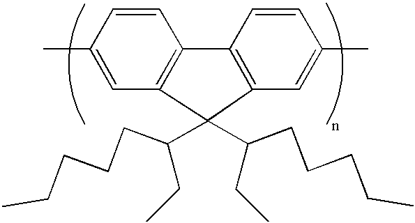
114. An example of a typical repeating unit of a polyfluorene is given below:
Figure US06555840-20030429-C00004
Following this, a dopant layer 116 to modify the charge transport properties of the polymer is printed onto the upper surface of the layer 114 and caused to diffuse into the latter to form a doped region 118 which, in this embodiment, extend throughout the thickness of the layer 114, but which may extend only partially through the thickness of the layer 114. Finally, a metal cathode 120 is provided on top of the layer 114.
Referring now to FIG. 7 of the drawings, an ITO-coated substrate 130 is covered with a layer 132 of a PPV polymer. Following this, a layer 134 of a PPV polymer precursor is deposited onto the layer 132. A dopant layer 136 is then printed onto a region of the layer 134 and caused to diffuse throughout the precursor polymer layer 134.
In this example, the dopant is chosen so that it interacts with the PPV polymer precursor. For example, the PPV polymer precursor may have structure shown below:
Figure US06555840-20030429-C00005
The above precursor polymer is soluble in, for example, water and methanol, and may be converted to a hydrophobic polymer by heating. The hydrophobic polymer is very insoluble in all solvents.
If the dye/dopant used for the layer 136 is hydrophilic, then it preferentially resides in the PPV polymer precursor layer 134 rather than migrating to the layer 132 which is not charged and which is hydrophobic. The resultant layer 134 with interacting dopant in region 138 is then cured to form a PPV polymer layer 140 which merges with the underlying PPV polymer layer 132. Following this, a further polymer layer 142 is provided over the layer 140. The layer 142 may likewise be formed of a PPV polymer or it may be a PBD layer or a blend of PPV and PBD. Finally, a metal cathode 144 is provided over the layer 142 to complete the structure.
Referring now to FIGS. 8 and 9 of the drawings, there is illustrated a structure comprising a substrate 150 coated with an ITO anode which in turn is coated with a hole transporting layer 154 including a localised region 156 of a hole-transporting dopant.
A layer 158 provided on the layer 154 includes a localised emissive dopant region 160 which is spaced from both the upper and lower major surfaces and from the edges of the layer 158. The region 160 can be provided within the layer 158 in a similar manner to the way in which the region 138 is provided within the layers 132, 140 and 142 in the embodiment of FIG. 7.
On top of the layer 158 is a layer 162 of an electron-transporting material including a localised electron-transporting dopant 164.
The layer 162 is topped by metal cathodes 166. One of the cathodes 166 contacts the region 164.
The region 156 may be formed in the layer 154 in an analogous manner to region 160 in layer 158. The layer 154 can be created in two steps. The first involves the formation of, for example, a hydrophilic precursor material layer into which hydrophilic dye/dopant will diffuse easily. Conversion of the hydrophilic precursor layer to a hydrophobic material then fixes the dye/dopant in region 156. A second layer of the same precursor material is then deposited and then converted to yield layer 154.
Clearly, the hydrophilic precursor material described above could be replaced by a hydrophobic precursor material, provided that a hydrophobic dye/dopant is used. Conversion could then yield a hydrophilic material that would trap the dye/dopant in region 156. A similar procedure is possible for layer 162 incorporating region 164. Generation of layer 162 would be carried out in two steps, the second involving a dye/dopant diffusion step.
In the above-described embodiments, ink-jet printing has been described for printing the required dopant/dye pattern on the layer into which it is to be diffused. However, it is possible mutatis mutandis to use any of the previously described alternative techniques, for example bubble-jet printing, screen printing, contact printing, aerosol spraying, electrostatic spraying, electrochemical deposition and photochemical deposition, for applying the dopant to be diffused.

Claims (12)

What is claimed is:
1. An organic opto-electronic structure comprising an organic charge-transport layer arrangement having: (a) an electron-transport region at one surface, (b) a hole-transport region at an opposite surface, and (c) at least one active region, wherein the or each active region is defined by a diffused region of the organic charge-transport layer arrangement into which at least one dopant has diffused, said diffused region extending only partly through the thickness of said layer arrangement,
wherein the organic charge-transport layer arrangement comprises a substantially uniform first organic charge-transport layer, a substantially uniform second organic charge-transport layer disposed on the first organic layer, an interface between said first and second organic layers, one of the organic layers defining the hole-transport region and the other organic layer defining the electron-transport region, and a plurality of active regions at the interface, wherein the or each active region is provided at the interface.
2. An opto-electronic structure according to claim 1, wherein the organic charge-transport layer arrangement is a polymer layer arrangement.
3. An opto-electronic structure according to claim 1, wherein said at least one dopant is a dye.
4. An opto-electronic structure according to claim 1, wherein the dopant is bound to the material of the layer into which it is diffused by a covalent bond, an electrostatic bond, a hydrophobic bonding interaction, a van der Waals' bonding interaction or a hydrogen bonding interaction.
5. An opto-electronic structure according to claim 4, wherein the dopant is bound by a covalent bond or an electrostatic bond.
6. An opto-electronic structure according to claim 1, further including a substrate upon which said layer arrangement is supported.
7. An opto-electronic structure according to claim 6, wherein the substrate is a flexible sheet of polymer or polymer/glass composite.
8. An opto-electronic structure according to claim 1, which is an electro-luminescent structure where the or each active region is a charge-carrier recombination/emitter region.
9. An opto-electronic structure according to claim 1, which is a photovoltaic structure wherein the or each active region to a light absorption/charge-carrier separation region.
10. An organic opto-electronic structure comprising an organic charge-transport layer arrangement having (a) an electron-transport region at one surface, (b) a hole-transport region at an opposite surface, and (c) at least one active region, wherein the or each active region is defined by a diffused region of the organic charge-transport layer arrangement into which at least one dopant has diffused, said diffused region extending only partly through the thickness of one of the said electron-transport region and hole-transport region, so as to form said layer arrangement,
wherein the organic charge-transport layer arrangement comprises a single organic layer having the electron-transport region and hole-transport region extending into the layer from opposite surfaces thereof, and said at least one active region is diffused into the layer from one of said surfaces.
11. An organic opto-electronic structure comprising an organic charge-transport layer arrangement having (a) an electron-transport region at one surface, (b) a hole-transport region at an opposite surface, and (c) at least one active region, wherein the or each active region is defined by a diffused region of the organic charge-transport layer arrangement into which at least one dopant has diffused, said diffused region extending only partly through the thickness of one of the said electron-transport region and hole-transport region, so as to form said layer arrangement,
wherein the structure is an electro-luminescent structure where the or each active region is a charge-carrier recombination/emitter region,
wherein a plurality of localised active regions are provided which can be individually addressed.
12. An organic opto-electronic structure comprising an organic charge-transport layer arrangement having (a) an electron-transport region at one surface, (b) a hole-transport region at an opposite surface, and (c) at least one active region, wherein the or each active region is defined by a diffused region of the organic charge-transport layer arrangement into which at least one dopant has diffused, said diffused region extending only partly through the thickness of one of the said electron-transport region and hole-transport region, so as to form said layer arrangement,
wherein the structure is a photovoltaic structure where the or each active region is a light absorption/charge-carrier separation region,
wherein a single active regions is provided which extends over the majority of the length and width of the organic charge-transport layer arrangement.
US09/504,557 1999-02-16 2000-02-15 Charge-transport structures Expired - Fee Related US6555840B1 (en)

Applications Claiming Priority (2)

Application Number Priority Date Filing Date Title
GB9903389A GB2347013A (en) 1999-02-16 1999-02-16 Charge-transport structures
GB9903389 1999-02-16

Publications (1)

Publication Number Publication Date
US6555840B1 true US6555840B1 (en) 2003-04-29

Family

ID=10847778

Family Applications (1)

Application Number Title Priority Date Filing Date
US09/504,557 Expired - Fee Related US6555840B1 (en) 1999-02-16 2000-02-15 Charge-transport structures

Country Status (4)

Country Link
US (1) US6555840B1 (en)
EP (1) EP1030383A3 (en)
JP (1) JP2000243562A (en)
GB (1) GB2347013A (en)

Cited By (86)

* Cited by examiner, † Cited by third party
Publication number Priority date Publication date Assignee Title
US20020164416A1 (en) * 1999-07-23 2002-11-07 Semiconductor Energy Laboratory Co., Ltd. EL display device and a method of manufacturing the same
US20020170090A1 (en) * 1997-02-18 2002-11-14 Washington State University Research Foundation Omega-3 fatty acid desaturase
US20030129790A1 (en) * 2001-11-09 2003-07-10 Semiconductor Energy Laboratory Co., Ltd. Light emitting apparatus and method for manufacturing the same
US20030178620A1 (en) * 2000-09-11 2003-09-25 Adolf Bernds Organic rectifier, circuit, rfid tag and use of an organic rectifier
US20030183817A1 (en) * 2000-09-01 2003-10-02 Adolf Bernds Organic field effect transistor, method for structuring an ofet and integrated circuit
US20030190767A1 (en) * 2000-07-07 2003-10-09 Adolf Bernds Method for the production and configuration of organic field-effect transistors (ofet)
US20040029310A1 (en) * 2000-08-18 2004-02-12 Adoft Bernds Organic field-effect transistor (ofet), a production method therefor, an integrated circut constructed from the same and their uses
US20040026689A1 (en) * 2000-08-18 2004-02-12 Adolf Bernds Encapsulated organic-electronic component, method for producing the same and use thereof
US20040026121A1 (en) * 2000-09-22 2004-02-12 Adolf Bernds Electrode and/or conductor track for organic components and production method thereof
US20040026690A1 (en) * 2000-09-13 2004-02-12 Adolf Bernds Organic memory, identification marker (rfid-tag) with organic memory and uses of an organic memory
US20040063267A1 (en) * 2000-12-08 2004-04-01 Adolf Bernds Organic field-effect transistor, method for structuring and ofet and integrated circuit
US20040092690A1 (en) * 2000-12-20 2004-05-13 Mark Giles Organic semiconductor, production method therefor and the use thereof
US20040096570A1 (en) * 2002-11-15 2004-05-20 Michael Weaver Structure and method of fabricating organic devices
US20040094771A1 (en) * 2001-03-26 2004-05-20 Adolf Bernds Device with at least two organic electronic components and method for producing the same
US20040124421A1 (en) * 2002-09-20 2004-07-01 Semiconductor Energy Laboratory Co., Ltd. Light-emitting device and manufacturing method thereof
US20040135497A1 (en) * 2002-05-29 2004-07-15 Kyung-Man Kim Organic electroluminescence display device and fabricating method of the same
US20040256467A1 (en) * 2001-10-18 2004-12-23 Wolfgang Clemens Electronic unit, circuit design for the same, and production method
US20040262599A1 (en) * 2001-06-01 2004-12-30 Adolf Bernds Organic field effect transistor, method for production and use thereof in the assembly of integrated circuits
US20050009231A1 (en) * 2003-06-03 2005-01-13 International Business Machines Corporation Melt-based patterning for electronic devices
US20050042548A1 (en) * 2001-04-04 2005-02-24 Hagen Klauk Self-aligned contact doping for organic field-effect transistors and method for fabricating the transistor
WO2005020332A2 (en) * 2003-08-22 2005-03-03 Itm Fuel Cells Ltd. Photovoltaic cell
US20050048803A1 (en) * 2001-10-16 2005-03-03 Erwann Guillet Insulator for an organic electronic component
US20050106507A1 (en) * 2002-03-21 2005-05-19 Adolf Bernds Device and method for laser structuring functional polymers and the use thereof
US20050214568A1 (en) * 2004-03-29 2005-09-29 Changchun Institute Of Applied Chemistry Chinese Academy Of Science White electroluminescent polymeric material & preparation thereof
US20050211972A1 (en) * 2001-12-11 2005-09-29 Siemens Aktiengesellschaft Organic field effect transistor with off-set threshold voltage and the use thereof
US20050224787A1 (en) * 2002-06-13 2005-10-13 Wolfgang Clemens Substrate for an organic field effect transistor, use of said substrate, method for increasing the charge carrier mobility, and organic field effect transistor (ofet)
US20050277240A1 (en) * 2002-03-21 2005-12-15 Walter Fix Logic components from organic field effect transistors
US20060006424A1 (en) * 2001-11-09 2006-01-12 Semiconductor Energy Laboratory Co., Ltd. Light emitting apparatus and method for manufacturing the same
US20060035423A1 (en) * 2002-11-19 2006-02-16 Walter Fix Organic electronic component comprising the same organic material for at least two functional layers
US20060079327A1 (en) * 2002-08-08 2006-04-13 Wolfgang Clemens Electronic device
US20060118778A1 (en) * 2002-11-05 2006-06-08 Wolfgang Clemens Organic electronic component with high-resolution structuring and method for the production thereof
US20060121625A1 (en) * 2002-11-14 2006-06-08 Wolfgang Clemens Measuring apparatus used for determining an analyte in a liquid sample, comprising polymer electronic components
US20060227531A1 (en) * 2005-04-06 2006-10-12 Au Optronics Corp. Electroluminescent displays
US20060237713A1 (en) * 2005-03-17 2006-10-26 Industrial Technology Research Institute Color organic electroluminescent display and method for fabricating the same
US20060250076A1 (en) * 2005-04-13 2006-11-09 Michael Hofmann Arrangement for an Organic Pin-Type Light-Emitting Diode and Method for Manufacturing
US20060273310A1 (en) * 2005-06-01 2006-12-07 Novaled Ag Light-Emitting Component with an Arrangement of Electrodes
US20060284170A1 (en) * 2005-05-27 2006-12-21 Novaled Ag Transparent Light-Emitting Component
US20070008019A1 (en) * 2003-09-03 2007-01-11 Wolfgang Clemens Mechanical control elements for organic polymer electronic devices
US20070017401A1 (en) * 2003-09-03 2007-01-25 Polyic Gmbh & Co. Kg Polymer mixtures for printed polymer electronic circuits
US20070030623A1 (en) * 2003-08-20 2007-02-08 Polyic Gmbh & Co. Kg Organic capacitor having a voltage-controlled capacitance
US20070046186A1 (en) * 2005-08-30 2007-03-01 Kim Eun-Ah Organic light emitting display and method of fabricating the same
US20070051946A1 (en) * 2005-07-01 2007-03-08 Novaled Ag Organic Light-Emitting Diodes and an Arrangement with Several Organic Light-Emitting Diodes
US7238961B2 (en) 2001-02-09 2007-07-03 Polyic Gmbh & Co. Kg Organic field effect transistor with a photostructured gate dielectric, method for the production and use thereof in organic electronics
US20070182316A1 (en) * 2006-02-01 2007-08-09 Mathew Mathai OLED with Area Defined Multicolor Emission Within a Single Lighting Element
US20070249076A1 (en) * 2000-11-02 2007-10-25 Masaya Ishida Organic electroluminescent device, method of manufacturing the same, and electronic apparatus
WO2008013427A1 (en) * 2006-07-27 2008-01-31 Lg Chem, Ltd. Organic tfts and method for fabricating the same
US20080061986A1 (en) * 2004-08-23 2008-03-13 Polylc Gmbh & Co. Kg External Package Capable of Being Radio-Tagged
US20080143250A1 (en) * 2006-12-14 2008-06-19 Novaled Ag Organisches Leuchtbauelement
US7414513B2 (en) 2002-08-23 2008-08-19 Polyic Gmbh & Co. Kg Organic component for overvoltage protection and associated circuit
US20080197343A1 (en) * 2004-12-10 2008-08-21 Robert Blache Organic Field Effect Transistor Gate
US20080204069A1 (en) * 2005-03-01 2008-08-28 Polyic Gmbh & Co. Kg Electronic Module With Organic Logic Circuit Elements
US20080203383A1 (en) * 2005-04-15 2008-08-28 Polyic Gmbh & Co. Kg Multi-Layer Composite Body Having an Electronic Function
US20080218315A1 (en) * 2004-12-10 2008-09-11 Markus Bohm Electronic Component Comprising a Modulator
US20090009072A1 (en) * 2005-12-23 2009-01-08 Philipp Wellmann Organic Light Emitting Device With a Plurality of Organic Electroluminescent Units Stacked Upon Each Other
US20090009071A1 (en) * 2005-12-21 2009-01-08 Sven Murano Organic Component
US7479670B2 (en) 2003-08-25 2009-01-20 Polyic Gmbh & Co Kg Organic electronic component with high resolution structuring, and method of the production thereof
US20090045728A1 (en) * 2005-12-23 2009-02-19 Sven Murano Electronic device with a layer structure of organic layers
US7507649B2 (en) 2004-10-07 2009-03-24 Novaled Ag Method for electrical doping a semiconductor material with Cesium
US20090108253A1 (en) * 2005-07-29 2009-04-30 Andreas Ullmann Electronic component
WO2006072022A3 (en) * 2004-12-30 2009-05-07 Du Pont Electronic device including a guest material within a layer and a process for forming the same
US7534034B2 (en) 2000-12-08 2009-05-19 Polyic Gmbh & Co. Kg Device for detecting at least one environmental influence
US7540978B2 (en) 2004-08-05 2009-06-02 Novaled Ag Use of an organic matrix material for producing an organic semiconductor material, organic semiconductor material and electronic component
US20090189147A1 (en) * 2004-01-14 2009-07-30 Walter Fix Organic transistor comprising a self-aligning gate electrode, and method for the production thereof
US20090230844A1 (en) * 2005-03-15 2009-09-17 Novaled Ag Light-emitting component
US20090237248A1 (en) * 2004-12-10 2009-09-24 Wolfgang Clemens Identification System
US20100051923A1 (en) * 2008-08-04 2010-03-04 Novaled Ag Organischer Feldeffekt Transistor
US20100065825A1 (en) * 2006-04-19 2010-03-18 Novaled Ag Light-Emitting Component
US20100065833A1 (en) * 2008-08-04 2010-03-18 Novaled Ag Organic field-effect transistor and circuit
CN1855569B (en) * 2005-03-25 2010-05-12 株式会社半导体能源研究所 Organic semiconductor device
US7724550B2 (en) 2004-12-23 2010-05-25 Polyic Gmbh & Co. Kg Organic rectifier
US20100135073A1 (en) * 2007-04-17 2010-06-03 Novaled Ag Organic electronic memory component, memory component arrangement and method for operating an organic electronic memory component
US20100214748A1 (en) * 2005-09-16 2010-08-26 Polyic Gmbh & Co. Kg Metal roof truss connector assembly
US20100295026A1 (en) * 2005-11-09 2010-11-25 Konica Minolta Holdings, Inc. Organic electroluminescent element, display device and lighting device
US7843342B2 (en) 2005-03-01 2010-11-30 Polyic Gmbh & Co. Kg Organic clock generator
US20100302532A1 (en) * 2007-03-29 2010-12-02 Avago Technologies Ecbu Ip (Singapore) Pte. Ltd. Photodetector having dark current correction
US7846838B2 (en) 2005-07-29 2010-12-07 Polyic Gmbh & Co. Kg Method for producing an electronic component
US20110081478A1 (en) * 2003-10-24 2011-04-07 National Institute Of Advanced Industrial Science And Technology Organic electroluminescent element and manufacturing method thereof
US7940340B2 (en) 2005-07-04 2011-05-10 Polyic Gmbh & Co. Kg Multilayer body with electrically controllable optically active systems of layers
US20110177641A1 (en) * 2010-01-20 2011-07-21 Universal Display Corporation Electroluminescent devices for lighting applications
US20110195201A1 (en) * 2010-02-06 2011-08-11 Tsinghua University Method for making a nano-optical antenna array
US8044517B2 (en) 2002-07-29 2011-10-25 Polyic Gmbh & Co. Kg Electronic component comprising predominantly organic functional materials and a method for the production thereof
CN102388475A (en) * 2009-03-20 2012-03-21 诺瓦莱德公开股份有限公司 Organic zener diode, electronic circuit, and method for operating an organic zener diode
US20130183782A1 (en) * 2010-07-21 2013-07-18 Sumitomo Chemical Company, Limited Method for producing organic el element
US8502200B2 (en) 2006-01-11 2013-08-06 Novaled Ag Electroluminescent light-emitting device comprising an arrangement of organic layers, and method for its production
US8653537B2 (en) 2004-08-13 2014-02-18 Novaled Ag Layer assembly for a light-emitting component
US20140263581A1 (en) * 2013-03-14 2014-09-18 Alpha Design Co., Ltd. Electronic component bonding method

Families Citing this family (17)

* Cited by examiner, † Cited by third party
Publication number Priority date Publication date Assignee Title
EP1143773A4 (en) * 1999-10-05 2007-02-21 Matsushita Electric Ind Co Ltd Luminescent device and method for manufacturing the same, and display and illuminator comprising the same
GB2374202A (en) * 2001-04-03 2002-10-09 Seiko Epson Corp Patterning method
JP4648594B2 (en) * 2001-09-07 2011-03-09 ブラザー工業株式会社 Manufacturing method of display device
DE60208913T2 (en) * 2001-09-11 2006-09-14 DuPont Teijin Films U.S., Ltd. Partnership, Wilmington HEAT-STABILIZED POLYETHYLENE NAPHTHALATE FILM FOR FLEXIBLE ELECTRONIC AND OPTO ELECTRONIC COMPONENTS
EP1338431A3 (en) * 2002-02-08 2003-10-01 Fuji Photo Film Co., Ltd. Visible image receiving material having surface hydrophilicity
AU2003263360A1 (en) 2002-09-03 2004-03-29 Cambridge Display Technology Limited Optical device
US6982179B2 (en) * 2002-11-15 2006-01-03 University Display Corporation Structure and method of fabricating organic devices
US7488540B2 (en) 2003-02-26 2009-02-10 Dai Nippon Printing Co., Ltd. Thin film laminate and luminescent element
US7655961B2 (en) * 2003-10-02 2010-02-02 Maxdem Incorporated Organic diodes and materials
WO2005048373A1 (en) * 2003-11-10 2005-05-26 E.I. Dupont De Nemours And Company Process for forming organic layers with a region including a guest material and organic electronic devices incorporating the same
US20050100657A1 (en) * 2003-11-10 2005-05-12 Macpherson Charles D. Organic material with a region including a guest material and organic electronic devices incorporating the same
KR101181820B1 (en) 2005-12-29 2012-09-11 삼성에스디아이 주식회사 Manufacturing method of solar cell
CN103733346A (en) * 2011-08-22 2014-04-16 住友化学株式会社 Organic thin film transistor
JP2013211534A (en) * 2012-02-28 2013-10-10 Sumitomo Chemical Co Ltd Method for manufacturing organic thin-film transistor and organic thin-film transistor
KR102378967B1 (en) * 2015-02-04 2022-03-24 바스프 에스이 Organic field-effect-transistors with low contact resistance
JP6943400B2 (en) * 2017-09-08 2021-09-29 株式会社アロマビット Method for manufacturing conductive polymer film
US11224284B2 (en) 2020-02-18 2022-01-18 Colgate-Palmolive Company Personal care system and fluid supply system thereof

Citations (15)

* Cited by examiner, † Cited by third party
Publication number Priority date Publication date Assignee Title
EP0554569A2 (en) 1991-12-30 1993-08-11 Eastman Kodak Company Efficient organic electroluminescent device of simplified construction
JPH06116552A (en) * 1992-10-02 1994-04-26 Sekisui Chem Co Ltd Organic electroluminescent element
EP0643549A1 (en) 1993-09-13 1995-03-15 Eastman Kodak Company White light emitting internal junction organic electroluminescent device
US5674597A (en) * 1994-07-14 1997-10-07 Sanyo Electric Co., Ltd. Organic electroluminescent elements
US5804836A (en) * 1995-04-05 1998-09-08 Uniax Corporation Smart polymer image processor
EP0892028A2 (en) 1997-07-16 1999-01-20 Seiko Epson Corporation Composition for an organic el element and method of manufacturing the organic el element
US5895692A (en) * 1993-12-28 1999-04-20 Casio Computer Co., Ltd. Manufacturing of organic electroluminescent device
US6023073A (en) * 1995-11-28 2000-02-08 International Business Machines Corp. Organic/inorganic alloys used to improve organic electroluminescent devices
US6048573A (en) * 1998-11-13 2000-04-11 Eastman Kodak Company Method of making an organic light-emitting device
US6075317A (en) * 1998-07-30 2000-06-13 Alliedsignal Inc. Electroluminescent device having increased brightness and resolution and method of fabrication
EP1017118A2 (en) * 1998-12-28 2000-07-05 Sharp Kabushiki Kaisha Organic electroluminescent element and production method thereof
US6117529A (en) * 1996-12-18 2000-09-12 Gunther Leising Organic electroluminescence devices and displays
EP1056141A2 (en) * 1999-05-25 2000-11-29 Matsushita Electric Industrial Co., Ltd. Electroluminescent device having a very thin emission layer
EP1083612A2 (en) * 1999-09-02 2001-03-14 Eastman Kodak Company Efficient electron-injection for organic electroluminescent devices
US6214151B1 (en) * 1999-11-05 2001-04-10 International Business Machines Corporation Thermal dye transfer process for preparing opto-electronic devices

Patent Citations (16)

* Cited by examiner, † Cited by third party
Publication number Priority date Publication date Assignee Title
EP0554569A2 (en) 1991-12-30 1993-08-11 Eastman Kodak Company Efficient organic electroluminescent device of simplified construction
JPH06116552A (en) * 1992-10-02 1994-04-26 Sekisui Chem Co Ltd Organic electroluminescent element
EP0643549A1 (en) 1993-09-13 1995-03-15 Eastman Kodak Company White light emitting internal junction organic electroluminescent device
US5895692A (en) * 1993-12-28 1999-04-20 Casio Computer Co., Ltd. Manufacturing of organic electroluminescent device
US5674597A (en) * 1994-07-14 1997-10-07 Sanyo Electric Co., Ltd. Organic electroluminescent elements
US5804836A (en) * 1995-04-05 1998-09-08 Uniax Corporation Smart polymer image processor
US6023073A (en) * 1995-11-28 2000-02-08 International Business Machines Corp. Organic/inorganic alloys used to improve organic electroluminescent devices
US6117529A (en) * 1996-12-18 2000-09-12 Gunther Leising Organic electroluminescence devices and displays
EP0892028A2 (en) 1997-07-16 1999-01-20 Seiko Epson Corporation Composition for an organic el element and method of manufacturing the organic el element
US6075317A (en) * 1998-07-30 2000-06-13 Alliedsignal Inc. Electroluminescent device having increased brightness and resolution and method of fabrication
US6048573A (en) * 1998-11-13 2000-04-11 Eastman Kodak Company Method of making an organic light-emitting device
EP1017118A2 (en) * 1998-12-28 2000-07-05 Sharp Kabushiki Kaisha Organic electroluminescent element and production method thereof
EP1056141A2 (en) * 1999-05-25 2000-11-29 Matsushita Electric Industrial Co., Ltd. Electroluminescent device having a very thin emission layer
EP1083612A2 (en) * 1999-09-02 2001-03-14 Eastman Kodak Company Efficient electron-injection for organic electroluminescent devices
US6278236B1 (en) * 1999-09-02 2001-08-21 Eastman Kodak Company Organic electroluminescent devices with electron-injecting layer having aluminum and alkali halide
US6214151B1 (en) * 1999-11-05 2001-04-10 International Business Machines Corporation Thermal dye transfer process for preparing opto-electronic devices

Non-Patent Citations (8)

* Cited by examiner, † Cited by third party
Title
European Search Report dated Jun. 5, 2002 in corresponding European Patent Application No. 00301196.2.
Fujii et al., "Organic Photovoltaic Cell With Donor-Acceptor Double Heterojunctions", Japanese Journal of Applied Physics, Publication Office Japanese Journal of Applied Physics, Tokyo, Japan, vol. 35, No. 11A, Nov. 1, 1996, pp. L1438-L-1441, XP000727737.
Granstroem et al., "Laminated Fabrication of Polymeric Photovoltaic Diodes", Nature, Macmillan Journals Ltd., London, GB, vol. 395, Sep. 17, 1998, pp. 257-260, XP000931238.
J.C. Sturm et al.; "Printing Approaches for Large-Area Color Organic LRD Displays"; SPIE, vol. 3797; Jul. 1999; pp. 266-273.
Pichler et al., "Field-Effect Transistors Based on Poly(P-Phenylene Vinylene) Doped by Ion Implantation", Journal of Applied Physics, American Institute of Physics, New York, US, vol. 77, No. 7, Apr. 1, 1995, pp. 3523-3527, XP000501594.
Pschenitzka et al.; "Three Color Organic Light-Emitting Diodes Patterned by Masked Dye Diffusion"; Appl. Phys. Lett., vol. 74, No. 13, Mar. 29, 1999, pp. 1913-1915.
Shoustikov et al., "Electroluminescence Color Tuning By Dye Doping in Organic Light-Emitting Diodes", IEEE Journal of Selected Topics in Quantum Electronics, IEEE Service Center, US, vol. 4, No. 1, 1998, pp. 3-13, XP000766104.
Tada et al.; "Three-Color Polymer Light-Emitting devices Patterned by Maskless Dye Diffusion onto Patterned Electrode"; Jpn. J. Appl. Phys., vol. 38; 1999; L.1143-1145.

Cited By (150)

* Cited by examiner, † Cited by third party
Publication number Priority date Publication date Assignee Title
US20020170090A1 (en) * 1997-02-18 2002-11-14 Washington State University Research Foundation Omega-3 fatty acid desaturase
US20040229392A1 (en) * 1999-07-23 2004-11-18 Semiconductor Energy Laboratory Co., Ltd. EL display device and a method of manufacturing the same
US7456037B2 (en) 1999-07-23 2008-11-25 Semiconductor Energy Laboratory Co., Ltd. EL display device and a method of manufacturing the same
US20020164416A1 (en) * 1999-07-23 2002-11-07 Semiconductor Energy Laboratory Co., Ltd. EL display device and a method of manufacturing the same
US6673643B2 (en) * 1999-07-23 2004-01-06 Semiconductor Energy Laboratory Co., Ltd. Method of manufacturing a EL display device
US6852583B2 (en) * 2000-07-07 2005-02-08 Siemens Aktiengesellschaft Method for the production and configuration of organic field-effect transistors (OFET)
US20030190767A1 (en) * 2000-07-07 2003-10-09 Adolf Bernds Method for the production and configuration of organic field-effect transistors (ofet)
US7875975B2 (en) 2000-08-18 2011-01-25 Polyic Gmbh & Co. Kg Organic integrated circuit completely encapsulated by multi-layered barrier and included in RFID tag
US20040026689A1 (en) * 2000-08-18 2004-02-12 Adolf Bernds Encapsulated organic-electronic component, method for producing the same and use thereof
US20040029310A1 (en) * 2000-08-18 2004-02-12 Adoft Bernds Organic field-effect transistor (ofet), a production method therefor, an integrated circut constructed from the same and their uses
US6960489B2 (en) 2000-09-01 2005-11-01 Siemens Aktiengesellschaft Method for structuring an OFET
US20030183817A1 (en) * 2000-09-01 2003-10-02 Adolf Bernds Organic field effect transistor, method for structuring an ofet and integrated circuit
US20030178620A1 (en) * 2000-09-11 2003-09-25 Adolf Bernds Organic rectifier, circuit, rfid tag and use of an organic rectifier
US20040026690A1 (en) * 2000-09-13 2004-02-12 Adolf Bernds Organic memory, identification marker (rfid-tag) with organic memory and uses of an organic memory
US6903958B2 (en) 2000-09-13 2005-06-07 Siemens Aktiengesellschaft Method of writing to an organic memory
US20040026121A1 (en) * 2000-09-22 2004-02-12 Adolf Bernds Electrode and/or conductor track for organic components and production method thereof
US20100190281A1 (en) * 2000-11-02 2010-07-29 Seiko Epson Corporation Organic electroluminescent device, method of manufacturing the same, and electronic apparatus
US20070249076A1 (en) * 2000-11-02 2007-10-25 Masaya Ishida Organic electroluminescent device, method of manufacturing the same, and electronic apparatus
US7718453B2 (en) * 2000-11-02 2010-05-18 Seiko Epson Corporation Organic electroluminescent device, method of manufacturing the same, and electronic apparatus
US7951627B2 (en) 2000-11-02 2011-05-31 Seiko Epson Corporation Organic electroluminescent device, method of manufacturing the same, and electronic apparatus
US7534034B2 (en) 2000-12-08 2009-05-19 Polyic Gmbh & Co. Kg Device for detecting at least one environmental influence
US7229868B2 (en) * 2000-12-08 2007-06-12 Polyic Gmbh & Co. Kg Organic field-effect transistor, method for structuring an OFET and integrated circuit
US20040063267A1 (en) * 2000-12-08 2004-04-01 Adolf Bernds Organic field-effect transistor, method for structuring and ofet and integrated circuit
US20040092690A1 (en) * 2000-12-20 2004-05-13 Mark Giles Organic semiconductor, production method therefor and the use thereof
US7238961B2 (en) 2001-02-09 2007-07-03 Polyic Gmbh & Co. Kg Organic field effect transistor with a photostructured gate dielectric, method for the production and use thereof in organic electronics
US20040094771A1 (en) * 2001-03-26 2004-05-20 Adolf Bernds Device with at least two organic electronic components and method for producing the same
US20050042548A1 (en) * 2001-04-04 2005-02-24 Hagen Klauk Self-aligned contact doping for organic field-effect transistors and method for fabricating the transistor
US20040262599A1 (en) * 2001-06-01 2004-12-30 Adolf Bernds Organic field effect transistor, method for production and use thereof in the assembly of integrated circuits
US20050048803A1 (en) * 2001-10-16 2005-03-03 Erwann Guillet Insulator for an organic electronic component
US7298023B2 (en) 2001-10-16 2007-11-20 Polyic Gmbh & Co. Kg Electronic device with organic insulator
US7483275B2 (en) 2001-10-18 2009-01-27 Polyic Gmbh & Co. Kg Electronic unit, circuit design for the same, and production method
US20040256467A1 (en) * 2001-10-18 2004-12-23 Wolfgang Clemens Electronic unit, circuit design for the same, and production method
US20110180801A1 (en) * 2001-11-09 2011-07-28 Semiconductor Energy Laboratory Co., Ltd. Light emitting apparatus and method for manufacturing the same
US7432529B2 (en) 2001-11-09 2008-10-07 Semiconductor Energy Laboratory Co., Ltd. Light emitting apparatus and method for manufacturing the same
US10516010B2 (en) 2001-11-09 2019-12-24 Semiconductor Energy Laboratory Co., Ltd. Light emitting apparatus and method for manufacturing the same
US20060006424A1 (en) * 2001-11-09 2006-01-12 Semiconductor Energy Laboratory Co., Ltd. Light emitting apparatus and method for manufacturing the same
US7709846B2 (en) 2001-11-09 2010-05-04 Semiconductor Energy Laboratory Co., Ltd. Light emitting apparatus and method for manufacturing the same
US20050224820A1 (en) * 2001-11-09 2005-10-13 Semiconductor Energy Laboratory Co., Ltd. Light emitting apparatus and method for manufacturing the same
US20090256467A1 (en) * 2001-11-09 2009-10-15 Semiconductor Energy Laboratory Co., Ltd. Light emitting apparatus and method for manufacturing the same
US7042024B2 (en) * 2001-11-09 2006-05-09 Semiconductor Energy Laboratory Co., Ltd. Light emitting apparatus and method for manufacturing the same
US7442963B2 (en) 2001-11-09 2008-10-28 Semiconductor Energy Laboratory Co., Ltd. Light emitting apparatus and method for manufacturing the same
US6903377B2 (en) 2001-11-09 2005-06-07 Semiconductor Energy Laboratory Co., Ltd. Light emitting apparatus and method for manufacturing the same
US20030129790A1 (en) * 2001-11-09 2003-07-10 Semiconductor Energy Laboratory Co., Ltd. Light emitting apparatus and method for manufacturing the same
US8785949B2 (en) 2001-11-09 2014-07-22 Semiconductor Energy Laboratory Co., Ltd. Light emitting apparatus and method for manufacturing the same
US8174029B2 (en) 2001-11-09 2012-05-08 Semiconductor Energy Laboratory Co., Ltd. Light emitting apparatus and method for manufacturing the same
US7939835B2 (en) 2001-11-09 2011-05-10 Semiconductor Energy Laboratory Co., Ltd. Light emitting apparatus and method for manufacturing the same
US20100201662A1 (en) * 2001-11-09 2010-08-12 Semiconductor Energy Laboratory Co., Ltd. Light emitting apparatus and method for manufacturing the same
US7064345B2 (en) 2001-12-11 2006-06-20 Siemens Aktiengesellschaft Organic field effect transistor with off-set threshold voltage and the use thereof
US20050211972A1 (en) * 2001-12-11 2005-09-29 Siemens Aktiengesellschaft Organic field effect transistor with off-set threshold voltage and the use thereof
US20050106507A1 (en) * 2002-03-21 2005-05-19 Adolf Bernds Device and method for laser structuring functional polymers and the use thereof
US7223995B2 (en) 2002-03-21 2007-05-29 Polyic Gmbh & Co. Kg Logic components comprising organic field effect transistors
US20050277240A1 (en) * 2002-03-21 2005-12-15 Walter Fix Logic components from organic field effect transistors
US7012280B2 (en) * 2002-05-29 2006-03-14 Lg.Philips Lcd Co., Ltd. Organic electroluminescence display device fabricating method of the same
US20040135497A1 (en) * 2002-05-29 2004-07-15 Kyung-Man Kim Organic electroluminescence display device and fabricating method of the same
US20050224787A1 (en) * 2002-06-13 2005-10-13 Wolfgang Clemens Substrate for an organic field effect transistor, use of said substrate, method for increasing the charge carrier mobility, and organic field effect transistor (ofet)
US7709865B2 (en) 2002-06-13 2010-05-04 Polyic Gmbh & Co. Kg Substrate for an organic field effect transistor, use of said substrate, method of increasing the charge carrier mobility, and organic field effect transistor (OFET)
US8044517B2 (en) 2002-07-29 2011-10-25 Polyic Gmbh & Co. Kg Electronic component comprising predominantly organic functional materials and a method for the production thereof
US20060079327A1 (en) * 2002-08-08 2006-04-13 Wolfgang Clemens Electronic device
US7414513B2 (en) 2002-08-23 2008-08-19 Polyic Gmbh & Co. Kg Organic component for overvoltage protection and associated circuit
US20040124421A1 (en) * 2002-09-20 2004-07-01 Semiconductor Energy Laboratory Co., Ltd. Light-emitting device and manufacturing method thereof
US20060118778A1 (en) * 2002-11-05 2006-06-08 Wolfgang Clemens Organic electronic component with high-resolution structuring and method for the production thereof
US7641857B2 (en) 2002-11-14 2010-01-05 Polyic Gmbh & Co. Kg Measuring apparatus used for determining an analyte in a liquid sample, comprising polymer electronic components
US20060121625A1 (en) * 2002-11-14 2006-06-08 Wolfgang Clemens Measuring apparatus used for determining an analyte in a liquid sample, comprising polymer electronic components
US20040096570A1 (en) * 2002-11-15 2004-05-20 Michael Weaver Structure and method of fabricating organic devices
US20060035423A1 (en) * 2002-11-19 2006-02-16 Walter Fix Organic electronic component comprising the same organic material for at least two functional layers
US7282430B2 (en) * 2003-06-03 2007-10-16 International Business Machines Corporation Melt-based patterning for electronic devices
US20050009231A1 (en) * 2003-06-03 2005-01-13 International Business Machines Corporation Melt-based patterning for electronic devices
US20070030623A1 (en) * 2003-08-20 2007-02-08 Polyic Gmbh & Co. Kg Organic capacitor having a voltage-controlled capacitance
EA009476B1 (en) * 2003-08-22 2008-02-28 Ай Ти Эм ФЬЮЭЛ СЕЛЛЗ ЛТД. Photovoltaic cell
WO2005020332A2 (en) * 2003-08-22 2005-03-03 Itm Fuel Cells Ltd. Photovoltaic cell
WO2005020332A3 (en) * 2003-08-22 2005-08-18 Itm Fuel Cells Ltd Photovoltaic cell
US20110088757A1 (en) * 2003-08-22 2011-04-21 Donald James Highgate Photovoltaic Cell
US7479670B2 (en) 2003-08-25 2009-01-20 Polyic Gmbh & Co Kg Organic electronic component with high resolution structuring, and method of the production thereof
US20070008019A1 (en) * 2003-09-03 2007-01-11 Wolfgang Clemens Mechanical control elements for organic polymer electronic devices
US20070017401A1 (en) * 2003-09-03 2007-01-25 Polyic Gmbh & Co. Kg Polymer mixtures for printed polymer electronic circuits
US7576294B2 (en) 2003-09-03 2009-08-18 Polyic Gmbh & Co. Kg Mechanical control elements for organic polymer electronic devices
US7678857B2 (en) 2003-09-03 2010-03-16 Polyic Gmbh & Co. Kg Polymer mixtures for printed polymer electronic circuits
US20110081478A1 (en) * 2003-10-24 2011-04-07 National Institute Of Advanced Industrial Science And Technology Organic electroluminescent element and manufacturing method thereof
US20090189147A1 (en) * 2004-01-14 2009-07-30 Walter Fix Organic transistor comprising a self-aligning gate electrode, and method for the production thereof
US20050214568A1 (en) * 2004-03-29 2005-09-29 Changchun Institute Of Applied Chemistry Chinese Academy Of Science White electroluminescent polymeric material & preparation thereof
US7579091B2 (en) * 2004-03-29 2009-08-25 Changchun Institute Of Applied Chemistry Chinese Academy Of Science White electroluminescent polymeric material and preparation thereof
US7540978B2 (en) 2004-08-05 2009-06-02 Novaled Ag Use of an organic matrix material for producing an organic semiconductor material, organic semiconductor material and electronic component
US8653537B2 (en) 2004-08-13 2014-02-18 Novaled Ag Layer assembly for a light-emitting component
US7847695B2 (en) 2004-08-23 2010-12-07 Polyic Gmbh & Co. Kg External package capable of being radio-tagged
US20080061986A1 (en) * 2004-08-23 2008-03-13 Polylc Gmbh & Co. Kg External Package Capable of Being Radio-Tagged
US7507649B2 (en) 2004-10-07 2009-03-24 Novaled Ag Method for electrical doping a semiconductor material with Cesium
US20080197343A1 (en) * 2004-12-10 2008-08-21 Robert Blache Organic Field Effect Transistor Gate
US20090237248A1 (en) * 2004-12-10 2009-09-24 Wolfgang Clemens Identification System
US20080218315A1 (en) * 2004-12-10 2008-09-11 Markus Bohm Electronic Component Comprising a Modulator
US7940159B2 (en) 2004-12-10 2011-05-10 Polyic Gmbh & Co. Kg Identification system
US7724550B2 (en) 2004-12-23 2010-05-25 Polyic Gmbh & Co. Kg Organic rectifier
WO2006072022A3 (en) * 2004-12-30 2009-05-07 Du Pont Electronic device including a guest material within a layer and a process for forming the same
CN101438382B (en) * 2004-12-30 2011-07-13 E.I.内穆尔杜邦公司 Electronic device including a guest material within a layer and a process for forming the same
US20080204069A1 (en) * 2005-03-01 2008-08-28 Polyic Gmbh & Co. Kg Electronic Module With Organic Logic Circuit Elements
US7843342B2 (en) 2005-03-01 2010-11-30 Polyic Gmbh & Co. Kg Organic clock generator
US7589553B2 (en) 2005-03-01 2009-09-15 Polyic Gmbh & Co. Kg Electronic module with organic logic circuit elements
US7986090B2 (en) 2005-03-15 2011-07-26 Novaled Ag Light-emitting component
US20090230844A1 (en) * 2005-03-15 2009-09-17 Novaled Ag Light-emitting component
US7619243B2 (en) * 2005-03-17 2009-11-17 Industrial Technology Research Institute Color organic electroluminescent display and method for fabricating the same
US20060237713A1 (en) * 2005-03-17 2006-10-26 Industrial Technology Research Institute Color organic electroluminescent display and method for fabricating the same
CN1855569B (en) * 2005-03-25 2010-05-12 株式会社半导体能源研究所 Organic semiconductor device
US20060227531A1 (en) * 2005-04-06 2006-10-12 Au Optronics Corp. Electroluminescent displays
CN101872843B (en) * 2005-04-13 2012-07-04 诺瓦莱德公开股份有限公司 Device for organic light emitting diode of pin-type and method for its manufacture
US20060250076A1 (en) * 2005-04-13 2006-11-09 Michael Hofmann Arrangement for an Organic Pin-Type Light-Emitting Diode and Method for Manufacturing
US7911129B2 (en) 2005-04-13 2011-03-22 Novaled Ag Arrangement for an organic pin-type light-emitting diode and method for manufacturing
US7812343B2 (en) 2005-04-15 2010-10-12 Polyic Gmbh & Co. Kg Multilayer composite body having an electronic function
US20080203383A1 (en) * 2005-04-15 2008-08-28 Polyic Gmbh & Co. Kg Multi-Layer Composite Body Having an Electronic Function
US20060284170A1 (en) * 2005-05-27 2006-12-21 Novaled Ag Transparent Light-Emitting Component
US7598519B2 (en) 2005-05-27 2009-10-06 Novaled Ag Transparent light-emitting component
US20060273310A1 (en) * 2005-06-01 2006-12-07 Novaled Ag Light-Emitting Component with an Arrangement of Electrodes
US20070051946A1 (en) * 2005-07-01 2007-03-08 Novaled Ag Organic Light-Emitting Diodes and an Arrangement with Several Organic Light-Emitting Diodes
US7940340B2 (en) 2005-07-04 2011-05-10 Polyic Gmbh & Co. Kg Multilayer body with electrically controllable optically active systems of layers
US7846838B2 (en) 2005-07-29 2010-12-07 Polyic Gmbh & Co. Kg Method for producing an electronic component
US20090108253A1 (en) * 2005-07-29 2009-04-30 Andreas Ullmann Electronic component
US20070046186A1 (en) * 2005-08-30 2007-03-01 Kim Eun-Ah Organic light emitting display and method of fabricating the same
US7839077B2 (en) * 2005-08-30 2010-11-23 Samsung Mobile Display Co., Ltd. Organic light emitting display and method of fabricating the same
US8315061B2 (en) 2005-09-16 2012-11-20 Polyic Gmbh & Co. Kg Electronic circuit with elongated strip layer and method for the manufacture of the same
US20100214748A1 (en) * 2005-09-16 2010-08-26 Polyic Gmbh & Co. Kg Metal roof truss connector assembly
US9082996B2 (en) 2005-11-09 2015-07-14 Konica Minolta, Inc. Organic electroluminescent element, display device and lighting device
US8053765B2 (en) * 2005-11-09 2011-11-08 Konica Minolta Holdings, Inc. Organic electroluminescent element, display device and lighting device
US20100295026A1 (en) * 2005-11-09 2010-11-25 Konica Minolta Holdings, Inc. Organic electroluminescent element, display device and lighting device
US9112175B2 (en) 2005-12-21 2015-08-18 Novaled Ag Organic component
US20090009071A1 (en) * 2005-12-21 2009-01-08 Sven Murano Organic Component
US20090045728A1 (en) * 2005-12-23 2009-02-19 Sven Murano Electronic device with a layer structure of organic layers
US7830089B2 (en) 2005-12-23 2010-11-09 Novaled Ag Electronic device with a layer structure of organic layers
US20090009072A1 (en) * 2005-12-23 2009-01-08 Philipp Wellmann Organic Light Emitting Device With a Plurality of Organic Electroluminescent Units Stacked Upon Each Other
US8502200B2 (en) 2006-01-11 2013-08-06 Novaled Ag Electroluminescent light-emitting device comprising an arrangement of organic layers, and method for its production
US20070182316A1 (en) * 2006-02-01 2007-08-09 Mathew Mathai OLED with Area Defined Multicolor Emission Within a Single Lighting Element
US20100065825A1 (en) * 2006-04-19 2010-03-18 Novaled Ag Light-Emitting Component
US8569743B2 (en) 2006-04-19 2013-10-29 Novaled Ag Light-emitting component
WO2008013427A1 (en) * 2006-07-27 2008-01-31 Lg Chem, Ltd. Organic tfts and method for fabricating the same
US20080143250A1 (en) * 2006-12-14 2008-06-19 Novaled Ag Organisches Leuchtbauelement
US7879641B2 (en) * 2007-03-29 2011-02-01 Avago Technologies Ecbu Ip (Singapore) Pte. Ltd. Photodetector having dark current correction
US20100302532A1 (en) * 2007-03-29 2010-12-02 Avago Technologies Ecbu Ip (Singapore) Pte. Ltd. Photodetector having dark current correction
US8254165B2 (en) 2007-04-17 2012-08-28 Novaled Ag Organic electronic memory component, memory component arrangement and method for operating an organic electronic memory component
US20100135073A1 (en) * 2007-04-17 2010-06-03 Novaled Ag Organic electronic memory component, memory component arrangement and method for operating an organic electronic memory component
US8071976B2 (en) * 2008-08-04 2011-12-06 Novaled Ag Organic field-effect transistor and circuit
US20100051923A1 (en) * 2008-08-04 2010-03-04 Novaled Ag Organischer Feldeffekt Transistor
US8212241B2 (en) 2008-08-04 2012-07-03 Novaled Ag Organic field-effect transistor
US20100065833A1 (en) * 2008-08-04 2010-03-18 Novaled Ag Organic field-effect transistor and circuit
CN102388475A (en) * 2009-03-20 2012-03-21 诺瓦莱德公开股份有限公司 Organic zener diode, electronic circuit, and method for operating an organic zener diode
CN102388475B (en) * 2009-03-20 2016-06-29 诺瓦莱德公开股份有限公司 Organic Zener diode, electronic circuit and the method for running organic Zener diode
US20110177641A1 (en) * 2010-01-20 2011-07-21 Universal Display Corporation Electroluminescent devices for lighting applications
US9054344B2 (en) 2010-01-20 2015-06-09 Universal Display Corporation Electroluminescent devices for lighting applications
US8288187B2 (en) 2010-01-20 2012-10-16 Universal Display Corporation Electroluminescent devices for lighting applications
US20110195201A1 (en) * 2010-02-06 2011-08-11 Tsinghua University Method for making a nano-optical antenna array
US9276237B2 (en) * 2010-07-21 2016-03-01 Sumitomo Chemical Company, Limited Method for producing organic EL element
US20130183782A1 (en) * 2010-07-21 2013-07-18 Sumitomo Chemical Company, Limited Method for producing organic el element
US8915418B2 (en) * 2013-03-14 2014-12-23 Tadatomo Suga Electronic component bonding method
US20140263581A1 (en) * 2013-03-14 2014-09-18 Alpha Design Co., Ltd. Electronic component bonding method

Also Published As

Publication number Publication date
GB9903389D0 (en) 1999-04-07
GB2347013A (en) 2000-08-23
EP1030383A3 (en) 2002-07-17
EP1030383A2 (en) 2000-08-23
JP2000243562A (en) 2000-09-08

Similar Documents

Publication Publication Date Title
US6555840B1 (en) Charge-transport structures
US7629061B2 (en) Heterostructure devices using cross-linkable polymers
EP1518281B8 (en) Buffer layers for organic electroluminescent devices and methods of manufacture and use
Forrest Active optoelectronics using thin-film organic semiconductors
TWI355862B (en) Methods for producing full-color organic electrolu
US9054317B2 (en) Multilayer organic device
US6372154B1 (en) Luminescent ink for printing of organic luminescent devices
EP1816690B1 (en) OLED with area defined multicolor emission within a single lighting element
KR101366655B1 (en) Neutralized anode buffer layers to improve processing and performances of organic electronic devices
US7407716B2 (en) Light emitting devices with multiple light emitting layers to achieve broad spectrum
TW200541385A (en) Printing of organic electronic devices
JP2007027763A (en) Organic light emitting diode device having multiple stacked layers, and organic light emitting diode device
CN102132441A (en) Method of manufacturing a display
US7452613B2 (en) White organic electroluminescent device
US20050156176A1 (en) Method for printing organic devices
US20050276910A1 (en) Post processing of films to improve film quality
CN1926698B (en) Deposition of conducting polymers
EP1520306A2 (en) Electroluminescent device with a color filter
CN101087012B (en) Organic EL component

Legal Events

Date Code Title Description
AS Assignment

Owner name: SHARP KABUSHIKI KAISHA, JAPAN

Free format text: ASSIGNMENT OF ASSIGNORS INTEREST;ASSIGNORS:HUDSON, ANDREW JAMES;ANDERSON, SALLY;WEAVER, MICHAEL STUART;AND OTHERS;REEL/FRAME:010994/0380

Effective date: 20000803

FEPP Fee payment procedure

Free format text: PAYOR NUMBER ASSIGNED (ORIGINAL EVENT CODE: ASPN); ENTITY STATUS OF PATENT OWNER: LARGE ENTITY

FPAY Fee payment

Year of fee payment: 4

REMI Maintenance fee reminder mailed
LAPS Lapse for failure to pay maintenance fees
STCH Information on status: patent discontinuation

Free format text: PATENT EXPIRED DUE TO NONPAYMENT OF MAINTENANCE FEES UNDER 37 CFR 1.362

FP Lapsed due to failure to pay maintenance fee

Effective date: 20110429