US6556703B1 - Scanning electron microscope system and method of manufacturing an integrated circuit - Google Patents
Scanning electron microscope system and method of manufacturing an integrated circuit Download PDFInfo
- Publication number
- US6556703B1 US6556703B1 US08/957,122 US95712297A US6556703B1 US 6556703 B1 US6556703 B1 US 6556703B1 US 95712297 A US95712297 A US 95712297A US 6556703 B1 US6556703 B1 US 6556703B1
- Authority
- US
- United States
- Prior art keywords
- signal
- wafer
- correlation
- auto
- substrate
- Prior art date
- Legal status (The legal status is an assumption and is not a legal conclusion. Google has not performed a legal analysis and makes no representation as to the accuracy of the status listed.)
- Expired - Lifetime
Links
Images


Classifications
-
- G—PHYSICS
- G01—MEASURING; TESTING
- G01N—INVESTIGATING OR ANALYSING MATERIALS BY DETERMINING THEIR CHEMICAL OR PHYSICAL PROPERTIES
- G01N23/00—Investigating or analysing materials by the use of wave or particle radiation, e.g. X-rays or neutrons, not covered by groups G01N3/00 – G01N17/00, G01N21/00 or G01N22/00
- G01N23/22—Investigating or analysing materials by the use of wave or particle radiation, e.g. X-rays or neutrons, not covered by groups G01N3/00 – G01N17/00, G01N21/00 or G01N22/00 by measuring secondary emission from the material
- G01N23/225—Investigating or analysing materials by the use of wave or particle radiation, e.g. X-rays or neutrons, not covered by groups G01N3/00 – G01N17/00, G01N21/00 or G01N22/00 by measuring secondary emission from the material using electron or ion
- G01N23/2251—Investigating or analysing materials by the use of wave or particle radiation, e.g. X-rays or neutrons, not covered by groups G01N3/00 – G01N17/00, G01N21/00 or G01N22/00 by measuring secondary emission from the material using electron or ion using incident electron beams, e.g. scanning electron microscopy [SEM]
Definitions
- the present invention relates generally to scanning electron microscopes and, more particularly, to a scanning electronic microscope processor for analyzing semiconductor devices and a method of manufacturing an integrated circuit.
- SEM scanning electron microscopes
- cross-sections of wafers are performed to assess the quality of a wafer. Although this process may be useful, the process is destructive and time consuming. As a result, a small number of wafers are selected for testing.
- An alternative approach is to perform electrical tests at the end of wafer processing to determine if deficiencies exist and assess the quality of the semiconductor devices formed on the wafer. Although deficiencies may be found, the defects are not detected until the end of wafer processing. As a result, problems in the manufacturing process or with the equipment used during manufacturing may not be detected. Numerous defective wafers may be produced before problems with the manufacturing or measurement process can be corrected.
- the present invention provides a method and system for analyzing the intensity profiles of a wafer including the step of scanning the wafer to produce a scanned signal.
- the scanned signal is preprocessed and compared to a reference signal to assess the wafer.
- the present invention is also directed to a method of manufacturing a wafer using the above method and system.
- FIG. 1 is a block diagram of scanning electron microscope system 100 according to the present invention.
- FIGS. 2-5 are flow chart diagrams for illustrating the operation of the scanning electron microscope system 100 shown in FIG. 1;
- FIGS. 6-22 are graphs illustrating the operation of the scanning electron microscope system 100 .
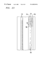
- FIG. 23 is a SEM picture of a metal line on a wafer illustrating an alternative embodiment.
- the present invention is directed to a scanning electron microscope system that measures and analyzes the surface topology of a wafer during the manufacturing process.
- the present invention analyzes the shape of the scanned features.
- the surface topology is measured using a scanning electron microscope which produces intensity values in an array, an intensity profile.
- the intensity profile may then be processed using signal processing techniques and compared to standard waveforms from, for example, a standardized wafer which has been processed in the same manner.
- the standard waveforms are waveforms representing known shapes of scanned features. Differences and errors in the wafer are manifested in the measured topology and may be detected by the comparison. Errors in the measurement, i.e. focus and sharpness, by the SEM may also be determined.
- the measured intensity topology can not be matched to the standard waveforms, it may be stored for further analysis. As a result, process monitoring may be improved and fatal errors in the wafers may be detected before further processing. Further, the above process may be implemented without adding additional steps to the manufacturing process because scanning electron microscopes are already used during processing.
- FIG. 1 is a scanning electron microscope (SEM) system 100 .
- the SEM system 100 includes a scanning electron microscope (SEM) 150 for scanning a wafer 120 or a substrate having a surface feature and producing a wafer waveform signal y i (t).
- An exemplary wafer waveform signal y i (t) for a resist line is shown in FIG. 6 .
- the SEM 150 is, for example, Model 8820 available from Hitachi, 3100 North 1 st Street, San Jose, Calif. 95134 USA.
- the SEM 150 is coupled to a processor 110 .
- the processor 110 receives the wafer waveform signal y i (t) and detects errors and deficiencies in the wafer 120 by analyzing the wafer waveform signal y i (t). In addition, the processor 110 may detect deviations in the manufacturing process such as variations between tools. This process may be performed in-line during the manufacturing process. “In-line during the manufacturing process” means during the process of forming circuitry on the wafer 120 . Consequently, process errors and degraded quality in, for example, the lithography and etching processes may be detected before manufacture of the devices is completed. Measurement errors, such as charging, may also be detected. Measurement errors can cause unnecessary reworks or scrap.
- adjustments may be made in the manufacturing line to correct, for example, tool drift and tool-to-tool matching for SEMs, steppers, and etchers.
- This allows problems such as SEM charging, stepper out of focus, and over etch errors to be detected and corrected.
- defective wafers may be detected and removed prior to further processing.
- wafer characterization may be performed to determine profile degradation across a wafer. As a result, the cost of the manufacturing process may be decreased while increasing the quality of the wafers 120 produced.
- the SEM system 100 also includes a database 125 for storing reference data.
- the SEM system 100 may also include a tool or tools 130 that may be automatically or manually adjusted in response to the analysis performed by the SEM system 100 .
- the components shown in FIG. 1 may be combined into one or more components and may be implemented in hardware or software. The operation of SEM system 100 is described below with reference to FIGS. 2-5. In addition, the process shown in FIGS. 2-5 is illustrated using the example shown in FIGS. 6-22.
- the SEM 150 acquires the wafer waveform signal y i (t).
- An exemplary wafer waveform signal y i (t) for a charged resist line is shown in FIG. 7 .
- FIG. 8 is a diagram corresponding to a portion of the waveform shown in FIG. 7 .
- the processor 110 generates a processed waveform signal p 22 (t) from the wafer waveform signal y i (t) by implementing an auto-correlation operation.
- Step 205 is described in greater detail below with reference to FIG. 3 .
- the processor 110 processes the wafer waveform signal y i (t) using, for example, equation (1) below to produce a converted waveform signal Y i (jw).
- FIG. 9 is an exemplary converted waveform Y i (jw) for the wafer waveform signal y i (t) shown in FIG. 8 .
- the converted waveform signal Y i (jw) is filtered using a low pass filter as is shown in equation (2) below to produce a filtered waveform signal Y f (jw).
- the filter implemented by equation (2) may pass a quarter (1 ⁇ 4) or less of the components of the converted waveform signal Y i (jw). The high frequency components are removed to reduce the systematic noise in the wafer waveform signal y i (t). Other filters may be used.
- FIG. 10 is the filtered waveform signal Y f (jw) corresponding to the converted waveform signal Y i (jw) shown in FIG. 9 .
- an auto-correlation operation is performed to produce a wafer auto-correlation signal R 22 (jw) from the filtered waveform signal Y f (jw) using equation (3) below.
- Equation (3) the “*” indicates a complex conjugate.
- An exemplary wafer auto-correlation signal R 22 (jw) is shown in FIG. 11 .
- an inverse transform is performed to produce a transformed signal r 22 (t) using equation (4) below.
- r 22 ⁇ ( t ) F - 1 ⁇ [ R 22 ⁇ ( j ⁇ ⁇ w ) ] N ( 4 )
- N is the total number of pixels that would be used for display i ng the waveform or the total number of input quantities (samples).
- N is the total number of pixels that would be used for display i ng the waveform or the total number of input quantities (samples).
- an exemplary transformed signal r 22 (t) is shown in FIG. 12 .
- the maximum value MAX 22 of the transformed signal r 22 (t) is determined at a phase or lag equal to zero (0) as is shown in equation (5) below.
- the transformed signal r 22 (t) is normalized according to equation (6) below to produce the auto-correlation waveform signal p 22 (t).
- P 22 ⁇ ( t ) r 22 ⁇ ( t ) Max 22 ( 6 )
- An exemplary auto-correlation signal p 22 (t) is shown in FIG. 13 where the transformed signal r 22 (t) is normalized.
- the result is a function of probability densities for a lag of t. This is shown for completeness, but is not necessary for further processing.
- the maximum value MAX 22 is, for example, 332.164.
- the wafer waveform signal y i (t) is compared to a standard waveform signal x i (t) using the auto-correlation signal p 22 (t).
- the standard waveform signal x i (t) is used as a bench mark to determine whether other wafers 120 have deficiencies and satisfy quality standards and to detect variations in the manufacturing process.
- the standard waveform signal x i (t) is derived from a scan of a standard wafer (not shown).
- the standard wafer is a wafer that satisfies the desired manufacturing criteria for producing the wafer 120 . In other words, the wafer 120 is acceptable if the wafer 120 is within a specified range of the standard wafer.
- the process for deriving the standard auto-correlation signal p 11 is the same as the process for producing the wafer auto-correlation signal p 22 except the process is performed on a scanned signal rather than standard wafer.
- the process for deriving the standard auto-correlation signal p 11 is shown in FIG. 4. A description of FIG. 4 is omitted for the sake of brevity.
- FIGS. 14-19 are exemplary waveforms corresponding to the process steps shown in FIG. 4 .
- FIG. 14 is an exemplary standard waveform signal x i (t) for a resist line on the standard wafer. The resist line is not charged.
- FIG. 15 is an exemplary converted waveform X i (jw) for the wafer waveform signal x i (t) shown in FIG. 14 .
- FIG. 16 is the filtered waveform signal X f (jw) corresponding to the converted waveform signal X i (jw) shown in FIG. 15 .
- FIG. 17 is the wafer auto-correlation signal R 11 (jw) for the filtered waveform signal X f (jw) shown in FIG. 16 .
- FIG. 18 The transformed signal r 11 (t) of the auto-correlation signal R 11 (jw) is shown in FIG. 18 .
- FIG. 19 shows the standard auto-correlation waveform signal p 11 (t) corresponding to the transformed signal r 11 (t) shown in FIG. 18 .
- the maximum value MAX 11 used to produce the standard waveform signal p 11 (t) shown in FIG. 12 is 551.405.
- step 215 the processor 110 determines whether the comparison waveform signal p 12 is within a predetermined range. Step 215 is described in greater detail in FIG. 5 .
- a cross-correlation signal R 12 (jw) is generated from the wafer converted waveform signal y f (jw) and the standard converted waveform signal x f (jw), calculated in earlier steps, using equation (6) below.
- R 12 X f ( jw ) Y f *( jw ) (6)
- FIG. 20 is an exemplary cross-correlation signal R 12 (jw) of the processed waveform signal p 22 and the standard waveform signal p 11 .
- the cross-correlation signal R 12 (jw) is converted to the time domain using equation (7) below to produce the unnormalized cross-correlation signal r 12 (t).
- r 12 ⁇ ( t ) F - 1 ⁇ [ R 12 ⁇ ( j ⁇ ⁇ w ) ] N ( 7 )
- FIG. 21 is the unnormalized cross-correlation signal r 12 (t) corresponding to the cross-correlation signal R 12 (jw) shown in FIG. 20 .
- the unnormalized cross-correlation signal r 12 (t) is normalized according to equation (8) below.
- p 12 ⁇ ( t ) r 12 ⁇ ( t ) Max func ( 8 )
- Max func is defined in equation (9) below.
- Max func ⁇ ⁇ Max 11 if ⁇ ⁇ Max 22 ⁇ Max 11 ⁇ ⁇ and ⁇ ⁇ to ⁇ compare ⁇ ⁇ shape ⁇ ⁇ and ⁇ ⁇ amplitude Max 22 if ⁇ ⁇ Max 11 ⁇ Max 22 ⁇ ⁇ and ⁇ ⁇ to ⁇ compare ⁇ ⁇ shape ⁇ ⁇ and ⁇ ⁇ amplitude or Max 22 ⁇ Max 11 if ⁇ ⁇ only ⁇ ⁇ to ⁇ ⁇ compare ⁇ ⁇ shape ( 9 )
- FIG. 22 shows the normalized signal p 12 (t) normalized using a Max func of 551.405 (Max 11 ). Amplitude is not considered in this case.
- the shape of the waveforms are only compared if there are scaling errors present, such as those caused by a degradation in the SEM 150 or when the SEM 150 is not matched to the SEM that measured the standardized wafer.
- the maximum value p max of the comparison waveform signal p 12 (t) is determined.
- the maximum value p max for the normalized signal p 12 (t) shown in FIG. 22 is 0.767. Phase errors (picture offsets) which may occur in the SEM 150 are eliminated. As a result, the wafer waveform signal y i (t) may later be compared to a standard waveform signal x i (t) without this possible source of error.
- the processor 110 determines whether the comparison waveform signal p 12 (t) is within specification. For example, if the absolute value of the maximum value p max is greater than 0.9 and less than 1 (0.90 ⁇ )
- the lot or tools 130 are indicated as passing if the maximum value p max is within the specified range. Otherwise, at step 230 , the wafer waveform signal y i (t) is compared to data stored in database 125 using the same methods described earlier to determine what error has occurred and how the error may be corrected.
- the database 125 includes data and/or instructions for modifying the production process to eliminate the errors.
- the processor 110 provides instructions to the tools 130 , equipment, etc. using the data from the database 125 to correct the errors.
- the lot of wafers is disposed of is appropriate. Alternatively, the information may be provided to an operator via a user interface (not shown). The operator makes adjustments to the manufacturing process or measurement in response to the information.
- the error and the associated data are stored in the database 125 for future analysis and comparison.
- the wafer waveform signal y i (t), the comparison waveform signal p 12 , and/or any of the other signals produced or used during the analysis of the wafer 120 may be stored.
- a multi-dimensional process may be used or multiple waveforms may be compared.
- regions of the intensity topology may be averaged, summed, or in general signal processed, and compared.
- the orientation of a feature may be analyzed. In this case, the wafer may be rejected if the feature does not have the proper orientation.
- the particular comparison that is chosen is dependent upon the particular feature to be analyzed.
- FIG. 23 is a picture of a metal line 710 formed on a substrate.
- One process for determining the roughness of the edge 700 of the line 710 is to compare multiple average intensities in the y-direction.
- An average intensity is derived by averaging intensity values of a segment 720 extending in the x-direction. If the edge 700 varies, i.e. has bulges or inflections, the average intensity varies. Variations in the edge 700 may be detected and compared to an expected or standard edge profile.
- the average intensities may be considered to form a waveform signal y i (t) extending in the y-direction. This waveform signal y i (t) may be processed using the process shown in FIG. 2 .
- the above invention is not limited to comparing the intensity profile in the x or y-directions or in straight lines.
- the selected comparison may include comparisons which traverse the wafer in a manner suitable to assess the particular feature.
- the pattern may be selected to correspond to the edge of a feature which is not solely oriented in the x and y-directions.
Abstract
Description


Claims (15)
Priority Applications (3)
| Application Number | Priority Date | Filing Date | Title |
|---|---|---|---|
| US08/957,122 US6556703B1 (en) | 1997-10-24 | 1997-10-24 | Scanning electron microscope system and method of manufacturing an integrated circuit |
| JP30347198A JP3720201B2 (en) | 1997-10-24 | 1998-10-26 | Scanning electron microscope system and integrated circuit manufacturing method |
| JP2003345733A JP2004045432A (en) | 1997-10-24 | 2003-10-03 | Scanning electron microscope system and method of manufacturing integrated circuit |
Applications Claiming Priority (1)
| Application Number | Priority Date | Filing Date | Title |
|---|---|---|---|
| US08/957,122 US6556703B1 (en) | 1997-10-24 | 1997-10-24 | Scanning electron microscope system and method of manufacturing an integrated circuit |
Publications (1)
| Publication Number | Publication Date |
|---|---|
| US6556703B1 true US6556703B1 (en) | 2003-04-29 |
Family
ID=25499106
Family Applications (1)
| Application Number | Title | Priority Date | Filing Date |
|---|---|---|---|
| US08/957,122 Expired - Lifetime US6556703B1 (en) | 1997-10-24 | 1997-10-24 | Scanning electron microscope system and method of manufacturing an integrated circuit |
Country Status (2)
| Country | Link |
|---|---|
| US (1) | US6556703B1 (en) |
| JP (2) | JP3720201B2 (en) |
Cited By (7)
| Publication number | Priority date | Publication date | Assignee | Title |
|---|---|---|---|---|
| US20020164064A1 (en) * | 2001-03-20 | 2002-11-07 | Numerical Technologies, Inc. | System and method of providing mask quality control |
| US20050069192A1 (en) * | 2003-08-08 | 2005-03-31 | Kris Roman | Measurement of corner roundness |
| US20050152594A1 (en) * | 2003-11-10 | 2005-07-14 | Hermes-Microvision, Inc. | Method and system for monitoring IC process |
| US20070092130A1 (en) * | 2005-10-25 | 2007-04-26 | Chie Shishido | Method and apparatus for measuring dimension using electron microscope |
| US20090097735A1 (en) * | 2007-09-27 | 2009-04-16 | Fumihiro Sasajima | Sample inspection, measuring method and charged particle beam apparatus |
| US20090208091A1 (en) * | 2008-02-14 | 2009-08-20 | Hitachi High-Technoloies Corporation | Inspection apparatus for inspecting patterns of substrate |
| US20120005634A1 (en) * | 2010-06-30 | 2012-01-05 | Globalfoundries Inc. | Control of Critical Dimensions in Optical Imaging Processes for Semiconductor Production by Extracting Imaging Imperfections on the Basis of Imaging Tool Specific Intensity Measurements and Simulations |
Citations (11)
| Publication number | Priority date | Publication date | Assignee | Title |
|---|---|---|---|---|
| US4056716A (en) * | 1976-06-30 | 1977-11-01 | International Business Machines Corporation | Defect inspection of objects such as electronic circuits |
| US4789934A (en) * | 1986-01-21 | 1988-12-06 | International Business Machines Corporation | Signature verification algorithm |
| US4806774A (en) * | 1987-06-08 | 1989-02-21 | Insystems, Inc. | Inspection system for array of microcircuit dies having redundant circuit patterns |
| US5506676A (en) * | 1994-10-25 | 1996-04-09 | Pixel Systems, Inc. | Defect detection using fourier optics and a spatial separator for simultaneous optical computing of separated fourier transform components |
| US5523568A (en) * | 1992-11-09 | 1996-06-04 | Texas Instruments Incorporated | Image signal processing method in scanning electron microscope and device thereof |
| US5537669A (en) * | 1993-09-30 | 1996-07-16 | Kla Instruments Corporation | Inspection method and apparatus for the inspection of either random or repeating patterns |
| US5568563A (en) * | 1993-05-17 | 1996-10-22 | Mitsubishi Denki Kabushiki Kaisha | Method and apparatus of pattern recognition |
| US5594245A (en) * | 1990-10-12 | 1997-01-14 | Hitachi, Ltd. | Scanning electron microscope and method for dimension measuring by using the same |
| US5619596A (en) * | 1993-10-06 | 1997-04-08 | Seiko Instruments Inc. | Method and apparatus for optical pattern recognition |
| US5703361A (en) * | 1996-04-30 | 1997-12-30 | The United States Of America As Represented By The Secretary Of The Army | Circuit scanning device and method |
| US5754678A (en) * | 1996-01-17 | 1998-05-19 | Photon Dynamics, Inc. | Substrate inspection apparatus and method |
-
1997
- 1997-10-24 US US08/957,122 patent/US6556703B1/en not_active Expired - Lifetime
-
1998
- 1998-10-26 JP JP30347198A patent/JP3720201B2/en not_active Expired - Fee Related
-
2003
- 2003-10-03 JP JP2003345733A patent/JP2004045432A/en active Pending
Patent Citations (11)
| Publication number | Priority date | Publication date | Assignee | Title |
|---|---|---|---|---|
| US4056716A (en) * | 1976-06-30 | 1977-11-01 | International Business Machines Corporation | Defect inspection of objects such as electronic circuits |
| US4789934A (en) * | 1986-01-21 | 1988-12-06 | International Business Machines Corporation | Signature verification algorithm |
| US4806774A (en) * | 1987-06-08 | 1989-02-21 | Insystems, Inc. | Inspection system for array of microcircuit dies having redundant circuit patterns |
| US5594245A (en) * | 1990-10-12 | 1997-01-14 | Hitachi, Ltd. | Scanning electron microscope and method for dimension measuring by using the same |
| US5523568A (en) * | 1992-11-09 | 1996-06-04 | Texas Instruments Incorporated | Image signal processing method in scanning electron microscope and device thereof |
| US5568563A (en) * | 1993-05-17 | 1996-10-22 | Mitsubishi Denki Kabushiki Kaisha | Method and apparatus of pattern recognition |
| US5537669A (en) * | 1993-09-30 | 1996-07-16 | Kla Instruments Corporation | Inspection method and apparatus for the inspection of either random or repeating patterns |
| US5619596A (en) * | 1993-10-06 | 1997-04-08 | Seiko Instruments Inc. | Method and apparatus for optical pattern recognition |
| US5506676A (en) * | 1994-10-25 | 1996-04-09 | Pixel Systems, Inc. | Defect detection using fourier optics and a spatial separator for simultaneous optical computing of separated fourier transform components |
| US5754678A (en) * | 1996-01-17 | 1998-05-19 | Photon Dynamics, Inc. | Substrate inspection apparatus and method |
| US5703361A (en) * | 1996-04-30 | 1997-12-30 | The United States Of America As Represented By The Secretary Of The Army | Circuit scanning device and method |
Non-Patent Citations (2)
| Title |
|---|
| Digital Image Procesing, Second Edition by William K. Pratt (pp. 15-19 and 651-653), 1991. * |
| Pattern Recognition Engineering, by Nadler et al. pp. 55-57, 1993.* * |
Cited By (16)
| Publication number | Priority date | Publication date | Assignee | Title |
|---|---|---|---|---|
| US6925202B2 (en) * | 2001-03-20 | 2005-08-02 | Synopsys, Inc. | System and method of providing mask quality control |
| US20020164064A1 (en) * | 2001-03-20 | 2002-11-07 | Numerical Technologies, Inc. | System and method of providing mask quality control |
| US7590278B2 (en) * | 2003-08-08 | 2009-09-15 | Applied Materials, Inc. | Measurement of corner roundness |
| US20050069192A1 (en) * | 2003-08-08 | 2005-03-31 | Kris Roman | Measurement of corner roundness |
| US20050152594A1 (en) * | 2003-11-10 | 2005-07-14 | Hermes-Microvision, Inc. | Method and system for monitoring IC process |
| US7817860B2 (en) | 2005-10-25 | 2010-10-19 | Hitachi High-Technologies Corporation | Method and apparatus for measuring dimension using electron microscope |
| US20070286494A1 (en) * | 2005-10-25 | 2007-12-13 | Chie Shishido | Method and apparatus for measuring dimension using electron microscope |
| US7460714B2 (en) | 2005-10-25 | 2008-12-02 | Hitachi High-Technologies Corporation | Method and apparatus for measuring dimension using electron microscope |
| US20090224152A1 (en) * | 2005-10-25 | 2009-09-10 | Chie Shishido | Method and apparatus for measuring dimension using electron microscope |
| US7269287B2 (en) | 2005-10-25 | 2007-09-11 | Hitachi High-Technologies Corporation | Method and apparatus for measuring dimension using electron microscope |
| US20070092130A1 (en) * | 2005-10-25 | 2007-04-26 | Chie Shishido | Method and apparatus for measuring dimension using electron microscope |
| US20090097735A1 (en) * | 2007-09-27 | 2009-04-16 | Fumihiro Sasajima | Sample inspection, measuring method and charged particle beam apparatus |
| US20090208091A1 (en) * | 2008-02-14 | 2009-08-20 | Hitachi High-Technoloies Corporation | Inspection apparatus for inspecting patterns of substrate |
| US8134697B2 (en) * | 2008-02-14 | 2012-03-13 | Hitachi-High Technologies Corporation | Inspection apparatus for inspecting patterns of substrate |
| US20120005634A1 (en) * | 2010-06-30 | 2012-01-05 | Globalfoundries Inc. | Control of Critical Dimensions in Optical Imaging Processes for Semiconductor Production by Extracting Imaging Imperfections on the Basis of Imaging Tool Specific Intensity Measurements and Simulations |
| US8332783B2 (en) * | 2010-06-30 | 2012-12-11 | Globalfoundries Inc. | Control of critical dimensions in optical imaging processes for semiconductor production by extracting imaging imperfections on the basis of imaging tool specific intensity measurements and simulations |
Also Published As
| Publication number | Publication date |
|---|---|
| JPH11219991A (en) | 1999-08-10 |
| JP2004045432A (en) | 2004-02-12 |
| JP3720201B2 (en) | 2005-11-24 |
Similar Documents
| Publication | Publication Date | Title |
|---|---|---|
| US7049589B2 (en) | Pattern inspection method | |
| US6225639B1 (en) | Method of monitoring a patterned transfer process using line width metrology | |
| US6258610B1 (en) | Method analyzing a semiconductor surface using line width metrology with auto-correlation operation | |
| US8340393B2 (en) | Advanced roughness metrology | |
| US7409309B2 (en) | Method of deciding the quality of the measurement value by the edge width | |
| JP2001143982A (en) | Integrated dimension control for semiconductor device manufacturing | |
| JP2000208575A (en) | Method and system for detecting defect based on features of profile | |
| US6326618B1 (en) | Method of analyzing semiconductor surface with patterned feature using line width metrology | |
| US20060002606A1 (en) | Pattern recognition with the use of multiple images | |
| US6114681A (en) | Automatic focus control method and automatic focus control system having in focus and out of focus states detection | |
| JP2752500B2 (en) | Signal positioning method | |
| Nelson et al. | Comparison of metrology methods for quantifying the line edge roughness of patterned features | |
| US6556703B1 (en) | Scanning electron microscope system and method of manufacturing an integrated circuit | |
| US6714892B2 (en) | Three dimensional reconstruction metrology | |
| US20080056558A1 (en) | Pattern evaluation method, computer-readable medium, and semiconductor device manufacturing method | |
| JPH06160067A (en) | Method for measuring size of circuit pattern | |
| JP2002243428A (en) | Method and device for pattern inspection | |
| WO2020066128A1 (en) | Pattern shape evaluation device, pattern shape evaluation system, and pattern shape evaluation method | |
| US6369891B1 (en) | Method of determining accuracy error in line width metrology device | |
| US6303931B1 (en) | Method for determining a profile quality grade of an inspected feature | |
| US6789033B2 (en) | Apparatus and method for characterizing features at small dimensions | |
| US11646174B2 (en) | Method for calibrating a scanning charged particle microscope | |
| US6414308B1 (en) | Method for determining opened/unopened semiconductor contacts using a scanning electron microscope | |
| JP4964400B2 (en) | Anomalous photoresist line / spacing profile detection by measurement waveform signal process | |
| US6781141B2 (en) | Method and structure for detection and measurement of electrical and mechanical resonance associated with an E-beam lithography tool |
Legal Events
| Date | Code | Title | Description |
|---|---|---|---|
| AS | Assignment |
Owner name: LUCENT TECHNOLOGIES INC., NEW JERSEY Free format text: ASSIGNMENT OF ASSIGNORS INTEREST;ASSIGNORS:KANE, BRITTIN CHARLES;MCINTOSH, JOHN MARTIN;REEL/FRAME:009041/0313 Effective date: 19971118 |
|
| STCF | Information on status: patent grant |
Free format text: PATENTED CASE |
|
| FPAY | Fee payment |
Year of fee payment: 4 |
|
| FPAY | Fee payment |
Year of fee payment: 8 |
|
| AS | Assignment |
Owner name: DEUTSCHE BANK AG NEW YORK BRANCH, AS COLLATERAL AG Free format text: PATENT SECURITY AGREEMENT;ASSIGNORS:LSI CORPORATION;AGERE SYSTEMS LLC;REEL/FRAME:032856/0031 Effective date: 20140506 |
|
| FPAY | Fee payment |
Year of fee payment: 12 |
|
| AS | Assignment |
Owner name: AVAGO TECHNOLOGIES GENERAL IP (SINGAPORE) PTE. LTD Free format text: ASSIGNMENT OF ASSIGNORS INTEREST;ASSIGNOR:AGERE SYSTEMS LLC;REEL/FRAME:035365/0634 Effective date: 20140804 |
|
| AS | Assignment |
Owner name: LSI CORPORATION, CALIFORNIA Free format text: TERMINATION AND RELEASE OF SECURITY INTEREST IN PATENT RIGHTS (RELEASES RF 032856-0031);ASSIGNOR:DEUTSCHE BANK AG NEW YORK BRANCH, AS COLLATERAL AGENT;REEL/FRAME:037684/0039 Effective date: 20160201 Owner name: AGERE SYSTEMS LLC, PENNSYLVANIA Free format text: TERMINATION AND RELEASE OF SECURITY INTEREST IN PATENT RIGHTS (RELEASES RF 032856-0031);ASSIGNOR:DEUTSCHE BANK AG NEW YORK BRANCH, AS COLLATERAL AGENT;REEL/FRAME:037684/0039 Effective date: 20160201 |
|
| AS | Assignment |
Owner name: BANK OF AMERICA, N.A., AS COLLATERAL AGENT, NORTH CAROLINA Free format text: PATENT SECURITY AGREEMENT;ASSIGNOR:AVAGO TECHNOLOGIES GENERAL IP (SINGAPORE) PTE. LTD.;REEL/FRAME:037808/0001 Effective date: 20160201 Owner name: BANK OF AMERICA, N.A., AS COLLATERAL AGENT, NORTH Free format text: PATENT SECURITY AGREEMENT;ASSIGNOR:AVAGO TECHNOLOGIES GENERAL IP (SINGAPORE) PTE. LTD.;REEL/FRAME:037808/0001 Effective date: 20160201 |
|
| AS | Assignment |
Owner name: AVAGO TECHNOLOGIES GENERAL IP (SINGAPORE) PTE. LTD., SINGAPORE Free format text: TERMINATION AND RELEASE OF SECURITY INTEREST IN PATENTS;ASSIGNOR:BANK OF AMERICA, N.A., AS COLLATERAL AGENT;REEL/FRAME:041710/0001 Effective date: 20170119 Owner name: AVAGO TECHNOLOGIES GENERAL IP (SINGAPORE) PTE. LTD Free format text: TERMINATION AND RELEASE OF SECURITY INTEREST IN PATENTS;ASSIGNOR:BANK OF AMERICA, N.A., AS COLLATERAL AGENT;REEL/FRAME:041710/0001 Effective date: 20170119 |
|
| AS | Assignment |
Owner name: BELL SEMICONDUCTOR, LLC, ILLINOIS Free format text: ASSIGNMENT OF ASSIGNORS INTEREST;ASSIGNORS:AVAGO TECHNOLOGIES GENERAL IP (SINGAPORE) PTE. LTD.;BROADCOM CORPORATION;REEL/FRAME:044886/0001 Effective date: 20171208 |
|
| AS | Assignment |
Owner name: CORTLAND CAPITAL MARKET SERVICES LLC, AS COLLATERA Free format text: SECURITY INTEREST;ASSIGNORS:HILCO PATENT ACQUISITION 56, LLC;BELL SEMICONDUCTOR, LLC;BELL NORTHERN RESEARCH, LLC;REEL/FRAME:045216/0020 Effective date: 20180124 |
|
| AS | Assignment |
Owner name: BELL NORTHERN RESEARCH, LLC, ILLINOIS Free format text: SECURITY INTEREST;ASSIGNOR:CORTLAND CAPITAL MARKET SERVICES LLC;REEL/FRAME:060885/0001 Effective date: 20220401 Owner name: BELL SEMICONDUCTOR, LLC, ILLINOIS Free format text: SECURITY INTEREST;ASSIGNOR:CORTLAND CAPITAL MARKET SERVICES LLC;REEL/FRAME:060885/0001 Effective date: 20220401 Owner name: HILCO PATENT ACQUISITION 56, LLC, ILLINOIS Free format text: SECURITY INTEREST;ASSIGNOR:CORTLAND CAPITAL MARKET SERVICES LLC;REEL/FRAME:060885/0001 Effective date: 20220401 |