US6556814B1 - Memory-based amplifier load adjust system - Google Patents

Memory-based amplifier load adjust system Download PDF

Info

Publication number
US6556814B1
US6556814B1 US09/358,674 US35867499A US6556814B1 US 6556814 B1 US6556814 B1 US 6556814B1 US 35867499 A US35867499 A US 35867499A US 6556814 B1 US6556814 B1 US 6556814B1
Authority
US
United States
Prior art keywords
power amplifier
power
load
output
frequencies
Prior art date
Legal status (The legal status is an assumption and is not a legal conclusion. Google has not performed a legal analysis and makes no representation as to the accuracy of the status listed.)
Expired - Lifetime
Application number
US09/358,674
Inventor
Armin Klomsdorf
Luke Edward Winkelmann
Michael Landherr
Current Assignee (The listed assignees may be inaccurate. Google has not performed a legal analysis and makes no representation or warranty as to the accuracy of the list.)
Google Technology Holdings LLC
Original Assignee
Motorola Inc
Priority date (The priority date is an assumption and is not a legal conclusion. Google has not performed a legal analysis and makes no representation as to the accuracy of the date listed.)
Filing date
Publication date
Application filed by Motorola Inc filed Critical Motorola Inc
Assigned to MOTOROLA, INC. reassignment MOTOROLA, INC. ASSIGNMENT OF ASSIGNORS INTEREST (SEE DOCUMENT FOR DETAILS). Assignors: KLOMSDORF, ARMIN, LANDHERR, MICHAEL, WINKELMANN, LUKE EDWARD
Priority to US09/358,674 priority Critical patent/US6556814B1/en
Priority to GB0017423A priority patent/GB2356094B/en
Priority to DE10035066A priority patent/DE10035066B4/en
Priority to JP2000216760A priority patent/JP2001068942A/en
Priority to BRPI0002979-3A priority patent/BR0002979B1/en
Priority to CNB001213504A priority patent/CN1172432C/en
Priority to KR10-2000-0042219A priority patent/KR100502122B1/en
Priority to US10/425,477 priority patent/US20030199256A1/en
Publication of US6556814B1 publication Critical patent/US6556814B1/en
Application granted granted Critical
Assigned to Motorola Mobility, Inc reassignment Motorola Mobility, Inc ASSIGNMENT OF ASSIGNORS INTEREST (SEE DOCUMENT FOR DETAILS). Assignors: MOTOROLA, INC
Assigned to MOTOROLA MOBILITY LLC reassignment MOTOROLA MOBILITY LLC CHANGE OF NAME (SEE DOCUMENT FOR DETAILS). Assignors: MOTOROLA MOBILITY, INC.
Assigned to Google Technology Holdings LLC reassignment Google Technology Holdings LLC ASSIGNMENT OF ASSIGNORS INTEREST (SEE DOCUMENT FOR DETAILS). Assignors: MOTOROLA MOBILITY LLC
Anticipated expiration legal-status Critical
Expired - Lifetime legal-status Critical Current

Links

Images

Classifications

    • HELECTRICITY
    • H03ELECTRONIC CIRCUITRY
    • H03FAMPLIFIERS
    • H03F3/00Amplifiers with only discharge tubes or only semiconductor devices as amplifying elements
    • H03F3/20Power amplifiers, e.g. Class B amplifiers, Class C amplifiers
    • HELECTRICITY
    • H04ELECTRIC COMMUNICATION TECHNIQUE
    • H04BTRANSMISSION
    • H04B1/00Details of transmission systems, not covered by a single one of groups H04B3/00 - H04B13/00; Details of transmission systems not characterised by the medium used for transmission
    • H04B1/38Transceivers, i.e. devices in which transmitter and receiver form a structural unit and in which at least one part is used for functions of transmitting and receiving
    • H04B1/40Circuits
    • H04B1/50Circuits using different frequencies for the two directions of communication
    • H04B1/52Hybrid arrangements, i.e. arrangements for transition from single-path two-direction transmission to single-direction transmission on each of two paths or vice versa
    • HELECTRICITY
    • H03ELECTRONIC CIRCUITRY
    • H03FAMPLIFIERS
    • H03F1/00Details of amplifiers with only discharge tubes, only semiconductor devices or only unspecified devices as amplifying elements
    • H03F1/56Modifications of input or output impedances, not otherwise provided for
    • H03F1/565Modifications of input or output impedances, not otherwise provided for using inductive elements
    • HELECTRICITY
    • H04ELECTRIC COMMUNICATION TECHNIQUE
    • H04BTRANSMISSION
    • H04B1/00Details of transmission systems, not covered by a single one of groups H04B3/00 - H04B13/00; Details of transmission systems not characterised by the medium used for transmission
    • H04B1/06Receivers
    • H04B1/16Circuits
    • H04B1/18Input circuits, e.g. for coupling to an antenna or a transmission line

Definitions

  • This invention generally relates to a high efficiency power amplifier system. More specifically, this invention relates to a power amplifier with a variable impedance network coupled to an output of the power amplifier.
  • the power amplifier is a key technology in portable radiotelephone design. In cellular telephones, the power amplifier has a large impact on the available talk time. This is because the power amplifier consumes a significant amount of power relative to the other circuitry within the cellular telephone.
  • One parameter defining how much power the power amplifier consumes is the power amplifier efficiency. This efficiency, for example can be the power added efficiency.
  • a collector efficiency is another efficiency parameter.
  • the drain efficiency is an additional parameter used to characterize amplifier efficiency.
  • U.S. Pat. No. 5,673,001 (hereinafter '001) is shows several examples of load switching.
  • the radio frequency (RF) input signal and the RF output signal are sampled.
  • a control circuit develops a control signal based on the input-output signal comparison.
  • a voltage variable capacitor (VVC) at the output of the power amplifier is varied in response to the control signal to skew the operating point of the power amplifier closer to a maximum efficiency operating point.
  • a sampled portion of the RF output signal of the power amplifier is used to generate the load control signal for control of the VVC at the power amplifier output.
  • a sample of the power of the output signal is used to control the impedance of presented by the VVC.
  • a saturation detection loop is utilized.
  • the output power is varied over a range of output powers. For example, if the mobile unit is close to the base station, the mobile unit will not have to transmit as much output power.
  • the output signal power is measured to develop the control signal. The voltage of the control signal is compared to the supply voltage, and if the control signal voltage is within a predefined range from the supply voltage, the VVC impedance is adjusted. Without this saturation detect loop, the VVC network could adjust to a high efficiency impedance but set the impedance to one for which the PA cannot deliver the necessary output power. Thus, the VVC could present an impedance to the power amplifier output to cause the power amplifier to saturate at an output power that is lower than the desired output power.
  • the cellular telephone interim standard (IS)-136 utilizes time division multiple access (TDMA) and requires ⁇ /4 differential quadrature phase shift keying (DQPSK), and the cellular telephone standard (IS-95) utilizes code division multiple access (CDMA) and requires offset QPSK (OQPSK).
  • TDMA time division multiple access
  • DQPSK differential quadrature phase shift keying
  • CDMA code division multiple access
  • OFDM offset QPSK
  • QAM quadrature amplitude modulation
  • the prior art systems rely upon real-time measurements to vary the load impedance as a function of output power. That becomes inadequate for linear modulation schemes.
  • the prior art systems do nothing to address the adjacent channel power (ACP) that is transmitted by the power amplifier.
  • ACP adjacent channel power
  • the power amplifier In systems using linear modulation, if the power amplifier does not faithfully reproduce the AM envelope, the power amplifier will transmit too much ACP.
  • the radiotelephone employing the power amplifier would then not comply with the cellular standard requirement for ACP.
  • the prior art adjusts the load impedance based on real time measurements. This is a simple load adjustment which does not address adjacent channel power performance.
  • the closed loop impedance control systems of the prior art do not provide for the best impedances for all variations of operating frequency and output power. This is because the algorithm to control the VVC circuit is rather simple in that a simple up direction or down direction is fed to the VVC circuit based on an output power detection. Part to part variations of the power amplifier circuitry used in each radiotelephone may also reduce the efficiency of the power amplifier.
  • FIG. 1 is a block diagram of a radiotelephone having a receiver and a transmitter
  • FIG. 2 is a power amplifier load adjust system that forms a portion of the transmitter of FIG. 1;
  • FIG. 3 is a graphical representation of the digital control word versus frequency for a plurality of power levels, the digital control word for controlling the load adjust system of FIG. 2;
  • FIG. 4 is a plot of the digital control word as a function of frequency and supply voltage
  • FIG. 5 is a Smith Chart showing how the impedance of the variable impedance network used in the load adjust system varies as a function of the digital control word;
  • FIG. 6 is a flowchart of a method of determining the various control values stored in the memory of the load adjust system of FIG. 2;
  • FIG. 7 is a flowchart of a method of controlling the variable impedance network of the load adjust system in FIG. 2;
  • FIG. 8 shows a variable impedance network that can be used to present various impedances to the power amplifier of the load adjust system of FIG. 2;
  • FIG. 9 shows a second embodiment variable impedance network.
  • FIG. 1 is an illustration in block diagram form of a radiotelephone communication system 100 .
  • the radiotelephone communication system 100 includes a remote transceiver 10 and one or more radiotelephones such as radiotelephone 12 .
  • the remote transceiver 10 sends and receives RF signals to and from the radiotelephone 12 within a designated geographic area.
  • the radiotelephone 12 includes an antenna 14 , a transmitter 16 , a receiver 18 , a control block 20 , a synthesizer 22 , a duplexer 24 , and a user interface 26 .
  • the radiotelephone 12 detects RF signals containing data through the antenna 14 and produces detected RF signals.
  • the receiver 18 converts the detected RF signals into electrical baseband signals, demodulates the electrical baseband signals, recovers the data, including automatic frequency control information, and outputs the data to the control block 20 .
  • the control block 20 formats the data into recognizable voice or data information for use by the user interface 26 .
  • the user interface 26 includes a microphone, a speaker, a display, and a keypad.
  • the user interface 26 is for receiving user input information and presenting received data that was transmitted by remote transceiver 10 .
  • the receiver 18 includes circuitry such as low noise amplifiers, filters, down conversion mixers and quadrature mixers, and automatic gain control circuitry, all known in the art.
  • the control block 20 typically includes any of a DSP core, a microcontroller core, memory, clock generation circuitry, software, and an output power control circuit.
  • the control block 20 formats the information obtained from the user interface 26 and conveys it to the transmitter 16 for conversion into RF modulated signals.
  • the transmitter 16 conveys the RF modulated signals to the antenna 14 for transmission to the remote transceiver 10 .
  • the transmitter 16 is for transmitting a modulated information signal.
  • the duplexer provides isolation between the signals transmitted by the transmitter 16 and received by the receiver 18 .
  • the radiotelephone 12 is operable over a predetermined band of frequencies.
  • the synthesizer 22 provides the receiver 18 and the transmitter 16 with signals, tuned to the proper frequency, to allow the reception and transmission of information signals. Control over functions of the receiver 18 and the transmitter 16 , such as channel frequency, is provided by the control block 20 .
  • the control block 20 provides the synthesizer 22 program instructions for frequency synthesis.
  • FIG. 2 is a power amplifier (PA) active load adjust system 200 that forms a portion of the transmitter 16 of FIG. 1 .
  • the load adjust system 200 includes a variable gain element, here variable gain amplifier 30 , coupled to a power amplifier 32 .
  • a variable impedance network 36 is coupled to the output 33 of the power amplifier 32 .
  • a static match circuit 34 can be inserted between the power amplifier 32 and the variable impedance network 36 .
  • This static match can comprise various RF matching circuitry as is known in the art to provide an intermediate impedance transformation at the output 33 of the power amplifier 32 . This can be used, for example, to raise the impedance level from output 33 of the power amplifier 32 so as to reduce the effects of the quality factor of the variable impedance network 36 .
  • a processing circuit 38 is coupled to a load control digital-to-analog converter (DAC) 42 , and the load control DAC 42 is coupled to a level shift circuit 44 .
  • the level shift circuit 44 is coupled to the variable impedance network 36 .
  • the control block 20 contains an output power control circuit (not shown) for generating an automatic output control (AOC) signal, also referred to as a transmit power command, as is known in the art.
  • AOC automatic output control
  • the AOC signal is applied to the VGA control input 50 to set the gain of the VGA 30 .
  • the radiotelephone 12 can vary its average transmitted output power (and thus the average amplitude of the modulated signal).
  • the VGA 30 is a multi-stage variable gain amplifier so that several stages of gain can be altered.
  • the multiple stages of variable gain amplification can also be distributed along different portions of the transmit path. Further, at least some of the necessary variable gain can be achieved through the use of a variable attenuator rather than a variable gain amplifier as is know in the art.
  • the control block 20 can generate the AOC signal in response to radiotelephone 12 making received signal strength measurements.
  • the remote transceiver 10 can also send the radiotelephone 12 a power control command, and the control block 20 generates the AOC signal at least in part responsive to the remote transceiver 12 power control command.
  • an RF modulated signal having an AM envelope is applied to VGA input 46 .
  • the AOC signal present at VGA control input 50 will cause the VGA gain to be set to a certain value.
  • the RF signal produced by the VGA 30 is coupled to the power amplifier 32 as a power amplifier input signal.
  • the power amplifier 32 produces an amplified version of the power amplifier input signal at power amplifier output 33 .
  • variable impedance network 36 provides a variable load impedance to the power amplifier output 33 to alter the load line of the power amplifier 118 . This increases the overall efficiency of the power amplifier 118 and results in power savings. For each frequency of operation and output power, the variable impedance network 36 presents one of a plurality of impedances to the power amplifier output 33 responsive to a load control signal present on line 60 .
  • the processing circuit 38 is a calculation circuit and can be realized with, for example, a DSP, a microprocessor, or an application specific integrated circuit (ASIC).
  • the transmit power command generated by the control block 20 (FIG. 1 ), designated P AVG in FIG. 2, is applied to power level input 56 .
  • the average power level signal contains information as to the desired transmit power level.
  • the control block 20 (FIG. 1) generates a channel frequency command to instruct the synthesizer 22 (FIG. 1) as to the radiotelephone 12 channel of operation.
  • the channel frequency command is also applied to the processing circuit 38 though frequency command input 58 .
  • the memory 40 is for storing a plurality of control values as a function of power amplifier output power and frequency of operation.
  • the memory 40 thus contains information in the form of a look-up table.
  • the processing circuit 38 is coupled to the variable impedance network 36 , the control block 20 (FIG. 1 ), and the memory 40 .
  • the processing circuit retrieves a plurality of control values stored in the memory 40 and uses the plurality of control values to generate the load control signal in response to the radiotelephone 12 transmit power command and in response to the channel frequency command.
  • the processing circuit 38 must produce a load control signal on line 60 responsive to the desired transmit power level and the frequency of operation.
  • the processing circuit 38 thus retrieves the plurality of control values stored in the memory 40 and uses the plurality of control values to generate a digital load control signal at processing circuit output 61 .
  • the load control DAC 42 coupled to the processing circuit 42 and the variable impedance network 36 converts the digital load control signal to the load control signal.
  • a level shift circuit 44 is inserted between the load control DAC 42 and the variable impedance network 36 .
  • the level shift circuit 44 is for converting the analog signal produced by the load control DAC 42 into a signal level necessary for operating the variable impedance network.
  • the voltage range for the signal produced at the output of the load control DAC 42 might be 0-3 Volts.
  • the variable impedance network 36 might need a control voltage within the range of ⁇ 1.5 volts to +1.5 volts.
  • the level shift circuit thus converts load control DAC 42 analog signal to the load control signal on line 60 .
  • Table 1 has a column for transmit output powers, a column for supply voltage, and a column for the digital load control word (e.g. resulting load control DAC setting).
  • the radiotelephone 12 can transmit at power levels ranging from maximum output power down to below 20 dBm.
  • the maximum output power corresponds to the maximum output power that a given radiotelephone can deliver.
  • the minimum transmit power is around ⁇ 10 dBm, but the radiotelephone in actual use typically transmits above 8 dBm. Other sets of transmit power levels can be used.
  • the second column of supply voltage is an optional feature and will be addressed later.
  • the third column corresponds to the digital load control for the load control DAC 42 (FIG. 2 ).
  • the digital control word is an eight bit word for controlling the load control DAC 42 .
  • the load control DAC 42 has 256 states and can generate 256 different values for the load control signals.
  • Table 1 shows that for the highest power level, maximum power, the digital load control has a value of 0. This means that the DAC will output an analog voltage corresponding to DAC state 0. This can be slightly above 0 volts, or approximately 0.1 V. Table 1 also shows that for the lowest power levels the digital load control word has a value of 255 corresponding to DAC state 255 .
  • the load control DAC 42 output level at state 255 can be, for example, approximately 3 volts.
  • variable impedance network 36 presents various impedances to the power amplifier 32 responsive to the load control signal.
  • the impedances can correspond to a certain output power, maximum power amplifier efficiency at particular frequencies and output powers, and/or minimum adjacent channel power when the power amplifier is producing a certain output power at particular frequencies.
  • the variable impedance network may not have enough range to present the optimum impedance to the power amplifier at all of the various frequencies and output powers. For example, if voltage variable capacitors (VVCs) are used in the variable impedance network 36 , the variable capacitance range of a voltage variable capacitor is limited. Therefore, when the range of the variable impedance network 36 is exceeded, DAC state 255 is used to produce the load control signal.
  • VVCs voltage variable capacitors
  • Equation (1) For output powers between 28 dBm and 20 dBm, Table 1 shows that an equation is used to develop the digital load control. For simplicity, the optional supply voltage parameter is initially ignored so that only equation (1) is needed. Equation (1) has several control values that must be recalled from the memory 40 to produce the digital load control word. The control values include values for XF, XP, and XB 0 . In equation (1), XF and XP are variables, while XB 0 is a constant.
  • control values stored in the memory 40 must be determined and then stored in the memory before the radiotelephone 12 is shipped from the factory.
  • the derivation of the control values is generally a multi-step process. An explanation follows on how to derive the control values. This explanation will also help explain what the control values are and how they are used.
  • a power amplifier design is developed around a chosen power amplifier semiconductor device.
  • the device might be a bipolar device, a field-effect device (FET), or a heterojunction device.
  • FET field-effect device
  • the power amplifier design is characterized over output power and frequency in conjunction with the variable impedance network 36 .
  • a first step in the characterization is a headroom phasing procedure.
  • This characterization involves using the load adjust system 200 of FIG. 2 without the memory 40 and the processing circuit 38 (this may be referred to as a test load adjust system).
  • a fixed load is attached to the system output 48 (e.g. 50 ⁇ ), and the VGA 30 is set to produce a predetermined output power.
  • the predetermined output power is 28 dBm.
  • the AOC signal applied to the VGA control input 50 is set to 28 dBm.
  • the test load adjust system is then characterized over a plurality of frequencies within the predetermined band of frequencies.
  • the transmit frequency band is 824 MHz to 849 MHz
  • the plurality of frequencies comprise six equally spaced frequencies.
  • the six test frequencies are 824 MHz (frequency 1 ), 829 MHz (frequency 2 ), 834 MHz (frequency 3 ), 839 MHz (frequency 4 ), and 844 MHz (frequency 5 ), and 849 MHz (frequency 6 ).
  • test XF 1 the input to the load control DAC 42 is varied until the output power is 28 dBm and the power amplifier efficiency is maximized.
  • This input is referred to as the test XF 1 value.
  • headroom phasing because it reduces the amount of variability in the power amplifier saturation level due to output insertion loss variations over frequency.
  • six test XF values are produced. Table 2 is an example of experimentally determined test XF control values at the 28 dBm output power for a given power amplifier design.
  • the XF values determined at this step are referred to as the test XF control values because they are used only to determine the XP control values.
  • the XP control values are those offset values necessary to produce the best efficiency and/or adjacent channel power performance at a plurality of power levels lower than 28 dBm.
  • the load adjust system is characterized over an additional 3 output powers to obtain the XP control values.
  • the first additional output power is 26 dBm.
  • the XP value determined for this power level is referred to as XP 2 (XP 1 has a value of 0, which will be explained shortly).
  • the digital control word e.g. input to the load control DAC 42 ) is varied; the output power and either the power amplifier 32 efficiency, the transmitted adjacent channel power, or both are monitored.
  • the output is maintained at 26 dBm over the plurality of frequencies, and either efficiency, adjacent channel power, or both are optimized.
  • the XP 2 control value generated at this step is a single offset value that will be used for each of the plurality of frequencies. In other words, this procedure will yield an offset value for 26 dBm operation that is added to each of the test XF values that were determined at the 28 dBm output setting.
  • the XP 2 value will be added to the corresponding XF value.
  • the digital control word at 28 dBm is 50. If the value of XP 2 is found to be 30, then the digital control word at 26 dBm and frequency 1 is 80. Similarly, at frequency 2 the digital control word is 65, so the digital control word at frequency 2 and 26 dBm is 95.
  • the offset control value used for the 26 dBm setting is referred to as XP 2 .
  • XP 3 control value corresponding to an output power of 24 dBm.
  • Table 3 shows the test XF, XP, and ultimate digital control word values for several output powers at each of the plurality of frequencies.
  • the XP control values are stored in the memory 40 for each radiotelephone 12 .
  • new XF control values are generated for each particular radiotelephone 12 at the factory. This is referred to as XF factory phasing.
  • the factory phasing is done for each radiotelephone 12 to determine the new XF values at 28 dBm.
  • These new XF values are then stored in the memory 40 .
  • Each radiotelephone is individually phased at the factory to have its own, unique set of XF control values.
  • the XP control values for every radiotelephone of a given radiotelephone design are the same.
  • the test XF values shown in Table 3 could be the actual XF values stored in the memory 40 of the radiotelephone 12 as it is shipped from the factory.
  • FIG. 3 is a graphical representation of the digital control word (on digital control axis 70 ) versus frequency (on frequency axis 72 ) for a plurality of power levels.
  • the digital control word is 0 for all frequencies.
  • the maximum power word curve 90 has a value of zero for all frequencies.
  • the radiotelephone 12 When the radiotelephone 12 is set to transmit 28 dBm, one of the XF values stored in the memory 40 is used as the digital control word; these values fall on the 28 dBm word curve 92 .
  • the radiotelephone 12 When the radiotelephone 12 is set to transmit 26 dBm, the whole 28 dBm word curve 92 is offset by the XP 2 offset control value 106 to form the 26 dBm word curve 94 .
  • the processing circuit 38 (FIG. 2) calculates the digital control word using an equation, so that a value falling on the 26 dBm word curve 94 is produced as the digital control word.
  • the processing circuit 38 calculates the digital control word using an equation so that a value falling on the 24 dBm word curve 96 is produced as the digital control word.
  • the processing circuit 38 calculates the digital control word using an equation so that a value falling on the 22 dBm word curve 98 is produced as the digital control word.
  • the processing circuit 38 calculates the digital control word using an equation so that a value falling on the 20 dBm word curve 102 is produced as the digital control word. Note, however, that at the 20 dBm power setting, the dynamic range of the variable impedance network 36 is beginning to be reached. This can be seen by the calculated control word 120 corresponding to frequency f 2 on the 20 dBm word curve 102 .
  • the last load control DAC 42 state is 255, which corresponds to substantially the last impedance value that can be tuned to using the variable impedance network 36 (FIG. 2 ).
  • the minimum power word curve 104 is used for all frequencies.
  • the processing circuit 38 can use other parameters to calculate the digital control or example, variations in the supply voltage can be compensated for by the variable impedance network 36 .
  • a voltage monitoring circuit (not shown) coupled to the processing circuit 38 (FIG. 2) can detect a voltage of the battery (not shown) used to power the radiotelephone 12 (FIG. 1) as is known in the art.
  • the voltage monitoring circuit generates an indication of the voltage referred to as a voltage level signal.
  • the voltage level signal is applied to voltage port 59 (FIG. 2) and the processing circuit 38 generates the digital control word responsive to the voltage level signal.
  • Equation (1) is used when the supply voltage on supply port 52 is above 3.6 volts
  • equation (2) is used when the supply voltage is below 3.6 volts.
  • the control value XB 0 is a predetermined constant representing an additional offset value for the digital word curves.
  • FIG. 4 is a graphical representation of the 24 dBm digital word curve 96 versus frequency for three different supply values. This example is for an XB 0 control value constant of 5.
  • the supply voltage at supply port 52 FIG.
  • equation (1) from Table 1 yields an additional offset of 5 (since XB 0 is 5).
  • equation (2) from Table 1 yields an additional offset of 5 (since XB 0 is 5).
  • equation (2) from Table 1 yields an additional offset of 5 (since XB 0 is 5).
  • the whole 24 dBm digital word curve 96 is moved down to form the 3.4 V-28 dBm digital word curve 152 .
  • the power amplifier 32 operating point moves away from saturation and thus becomes less efficient.
  • the load impedance presented to the power amplifier 32 e.g. by raising the digital word curve
  • the power amplifier 32 moves back closer to saturation.
  • the power amplifier 32 becomes too saturated.
  • the power amplifier 32 moves back away from being too saturated.
  • the minimum digital control word of 0 corresponds to an analog voltage at the output of the load control DAC 42 that is close to 0 volts.
  • the maximum digital control word of 255 corresponds to an analog voltage at the output of the load control DAC 42 that is close to 3 volts.
  • the level shift circuit changes the analog voltage range.
  • the minimum analog voltage of 0 volts from the load control DAC 42 is converted by the level shift circuit 44 (FIG. 2) to ⁇ 1.5 V.
  • the maximum analog voltage of 3 volts from the load control DAC 42 is converted by the level shift circuit 44 to +1.5 volts.
  • the variable impedance network 36 is configured so that a load control signal of ⁇ 1.5 volts corresponds to the variable impedance network 36 presenting the maximum available load impedance to the power amplifier 32 (e.g. DAC state of 255 corresponds to maximum load impedance).
  • a load control signal of +1.5 volts corresponds to the variable impedance network 36 presenting the minimum available load impedance to the power amplifier 32 (e.g. DAC state of 0 corresponds to minimum load impedance).
  • the offset is rounded to the nearest integer value. Additional parameters, such as temperature, could be built into the equations used by the processing circuit 38 .
  • frequencies within the frequency band are defined—f 1 through f 6 . These frequencies designate frequency divisions.
  • a control word corresponding to one of the six designated frequencies is used.
  • frequency 1 is designated as 824 MHz
  • frequency 2 is designated as 829 MHz.
  • the digital control word corresponding to f 1 is used.
  • the digital control word corresponding to f 2 is used.
  • frequency spans of plus/minus 2.5 MHz are formed about the designated frequencies to define which control word to use. Frequency 1 only has a plus 2.5 MHz span, and frequency 6 only has a minus 2.5 MHz span.
  • FIG. 5 shows a Smith Chart with different load impedances to show how the load impedance of the variable impedance network 36 varies as a function of the digital control word.
  • minimum load impedance 160 results.
  • maximum load impedance state 162 results.
  • FIG. 6 is a flowchart of a method of determining the various control values stored in the memory 40 (FIG. 2 ).
  • the method starts at block 170 , and at block 172 , the test XF values are determined. These are the intermediate XF control values that are found initially so that the XP values can be determined. This step of determining the test XF values occurs at a first output power level (here 28 dBm).
  • the method continues at block 174 where the XP control values are determined. These are the offset values for power levels lower than 28 dBm.
  • the XP values are determined, they are stored in the memory 40 (FIG. 2) at block 176 .
  • decision block 178 it is determined as to whether all of the power levels have been tested to generate the necessary XP values. If not, the method continues back at block 174 .
  • decision block 180 it is determined at decision block 180 as to whether other parameters, such as a supply voltage offset constant is desired. If a battery voltage offset constant is desired, then the XB 0 battery offset constant is determined at block 182 . This XB 0 constant is stored in the memory 40 (FIG. 2) at block 184 . If no other parameters are desired, the method progresses from decision block 180 to block 186 .
  • other parameters such as a supply voltage offset constant is desired. If a battery voltage offset constant is desired, then the XB 0 battery offset constant is determined at block 182 . This XB 0 constant is stored in the memory 40 (FIG. 2) at block 184 . If no other parameters are desired, the method progresses from decision block 180 to block 186 .
  • the factory phasing procedure is performed to determine the new XF control values unique to each radiotelephone. This phasing is independently performed for each radiotelephone.
  • the new, unique XF values for each radiotelephone is stored in the respective memory of each radiotelephone at block 188 .
  • the method ends at block 190 .
  • a method of controlling the variable impedance network 36 at the output 33 of the power amplifier 32 operable in the radiotelephone 12 over a plurality of frequencies within a predetermined band of frequencies is shown in FIG. 7 .
  • the method begins at block 202 , and at block 204 the processing unit 38 (FIG. 2) receives an indication of channel of operation and an indication of desired output power. If at decision block 206 it is desired to read other parameters such as batter voltage offset, then at block 208 the other parameter is received.
  • the method continues at block 210 where the processing unit retrieves stored control values (also referred to as control values) from the memory 40 (FIG. 2 ). Also at block 210 , the processing unit either generates the digital control word directly from a stored control value, or the processing unit calculates the digital control word using the stored control values. In an alternate embodiment, all necessary digital control values are stored so that they can be retrieved directly from memory without the need for any calculation.
  • stored control values also referred to as control values
  • the load control DAC 42 (FIG. 2) and the level shift circuit 44 (FIG. 2) produce the load control signal using the control values and in response to the indication of channel of operation and the indication of the desired output power.
  • the load control signal is applied to the variable impedance network 36 (FIG. 2 ), and at block 214 the variable impedance network 36 sets an impedance to present to the output 33 of the power amplifier 32 (FIG. 2) in response to the load control signal.
  • the transmitter 16 (FIG. 1) is activated to transmit at block 215 .
  • the processing unit 38 constantly monitors the control signals to determine if there is a power level change at decision block 218 or a channel change at decision block 220 . If there is no change, it is determined at decision block 222 whether any other parameters, such as supply voltage, that are being monitored have changed. If there are no changes and the transmitter 16 (FIG. 1) is not done transmitting at decision block 223 , the method continues at block 216 . If at decision block 223 the transmitter 16 (FIG. 1) is done transmitting, the transmitter 16 is de-activated and the method ends at block 240 .
  • the processing circuit 38 (FIG. 2) reads the new setting at block 224 .
  • the new digital control word is calculated at block 226 .
  • the new load control signal is generated at block 228 and applied to the variable impedance network 36 (FIG. 2) at block 230 .
  • the variable impedance network 36 sets a new load impedance at block 232 .
  • the transmitter 16 (FIG. 1) is not done transmitting, the method continues at block 216 . If the transmitter 16 is done transmitting, the method ends at block 240 .
  • FIG. 8 shows a first embodiment variable impedance network 400 that can be used to present various impedances to the power amplifier 32 (FIG. 2 ).
  • the variable impedance network 400 includes first transmission line 250 , fixed shunt capacitor 252 coupled to ground potential 254 , second transmission line 256 , and at least one variable element 258 coupled to ground potential 254 .
  • the variable element 258 can be selected from the group consisting of a varactor diode and a voltage variable capacitor (VVC).
  • the VVC is disclosed in U.S. Pat. No. 5,137,835, filed Oct. 15, 1991 by Kenneth D. Cornett, E. S. Ramakrishnan, Gary H. Shapiro, Raymond M. Caldwell, and Wei-Yean Howrig, the entire patent of which is incorporated herein by reference.
  • any capacitor using a ferroelectric material which provides variable capacitance can be used.
  • the VVC can comprise a pair of VVCs which are of opposite polarity to eliminate non-linearities during operation.
  • the load control signal is applied to input 260 as a voltage to vary the capacitance of the variable element 258 .
  • variable impedance network 400 can be envisioned.
  • additional elements can be included, such as lumped element or distributed element inductors, additional transmission lines and capacitors, and additional variable elements.
  • FIG. 9 shows a second embodiment variable impedance network 500 .
  • the variable impedance network 500 includes first transmission line 270 , a fixed shunt capacitor 272 coupled to ground potential 274 , second transmission line 276 , and a plurality of capacitors 278 coupled to ground that can be coupled and uncoupled the transmission line 276 .
  • the load control signal is applied to input 280 to open and close a plurality of switches 282 coupling the plurality of capacitors 278 .
  • the plurality of switches 282 can comprise, for example, PIN diodes or micro-electromechanical switches (MEMs).
  • MEMs micro-electromechanical switches
  • variable impedance network 602 can be envisioned without the use of the inventive faculty.
  • additional elements can be included, such as lumped element or distributed element inductors, additional transmission lines and capacitors, and additional variable elements.
  • a combination of the variable impedance network 400 and the variable impedance network 500 could be used to increase the range of obtainable impedances.
  • the load control signal can comprise multiple signals to separately control different variable impedance elements.
  • the factory phasing to generate the new XF control values for each radiotelephone helps tailor the variable impedance network 36 to each and every radiotelephone 12 that is shipped.
  • the plurality of control values stored in the memory 40 (FIG. 2) correspond, at least in part, to amplifier load impedances that cause the power amplifier 32 (FIG. 2) to operate at substantially a predetermined output power over a plurality of frequencies within the predetermined band of frequencies when a predetermined input power is applied to the power amplifier.
  • the generation of the XF control values at the 28 dBm power level helps remove power amplifier 32 (FIG. 2) headroom that would otherwise be built in to compensate for worst case conditions.
  • the insertion loss of the static match circuit 34 (FIG. 2) varies across the band of frequencies. If the factory phasing were not performed, the power amplifier 32 would be biased to compensate for the worst insertion loss across the frequency band. At frequencies where the insertion loss is less than the worst case insertion loss, the power amplifier would no longer be at the most efficient operating point.
  • the additional XP offset values at a minimum can be used to increase the power amplifier efficiency for power levels lower than the power level corresponding to the XF power level.
  • the XF values can be offsets from the 28 dBm digital control word 92 (FIG. 3) to help increase maximum efficiency.
  • the plurality of control values stored in the memory 40 (FIG. 2) can correspond, at least in part, to amplifier load impedances that cause the power amplifier 32 (FIG. 2) to have an efficiency greater than a predetermined amplifier efficiency over a plurality of frequencies within the predetermined band of frequencies.
  • control values can correspond to an output power as well as an adjacent channel power (ACP) that is less than a predetermined level of ACP.
  • ACP adjacent channel power
  • the plurality of control values stored in the memory can correspond, at least in part, to amplifier load impedances that cause the power amplifier 32 (FIG. 2) to operate at substantially a to predetermined output power and produce an adjacent channel power substantially less than a predetermined adjacent channel power when the power amplifier 32 (FIG. 2) operates over each of a plurality of frequencies within the predetermined band of frequencies. This results in operating the power amplifier 32 at a more efficient point.
  • a first set of the plurality of control values (referred to as the XF offset control values) stored in the memory 40 (FIG. 2) correspond to amplifier load impedances that cause the power amplifier 32 (FIG. 2) to operate at substantially a first output power and produce an adjacent channel power substantially less than a predetermined adjacent channel power when the power amplifier 32 operates over each of a plurality of frequencies within the predetermined band of frequencies.
  • a second set of the plurality of control values (referred to as the XP control values) stored in the memory 40 (FIG. 2) comprise offset control values used by the processing circuit to calculate the load control signal when the power amplifier 32 operates at a second output power.
  • the processing circuit 38 calculates the load control signal to cause the variable impedance network 36 to present load impedances to the output 33 of the power amplifier 32 , thereby causing the power amplifier 32 to have an efficiency greater than a predetermined amplifier efficiency over each of the plurality of frequencies within the predetermined band of frequencies.
  • the load adjust system 200 can optionally include an isolator coupled to the output 48 of the variable impedance network 36 .
  • the isolator presents a substantially constant impedance to the output of the variable impedance network 36 . This will provide extra predictability to the various impedances that the variable impedance network 36 provides to the power amplifier output 33 .
  • the memory-based power amplifier load adjust system provides for a highly effective way of removing the operating point headroom that is typically designed into the power amplifier to handle worst case conditions and part to part variations. This provides for more efficient operation.
  • storing and retrieving control values to calculate the load control signal in an open loop fashion provides an accurate and cost effective alternative to deriving the load control signal from power detection measurements in a closed loop system.
  • This open loop load control based upon control values stored in memory allows for the operation of a power amplifier for both optimum efficiency and ACP performance over power and frequency.
  • the power amplifier load adjust system used in a radiotelephone will provide a significant performance advantage over conventional radiotelephones.

Abstract

A power amplifier load adjust system includes a power amplifier and a variable impedance network coupled to the output of the power amplifier. The variable impedance network presents a plurality of impedances to the output of the power amplifier responsive to a load control signal. A control circuit generates a transmit power command and a channel frequency command. Memory stores a plurality of control values as a function of output power and frequency. A processing circuit coupled to the variable impedance network, the control circuit, and the memory retrieves the plurality of control values and uses them to generate the load control signal in response to the transmit power command and the channel frequency command.

Description

CROSS REFERENCE TO RELATED APPLICATION
This application is related to co-pending U.S. patent application Ser. No. 09/359,586 filed herewith by Alberth et al. and entitled “LOAD ENVELOPE FOLLOWING AMPLIFIER SYSTEM,” Ser. No. 09/359,225 filed herewith by David Schlueter and entitled “POWER AMPLIFYING CIRCUIT WITH SUPPLY ADJUST TO CONTROL ADJACENT AND ALTERNATE CHANNEL POWER,” Ser. No. 09/358,884 filed herewith by Klomsdorf et al. and entitled “POWER AMPLIFYING CIRCUIT WITH LOAD ADJUST FOR CONTROL OF ADJACENT AND ALTERNATE CHANNEL POWER,” and Ser. No. 09/359,280 filed herewith by Alberth et al. and entitled “LOAD ENVELOPE ELIMINATION AND RESTORATION AMPLIFIER SYSTEM.”
FIELD OF THE INVENTION
This invention generally relates to a high efficiency power amplifier system. More specifically, this invention relates to a power amplifier with a variable impedance network coupled to an output of the power amplifier.
BACKGROUND OF THE INVENTION
The power amplifier is a key technology in portable radiotelephone design. In cellular telephones, the power amplifier has a large impact on the available talk time. This is because the power amplifier consumes a significant amount of power relative to the other circuitry within the cellular telephone. One parameter defining how much power the power amplifier consumes is the power amplifier efficiency. This efficiency, for example can be the power added efficiency. For power amplifiers using bipolar devices, a collector efficiency is another efficiency parameter. For FET-based power amplifiers, the drain efficiency is an additional parameter used to characterize amplifier efficiency.
Attempts have been made to increase the efficiency of power amplifiers by varying the load impedance presented to the power amplifier. U.S. Pat. No. 5,673,001 (hereinafter '001) is shows several examples of load switching. In a first embodiment, the radio frequency (RF) input signal and the RF output signal are sampled. A control circuit develops a control signal based on the input-output signal comparison. A voltage variable capacitor (VVC) at the output of the power amplifier is varied in response to the control signal to skew the operating point of the power amplifier closer to a maximum efficiency operating point.
In a second embodiment of the prior art, only a sampled portion of the RF output signal of the power amplifier is used to generate the load control signal for control of the VVC at the power amplifier output. Once again, a sample of the power of the output signal is used to control the impedance of presented by the VVC.
In a third embodiment of the prior art, a saturation detection loop is utilized. In cellular systems, there is typically an output power control loop in the transmitter, and the output power is varied over a range of output powers. For example, if the mobile unit is close to the base station, the mobile unit will not have to transmit as much output power. In the third embodiment of the prior art, the output signal power is measured to develop the control signal. The voltage of the control signal is compared to the supply voltage, and if the control signal voltage is within a predefined range from the supply voltage, the VVC impedance is adjusted. Without this saturation detect loop, the VVC network could adjust to a high efficiency impedance but set the impedance to one for which the PA cannot deliver the necessary output power. Thus, the VVC could present an impedance to the power amplifier output to cause the power amplifier to saturate at an output power that is lower than the desired output power.
The embodiments described in the prior art are very useful for constant envelope modulation schemes such as frequency modulation in the advanced mobile phone system (AMPS) or gausian minimum shift keying (GMSK) in the group special mobile (GSM) digital cellular telephone system. However, other digital cellular telephone systems employ modulation schemes that have an amplitude modulation (AM) envelope impressed upon the RF modulated signal as opposed to a constant envelope.
For example, the cellular telephone interim standard (IS)-136 utilizes time division multiple access (TDMA) and requires π/4 differential quadrature phase shift keying (DQPSK), and the cellular telephone standard (IS-95) utilizes code division multiple access (CDMA) and requires offset QPSK (OQPSK). Yet another cellular telephone system employs quadrature amplitude modulation (QAM) that also has an AM envelope on the RF modulated signal.
The prior art systems rely upon real-time measurements to vary the load impedance as a function of output power. That becomes inadequate for linear modulation schemes. The prior art systems do nothing to address the adjacent channel power (ACP) that is transmitted by the power amplifier. In systems using linear modulation, if the power amplifier does not faithfully reproduce the AM envelope, the power amplifier will transmit too much ACP. The radiotelephone employing the power amplifier would then not comply with the cellular standard requirement for ACP. Thus, the prior art adjusts the load impedance based on real time measurements. This is a simple load adjustment which does not address adjacent channel power performance.
In addition, the closed loop impedance control systems of the prior art do not provide for the best impedances for all variations of operating frequency and output power. This is because the algorithm to control the VVC circuit is rather simple in that a simple up direction or down direction is fed to the VVC circuit based on an output power detection. Part to part variations of the power amplifier circuitry used in each radiotelephone may also reduce the efficiency of the power amplifier.
Accordingly, there is a need for power amplifier load adjust system with more accurate and comprehensive control of the impedances presented to the power amplifier output by the variable impedance network. There is a further need for the load adjust system to compensate for part to part variations. There is a further need to control the variable impedance network in a manner that controls the adjacent channel power transmitted by the power amplifier.
BRIEF DESCRIPTION OF THE DRAWINGS
FIG. 1 is a block diagram of a radiotelephone having a receiver and a transmitter;
FIG. 2 is a power amplifier load adjust system that forms a portion of the transmitter of FIG. 1;
FIG. 3 is a graphical representation of the digital control word versus frequency for a plurality of power levels, the digital control word for controlling the load adjust system of FIG. 2;
FIG. 4 is a plot of the digital control word as a function of frequency and supply voltage;
FIG. 5 is a Smith Chart showing how the impedance of the variable impedance network used in the load adjust system varies as a function of the digital control word;
FIG. 6 is a flowchart of a method of determining the various control values stored in the memory of the load adjust system of FIG. 2;
FIG. 7 is a flowchart of a method of controlling the variable impedance network of the load adjust system in FIG. 2;
FIG. 8 shows a variable impedance network that can be used to present various impedances to the power amplifier of the load adjust system of FIG. 2; and
FIG. 9 shows a second embodiment variable impedance network.
DETAILED DESCRIPTION OF THE PREFERRED EMBODIMENTS
FIG. 1 is an illustration in block diagram form of a radiotelephone communication system 100. The radiotelephone communication system 100 includes a remote transceiver 10 and one or more radiotelephones such as radiotelephone 12. The remote transceiver 10 sends and receives RF signals to and from the radiotelephone 12 within a designated geographic area.
The radiotelephone 12 includes an antenna 14, a transmitter 16, a receiver 18, a control block 20, a synthesizer 22, a duplexer 24, and a user interface 26. To receive information, the radiotelephone 12 detects RF signals containing data through the antenna 14 and produces detected RF signals. The receiver 18 converts the detected RF signals into electrical baseband signals, demodulates the electrical baseband signals, recovers the data, including automatic frequency control information, and outputs the data to the control block 20. The control block 20 formats the data into recognizable voice or data information for use by the user interface 26.
Typically the user interface 26 includes a microphone, a speaker, a display, and a keypad. The user interface 26 is for receiving user input information and presenting received data that was transmitted by remote transceiver 10. The receiver 18 includes circuitry such as low noise amplifiers, filters, down conversion mixers and quadrature mixers, and automatic gain control circuitry, all known in the art.
To transmit RF signals containing information from the radiotelephone 12 to the remote transceiver 10, the user interface 26 directs user input data to the control block 20. The control block 20 typically includes any of a DSP core, a microcontroller core, memory, clock generation circuitry, software, and an output power control circuit. The control block 20 formats the information obtained from the user interface 26 and conveys it to the transmitter 16 for conversion into RF modulated signals. The transmitter 16 conveys the RF modulated signals to the antenna 14 for transmission to the remote transceiver 10. Thus, the transmitter 16 is for transmitting a modulated information signal. The duplexer provides isolation between the signals transmitted by the transmitter 16 and received by the receiver 18.
The radiotelephone 12 is operable over a predetermined band of frequencies. The synthesizer 22 provides the receiver 18 and the transmitter 16 with signals, tuned to the proper frequency, to allow the reception and transmission of information signals. Control over functions of the receiver 18 and the transmitter 16, such as channel frequency, is provided by the control block 20. Thus, the control block 20 provides the synthesizer 22 program instructions for frequency synthesis.
FIG. 2 is a power amplifier (PA) active load adjust system 200 that forms a portion of the transmitter 16 of FIG. 1. The load adjust system 200 includes a variable gain element, here variable gain amplifier 30, coupled to a power amplifier 32. A variable impedance network 36 is coupled to the output 33 of the power amplifier 32. Optionally, a static match circuit 34 can be inserted between the power amplifier 32 and the variable impedance network 36. This static match can comprise various RF matching circuitry as is known in the art to provide an intermediate impedance transformation at the output 33 of the power amplifier 32. This can be used, for example, to raise the impedance level from output 33 of the power amplifier 32 so as to reduce the effects of the quality factor of the variable impedance network 36.
A processing circuit 38 is coupled to a load control digital-to-analog converter (DAC) 42, and the load control DAC 42 is coupled to a level shift circuit 44. The level shift circuit 44 is coupled to the variable impedance network 36.
The control block 20 (FIG. 1) contains an output power control circuit (not shown) for generating an automatic output control (AOC) signal, also referred to as a transmit power command, as is known in the art. The AOC signal is applied to the VGA control input 50 to set the gain of the VGA 30. By varying the gain of the VGA 30, the radiotelephone 12 can vary its average transmitted output power (and thus the average amplitude of the modulated signal).
In an alternative embodiment, the VGA 30 is a multi-stage variable gain amplifier so that several stages of gain can be altered. The multiple stages of variable gain amplification can also be distributed along different portions of the transmit path. Further, at least some of the necessary variable gain can be achieved through the use of a variable attenuator rather than a variable gain amplifier as is know in the art.
The control block 20 can generate the AOC signal in response to radiotelephone 12 making received signal strength measurements. The remote transceiver 10 can also send the radiotelephone 12 a power control command, and the control block 20 generates the AOC signal at least in part responsive to the remote transceiver 12 power control command.
For linear modulation schemes, an RF modulated signal having an AM envelope is applied to VGA input 46. The AOC signal present at VGA control input 50 will cause the VGA gain to be set to a certain value. The RF signal produced by the VGA 30 is coupled to the power amplifier 32 as a power amplifier input signal. The power amplifier 32 produces an amplified version of the power amplifier input signal at power amplifier output 33.
The variable impedance network 36 provides a variable load impedance to the power amplifier output 33 to alter the load line of the power amplifier 118. This increases the overall efficiency of the power amplifier 118 and results in power savings. For each frequency of operation and output power, the variable impedance network 36 presents one of a plurality of impedances to the power amplifier output 33 responsive to a load control signal present on line 60.
The processing circuit 38 is a calculation circuit and can be realized with, for example, a DSP, a microprocessor, or an application specific integrated circuit (ASIC). The transmit power command generated by the control block 20 (FIG. 1), designated PAVG in FIG. 2, is applied to power level input 56. The average power level signal contains information as to the desired transmit power level. In addition, the control block 20 (FIG. 1) generates a channel frequency command to instruct the synthesizer 22 (FIG. 1) as to the radiotelephone 12 channel of operation. The channel frequency command is also applied to the processing circuit 38 though frequency command input 58.
The memory 40 is for storing a plurality of control values as a function of power amplifier output power and frequency of operation. The memory 40 thus contains information in the form of a look-up table. The processing circuit 38 is coupled to the variable impedance network 36, the control block 20 (FIG. 1), and the memory 40. The processing circuit retrieves a plurality of control values stored in the memory 40 and uses the plurality of control values to generate the load control signal in response to the radiotelephone 12 transmit power command and in response to the channel frequency command.
For a particular output power level and frequency of operation, there exists an optimum power amplifier load impedance that causes the power amplifier 32 to have the highest efficiency. In addition, there are impedances that cause the power amplifier 32 to produce less than a certain amount of adjacent channel output power. When the transmit power level is changed by varying the gain of the VGA 30, a different optimum impedance must be presented to the power amplifier output 33. Thus, the processing circuit 38 must produce a load control signal on line 60 responsive to the desired transmit power level and the frequency of operation.
The processing circuit 38 thus retrieves the plurality of control values stored in the memory 40 and uses the plurality of control values to generate a digital load control signal at processing circuit output 61. The load control DAC 42 coupled to the processing circuit 42 and the variable impedance network 36 converts the digital load control signal to the load control signal.
In the illustrated embodiment, a level shift circuit 44 is inserted between the load control DAC 42 and the variable impedance network 36. The level shift circuit 44 is for converting the analog signal produced by the load control DAC 42 into a signal level necessary for operating the variable impedance network. For example, the voltage range for the signal produced at the output of the load control DAC 42 might be 0-3 Volts. For maximum dynamic range, the variable impedance network 36 might need a control voltage within the range of −1.5 volts to +1.5 volts. The level shift circuit thus converts load control DAC 42 analog signal to the load control signal on line 60.
A set of equations that the processing circuit 38 uses to generate the digital control word is given in Table 1. Table 1 has a column for transmit output powers, a column for supply voltage, and a column for the digital load control word (e.g. resulting load control DAC setting). In the illustrated embodiment, the radiotelephone 12 can transmit at power levels ranging from maximum output power down to below 20 dBm. The maximum output power corresponds to the maximum output power that a given radiotelephone can deliver. The minimum transmit power is around −10 dBm, but the radiotelephone in actual use typically transmits above 8 dBm. Other sets of transmit power levels can be used.
TABLE 1
Output Power Digital Load Control
(dBm) Supply Voltage (VB+) (e.g.input to DAC)
max Don't Care  0
28-20 >=3.6 V XF + XP + XB0*
(VB+ − 3.6 V)/0.2) (1)
28-20  <3.6 V XF + XP − XB0*
(3.6 V − VB+)/0.2) (2)
<20 Don't Care 255
The second column of supply voltage is an optional feature and will be addressed later. The third column corresponds to the digital load control for the load control DAC 42 (FIG. 2). In the illustrated embodiment, the digital control word is an eight bit word for controlling the load control DAC 42. Thus, the load control DAC 42 has 256 states and can generate 256 different values for the load control signals.
Table 1 shows that for the highest power level, maximum power, the digital load control has a value of 0. This means that the DAC will output an analog voltage corresponding to DAC state 0. This can be slightly above 0 volts, or approximately 0.1 V. Table 1 also shows that for the lowest power levels the digital load control word has a value of 255 corresponding to DAC state 255. The load control DAC 42 output level at state 255 can be, for example, approximately 3 volts.
For output powers below 20 dBm, only a single digital load control word is assigned because the dynamic range of the variable impedance network 36 has been exceeded at these power levels. The variable impedance network 36 presents various impedances to the power amplifier 32 responsive to the load control signal. The impedances can correspond to a certain output power, maximum power amplifier efficiency at particular frequencies and output powers, and/or minimum adjacent channel power when the power amplifier is producing a certain output power at particular frequencies. The variable impedance network may not have enough range to present the optimum impedance to the power amplifier at all of the various frequencies and output powers. For example, if voltage variable capacitors (VVCs) are used in the variable impedance network 36, the variable capacitance range of a voltage variable capacitor is limited. Therefore, when the range of the variable impedance network 36 is exceeded, DAC state 255 is used to produce the load control signal.
For output powers between 28 dBm and 20 dBm, Table 1 shows that an equation is used to develop the digital load control. For simplicity, the optional supply voltage parameter is initially ignored so that only equation (1) is needed. Equation (1) has several control values that must be recalled from the memory 40 to produce the digital load control word. The control values include values for XF, XP, and XB0. In equation (1), XF and XP are variables, while XB0 is a constant.
The control values stored in the memory 40 must be determined and then stored in the memory before the radiotelephone 12 is shipped from the factory. The derivation of the control values is generally a multi-step process. An explanation follows on how to derive the control values. This explanation will also help explain what the control values are and how they are used.
For any radiotelephone, a power amplifier design is developed around a chosen power amplifier semiconductor device. For example, the device might be a bipolar device, a field-effect device (FET), or a heterojunction device. Once the design is developed, the power amplifier design is characterized over output power and frequency in conjunction with the variable impedance network 36.
A first step in the characterization is a headroom phasing procedure. This characterization involves using the load adjust system 200 of FIG. 2 without the memory 40 and the processing circuit 38 (this may be referred to as a test load adjust system). A fixed load is attached to the system output 48 (e.g. 50Ω), and the VGA 30 is set to produce a predetermined output power. In the illustrated embodiment, the predetermined output power is 28 dBm. Thus, the AOC signal applied to the VGA control input 50 is set to 28 dBm.
The test load adjust system is then characterized over a plurality of frequencies within the predetermined band of frequencies. In the illustrated embodiment, the transmit frequency band is 824 MHz to 849 MHz, and the plurality of frequencies comprise six equally spaced frequencies. Thus, the six test frequencies are 824 MHz (frequency 1), 829 MHz (frequency 2), 834 MHz (frequency 3), 839 MHz (frequency 4), and 844 MHz (frequency 5), and 849 MHz (frequency 6). Other divisions of a frequency and can be envisioned without the use of the inventive faculty.
At 824 MHz, the input to the load control DAC 42 is varied until the output power is 28 dBm and the power amplifier efficiency is maximized. This input is referred to as the test XF1 value. The same thing is done for each of the other five frequencies to produce five other XF test values. This step is referred to as headroom phasing because it reduces the amount of variability in the power amplifier saturation level due to output insertion loss variations over frequency. With the completion of this step, six test XF values are produced. Table 2 is an example of experimentally determined test XF control values at the 28 dBm output power for a given power amplifier design.
TABLE 2
Output Power Frequency Load Control DAC Input
(dBm) (MHz) test XF Number (e.g. test XF value)
28 824 (f1) XF1 50
28 829 (f2) XF2 65
28 834 (f3) XF3 52
28 839 (f4) XF4 45
28 844 (f5) XF5 43
28 849 (f6) XF6 50
The XF values determined at this step are referred to as the test XF control values because they are used only to determine the XP control values. Once the XP control values are determined for a power amplifier/radiotelephone design, new XF values will be found and stored in the memory 40 for each radiotelephone 12 during the factory phasing stage of production.
After finding the test XF control values, the next step is to determine the offsets corresponding to the XP control values. The XP control values are those offset values necessary to produce the best efficiency and/or adjacent channel power performance at a plurality of power levels lower than 28 dBm. In the illustrated embodiment, the load adjust system is characterized over an additional 3 output powers to obtain the XP control values.
The first additional output power is 26 dBm. The XP value determined for this power level is referred to as XP2 (XP1 has a value of 0, which will be explained shortly). Thus, using the test load adjust system, the AOC signal applied to the VGA control input 50 is set to 26 dBm, and the VGA 30 gain is adjusted accordingly. The digital control word (e.g. input to the load control DAC 42) is varied; the output power and either the power amplifier 32 efficiency, the transmitted adjacent channel power, or both are monitored. Thus, the output is maintained at 26 dBm over the plurality of frequencies, and either efficiency, adjacent channel power, or both are optimized.
The XP2 control value generated at this step is a single offset value that will be used for each of the plurality of frequencies. In other words, this procedure will yield an offset value for 26 dBm operation that is added to each of the test XF values that were determined at the 28 dBm output setting.
For any of the plurality of frequencies and at 26 dBm operation, the XP2 value will be added to the corresponding XF value. Thus, at frequency 1 (890 MHz), the digital control word at 28 dBm is 50. If the value of XP2 is found to be 30, then the digital control word at 26 dBm and frequency 1 is 80. Similarly, at frequency 2 the digital control word is 65, so the digital control word at frequency 2 and 26 dBm is 95.
For the 28 dBm output power setting, the digital control word was individually determined for each of the plurality of frequencies and stored as an XF value. Therefore, the 28 dBm setting is the reference point for which all other power level DAC settings will be offset from. Accordingly, for power level 28 dBm, there is no XP offset value, and XP1=0.
The offset control value used for the 26 dBm setting is referred to as XP2. A similar procedure is followed to determine an XP3 control value corresponding to an output power of 24 dBm. Table 3 shows the test XF, XP, and ultimate digital control word values for several output powers at each of the plurality of frequencies.
The XP control values are stored in the memory 40 for each radiotelephone 12. However, new XF control values are generated for each particular radiotelephone 12 at the factory. This is referred to as XF factory phasing. Thus, the factory phasing is done for each radiotelephone 12 to determine the new XF values at 28 dBm. These new XF values are then stored in the memory 40. Each radiotelephone is individually phased at the factory to have its own, unique set of XF control values. Conversely, the XP control values for every radiotelephone of a given radiotelephone design are the same. The test XF values shown in Table 3 could be the actual XF values stored in the memory 40 of the radiotelephone 12 as it is shipped from the factory.
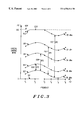
FIG. 3 is a graphical representation of the digital control word (on digital control axis 70) versus frequency (on frequency axis 72) for a plurality of power levels. When the radiotelephone 12 is required to transmit maximum available power, the digital control word is 0 for all frequencies. Thus, the maximum power word curve 90 has a value of zero for all frequencies.
When the radiotelephone 12 is set to transmit 28 dBm, one of the XF values stored in the memory 40 is used as the digital control word; these values fall on the 28 dBm word curve 92. When the radiotelephone 12 is set to transmit 26 dBm, the whole 28 dBm word curve 92 is offset by the XP2 offset control value 106 to form the 26 dBm word curve 94. Thus, the processing circuit 38 (FIG. 2) calculates the digital control word using an equation, so that a value falling on the 26 dBm word curve 94 is produced as the digital control word.
When the radiotelephone 12 is set to transmit 24 dBm, the whole 28 dBm word curve 92 is offset by the XP3 offset control value 108 to form the 24 dBm word curve 96. Thus, the processing circuit 38 (FIG. 2) calculates the digital control word using an equation so that a value falling on the 24 dBm word curve 96 is produced as the digital control word.
When the radiotelephone 12 is set to transmit 22 dBm, the whole 28 dBm word curve 92 is offset by the XP4 offset control value 110 to form the 22 dBm word curve 98. Thus, the processing circuit 38 (FIG. 2) calculates the digital control word using an equation so that a value falling on the 22 dBm word curve 98 is produced as the digital control word.
When the radiotelephone 12 is set to transmit 20 dBm, the whole 28 dBm word curve 92 is offset by the XP5 offset control value 112 to form the 20 dBm word curve 102. Thus, the processing circuit 38 (FIG. 2) calculates the digital control word using an equation so that a value falling on the 20 dBm word curve 102 is produced as the digital control word. Note, however, that at the 20 dBm power setting, the dynamic range of the variable impedance network 36 is beginning to be reached. This can be seen by the calculated control word 120 corresponding to frequency f2 on the 20 dBm word curve 102. The last load control DAC 42 state is 255, which corresponds to substantially the last impedance value that can be tuned to using the variable impedance network 36 (FIG. 2). In addition, for power level settings below 20 dBm, the minimum power word curve 104 is used for all frequencies.
TABLE 3
Digital
POUT Test XF Test XF XP XP Control
(dBm) Frequency Number Value Number Value Word
Max. Any 0
28 f1 XF1 50 XP1 0 50
28 f2 XF2 65 XP1 0 65
28 f3 XF3 52 XP1 0 52
28 f4 XF4 45 XP1 0 45
28 f5 XF5 43 XP1 0 43
28 f6 XF6 50 XP1 0 50
26 f1 XP2 30 80
26 f2 XP2 30 95
26 f3 XP2 30 82
26 f4 XP2 30 75
26 f5 XP2 30 73
26 f6 XP2 30 80
24 f1 XP3 90 140
24 f2 XP3 90 155
24 f3 XP3 90 142
24 f4 XP3 90 135
24 f5 XP3 90 133
24 f6 XP3 90 140
22 f1 XP4 140 190
22 f2 XP4 140 205
22 f3 XP4 140 192
22 f4 XP4 140 185
22 f5 XP4 140 183
22 f6 XP4 140 190
20 f1 XP5 200 250
20 f2 XP5 200 265
20 f3 XP5 200 252
20 f4 XP5 200 245
20 f5 XP5 200 243
20 f6 XP5 200 250
<20  Any 255
The processing circuit 38 can use other parameters to calculate the digital control or example, variations in the supply voltage can be compensated for by the variable impedance network 36. For example, a voltage monitoring circuit (not shown) coupled to the processing circuit 38 (FIG. 2) can detect a voltage of the battery (not shown) used to power the radiotelephone 12 (FIG. 1) as is known in the art.
The voltage monitoring circuit generates an indication of the voltage referred to as a voltage level signal. The voltage level signal is applied to voltage port 59 (FIG. 2) and the processing circuit 38 generates the digital control word responsive to the voltage level signal.
Table 1 shows that the processing circuit 38 actually uses two equations for power level settings between 28 and 20 dBm. Equation (1) is used when the supply voltage on supply port 52 is above 3.6 volts, and equation (2) is used when the supply voltage is below 3.6 volts. The control value XB0 is a predetermined constant representing an additional offset value for the digital word curves. FIG. 4 is a graphical representation of the 24 dBm digital word curve 96 versus frequency for three different supply values. This example is for an XB0 control value constant of 5. When the supply voltage is 3.6 volts, the nominal 24 dBm digital word curve 96 is plotted. When the supply voltage at supply port 52 (FIG. 2) is 3.8 V, equation (1) from Table 1 yields an additional offset of 5 (since XB0 is 5). Thus, the whole 24 dBm digital word curve 96 is moved up to form the 3.8 V-28 dBm digital word curve 150. Similarly, when the supply voltage at supply port 52 (FIG. 2) is 3.4 V, equation (2) from Table 1 yields an additional offset of 5 (since XB0 is 5). Thus, the whole 24 dBm digital word curve 96 is moved down to form the 3.4 V-28 dBm digital word curve 152.
Thus, when the supply voltage moves up (e.g. greater than 3.6 volts), the power amplifier 32 operating point moves away from saturation and thus becomes less efficient. By increasing the load impedance presented to the power amplifier 32 (e.g. by raising the digital word curve), the power amplifier 32 moves back closer to saturation. Conversely, if the supply voltage decreases, the power amplifier 32 becomes too saturated. By decreasing the power amplifier 32 load impedance (e.g. by lowering the digital word curve), the power amplifier 32 moves back away from being too saturated.
Accordingly, the minimum digital control word of 0 corresponds to an analog voltage at the output of the load control DAC 42 that is close to 0 volts. The maximum digital control word of 255 corresponds to an analog voltage at the output of the load control DAC 42 that is close to 3 volts.
The level shift circuit changes the analog voltage range. The minimum analog voltage of 0 volts from the load control DAC 42 is converted by the level shift circuit 44 (FIG. 2) to −1.5 V. The maximum analog voltage of 3 volts from the load control DAC 42 is converted by the level shift circuit 44 to +1.5 volts.
The variable impedance network 36 is configured so that a load control signal of −1.5 volts corresponds to the variable impedance network 36 presenting the maximum available load impedance to the power amplifier 32 (e.g. DAC state of 255 corresponds to maximum load impedance). A load control signal of +1.5 volts corresponds to the variable impedance network 36 presenting the minimum available load impedance to the power amplifier 32 (e.g. DAC state of 0 corresponds to minimum load impedance).
It is the processing circuit 38 that retrieves the control values from the memory 40 and uses the equations to generate the digital control word, which ultimately results in the load control signal after conversion to an analog signal and after level shifting by the level shift circuit 44. For battery voltages that yield an non-integer additional battery offset, the offset is rounded to the nearest integer value. Additional parameters, such as temperature, could be built into the equations used by the processing circuit 38.
In the illustrated embodiment, six frequencies within the frequency band are defined—f1 through f6. These frequencies designate frequency divisions. For operating frequencies other than the six designated frequencies, a control word corresponding to one of the six designated frequencies is used. For example, frequency 1 is designated as 824 MHz, and frequency 2 is designated as 829 MHz. For all operating frequencies between 824 and 826.5 MHz, the digital control word corresponding to f1 is used. For all operating frequencies between 826.5 MHz and 831.5 MHz, the digital control word corresponding to f2 is used. Thus, frequency spans of plus/minus 2.5 MHz are formed about the designated frequencies to define which control word to use. Frequency 1 only has a plus 2.5 MHz span, and frequency 6 only has a minus 2.5 MHz span.
FIG. 5 shows a Smith Chart with different load impedances to show how the load impedance of the variable impedance network 36 varies as a function of the digital control word. For a digital control word of 0 (corresponding to a load control signal of +1.5 V), minimum load impedance 160 results. Conversely, for a digital control word of 255 (corresponding to a load control signal of −1.5 V), maximum load impedance state 162 results.
FIG. 6 is a flowchart of a method of determining the various control values stored in the memory 40 (FIG. 2). The method starts at block 170, and at block 172, the test XF values are determined. These are the intermediate XF control values that are found initially so that the XP values can be determined. This step of determining the test XF values occurs at a first output power level (here 28 dBm). The method continues at block 174 where the XP control values are determined. These are the offset values for power levels lower than 28 dBm. Once the XP values are determined, they are stored in the memory 40 (FIG. 2) at block 176. At decision block 178, it is determined as to whether all of the power levels have been tested to generate the necessary XP values. If not, the method continues back at block 174.
If all XP power levels have been tested, it is determined at decision block 180 as to whether other parameters, such as a supply voltage offset constant is desired. If a battery voltage offset constant is desired, then the XB0 battery offset constant is determined at block 182. This XB0 constant is stored in the memory 40 (FIG. 2) at block 184. If no other parameters are desired, the method progresses from decision block 180 to block 186.
At block 186, the factory phasing procedure is performed to determine the new XF control values unique to each radiotelephone. This phasing is independently performed for each radiotelephone. The new, unique XF values for each radiotelephone is stored in the respective memory of each radiotelephone at block 188. The method ends at block 190.
A method of controlling the variable impedance network 36 at the output 33 of the power amplifier 32 operable in the radiotelephone 12 over a plurality of frequencies within a predetermined band of frequencies is shown in FIG. 7. The method begins at block 202, and at block 204 the processing unit 38 (FIG. 2) receives an indication of channel of operation and an indication of desired output power. If at decision block 206 it is desired to read other parameters such as batter voltage offset, then at block 208 the other parameter is received.
The method continues at block 210 where the processing unit retrieves stored control values (also referred to as control values) from the memory 40 (FIG. 2). Also at block 210, the processing unit either generates the digital control word directly from a stored control value, or the processing unit calculates the digital control word using the stored control values. In an alternate embodiment, all necessary digital control values are stored so that they can be retrieved directly from memory without the need for any calculation.
At block 212 the load control DAC 42 (FIG. 2) and the level shift circuit 44 (FIG. 2) produce the load control signal using the control values and in response to the indication of channel of operation and the indication of the desired output power. At block 213, the load control signal is applied to the variable impedance network 36 (FIG. 2), and at block 214 the variable impedance network 36 sets an impedance to present to the output 33 of the power amplifier 32 (FIG. 2) in response to the load control signal. The transmitter 16 (FIG. 1) is activated to transmit at block 215.
At block 215 the processing unit 38 (FIG. 2) constantly monitors the control signals to determine if there is a power level change at decision block 218 or a channel change at decision block 220. If there is no change, it is determined at decision block 222 whether any other parameters, such as supply voltage, that are being monitored have changed. If there are no changes and the transmitter 16 (FIG. 1) is not done transmitting at decision block 223, the method continues at block 216. If at decision block 223 the transmitter 16 (FIG. 1) is done transmitting, the transmitter 16 is de-activated and the method ends at block 240.
If the transmit power, channel, or other parameter changes, the processing circuit 38 (FIG. 2) reads the new setting at block 224. The new digital control word is calculated at block 226. The new load control signal is generated at block 228 and applied to the variable impedance network 36 (FIG. 2) at block 230. The variable impedance network 36 sets a new load impedance at block 232.
If at decision block 223 the transmitter 16 (FIG. 1) is not done transmitting, the method continues at block 216. If the transmitter 16 is done transmitting, the method ends at block 240.
FIG. 8 shows a first embodiment variable impedance network 400 that can be used to present various impedances to the power amplifier 32 (FIG. 2). The variable impedance network 400 includes first transmission line 250, fixed shunt capacitor 252 coupled to ground potential 254, second transmission line 256, and at least one variable element 258 coupled to ground potential 254. The variable element 258 can be selected from the group consisting of a varactor diode and a voltage variable capacitor (VVC).
The VVC is disclosed in U.S. Pat. No. 5,137,835, filed Oct. 15, 1991 by Kenneth D. Cornett, E. S. Ramakrishnan, Gary H. Shapiro, Raymond M. Caldwell, and Wei-Yean Howrig, the entire patent of which is incorporated herein by reference. However, any capacitor using a ferroelectric material which provides variable capacitance can be used. The VVC can comprise a pair of VVCs which are of opposite polarity to eliminate non-linearities during operation. The load control signal is applied to input 260 as a voltage to vary the capacitance of the variable element 258.
Other configurations of the variable impedance network 400 can be envisioned. For example, additional elements can be included, such as lumped element or distributed element inductors, additional transmission lines and capacitors, and additional variable elements.
FIG. 9 shows a second embodiment variable impedance network 500. The variable impedance network 500 includes first transmission line 270, a fixed shunt capacitor 272 coupled to ground potential 274, second transmission line 276, and a plurality of capacitors 278 coupled to ground that can be coupled and uncoupled the transmission line 276. The load control signal is applied to input 280 to open and close a plurality of switches 282 coupling the plurality of capacitors 278. The plurality of switches 282 can comprise, for example, PIN diodes or micro-electromechanical switches (MEMs). The plurality of capacitors 278 can be individually controlled.
Other configurations of the variable impedance network 602 can be envisioned without the use of the inventive faculty. For example, additional elements can be included, such as lumped element or distributed element inductors, additional transmission lines and capacitors, and additional variable elements. A combination of the variable impedance network 400 and the variable impedance network 500 could be used to increase the range of obtainable impedances. In addition, the load control signal can comprise multiple signals to separately control different variable impedance elements.
The factory phasing to generate the new XF control values for each radiotelephone helps tailor the variable impedance network 36 to each and every radiotelephone 12 that is shipped. Thus, the plurality of control values stored in the memory 40 (FIG. 2) correspond, at least in part, to amplifier load impedances that cause the power amplifier 32 (FIG. 2) to operate at substantially a predetermined output power over a plurality of frequencies within the predetermined band of frequencies when a predetermined input power is applied to the power amplifier.
The generation of the XF control values at the 28 dBm power level helps remove power amplifier 32 (FIG. 2) headroom that would otherwise be built in to compensate for worst case conditions. For example, the insertion loss of the static match circuit 34 (FIG. 2) varies across the band of frequencies. If the factory phasing were not performed, the power amplifier 32 would be biased to compensate for the worst insertion loss across the frequency band. At frequencies where the insertion loss is less than the worst case insertion loss, the power amplifier would no longer be at the most efficient operating point.
The additional XP offset values at a minimum can be used to increase the power amplifier efficiency for power levels lower than the power level corresponding to the XF power level. For example, for a constant envelope modulation scheme, the XF values can be offsets from the 28 dBm digital control word 92 (FIG. 3) to help increase maximum efficiency. Thus, the plurality of control values stored in the memory 40 (FIG. 2) can correspond, at least in part, to amplifier load impedances that cause the power amplifier 32 (FIG. 2) to have an efficiency greater than a predetermined amplifier efficiency over a plurality of frequencies within the predetermined band of frequencies.
In addition, for the case of a linear power amplifier used for linear modulation schemes, the control values can correspond to an output power as well as an adjacent channel power (ACP) that is less than a predetermined level of ACP. Thus, the plurality of control values stored in the memory can correspond, at least in part, to amplifier load impedances that cause the power amplifier 32 (FIG. 2) to operate at substantially a to predetermined output power and produce an adjacent channel power substantially less than a predetermined adjacent channel power when the power amplifier 32 (FIG. 2) operates over each of a plurality of frequencies within the predetermined band of frequencies. This results in operating the power amplifier 32 at a more efficient point.
Alternatively stated, a first set of the plurality of control values (referred to as the XF offset control values) stored in the memory 40 (FIG. 2) correspond to amplifier load impedances that cause the power amplifier 32 (FIG. 2) to operate at substantially a first output power and produce an adjacent channel power substantially less than a predetermined adjacent channel power when the power amplifier 32 operates over each of a plurality of frequencies within the predetermined band of frequencies.
Furthermore, a second set of the plurality of control values (referred to as the XP control values) stored in the memory 40 (FIG. 2) comprise offset control values used by the processing circuit to calculate the load control signal when the power amplifier 32 operates at a second output power. The processing circuit 38 (FIG. 2) calculates the load control signal to cause the variable impedance network 36 to present load impedances to the output 33 of the power amplifier 32, thereby causing the power amplifier 32 to have an efficiency greater than a predetermined amplifier efficiency over each of the plurality of frequencies within the predetermined band of frequencies.
The previous description of the preferred embodiments are provided to enable any person skilled in the art to use or make the power amplifier load adjust system. Various modifications to these embodiments will be readily apparent to those skilled in the art, and the generic principles defined herein may be applied to other embodiments without the use of the inventive faculty. For example, the load adjust system 200 (FIG. 2) can optionally include an isolator coupled to the output 48 of the variable impedance network 36. The isolator presents a substantially constant impedance to the output of the variable impedance network 36. This will provide extra predictability to the various impedances that the variable impedance network 36 provides to the power amplifier output 33.
The memory-based power amplifier load adjust system provides for a highly effective way of removing the operating point headroom that is typically designed into the power amplifier to handle worst case conditions and part to part variations. This provides for more efficient operation. In addition, storing and retrieving control values to calculate the load control signal in an open loop fashion provides an accurate and cost effective alternative to deriving the load control signal from power detection measurements in a closed loop system. This open loop load control based upon control values stored in memory allows for the operation of a power amplifier for both optimum efficiency and ACP performance over power and frequency. With the increased complexity of future generation radiotelephones, the power amplifier load adjust system used in a radiotelephone will provide a significant performance advantage over conventional radiotelephones.

Claims (15)

We claim:
1. A power amplifier load adjust system for use in a radiotelephone, the radiotelephone operable over a predetermined band of frequencies and powered by a battery, the power amplifier load adjust system comprising:
a power amplifier having an input and an output;
a variable impedance network coupled to the output of the power amplifier, the variable impedance network presenting a plurality of impedances to the output of the power amplifier responsive to a load control signal;
a control circuit for generating a transmit power command and a channel frequency command;
a memory for storing a plurality of control values as a function of power amplifier output power and frequency of operation; and
a processing circuit coupled to the variable impedance network, the control circuit, and the memory, the processing circuit for retrieving the plurality of control values stored in the memory and using the plurality of control values to generate the load control signal in response to the transmit power command and the channel frequency command.
2. The power amplifier load adjust system as in claim 1 further comprising a voltage monitoring circuit coupled to the processing circuit, the voltage monitoring circuit for detecting a voltage of the battery and generating an indication of the voltage, wherein the processing circuit produces the load control signal in response to the indication of the voltage, the transmit power command, and the channel frequency command.
3. The power amplifier load adjust system as in claim 1 wherein the plurality of control values stored in the memory correspond to amplifier load impedances that cause the power amplifier to have an efficiency greater than a predetermined amplifier efficiency over a plurality of frequencies within the predetermined band of frequencies.
4. The power amplifier load adjust system as in claim 1 wherein the plurality of control values stored in the memory correspond to amplifier load impedances that cause the power amplifier to operate at substantially a predetermined output power over a plurality of frequencies within the predetermined band of frequencies when a predetermined input power is applied to the power amplifier.
5. The power amplifier load adjust system as in claim 1 wherein the plurality of control values stored in the memory correspond to amplifier load impedances that cause the power amplifier to operate at substantially a predetermined output power and produce an adjacent channel power substantially less than a predetermined adjacent channel power when the power amplifier operates over each of a plurality of frequencies within the predetermined band of frequencies.
6. The power amplifier load adjust system as in claim 1 wherein the processing circuit uses the plurality of control values stored in the memory to calculate the load control signal using an equation.
7. The power amplifier load adjust system as in claim 1 wherein the processing circuit uses the plurality of control values stored in the memory to calculate the load control signal using an equation, the load control signal causing the variable impedance network to present load impedances to the output of the power amplifier that cause the power amplifier to have an efficiency greater than a predetermined amplifier efficiency over each of a plurality of frequencies within the predetermined band of frequencies.
8. The power amplifier load adjust system as in claim 1 wherein the processing circuit uses the plurality of control values stored in the memory to calculate the load control signal using an equation, the load control signal causing the variable impedance network to present load impedances to the output of the power amplifier that cause the power amplifier to operate at substantially a predetermined out put power over each of a plurality of frequencies within the predetermined band of frequencies when a predetermined input power is applied to the power amplifier.
9. The power amplifier load adjust system as in claim 1 wherein the processing circuit uses the plurality of control values stored in the memory to calculate the load control signal using an equation, the load control signal causing the variable impedance network to present load impedances to the output of the power amplifier that cause the power amplifier to operate at substantially a predetermined output power and to produce an adjacent channel power substantially less than a predetermined adjacent channel power when the power amplifier operates over each of a plurality of frequencies within the predetermined band of frequencies.
10. A power amplifier load adjust system for use in a radiotelephone, the radiotelephone operable over a predetermined band of frequencies, the power amplifier load adjust system comprising:
a power amplifier having an input and an output;
a variable impedance network coupled to the output of the power amplifier, the variable impedance network for presenting a plurality of impedances to the output of the power amplifier responsive to a load control signal;
a control circuit for generating a transmit power command and a channel frequency command;
a memory for storing a plurality of control values as a function of power amplifier output power and frequency of operation within the predetermined band of frequencies;
a processing circuit coupled to the variable impedance network, the control circuit, and the memory, the processing circuit for retrieving the plurality of control values stored in the memory and using the plurality of control values to generate a digital load control signal in response to the transmit power command and in response to the channel frequency command; and
a digital-to-analog converter (DAC) coupled to the processing circuit and the variable is impedance network, the DAC for converting the digital load control signal to the load control signal.
11. A power amplifier load adjust system for use in a radiotelephone, the radiotelephone operable over a predetermined band of frequencies, the power amplifier load adjust system comprising:
a power amplifier having an input and an output;
a variable impedance network coupled to the output of the power amplifier, the variable impedance network for presenting a plurality of impedances to the output of the power amplifier responsive to a load control signal;
a control circuit for generating a transmit power command and a channel frequency command;
a memory for storing a plurality of control values as a function of power amplifier output power and frequency of operation within the predetermined band of frequencies; and
a processing circuit coupled to the variable impedance network, the control circuit, and the memory, the processing circuit for retrieving the plurality of control values stored in the memory and using the plurality of control values to generate the load control signal in response to the transmit power command and in response to the channel frequency command,
wherein a first set of the plurality of control values stored in the memory correspond to amplifier load impedances that cause the power amplifier to operate at substantially a first output power and produce an adjacent channel power substantially less than a predetermined adjacent channel power when the power amplifier operates over each of a plurality of frequencies within the predetermined band of frequencies.
12. The power amplifier load adjust system as in claim 11 wherein a second set of the plurality of control values stored in memory comprise offset values used by the processing circuit to calculate the load control signal when the power amplifier operates at a second output power, wherein the processing circuit calculates the load control signal to cause the variable impedance network to present load impedances to the output of the power amplifier, thereby causing the power amplifier to have an efficiency greater than a predetermined amplifier efficiency over each of the plurality of frequencies within the predetermined band of frequencies.
13. A method of controlling a variable impedance network at an output of a power amplifier operable in a radiotelephone, the method comprising:
determining a plurality of control values that cause the variable impedance network to present impedances to the output of the power amplifier to cause the power amplifier to produce less than a predetermined amount of adjacent channel power when the power amplifier operates at each of a plurality of frequencies and at least one predetermined output power;
storing the plurality of control values;
generating a transmit power command;
generating a channel frequency command;
generating a load control signal using the plurality of control values and in response to the transmit power command and the channel frequency command;
applying the load control signal to the variable impedance network; and
presenting a load impedance to the output of the power amplifier responsive to the load control signal.
14. The method as in claim 13 further comprising:
calculating a control word using the plurality of control values, the transmit power command, and the channel frequency command; and
applying the control word to a digital-to-analog converter (DAC),
wherein the DAC uses the control word to generate the load control signal.
15. The method as in claim 3 further comprising generating a voltage level signal indicative of a battery voltage, wherein generating the load control signal is responsive to the voltage level signal.
US09/358,674 1999-07-22 1999-07-22 Memory-based amplifier load adjust system Expired - Lifetime US6556814B1 (en)

Priority Applications (8)

Application Number Priority Date Filing Date Title
US09/358,674 US6556814B1 (en) 1999-07-22 1999-07-22 Memory-based amplifier load adjust system
GB0017423A GB2356094B (en) 1999-07-22 2000-07-14 Memory-based amplifier load adjust system
DE10035066A DE10035066B4 (en) 1999-07-22 2000-07-17 System for the memory-based load adjustment of an amplifier
JP2000216760A JP2001068942A (en) 1999-07-22 2000-07-18 Amplification load adjustment system utilizing memory
BRPI0002979-3A BR0002979B1 (en) 1999-07-22 2000-07-19 power amplifier charge adjustment system.
CNB001213504A CN1172432C (en) 1999-07-22 2000-07-21 Amplifier load regulating system based on memory
KR10-2000-0042219A KR100502122B1 (en) 1999-07-22 2000-07-22 Memory-based amplifier load adjust system
US10/425,477 US20030199256A1 (en) 1999-07-22 2003-04-29 Memory-based amplifier load adjust system

Applications Claiming Priority (1)

Application Number Priority Date Filing Date Title
US09/358,674 US6556814B1 (en) 1999-07-22 1999-07-22 Memory-based amplifier load adjust system

Related Child Applications (1)

Application Number Title Priority Date Filing Date
US10/425,477 Continuation US20030199256A1 (en) 1999-07-22 2003-04-29 Memory-based amplifier load adjust system

Publications (1)

Publication Number Publication Date
US6556814B1 true US6556814B1 (en) 2003-04-29

Family

ID=23410590

Family Applications (2)

Application Number Title Priority Date Filing Date
US09/358,674 Expired - Lifetime US6556814B1 (en) 1999-07-22 1999-07-22 Memory-based amplifier load adjust system
US10/425,477 Abandoned US20030199256A1 (en) 1999-07-22 2003-04-29 Memory-based amplifier load adjust system

Family Applications After (1)

Application Number Title Priority Date Filing Date
US10/425,477 Abandoned US20030199256A1 (en) 1999-07-22 2003-04-29 Memory-based amplifier load adjust system

Country Status (7)

Country Link
US (2) US6556814B1 (en)
JP (1) JP2001068942A (en)
KR (1) KR100502122B1 (en)
CN (1) CN1172432C (en)
BR (1) BR0002979B1 (en)
DE (1) DE10035066B4 (en)
GB (1) GB2356094B (en)

Cited By (50)

* Cited by examiner, † Cited by third party
Publication number Priority date Publication date Assignee Title
US20030069042A1 (en) * 2001-06-27 2003-04-10 Tadahiro Sato Radio base station transceiver sub-system
US20030141927A1 (en) * 2002-01-31 2003-07-31 Kenneth Barnett Variable impedance load for a variable gain radio frequency amplifier
US6794935B2 (en) 2002-10-17 2004-09-21 Motorola Inc. Power amplification circuit and method for supplying power at a plurality of desired power output levels
US20050064827A1 (en) * 2003-09-22 2005-03-24 Schumacher Lawrence R. Amplifier power control in frequency hopping applications and methods
US20050124303A1 (en) * 2003-12-08 2005-06-09 M/A-Com, Inc. Compensating for load pull in electromagentic signal propagation using adaptive impedance matching
US20050233764A1 (en) * 2004-04-16 2005-10-20 M/A-Com Eurotec, B.V. Apparatus, methods and articles of manufacture for output impedance matching using multi-band signal processing
US6958665B2 (en) * 2003-04-02 2005-10-25 Raytheon Company Micro electro-mechanical system (MEMS) phase shifter
US6996080B1 (en) * 1999-07-23 2006-02-07 Itt Manufacturing Enterprises, Inc. Chip-synchronous CDMA multiplexer and method resulting in constant envelope signals
US7107030B1 (en) * 1999-06-24 2006-09-12 Nokia Mobile Phones Limited Transmitter and a modulator therefor
US20060223462A1 (en) * 2005-04-04 2006-10-05 Mahibur Rahman Dynamic gain and phase compensation for power amplifier load switching
US20060280261A1 (en) * 2005-06-10 2006-12-14 M/A-Com Eurotec Bv. System and method for controlling power output from a power amplifier
US20070200766A1 (en) * 2006-01-14 2007-08-30 Mckinzie William E Iii Adaptively tunable antennas and method of operation therefore
US20080122553A1 (en) * 2006-11-08 2008-05-29 Mckinzie William E Adaptive impedance matching module
US20090267588A1 (en) * 2008-04-23 2009-10-29 Schmitz Michael J Method and apparatus to dynamically control impedance to maximize power supply
US20100156552A1 (en) * 2006-01-14 2010-06-24 Paratek Microwave, Inc. Adaptive matching network
US20100164641A1 (en) * 2006-11-08 2010-07-01 Paratek Microwave, Inc. Method and apparatus for adaptive impedance matching
US20110014886A1 (en) * 2007-04-23 2011-01-20 Paratek Microwave, Inc. Techniques for improved adaptive impedance matching
US20110043298A1 (en) * 2006-11-08 2011-02-24 Paratek Microwave, Inc. System for establishing communication with a mobile device server
US20110053524A1 (en) * 2009-08-25 2011-03-03 Paratek Microwave, Inc. Method and apparatus for calibrating a communication device
US20110063042A1 (en) * 2000-07-20 2011-03-17 Paratek Microwave, Inc. Tunable microwave devices with auto-adjusting matching circuit
US20110086630A1 (en) * 2009-10-10 2011-04-14 Paratek Microwave, Inc. Method and apparatus for managing operations of a communication device
GB2476035A (en) * 2009-12-08 2011-06-15 Antenova Ltd Adaptive adjustment of RF amplifier load impedance to maximize efficiency
US20110227666A1 (en) * 2010-03-22 2011-09-22 Paratek Microwave, Inc. Method and apparatus for adapting a variable impedance network
CN102427338A (en) * 2011-09-26 2012-04-25 无锡易芯微电子有限公司 Signal amplifier capable of automatically changing input impedance and implementation method thereof
US8213886B2 (en) 2007-05-07 2012-07-03 Paratek Microwave, Inc. Hybrid techniques for antenna retuning utilizing transmit and receive power information
US8269683B2 (en) 2006-01-14 2012-09-18 Research In Motion Rf, Inc. Adaptively tunable antennas and method of operation therefore
US8421548B2 (en) 2008-09-24 2013-04-16 Research In Motion Rf, Inc. Methods for tuning an adaptive impedance matching network with a look-up table
US8428523B2 (en) 2007-11-14 2013-04-23 Research In Motion Rf, Inc. Tuning matching circuits for transmitter and receiver bands as a function of transmitter metrics
US8432234B2 (en) 2010-11-08 2013-04-30 Research In Motion Rf, Inc. Method and apparatus for tuning antennas in a communication device
US20130106507A1 (en) * 2011-10-27 2013-05-02 Marvell World Trade Ltd. Systems and methods for performing multi-modal power amplification
US20130122836A1 (en) * 2011-09-09 2013-05-16 Ethertronics, Inc. Pre-optimization of transmit circuits
US8594584B2 (en) 2011-05-16 2013-11-26 Blackberry Limited Method and apparatus for tuning a communication device
US8626083B2 (en) 2011-05-16 2014-01-07 Blackberry Limited Method and apparatus for tuning a communication device
US8655286B2 (en) 2011-02-25 2014-02-18 Blackberry Limited Method and apparatus for tuning a communication device
US8712340B2 (en) 2011-02-18 2014-04-29 Blackberry Limited Method and apparatus for radio antenna frequency tuning
USRE44998E1 (en) 2000-07-20 2014-07-08 Blackberry Limited Optimized thin film capacitors
US8860526B2 (en) 2010-04-20 2014-10-14 Blackberry Limited Method and apparatus for managing interference in a communication device
US8948889B2 (en) 2012-06-01 2015-02-03 Blackberry Limited Methods and apparatus for tuning circuit components of a communication device
US20150119094A1 (en) * 2013-10-25 2015-04-30 Motorola Solutions, Inc. Method and apparatus for adjusting transmission power in a two-way device based on battery impedance
US9246223B2 (en) 2012-07-17 2016-01-26 Blackberry Limited Antenna tuning for multiband operation
US9350405B2 (en) 2012-07-19 2016-05-24 Blackberry Limited Method and apparatus for antenna tuning and power consumption management in a communication device
US9362891B2 (en) 2012-07-26 2016-06-07 Blackberry Limited Methods and apparatus for tuning a communication device
US9374113B2 (en) 2012-12-21 2016-06-21 Blackberry Limited Method and apparatus for adjusting the timing of radio antenna tuning
US9413066B2 (en) 2012-07-19 2016-08-09 Blackberry Limited Method and apparatus for beam forming and antenna tuning in a communication device
US9769826B2 (en) 2011-08-05 2017-09-19 Blackberry Limited Method and apparatus for band tuning in a communication device
US9853363B2 (en) 2012-07-06 2017-12-26 Blackberry Limited Methods and apparatus to control mutual coupling between antennas
US10003393B2 (en) 2014-12-16 2018-06-19 Blackberry Limited Method and apparatus for antenna selection
US10163574B2 (en) 2005-11-14 2018-12-25 Blackberry Limited Thin films capacitors
US10404295B2 (en) 2012-12-21 2019-09-03 Blackberry Limited Method and apparatus for adjusting the timing of radio antenna tuning
US10644756B2 (en) * 2018-07-30 2020-05-05 Nxp B.V. Transmitter calibration for NFC (near field communication) device

Families Citing this family (18)

* Cited by examiner, † Cited by third party
Publication number Priority date Publication date Assignee Title
GB0121390D0 (en) * 2001-09-05 2001-10-24 Koninkl Philips Electronics Nv Power amplifier
SE0202989D0 (en) * 2002-10-10 2002-10-10 Allgon Mobile Comm Ab Power amplifier efficiency
US6798295B2 (en) * 2002-12-13 2004-09-28 Cree Microwave, Inc. Single package multi-chip RF power amplifier
EP1605589A4 (en) * 2003-03-14 2007-03-21 Ntt Docomo Inc Matching circuit
US7342955B2 (en) * 2003-04-23 2008-03-11 Motorola Inc Apparatus and method for mobile communication device transmission
JP4175545B2 (en) 2004-09-03 2008-11-05 ソニー・エリクソン・モバイルコミュニケーションズ株式会社 Wireless communication terminal
JP4606843B2 (en) * 2004-11-01 2011-01-05 京セラ株式会社 Wireless communication module, communication terminal, and impedance matching method
DE102005050148B4 (en) * 2005-10-19 2010-08-12 Infineon Technologies Ag Transmitting unit for a mobile device, use of a transmitting unit in a transmitting / receiving unit in a mobile device, and method for signal processing in a transmitting unit for a mobile device
EP2030317B1 (en) * 2006-06-09 2011-08-10 Telefonaktiebolaget LM Ericsson (publ) High efficiency linear power amplifiers with load compensation
DE102006032961A1 (en) * 2006-07-17 2008-02-21 Rohde & Schwarz Gmbh & Co. Kg Method and system for determining the dependence between device parameters of a mobile device and signal sizes
US8311591B2 (en) * 2009-05-13 2012-11-13 Alcatel Lucent Closed-loop efficiency modulation for use in network powered applications
JP2011234155A (en) * 2010-04-28 2011-11-17 Renesas Electronics Corp Transmitter
US8611834B2 (en) 2010-11-01 2013-12-17 Cree, Inc. Matching network for transmission circuitry
US20120154070A1 (en) * 2010-12-16 2012-06-21 Sony Ericsson Mobile Communications Ab Closed Loop Antenna Tuning Using Transmit Power Control Commands
CN102355223B (en) * 2011-08-10 2014-08-27 锐迪科创微电子(北京)有限公司 Single-chip GSM (Global System for Mobile Communications) radio-frequency antenna switch module and GSM radio-frequency front end
CN103532495B (en) * 2012-07-02 2016-12-21 华为终端有限公司 A kind of adjust the method for power amplifier voltage, Apparatus and system
CN105099582B (en) * 2015-07-20 2018-06-01 联想(北京)有限公司 A kind of load setting method and system
CN112148052B (en) * 2020-09-28 2022-10-11 刘承鑫 Portable adjustable stable alternating-current high-voltage generation system

Citations (7)

* Cited by examiner, † Cited by third party
Publication number Priority date Publication date Assignee Title
US4965607A (en) * 1987-04-30 1990-10-23 Br Communications, Inc. Antenna coupler
US5170496A (en) * 1989-06-22 1992-12-08 Texas Instruments Deutschland Gmbh Circuit arrangement for matching the resonant frequency of an antenna resonant circuit to the output frequency of a transmitter output stage
US5673001A (en) 1995-06-07 1997-09-30 Motorola, Inc. Method and apparatus for amplifying a signal
US5862458A (en) * 1995-04-18 1999-01-19 Nec Corporation Impedance matching circuit in transmitter circuit and control method thereof
KR19990023367A (en) 1997-08-06 1999-03-25 가네꼬 히사시 Transmission power control device which can vary transmission power widely
US6215987B1 (en) * 1997-06-06 2001-04-10 Nec Corporation Mobile communication transmitter capable of selectively activating amplifiers
US6246727B1 (en) * 1996-07-10 2001-06-12 Allgon Ab Method and system for tuning resonance modules

Family Cites Families (17)

* Cited by examiner, † Cited by third party
Publication number Priority date Publication date Assignee Title
JPS5851453B2 (en) * 1980-09-29 1983-11-16 日本電信電話株式会社 transmitting device
JPS63253730A (en) * 1987-04-09 1988-10-20 Nec Corp Power amplifier
JPS63272107A (en) * 1987-04-30 1988-11-09 Hitachi Ltd High frequency power amplifier
DE8916266U1 (en) * 1988-11-17 1996-06-05 Motorola Inc Power amplifier for radio frequency signals
US5276912A (en) * 1990-02-06 1994-01-04 Motorola, Inc. Radio frequency power amplifier having variable output power
JP2647730B2 (en) * 1990-06-01 1997-08-27 ソニー株式会社 Mobile phone equipment
JPH0480140U (en) * 1990-11-26 1992-07-13
JPH05343929A (en) * 1992-06-10 1993-12-24 Fujitsu Ltd Power amplifier
US5564086A (en) * 1993-11-29 1996-10-08 Motorola, Inc. Method and apparatus for enhancing an operating characteristic of a radio transmitter
DE69630512T2 (en) * 1995-09-29 2004-05-06 Matsushita Electric Industrial Co., Ltd., Kadoma POWER AMPLIFIER AND COMMUNICATION DEVICE
JPH09232887A (en) * 1996-02-28 1997-09-05 Matsushita Electron Corp High frequency power amplifier
US20010028252A1 (en) * 1996-10-18 2001-10-11 Pertti K. Ikalainen Impedance adapting circuit
US5880635A (en) * 1997-04-16 1999-03-09 Sony Corporation Apparatus for optimizing the performance of a power amplifier
DE19757142A1 (en) * 1997-12-20 1999-07-08 Philips Patentverwaltung Cellular device
FI990687A (en) * 1999-03-29 2000-09-30 Nokia Mobile Phones Ltd Method of adapting an antenna for a wireless communication device
US6160449A (en) * 1999-07-22 2000-12-12 Motorola, Inc. Power amplifying circuit with load adjust for control of adjacent and alternate channel power
US6252456B1 (en) * 1999-07-29 2001-06-26 Motorola, Inc. Power amplifier load controller and method for controlling a power amplifier load

Patent Citations (8)

* Cited by examiner, † Cited by third party
Publication number Priority date Publication date Assignee Title
US4965607A (en) * 1987-04-30 1990-10-23 Br Communications, Inc. Antenna coupler
US5170496A (en) * 1989-06-22 1992-12-08 Texas Instruments Deutschland Gmbh Circuit arrangement for matching the resonant frequency of an antenna resonant circuit to the output frequency of a transmitter output stage
US5862458A (en) * 1995-04-18 1999-01-19 Nec Corporation Impedance matching circuit in transmitter circuit and control method thereof
US5673001A (en) 1995-06-07 1997-09-30 Motorola, Inc. Method and apparatus for amplifying a signal
US6246727B1 (en) * 1996-07-10 2001-06-12 Allgon Ab Method and system for tuning resonance modules
US6215987B1 (en) * 1997-06-06 2001-04-10 Nec Corporation Mobile communication transmitter capable of selectively activating amplifiers
KR19990023367A (en) 1997-08-06 1999-03-25 가네꼬 히사시 Transmission power control device which can vary transmission power widely
US20010014587A1 (en) 1997-08-06 2001-08-16 Masaki Ichihara Transmission power control device capable of varying a transmission power at a wide range

Cited By (131)

* Cited by examiner, † Cited by third party
Publication number Priority date Publication date Assignee Title
US7107030B1 (en) * 1999-06-24 2006-09-12 Nokia Mobile Phones Limited Transmitter and a modulator therefor
US6996080B1 (en) * 1999-07-23 2006-02-07 Itt Manufacturing Enterprises, Inc. Chip-synchronous CDMA multiplexer and method resulting in constant envelope signals
US8896391B2 (en) 2000-07-20 2014-11-25 Blackberry Limited Tunable microwave devices with auto-adjusting matching circuit
US9431990B2 (en) 2000-07-20 2016-08-30 Blackberry Limited Tunable microwave devices with auto-adjusting matching circuit
US8744384B2 (en) 2000-07-20 2014-06-03 Blackberry Limited Tunable microwave devices with auto-adjusting matching circuit
USRE44998E1 (en) 2000-07-20 2014-07-08 Blackberry Limited Optimized thin film capacitors
US8693963B2 (en) 2000-07-20 2014-04-08 Blackberry Limited Tunable microwave devices with auto-adjusting matching circuit
US20110063042A1 (en) * 2000-07-20 2011-03-17 Paratek Microwave, Inc. Tunable microwave devices with auto-adjusting matching circuit
US9768752B2 (en) 2000-07-20 2017-09-19 Blackberry Limited Tunable microwave devices with auto-adjusting matching circuit
US9948270B2 (en) 2000-07-20 2018-04-17 Blackberry Limited Tunable microwave devices with auto-adjusting matching circuit
US6963746B2 (en) * 2001-06-27 2005-11-08 Fujitsu Limited Radio base station transceiver sub-system
US20030069042A1 (en) * 2001-06-27 2003-04-10 Tadahiro Sato Radio base station transceiver sub-system
US20030141927A1 (en) * 2002-01-31 2003-07-31 Kenneth Barnett Variable impedance load for a variable gain radio frequency amplifier
US7113033B2 (en) * 2002-01-31 2006-09-26 Qualcomm Incorporated Variable impedance load for a variable gain radio frequency amplifier
US6794935B2 (en) 2002-10-17 2004-09-21 Motorola Inc. Power amplification circuit and method for supplying power at a plurality of desired power output levels
US6958665B2 (en) * 2003-04-02 2005-10-25 Raytheon Company Micro electro-mechanical system (MEMS) phase shifter
KR101119871B1 (en) * 2003-09-22 2012-03-13 모토로라 모빌리티, 인크. Amplifier power control in frequency hopping applications and methods
US20050064827A1 (en) * 2003-09-22 2005-03-24 Schumacher Lawrence R. Amplifier power control in frequency hopping applications and methods
US6927627B2 (en) * 2003-09-22 2005-08-09 Motorola, Inc. Amplifier power control in frequency hopping applications and methods
WO2005034337A3 (en) * 2003-09-22 2005-06-30 Motorola Inc Amplifier power control in frequency hopping applications and methods
US7343138B2 (en) 2003-12-08 2008-03-11 M/A-Com, Inc. Compensating for load pull in electromagentic signal propagation using adaptive impedance matching
US20050124303A1 (en) * 2003-12-08 2005-06-09 M/A-Com, Inc. Compensating for load pull in electromagentic signal propagation using adaptive impedance matching
US20050233764A1 (en) * 2004-04-16 2005-10-20 M/A-Com Eurotec, B.V. Apparatus, methods and articles of manufacture for output impedance matching using multi-band signal processing
US7440729B2 (en) 2004-04-16 2008-10-21 M/A-Com Eurotec B.V. Apparatus, methods and articles of manufacture for output impedance matching using multi-band signal processing
US7346317B2 (en) 2005-04-04 2008-03-18 Freescale Semiconductor, Inc. Dynamic gain and phase compensation for power amplifier load switching
US20060223462A1 (en) * 2005-04-04 2006-10-05 Mahibur Rahman Dynamic gain and phase compensation for power amplifier load switching
US20060280261A1 (en) * 2005-06-10 2006-12-14 M/A-Com Eurotec Bv. System and method for controlling power output from a power amplifier
US10163574B2 (en) 2005-11-14 2018-12-25 Blackberry Limited Thin films capacitors
US8620246B2 (en) 2006-01-14 2013-12-31 Blackberry Limited Adaptive impedance matching module (AIMM) control architectures
US8405563B2 (en) 2006-01-14 2013-03-26 Research In Motion Rf, Inc. Adaptively tunable antennas incorporating an external probe to monitor radiated power
US20070200766A1 (en) * 2006-01-14 2007-08-30 Mckinzie William E Iii Adaptively tunable antennas and method of operation therefore
US20100156552A1 (en) * 2006-01-14 2010-06-24 Paratek Microwave, Inc. Adaptive matching network
US8942657B2 (en) 2006-01-14 2015-01-27 Blackberry Limited Adaptive matching network
US8620247B2 (en) 2006-01-14 2013-12-31 Blackberry Limited Adaptive impedance matching module (AIMM) control architectures
US10177731B2 (en) 2006-01-14 2019-01-08 Blackberry Limited Adaptive matching network
US8463218B2 (en) 2006-01-14 2013-06-11 Research In Motion Rf, Inc. Adaptive matching network
US8269683B2 (en) 2006-01-14 2012-09-18 Research In Motion Rf, Inc. Adaptively tunable antennas and method of operation therefore
US9853622B2 (en) 2006-01-14 2017-12-26 Blackberry Limited Adaptive matching network
US8325097B2 (en) 2006-01-14 2012-12-04 Research In Motion Rf, Inc. Adaptively tunable antennas and method of operation therefore
US8564381B2 (en) 2006-11-08 2013-10-22 Blackberry Limited Method and apparatus for adaptive impedance matching
US8680934B2 (en) 2006-11-08 2014-03-25 Blackberry Limited System for establishing communication with a mobile device server
US9130543B2 (en) 2006-11-08 2015-09-08 Blackberry Limited Method and apparatus for adaptive impedance matching
US10020828B2 (en) 2006-11-08 2018-07-10 Blackberry Limited Adaptive impedance matching apparatus, system and method with improved dynamic range
US20110043298A1 (en) * 2006-11-08 2011-02-24 Paratek Microwave, Inc. System for establishing communication with a mobile device server
US8299867B2 (en) 2006-11-08 2012-10-30 Research In Motion Rf, Inc. Adaptive impedance matching module
US9419581B2 (en) 2006-11-08 2016-08-16 Blackberry Limited Adaptive impedance matching apparatus, system and method with improved dynamic range
US8217731B2 (en) 2006-11-08 2012-07-10 Paratek Microwave, Inc. Method and apparatus for adaptive impedance matching
US20080122553A1 (en) * 2006-11-08 2008-05-29 Mckinzie William E Adaptive impedance matching module
US8558633B2 (en) 2006-11-08 2013-10-15 Blackberry Limited Method and apparatus for adaptive impedance matching
US8217732B2 (en) 2006-11-08 2012-07-10 Paratek Microwave, Inc. Method and apparatus for adaptive impedance matching
US9722577B2 (en) 2006-11-08 2017-08-01 Blackberry Limited Method and apparatus for adaptive impedance matching
US20100164641A1 (en) * 2006-11-08 2010-07-01 Paratek Microwave, Inc. Method and apparatus for adaptive impedance matching
US10050598B2 (en) 2006-11-08 2018-08-14 Blackberry Limited Method and apparatus for adaptive impedance matching
US20100164640A1 (en) * 2006-11-08 2010-07-01 Paratek Microwave, Inc. Method and apparatus for adaptive impedance matching
US9698748B2 (en) 2007-04-23 2017-07-04 Blackberry Limited Adaptive impedance matching
US8620236B2 (en) * 2007-04-23 2013-12-31 Blackberry Limited Techniques for improved adaptive impedance matching
US20110014886A1 (en) * 2007-04-23 2011-01-20 Paratek Microwave, Inc. Techniques for improved adaptive impedance matching
US8781417B2 (en) 2007-05-07 2014-07-15 Blackberry Limited Hybrid techniques for antenna retuning utilizing transmit and receive power information
US9119152B2 (en) 2007-05-07 2015-08-25 Blackberry Limited Hybrid techniques for antenna retuning utilizing transmit and receive power information
US8457569B2 (en) 2007-05-07 2013-06-04 Research In Motion Rf, Inc. Hybrid techniques for antenna retuning utilizing transmit and receive power information
US8213886B2 (en) 2007-05-07 2012-07-03 Paratek Microwave, Inc. Hybrid techniques for antenna retuning utilizing transmit and receive power information
US8798555B2 (en) 2007-11-14 2014-08-05 Blackberry Limited Tuning matching circuits for transmitter and receiver bands as a function of the transmitter metrics
USRE48435E1 (en) 2007-11-14 2021-02-09 Nxp Usa, Inc. Tuning matching circuits for transmitter and receiver bands as a function of the transmitter metrics
US8428523B2 (en) 2007-11-14 2013-04-23 Research In Motion Rf, Inc. Tuning matching circuits for transmitter and receiver bands as a function of transmitter metrics
USRE47412E1 (en) 2007-11-14 2019-05-28 Blackberry Limited Tuning matching circuits for transmitter and receiver bands as a function of the transmitter metrics
US20090267588A1 (en) * 2008-04-23 2009-10-29 Schmitz Michael J Method and apparatus to dynamically control impedance to maximize power supply
US9698758B2 (en) 2008-09-24 2017-07-04 Blackberry Limited Methods for tuning an adaptive impedance matching network with a look-up table
US8421548B2 (en) 2008-09-24 2013-04-16 Research In Motion Rf, Inc. Methods for tuning an adaptive impedance matching network with a look-up table
US8674783B2 (en) 2008-09-24 2014-03-18 Blackberry Limited Methods for tuning an adaptive impedance matching network with a look-up table
US8957742B2 (en) 2008-09-24 2015-02-17 Blackberry Limited Methods for tuning an adaptive impedance matching network with a look-up table
US8787845B2 (en) 2009-08-25 2014-07-22 Blackberry Limited Method and apparatus for calibrating a communication device
US8472888B2 (en) 2009-08-25 2013-06-25 Research In Motion Rf, Inc. Method and apparatus for calibrating a communication device
US9020446B2 (en) 2009-08-25 2015-04-28 Blackberry Limited Method and apparatus for calibrating a communication device
US20110053524A1 (en) * 2009-08-25 2011-03-03 Paratek Microwave, Inc. Method and apparatus for calibrating a communication device
US20110086630A1 (en) * 2009-10-10 2011-04-14 Paratek Microwave, Inc. Method and apparatus for managing operations of a communication device
US9853663B2 (en) 2009-10-10 2017-12-26 Blackberry Limited Method and apparatus for managing operations of a communication device
US9026062B2 (en) 2009-10-10 2015-05-05 Blackberry Limited Method and apparatus for managing operations of a communication device
US10659088B2 (en) 2009-10-10 2020-05-19 Nxp Usa, Inc. Method and apparatus for managing operations of a communication device
GB2476035B (en) * 2009-12-08 2016-06-01 Microsoft Technology Licensing Llc Improvements relating to power amplifiers and antennas
GB2476035A (en) * 2009-12-08 2011-06-15 Antenova Ltd Adaptive adjustment of RF amplifier load impedance to maximize efficiency
US10615769B2 (en) 2010-03-22 2020-04-07 Blackberry Limited Method and apparatus for adapting a variable impedance network
US9608591B2 (en) 2010-03-22 2017-03-28 Blackberry Limited Method and apparatus for adapting a variable impedance network
US10263595B2 (en) 2010-03-22 2019-04-16 Blackberry Limited Method and apparatus for adapting a variable impedance network
US9548716B2 (en) 2010-03-22 2017-01-17 Blackberry Limited Method and apparatus for adapting a variable impedance network
US8803631B2 (en) 2010-03-22 2014-08-12 Blackberry Limited Method and apparatus for adapting a variable impedance network
US9742375B2 (en) 2010-03-22 2017-08-22 Blackberry Limited Method and apparatus for adapting a variable impedance network
US20110227666A1 (en) * 2010-03-22 2011-09-22 Paratek Microwave, Inc. Method and apparatus for adapting a variable impedance network
US8860526B2 (en) 2010-04-20 2014-10-14 Blackberry Limited Method and apparatus for managing interference in a communication device
US9564944B2 (en) 2010-04-20 2017-02-07 Blackberry Limited Method and apparatus for managing interference in a communication device
US9941922B2 (en) 2010-04-20 2018-04-10 Blackberry Limited Method and apparatus for managing interference in a communication device
US9450637B2 (en) 2010-04-20 2016-09-20 Blackberry Limited Method and apparatus for managing interference in a communication device
US8860525B2 (en) 2010-04-20 2014-10-14 Blackberry Limited Method and apparatus for managing interference in a communication device
US8432234B2 (en) 2010-11-08 2013-04-30 Research In Motion Rf, Inc. Method and apparatus for tuning antennas in a communication device
US9379454B2 (en) 2010-11-08 2016-06-28 Blackberry Limited Method and apparatus for tuning antennas in a communication device
US9263806B2 (en) 2010-11-08 2016-02-16 Blackberry Limited Method and apparatus for tuning antennas in a communication device
US8712340B2 (en) 2011-02-18 2014-04-29 Blackberry Limited Method and apparatus for radio antenna frequency tuning
US9231643B2 (en) 2011-02-18 2016-01-05 Blackberry Limited Method and apparatus for radio antenna frequency tuning
US9935674B2 (en) 2011-02-18 2018-04-03 Blackberry Limited Method and apparatus for radio antenna frequency tuning
US9698858B2 (en) 2011-02-18 2017-07-04 Blackberry Limited Method and apparatus for radio antenna frequency tuning
US10979095B2 (en) 2011-02-18 2021-04-13 Nxp Usa, Inc. Method and apparatus for radio antenna frequency tuning
US8655286B2 (en) 2011-02-25 2014-02-18 Blackberry Limited Method and apparatus for tuning a communication device
US9473216B2 (en) 2011-02-25 2016-10-18 Blackberry Limited Method and apparatus for tuning a communication device
US9716311B2 (en) 2011-05-16 2017-07-25 Blackberry Limited Method and apparatus for tuning a communication device
US8626083B2 (en) 2011-05-16 2014-01-07 Blackberry Limited Method and apparatus for tuning a communication device
US8594584B2 (en) 2011-05-16 2013-11-26 Blackberry Limited Method and apparatus for tuning a communication device
US10218070B2 (en) 2011-05-16 2019-02-26 Blackberry Limited Method and apparatus for tuning a communication device
US9769826B2 (en) 2011-08-05 2017-09-19 Blackberry Limited Method and apparatus for band tuning in a communication device
US10624091B2 (en) 2011-08-05 2020-04-14 Blackberry Limited Method and apparatus for band tuning in a communication device
US20130122836A1 (en) * 2011-09-09 2013-05-16 Ethertronics, Inc. Pre-optimization of transmit circuits
US8843085B2 (en) * 2011-09-09 2014-09-23 Ethertronics, Inc. Pre-optimization of transmit circuits
CN102427338A (en) * 2011-09-26 2012-04-25 无锡易芯微电子有限公司 Signal amplifier capable of automatically changing input impedance and implementation method thereof
CN102427338B (en) * 2011-09-26 2015-05-20 无锡易芯微电子有限公司 Signal amplifier capable of automatically changing input impedance and implementation method thereof
US8957733B2 (en) * 2011-10-27 2015-02-17 Marvell World Trade Ltd. Systems and methods for performing multi-modal power amplification
US20130106507A1 (en) * 2011-10-27 2013-05-02 Marvell World Trade Ltd. Systems and methods for performing multi-modal power amplification
US9671765B2 (en) 2012-06-01 2017-06-06 Blackberry Limited Methods and apparatus for tuning circuit components of a communication device
US8948889B2 (en) 2012-06-01 2015-02-03 Blackberry Limited Methods and apparatus for tuning circuit components of a communication device
US9853363B2 (en) 2012-07-06 2017-12-26 Blackberry Limited Methods and apparatus to control mutual coupling between antennas
US9246223B2 (en) 2012-07-17 2016-01-26 Blackberry Limited Antenna tuning for multiband operation
US9350405B2 (en) 2012-07-19 2016-05-24 Blackberry Limited Method and apparatus for antenna tuning and power consumption management in a communication device
US9413066B2 (en) 2012-07-19 2016-08-09 Blackberry Limited Method and apparatus for beam forming and antenna tuning in a communication device
US9941910B2 (en) 2012-07-19 2018-04-10 Blackberry Limited Method and apparatus for antenna tuning and power consumption management in a communication device
US9362891B2 (en) 2012-07-26 2016-06-07 Blackberry Limited Methods and apparatus for tuning a communication device
US9768810B2 (en) 2012-12-21 2017-09-19 Blackberry Limited Method and apparatus for adjusting the timing of radio antenna tuning
US10404295B2 (en) 2012-12-21 2019-09-03 Blackberry Limited Method and apparatus for adjusting the timing of radio antenna tuning
US9374113B2 (en) 2012-12-21 2016-06-21 Blackberry Limited Method and apparatus for adjusting the timing of radio antenna tuning
US10700719B2 (en) 2012-12-21 2020-06-30 Nxp Usa, Inc. Method and apparatus for adjusting the timing of radio antenna tuning
US9131452B2 (en) * 2013-10-25 2015-09-08 Motorola Solutions, Inc. Method and apparatus for adjusting transmission power in a two-way device based on battery impedance
US20150119094A1 (en) * 2013-10-25 2015-04-30 Motorola Solutions, Inc. Method and apparatus for adjusting transmission power in a two-way device based on battery impedance
US10651918B2 (en) 2014-12-16 2020-05-12 Nxp Usa, Inc. Method and apparatus for antenna selection
US10003393B2 (en) 2014-12-16 2018-06-19 Blackberry Limited Method and apparatus for antenna selection
US10644756B2 (en) * 2018-07-30 2020-05-05 Nxp B.V. Transmitter calibration for NFC (near field communication) device

Also Published As

Publication number Publication date
CN1172432C (en) 2004-10-20
GB2356094B (en) 2002-02-13
BR0002979B1 (en) 2012-11-27
GB0017423D0 (en) 2000-08-30
KR20010015417A (en) 2001-02-26
GB2356094A (en) 2001-05-09
CN1282139A (en) 2001-01-31
KR100502122B1 (en) 2005-07-19
US20030199256A1 (en) 2003-10-23
DE10035066B4 (en) 2009-07-16
DE10035066A1 (en) 2001-03-15
JP2001068942A (en) 2001-03-16
BR0002979A (en) 2001-07-31

Similar Documents

Publication Publication Date Title
US6556814B1 (en) Memory-based amplifier load adjust system
US6438360B1 (en) Amplifier system with load control to produce an amplitude envelope
KR100372856B1 (en) Power amplifying circuit with load adjust for control of adjacent and alternate channel power
KR100359601B1 (en) Load envelope following amplifier system
US6166598A (en) Power amplifying circuit with supply adjust to control adjacent and alternate channel power
US5604924A (en) Radio communication apparatus in which output power is controlled by pulse width modulation using a mobile attenuation code
CA2176551C (en) Method and apparatus for amplifying a signal
US6973334B2 (en) Cellular telephone
US7062236B2 (en) Transmitter circuits
EP1107449B1 (en) Non-linear distortion compensation circuit, transmitter device to be employed in the same and mobile communication unit
KR100312367B1 (en) Mobile communication device and method
US6407634B1 (en) Linear envelope tracking RF power amplifier with adaptive analog signal processing
KR20020081069A (en) High-frequency amplifier circuit and radio communication apparatus using same
US5933767A (en) Apparatus and method for tuning the gain of a transmitter utilizing cartesian feedback
BR9913792B1 (en) amplifier and control circuit, process for controlling a power amplifier circuit, and transmitter for transmitting an output signal.
EP1104119B1 (en) Transmitter adjusting output power
GB2347288A (en) Large dynamic range transmitter power control for a CDMA mobile phone
JPH08316759A (en) Broad band amplifier
MXPA00007175A (en) Amplification load adjustment system utilizing memory
JPH05343929A (en) Power amplifier
MXPA00007176A (en) Power amplifying circuit with load adjust for control of adjacent and alternate channel power
JP2002232328A (en) Nonlinear phase distortion compensation device

Legal Events

Date Code Title Description
AS Assignment

Owner name: MOTOROLA, INC., ILLINOIS

Free format text: ASSIGNMENT OF ASSIGNORS INTEREST;ASSIGNORS:KLOMSDORF, ARMIN;WINKELMANN, LUKE EDWARD;LANDHERR, MICHAEL;REEL/FRAME:010123/0757

Effective date: 19990720

STCF Information on status: patent grant

Free format text: PATENTED CASE

CC Certificate of correction
FPAY Fee payment

Year of fee payment: 4

FPAY Fee payment

Year of fee payment: 8

AS Assignment

Owner name: MOTOROLA MOBILITY, INC, ILLINOIS

Free format text: ASSIGNMENT OF ASSIGNORS INTEREST;ASSIGNOR:MOTOROLA, INC;REEL/FRAME:025673/0558

Effective date: 20100731

AS Assignment

Owner name: MOTOROLA MOBILITY LLC, ILLINOIS

Free format text: CHANGE OF NAME;ASSIGNOR:MOTOROLA MOBILITY, INC.;REEL/FRAME:029216/0282

Effective date: 20120622

FPAY Fee payment

Year of fee payment: 12

AS Assignment

Owner name: GOOGLE TECHNOLOGY HOLDINGS LLC, CALIFORNIA

Free format text: ASSIGNMENT OF ASSIGNORS INTEREST;ASSIGNOR:MOTOROLA MOBILITY LLC;REEL/FRAME:034430/0001

Effective date: 20141028