US6583015B2 - Gate technology for strained surface channel and strained buried channel MOSFET devices - Google Patents
Gate technology for strained surface channel and strained buried channel MOSFET devices Download PDFInfo
- Publication number
- US6583015B2 US6583015B2 US09/923,207 US92320701A US6583015B2 US 6583015 B2 US6583015 B2 US 6583015B2 US 92320701 A US92320701 A US 92320701A US 6583015 B2 US6583015 B2 US 6583015B2
- Authority
- US
- United States
- Prior art keywords
- layer
- strained
- sige
- strained channel
- providing
- Prior art date
- Legal status (The legal status is an assumption and is not a legal conclusion. Google has not performed a legal analysis and makes no representation as to the accuracy of the status listed.)
- Expired - Lifetime
Links
- 238000005516 engineering process Methods 0.000 title description 3
- 229910000577 Silicon-germanium Inorganic materials 0.000 claims abstract description 80
- 239000000758 substrate Substances 0.000 claims abstract description 14
- 239000004065 semiconductor Substances 0.000 claims abstract description 13
- 229910006990 Si1-xGex Inorganic materials 0.000 claims abstract description 10
- 229910007020 Si1−xGex Inorganic materials 0.000 claims abstract description 10
- 238000004519 manufacturing process Methods 0.000 claims abstract description 10
- 125000006850 spacer group Chemical group 0.000 claims abstract description 4
- 238000000034 method Methods 0.000 claims description 54
- VYPSYNLAJGMNEJ-UHFFFAOYSA-N Silicium dioxide Chemical compound O=[Si]=O VYPSYNLAJGMNEJ-UHFFFAOYSA-N 0.000 claims description 14
- 238000009279 wet oxidation reaction Methods 0.000 claims description 9
- 229910052681 coesite Inorganic materials 0.000 claims description 7
- 229910052906 cristobalite Inorganic materials 0.000 claims description 7
- 239000000377 silicon dioxide Substances 0.000 claims description 7
- 229910052682 stishovite Inorganic materials 0.000 claims description 7
- 229910052905 tridymite Inorganic materials 0.000 claims description 7
- 230000001590 oxidative effect Effects 0.000 claims description 3
- 239000010410 layer Substances 0.000 description 132
- 238000007254 oxidation reaction Methods 0.000 description 39
- 230000003647 oxidation Effects 0.000 description 38
- 238000010586 diagram Methods 0.000 description 10
- 230000037230 mobility Effects 0.000 description 8
- 239000000463 material Substances 0.000 description 7
- 230000001681 protective effect Effects 0.000 description 7
- 239000000203 mixture Substances 0.000 description 6
- QTBSBXVTEAMEQO-UHFFFAOYSA-N Acetic acid Chemical compound CC(O)=O QTBSBXVTEAMEQO-UHFFFAOYSA-N 0.000 description 5
- 229910045601 alloy Inorganic materials 0.000 description 5
- 239000000956 alloy Substances 0.000 description 5
- 238000004364 calculation method Methods 0.000 description 5
- 239000002131 composite material Substances 0.000 description 5
- KRHYYFGTRYWZRS-UHFFFAOYSA-N Fluorane Chemical compound F KRHYYFGTRYWZRS-UHFFFAOYSA-N 0.000 description 4
- 238000004140 cleaning Methods 0.000 description 4
- 239000000126 substance Substances 0.000 description 4
- MHAJPDPJQMAIIY-UHFFFAOYSA-N Hydrogen peroxide Chemical compound OO MHAJPDPJQMAIIY-UHFFFAOYSA-N 0.000 description 3
- 238000007792 addition Methods 0.000 description 3
- 230000015572 biosynthetic process Effects 0.000 description 3
- 230000003247 decreasing effect Effects 0.000 description 3
- 238000009472 formulation Methods 0.000 description 3
- 239000002344 surface layer Substances 0.000 description 3
- GRYLNZFGIOXLOG-UHFFFAOYSA-N Nitric acid Chemical compound O[N+]([O-])=O GRYLNZFGIOXLOG-UHFFFAOYSA-N 0.000 description 2
- 238000003917 TEM image Methods 0.000 description 2
- QPJSUIGXIBEQAC-UHFFFAOYSA-N n-(2,4-dichloro-5-propan-2-yloxyphenyl)acetamide Chemical compound CC(C)OC1=CC(NC(C)=O)=C(Cl)C=C1Cl QPJSUIGXIBEQAC-UHFFFAOYSA-N 0.000 description 2
- 229910017604 nitric acid Inorganic materials 0.000 description 2
- 229910052710 silicon Inorganic materials 0.000 description 2
- 239000010703 silicon Substances 0.000 description 2
- XOJVVFBFDXDTEG-UHFFFAOYSA-N Norphytane Natural products CC(C)CCCC(C)CCCC(C)CCCC(C)C XOJVVFBFDXDTEG-UHFFFAOYSA-N 0.000 description 1
- 230000003466 anti-cipated effect Effects 0.000 description 1
- 230000004888 barrier function Effects 0.000 description 1
- 239000000969 carrier Substances 0.000 description 1
- 230000015556 catabolic process Effects 0.000 description 1
- 238000006731 degradation reaction Methods 0.000 description 1
- 230000002939 deleterious effect Effects 0.000 description 1
- 230000008021 deposition Effects 0.000 description 1
- 239000003989 dielectric material Substances 0.000 description 1
- 238000001312 dry etching Methods 0.000 description 1
- 230000000694 effects Effects 0.000 description 1
- 230000005669 field effect Effects 0.000 description 1
- 238000010348 incorporation Methods 0.000 description 1
- 239000012212 insulator Substances 0.000 description 1
- XLYOFNOQVPJJNP-UHFFFAOYSA-N water Substances O XLYOFNOQVPJJNP-UHFFFAOYSA-N 0.000 description 1
- 238000003631 wet chemical etching Methods 0.000 description 1
- 238000001039 wet etching Methods 0.000 description 1
Images


Classifications
-
- H—ELECTRICITY
- H01—ELECTRIC ELEMENTS
- H01L—SEMICONDUCTOR DEVICES NOT COVERED BY CLASS H10
- H01L29/00—Semiconductor devices adapted for rectifying, amplifying, oscillating or switching, or capacitors or resistors with at least one potential-jump barrier or surface barrier, e.g. PN junction depletion layer or carrier concentration layer; Details of semiconductor bodies or of electrodes thereof ; Multistep manufacturing processes therefor
- H01L29/66—Types of semiconductor device ; Multistep manufacturing processes therefor
- H01L29/66007—Multistep manufacturing processes
- H01L29/66075—Multistep manufacturing processes of devices having semiconductor bodies comprising group 14 or group 13/15 materials
- H01L29/66227—Multistep manufacturing processes of devices having semiconductor bodies comprising group 14 or group 13/15 materials the devices being controllable only by the electric current supplied or the electric potential applied, to an electrode which does not carry the current to be rectified, amplified or switched, e.g. three-terminal devices
- H01L29/66409—Unipolar field-effect transistors
- H01L29/66477—Unipolar field-effect transistors with an insulated gate, i.e. MISFET
-
- H—ELECTRICITY
- H01—ELECTRIC ELEMENTS
- H01L—SEMICONDUCTOR DEVICES NOT COVERED BY CLASS H10
- H01L21/00—Processes or apparatus adapted for the manufacture or treatment of semiconductor or solid state devices or of parts thereof
- H01L21/02—Manufacture or treatment of semiconductor devices or of parts thereof
- H01L21/02104—Forming layers
- H01L21/02365—Forming inorganic semiconducting materials on a substrate
- H01L21/02367—Substrates
- H01L21/0237—Materials
- H01L21/02373—Group 14 semiconducting materials
- H01L21/02381—Silicon, silicon germanium, germanium
-
- H—ELECTRICITY
- H01—ELECTRIC ELEMENTS
- H01L—SEMICONDUCTOR DEVICES NOT COVERED BY CLASS H10
- H01L21/00—Processes or apparatus adapted for the manufacture or treatment of semiconductor or solid state devices or of parts thereof
- H01L21/02—Manufacture or treatment of semiconductor devices or of parts thereof
- H01L21/02104—Forming layers
- H01L21/02365—Forming inorganic semiconducting materials on a substrate
- H01L21/02436—Intermediate layers between substrates and deposited layers
- H01L21/02439—Materials
- H01L21/02441—Group 14 semiconducting materials
- H01L21/0245—Silicon, silicon germanium, germanium
-
- H—ELECTRICITY
- H01—ELECTRIC ELEMENTS
- H01L—SEMICONDUCTOR DEVICES NOT COVERED BY CLASS H10
- H01L21/00—Processes or apparatus adapted for the manufacture or treatment of semiconductor or solid state devices or of parts thereof
- H01L21/02—Manufacture or treatment of semiconductor devices or of parts thereof
- H01L21/02104—Forming layers
- H01L21/02365—Forming inorganic semiconducting materials on a substrate
- H01L21/02436—Intermediate layers between substrates and deposited layers
- H01L21/02494—Structure
- H01L21/02496—Layer structure
- H01L21/02502—Layer structure consisting of two layers
-
- H—ELECTRICITY
- H01—ELECTRIC ELEMENTS
- H01L—SEMICONDUCTOR DEVICES NOT COVERED BY CLASS H10
- H01L21/00—Processes or apparatus adapted for the manufacture or treatment of semiconductor or solid state devices or of parts thereof
- H01L21/02—Manufacture or treatment of semiconductor devices or of parts thereof
- H01L21/02104—Forming layers
- H01L21/02365—Forming inorganic semiconducting materials on a substrate
- H01L21/02436—Intermediate layers between substrates and deposited layers
- H01L21/02494—Structure
- H01L21/02496—Layer structure
- H01L21/0251—Graded layers
-
- H—ELECTRICITY
- H01—ELECTRIC ELEMENTS
- H01L—SEMICONDUCTOR DEVICES NOT COVERED BY CLASS H10
- H01L21/00—Processes or apparatus adapted for the manufacture or treatment of semiconductor or solid state devices or of parts thereof
- H01L21/02—Manufacture or treatment of semiconductor devices or of parts thereof
- H01L21/02104—Forming layers
- H01L21/02365—Forming inorganic semiconducting materials on a substrate
- H01L21/02518—Deposited layers
- H01L21/02521—Materials
- H01L21/02524—Group 14 semiconducting materials
- H01L21/02532—Silicon, silicon germanium, germanium
-
- H—ELECTRICITY
- H01—ELECTRIC ELEMENTS
- H01L—SEMICONDUCTOR DEVICES NOT COVERED BY CLASS H10
- H01L29/00—Semiconductor devices adapted for rectifying, amplifying, oscillating or switching, or capacitors or resistors with at least one potential-jump barrier or surface barrier, e.g. PN junction depletion layer or carrier concentration layer; Details of semiconductor bodies or of electrodes thereof ; Multistep manufacturing processes therefor
- H01L29/02—Semiconductor bodies ; Multistep manufacturing processes therefor
- H01L29/06—Semiconductor bodies ; Multistep manufacturing processes therefor characterised by their shape; characterised by the shapes, relative sizes, or dispositions of the semiconductor regions ; characterised by the concentration or distribution of impurities within semiconductor regions
- H01L29/10—Semiconductor bodies ; Multistep manufacturing processes therefor characterised by their shape; characterised by the shapes, relative sizes, or dispositions of the semiconductor regions ; characterised by the concentration or distribution of impurities within semiconductor regions with semiconductor regions connected to an electrode not carrying current to be rectified, amplified or switched and such electrode being part of a semiconductor device which comprises three or more electrodes
- H01L29/1025—Channel region of field-effect devices
- H01L29/1029—Channel region of field-effect devices of field-effect transistors
- H01L29/1033—Channel region of field-effect devices of field-effect transistors with insulated gate, e.g. characterised by the length, the width, the geometric contour or the doping structure
- H01L29/1054—Channel region of field-effect devices of field-effect transistors with insulated gate, e.g. characterised by the length, the width, the geometric contour or the doping structure with a variation of the composition, e.g. channel with strained layer for increasing the mobility
-
- H—ELECTRICITY
- H01—ELECTRIC ELEMENTS
- H01L—SEMICONDUCTOR DEVICES NOT COVERED BY CLASS H10
- H01L29/00—Semiconductor devices adapted for rectifying, amplifying, oscillating or switching, or capacitors or resistors with at least one potential-jump barrier or surface barrier, e.g. PN junction depletion layer or carrier concentration layer; Details of semiconductor bodies or of electrodes thereof ; Multistep manufacturing processes therefor
- H01L29/66—Types of semiconductor device ; Multistep manufacturing processes therefor
- H01L29/68—Types of semiconductor device ; Multistep manufacturing processes therefor controllable by only the electric current supplied, or only the electric potential applied, to an electrode which does not carry the current to be rectified, amplified or switched
- H01L29/76—Unipolar devices, e.g. field effect transistors
- H01L29/772—Field effect transistors
- H01L29/78—Field effect transistors with field effect produced by an insulated gate
- H01L29/7838—Field effect transistors with field effect produced by an insulated gate without inversion channel, e.g. buried channel lateral MISFETs, normally-on lateral MISFETs, depletion-mode lateral MISFETs
-
- H—ELECTRICITY
- H01—ELECTRIC ELEMENTS
- H01L—SEMICONDUCTOR DEVICES NOT COVERED BY CLASS H10
- H01L21/00—Processes or apparatus adapted for the manufacture or treatment of semiconductor or solid state devices or of parts thereof
- H01L21/02—Manufacture or treatment of semiconductor devices or of parts thereof
- H01L21/02104—Forming layers
- H01L21/02365—Forming inorganic semiconducting materials on a substrate
- H01L21/02436—Intermediate layers between substrates and deposited layers
- H01L21/02494—Structure
- H01L21/02496—Layer structure
- H01L21/02505—Layer structure consisting of more than two layers
-
- H—ELECTRICITY
- H01—ELECTRIC ELEMENTS
- H01L—SEMICONDUCTOR DEVICES NOT COVERED BY CLASS H10
- H01L21/00—Processes or apparatus adapted for the manufacture or treatment of semiconductor or solid state devices or of parts thereof
- H01L21/02—Manufacture or treatment of semiconductor devices or of parts thereof
- H01L21/02104—Forming layers
- H01L21/02365—Forming inorganic semiconducting materials on a substrate
- H01L21/02656—Special treatments
- H01L21/02664—Aftertreatments
-
- H—ELECTRICITY
- H01—ELECTRIC ELEMENTS
- H01L—SEMICONDUCTOR DEVICES NOT COVERED BY CLASS H10
- H01L21/00—Processes or apparatus adapted for the manufacture or treatment of semiconductor or solid state devices or of parts thereof
- H01L21/02—Manufacture or treatment of semiconductor devices or of parts thereof
- H01L21/04—Manufacture or treatment of semiconductor devices or of parts thereof the devices having at least one potential-jump barrier or surface barrier, e.g. PN junction, depletion layer or carrier concentration layer
- H01L21/18—Manufacture or treatment of semiconductor devices or of parts thereof the devices having at least one potential-jump barrier or surface barrier, e.g. PN junction, depletion layer or carrier concentration layer the devices having semiconductor bodies comprising elements of Group IV of the Periodic System or AIIIBV compounds with or without impurities, e.g. doping materials
- H01L21/28—Manufacture of electrodes on semiconductor bodies using processes or apparatus not provided for in groups H01L21/20 - H01L21/268
- H01L21/28008—Making conductor-insulator-semiconductor electrodes
- H01L21/28017—Making conductor-insulator-semiconductor electrodes the insulator being formed after the semiconductor body, the semiconductor being silicon
- H01L21/28158—Making the insulator
- H01L21/28167—Making the insulator on single crystalline silicon, e.g. using a liquid, i.e. chemical oxidation
- H01L21/28194—Making the insulator on single crystalline silicon, e.g. using a liquid, i.e. chemical oxidation by deposition, e.g. evaporation, ALD, CVD, sputtering, laser deposition
-
- H—ELECTRICITY
- H01—ELECTRIC ELEMENTS
- H01L—SEMICONDUCTOR DEVICES NOT COVERED BY CLASS H10
- H01L21/00—Processes or apparatus adapted for the manufacture or treatment of semiconductor or solid state devices or of parts thereof
- H01L21/02—Manufacture or treatment of semiconductor devices or of parts thereof
- H01L21/04—Manufacture or treatment of semiconductor devices or of parts thereof the devices having at least one potential-jump barrier or surface barrier, e.g. PN junction, depletion layer or carrier concentration layer
- H01L21/18—Manufacture or treatment of semiconductor devices or of parts thereof the devices having at least one potential-jump barrier or surface barrier, e.g. PN junction, depletion layer or carrier concentration layer the devices having semiconductor bodies comprising elements of Group IV of the Periodic System or AIIIBV compounds with or without impurities, e.g. doping materials
- H01L21/28—Manufacture of electrodes on semiconductor bodies using processes or apparatus not provided for in groups H01L21/20 - H01L21/268
- H01L21/28008—Making conductor-insulator-semiconductor electrodes
- H01L21/28017—Making conductor-insulator-semiconductor electrodes the insulator being formed after the semiconductor body, the semiconductor being silicon
- H01L21/28158—Making the insulator
- H01L21/28167—Making the insulator on single crystalline silicon, e.g. using a liquid, i.e. chemical oxidation
- H01L21/28211—Making the insulator on single crystalline silicon, e.g. using a liquid, i.e. chemical oxidation in a gaseous ambient using an oxygen or a water vapour, e.g. RTO, possibly through a layer
-
- H—ELECTRICITY
- H01—ELECTRIC ELEMENTS
- H01L—SEMICONDUCTOR DEVICES NOT COVERED BY CLASS H10
- H01L21/00—Processes or apparatus adapted for the manufacture or treatment of semiconductor or solid state devices or of parts thereof
- H01L21/02—Manufacture or treatment of semiconductor devices or of parts thereof
- H01L21/04—Manufacture or treatment of semiconductor devices or of parts thereof the devices having at least one potential-jump barrier or surface barrier, e.g. PN junction, depletion layer or carrier concentration layer
- H01L21/18—Manufacture or treatment of semiconductor devices or of parts thereof the devices having at least one potential-jump barrier or surface barrier, e.g. PN junction, depletion layer or carrier concentration layer the devices having semiconductor bodies comprising elements of Group IV of the Periodic System or AIIIBV compounds with or without impurities, e.g. doping materials
- H01L21/28—Manufacture of electrodes on semiconductor bodies using processes or apparatus not provided for in groups H01L21/20 - H01L21/268
- H01L21/28008—Making conductor-insulator-semiconductor electrodes
- H01L21/28017—Making conductor-insulator-semiconductor electrodes the insulator being formed after the semiconductor body, the semiconductor being silicon
- H01L21/28158—Making the insulator
- H01L21/28238—Making the insulator with sacrificial oxide
-
- H—ELECTRICITY
- H01—ELECTRIC ELEMENTS
- H01L—SEMICONDUCTOR DEVICES NOT COVERED BY CLASS H10
- H01L2924/00—Indexing scheme for arrangements or methods for connecting or disconnecting semiconductor or solid-state bodies as covered by H01L24/00
- H01L2924/0001—Technical content checked by a classifier
- H01L2924/0002—Not covered by any one of groups H01L24/00, H01L24/00 and H01L2224/00
Definitions
- the invention relates to gate technology for strained surface channel and strained buried channel MOSFET devices.
- FETs field effect transistors
- the strain can be incorporated in the channel due to the lattice mismatch between the channel and the relaxed SiGe created by a change in the Ge concentration between the channel layer and the relaxed SiGe layer.
- a Ge concentration of 20% Ge in the relaxed buffer is high enough such that a thin strained Si layer can exhibit electron mobilities as high as 1000-2900 cm 2 /V-sec.
- hole channel mobilities can be enhanced.
- a relaxed buffer concentration of 60-70% Ge can compressively strain a Ge channel layer, creating potentially extremely high hole mobilities.
- MIS metal-insulator-semiconductor
- MOS metal-oxide-semiconductor
- FIG. 1A is a cross section of a block diagram of a strained Si surface channel device 100 , in which a thin strained Si layer 102 is grown atop a relaxed SiGe virtual substrate.
- the SiGe virtual substrate can be relaxed SiGe 104 on a SiGe graded buffer 105 (as shown in FIG. 1 a ), relaxed SiGe directly on a Si substrate 106 , or relaxed SiGe on an insulator such as SiO 2 .
- the device also includes a SiO 2 layer 108 and gate material 110 .
- FIG. 1B is a cross section of a block diagram of a strained Si buried channel device 112 , in which a SiGe layer 116 and a second strained Si layer 120 (used for gate oxidation) cap the strained Si channel layer 114 .
- the structure also includes a graded SiGe buffer layer 125 and a second relaxed SiGe layer 126 .
- a gate oxide 122 is grown or deposited and the gate material 124 is deposited to form the (MOS) structure.
- FIGS. 1A and 1B the invention is applicable to any heterostructure device fabricated on a relaxed SiGe platform.
- the heterostructure strained channel could be Ge or SiGe of a different Ge content from that of the underlying SiGe virtual substrate.
- the following description will focus on the applicability of the invention to the strained Si device variants illustrated in FIGS. 1A and 1B.
- the SiGe In order to form the MOS gate of the heterostructure device, the SiGe would ideally be oxidized directly in the buried channel device, and the strained Si would be oxidized directly in the surface channel device. Unfortunately, there are problems due to the nature of the Si/SiGe heterostructures in both cases that render the direct oxidation process unsatisfactory.
- the interface state density at the resulting SiO 2 /Si interface is low, and an electrically high quality interface results.
- all oxidation and cleaning processes during the device and circuit fabrication consume the Si material.
- the top strained Si layer is typically less than 300 ⁇ thick, and thus too much Si consumption during cleaning and oxidation steps will eliminate the high mobility channel.
- the buried channel case appears to be a better situation at first, since the Si layer thickness is buried.
- direct oxidation of SiGe creates a very high interface state density at the oxide/SiGe interface, leading to poor device performance.
- a known solution in the field is to create a thin Si layer at the surface of the buried channel structure. In this structure, the surface layer is carefully oxidized to nearly consume the entire top Si layer. However, a thin layer of un-oxidized Si is left so that the interface to the oxide is the superior SiO 2 /Si interface rather than the problematic oxide/SiGe interface.
- the structure now has the same limits as the structure described above, i.e., the sacrificial Si layer will be slowly etched away during Si processing, possibly leading to exposure of the SiGe and degradation of the electrical properties of the interface as described.
- a method of fabricating a semiconductor device including providing a semiconductor heterostructure, the heterostructure having a relaxed Si 1 ⁇ x Ge x layer on a substrate, a strained channel layer on the relaxed Si 1 ⁇ x Ge x layer, and a Si 1 ⁇ y Ge y layer; removing the Si 1 ⁇ y Ge y layer; and providing a dielectric layer.
- the dielectric layer includes a gate dielectric of a MISFET.
- the heterostructure includes a SiGe spacer layer and a Si layer.
- FIGS. 1A and 1B are cross sections of block diagrams of strained Si surface and buried channel devices, respectively;
- FIGS. 2A and 2B are cross sections of block diagrams of starting heterostructures for surface channel and buried channel strained MOS, respectively, in accordance with the invention
- FIGS. 3A-3D are block diagrams showing the process sequence for a strained surface channel MOS device
- FIGS. 4A-4D are block diagrams showing the process sequence utilizing the gate structure for a buried channel device
- FIG. 5 is a graph of oxidation rates, under a wet oxidation ambient at 700° C., of SiGe alloys, with Ge contents of 0.28 and 0.36, compared to the oxidation rate of bulk silicon;
- FIG. 6 is a graph showing the oxide thickness of both a Si 0.7 Ge 0.3 alloy and a Si/Si 0.7 Ge 0.3 heterostructure
- FIG. 7 is a cross-sectional transmission electron micrograph (XTEM) of the Si/Si 0.7 Ge 0.3 heterostructure
- FIG. 8 is a XTEM image of the identical Si/Si 0.7 Ge 0.3 heterostructure after wet oxidation followed by oxide removal via a wet etch;
- FIG. 9 is a structure for a buried channel MOSFET using relaxed SiGe and strained Si in accordance with the invention.
- FIG. 10 is a graph showing a plot of the middle SiGe layer thickness (h2) and the resulting misfit dislocation spacing.
- a solution for the buried channel and surface channel structures is to actually deposit another SiGe layer after the desired device structure (which, in the buried channel heterostructure, includes the sacrificial Si layer for oxidation).
- the structures are shown in FIGS. 2A and 2B.
- FIG. 2A is a cross section of a block diagram of a starting heterostructure 200 for surface channel strained MOS in accordance with the invention.
- the structure 200 includes a Si substrate 202 , a SiGe graded buffer 204 , a relaxed SiGe layer 206 , and a strained-Si channel layer 208 .
- FIG. 2B is a cross section of a block diagram of a starting heterostructure 214 for buried channel strained Si MOS.
- the structure 214 includes a Si substrate 216 , a SiGe graded buffer 218 , relaxed SiGe layers 220 and 230 , a first strained-Si channel layer 222 and a second strained-Si layer 224 for the gate oxide.
- SiGe capping layer 210 , 226 is closely lattice-matched to the relaxed SiGe layer below the device layers, there is essentially no limit on the thickness of the SiGe layer.
- This SiGe layer thickness can be tuned to the thickness of material removed before gate oxidation, so that the strained Si layer is exposed just before oxidation. Alternatively, the SiGe can be thicker than the removal thickness and then can be selectively removed.
- SiGe can be selectively removed with respect to Si using a variety of conventional Si-based processes. Therefore, cleaning and oxidation steps can be performed during the Si device and circuit fabrication process with little worry of consuming the precious strained Si and/or the sacrificial strained Si. One only needs to create a SiGe thick enough such that it is not totally consumed before the critical gate oxidation step.
- An additional option can be to place yet another Si layer 212 , 228 on top of the additional SiGe layer 210 , 226 .
- the idea of SiGe on the surface, instead of Si, is a factor for concern.
- another Si layer can be deposited on top of the additional SiGe layer described above.
- this optional Si capping layer need not be strained at all in this case and can serve as a protective sacrificial layer even if it is fully relaxed.
- FIGS. 3A-3D are block diagrams showing the process sequence for a strained surface channel MOS device utilizing the gate structure described above (the process is shown for a structure without an optional strained surface layer).
- FIG. 3A shows the initial Si/SiGe heterostructure 200 shown in FIG. 2 A.
- FIG. 3B shows the structure after the completion of the initial steps of a Si VLSI process, which could include wet chemical cleans and oxidation steps.
- the protective SiGe capping layer 210 has been reduced in thickness, as a portion of the layer has been consumed during processing.
- the remainder of the protective SiGe capping layer 210 is selectively removed, leaving the underlying Si layer 208 intact and exposed.
- a sacrificial oxidation step and oxide strip can also be performed at this point to improve the quality of the exposed Si surface.
- FIG. 3C shows the final device structure after gate oxidation to form a gate oxide 300 , a structure in which the minimum possible amount of Si was consumed prior to the gate oxidation step.
- a gate oxide 300 a structure in which the minimum possible amount of Si was consumed prior to the gate oxidation step.
- an alternate gate dielectric could be deposited on the exposed Si surface.
- a pristine Si surface is just as important for a high quality interface with many deposited gate dielectrics as it is for a thermally grown SiO 2 gate dielectric.
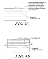
- FIGS. 4A-4D are block diagrams showing the process sequence utilizing the gate structure for a buried channel device (the process is shown for a structure without an optional strained surface layer) using the initial Si/SiGe heterostructure 214 shown in FIG. 2 B.
- the process steps are identical to those of FIGS. 3A-3D, but in the final heterostructure, the Si channel layer 222 is separated from the gate dielectric 400 by a SiGe spacer layer 220 , thus forming a buried channel.
- Using selective processes to etch down to the buried Si channel or the top Si layer can use the starting heterostructure 214 in FIG. 4A to form a surface channel device.
- Such a process can result in enhancement mode and depletion mode devices that can in turn be used to create E/D logic circuits as well as a plethora of analog circuits.
- an exemplary sequence of steps is: 1. Pre-gate-oxidation cleaning steps and oxidation; 2. Selective etch or oxidation to remove residual protective SiGe layer; 3. Sacrificial oxide formation on Si; 4. Sacrificial oxide strip; 5. Gate oxidation.
- steps 3 and 4 can be optional, depending on whether there may be a small amount of Ge left on the surface after the selective removal of the SiGe protection layer.
- the SiGe/Si interface will not be infinitely abrupt, and therefore it is possible to have a small amount of Ge in the optimally pure Si layer.
- a sacrificial oxide step can be employed to remove an additional small amount of the Si layer to ensure that pure Si is oxidized in the gate oxidation step, ensuring high quality gate oxide.
- the second step can be accomplished in a variety of ways.
- One convenient process is a wet oxidation step, preferably at 750° C. or below. Under wet oxidation at these temperatures, SiGe is oxidized at rates that can be 100 times greater than rates oxidizing Si under the same conditions.
- SiGe is oxidized at rates that can be 100 times greater than rates oxidizing Si under the same conditions.
- a wet oxidation step preferably at 750° C. or below.
- SiGe is oxidized at rates that can be 100 times greater than rates oxidizing Si under the same conditions.
- oxidized SiGe can be stripped to expose the Si.
- the low temperature is not only important for the selectivity in the oxidation process, but also the low temperature is important to minimize or prevent the snow-plowing of Ge in front of the oxidation front, a known problem in the direct oxidation of SiGe.
- FIG. 5 is a graph of oxidation rates, under a wet oxidation ambient at 700° C., of SiGe alloys, with Ge contents of 0.28 and 0.36, compared to the oxidation rate of bulk silicon. It is evident from the graph that, under such conditions, the oxidation rate of SiGe increases as the Ge content of the film increases.
- FIG. 6 is a similar graph, showing the oxide thickness of both a Si 0.7 Ge 0.3 alloy and a Si/Si 0.7 Ge 0.3 heterostructure. Again, the oxidation conditions were 700° C. in a wet ambient; however, FIG. 6 depicts very short oxidation durations compared to FIG. 5 .
- the Si/Si 0.7 Ge 0.3 heterostructure consists of a 50 ⁇ strained Si buried layer, followed by a 30 ⁇ Si 0.7 Ge 0.3 , a 20 ⁇ strained Si layer and finally a 50 ⁇ Si 0.7 Ge 0.3 capping layer.
- FIG. 7 A cross-sectional transmission electron micrograph (XTEM) of the Si/Si 0.7 Ge 0.3 heterostructure is shown in FIG. 7 . It should be noted from FIG. 6 that the presence of strained Si layers in the heterostructure results in a dramatic retardation in the oxidation rate when compared to the oxidation rate of the uniform Si 0.7 Ge 0.3 . This retardation of the oxidation rate forms the basis of the selective removal of SiGe alloys over strained Si epitaxial layers.
- FIG. 8 is a XTEM image of the identical Si/Si 0.7 Ge 0.3 heterostructure after wet oxidation at 700° C. for 2 minutes followed by oxide removal via a wet etch. It is apparent that the thin strained Si layer is unaffected by the selective oxidation and remains fully intact. Based on the data shown in FIG. 5, an oxidation duration of 2 minutes far exceeds that required to fully oxidize the 50 ⁇ Si 0.7 Ge 0.3 capping layer of the heterostructure.
- the very thin dark band which is apparent on the surface of the strained Si layer, is a snow-plowed high Ge content layer that occurs during oxidation.
- Such a layer may be removed using a simple chemical clean or a sacrificial oxidation step, either or both of which typically occur prior to the formation of the gate oxide.
- the protective SiGe capping layer can be removed via selective dry or wet chemical etching techniques. For example, at high pressures (>200 mT) and low powers, CF 4 dry etch chemistries will etch relaxed SiGe films with high selectivity to Si. Mixtures of hydrofluoric acid (HF), hydrogen peroxide (H 2 O 2 ), and acetic acid (CH 3 COOH) will also selectively etch relaxed SiGe layers over Si at selectivities of 300:1 or more. Other potential selective wet chemical mixtures include HF, water (H 2 O), and either H 2 O 2 or nitric acid (HNO 3 ).
- HF hydrofluoric acid
- H 2 O 2 hydrogen peroxide
- CH 3 COOH acetic acid
- the stability of the entire structure can be improved by increasing the Ge concentration in the intermediate SiGe layer, and also the top SiGe layer if desired.
- energetic calculations are used to reveal a guide to creating semiconductor layer structures that increase stability with respect to misfit dislocation introduction.
- the critical thickness for a buried channel MOSFET using relaxed SiGe and strained Si has been determined using the energy-balance formulation.
- the structure considered is the one shown in FIG. 9 .
- the structure 900 includes a 30% SiGe virtual substrate 902 topped by a 80 ⁇ strained Si layer 904 , a SiGe layer with Ge concentration x2 and thickness h2 906 , and an additional 30 ⁇ of strained Si 908 . Additional stability would result from the addition of an additional SiGe cap layer as described previously.
- the example of FIG. 9 considers only the increased stability created by increasing the Ge concentration (x2) or thickness (h2) of the SiGe intermediate layer. Additionally, since the SiGe cap layer is removed during processing, the stability of the heterostructure with the SiGe cap removed is or primary importance.
- the dislocation array energy is the same expression regardless of the layer structure.
- the elastic energy in the individual layers is changed because of ⁇ . In tensile layers, the strain is lowered by ⁇ . In compressive layers, the energy is raised by ⁇ .
- the energy for a dislocation array (per unit area) inserted at the base of the composite is:
- h T is the total thickness of the composite (h 1 +h 2 +h 3 )
- ⁇ is the angle between the dislocation line and the Burgers vector b
- v is the Poisson ratio
- D is the average shear modulus for a dislocation lying at the interface between the virtual substrate and the composite structure.
- the energy can now be minimized with respect to ⁇ (if the energy is lowest with no dislocations, then ⁇ will have a less than or equal to zero value).
- h T ⁇ i n ⁇ ⁇ h i .
- FIG. 10 is a graph showing a plot of the middle SiGe layer thickness (h 2 ) and the resulting misfit dislocation spacing.
- the sharp upturn on the plots represents the critical thickness h 2 of the middle SiGe layer when the entire composite structure destabilizes and introduces dislocations at the channel/virtual buffer interface.
- the different curves are for the different compositions in the second layer h 2 .
- Very small increases in Ge result in a large jump in stability of the device layers. This suggests that it is possible to stabilize the layer significantly but not have the band structure altered that much. Adding an extra 5-10% Ge into the h 2 layer increases the stability drastically.
- FIG. 10 indicates that over 100 ⁇ of 30% Ge is required to provide the stability of a 20 ⁇ layer of 45% Ge content.
- Sacrificial SiGe capping layers provide an innovative method for the protection of thin strained device layers during processing. Such layers shield these critically important strained channel layers from process steps, such as wet chemical cleans and oxidations, which consume surface material. Before the growth or deposition of the gate dielectric, these protective SiGe layers can be selectively removed by standard processes such as oxidation or wet etching, revealing the intact strained device layer. Also presented is a guideline for engineering strained layer stacks such that relaxation via misfit dislocation is prevented. Compressively strained intermediate layers increase the stability of tensile channel layers, and also serve as a barrier for misfit dislocation introduction into the underlying layers.
Abstract
Description


Claims (25)
Priority Applications (4)
| Application Number | Priority Date | Filing Date | Title |
|---|---|---|---|
| US09/923,207 US6583015B2 (en) | 2000-08-07 | 2001-08-06 | Gate technology for strained surface channel and strained buried channel MOSFET devices |
| US10/421,154 US6846715B2 (en) | 2000-08-07 | 2003-04-23 | Gate technology for strained surface channel and strained buried channel MOSFET devices |
| US11/013,838 US7217668B2 (en) | 2000-08-07 | 2004-12-16 | Gate technology for strained surface channel and strained buried channel MOSFET devices |
| US11/520,175 US20070082470A1 (en) | 2000-08-07 | 2006-09-13 | Gate technology for strained surface channel and strained buried channel MOSFET devices |
Applications Claiming Priority (2)
| Application Number | Priority Date | Filing Date | Title |
|---|---|---|---|
| US22359500P | 2000-08-07 | 2000-08-07 | |
| US09/923,207 US6583015B2 (en) | 2000-08-07 | 2001-08-06 | Gate technology for strained surface channel and strained buried channel MOSFET devices |
Related Child Applications (1)
| Application Number | Title | Priority Date | Filing Date |
|---|---|---|---|
| US10/421,154 Continuation US6846715B2 (en) | 2000-08-07 | 2003-04-23 | Gate technology for strained surface channel and strained buried channel MOSFET devices |
Publications (2)
| Publication Number | Publication Date |
|---|---|
| US20020068393A1 US20020068393A1 (en) | 2002-06-06 |
| US6583015B2 true US6583015B2 (en) | 2003-06-24 |
Family
ID=22837179
Family Applications (5)
| Application Number | Title | Priority Date | Filing Date |
|---|---|---|---|
| US09/922,822 Abandoned US20020104993A1 (en) | 2000-08-07 | 2001-08-06 | Gate technology for strained surface channel and strained buried channel MOSFET devices |
| US09/923,207 Expired - Lifetime US6583015B2 (en) | 2000-08-07 | 2001-08-06 | Gate technology for strained surface channel and strained buried channel MOSFET devices |
| US10/421,154 Expired - Lifetime US6846715B2 (en) | 2000-08-07 | 2003-04-23 | Gate technology for strained surface channel and strained buried channel MOSFET devices |
| US11/013,838 Expired - Lifetime US7217668B2 (en) | 2000-08-07 | 2004-12-16 | Gate technology for strained surface channel and strained buried channel MOSFET devices |
| US11/520,175 Abandoned US20070082470A1 (en) | 2000-08-07 | 2006-09-13 | Gate technology for strained surface channel and strained buried channel MOSFET devices |
Family Applications Before (1)
| Application Number | Title | Priority Date | Filing Date |
|---|---|---|---|
| US09/922,822 Abandoned US20020104993A1 (en) | 2000-08-07 | 2001-08-06 | Gate technology for strained surface channel and strained buried channel MOSFET devices |
Family Applications After (3)
| Application Number | Title | Priority Date | Filing Date |
|---|---|---|---|
| US10/421,154 Expired - Lifetime US6846715B2 (en) | 2000-08-07 | 2003-04-23 | Gate technology for strained surface channel and strained buried channel MOSFET devices |
| US11/013,838 Expired - Lifetime US7217668B2 (en) | 2000-08-07 | 2004-12-16 | Gate technology for strained surface channel and strained buried channel MOSFET devices |
| US11/520,175 Abandoned US20070082470A1 (en) | 2000-08-07 | 2006-09-13 | Gate technology for strained surface channel and strained buried channel MOSFET devices |
Country Status (5)
| Country | Link |
|---|---|
| US (5) | US20020104993A1 (en) |
| EP (1) | EP1307917A2 (en) |
| JP (1) | JP2004519090A (en) |
| AU (1) | AU2001283138A1 (en) |
| WO (1) | WO2002013262A2 (en) |
Cited By (57)
| Publication number | Priority date | Publication date | Assignee | Title |
|---|---|---|---|---|
| US20030034529A1 (en) * | 2000-12-04 | 2003-02-20 | Amberwave Systems Corporation | CMOS inverter and integrated circuits utilizing strained silicon surface channel MOSFETs |
| US20030102498A1 (en) * | 2001-09-24 | 2003-06-05 | Glyn Braithwaite | RF circuits including transistors having strained material layers |
| US20030113948A1 (en) * | 2000-01-20 | 2003-06-19 | Amberwave Systems Corporation | Low threading dislocation density relaxed mismatched epilayers without high temperature growth |
| US20040000268A1 (en) * | 1998-04-10 | 2004-01-01 | Massachusetts Institute Of Technology | Etch stop layer system |
| US6703144B2 (en) | 2000-01-20 | 2004-03-09 | Amberwave Systems Corporation | Heterointegration of materials using deposition and bonding |
| US20040075105A1 (en) * | 2002-08-23 | 2004-04-22 | Amberwave Systems Corporation | Semiconductor heterostructures having reduced dislocation pile-ups and related methods |
| US6730576B1 (en) * | 2002-12-31 | 2004-05-04 | Advanced Micro Devices, Inc. | Method of forming a thick strained silicon layer and semiconductor structures incorporating a thick strained silicon layer |
| US20040084668A1 (en) * | 2002-07-08 | 2004-05-06 | Amberwave Systems Corporation | Back-biasing to populate strained layer quantum wells |
| US20040171223A1 (en) * | 2001-06-14 | 2004-09-02 | Amberwave Systems Corporation | Method of selective removal of SiGe alloys |
| US20040206950A1 (en) * | 2003-04-18 | 2004-10-21 | Agajan Suvkhanov | Ion recoil implantation and enhanced carrier mobility in CMOS device |
| US20040206951A1 (en) * | 2003-04-18 | 2004-10-21 | Mirabedini Mohammad R. | Ion implantation in channel region of CMOS device for enhanced carrier mobility |
| US20040235274A1 (en) * | 2003-05-19 | 2004-11-25 | Toshiba Ceramics Co., Ltd. | Manufacturing method for a silicon substrate having strained layer |
| US20040262631A1 (en) * | 1997-06-24 | 2004-12-30 | Massachusetts Institute Of Technology | Controlling threading dislocation densities in Ge on Si using graded GeSi layers and planarization |
| US20040262694A1 (en) * | 2003-06-25 | 2004-12-30 | Chidambaram Pr | Transistor device containing carbon doped silicon in a recess next to MDD to create strain in channel |
| US20050006565A1 (en) * | 2003-07-07 | 2005-01-13 | Chandra Mouli | Pixel with strained silicon layer for improving carrier mobility and blue response in imagers |
| US20050082567A1 (en) * | 2003-10-16 | 2005-04-21 | Industrial Technology Research Institute | Structure of a relaxed Si/Ge epitaxial layer and fabricating method thereof |
| US20050130424A1 (en) * | 2002-07-16 | 2005-06-16 | International Business Machines Corporation | Use of hydrogen implantation to improve material properties of silicon-germanium-on-insulator material made by thermal diffusion |
| US20050127138A1 (en) * | 2003-12-15 | 2005-06-16 | Isabelle Bacon | Compressor rotor and method for making |
| US20050139872A1 (en) * | 2003-12-31 | 2005-06-30 | Chidambaram Pr | Drive current improvement from recessed SiGe incorporation close to gate |
| US20050164436A1 (en) * | 2004-01-23 | 2005-07-28 | Chartered Semiconductor Manufacturing Ltd. | Method of forming a relaxed semiconductor buffer layer on a substrate with a large lattice mismatch |
| US20050164473A1 (en) * | 2004-01-23 | 2005-07-28 | Chartered Semiconductor Manufacturing Ltd. | Method of forming a relaxed semiconductor buffer layer on a substrate with a large lattice mismatch |
| US20050164477A1 (en) * | 2003-09-23 | 2005-07-28 | Dureseti Chidambarrao | Strained silicon on relaxed sige film with uniform misfit dislocation density |
| US20050169096A1 (en) * | 2003-07-01 | 2005-08-04 | Lee Hyo-San | PAA- based etchant, methods of using same, and resultant structures |
| US20050191795A1 (en) * | 2004-03-01 | 2005-09-01 | Dureseti Chidambarrao | Method of manufacture of FinFET devices with T-shaped fins and devices manufactured thereby |
| US20050195012A1 (en) * | 2004-03-02 | 2005-09-08 | Atsushi Sueoka | Semiconductor device |
| US6946371B2 (en) | 2002-06-10 | 2005-09-20 | Amberwave Systems Corporation | Methods of fabricating semiconductor structures having epitaxially grown source and drain elements |
| US20050214997A1 (en) * | 2004-03-23 | 2005-09-29 | Sharp Laboratories Of America, Inc. | Method to form local "silicon-on-nothing" or "silicon-on-insulator" wafers with tensile-strained silicon |
| US20060024898A1 (en) * | 2004-07-29 | 2006-02-02 | Chidambaram Pr | Increased drive current by isotropic recess etch |
| US20060030527A1 (en) * | 2004-08-03 | 2006-02-09 | Mjalli Adnan M | Rage fusion proteins and methods of use |
| US20060205194A1 (en) * | 2005-02-04 | 2006-09-14 | Matthias Bauer | Methods of depositing electrically active doped crystalline Si-containing films |
| US20070082470A1 (en) * | 2000-08-07 | 2007-04-12 | Amberwave System Corporation | Gate technology for strained surface channel and strained buried channel MOSFET devices |
| US7224007B1 (en) * | 2004-01-12 | 2007-05-29 | Advanced Micro Devices, Inc. | Multi-channel transistor with tunable hot carrier effect |
| US20070161216A1 (en) * | 2005-12-22 | 2007-07-12 | Matthias Bauer | Epitaxial deposition of doped semiconductor materials |
| US20080073645A1 (en) * | 2001-02-12 | 2008-03-27 | Asm America, Inc. | Thin films and methods of making them |
| US20080142842A1 (en) * | 2002-08-27 | 2008-06-19 | Taiwan Semiconductor Manufacturing Company, Ltd. | Relaxed silicon germanium substrate with low defect density |
| US20090075029A1 (en) * | 2007-09-19 | 2009-03-19 | Asm America, Inc. | Stressor for engineered strain on channel |
| US20090111246A1 (en) * | 2007-10-26 | 2009-04-30 | Asm America, Inc. | Inhibitors for selective deposition of silicon containing films |
| US20090163001A1 (en) * | 2007-12-21 | 2009-06-25 | Asm America, Inc. | Separate injection of reactive species in selective formation of films |
| US7776697B2 (en) | 2001-09-21 | 2010-08-17 | Taiwan Semiconductor Manufacturing Company, Ltd. | Semiconductor structures employing strained material layers with defined impurity gradients and methods for fabricating same |
| US20100255658A1 (en) * | 2009-04-07 | 2010-10-07 | Asm America, Inc. | Substrate reactor with adjustable injectors for mixing gases within reaction chamber |
| US7838392B2 (en) | 2002-06-07 | 2010-11-23 | Taiwan Semiconductor Manufacturing Company, Ltd. | Methods for forming III-V semiconductor device structures |
| US20110068403A1 (en) * | 2004-12-17 | 2011-03-24 | Hattendorf Michael L | Strained nmos transistor featuring deep carbon doped regions and raised donor doped source and drain |
| US8129821B2 (en) | 2002-06-25 | 2012-03-06 | Taiwan Semiconductor Manufacturing Co., Ltd. | Reacted conductive gate electrodes |
| US8183627B2 (en) | 2004-12-01 | 2012-05-22 | Taiwan Semiconductor Manufacturing Company, Ltd. | Hybrid fin field-effect transistor structures and related methods |
| US8278176B2 (en) | 2006-06-07 | 2012-10-02 | Asm America, Inc. | Selective epitaxial formation of semiconductor films |
| US8367528B2 (en) | 2009-11-17 | 2013-02-05 | Asm America, Inc. | Cyclical epitaxial deposition and etch |
| US8748292B2 (en) | 2002-06-07 | 2014-06-10 | Taiwan Semiconductor Manufacturing Company, Ltd. | Methods of forming strained-semiconductor-on-insulator device structures |
| CN103940885A (en) * | 2014-03-18 | 2014-07-23 | 复旦大学 | Ion sensitive field effect transistor and preparation process thereof |
| US8809170B2 (en) | 2011-05-19 | 2014-08-19 | Asm America Inc. | High throughput cyclical epitaxial deposition and etch process |
| US8822282B2 (en) | 2001-03-02 | 2014-09-02 | Taiwan Semiconductor Manufacturing Company, Ltd. | Methods of fabricating contact regions for FET incorporating SiGe |
| US8921205B2 (en) | 2002-08-14 | 2014-12-30 | Asm America, Inc. | Deposition of amorphous silicon-containing films |
| US8928096B2 (en) | 2012-05-14 | 2015-01-06 | International Business Machines Corporation | Buried-channel field-effect transistors |
| US9041062B2 (en) | 2013-09-19 | 2015-05-26 | International Business Machines Corporation | Silicon-on-nothing FinFETs |
| US20160240613A1 (en) * | 2014-11-19 | 2016-08-18 | International Business Machines Corporation | Iii-v semiconductor devices with selective oxidation |
| US9443953B1 (en) | 2015-08-24 | 2016-09-13 | International Business Machines Corporation | Sacrificial silicon germanium channel for inversion oxide thickness scaling with mitigated work function roll-off and improved negative bias temperature instability |
| US20170317103A1 (en) * | 2016-04-28 | 2017-11-02 | Globalfoundries Singapore Pte. Ltd. | Integrated circuits with selectively strained device regions and methods for fabricating same |
| US9899274B2 (en) | 2015-03-16 | 2018-02-20 | International Business Machines Corporation | Low-cost SOI FinFET technology |
Families Citing this family (40)
| Publication number | Priority date | Publication date | Assignee | Title |
|---|---|---|---|---|
| JP2004507084A (en) | 2000-08-16 | 2004-03-04 | マサチューセッツ インスティテュート オブ テクノロジー | Manufacturing process of semiconductor products using graded epitaxial growth |
| US6649480B2 (en) | 2000-12-04 | 2003-11-18 | Amberwave Systems Corporation | Method of fabricating CMOS inverter and integrated circuits utilizing strained silicon surface channel MOSFETs |
| WO2002071493A2 (en) * | 2001-03-02 | 2002-09-12 | Amberwave Systems Corporation | Relaxed silicon germanium platform for high speed cmos electronics and high speed analog |
| US6900103B2 (en) | 2001-03-02 | 2005-05-31 | Amberwave Systems Corporation | Relaxed silicon germanium platform for high speed CMOS electronics and high speed analog circuits |
| WO2002071488A1 (en) * | 2001-03-02 | 2002-09-12 | Amberwave Systems Corporation | Relaxed silicon germanium platform for high speed cmos electronics and high speed analog circuits |
| US6593641B1 (en) * | 2001-03-02 | 2003-07-15 | Amberwave Systems Corporation | Relaxed silicon germanium platform for high speed CMOS electronics and high speed analog circuits |
| US6723661B2 (en) * | 2001-03-02 | 2004-04-20 | Amberwave Systems Corporation | Relaxed silicon germanium platform for high speed CMOS electronics and high speed analog circuits |
| US6724008B2 (en) | 2001-03-02 | 2004-04-20 | Amberwave Systems Corporation | Relaxed silicon germanium platform for high speed CMOS electronics and high speed analog circuits |
| US6703688B1 (en) | 2001-03-02 | 2004-03-09 | Amberwave Systems Corporation | Relaxed silicon germanium platform for high speed CMOS electronics and high speed analog circuits |
| US6646322B2 (en) | 2001-03-02 | 2003-11-11 | Amberwave Systems Corporation | Relaxed silicon germanium platform for high speed CMOS electronics and high speed analog circuits |
| WO2003001671A2 (en) | 2001-06-21 | 2003-01-03 | Amberwave Systems Corporation | Improved enhancement of p-type metal-oxide-semiconductor field-effect transistors |
| US6730551B2 (en) | 2001-08-06 | 2004-05-04 | Massachusetts Institute Of Technology | Formation of planar strained layers |
| US6974735B2 (en) | 2001-08-09 | 2005-12-13 | Amberwave Systems Corporation | Dual layer Semiconductor Devices |
| US7138649B2 (en) | 2001-08-09 | 2006-11-21 | Amberwave Systems Corporation | Dual-channel CMOS transistors with differentially strained channels |
| JP3970011B2 (en) * | 2001-12-11 | 2007-09-05 | シャープ株式会社 | Semiconductor device and manufacturing method thereof |
| WO2003079415A2 (en) * | 2002-03-14 | 2003-09-25 | Amberwave Systems Corporation | Methods for fabricating strained layers on semiconductor substrates |
| US7138310B2 (en) | 2002-06-07 | 2006-11-21 | Amberwave Systems Corporation | Semiconductor devices having strained dual channel layers |
| US6646318B1 (en) * | 2002-08-15 | 2003-11-11 | National Semiconductor Corporation | Bandgap tuned vertical color imager cell |
| US20040137698A1 (en) * | 2002-08-29 | 2004-07-15 | Gianni Taraschi | Fabrication system and method for monocrystaline semiconductor on a substrate |
| JP4949628B2 (en) * | 2002-10-30 | 2012-06-13 | 台湾積體電路製造股▲ふん▼有限公司 | Method for protecting a strained semiconductor substrate layer during a CMOS process |
| US6963078B2 (en) * | 2003-03-15 | 2005-11-08 | International Business Machines Corporation | Dual strain-state SiGe layers for microelectronics |
| US7026249B2 (en) * | 2003-05-30 | 2006-04-11 | International Business Machines Corporation | SiGe lattice engineering using a combination of oxidation, thinning and epitaxial regrowth |
| US6803240B1 (en) * | 2003-09-03 | 2004-10-12 | International Business Machines Corporation | Method of measuring crystal defects in thin Si/SiGe bilayers |
| US6955932B2 (en) * | 2003-10-29 | 2005-10-18 | International Business Machines Corporation | Single and double-gate pseudo-FET devices for semiconductor materials evaluation |
| FR2872626B1 (en) * | 2004-07-05 | 2008-05-02 | Commissariat Energie Atomique | METHOD FOR CONTRAINDING A THIN PATTERN |
| US20060105559A1 (en) * | 2004-11-15 | 2006-05-18 | International Business Machines Corporation | Ultrathin buried insulators in Si or Si-containing material |
| US7547605B2 (en) * | 2004-11-22 | 2009-06-16 | Taiwan Semiconductor Manufacturing Company | Microelectronic device and a method for its manufacture |
| US20060234455A1 (en) * | 2005-04-19 | 2006-10-19 | Chien-Hao Chen | Structures and methods for forming a locally strained transistor |
| JP2007036134A (en) * | 2005-07-29 | 2007-02-08 | Toshiba Corp | Semiconductor wafer and method for manufacturing semiconductor device |
| US7348225B2 (en) * | 2005-10-27 | 2008-03-25 | International Business Machines Corporation | Structure and method of fabricating FINFET with buried channel |
| US20070105516A1 (en) * | 2005-11-10 | 2007-05-10 | Hickman Barton T | Automatic compensation of gain versus temperature |
| US8900980B2 (en) | 2006-01-20 | 2014-12-02 | Taiwan Semiconductor Manufacturing Company, Ltd. | Defect-free SiGe source/drain formation by epitaxy-free process |
| US9252981B2 (en) * | 2006-06-13 | 2016-02-02 | At&T Intellectual Property I, L.P. | Method and apparatus for processing a communication request from a roaming voice over IP terminal |
| US7989901B2 (en) * | 2007-04-27 | 2011-08-02 | Taiwan Semiconductor Manufacturing Company, Ltd. | MOS devices with improved source/drain regions with SiGe |
| FR2921515B1 (en) * | 2007-09-25 | 2010-07-30 | Commissariat Energie Atomique | METHOD FOR MANUFACTURING SEMICONDUCTOR STRUCTURES USEFUL FOR PRODUCING SEMICONDUCTOR-OVER-INSULATING SUBSTRATES, AND APPLICATIONS THEREOF |
| US8453913B2 (en) | 2009-02-06 | 2013-06-04 | Covidien Lp | Anvil for surgical stapler |
| KR20180068591A (en) | 2016-12-14 | 2018-06-22 | 삼성전자주식회사 | Etching composition and method for fabricating semiconductor device by using the same |
| JP6886042B2 (en) * | 2017-04-11 | 2021-06-16 | インテグリス・インコーポレーテッド | Formulation for selectively etching silicon germanium against silicon |
| KR102480348B1 (en) | 2018-03-15 | 2022-12-23 | 삼성전자주식회사 | Pre-treatment composition before etching SiGe and method of fabricating a semiconductor device |
| CN109950153B (en) * | 2019-03-08 | 2022-03-04 | 中国科学院微电子研究所 | Semiconductor structure and manufacturing method thereof |
Citations (17)
| Publication number | Priority date | Publication date | Assignee | Title |
|---|---|---|---|---|
| US5166084A (en) * | 1991-09-03 | 1992-11-24 | Motorola, Inc. | Process for fabricating a silicon on insulator field effect transistor |
| US5212110A (en) * | 1992-05-26 | 1993-05-18 | Motorola, Inc. | Method for forming isolation regions in a semiconductor device |
| EP0587520A1 (en) | 1992-08-10 | 1994-03-16 | International Business Machines Corporation | A SiGe thin film or SOI MOSFET and method for making the same |
| EP0683522A2 (en) | 1994-05-20 | 1995-11-22 | International Business Machines Corporation | CMOS with strained Si/SiGe layers |
| JP2000031491A (en) | 1998-07-14 | 2000-01-28 | Hitachi Ltd | Semiconductor device, its manufacture, semiconductor substrate and its manufacture |
| US6074919A (en) | 1999-01-20 | 2000-06-13 | Advanced Micro Devices, Inc. | Method of forming an ultrathin gate dielectric |
| US6096590A (en) | 1996-07-18 | 2000-08-01 | International Business Machines Corporation | Scalable MOS field effect transistor |
| US6103559A (en) | 1999-03-30 | 2000-08-15 | Amd, Inc. (Advanced Micro Devices) | Method of making disposable channel masking for both source/drain and LDD implant and subsequent gate fabrication |
| US6111267A (en) * | 1997-05-13 | 2000-08-29 | Siemens Aktiengesellschaft | CMOS integrated circuit including forming doped wells, a layer of intrinsic silicon, a stressed silicon germanium layer where germanium is between 25 and 50%, and another intrinsic silicon layer |
| US6154475A (en) * | 1997-12-04 | 2000-11-28 | The United States Of America As Represented By The Secretary Of The Air Force | Silicon-based strain-symmetrized GE-SI quantum lasers |
| US6162688A (en) | 1999-01-14 | 2000-12-19 | Advanced Micro Devices, Inc. | Method of fabricating a transistor with a dielectric underlayer and device incorporating same |
| US6191432B1 (en) * | 1996-09-02 | 2001-02-20 | Kabushiki Kaisha Toshiba | Semiconductor device and memory device |
| US6194722B1 (en) | 1997-03-28 | 2001-02-27 | Interuniversitair Micro-Elektronica Centrum, Imec, Vzw | Method of fabrication of an infrared radiation detector and infrared detector device |
| US6207977B1 (en) * | 1995-06-16 | 2001-03-27 | Interuniversitaire Microelektronica | Vertical MISFET devices |
| US6210988B1 (en) | 1999-01-15 | 2001-04-03 | The Regents Of The University Of California | Polycrystalline silicon germanium films for forming micro-electromechanical systems |
| US6218677B1 (en) * | 1994-08-15 | 2001-04-17 | Texas Instruments Incorporated | III-V nitride resonant tunneling |
| US6350993B1 (en) * | 1999-03-12 | 2002-02-26 | International Business Machines Corporation | High speed composite p-channel Si/SiGe heterostructure for field effect devices |
Family Cites Families (65)
| Publication number | Priority date | Publication date | Assignee | Title |
|---|---|---|---|---|
| DE3542482A1 (en) * | 1985-11-30 | 1987-06-04 | Licentia Gmbh | MODULATION-Doped FIELD EFFECT TRANSISTOR |
| US4920076A (en) * | 1988-04-15 | 1990-04-24 | The United States Of America As Represented By The United States Department Of Energy | Method for enhancing growth of SiO2 in Si by the implantation of germanium |
| DE3816358A1 (en) * | 1988-05-13 | 1989-11-23 | Eurosil Electronic Gmbh | NON-VOLATILE STORAGE CELL AND METHOD FOR THE PRODUCTION THEREOF |
| US4958318A (en) * | 1988-07-08 | 1990-09-18 | Eliyahou Harari | Sidewall capacitor DRAM cell |
| US5241197A (en) * | 1989-01-25 | 1993-08-31 | Hitachi, Ltd. | Transistor provided with strained germanium layer |
| US5312766A (en) * | 1991-03-06 | 1994-05-17 | National Semiconductor Corporation | Method of providing lower contact resistance in MOS transistors |
| US5442205A (en) * | 1991-04-24 | 1995-08-15 | At&T Corp. | Semiconductor heterostructure devices with strained semiconductor layers |
| US5291439A (en) * | 1991-09-12 | 1994-03-01 | International Business Machines Corporation | Semiconductor memory cell and memory array with inversion layer |
| JPH05121317A (en) * | 1991-10-24 | 1993-05-18 | Rohm Co Ltd | Method for forming soi structure |
| US5467305A (en) * | 1992-03-12 | 1995-11-14 | International Business Machines Corporation | Three-dimensional direct-write EEPROM arrays and fabrication methods |
| US5386132A (en) * | 1992-11-02 | 1995-01-31 | Wong; Chun C. D. | Multimedia storage system with highly compact memory device |
| US5418743A (en) * | 1992-12-07 | 1995-05-23 | Nippon Steel Corporation | Method of writing into non-volatile semiconductor memory |
| US5523592A (en) * | 1993-02-03 | 1996-06-04 | Hitachi, Ltd. | Semiconductor optical device, manufacturing method for the same, and opto-electronic integrated circuit using the same |
| US5792679A (en) * | 1993-08-30 | 1998-08-11 | Sharp Microelectronics Technology, Inc. | Method for forming silicon-germanium/Si/silicon dioxide heterostructure using germanium implant |
| US5461243A (en) * | 1993-10-29 | 1995-10-24 | International Business Machines Corporation | Substrate for tensilely strained semiconductor |
| US5561302A (en) * | 1994-09-26 | 1996-10-01 | Motorola, Inc. | Enhanced mobility MOSFET device and method |
| US5777347A (en) * | 1995-03-07 | 1998-07-07 | Hewlett-Packard Company | Vertical CMOS digital multi-valued restoring logic device |
| DE19533313A1 (en) * | 1995-09-08 | 1997-03-13 | Max Planck Gesellschaft | Semiconductor transistor device structure for e.g. CMOS FET |
| JP3403877B2 (en) * | 1995-10-25 | 2003-05-06 | 三菱電機株式会社 | Semiconductor memory device and manufacturing method thereof |
| US5847419A (en) * | 1996-09-17 | 1998-12-08 | Kabushiki Kaisha Toshiba | Si-SiGe semiconductor device and method of fabricating the same |
| US6399970B2 (en) * | 1996-09-17 | 2002-06-04 | Matsushita Electric Industrial Co., Ltd. | FET having a Si/SiGeC heterojunction channel |
| EP0838858B1 (en) * | 1996-09-27 | 2002-05-15 | Infineon Technologies AG | CMOS integrated circuit and method of manufacturing the same |
| US5780922A (en) * | 1996-11-27 | 1998-07-14 | The Regents Of The University Of California | Ultra-low phase noise GE MOSFETs |
| US5808344A (en) * | 1996-12-13 | 1998-09-15 | International Business Machines Corporation | Single-transistor logic and CMOS inverters |
| US5891769A (en) * | 1997-04-07 | 1999-04-06 | Motorola, Inc. | Method for forming a semiconductor device having a heteroepitaxial layer |
| US5906951A (en) * | 1997-04-30 | 1999-05-25 | International Business Machines Corporation | Strained Si/SiGe layers on insulator |
| WO1998059365A1 (en) * | 1997-06-24 | 1998-12-30 | Massachusetts Institute Of Technology | CONTROLLING THREADING DISLOCATION DENSITIES IN Ge ON Si USING GRADED GeSi LAYERS AND PLANARIZATION |
| US5936274A (en) * | 1997-07-08 | 1999-08-10 | Micron Technology, Inc. | High density flash memory |
| US5981400A (en) * | 1997-09-18 | 1999-11-09 | Cornell Research Foundation, Inc. | Compliant universal substrate for epitaxial growth |
| US5963817A (en) * | 1997-10-16 | 1999-10-05 | International Business Machines Corporation | Bulk and strained silicon on insulator using local selective oxidation |
| JP3447939B2 (en) * | 1997-12-10 | 2003-09-16 | 株式会社東芝 | Nonvolatile semiconductor memory and data reading method |
| FR2773177B1 (en) * | 1997-12-29 | 2000-03-17 | France Telecom | PROCESS FOR OBTAINING A SINGLE-CRYSTAL GERMANIUM OR SILICON LAYER ON A SILICON OR SINGLE-CRYSTAL GERMANIUM SUBSTRATE, RESPECTIVELY, AND MULTILAYER PRODUCTS OBTAINED |
| US6013134A (en) * | 1998-02-18 | 2000-01-11 | International Business Machines Corporation | Advance integrated chemical vapor deposition (AICVD) for semiconductor devices |
| US6689211B1 (en) * | 1999-04-09 | 2004-02-10 | Massachusetts Institute Of Technology | Etch stop layer system |
| JP4258034B2 (en) * | 1998-05-27 | 2009-04-30 | ソニー株式会社 | Semiconductor device and manufacturing method of semiconductor device |
| JP3403076B2 (en) * | 1998-06-30 | 2003-05-06 | 株式会社東芝 | Semiconductor device and manufacturing method thereof |
| US6130453A (en) * | 1999-01-04 | 2000-10-10 | International Business Machines Corporation | Flash memory structure with floating gate in vertical trench |
| JP3595718B2 (en) * | 1999-03-15 | 2004-12-02 | 株式会社東芝 | Display element and method of manufacturing the same |
| US6251755B1 (en) * | 1999-04-22 | 2001-06-26 | International Business Machines Corporation | High resolution dopant/impurity incorporation in semiconductors via a scanned atomic force probe |
| US6151248A (en) * | 1999-06-30 | 2000-11-21 | Sandisk Corporation | Dual floating gate EEPROM cell array with steering gates shared by adjacent cells |
| US6204529B1 (en) * | 1999-08-27 | 2001-03-20 | Hsing Lan Lung | 8 bit per cell non-volatile semiconductor memory structure utilizing trench technology and dielectric floating gate |
| US6339232B1 (en) * | 1999-09-20 | 2002-01-15 | Kabushika Kaisha Toshiba | Semiconductor device |
| US6559040B1 (en) * | 1999-10-20 | 2003-05-06 | Taiwan Semiconductor Manufacturing Company | Process for polishing the top surface of a polysilicon gate |
| US6249022B1 (en) * | 1999-10-22 | 2001-06-19 | United Microelectronics Corp. | Trench flash memory with nitride spacers for electron trapping |
| US6551399B1 (en) * | 2000-01-10 | 2003-04-22 | Genus Inc. | Fully integrated process for MIM capacitors using atomic layer deposition |
| DE10025264A1 (en) * | 2000-05-22 | 2001-11-29 | Max Planck Gesellschaft | Field effect transistor based on embedded cluster structures and method for its production |
| JP3546169B2 (en) * | 2000-05-26 | 2004-07-21 | 三菱重工業株式会社 | Semiconductor device and manufacturing method thereof |
| JP2004519090A (en) * | 2000-08-07 | 2004-06-24 | アンバーウェーブ システムズ コーポレイション | Gate technology for strained surface channel and strained buried channel MOSFET devices |
| AU2002228779A1 (en) * | 2000-12-04 | 2002-06-18 | Amberwave Systems Corporation | Cmos inverter circuits utilizing strained silicon surface channel mosfets |
| US6649480B2 (en) * | 2000-12-04 | 2003-11-18 | Amberwave Systems Corporation | Method of fabricating CMOS inverter and integrated circuits utilizing strained silicon surface channel MOSFETs |
| US20020100942A1 (en) * | 2000-12-04 | 2002-08-01 | Fitzgerald Eugene A. | CMOS inverter and integrated circuits utilizing strained silicon surface channel MOSFETs |
| KR100391988B1 (en) * | 2001-02-09 | 2003-07-22 | 삼성전자주식회사 | DRAM cell and fabrication method thereof |
| US6724008B2 (en) * | 2001-03-02 | 2004-04-20 | Amberwave Systems Corporation | Relaxed silicon germanium platform for high speed CMOS electronics and high speed analog circuits |
| US6646322B2 (en) * | 2001-03-02 | 2003-11-11 | Amberwave Systems Corporation | Relaxed silicon germanium platform for high speed CMOS electronics and high speed analog circuits |
| US6723661B2 (en) * | 2001-03-02 | 2004-04-20 | Amberwave Systems Corporation | Relaxed silicon germanium platform for high speed CMOS electronics and high speed analog circuits |
| US6348407B1 (en) * | 2001-03-15 | 2002-02-19 | Chartered Semiconductor Manufacturing Inc. | Method to improve adhesion of organic dielectrics in dual damascene interconnects |
| US6531324B2 (en) * | 2001-03-28 | 2003-03-11 | Sharp Laboratories Of America, Inc. | MFOS memory transistor & method of fabricating same |
| US6603156B2 (en) * | 2001-03-31 | 2003-08-05 | International Business Machines Corporation | Strained silicon on insulator structures |
| US6468869B1 (en) * | 2001-05-11 | 2002-10-22 | Macronix International Co., Ltd. | Method of fabricating mask read only memory |
| AU2002322105A1 (en) * | 2001-06-14 | 2003-01-02 | Amberware Systems Corporation | Method of selective removal of sige alloys |
| US7301180B2 (en) * | 2001-06-18 | 2007-11-27 | Massachusetts Institute Of Technology | Structure and method for a high-speed semiconductor device having a Ge channel layer |
| WO2003001671A2 (en) * | 2001-06-21 | 2003-01-03 | Amberwave Systems Corporation | Improved enhancement of p-type metal-oxide-semiconductor field-effect transistors |
| US6974735B2 (en) * | 2001-08-09 | 2005-12-13 | Amberwave Systems Corporation | Dual layer Semiconductor Devices |
| US6541321B1 (en) * | 2002-05-14 | 2003-04-01 | Advanced Micro Devices, Inc. | Method of making transistors with gate insulation layers of differing thickness |
| US7169226B2 (en) * | 2003-07-01 | 2007-01-30 | International Business Machines Corporation | Defect reduction by oxidation of silicon |
-
2001
- 2001-08-06 JP JP2002518522A patent/JP2004519090A/en active Pending
- 2001-08-06 AU AU2001283138A patent/AU2001283138A1/en not_active Abandoned
- 2001-08-06 US US09/922,822 patent/US20020104993A1/en not_active Abandoned
- 2001-08-06 US US09/923,207 patent/US6583015B2/en not_active Expired - Lifetime
- 2001-08-06 WO PCT/US2001/024614 patent/WO2002013262A2/en active Application Filing
- 2001-08-06 EP EP01961913A patent/EP1307917A2/en not_active Withdrawn
-
2003
- 2003-04-23 US US10/421,154 patent/US6846715B2/en not_active Expired - Lifetime
-
2004
- 2004-12-16 US US11/013,838 patent/US7217668B2/en not_active Expired - Lifetime
-
2006
- 2006-09-13 US US11/520,175 patent/US20070082470A1/en not_active Abandoned
Patent Citations (17)
| Publication number | Priority date | Publication date | Assignee | Title |
|---|---|---|---|---|
| US5166084A (en) * | 1991-09-03 | 1992-11-24 | Motorola, Inc. | Process for fabricating a silicon on insulator field effect transistor |
| US5212110A (en) * | 1992-05-26 | 1993-05-18 | Motorola, Inc. | Method for forming isolation regions in a semiconductor device |
| EP0587520A1 (en) | 1992-08-10 | 1994-03-16 | International Business Machines Corporation | A SiGe thin film or SOI MOSFET and method for making the same |
| EP0683522A2 (en) | 1994-05-20 | 1995-11-22 | International Business Machines Corporation | CMOS with strained Si/SiGe layers |
| US6218677B1 (en) * | 1994-08-15 | 2001-04-17 | Texas Instruments Incorporated | III-V nitride resonant tunneling |
| US6207977B1 (en) * | 1995-06-16 | 2001-03-27 | Interuniversitaire Microelektronica | Vertical MISFET devices |
| US6096590A (en) | 1996-07-18 | 2000-08-01 | International Business Machines Corporation | Scalable MOS field effect transistor |
| US6191432B1 (en) * | 1996-09-02 | 2001-02-20 | Kabushiki Kaisha Toshiba | Semiconductor device and memory device |
| US6194722B1 (en) | 1997-03-28 | 2001-02-27 | Interuniversitair Micro-Elektronica Centrum, Imec, Vzw | Method of fabrication of an infrared radiation detector and infrared detector device |
| US6111267A (en) * | 1997-05-13 | 2000-08-29 | Siemens Aktiengesellschaft | CMOS integrated circuit including forming doped wells, a layer of intrinsic silicon, a stressed silicon germanium layer where germanium is between 25 and 50%, and another intrinsic silicon layer |
| US6154475A (en) * | 1997-12-04 | 2000-11-28 | The United States Of America As Represented By The Secretary Of The Air Force | Silicon-based strain-symmetrized GE-SI quantum lasers |
| JP2000031491A (en) | 1998-07-14 | 2000-01-28 | Hitachi Ltd | Semiconductor device, its manufacture, semiconductor substrate and its manufacture |
| US6162688A (en) | 1999-01-14 | 2000-12-19 | Advanced Micro Devices, Inc. | Method of fabricating a transistor with a dielectric underlayer and device incorporating same |
| US6210988B1 (en) | 1999-01-15 | 2001-04-03 | The Regents Of The University Of California | Polycrystalline silicon germanium films for forming micro-electromechanical systems |
| US6074919A (en) | 1999-01-20 | 2000-06-13 | Advanced Micro Devices, Inc. | Method of forming an ultrathin gate dielectric |
| US6350993B1 (en) * | 1999-03-12 | 2002-02-26 | International Business Machines Corporation | High speed composite p-channel Si/SiGe heterostructure for field effect devices |
| US6103559A (en) | 1999-03-30 | 2000-08-15 | Amd, Inc. (Advanced Micro Devices) | Method of making disposable channel masking for both source/drain and LDD implant and subsequent gate fabrication |
Cited By (118)
| Publication number | Priority date | Publication date | Assignee | Title |
|---|---|---|---|---|
| US20040262631A1 (en) * | 1997-06-24 | 2004-12-30 | Massachusetts Institute Of Technology | Controlling threading dislocation densities in Ge on Si using graded GeSi layers and planarization |
| US20040000268A1 (en) * | 1998-04-10 | 2004-01-01 | Massachusetts Institute Of Technology | Etch stop layer system |
| US20030113948A1 (en) * | 2000-01-20 | 2003-06-19 | Amberwave Systems Corporation | Low threading dislocation density relaxed mismatched epilayers without high temperature growth |
| US6703144B2 (en) | 2000-01-20 | 2004-03-09 | Amberwave Systems Corporation | Heterointegration of materials using deposition and bonding |
| US20070082470A1 (en) * | 2000-08-07 | 2007-04-12 | Amberwave System Corporation | Gate technology for strained surface channel and strained buried channel MOSFET devices |
| US20030034529A1 (en) * | 2000-12-04 | 2003-02-20 | Amberwave Systems Corporation | CMOS inverter and integrated circuits utilizing strained silicon surface channel MOSFETs |
| US20040075149A1 (en) * | 2000-12-04 | 2004-04-22 | Amberwave Systems Corporation | CMOS inverter and integrated circuits utilizing strained silicon surface channel MOSFETs |
| US20080073645A1 (en) * | 2001-02-12 | 2008-03-27 | Asm America, Inc. | Thin films and methods of making them |
| US7893433B2 (en) | 2001-02-12 | 2011-02-22 | Asm America, Inc. | Thin films and methods of making them |
| US8360001B2 (en) | 2001-02-12 | 2013-01-29 | Asm America, Inc. | Process for deposition of semiconductor films |
| US8822282B2 (en) | 2001-03-02 | 2014-09-02 | Taiwan Semiconductor Manufacturing Company, Ltd. | Methods of fabricating contact regions for FET incorporating SiGe |
| US20040171223A1 (en) * | 2001-06-14 | 2004-09-02 | Amberwave Systems Corporation | Method of selective removal of SiGe alloys |
| US7846802B2 (en) | 2001-09-21 | 2010-12-07 | Taiwan Semiconductor Manufacturing Company, Ltd. | Semiconductor structures employing strained material layers with defined impurity gradients and methods for fabricating same |
| US7776697B2 (en) | 2001-09-21 | 2010-08-17 | Taiwan Semiconductor Manufacturing Company, Ltd. | Semiconductor structures employing strained material layers with defined impurity gradients and methods for fabricating same |
| US7884353B2 (en) | 2001-09-21 | 2011-02-08 | Taiwan Semiconductor Manufacturing Company, Ltd. | Semiconductor structures employing strained material layers with defined impurity gradients and methods for fabricating same |
| US7906776B2 (en) | 2001-09-24 | 2011-03-15 | Taiwan Semiconductor Manufacturing Company, Ltd. | RF circuits including transistors having strained material layers |
| US20030102498A1 (en) * | 2001-09-24 | 2003-06-05 | Glyn Braithwaite | RF circuits including transistors having strained material layers |
| US7709828B2 (en) | 2001-09-24 | 2010-05-04 | Taiwan Semiconductor Manufacturing Company, Ltd. | RF circuits including transistors having strained material layers |
| US6933518B2 (en) * | 2001-09-24 | 2005-08-23 | Amberwave Systems Corporation | RF circuits including transistors having strained material layers |
| US7838392B2 (en) | 2002-06-07 | 2010-11-23 | Taiwan Semiconductor Manufacturing Company, Ltd. | Methods for forming III-V semiconductor device structures |
| US8748292B2 (en) | 2002-06-07 | 2014-06-10 | Taiwan Semiconductor Manufacturing Company, Ltd. | Methods of forming strained-semiconductor-on-insulator device structures |
| US6946371B2 (en) | 2002-06-10 | 2005-09-20 | Amberwave Systems Corporation | Methods of fabricating semiconductor structures having epitaxially grown source and drain elements |
| US8129821B2 (en) | 2002-06-25 | 2012-03-06 | Taiwan Semiconductor Manufacturing Co., Ltd. | Reacted conductive gate electrodes |
| US20040084668A1 (en) * | 2002-07-08 | 2004-05-06 | Amberwave Systems Corporation | Back-biasing to populate strained layer quantum wells |
| US20050130424A1 (en) * | 2002-07-16 | 2005-06-16 | International Business Machines Corporation | Use of hydrogen implantation to improve material properties of silicon-germanium-on-insulator material made by thermal diffusion |
| US7304328B2 (en) * | 2002-07-16 | 2007-12-04 | International Business Machines Corporation | Use of hydrogen implantation to improve material properties of silicon-germanium-on-insulator material made by thermal diffusion |
| US8921205B2 (en) | 2002-08-14 | 2014-12-30 | Asm America, Inc. | Deposition of amorphous silicon-containing films |
| US7829442B2 (en) | 2002-08-23 | 2010-11-09 | Taiwan Semiconductor Manufacturing Company, Ltd. | Semiconductor heterostructures having reduced dislocation pile-ups and related methods |
| US20040087117A1 (en) * | 2002-08-23 | 2004-05-06 | Amberwave Systems Corporation | Semiconductor heterostructures and related methods |
| US20040075105A1 (en) * | 2002-08-23 | 2004-04-22 | Amberwave Systems Corporation | Semiconductor heterostructures having reduced dislocation pile-ups and related methods |
| US8564018B2 (en) * | 2002-08-27 | 2013-10-22 | Taiwan Semiconductor Manufacturing Company, Ltd. | Relaxed silicon germanium substrate with low defect density |
| US20080142842A1 (en) * | 2002-08-27 | 2008-06-19 | Taiwan Semiconductor Manufacturing Company, Ltd. | Relaxed silicon germanium substrate with low defect density |
| US6730576B1 (en) * | 2002-12-31 | 2004-05-04 | Advanced Micro Devices, Inc. | Method of forming a thick strained silicon layer and semiconductor structures incorporating a thick strained silicon layer |
| US7129516B2 (en) * | 2003-04-18 | 2006-10-31 | Lsi Logic Corporation | Ion recoil implantation and enhanced carrier mobility in CMOS device |
| US20040206951A1 (en) * | 2003-04-18 | 2004-10-21 | Mirabedini Mohammad R. | Ion implantation in channel region of CMOS device for enhanced carrier mobility |
| US6982229B2 (en) * | 2003-04-18 | 2006-01-03 | Lsi Logic Corporation | Ion recoil implantation and enhanced carrier mobility in CMOS device |
| US20040206950A1 (en) * | 2003-04-18 | 2004-10-21 | Agajan Suvkhanov | Ion recoil implantation and enhanced carrier mobility in CMOS device |
| US20050167654A1 (en) * | 2003-04-18 | 2005-08-04 | Lsi Logic Corporation | Ion recoil implantation and enhanced carrier mobility in CMOS device |
| US7060597B2 (en) * | 2003-05-19 | 2006-06-13 | Toshiba Ceramics Co., Ltd. | Manufacturing method for a silicon substrate having strained layer |
| US20040235274A1 (en) * | 2003-05-19 | 2004-11-25 | Toshiba Ceramics Co., Ltd. | Manufacturing method for a silicon substrate having strained layer |
| US20040262694A1 (en) * | 2003-06-25 | 2004-12-30 | Chidambaram Pr | Transistor device containing carbon doped silicon in a recess next to MDD to create strain in channel |
| US7339215B2 (en) | 2003-06-25 | 2008-03-04 | Texas Instruments Incorporated | Transistor device containing carbon doped silicon in a recess next to MDD to create strain in channel |
| US7208362B2 (en) | 2003-06-25 | 2007-04-24 | Texas Instruments Incorporated | Transistor device containing carbon doped silicon in a recess next to MDD to create strain in channel |
| US20070132027A1 (en) * | 2003-06-25 | 2007-06-14 | Texas Instruments Incorporated | Transistor device containing carbon doped silicon in a recess next to MDD to create strain in channel |
| US20050169096A1 (en) * | 2003-07-01 | 2005-08-04 | Lee Hyo-San | PAA- based etchant, methods of using same, and resultant structures |
| US7176041B2 (en) | 2003-07-01 | 2007-02-13 | Samsung Electronics Co., Ltd. | PAA-based etchant, methods of using same, and resultant structures |
| US7709277B2 (en) | 2003-07-01 | 2010-05-04 | Samsung Electronics Co., Ltd. | PAA-based etchant, methods of using same, and resultant structures |
| US20070111532A1 (en) * | 2003-07-01 | 2007-05-17 | Lee Hyo-San | PAA-based etchant, methods of using same, and resultant structures |
| US9461079B2 (en) | 2003-07-07 | 2016-10-04 | Micron Technology, Inc. | Pixel with strained silicon layer for improving carrier mobility and blue response in imagers |
| US20050006565A1 (en) * | 2003-07-07 | 2005-01-13 | Chandra Mouli | Pixel with strained silicon layer for improving carrier mobility and blue response in imagers |
| US20070057298A1 (en) * | 2003-07-07 | 2007-03-15 | Chandra Mouli | Pixel with strained silicon layer for improving carrier mobility and blue response in imagers |
| US10910431B2 (en) | 2003-07-07 | 2021-02-02 | Micron Technology, Inc. | Pixel with strained silicon layer for improving carrier mobility and blue response in imagers |
| US7164182B2 (en) * | 2003-07-07 | 2007-01-16 | Micron Technology, Inc. | Pixel with strained silicon layer for improving carrier mobility and blue response in imagers |
| US20090146153A1 (en) * | 2003-07-07 | 2009-06-11 | Chandra Mouli | Pixel with strained silicon layer for improving carrier mobility and blue response in imagers |
| US7485904B2 (en) | 2003-07-07 | 2009-02-03 | Micron Technology, Inc. | Pixel with strained silicon layer for improving carrier mobility and blue response in imagers |
| US10134798B2 (en) | 2003-07-07 | 2018-11-20 | Micron Technology, Inc. | Pixel with strained silicon layer for improving carrier mobility and blue response in imagers |
| US20110059573A1 (en) * | 2003-07-07 | 2011-03-10 | Chandra Mouli | Pixel with strained silicon layer for improving carrier mobility and blue response in imagers |
| US7872284B2 (en) | 2003-07-07 | 2011-01-18 | Micron Technology, Inc. | Pixel with strained silicon layer for improving carrier mobility and blue response in imagers |
| US7964865B2 (en) * | 2003-09-23 | 2011-06-21 | International Business Machines Corporation | Strained silicon on relaxed sige film with uniform misfit dislocation density |
| US20050164477A1 (en) * | 2003-09-23 | 2005-07-28 | Dureseti Chidambarrao | Strained silicon on relaxed sige film with uniform misfit dislocation density |
| US20050082567A1 (en) * | 2003-10-16 | 2005-04-21 | Industrial Technology Research Institute | Structure of a relaxed Si/Ge epitaxial layer and fabricating method thereof |
| US20050127138A1 (en) * | 2003-12-15 | 2005-06-16 | Isabelle Bacon | Compressor rotor and method for making |
| US7244654B2 (en) | 2003-12-31 | 2007-07-17 | Texas Instruments Incorporated | Drive current improvement from recessed SiGe incorporation close to gate |
| US20050139872A1 (en) * | 2003-12-31 | 2005-06-30 | Chidambaram Pr | Drive current improvement from recessed SiGe incorporation close to gate |
| US7224007B1 (en) * | 2004-01-12 | 2007-05-29 | Advanced Micro Devices, Inc. | Multi-channel transistor with tunable hot carrier effect |
| US20050164436A1 (en) * | 2004-01-23 | 2005-07-28 | Chartered Semiconductor Manufacturing Ltd. | Method of forming a relaxed semiconductor buffer layer on a substrate with a large lattice mismatch |
| US6995078B2 (en) | 2004-01-23 | 2006-02-07 | Chartered Semiconductor Manufacturing Ltd. | Method of forming a relaxed semiconductor buffer layer on a substrate with a large lattice mismatch |
| US20050164473A1 (en) * | 2004-01-23 | 2005-07-28 | Chartered Semiconductor Manufacturing Ltd. | Method of forming a relaxed semiconductor buffer layer on a substrate with a large lattice mismatch |
| US7166522B2 (en) | 2004-01-23 | 2007-01-23 | Chartered Semiconductor Manufacturing Ltd. | Method of forming a relaxed semiconductor buffer layer on a substrate with a large lattice mismatch |
| US20050191795A1 (en) * | 2004-03-01 | 2005-09-01 | Dureseti Chidambarrao | Method of manufacture of FinFET devices with T-shaped fins and devices manufactured thereby |
| US7060539B2 (en) | 2004-03-01 | 2006-06-13 | International Business Machines Corporation | Method of manufacture of FinFET devices with T-shaped fins and devices manufactured thereby |
| US20050195012A1 (en) * | 2004-03-02 | 2005-09-08 | Atsushi Sueoka | Semiconductor device |
| US20050214997A1 (en) * | 2004-03-23 | 2005-09-29 | Sharp Laboratories Of America, Inc. | Method to form local "silicon-on-nothing" or "silicon-on-insulator" wafers with tensile-strained silicon |
| US7018882B2 (en) * | 2004-03-23 | 2006-03-28 | Sharp Laboratories Of America, Inc. | Method to form local “silicon-on-nothing” or “silicon-on-insulator” wafers with tensile-strained silicon |
| US7060579B2 (en) | 2004-07-29 | 2006-06-13 | Texas Instruments Incorporated | Increased drive current by isotropic recess etch |
| US20060024898A1 (en) * | 2004-07-29 | 2006-02-02 | Chidambaram Pr | Increased drive current by isotropic recess etch |
| US20060030527A1 (en) * | 2004-08-03 | 2006-02-09 | Mjalli Adnan M | Rage fusion proteins and methods of use |
| US8183627B2 (en) | 2004-12-01 | 2012-05-22 | Taiwan Semiconductor Manufacturing Company, Ltd. | Hybrid fin field-effect transistor structures and related methods |
| US20110068403A1 (en) * | 2004-12-17 | 2011-03-24 | Hattendorf Michael L | Strained nmos transistor featuring deep carbon doped regions and raised donor doped source and drain |
| US7816236B2 (en) | 2005-02-04 | 2010-10-19 | Asm America Inc. | Selective deposition of silicon-containing films |
| US20060205194A1 (en) * | 2005-02-04 | 2006-09-14 | Matthias Bauer | Methods of depositing electrically active doped crystalline Si-containing films |
| US7687383B2 (en) | 2005-02-04 | 2010-03-30 | Asm America, Inc. | Methods of depositing electrically active doped crystalline Si-containing films |
| US20060234504A1 (en) * | 2005-02-04 | 2006-10-19 | Matthias Bauer | Selective deposition of silicon-containing films |
| US20060240630A1 (en) * | 2005-02-04 | 2006-10-26 | Matthias Bauer | Methods of making substitutionally carbon-doped crystalline Si-containing materials by chemical vapor deposition |
| US7438760B2 (en) | 2005-02-04 | 2008-10-21 | Asm America, Inc. | Methods of making substitutionally carbon-doped crystalline Si-containing materials by chemical vapor deposition |
| US7648690B2 (en) | 2005-02-04 | 2010-01-19 | Asm America Inc. | Methods of making substitutionally carbon-doped crystalline Si-containing materials by chemical vapor deposition |
| US9190515B2 (en) | 2005-02-04 | 2015-11-17 | Asm America, Inc. | Structure comprises an As-deposited doped single crystalline Si-containing film |
| US20100140744A1 (en) * | 2005-02-04 | 2010-06-10 | Asm America, Inc. | Methods of depositing electrically active doped crystalline si-containing films |
| US20070161216A1 (en) * | 2005-12-22 | 2007-07-12 | Matthias Bauer | Epitaxial deposition of doped semiconductor materials |
| US7863163B2 (en) | 2005-12-22 | 2011-01-04 | Asm America, Inc. | Epitaxial deposition of doped semiconductor materials |
| US9312131B2 (en) | 2006-06-07 | 2016-04-12 | Asm America, Inc. | Selective epitaxial formation of semiconductive films |
| US8278176B2 (en) | 2006-06-07 | 2012-10-02 | Asm America, Inc. | Selective epitaxial formation of semiconductor films |
| US7759199B2 (en) | 2007-09-19 | 2010-07-20 | Asm America, Inc. | Stressor for engineered strain on channel |
| US20090075029A1 (en) * | 2007-09-19 | 2009-03-19 | Asm America, Inc. | Stressor for engineered strain on channel |
| US20090111246A1 (en) * | 2007-10-26 | 2009-04-30 | Asm America, Inc. | Inhibitors for selective deposition of silicon containing films |
| US7939447B2 (en) | 2007-10-26 | 2011-05-10 | Asm America, Inc. | Inhibitors for selective deposition of silicon containing films |
| US7655543B2 (en) | 2007-12-21 | 2010-02-02 | Asm America, Inc. | Separate injection of reactive species in selective formation of films |
| US7897491B2 (en) | 2007-12-21 | 2011-03-01 | Asm America, Inc. | Separate injection of reactive species in selective formation of films |
| US20100093159A1 (en) * | 2007-12-21 | 2010-04-15 | Asm America, Inc. | Separate injection of reactive species in selective formation of films |
| US20090163001A1 (en) * | 2007-12-21 | 2009-06-25 | Asm America, Inc. | Separate injection of reactive species in selective formation of films |
| US20100255658A1 (en) * | 2009-04-07 | 2010-10-07 | Asm America, Inc. | Substrate reactor with adjustable injectors for mixing gases within reaction chamber |
| US8486191B2 (en) | 2009-04-07 | 2013-07-16 | Asm America, Inc. | Substrate reactor with adjustable injectors for mixing gases within reaction chamber |
| US8367528B2 (en) | 2009-11-17 | 2013-02-05 | Asm America, Inc. | Cyclical epitaxial deposition and etch |
| US8809170B2 (en) | 2011-05-19 | 2014-08-19 | Asm America Inc. | High throughput cyclical epitaxial deposition and etch process |
| US9059321B2 (en) | 2012-05-14 | 2015-06-16 | International Business Machines Corporation | Buried channel field-effect transistors |
| US8928096B2 (en) | 2012-05-14 | 2015-01-06 | International Business Machines Corporation | Buried-channel field-effect transistors |
| US9041062B2 (en) | 2013-09-19 | 2015-05-26 | International Business Machines Corporation | Silicon-on-nothing FinFETs |
| US9343550B2 (en) | 2013-09-19 | 2016-05-17 | Globalfoundries Inc. | Silicon-on-nothing FinFETs |
| CN103940885A (en) * | 2014-03-18 | 2014-07-23 | 复旦大学 | Ion sensitive field effect transistor and preparation process thereof |
| CN103940885B (en) * | 2014-03-18 | 2017-11-28 | 复旦大学 | Ion-sensitive field effect transistor and its preparation technology |
| US10367060B2 (en) * | 2014-11-19 | 2019-07-30 | International Business Machines Corporation | III-V semiconductor devices with selective oxidation |
| US20160240613A1 (en) * | 2014-11-19 | 2016-08-18 | International Business Machines Corporation | Iii-v semiconductor devices with selective oxidation |
| US10546926B2 (en) | 2014-11-19 | 2020-01-28 | International Business Machines Corporation | III-V semiconductor devices with selective oxidation |
| US9899274B2 (en) | 2015-03-16 | 2018-02-20 | International Business Machines Corporation | Low-cost SOI FinFET technology |
| US10438858B2 (en) | 2015-03-16 | 2019-10-08 | Internationa Business Machines Corporation | Low-cost SOI FinFET technology |
| US9443953B1 (en) | 2015-08-24 | 2016-09-13 | International Business Machines Corporation | Sacrificial silicon germanium channel for inversion oxide thickness scaling with mitigated work function roll-off and improved negative bias temperature instability |
| US10529738B2 (en) * | 2016-04-28 | 2020-01-07 | Globalfoundries Singapore Pte. Ltd. | Integrated circuits with selectively strained device regions and methods for fabricating same |
| US20170317103A1 (en) * | 2016-04-28 | 2017-11-02 | Globalfoundries Singapore Pte. Ltd. | Integrated circuits with selectively strained device regions and methods for fabricating same |
Also Published As
| Publication number | Publication date |
|---|---|
| US6846715B2 (en) | 2005-01-25 |
| EP1307917A2 (en) | 2003-05-07 |
| US20030207571A1 (en) | 2003-11-06 |
| US7217668B2 (en) | 2007-05-15 |
| WO2002013262A2 (en) | 2002-02-14 |
| US20020104993A1 (en) | 2002-08-08 |
| US20050202640A1 (en) | 2005-09-15 |
| WO2002013262A3 (en) | 2002-05-02 |
| AU2001283138A1 (en) | 2002-02-18 |
| JP2004519090A (en) | 2004-06-24 |
| US20020068393A1 (en) | 2002-06-06 |
| US20070082470A1 (en) | 2007-04-12 |
Similar Documents
| Publication | Publication Date | Title |
|---|---|---|
| US6583015B2 (en) | Gate technology for strained surface channel and strained buried channel MOSFET devices | |
| US6603156B2 (en) | Strained silicon on insulator structures | |
| US6690043B1 (en) | Semiconductor device and method of manufacturing the same | |
| US7018882B2 (en) | Method to form local “silicon-on-nothing” or “silicon-on-insulator” wafers with tensile-strained silicon | |
| EP1231643A2 (en) | MOS field-effect transistor comprising Si and SiGe layers or Si and SiGeC layers as channel regions | |
| JP3607194B2 (en) | Semiconductor device, semiconductor device manufacturing method, and semiconductor substrate | |
| US7462525B2 (en) | Enhancement of electron and hole mobilities in <110> Si under biaxial compressive strain | |
| WO2005122272A1 (en) | Mis field-effect transistor having strained silicon channel layer | |
| JP3712599B2 (en) | Semiconductor device and semiconductor substrate | |
| US7202139B2 (en) | MOSFET device with a strained channel | |
| US20090302349A1 (en) | Strained germanium field effect transistor and method of fabricating the same | |
| US11646196B2 (en) | Method for germanium enrichment around the channel of a transistor | |
| US20050070070A1 (en) | Method of forming strained silicon on insulator | |
| JP4037803B2 (en) | Method for manufacturing SGOI substrate | |
| JPS6394682A (en) | Manufacture of insulated-gate field-effect semiconductor device | |
| JP4282560B2 (en) | Manufacturing method of semiconductor substrate |
Legal Events
| Date | Code | Title | Description |
|---|---|---|---|
| AS | Assignment |
Owner name: AMBERWAVE SYSTEMS CORPORATION, NEW HAMPSHIRE Free format text: ASSIGNMENT OF ASSIGNORS INTEREST;ASSIGNORS:FITZGERALD, EUGENE A.;HAMMOND, RICHARD;CURRIE, MATTHEW;REEL/FRAME:012519/0010 Effective date: 20011012 |
|
| STCF | Information on status: patent grant |
Free format text: PATENTED CASE |
|
| FPAY | Fee payment |
Year of fee payment: 4 |
|
| AS | Assignment |
Owner name: TAIWAN SEMICONDUCTOR MANUFACTURING COMPANY, LTD., Free format text: ASSIGNMENT OF ASSIGNORS INTEREST;ASSIGNOR:AMBERWAVE SYSTEMS CORPORATION;REEL/FRAME:023848/0183 Effective date: 20091122 |
|
| FPAY | Fee payment |
Year of fee payment: 8 |
|
| FPAY | Fee payment |
Year of fee payment: 12 |