US6586845B1 - Semiconductor device module and a part thereof - Google Patents
Semiconductor device module and a part thereof Download PDFInfo
- Publication number
- US6586845B1 US6586845B1 US09/422,850 US42285099A US6586845B1 US 6586845 B1 US6586845 B1 US 6586845B1 US 42285099 A US42285099 A US 42285099A US 6586845 B1 US6586845 B1 US 6586845B1
- Authority
- US
- United States
- Prior art keywords
- semiconductor device
- device module
- heat spreader
- mounting board
- semiconductor
- Prior art date
- Legal status (The legal status is an assumption and is not a legal conclusion. Google has not performed a legal analysis and makes no representation as to the accuracy of the status listed.)
- Expired - Fee Related
Links
Images


Classifications
-
- H—ELECTRICITY
- H01—ELECTRIC ELEMENTS
- H01L—SEMICONDUCTOR DEVICES NOT COVERED BY CLASS H10
- H01L24/00—Arrangements for connecting or disconnecting semiconductor or solid-state bodies; Methods or apparatus related thereto
- H01L24/01—Means for bonding being attached to, or being formed on, the surface to be connected, e.g. chip-to-package, die-attach, "first-level" interconnects; Manufacturing methods related thereto
- H01L24/10—Bump connectors ; Manufacturing methods related thereto
-
- H—ELECTRICITY
- H01—ELECTRIC ELEMENTS
- H01L—SEMICONDUCTOR DEVICES NOT COVERED BY CLASS H10
- H01L23/00—Details of semiconductor or other solid state devices
- H01L23/02—Containers; Seals
- H01L23/10—Containers; Seals characterised by the material or arrangement of seals between parts, e.g. between cap and base of the container or between leads and walls of the container
-
- H—ELECTRICITY
- H01—ELECTRIC ELEMENTS
- H01L—SEMICONDUCTOR DEVICES NOT COVERED BY CLASS H10
- H01L23/00—Details of semiconductor or other solid state devices
- H01L23/34—Arrangements for cooling, heating, ventilating or temperature compensation ; Temperature sensing arrangements
- H01L23/36—Selection of materials, or shaping, to facilitate cooling or heating, e.g. heatsinks
- H01L23/367—Cooling facilitated by shape of device
- H01L23/3675—Cooling facilitated by shape of device characterised by the shape of the housing
-
- H—ELECTRICITY
- H01—ELECTRIC ELEMENTS
- H01L—SEMICONDUCTOR DEVICES NOT COVERED BY CLASS H10
- H01L24/00—Arrangements for connecting or disconnecting semiconductor or solid-state bodies; Methods or apparatus related thereto
- H01L24/01—Means for bonding being attached to, or being formed on, the surface to be connected, e.g. chip-to-package, die-attach, "first-level" interconnects; Manufacturing methods related thereto
- H01L24/10—Bump connectors ; Manufacturing methods related thereto
- H01L24/12—Structure, shape, material or disposition of the bump connectors prior to the connecting process
- H01L24/13—Structure, shape, material or disposition of the bump connectors prior to the connecting process of an individual bump connector
-
- H—ELECTRICITY
- H01—ELECTRIC ELEMENTS
- H01L—SEMICONDUCTOR DEVICES NOT COVERED BY CLASS H10
- H01L24/00—Arrangements for connecting or disconnecting semiconductor or solid-state bodies; Methods or apparatus related thereto
- H01L24/80—Methods for connecting semiconductor or other solid state bodies using means for bonding being attached to, or being formed on, the surface to be connected
- H01L24/81—Methods for connecting semiconductor or other solid state bodies using means for bonding being attached to, or being formed on, the surface to be connected using a bump connector
-
- H—ELECTRICITY
- H01—ELECTRIC ELEMENTS
- H01L—SEMICONDUCTOR DEVICES NOT COVERED BY CLASS H10
- H01L24/00—Arrangements for connecting or disconnecting semiconductor or solid-state bodies; Methods or apparatus related thereto
- H01L24/93—Batch processes
- H01L24/95—Batch processes at chip-level, i.e. with connecting carried out on a plurality of singulated devices, i.e. on diced chips
- H01L24/97—Batch processes at chip-level, i.e. with connecting carried out on a plurality of singulated devices, i.e. on diced chips the devices being connected to a common substrate, e.g. interposer, said common substrate being separable into individual assemblies after connecting
-
- H—ELECTRICITY
- H01—ELECTRIC ELEMENTS
- H01L—SEMICONDUCTOR DEVICES NOT COVERED BY CLASS H10
- H01L25/00—Assemblies consisting of a plurality of individual semiconductor or other solid state devices ; Multistep manufacturing processes thereof
- H01L25/03—Assemblies consisting of a plurality of individual semiconductor or other solid state devices ; Multistep manufacturing processes thereof all the devices being of a type provided for in the same subgroup of groups H01L27/00 - H01L33/00, or in a single subclass of H10K, H10N, e.g. assemblies of rectifier diodes
- H01L25/04—Assemblies consisting of a plurality of individual semiconductor or other solid state devices ; Multistep manufacturing processes thereof all the devices being of a type provided for in the same subgroup of groups H01L27/00 - H01L33/00, or in a single subclass of H10K, H10N, e.g. assemblies of rectifier diodes the devices not having separate containers
- H01L25/065—Assemblies consisting of a plurality of individual semiconductor or other solid state devices ; Multistep manufacturing processes thereof all the devices being of a type provided for in the same subgroup of groups H01L27/00 - H01L33/00, or in a single subclass of H10K, H10N, e.g. assemblies of rectifier diodes the devices not having separate containers the devices being of a type provided for in group H01L27/00
- H01L25/0655—Assemblies consisting of a plurality of individual semiconductor or other solid state devices ; Multistep manufacturing processes thereof all the devices being of a type provided for in the same subgroup of groups H01L27/00 - H01L33/00, or in a single subclass of H10K, H10N, e.g. assemblies of rectifier diodes the devices not having separate containers the devices being of a type provided for in group H01L27/00 the devices being arranged next to each other
-
- H—ELECTRICITY
- H01—ELECTRIC ELEMENTS
- H01L—SEMICONDUCTOR DEVICES NOT COVERED BY CLASS H10
- H01L2224/00—Indexing scheme for arrangements for connecting or disconnecting semiconductor or solid-state bodies and methods related thereto as covered by H01L24/00
- H01L2224/01—Means for bonding being attached to, or being formed on, the surface to be connected, e.g. chip-to-package, die-attach, "first-level" interconnects; Manufacturing methods related thereto
- H01L2224/02—Bonding areas; Manufacturing methods related thereto
- H01L2224/04—Structure, shape, material or disposition of the bonding areas prior to the connecting process
- H01L2224/05—Structure, shape, material or disposition of the bonding areas prior to the connecting process of an individual bonding area
- H01L2224/0554—External layer
- H01L2224/05541—Structure
- H01L2224/05548—Bonding area integrally formed with a redistribution layer on the semiconductor or solid-state body
-
- H—ELECTRICITY
- H01—ELECTRIC ELEMENTS
- H01L—SEMICONDUCTOR DEVICES NOT COVERED BY CLASS H10
- H01L2224/00—Indexing scheme for arrangements for connecting or disconnecting semiconductor or solid-state bodies and methods related thereto as covered by H01L24/00
- H01L2224/01—Means for bonding being attached to, or being formed on, the surface to be connected, e.g. chip-to-package, die-attach, "first-level" interconnects; Manufacturing methods related thereto
- H01L2224/02—Bonding areas; Manufacturing methods related thereto
- H01L2224/04—Structure, shape, material or disposition of the bonding areas prior to the connecting process
- H01L2224/05—Structure, shape, material or disposition of the bonding areas prior to the connecting process of an individual bonding area
- H01L2224/0554—External layer
- H01L2224/0556—Disposition
- H01L2224/05568—Disposition the whole external layer protruding from the surface
-
- H—ELECTRICITY
- H01—ELECTRIC ELEMENTS
- H01L—SEMICONDUCTOR DEVICES NOT COVERED BY CLASS H10
- H01L2224/00—Indexing scheme for arrangements for connecting or disconnecting semiconductor or solid-state bodies and methods related thereto as covered by H01L24/00
- H01L2224/01—Means for bonding being attached to, or being formed on, the surface to be connected, e.g. chip-to-package, die-attach, "first-level" interconnects; Manufacturing methods related thereto
- H01L2224/02—Bonding areas; Manufacturing methods related thereto
- H01L2224/04—Structure, shape, material or disposition of the bonding areas prior to the connecting process
- H01L2224/05—Structure, shape, material or disposition of the bonding areas prior to the connecting process of an individual bonding area
- H01L2224/0554—External layer
- H01L2224/05573—Single external layer
-
- H—ELECTRICITY
- H01—ELECTRIC ELEMENTS
- H01L—SEMICONDUCTOR DEVICES NOT COVERED BY CLASS H10
- H01L2224/00—Indexing scheme for arrangements for connecting or disconnecting semiconductor or solid-state bodies and methods related thereto as covered by H01L24/00
- H01L2224/01—Means for bonding being attached to, or being formed on, the surface to be connected, e.g. chip-to-package, die-attach, "first-level" interconnects; Manufacturing methods related thereto
- H01L2224/10—Bump connectors; Manufacturing methods related thereto
- H01L2224/12—Structure, shape, material or disposition of the bump connectors prior to the connecting process
- H01L2224/13—Structure, shape, material or disposition of the bump connectors prior to the connecting process of an individual bump connector
- H01L2224/13001—Core members of the bump connector
- H01L2224/13099—Material
- H01L2224/131—Material with a principal constituent of the material being a metal or a metalloid, e.g. boron [B], silicon [Si], germanium [Ge], arsenic [As], antimony [Sb], tellurium [Te] and polonium [Po], and alloys thereof
-
- H—ELECTRICITY
- H01—ELECTRIC ELEMENTS
- H01L—SEMICONDUCTOR DEVICES NOT COVERED BY CLASS H10
- H01L2224/00—Indexing scheme for arrangements for connecting or disconnecting semiconductor or solid-state bodies and methods related thereto as covered by H01L24/00
- H01L2224/01—Means for bonding being attached to, or being formed on, the surface to be connected, e.g. chip-to-package, die-attach, "first-level" interconnects; Manufacturing methods related thereto
- H01L2224/10—Bump connectors; Manufacturing methods related thereto
- H01L2224/12—Structure, shape, material or disposition of the bump connectors prior to the connecting process
- H01L2224/14—Structure, shape, material or disposition of the bump connectors prior to the connecting process of a plurality of bump connectors
- H01L2224/1401—Structure
- H01L2224/1403—Bump connectors having different sizes, e.g. different diameters, heights or widths
-
- H—ELECTRICITY
- H01—ELECTRIC ELEMENTS
- H01L—SEMICONDUCTOR DEVICES NOT COVERED BY CLASS H10
- H01L2224/00—Indexing scheme for arrangements for connecting or disconnecting semiconductor or solid-state bodies and methods related thereto as covered by H01L24/00
- H01L2224/01—Means for bonding being attached to, or being formed on, the surface to be connected, e.g. chip-to-package, die-attach, "first-level" interconnects; Manufacturing methods related thereto
- H01L2224/10—Bump connectors; Manufacturing methods related thereto
- H01L2224/15—Structure, shape, material or disposition of the bump connectors after the connecting process
- H01L2224/16—Structure, shape, material or disposition of the bump connectors after the connecting process of an individual bump connector
- H01L2224/161—Disposition
- H01L2224/16151—Disposition the bump connector connecting between a semiconductor or solid-state body and an item not being a semiconductor or solid-state body, e.g. chip-to-substrate, chip-to-passive
- H01L2224/16221—Disposition the bump connector connecting between a semiconductor or solid-state body and an item not being a semiconductor or solid-state body, e.g. chip-to-substrate, chip-to-passive the body and the item being stacked
- H01L2224/16225—Disposition the bump connector connecting between a semiconductor or solid-state body and an item not being a semiconductor or solid-state body, e.g. chip-to-substrate, chip-to-passive the body and the item being stacked the item being non-metallic, e.g. insulating substrate with or without metallisation
- H01L2224/16227—Disposition the bump connector connecting between a semiconductor or solid-state body and an item not being a semiconductor or solid-state body, e.g. chip-to-substrate, chip-to-passive the body and the item being stacked the item being non-metallic, e.g. insulating substrate with or without metallisation the bump connector connecting to a bond pad of the item
-
- H—ELECTRICITY
- H01—ELECTRIC ELEMENTS
- H01L—SEMICONDUCTOR DEVICES NOT COVERED BY CLASS H10
- H01L2224/00—Indexing scheme for arrangements for connecting or disconnecting semiconductor or solid-state bodies and methods related thereto as covered by H01L24/00
- H01L2224/01—Means for bonding being attached to, or being formed on, the surface to be connected, e.g. chip-to-package, die-attach, "first-level" interconnects; Manufacturing methods related thereto
- H01L2224/26—Layer connectors, e.g. plate connectors, solder or adhesive layers; Manufacturing methods related thereto
- H01L2224/31—Structure, shape, material or disposition of the layer connectors after the connecting process
- H01L2224/32—Structure, shape, material or disposition of the layer connectors after the connecting process of an individual layer connector
- H01L2224/321—Disposition
- H01L2224/32151—Disposition the layer connector connecting between a semiconductor or solid-state body and an item not being a semiconductor or solid-state body, e.g. chip-to-substrate, chip-to-passive
- H01L2224/32221—Disposition the layer connector connecting between a semiconductor or solid-state body and an item not being a semiconductor or solid-state body, e.g. chip-to-substrate, chip-to-passive the body and the item being stacked
- H01L2224/32245—Disposition the layer connector connecting between a semiconductor or solid-state body and an item not being a semiconductor or solid-state body, e.g. chip-to-substrate, chip-to-passive the body and the item being stacked the item being metallic
-
- H—ELECTRICITY
- H01—ELECTRIC ELEMENTS
- H01L—SEMICONDUCTOR DEVICES NOT COVERED BY CLASS H10
- H01L2224/00—Indexing scheme for arrangements for connecting or disconnecting semiconductor or solid-state bodies and methods related thereto as covered by H01L24/00
- H01L2224/73—Means for bonding being of different types provided for in two or more of groups H01L2224/10, H01L2224/18, H01L2224/26, H01L2224/34, H01L2224/42, H01L2224/50, H01L2224/63, H01L2224/71
- H01L2224/732—Location after the connecting process
- H01L2224/73251—Location after the connecting process on different surfaces
- H01L2224/73253—Bump and layer connectors
-
- H—ELECTRICITY
- H01—ELECTRIC ELEMENTS
- H01L—SEMICONDUCTOR DEVICES NOT COVERED BY CLASS H10
- H01L2224/00—Indexing scheme for arrangements for connecting or disconnecting semiconductor or solid-state bodies and methods related thereto as covered by H01L24/00
- H01L2224/80—Methods for connecting semiconductor or other solid state bodies using means for bonding being attached to, or being formed on, the surface to be connected
- H01L2224/81—Methods for connecting semiconductor or other solid state bodies using means for bonding being attached to, or being formed on, the surface to be connected using a bump connector
- H01L2224/8119—Arrangement of the bump connectors prior to mounting
- H01L2224/81191—Arrangement of the bump connectors prior to mounting wherein the bump connectors are disposed only on the semiconductor or solid-state body
-
- H—ELECTRICITY
- H01—ELECTRIC ELEMENTS
- H01L—SEMICONDUCTOR DEVICES NOT COVERED BY CLASS H10
- H01L2224/00—Indexing scheme for arrangements for connecting or disconnecting semiconductor or solid-state bodies and methods related thereto as covered by H01L24/00
- H01L2224/80—Methods for connecting semiconductor or other solid state bodies using means for bonding being attached to, or being formed on, the surface to be connected
- H01L2224/81—Methods for connecting semiconductor or other solid state bodies using means for bonding being attached to, or being formed on, the surface to be connected using a bump connector
- H01L2224/8119—Arrangement of the bump connectors prior to mounting
- H01L2224/81193—Arrangement of the bump connectors prior to mounting wherein the bump connectors are disposed on both the semiconductor or solid-state body and another item or body to be connected to the semiconductor or solid-state body
-
- H—ELECTRICITY
- H01—ELECTRIC ELEMENTS
- H01L—SEMICONDUCTOR DEVICES NOT COVERED BY CLASS H10
- H01L2224/00—Indexing scheme for arrangements for connecting or disconnecting semiconductor or solid-state bodies and methods related thereto as covered by H01L24/00
- H01L2224/93—Batch processes
- H01L2224/95—Batch processes at chip-level, i.e. with connecting carried out on a plurality of singulated devices, i.e. on diced chips
- H01L2224/97—Batch processes at chip-level, i.e. with connecting carried out on a plurality of singulated devices, i.e. on diced chips the devices being connected to a common substrate, e.g. interposer, said common substrate being separable into individual assemblies after connecting
-
- H—ELECTRICITY
- H01—ELECTRIC ELEMENTS
- H01L—SEMICONDUCTOR DEVICES NOT COVERED BY CLASS H10
- H01L24/00—Arrangements for connecting or disconnecting semiconductor or solid-state bodies; Methods or apparatus related thereto
- H01L24/01—Means for bonding being attached to, or being formed on, the surface to be connected, e.g. chip-to-package, die-attach, "first-level" interconnects; Manufacturing methods related thereto
- H01L24/10—Bump connectors ; Manufacturing methods related thereto
- H01L24/12—Structure, shape, material or disposition of the bump connectors prior to the connecting process
- H01L24/14—Structure, shape, material or disposition of the bump connectors prior to the connecting process of a plurality of bump connectors
-
- H—ELECTRICITY
- H01—ELECTRIC ELEMENTS
- H01L—SEMICONDUCTOR DEVICES NOT COVERED BY CLASS H10
- H01L24/00—Arrangements for connecting or disconnecting semiconductor or solid-state bodies; Methods or apparatus related thereto
- H01L24/01—Means for bonding being attached to, or being formed on, the surface to be connected, e.g. chip-to-package, die-attach, "first-level" interconnects; Manufacturing methods related thereto
- H01L24/10—Bump connectors ; Manufacturing methods related thereto
- H01L24/15—Structure, shape, material or disposition of the bump connectors after the connecting process
- H01L24/16—Structure, shape, material or disposition of the bump connectors after the connecting process of an individual bump connector
-
- H—ELECTRICITY
- H01—ELECTRIC ELEMENTS
- H01L—SEMICONDUCTOR DEVICES NOT COVERED BY CLASS H10
- H01L24/00—Arrangements for connecting or disconnecting semiconductor or solid-state bodies; Methods or apparatus related thereto
- H01L24/71—Means for bonding not being attached to, or not being formed on, the surface to be connected
- H01L24/72—Detachable connecting means consisting of mechanical auxiliary parts connecting the device, e.g. pressure contacts using springs or clips
-
- H—ELECTRICITY
- H01—ELECTRIC ELEMENTS
- H01L—SEMICONDUCTOR DEVICES NOT COVERED BY CLASS H10
- H01L2924/00—Indexing scheme for arrangements or methods for connecting or disconnecting semiconductor or solid-state bodies as covered by H01L24/00
- H01L2924/0001—Technical content checked by a classifier
- H01L2924/00014—Technical content checked by a classifier the subject-matter covered by the group, the symbol of which is combined with the symbol of this group, being disclosed without further technical details
-
- H—ELECTRICITY
- H01—ELECTRIC ELEMENTS
- H01L—SEMICONDUCTOR DEVICES NOT COVERED BY CLASS H10
- H01L2924/00—Indexing scheme for arrangements or methods for connecting or disconnecting semiconductor or solid-state bodies as covered by H01L24/00
- H01L2924/01—Chemical elements
- H01L2924/01005—Boron [B]
-
- H—ELECTRICITY
- H01—ELECTRIC ELEMENTS
- H01L—SEMICONDUCTOR DEVICES NOT COVERED BY CLASS H10
- H01L2924/00—Indexing scheme for arrangements or methods for connecting or disconnecting semiconductor or solid-state bodies as covered by H01L24/00
- H01L2924/01—Chemical elements
- H01L2924/01006—Carbon [C]
-
- H—ELECTRICITY
- H01—ELECTRIC ELEMENTS
- H01L—SEMICONDUCTOR DEVICES NOT COVERED BY CLASS H10
- H01L2924/00—Indexing scheme for arrangements or methods for connecting or disconnecting semiconductor or solid-state bodies as covered by H01L24/00
- H01L2924/01—Chemical elements
- H01L2924/01013—Aluminum [Al]
-
- H—ELECTRICITY
- H01—ELECTRIC ELEMENTS
- H01L—SEMICONDUCTOR DEVICES NOT COVERED BY CLASS H10
- H01L2924/00—Indexing scheme for arrangements or methods for connecting or disconnecting semiconductor or solid-state bodies as covered by H01L24/00
- H01L2924/01—Chemical elements
- H01L2924/01029—Copper [Cu]
-
- H—ELECTRICITY
- H01—ELECTRIC ELEMENTS
- H01L—SEMICONDUCTOR DEVICES NOT COVERED BY CLASS H10
- H01L2924/00—Indexing scheme for arrangements or methods for connecting or disconnecting semiconductor or solid-state bodies as covered by H01L24/00
- H01L2924/01—Chemical elements
- H01L2924/01033—Arsenic [As]
-
- H—ELECTRICITY
- H01—ELECTRIC ELEMENTS
- H01L—SEMICONDUCTOR DEVICES NOT COVERED BY CLASS H10
- H01L2924/00—Indexing scheme for arrangements or methods for connecting or disconnecting semiconductor or solid-state bodies as covered by H01L24/00
- H01L2924/01—Chemical elements
- H01L2924/01075—Rhenium [Re]
-
- H—ELECTRICITY
- H01—ELECTRIC ELEMENTS
- H01L—SEMICONDUCTOR DEVICES NOT COVERED BY CLASS H10
- H01L2924/00—Indexing scheme for arrangements or methods for connecting or disconnecting semiconductor or solid-state bodies as covered by H01L24/00
- H01L2924/01—Chemical elements
- H01L2924/01082—Lead [Pb]
-
- H—ELECTRICITY
- H01—ELECTRIC ELEMENTS
- H01L—SEMICONDUCTOR DEVICES NOT COVERED BY CLASS H10
- H01L2924/00—Indexing scheme for arrangements or methods for connecting or disconnecting semiconductor or solid-state bodies as covered by H01L24/00
- H01L2924/013—Alloys
- H01L2924/014—Solder alloys
-
- H—ELECTRICITY
- H01—ELECTRIC ELEMENTS
- H01L—SEMICONDUCTOR DEVICES NOT COVERED BY CLASS H10
- H01L2924/00—Indexing scheme for arrangements or methods for connecting or disconnecting semiconductor or solid-state bodies as covered by H01L24/00
- H01L2924/15—Details of package parts other than the semiconductor or other solid state devices to be connected
- H01L2924/161—Cap
- H01L2924/1615—Shape
- H01L2924/16152—Cap comprising a cavity for hosting the device, e.g. U-shaped cap
-
- H—ELECTRICITY
- H01—ELECTRIC ELEMENTS
- H01L—SEMICONDUCTOR DEVICES NOT COVERED BY CLASS H10
- H01L2924/00—Indexing scheme for arrangements or methods for connecting or disconnecting semiconductor or solid-state bodies as covered by H01L24/00
- H01L2924/30—Technical effects
- H01L2924/35—Mechanical effects
- H01L2924/351—Thermal stress
Definitions
- the present invention relates to a semiconductor device module and a semiconductor device module part and, more particularly, to such a module and a module part, including a plurality of semiconductor devices mounted on a mounting board, each device including a semiconductor element having one surface on which electrode terminals are formed, pads formed on the same surface, and wires provided at an intermediate portion thereof with a bent portion and connected by its one end to a terminal on the mounting board.
- a chip-sized semiconductor package i.e., a semiconductor device which has a substantially same size as that of a semiconductor chip
- CSP chip-sized semiconductor package
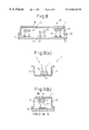
- FIG. 12 Such a known CSP is shown in FIG. 12, in which CPS 2 includes a semiconductor chip 10 having one surface, i.e., an electrode forming surface, on which are formed electrode terminals and re-wiring pads 12 to which first ends of respective wires 14 are connected.
- Each of the wires 14 is flexible, since it has a bent portion at an intermediate position, or portion, thereof.
- the other, second end 16 of the wire 14 is to be connected to a terminal on a mounting board.
- FIG. 13 shows a semiconductor device module in which a plurality of CSPs 2 are mounted on the mounting board 18 .
- the semiconductor device module shown in FIG. 13 includes a plurality of CSPs 2 each of which is connected to a pad 20 , as a terminal, on the mounting board 18 via a wire 14 . Connection between the wire 14 and the pad 20 is conducted by means of a solder 22 .
- the bent portion of the wire 14 reduces the thermal stress exerted on both the semiconductor element 10 and the mounting board 18 , caused by the difference in thermal expansion coefficient therebetween.
- a space is kept between an electrode forming surface 10 a of the semiconductor element 10 , facing the mounting board 18 , and the mounting board 18 .
- Thermal conductivity of the semiconductor device module shown in FIG. 13 can be improved as compared with that of a semiconductor device module having only a space between the bottom of the recessed heat spreader 26 and the other surface 10 a of the semiconductor element 10 .
- the length of the wires for connecting the respective pads 20 of the mounting board 18 to the pads 12 of the semiconductor element 10 is variable among the respective CSPs 2 , 2 , 2 , . . . and among the same CSP 2 , since the respective wires have respective bent portions. Therefore, the positions of the other surfaces 10 b of the semiconductor elements 10 of the CSPs 2 mounted on the mounting board 18 are different for the respective CSPs 2 and, therefore, the thickness of the thermal conductive resin 28 filled on the other surfaces 10 b of the semiconductor element 10 is variable so that the level of the thermal conductivity is different for the respective CSPs 2 . Thus, a heat accumulated portion may be generated in the semiconductor device module shown in FIG. 13 and may cause error
- the wires 14 extend upwardly from the pads 12 of the semiconductor elements 10 . Therefore, during assembling process of the semiconductor device module, wires 14 of CSP 2 may interfere with the other wires 14 or other parts and may thus be damaged. The wires could be transferred together but handing of the wires would then be troublesome.
- An object of the present invention is to provide a semiconductor device module and a semiconductor device module part, capable of absorbing the thermal stress caused by the difference in respective thermal expansion coefficients of a semiconductor device and a mounting board on which a semiconductor device is mounted, capable of obtaining a uniform heat radiation from the respective semiconductor devices, and affording easy assembling and handling of the semiconductor devices.
- the inventors have made an arrangement in which, in order to improve heat radiation from the other surface of the semiconductor element 10 , a peripheral edges of recessed portion of a heat spreader 26 is first adhered to a surface of the mounting board 18 by means of an adhesive layer 24 and, then, a bottom of the recessed portion of the heat spreader 26 are arranged to face to the other surfaces of the semiconductor elements 10 which constitute respective CSPs 2 , 2 , 2 , . . . , as shown in FIG. 12 .
- the inventors filled a thermal conductive resin 28 containing fillers of non-organic material, such as alumina, silica or the others, into a region between the bottom of the recessed heat spreader 26 and the other surface of the semiconductor element 10 , to improve the thermal conductivity.
- a thermal conductive resin 28 containing fillers of non-organic material such as alumina, silica or the others
- an apparatus for a semiconductor device module comprising: a plurality of semiconductor devices, each comprising a semiconductor element having first and second surfaces, pads formed on the first surface on which electrode terminals are also formed and curved, flexible wires having first ends fixed to the pads; a mounting board on which the semiconductor devices are mounted in such a manner that the other, second ends of the wires are connected to terminals on the mounting board; a heat spreader having a recessed inner wall provided with a peripheral edge thereof which is adhered to or engaged with the mounting board in such a manner that the second surfaces of the semiconductor elements faces to a bottom surface of the recessed inner wall; and a thermal conductive resin layer disposed between the second surface of the semiconductor element and the bottom surface of the recessed inner wall of the heat spreader, the thermal conductive resin layer having a substantially constant thickness.
- the peripheral edge of the heat spreader is adhered to the mounting board by means of an elastic resin to absorb a difference in thermal expansion due to a difference in thermal expansion coefficient therebetween.
- An inside region of the recessed inner wall of the heat spreader is filled with sealing resin in such a manner that the first surface of the semiconductor element is covered with the sealing resin and the wire protrudes from a surface of the sealing resin.
- the thermal conductive resin layer is provided for the respective semiconductor element.
- the thermal conductive resin layer is a film made of thermal conductive resin.
- the thermal conductive resin layer is made of a resin containing therein fillers made of non-organic material, such as alumina, silica or the other, and/or fillers made of metallic material, such as aluminum, copper or the other.
- the wire is provided at an intermediate position thereof with a bent portion.
- an apparatus for a semiconductor device module comprising: a plurality of semiconductor devices, each comprising a semiconductor element having first and second surfaces, pads formed on the first surface on which electrode terminals are also formed and curved, flexible wires having one end fixed to the pads; a mounting board on which the semiconductor devices are mounted in such a manner that the other end of the wire is connected to terminals on the mounting board; a heat spreader having a recessed inner wall provided with a peripheral edge thereof which is adhered to or engaged with the mounting board in such a manner that the second surface of the semiconductor element faces to a bottom surface of the recessed wall; and a spring member having one end connected to the bottom surface of the recessed wall of the heat spreader and the other end connected to the second surface of the semiconductor element.
- the spring member having one end connected to the heat spreader and the other end connected to the second surface of the semiconductor element, is made of a part of the recessed wall of the heat spreader which is cut and drawn therefrom.
- Each of a plurality of the spring members has one ends connected to the bottom surface of the inner recessed wall of the heat spreader and the other end adhered to the second surface of the semiconductor element.
- the second surface of the semiconductor element is adhered to the other end of the spring member by means of an adhesive layer.
- an apparatus for a semiconductor device module comprising: a least one semiconductor device comprising a semiconductor element having first and second surfaces, pads formed on the first surface on which electrode terminals are also formed and curved, flexible wires having one ends fixed to the pads; a heat spreader having a recessed inner wall provided with a peripheral edge thereof which is to be adhered to or engaged with a mounting board; and a thermal conductive resin layer disposed between the second surface of the semiconductor element and the bottom surface of the recessed inner wall of the heat spreader.
- FIG. 1 is a cross-sectional view of an embodiment of a semiconductor device module according to the present invention
- FIGS. 2 ( a ) and 2 ( b ) show a process for fabricating the semiconductor device module shown in FIG. 1;
- FIGS. 3 ( a ) and 3 ( b ) show another process for fabricating the semiconductor device module, including a module part, according to the present invention
- FIGS. 4 to 6 are cross-sectional views of other embodiments of a semiconductor device module according to the present invention.
- FIGS. 7 and 8 show a process for fabricating the semiconductor device module shown in FIG. 6;
- FIGS. 9 ( a ) and 9 ( b ) are cross-sectional views of still another embodiment of a semiconductor device module part and a module using the module part;
- FIG. 10 is a cross-sectional view of still another embodiment of a semiconductor device module of this invention.
- FIG. 11 shows a wire which can be used in this invention
- FIG. 12 shows another embodiment of a wire which can be used in this invention.
- FIG. 13 is a cross-sectional view of a semiconductor device module known in the prior art.
- a semiconductor device module of this invention can be used as a memory module.
- An embodiment of such a memory module is shown in FIG. 1 which includes a plurality of semiconductor devices, i.e., a plurality of CSP's 2 , such as shown in FIG. 12 .
- the CSP 2 , 2 , 2 , . . . are mounted on a mounting board 18 mainly made of resin. That is to say, a semiconductor chip 10 constituting respective CSPs 2 has a first surface 10 a , i.e., an electrode forming surface, on which are formed electrode terminals and re-wiring pads 12 to which first ends 14 b of wires 14 are connected.
- Each of the wires 14 is flexible, since it has a bent portion 14 a at an intermediate position, or portion, thereof.
- the other, second end 14 c of the wire 14 is connected to a pad 20 on the mounting board 18 .
- a connection between the other, second end of the wire 14 and the pad 20 of the mounting board 18 is provided by solder 22 .
- the heat spreader 26 has a peripheral edge 26 b which is adhered to a surface of the mounting board 18 by means of adhesive layer 30 and defines therewith a recessed inner portion 32 .
- a bottom interior surface 26 a of the recessed inner portion 32 faces the respective other surfaces of the semiconductor elements 10 .
- the adhesive layer 30 is preferably a low elastic resin, the elasticity coefficient of Young's modulus thereof being lower than 100 MPa at room temperature, to make it possible to absorb the difference in the thermal conductivity due to the difference of the thermal expansion coefficient between the heat spreader 26 made of metal and the mounting board 18 mainly made of resin.
- a low elastic resin may be a silicone or fluororesin rubber, polyorephyne elastomer, epoxy resin dispersed with rubber such as NBR, or others.
- Thermal conductive resin layers 34 , 34 , 34 , . . . made of thermal conductive resin are formed between the bottom interior surface 26 a of the heat spreader 26 surrounding the recessed inner portion 32 and the other, second surfaces 10 b of the semiconductor elements 10 .
- heat generated in the semiconductor elements 10 is transmitted through the thermal conductive resin layers 34 to the heat spreader 26 and, therefore, the thermal conductivity can be improved as compared with a semiconductor device module having no such thermal conductive resin layers 34 .
- the respective thermal conductive resin layers 34 , 34 , 34 , . . . have a same (i.e., common) thickness and, therefore, the amount of heat radiated from the respective semiconductor elements to the heat spreader 26 can thus be a uniform value. Thus, any heat accumulated portion would not be formed within the semiconductor device module and thus a heat radiation efficiency can be improved.
- the thermal conductive resin which forms the thermal conductive resin layers 34 may be a resin containing fillers of non-organic material, such as alumina, silica or other such materials, and/or metal fillers, such as aluminum, copper or other such metal fillers.
- the respective thicknesses of the thermal conductive resin layers 34 , 34 , 34 , . . . may be variable as far as the amount of heat radiated from the respective semiconductor elements 10 to the heat spreader 26 can be a uniform value.
- the semiconductor device module shown in FIG. 1 can be made by using a semiconductor device module part A as shown in FIG. 2 ( a ).
- the module part A includes the heat spreader 26 having a bottom interior surface 26 a to which the other, second surfaces 10 b of the semiconductor elements 10 are adhered by means of the thermal conductive resin layers 34 .
- the thermal conductive resin layers 34 for adhering the other surfaces of the semiconductor elements 10 to the bottom of the heat spreader 26 have substantially the same thickness, displacing the surfaces 10 b at a uniform spacing from the bottom interior surface 26 a and the wires 14 thus extending from the surfaces 10 a by respective distances which vary randomly, as seen in FIGS. 2 ( a ) and 2 ( b ). Therefore, in the module part A, the lengths of the respective wires 14 are different with respect to each other. Each wire 14 is provided at an intermediate portion thereof with a bent portion 14 a . Therefore, it is very difficult to make the height of the wires 14 uniform.
- each wire 14 has a bent portion 14 a at an intermediate portion thereof, the wire 14 can easily be bent and has an effective resilience. As shown in FIG. 2 ( b ), when the peripheral edge 26 a , surrounding the recess 32 of the heat spreader 26 , is adhered to the mounting board 18 by means of an adhesive layer 30 , the other, free ends 14 c of the respective wires 14 can be connected to the pads 20 on the mounting board 18 .
- a wire 14 which is higher than the other wires can be pushed between, the respective surface 10 a of each semiconductor element 10 and the mounting board 18 while the bent portion 14 a thereof resiliently deforms to regulate the effective length of that wire, until the other free ends 14 c of the wires 14 are brought into contact with the respective pads 20 on the mounting board 18 .
- the semiconductor device module part A shown in FIG. 2 ( a ) almost all of the CSPs 2 which are adhered to the bottom interior surface 26 a of the spreader 26 are accommodated in the inside of the recess 32 . Therefore, when the semiconductor device module part A is transported or stored in its state, the wires 14 may not interfere with wires of the other CSP 2 or the other parts, as compared with a CSP 2 which is transported or stored in its own free state. Therefore, the semiconductor device module can easily be made and the cost of production thereof can be reduced.
- the semiconductor elements 10 are exposed, each thereof together with its electrode forming surfaces 10 a .
- a sealing resin 36 is filled by a potting or other process within the recess 32 of the heat spreader 26 so as to completely cover the semiconductor elements 10 mounted on the bottom interior surface 26 a of the recess 32 of the heat spreader 26 to hermetically seal these semiconductor elements 10 .
- the bent portions 14 a of the wires 14 are protruded from an upper surface of the sealing resin 36 . If the bent portions 14 a of the wires 14 were sealed in the sealing resin 36 , it would become difficult to regulate the height of the respective wires 14 when the semiconductor device module part A is mounted on the mounting board 18 as shown in FIG. 3 ( b ).
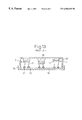
- the other, free ends 14 c of the wires 14 of the CSP 2 , 2 , 2 , . . . are fixed to the pads 20 of the mounting board 18 by means of solder 22 .
- solder 22 may not necessarily be used as shown in FIG. 4 .
- the wire 14 has a resilient property due to its bent portion 14 a , so that the other, free end 14 c of the wire 14 is always pushed toward the pad 20 on the mounting board 18 , owing to the resilient property of the wire itself.
- the heat spreader 26 can be, pushed toward mounting board 18 by a pushing member 37 which is hooked to the mounting board 18 by its jaws (or hooks) 37 a , 37 b extending beyond the peripheral edge 26 b of the heat spreader 26 , so that the peripheral edge 26 b of the heat spreader 26 is kept in contact with the surface of the mounting board 18 , without any adhesive layer between the peripheral edge 16 b of the heat spreader 26 and the mounting board 18 . Therefore, the mounting board 18 can easily be separated from the heat spreader 26 and the CSPs 2 , 2 , 2 , . . . by disengaging the hooks 37 b of the pushing member 37 from the mounting board 18 and therefore unacceptable CSPs 2 or the other unfavorable parts can easily be changed.
- peripheral sidewalls, surrounding recessed portion 32 , of the heat spreader 26 be provided with jaws (or hooks) to be engaged with the mounting board 18 so that the heat spreader 26 can be engaged with the mounting board 18 .
- the respective CSPs 2 , 2 , 2 , . . . and the recessed bottom interior surface 26 a of the heat spreader 26 are adhered to each other by means of respective thermal conductive resin layers 34 formed for the respective CSPs 2 .
- a continuous film 35 of thermal conductive resin alternatively can be used to cover the whole area of the recessed bottom interior surface 26 a of the heat spreader 26 .
- semiconductor device module part A having the thermal conductive resin layer 35 as shown in FIG.
- a double-sided adhesive film made of thermal conductive resin such as the thermal conductive resin layer 35 can be used to adhere, by one side thereof, to the recessed bottom interior surface 26 a of the heat spreader 26 and by the other side thereof to the respective CSP 2 , 2 , 2 , . . . .
- a one-sided adhesive film made of thermal conductive resin can be used to adhere by its adhesive side to the recessed bottom interior surface 26 a of the heat spreader 26 to form a thermal conductive resin layer 35 .
- the surface of the thermal conductive resin layer 35 facing to the CSP 2 is not adhesive. Therefore, CSP 2 , 2 , 2 , . . . are first mounted on the mounting board 18 . Such a mounting is conducted by fixing the other ends 14 c of the wires of respective CSP 2 , 2 , 2 , . . . to the respective pads 20 of the mounting board 18 by means of solder 22 . Then, the peripheral edge 26 b of the heat spreader 26 is adhered to the surface of the mounting surface by means of adhesive layer 30 .
- the surface of the thermal conductive resin layer 35 adhered to the recessed bottom of the heat spreader 26 pushes the other surfaces 10 b of the semiconductor elements 10 constituting the CSPs 2 , 2 , 2 , . . . Due to the pushing by the surface of the thermal conductive resin layer 35 , the bent portion of the wire of the CSP 2 , the other surface 10 b of the semiconductor element 10 being higher than that of the other CSP 2 , will be bent largely and the position of the other surface 10 b of the semiconductor element 10 becomes gradually lower. Finally, the other surface 10 b of the lowermost semiconductor element 10 comes into contact with the surface of the thermal conductive resin layer 35 and thus a semiconductor device module as shown in FIG. 8 can be obtained.
- a double-sided adhesive film made of thermal conductive resin can also be used, so that the surface of the thermal conductive resin layer 35 thus formed is adhesive.
- a plurality of CSPs 2 are mounted on the bottom of the recessed portion of the heat spreader 26 .
- a semiconductor device module part C as shown in FIG. 9 ( a )
- only one CSP 2 can be mounted on the bottom of the recessed portion of the heat spreader 26 by means of a thermal conductive resin layer 34 .
- this semiconductor device module part C almost all of the CSP 2 is accommodated in the inside of the recess 32 . Therefore, when the semiconductor device module part C is transported or stored in its state, the wires 14 may not interfere with the wires of the other CSP 2 or the other parts, as compared with a CSP 2 which is transported or stored in its own state. Therefore, the semiconductor device module of the invention can easily be made and the cost of production thereof can be reduced.
- FIG. 9 ( b ) shows a semiconductor device module obtained by using a semiconductor device module part C shown in FIG. 9 ( a ).
- the peripheral edge 26 b of the heat spreader 26 is adhered to the mounting board 18 by means of adhesive layer 30 and the other end 14 c of the lead wire 14 of CSP 2 is fixed to the pad 20 on the mounting board 18 by means of solder 22 .
- FIG. 10 shows another embodiment of a semiconductor device module.
- the peripheral edge 26 b of the heat spreader 26 is adhered to the surface of the mounting board 18 by means of an adhesive layer 30 and a spring member 38 having a first end connected to and extending integrally from the bottom wall heat spreader 26 surrounding the recess 32 is provided for the respective CSP 2 .
- the second end portion 40 of the spring member 38 is connected to the other surface of the semiconductor element 10 constituting the CSP 2 by means of thermal conductive resin layer 34 .
- the spring member 38 is formed by cutting and bending a part of the recessed bottom wall of the heat spreader 26 and has a lower resilience than that of the wire 14 of CSP 2 mounted on the mounting board 18 .
- the other end of the spring member 38 should be adjusted so as to be in contact with the other surface 10 b of the semiconductor element 10 which is located at the lowest position among the plurality of CSPs 2 , 2 , 2 , . . . mounted on the mounting board 18 .
- the heat spreader 26 in which the other ends of the spring members 38 are adjusted, is mounted on the mounting board 18 .
- the difference in height of the semiconductor elements 10 of the respective CSPs 2 , 2 , 2 , . . . can be absorbed by the spring member 38 which is brought into contact with the other surface 10 b of the semiconductor element 10 by means of thermal conductive resin layer 34 .
- heat generated in the semiconductor element 10 can be transmitted through the spring member 38 to the heat spreader 26 . Since the spring member 38 is made of the same material as that of the heat spreader 26 , the thermal conductivity thereof is better than that of the thermal conductive resin 28 used in the semiconductor device module shown in FIG. 13 . Thus, in this embodiment, the heat radiation efficiency is improved and the amount of heat radiation is more uniform than those in the semiconductor device module shown in FIG. 13 .
- the wire 14 which can be used in the CSP 2 may be a helical wire such as shown in FIG. 11 in place of a hair pin-shaped wire including two bent portions as shown in FIG. 12 .
- wiring on the one surface of the semiconductor element 10 is provided with a pad 12 to which one end of the wire 14 is connected.
- the wire 14 can be directly connected to the electrode terminal of the semiconductor.element 10 .
Abstract
Description
Claims (14)
Priority Applications (1)
| Application Number | Priority Date | Filing Date | Title |
|---|---|---|---|
| US09/422,850 US6586845B1 (en) | 1998-10-28 | 1999-10-25 | Semiconductor device module and a part thereof |
Applications Claiming Priority (2)
| Application Number | Priority Date | Filing Date | Title |
|---|---|---|---|
| JP30735298A JP3660814B2 (en) | 1998-10-28 | 1998-10-28 | Semiconductor module manufacturing method and semiconductor device module component manufacturing method |
| US09/422,850 US6586845B1 (en) | 1998-10-28 | 1999-10-25 | Semiconductor device module and a part thereof |
Publications (1)
| Publication Number | Publication Date |
|---|---|
| US6586845B1 true US6586845B1 (en) | 2003-07-01 |
Family
ID=28043574
Family Applications (1)
| Application Number | Title | Priority Date | Filing Date |
|---|---|---|---|
| US09/422,850 Expired - Fee Related US6586845B1 (en) | 1998-10-28 | 1999-10-25 | Semiconductor device module and a part thereof |
Country Status (1)
| Country | Link |
|---|---|
| US (1) | US6586845B1 (en) |
Cited By (12)
| Publication number | Priority date | Publication date | Assignee | Title |
|---|---|---|---|---|
| US20020187590A1 (en) * | 2000-08-31 | 2002-12-12 | Micron Technology, Inc. | Ball grid array packages with thermally conductive containers |
| US20030106924A1 (en) * | 2001-01-17 | 2003-06-12 | Kazuhiro Nobori | Electronic circuit device and method for manufacturing the same |
| US20060219284A1 (en) * | 2005-03-30 | 2006-10-05 | Yamaha Corporation | Thermoelectric conversion unit |
| US20070080337A1 (en) * | 2005-09-29 | 2007-04-12 | Osram Opto Semiconductors Gmbh | Radiation emitting component |
| US20070176289A1 (en) * | 2001-07-31 | 2007-08-02 | Chippac, Inc | Plastic Ball Grid Array Package with Integral Heatsink |
| US20070285884A1 (en) * | 2004-07-29 | 2007-12-13 | Micron Technology, Inc. | Interposer with flexible solder pad elements |
| US20080224288A1 (en) * | 2005-03-30 | 2008-09-18 | Nxp B.V. | Portable Object Connectable Package |
| US20090303679A1 (en) * | 2008-06-06 | 2009-12-10 | Inventec Corporation | Memory module |
| US20110192027A1 (en) * | 2006-06-16 | 2011-08-11 | International Business Machines Corporation | Thermally conductive composite interface, cooled electronic assemblies employing the same, and methods of fabrication thereof |
| US20120175766A1 (en) * | 2009-01-22 | 2012-07-12 | International Business Machines Corporation | System and method of achieving mechanical and thermal stability in a multi-chip package |
| US8384228B1 (en) | 2009-04-29 | 2013-02-26 | Triquint Semiconductor, Inc. | Package including wires contacting lead frame edge |
| US11328977B2 (en) * | 2019-06-11 | 2022-05-10 | Cobham Colorado Springs Inc. | Flip chip assembly |
Citations (13)
| Publication number | Priority date | Publication date | Assignee | Title |
|---|---|---|---|---|
| JPS6477954A (en) | 1987-09-18 | 1989-03-23 | Fujitsu Ltd | Package for semiconductor element |
| EP0359928A2 (en) | 1988-09-21 | 1990-03-28 | International Business Machines Corporation | Integrated circuit package with cooling means |
| JPH0394438A (en) | 1989-09-06 | 1991-04-19 | Shinko Electric Ind Co Ltd | Semiconductor chip module |
| EP0528606A2 (en) | 1991-08-13 | 1993-02-24 | Parker-Hannifin Corporation | Thermally conductive interface materials |
| US5476211A (en) | 1993-11-16 | 1995-12-19 | Form Factor, Inc. | Method of manufacturing electrical contacts, using a sacrificial member |
| JPH0878584A (en) | 1994-09-06 | 1996-03-22 | Hitachi Ltd | Electronic package |
| US5572070A (en) | 1995-02-06 | 1996-11-05 | Rjr Polymers, Inc. | Integrated circuit packages with heat dissipation for high current load |
| JPH08306832A (en) | 1995-05-01 | 1996-11-22 | Mitsubishi Electric Corp | Cooling equipment |
| US6078500A (en) * | 1998-05-12 | 2000-06-20 | International Business Machines Inc. | Pluggable chip scale package |
| US6114763A (en) * | 1997-05-30 | 2000-09-05 | Tessera, Inc. | Semiconductor package with translator for connection to an external substrate |
| US6236109B1 (en) * | 1999-01-29 | 2001-05-22 | United Microelectronics Corp. | Multi-chip chip scale package |
| US6309915B1 (en) * | 1998-02-05 | 2001-10-30 | Tessera, Inc. | Semiconductor chip package with expander ring and method of making same |
| EP1310566A2 (en) | 2001-10-08 | 2003-05-14 | Medizinische Hochschule Hannover | Method for the identification of a recombinant nucleic acid |
-
1999
- 1999-10-25 US US09/422,850 patent/US6586845B1/en not_active Expired - Fee Related
Patent Citations (13)
| Publication number | Priority date | Publication date | Assignee | Title |
|---|---|---|---|---|
| JPS6477954A (en) | 1987-09-18 | 1989-03-23 | Fujitsu Ltd | Package for semiconductor element |
| EP0359928A2 (en) | 1988-09-21 | 1990-03-28 | International Business Machines Corporation | Integrated circuit package with cooling means |
| JPH0394438A (en) | 1989-09-06 | 1991-04-19 | Shinko Electric Ind Co Ltd | Semiconductor chip module |
| EP0528606A2 (en) | 1991-08-13 | 1993-02-24 | Parker-Hannifin Corporation | Thermally conductive interface materials |
| US5476211A (en) | 1993-11-16 | 1995-12-19 | Form Factor, Inc. | Method of manufacturing electrical contacts, using a sacrificial member |
| JPH0878584A (en) | 1994-09-06 | 1996-03-22 | Hitachi Ltd | Electronic package |
| US5572070A (en) | 1995-02-06 | 1996-11-05 | Rjr Polymers, Inc. | Integrated circuit packages with heat dissipation for high current load |
| JPH08306832A (en) | 1995-05-01 | 1996-11-22 | Mitsubishi Electric Corp | Cooling equipment |
| US6114763A (en) * | 1997-05-30 | 2000-09-05 | Tessera, Inc. | Semiconductor package with translator for connection to an external substrate |
| US6309915B1 (en) * | 1998-02-05 | 2001-10-30 | Tessera, Inc. | Semiconductor chip package with expander ring and method of making same |
| US6078500A (en) * | 1998-05-12 | 2000-06-20 | International Business Machines Inc. | Pluggable chip scale package |
| US6236109B1 (en) * | 1999-01-29 | 2001-05-22 | United Microelectronics Corp. | Multi-chip chip scale package |
| EP1310566A2 (en) | 2001-10-08 | 2003-05-14 | Medizinische Hochschule Hannover | Method for the identification of a recombinant nucleic acid |
Cited By (22)
| Publication number | Priority date | Publication date | Assignee | Title |
|---|---|---|---|---|
| US20020187590A1 (en) * | 2000-08-31 | 2002-12-12 | Micron Technology, Inc. | Ball grid array packages with thermally conductive containers |
| US7399657B2 (en) * | 2000-08-31 | 2008-07-15 | Micron Technology, Inc. | Ball grid array packages with thermally conductive containers |
| US20030106924A1 (en) * | 2001-01-17 | 2003-06-12 | Kazuhiro Nobori | Electronic circuit device and method for manufacturing the same |
| US20050148237A1 (en) * | 2001-01-17 | 2005-07-07 | Kazuhiro Nobori | Electronic circuit device |
| US6943443B2 (en) * | 2001-01-17 | 2005-09-13 | Matsushita Electric Industrial Co., Ltd. | Electronic circuit device including metallic member having installation members |
| US7208833B2 (en) | 2001-01-17 | 2007-04-24 | Matsushita Electric Industrial Co., Ltd. | Electronic circuit device having circuit board electrically connected to semiconductor element via metallic plate |
| US8030756B2 (en) * | 2001-07-31 | 2011-10-04 | Chippac, Inc. | Plastic ball grid array package with integral heatsink |
| US20070176289A1 (en) * | 2001-07-31 | 2007-08-02 | Chippac, Inc | Plastic Ball Grid Array Package with Integral Heatsink |
| US9412677B2 (en) | 2004-07-29 | 2016-08-09 | Micron Technology, Inc. | Computer systems having an interposer including a flexible material |
| US20070285884A1 (en) * | 2004-07-29 | 2007-12-13 | Micron Technology, Inc. | Interposer with flexible solder pad elements |
| US20080224288A1 (en) * | 2005-03-30 | 2008-09-18 | Nxp B.V. | Portable Object Connectable Package |
| US7692280B2 (en) * | 2005-03-30 | 2010-04-06 | St-Ericsson Sa | Portable object connectable package |
| US20060219284A1 (en) * | 2005-03-30 | 2006-10-05 | Yamaha Corporation | Thermoelectric conversion unit |
| US7675085B2 (en) * | 2005-09-29 | 2010-03-09 | Osram Opto Semiconductors Gmbh | Radiation emitting component |
| US20070080337A1 (en) * | 2005-09-29 | 2007-04-12 | Osram Opto Semiconductors Gmbh | Radiation emitting component |
| US20110192027A1 (en) * | 2006-06-16 | 2011-08-11 | International Business Machines Corporation | Thermally conductive composite interface, cooled electronic assemblies employing the same, and methods of fabrication thereof |
| US8322029B2 (en) * | 2006-06-16 | 2012-12-04 | International Business Machines Corporation | Thermally conductive composite interface, cooled electronic assemblies employing the same, and methods of fabrication thereof |
| US20090303679A1 (en) * | 2008-06-06 | 2009-12-10 | Inventec Corporation | Memory module |
| US20120175766A1 (en) * | 2009-01-22 | 2012-07-12 | International Business Machines Corporation | System and method of achieving mechanical and thermal stability in a multi-chip package |
| US8421217B2 (en) * | 2009-01-22 | 2013-04-16 | International Business Machines Corporation | Achieving mechanical and thermal stability in a multi-chip package |
| US8384228B1 (en) | 2009-04-29 | 2013-02-26 | Triquint Semiconductor, Inc. | Package including wires contacting lead frame edge |
| US11328977B2 (en) * | 2019-06-11 | 2022-05-10 | Cobham Colorado Springs Inc. | Flip chip assembly |
Similar Documents
| Publication | Publication Date | Title |
|---|---|---|
| US6586845B1 (en) | Semiconductor device module and a part thereof | |
| US5227663A (en) | Integral dam and heat sink for semiconductor device assembly | |
| KR101244075B1 (en) | Power surface mount light emitting die package | |
| US5777386A (en) | Semiconductor device and mount structure thereof | |
| US5175612A (en) | Heat sink for semiconductor device assembly | |
| KR101141492B1 (en) | Composite leadframe led package and method of making the same | |
| KR100709890B1 (en) | Light emitting diode package having multiple molding resins | |
| US20020175401A1 (en) | Semiconductor package with stacked chips | |
| US20060091512A1 (en) | Semiconductor device and manufacturing process thereof | |
| KR20010031110A (en) | Method and construction for thermally enhancing a microelectronic pakage | |
| JPH09153574A (en) | Semiconductor device and semiconductor module | |
| JP2007305761A (en) | Semiconductor device | |
| US6713865B2 (en) | Semiconductor device having semiconductor element housed in packed with heat sink | |
| EP0997937A2 (en) | Semiconductor device module with a heat sink | |
| JP4527462B2 (en) | Electronic components | |
| US20180204782A1 (en) | Semiconductor device and method of manufacturing the same | |
| JP4994025B2 (en) | Resin-sealed electronic equipment | |
| JPS634652A (en) | Semiconductor device | |
| CN216871951U (en) | Radiator mounting structure of flip chip | |
| JP4060020B2 (en) | Semiconductor device | |
| KR100191854B1 (en) | High thermal emissive semiconductor chip package having heat sink | |
| JP3159088B2 (en) | Radiation fin fastener for LSI package | |
| JPH0290555A (en) | Semiconductor device | |
| JP3110862B2 (en) | Semiconductor device | |
| JP2019204819A (en) | Electronic device |
Legal Events
| Date | Code | Title | Description |
|---|---|---|---|
| AS | Assignment |
Owner name: SHINKO ELECTRIC INDUSTRIES CO.,LTD., JAPAN Free format text: ASSIGNMENT OF ASSIGNORS INTEREST;ASSIGNORS:HIGASHI, MITSUTOSHI;KOIKE, NIROKO;REEL/FRAME:010352/0246 Effective date: 19991013 |
|
| AS | Assignment |
Owner name: SHINKO ELECTRIC INDUSTRIES CO., LTD., JAPAN Free format text: (ASSIGNMENT OF ASSIGNOR'S INTEREST) RECORD TO CORRECT THE SECOND INVENTOR'S NAME ON A DOCUMENT PREVIOUSLY RECORDED AT REEL/010352, FRAME/0246.;ASSIGNORS:HIGASHI, MITSUTOSHI;KOIKE, HIROKO;REEL/FRAME:010646/0310 Effective date: 19991013 |
|
| AS | Assignment |
Owner name: SHINKO ELECTRIC INDUSTRIES CO., LTD., JAPAN Free format text: CORRECTED RECORDATION FORM COVER SHEET REEL/FRAME 010646-0310.;ASSIGNORS:HIGASHI, MITSUTOSHI;KOIKE, HIROKO;REEL/FRAME:010880/0350 Effective date: 19991013 |
|
| CC | Certificate of correction | ||
| FEPP | Fee payment procedure |
Free format text: PAYER NUMBER DE-ASSIGNED (ORIGINAL EVENT CODE: RMPN); ENTITY STATUS OF PATENT OWNER: LARGE ENTITY Free format text: PAYOR NUMBER ASSIGNED (ORIGINAL EVENT CODE: ASPN); ENTITY STATUS OF PATENT OWNER: LARGE ENTITY |
|
| FPAY | Fee payment |
Year of fee payment: 4 |
|
| REMI | Maintenance fee reminder mailed | ||
| LAPS | Lapse for failure to pay maintenance fees | ||
| STCH | Information on status: patent discontinuation |
Free format text: PATENT EXPIRED DUE TO NONPAYMENT OF MAINTENANCE FEES UNDER 37 CFR 1.362 |
|
| FP | Lapsed due to failure to pay maintenance fee |
Effective date: 20110701 |