US6610991B1 - Electronics assembly apparatus with stereo vision linescan sensor - Google Patents
Electronics assembly apparatus with stereo vision linescan sensor Download PDFInfo
- Publication number
- US6610991B1 US6610991B1 US09/434,325 US43432599A US6610991B1 US 6610991 B1 US6610991 B1 US 6610991B1 US 43432599 A US43432599 A US 43432599A US 6610991 B1 US6610991 B1 US 6610991B1
- Authority
- US
- United States
- Prior art keywords
- detector
- feature
- component
- optical
- image
- Prior art date
- Legal status (The legal status is an assumption and is not a legal conclusion. Google has not performed a legal analysis and makes no representation as to the accuracy of the status listed.)
- Expired - Fee Related
Links
Images


Classifications
-
- G—PHYSICS
- G01—MEASURING; TESTING
- G01B—MEASURING LENGTH, THICKNESS OR SIMILAR LINEAR DIMENSIONS; MEASURING ANGLES; MEASURING AREAS; MEASURING IRREGULARITIES OF SURFACES OR CONTOURS
- G01B11/00—Measuring arrangements characterised by the use of optical techniques
- G01B11/02—Measuring arrangements characterised by the use of optical techniques for measuring length, width or thickness
- G01B11/024—Measuring arrangements characterised by the use of optical techniques for measuring length, width or thickness by means of diode-array scanning
-
- H—ELECTRICITY
- H05—ELECTRIC TECHNIQUES NOT OTHERWISE PROVIDED FOR
- H05K—PRINTED CIRCUITS; CASINGS OR CONSTRUCTIONAL DETAILS OF ELECTRIC APPARATUS; MANUFACTURE OF ASSEMBLAGES OF ELECTRICAL COMPONENTS
- H05K13/00—Apparatus or processes specially adapted for manufacturing or adjusting assemblages of electric components
- H05K13/08—Monitoring manufacture of assemblages
- H05K13/081—Integration of optical monitoring devices in assembly lines; Processes using optical monitoring devices specially adapted for controlling devices or machines in assembly lines
- H05K13/0812—Integration of optical monitoring devices in assembly lines; Processes using optical monitoring devices specially adapted for controlling devices or machines in assembly lines the monitoring devices being integrated in the mounting machine, e.g. for monitoring components, leads, component placement
-
- H—ELECTRICITY
- H01—ELECTRIC ELEMENTS
- H01L—SEMICONDUCTOR DEVICES NOT COVERED BY CLASS H10
- H01L2224/00—Indexing scheme for arrangements for connecting or disconnecting semiconductor or solid-state bodies and methods related thereto as covered by H01L24/00
- H01L2224/74—Apparatus for manufacturing arrangements for connecting or disconnecting semiconductor or solid-state bodies and for methods related thereto
- H01L2224/78—Apparatus for connecting with wire connectors
-
- H—ELECTRICITY
- H01—ELECTRIC ELEMENTS
- H01L—SEMICONDUCTOR DEVICES NOT COVERED BY CLASS H10
- H01L24/00—Arrangements for connecting or disconnecting semiconductor or solid-state bodies; Methods or apparatus related thereto
- H01L24/74—Apparatus for manufacturing arrangements for connecting or disconnecting semiconductor or solid-state bodies
- H01L24/78—Apparatus for connecting with wire connectors
-
- H—ELECTRICITY
- H01—ELECTRIC ELEMENTS
- H01L—SEMICONDUCTOR DEVICES NOT COVERED BY CLASS H10
- H01L2924/00—Indexing scheme for arrangements or methods for connecting or disconnecting semiconductor or solid-state bodies as covered by H01L24/00
- H01L2924/0001—Technical content checked by a classifier
- H01L2924/00014—Technical content checked by a classifier the subject-matter covered by the group, the symbol of which is combined with the symbol of this group, being disclosed without further technical details
-
- H—ELECTRICITY
- H01—ELECTRIC ELEMENTS
- H01L—SEMICONDUCTOR DEVICES NOT COVERED BY CLASS H10
- H01L2924/00—Indexing scheme for arrangements or methods for connecting or disconnecting semiconductor or solid-state bodies as covered by H01L24/00
- H01L2924/10—Details of semiconductor or other solid state devices to be connected
- H01L2924/11—Device type
- H01L2924/12—Passive devices, e.g. 2 terminal devices
- H01L2924/1204—Optical Diode
- H01L2924/12041—LED
-
- H—ELECTRICITY
- H01—ELECTRIC ELEMENTS
- H01L—SEMICONDUCTOR DEVICES NOT COVERED BY CLASS H10
- H01L2924/00—Indexing scheme for arrangements or methods for connecting or disconnecting semiconductor or solid-state bodies as covered by H01L24/00
- H01L2924/10—Details of semiconductor or other solid state devices to be connected
- H01L2924/11—Device type
- H01L2924/14—Integrated circuits
Definitions
- the present invention relates to imaging systems for electronic components, such as those used in pick and place machines, and more particularly to imaging systems which image a portion of a component onto a linear detector line by line, and are able to provide information about the height of a feature on the component.
- Prior art systems for detecting height and coplanarity can be divided into two separate groups; those which are based on a linear detector and those which are not (e.g., vision based and large array detectors systems).
- Vision based and large array detector systems are typically not “on-head” systems.
- a sensor senses the orientation and condition (e.g., coplanar, absence/presence of features, etc.) of the component while the component is transported to the printed circuit board.
- On-head systems are preferred over other systems because they provide exceptional efficiency in placing the component, leading to a high throughput in the electronic assembly operation.
- off-head systems have a sensor which senses the orientation and condition of a component with a fixed inspection system.
- Vision based and large array detector systems have a fairly large weight and size, so as to limit the scanning speed for the sensor in an “on-head” application.
- Linescan sensor systems are characterized by having a linear detector and are adapted to scan a portion of a component.
- Associated electronics assemble multiple scans of a portion of a component and provide a composite image of the area of interest on a component.
- existing linescan systems are typically off-head which slows down the process of placing the component.
- many are based on the principle of triangulation (the use of structured light to compute a height), which requires complex optics and registration in the sensor.
- the prior art lacks a versatile, compact linescan sensor system reporting coplanarity, component quality and orientation of the object, which system is adapted for use either in “on-head” or “off-head” applications.
- the ideal system would allow for inspection of features on different types of complex components at high throughput, and be easily adapted for use with pick and place machines, wire bonders and screen printers.
- An imaging system which provides orientation information as well as height information about the object.
- the imaging system includes a linescan sensor, which views the object from at least two views and outputs a set of partial images of the object for each view. Once the at least two sets of partial images are combined into an assembled image, electronics compute the height of object features from the at least two assembled images.
- the height information is particularly useful to assess the quality of a feature on an electronic component, such as a ball, grid, lead, or column.
- Orientation information about the object can be computed from one or more of the assembled images. Once the height of at least four features on the object is computed, a measure of the coplanarity of the component may be computed. Additionally, the height information from the present invention may be used to assess the quality of an object, such as ascertaining the absence or presence of critical features on the object.
- the method and apparatus of the present invention is useful for both single and multi-nozzle pick and place machines, but may also be used with screen printers to assess whether applied solder bricks are present or absent, or to assess whether the height of the solder bricks is appropriate.
- the method and apparatus of the present invention is useful with wire bonders, to ascertain the height of a bonded wire or the like as a measure of the quality of the bonding process.
- FIG. 1 is a top plan view of a pick and place machine.
- FIG. 2 is an elevation view of a placement head in accordance with an embodiment of the present invention.
- FIG. 3 is a side elevation view of a portion of a placement head in accordance with an embodiment of the present invention.
- FIGS. 4-6 are rear elevation and two top plan views of a portion of a placement head in accordance with an embodiment of the present invention.
- FIG. 7 is a flowchart of a method of picking and placing components in accordance with an embodiment of the present invention.
- FIG. 8 is a timing diagram of component placement in accordance with an embodiment of the present invention.
- FIG. 9 is a diagrammatic view of a portion of a pick and place machine in accordance with an embodiment of the present invention.
- FIG. 10 is a system block diagram of a portion of a pick and place machine in accordance with an embodiment of the present invention.
- FIGS. 11 a and 11 b are perspective and side elevation views of a gradient index lens array imaging system.
- FIGS. 12 and 13 are diagrammatic views of a stereo imaging system.
- FIGS. 14 a and 14 b are diagrammatic views of a detector in the X-Y plane.
- FIG. 15 is a diagrammatic view of a telecentric imaging system.
- FIG. 16 is a diagrammatic view of a telecentric imaging system imaging multiple ray bundles.
- FIG. 17 is a diagrammatic view of another telecentric imaging system.
- FIG. 18 is a diagrammatic view of another optical system.
- FIG. 19 is a diagrammatic view of an optical system imaging multiple ray bundles.
- FIG. 20 is a diagrammatic view of an optical system including a prism.
- FIG. 21 is a diagrammatic Y-Z plane view of a portion of an optical system in accordance with an embodiment of the present invention.
- FIG. 22 is a diagrammatic X-Y plane view of a detector in accordance with an embodiment of the present invention.
- FIG. 23 is a diagrammatic view of a stereo vision optical system in accordance with an embodiment of the present invention.
- FIG. 24 is a diagrammatic X-Y plane view of the detector shown in FIG. 22, imaging a feature in accordance with an embodiment of the present invention.
- FIG. 25 is a diagrammatic view of a sensor in accordance with an embodiment of the present invention.
- FIG. 26 is a perspective view of a prior art wire bonder.
- FIG. 27 is a top plan view of a wire bonder in accordance with an embodiment of the present invention.
- the method and apparatus of the present invention is best understood by first disclosing a preferred linescan sensor for use with the present invention. After a complete discussion of the preferred embodiments of this preferred linescan sensor, the theory and embodiments of the present height sensing linescan sensor will be detailed. It is understood that the method of the present invention may be practiced with other types of linescan sensors or any sensor having a linear detector which builds up an image of an object line by line.
- FIG. 1 is a top plan view of pick and place machine 50 in accordance with an embodiment of the invention. Although much of the present invention will be described with respect to pick and place machine 50 , other forms of pick and place machines, such as a split gantry design, are useful with embodiments of the present invention. Additionally, although embodiments of the present invention will be described with respect to pick and place machines, some embodiments of the present invention include an imaging system provided with a wire bonder or screen printer, as will be described with respect to FIGS. 19 and 21. As shown in FIG. 1, machine 50 includes transport mechanism 52 that is adapted to transport a workpiece such as a printed circuit board. Transport mechanism 52 includes mounting section 54 and conveyor 56 .
- Transport mechanism 52 is disposed on base 58 such that a workpiece is carried to mounting section 54 by conveyor 56 .
- Component reservoirs 60 are disposed on either side of transport mechanism 52 and supply electronic components. Reservoirs 60 can be any suitable device adapted to provide electronic components, such as a tape feeder.
- Pick and place machine 50 includes head 62 disposed above base 58 .
- Head 62 is movable between either of component reservoirs 60 and mounting section 54 .
- head supports 64 are movable on rails 66 thereby allowing head 62 to move in the Y direction over base 58 . Movement of head 62 in the Y direction occurs when motor 70 , in response to a motor actuation signal, rotates ball screw 72 which engages one of head supports 64 to thereby displace the support 64 is the Y direction.
- Head 62 is also supported upon rail 68 to allow head movement in the X direction relative to base 58 . Movement of head 62 in the X direction occurs when motor 74 , in response to a motor actuation signal, rotates ball screw 76 which engages head 62 and displaces head 62 in the X direction.
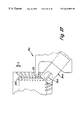
- head 62 includes body 78 , nozzle mount 80 , nozzles 82 and sensor 84 .
- Nozzle mount 80 is disposed within body 78 and mounts each of nozzles 82 within body 78 .
- Each of nozzles 82 is movable in the Z direction (up/down) and is rotatable about the Z axis by suitable actuation members, such as servo motors.
- Sensor 84 is adapted to move in the X direction relative to nozzles 82 to acquire images of components held by nozzles 82 .
- Sensor 84 is coupled to image processor 86 .
- Image processor 86 receives video data from sensor 84 based upon images of components held by nozzles 82 .
- Image processor 86 is adapted through hardware, software, or a combination of both, to calculate respective component orientations of each of the components held by the respective nozzles 82 . Image processor 86 then sends suitable orientation information to a controller (not shown) such that each of nozzles 82 is successively displaced to properly mount its respective component upon the workpiece.
- a controller not shown
- pick and place machine 50 can include a singular nozzle to practice embodiments of the present invention.
- FIG. 2 is an elevation view of head 62 in accordance with one embodiment of the present invention.
- Head 62 includes motor 88 operably coupled to a ball screw (not shown) through belt 89 .
- the ball screw is operably coupled to sensor 84 such that energization of motor 88 causes sensor 84 to move in the X axis direction relative to nozzles 82 .
- Sensor 84 can be adapted to image components coupled to nozzles 82 while scanning in either X axis direction. When such bi-directional scanning is employed, it is useful to provide image processing software that corrects for the fact that the data from scans of opposite directions are essentially flipped around from one another. Additionally, in some bi-directional scanning embodiments, sensor 84 can store the various scanned lines in temporary memory and then send them to the image processing section in correct order.
- FIG. 3 is an elevation view of head 87 in accordance with an embodiment of the invention.
- Head 87 includes plate 90 to which nozzles 82 and linear stage 92 are mounted.
- Sensor 84 is coupled to linear stage 92 via bracket 94 such that sensor 84 is moveable relative to nozzles 82 and thus component 96 .
- sensor 84 is moveable in the X axis direction relative to components 96 .
- FIG. 5 is a top plan view of head 87 in accordance with an embodiment of the present invention. For clarity, only four nozzles 82 are shown in FIG. 5 . However, any appropriate number of nozzles, including one nozzle, can be used.
- head 87 is movable in X and Y axis directions, respectively.
- sensor 84 is movable in the X axis direction with respect to nozzles 82 via its coupling to linear stage 92 .
- Sensor 84 includes detector window 102 which allows a line of sight between a linear detector (not shown) disposed within sensor 84 and a portion of a component held by one of nozzles 82 .
- the line of sight is preferably parallel to the axis of nozzles 82 .
- Each of nozzles 82 within the pick and place machine can be adapted to pick and place a different type of electrical component. Examples of such different component types include flip-chips, ball grid arrays (BGA's), micro ball grid arrays, quad flat pack (QFP), connector, pin grid array, dual inline package, single inline package, plastic leaded chip carrier (PLCC), chip capacitors, and chip resistors.
- each nozzle 82 can be independently adapted to pick and place a different type of component than other nozzles 82 . Because different component types can require different image resolutions, embodiments of the present invention can preferably change image resolution based upon component type.
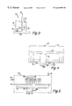
- FIG. 6 is a top plan view of placement head 104 for a pick and place machine in accordance with another embodiment of the present invention.
- Head 104 bears many similarities to head 87 , and like components are numbered similarly.
- head 104 includes body 7 and one or more nozzles 82 .
- Sensor 106 is moveable relative to nozzles 82 since sensor 106 is coupled to motor 88 via ball screw 108 .
- Motor 88 also includes encoder 110 that provides a feedback signal indicative of rotational displacement of ball screw 108 and thus axial displacement of sensor 106 in the X direction.
- sensor 106 includes a detector window 112 that is perpendicular to a longitudinal axis 114 of sensor 106 .
- Detector window 112 can be positioned anywhere on sensor 106 . Thus, if sensor 106 is adapted to scan components in a single direction (for example while moving to the right) then window 112 can be disposed proximate a leading edge 111 of sensor 106 such that components are scanned more quickly. In embodiments where sensor 106 is adapted to scan components in either direction (left and right) window 112 is preferably centered upon sensor 106 .
- FIG. 7 is a flowchart of a method of picking and placing n components upon a workpiece in accordance with the present invention.
- sequential operations for practicing the method of the present invention are disclosed. It is understood that for any successive sequential operations, that the first operation need only be commenced before the second operation is started.
- n components are picked up by a pick and place machine head, such as head 87 .
- blocks 122 and 124 are initiated.
- a linescan camera begins moving relative to the components as indicated by block 122 and the head begins traveling to the approximate position or site on the workpiece where the first component will be mounted.
- blocks 122 and 124 are executed substantially simultaneously.
- a counter is initialized to equal 1 .
- Counter P is used to track which component coordinates are being computed, as will be described in greater detail with respect to the rest of FIG. 7 .
- blocks 126 , 128 , and 132 preferably begin execution.
- blocks 122 , 126 , 128 and 130 execute while the head is transporting components to the approximate placement site.
- the linescan camera passes all n components and collects video data based upon the components.
- the video data is corrected for non-uniformities. Such non-uniformities may be due to changes in sensor scan speed that occur while scanning is performed.
- X, Y and ⁇ offset adjustments for component c p are computed.
- Height information is computed in accordance with embodiments of the invention set forth later in the specification. The height information is useful for assessing the location of pins, columns or leads (as appropriate for the component in view), the absence or presence of certain features on the component, such as balls, pins, columns or grids, the distance between leads if the component under test is leaded, or a computation of coplanarity. Once the height of a feature is computed, the coplanarity of that feature with respect to a reference plane may be computed.
- a reference plane is selected which is formed by at least three of the features (typically balls, columns or pins) and the deviation of any particular feature from the plane is computed and reported, although in many instances the deviation, computed as an average, standard deviation or the like, is compared to a threshold value to determine whether the component should be discarded or placed.
- the computed offset adjustments are used in block 134 to calculate final part placement coordinate endpoints for component c p .
- counter P is incremented as indicated in block 136 .
- the machine checks to determine whether the incremented counter (P) exceeds the number of components (n) picked up in block 120 , as indicated at block 138 . If the incremented counter exceeds the number of components, then control passes to block 140 and offset calculations cease. However, if the incremented counter does not exceed the number of components, control returns to block 132 and offset adjustments for component cp are computed.
- the loop continues with block 132 providing computed offset adjustments to block 134 until offset adjustments have been computed for all n components.
- part c p is placed as indicated at block 137 .
- the machine checks to determine whether c p is the last component. If component c p is not the last component, control returns to block 124 and the head begins moving to the approximate placement site of the next component. However, if all n components have been placed, then control returns to block 120 and an additional n components are picked up and the method repeats. Preferably, the various steps of placing parts occur while component offset adjustments are calculated.
- FIG. 8 is an example scan timing chart for a pick and place machine having four nozzles in accordance with an embodiment of the present invention.
- the vertical lines in FIG. 8 indicate specific time intervals.
- nozzle scanning requires three time intervals for completion.
- nozzle scanning which begins at time to will finish at time t 3 .
- nozzle # 1 is scanned, partial images of the component held by nozzle # 1 begin to be transferred at time t 1 .
- t 2 while the nozzle is still being scanned, and while the image is still being transferred, video processing begins.
- FIG. 9 is a diagrammatic view of sensor 106 , which is adapted to generate a two-dimensional image of component 96 as sensor 106 scans a portion of component 96 .
- Sensor 106 is operably coupled to motor 88 via ballscrew 108 .
- Motor 88 is operably coupled to encoder 110 which provides an indication of rotary displacement of ballscrew 108 and thus axial displacement of sensor 106 along the X axis.
- a linear glass scale type encoder could be substituted for encoder 110 .
- Linear detector 150 is preferably a charge coupled device (CCD) comprising a number of photoelements (pixels) arranged in a line. Preferably, the size of each pixel is approximately 14 microns square.
- Detector 150 is preferably manufactured by Dalsa Inc., of Waterloo Ontario and is model no. IL-CC-2048, although other types of linear detectors may be used in the present invention.
- Linear detector 150 is optically coupled to a portion of leads 154 through imaging optics 156 and detector window 158 . Imaging optics 156 can include lens system 160 and partial mirror 162 .
- sensor 106 also includes one or more illuminators.
- the embodiment shown in FIG. 9 includes darkfield illuminators 164 , diffuse illuminators 166 , brightfield illuminator 168 , and backlight illuminator 169 .
- darkfield illumination is intended to mean illumination which impinges upon the component at a high angle of incidence.
- Diffuse illumination is intended to mean illumination impinging upon the component at a lesser degree of incidence.
- Brightfield illumination is intended to mean illumination which impinges upon the component at a substantially zero incidence angle.
- brightfield illumination can also be considered specular or through-the-lens illumination.
- Backlight illumination as the term is used herein, is intended to mean illumination which originates from a position behind the component with respect to the sensor.
- the combination of these four types of illuminators is helpful to provide enhanced inspection capabilities with the sensors of the present invention, since the illumination types and their various combinations allow features to be identified with greater resolution.
- sensor 106 In operation, sensor 106 is moved along the X-axis with respect to component 96 . While in motion, sensor 106 acquires individual linear images, or partial images, of portions of component 96 . By storing multiple linear images and correlating the individual images with sensor location information provided by encoder 110 , an image of component 96 can be constructed.
- Illumination emanating from any of darkfield illuminators 164 , diffuse illuminators 166 or brightfield illuminator 168 is reflected by a portion of component 96 proximate detector window 158 . Additionally, backlight illumination from illuminator 169 can be used, where illumination emanates from source 171 and passes through diffuser 173 to backlight the component. The reflected illumination is redirected by partial mirror 156 through lens system 160 , and thereby focused upon linear detector 150 . Each individual pixel of linear detector 150 provides a representation of the sum of illumination incident on the pixel during an integration period.
- Lens system 160 can be any suitable optical device capable of focusing an object line upon linear detector 150 .
- lens system 160 can be a refractive lens system or a diffractive lens system.
- a refractive lens system can preferably include a gradient index (GRIN) lens array, available from NSG America, Inc., of Somerset N.J., or a traditional refractive lens system.
- a diffractive lens system can include a holographic lens array.
- Sensor 106 is coupled to sensor controller 170 of host 172 .
- Sensor controller 170 can receive and store each individual image line in a frame buffer, and provide suitable signals to sensor 106 to control the intensity of any of illuminators 164 , 166 , 168 , and 169 . Since host 172 is coupled to encoder 110 , sensor controller 170 can provide illumination intensity signals to any of the illuminators based upon position of sensor 106 along the X-axis or based upon the scan speed of sensor 106 along the X-axis.
- Host 172 also includes motion controller 174 that is coupled to motor 88 , nozzle motor 176 and a nozzle encoder (not shown).
- host 172 acquires an image of component 96 from linear detector 150 as sensor 106 is moved in the X direction relative to component 96 .
- Host 172 is adapted through suitable software, hardware, or both, to compute a current orientation of component 96 in X-axis, Y-axis, and ⁇ directions. Based upon the computed orientation, host 172 causes motion controller 174 to issue suitable motion commands to motors 70 , 74 (shown in FIG. 1) and nozzle motor 176 to cause nozzle 82 to deposit component 96 in a desired component position and orientation on the workpiece.
- Motion controller 174 is adapted to vary scan speed.
- FIG. 10 is a system block diagram of one embodiment of the height sensing sensor of the present invention and shows sensor head 700 mechanically coupled to a sensor motion system 702 , which provides uniaxial motor drive for head 700 .
- the system is “on-head”, since sensor head 700 moves with component head 708 .
- sensor head 700 , sensor motion system 702 , host 706 and component head 708 form a closed control loop 709 (not shown).
- host processor 712 sends a desired placement signal to the component head motor drive 724 .
- System 724 starts to move the component head 708 to the nominal placement location.
- the combination of sensor head 700 and sensor motor system 702 scan the component to provide partial images of the component during the scan
- the video formatter 714 assembles a plurality of partial images to form 1, 2, 3, or more assembled images of the component
- video processor 714 processes the assembled images to compute an x, y, and ⁇ orientation of the component, the height of certain features and optionally the coplanarity. Height computation uses any two of the assembled images. Computation of X, Y, ⁇ can use a single normal incidence assembled image. Additionally, X, Y, ⁇ can also be computed from two “angled” assembled images.
- Video processor 728 sends the orientation information to host processor 712 in pick and place machine 706 , which computes a correction signal as a function of a desired orientation and the present orientation.
- the correction signal is provided to the placement head 708 to properly orient and place the component.
- a host processor 712 within pick and place machine 706 , sends a desired placement location to component head 708 via bus 720 and bus 710 .
- Video formatter 714 receives outputs from detector read-out block 716 in sensor head 700 , via bus 718 .
- the function of formatter 714 is preferably carried out in a separate electronic chip than processor 712 , but if a minimum of functionality is desired, they may be embodied in the same component.
- Formatter 714 collects partial images that it receives, and assembles the partial images into first and second, and optionally third assembled images.
- formatter 714 optionally performs windowing of specific areas of the assembled images, (e.g., corners), performs magnification of specific areas and also may provide non-uniformity correction of the assembled images, where one of the dimensions of the image is disproportionately modified with respect to other dimensions of the assembled image, due to non-uniform spacing of partial images in time or space.
- Internal bus 720 connects formatter 714 , processor 712 , operator interface and display 722 , placement head motion control system 724 and video processor 728 .
- processor 712 also provides various timing signals for proper operation of the pick and place machine 706 .
- host processor includes suitable collision avoidance functionality to prevent collisions between the various component heads and between the sensor and the nozzles.
- Operator interface and display 722 allows the operator of the pick and place machine to program specific movements and associated timing of scans, as well as overall operation and diagnostics of the pick and place machine. A video display of the assembled image is also displayed for the operator.
- Placement head motion control system 724 includes a set of x, y, z, and ⁇ motors for moving component head 708 in the x, y, z, and ⁇ directions, as well as control electronics 726 for timing such movements and re-formatting the electrical digital signals from host processor 712 into analog signals generally required to drive the x, y, z, and ⁇ motors.
- a bank of x, y, z, and ⁇ encoders encodes the position of component head 708 and provides these signals to host processor 712 .
- Video processor 728 can be a microprocessor such as an Intel Pentium® processor. It is preferably included in every embodiment of the present invention, since it provides the basic x, y, and ⁇ location information necessary to allow host processor 712 to properly place the component.
- Processor 728 receives two assembled images, each image comprises gray-scale pixel values, to compute height of a selected feature. Once the height is computed in processor 728 , computer 728 preferably computes the coplanarity of the features by selecting at least three points to define a plane and then using known methods such as a least squares fit to measure how much the height of the feature deviates from the computed reference plane. The coplanarity of a plurality of points is typically calculated by a maximum deviation between each of the points and the reference plane. Once coplanarity is computed, a measure of the quality of the component can be provided as a function of some golden standard measurement (e.g. threshold, tolerance).
- golden standard measurement e.g. threshold, tolerance
- Tombstoning is an undesirable condition in which the component is picked up by a surface other than that opposite the mounting surface.
- One example of tombstoning is when a chip capacitor is picked up in such a way as to extend partially into the nozzle. Such condition is undesirable because the pick and place machine cannot correct the orientation in order to mount the tombstoned component.
- Tombstone detection can be effected by measuring the height of the component with respect to the known height of the nozzle.
- Video data from detector 704 may be sampled in one of two ways. The first is to sample the detector data as a function of encoder position from the encoder output from block 734 . The second method is to sample detector data as a function of time, from a free-running clock within block 730 .
- An illuminator 732 preferably resides in sensor head 700 , and illuminator control electronics 730 also control the operation of illuminator 732 to provide illumination from one or a combination darkfield illuminators, and a source for diffuse illumination, brightfield illumination, or backlight illumination.
- control electronics 736 within sensor motion system 702 provide timing and position instructions to head 700 .
- a control loop is formed by control electronics 736 , which sends out instructions representative of the desired position for head 700 and motor/encoders 734 , and head 700 .
- the time constant of this control loop should be less than the time constant of control loop 709 , since the line scan sensor should scan faster than the time required to place the component.
- FIGS. 11 a and 11 b are diagrammatic views of lens system 160 in accordance with an embodiment of the present invention.
- the system shown in FIGS. 11 a and 11 b includes a gradient index (GRIN) lens array.
- a gradient index lens is an optical element within which the refractive index is a smooth, but not constant, function of position and, as a result, the ray paths are curved. This is also known as a graded index lens.
- the ray curving characteristic of GRIN lens 270 is shown in FIG. 11 b where rays emanating from object line 261 enter GRIN lens 270 and begin to curve as indicated. Rays exiting GRIN lens 270 converge and are focused at 262 upon linear detector 150 .
- a GRIN lens array provides a large, compact field of view for imaging systems of embodiments of the invention.
- GRIN lens 270 is shown as an example of lens array 160 , any suitable optical element capable of focusing object line 261 upon a linear detector can be used.
- the compact nature of the present invention with the GRIN lens array allows for the pick and place machine of the present invention to have a reduced nozzle “z” stroke.
- a reduced nozzle “z” stroke is essential to rapid placement of components, since each time a component is placed, the nozzle must be lifted in order to clear the sensor for scanning and then lowered by approximately the same distance to place the component.
- Height computations in the embodiments of the present invention are premised on the idea that two views of the same feature from different viewing angles provide enough information to compute feature height.
- the relative displacement of the object in these two views is directly related to the height of the object. This will be explained in greater detail with reference to FIGS. 12-14 b.
- object 502 is imaged onto linear detectors 508 and 508 ′ by lenses 504 and 504 ′, respectively.
- the position of the images on detectors 508 and 508 ′ is determined, respectively, by chief rays 506 and 506 ′.
- Chief rays 506 and 506 ′ make angles ⁇ and ⁇ , respectively, to the Z axis.
- object 510 is shown with substantially larger height than object 502 in FIG. 12 .
- Chief rays 512 and 512 ′ determine the respective image positions of object 510 on detectors 508 and 508 ′.
- FIG. 14 a is a view of detectors 508 and 508 ′ in the X-Y plane.
- the images of object 502 are shown by 514 and 514 ′.
- FIG. 14 b is also a view of detectors 508 and 508 ′ in the X-Y plane.
- the images of object 510 are shown by 516 and 516 ′. Since object 510 has larger height than object 502 , it is seen that the images, 516 and 516 ′, of object 510 are separated by a larger distance than the images, 514 and 514 ′, of object 502 . The separation of the feature images in a stereo vision application is therefore directly related to the height of the object being viewed.
- the vision processing system therefore, preferably performs a correlation calculation to locate a given feature in each assembled image and calculates its separation distance between the two assembled images. It should be appreciated by those skilled in the art that a variety of other methods of computing feature location can be used, and such methods are expressly contemplated. Due to manufacturing tolerances, the height as a function of image separation must be carefully calibrated after the stereo vision sensor is assembled.
- FIG. 15 shows a telecentric imaging system.
- Object 534 is imaged onto linear detector array 532 through lenses 528 and 530 in accordance with known optical principles.
- lenses 528 and 530 are illustrated as simple lenses, each of lenses 528 and 530 can, in practice, be a complex optical system.
- Chief rays 520 , 522 , and 524 show three points 562 , 564 , and 566 on object 534 being imaged onto linear detector 532 . Points 562 , 564 , and 566 are imaged onto points 572 , 574 , and 576 , respectively. Since the imaging system is telecentric, chief rays 520 , 522 , and 524 are parallel to each.
- chief rays 520 , 522 , and 524 travel through the center of aperture stop 526 .
- Chief rays 520 , 522 , and 524 are also perpendicular to object surface 534 .
- Chief ray 522 also lies along a line through an axis of optical symmetry 560 .
- FIG. 16 is the same as FIG. 15 except for the addition of ray bundles 536 , 538 , and 540 being shown.
- These ray bundles fill aperture stop 526 and define the maximum cone angle of collected energy by the imaging system for the object point shown. For example, only the light emitted from object point 562 within ray bundle 540 is imaged to point 572 on linear detector array 532 . This is because aperture stop 526 blocks all rays emitted from object point 562 that are outside ray bundle 540 . Only the chief rays will be shown in the remaining figures for purposes of clarity, but it should be understood that there is a finite bundle of rays surrounding each chief ray which fill the aperture stop. Also, by definition, where the chief ray of a given point on the object intersects the plane of the detector array defines the image location for that point.
- aperture stop 546 has been displaced vertically compared to the position of aperture stop 526 shown in FIG. 16 .
- Chief rays 541 , 542 , and 544 are parallel to one another, and make angle ⁇ with respect to optical axis 560 .
- the system is still considered telecentric.
- object points 562 , 564 , and 566 are aligned to point 572 , 574 , and 576 , respectively.
- displacing aperture stop 546 vertically has the effect of viewing object 534 from an angle ⁇ .
- FIG. 18 illustrates the same optical system as FIG. 17 except for the addition of displaced aperture stop 548 .
- Chief rays 550 , 552 , and 554 which go through the center of aperture stop 548 , make angle ⁇ with respect to the optical axis and have the effect of viewing object 534 from an angle ⁇ .
- This system is similar to the stereo optical system illustrated by FIGS. 12 and 13 since it views an object from two different angles.
- FIG. 18 illustrates stereo images being projected onto the same linear detector 532 , whereas in FIGS. 12 and 13 the stereo images are formed on separate linear detector arrays 508 and 508 ′.
- FIG. 19 illustrates the same optical system as FIG. 18 except for the addition of aperture stop 526 which was shown in FIG. 16 .
- the optical system shown in FIG. 19 views object 534 perpendicularly with aperture stop 526 .
- This optical system also views object 534 from angles ⁇ and ⁇ with aperture stops 546 and 548 , respectively. All three of these views overlap on detector 532 .
- This situation is acceptable as long as object 534 is planar.
- the three views do not overlap perfectly on linear detector 532 . Due to the stereo vision effect, the distance between features in the different views is affected by the height of the features. If object 534 is a complicated object with many features with different heights, the image can become blurry and confused.
- the embodiment shown in FIG. 19 can be adapted to separate the three views onto three linear detectors.
- prism element 580 is disposed just after aperture stop 546 . If prism element 580 were absent, then chief ray 584 would travel along dashed path 582 after exiting aperture stop 546 . Prism element 580 deflects chief ray 584 at a slight upward angle. Chief ray 584 intersects the image plane at a distance ⁇ above dashed line 582 .
- the three views of object 534 can be separated onto three linear detectors by placing one prism after aperture stop 546 which deflects the ray bundle passing through it at an upward angle, placing another prism after aperture stop 548 which deflects the ray bundle at a downward angle, and placing a plane parallel block of glass after aperture stop 586 .
- a plane parallel block is useful to keep similar optical paths between the three views. This is shown in FIG. 21 .
- FIGS. 22 and 23 illustrate a stereo vision system in accordance with an embodiment of the present invention.
- Linear detector 592 of sensor 590 , receives the image of feature 602 viewed at angle ⁇ .
- Linear detector 596 also receives the image of feature 602 viewed at angle ⁇ .
- Linear detector array 594 receives the image of feature 602 viewed in a perpendicular direction to feature 602 .
- FIG. 24 shows an X-Y plane view of detector 590 and the three images of feature 602 . These images are labeled 610 , 612 , and 614 . Image 610 , 612 , and 614 are displaced in the Y-direction relative to one another. This displacement is directly related to the height of feature 602 .
- a vision processing system (not shown) measures positions of feature 602 in assembled images based upon images 610 , 612 , and 614 and calculates the height and location of feature 602 . Each of images 610 , 612 , and 614 is preferably used to generate an assembled image. The assembled images are compared such that the difference of the location of feature 602 in the assembled images can be related to the height of feature 602 .
- the vision processing system computes the relative displacement of each feature image in order to calculate its height. It should be appreciated that only two views of the object are necessary to compute the height and location of a feature. The three views can be utilized to lessen the computational burden. For example, some objects or components will only need to have their features located in the X-Y plane. In this case, only the output of the tri-linear detector that views the object at normal incidence is used. It is much faster for the machine vision system to calculate feature locations with the normal incidence view because the location of the features in the image does not depend on their height.
- FIG. 25 The illumination system has been omitted from FIGS. 17 and 24 for clarity. Illumination of the present invention is now illustrated in FIG. 25 .
- the optical system is also folded to make a compact mechanical assembly.
- Four distinct illumination types are illustrated in FIG. 25 . Three of the types, diffuse illuminator 640 , darkfield illuminator 642 , and backlight illuminator are described herein.
- Backlight illuminator 169 is coupled to nozzle 82 and includes backlight source 171 and diffuser 173 .
- the brightfield illuminator described previously has been replaced by the optical system shown in FIG. 25 to produce line focus 622 , which is essentially light focused into a thin line that extends into and out of the page.
- Linear LED array 620 illuminates optical slit 616 through diffuser 618 .
- Linear LED array 620 extends into and out of the plane of the page.
- Optical slit 616 preferably has a dimension of 25 ⁇ m in the X-direction.
- GRIN lens array 614 images optical slit 616 to create illumination line 622 .
- Mirror 624 folds the illumination system and beamsplitter 612 allows the illumination to transmit through. Beamsplitter 612 then re-directs energy reflected from object 632 so that linear detector 590 may generate an image of object 632 .
- Object 632 is supported by vacuum nozzle 630 and linescan sensor 610 is translated in the Z-direction in order to measure the heights and positions of object 632 features.
- Linear LED array 620 is made up of individually addressable LED segments. This may be advantageously used, for example, when object 632 is specularly reflecting. For linear detector 596 which views at angle ⁇ , a section of linear LED array 620 is turned on which specularly illuminates object 632 at angle ⁇ . Depending on the object and the features to be located, different sections of linear LED array 620 may be turned on in order to increase the contrast of the features.
- Telecentric imaging systems have an advantage because the viewing angle does not change across the line being imaged.
- a conventional imaging system could be compensated for this effect, however.
- Conventional imaging systems are also, in general, smaller and less complicated than telecentric systems.
- FIG. 26 is a perspective view of a prior art wire bonder.
- Bonder 320 includes a bonder head 322 that is adapted to dispense and connect individual wires between die pads 324 and lead pads 326 .
- Bonder 320 uses conventional imaging camera 328 to precisely locate the various pads in order to electrically couple them with wires.
- Camera 328 includes illuminators 330 , lensing system 332 , mirror 334 and area detector 336 .
- illuminators 330 illuminate the pads to be bonded and lens system 332 and mirror 334 cooperate to focus an image of the pads upon area detector 336 .
- Area detector 336 is coupled to additional electronics to process the image to thereby compute die pad and lead pad locations.
- FIG. 27 is a top plan view of a wire bonder in accordance with an embodiment of the present invention.
- Wire bonder 340 includes bonder head 342 and linescan camera 344 in accordance with an embodiment of the present invention.
- Linescan camera 344 is preferably constructed in accordance with any of the various embodiments described above with respect to pick and place machines, and is able to compute the height of a feature in its field of view.
- the height of a wire loop 323 can be computed and thresholded with a certain standard, which is helpful in deciding whether to re-work a wire bond or to continue inspecting other wire bonds.
- the ability to compute height in the present invention can proactively indicate whether a wire bond will short to its packaging in certain applications.
- detector window 346 of line scan detector 344 is disposed at an angle (of approximately 45°) relative to the scan direction X, other embodiments are possible where the detector window is positioned in any location. Orienting the detector window at an angle relative to the scan direction, however, facilitates scanning all four sides of the die.
Abstract
An electronics assembly apparatus, and its imaging system are disclosed. The imaging system, which can include a linescan sensor, measures the height of an object on a component as well as the coplanarity of object features by viewing the object features from a plurality of view angles.
Description
This application claims the priority of earlier filed co-pending Provisional Applications; Ser. No. 60/107,188, filed Nov. 5, 1998, entitled COMPACT SCANNING CAMERA; Ser. No. 60/107,505 filed Nov. 6, 1998, entitled COMPACT SCANNING CAMERA; Ser. No. 60/131,996, filed Apr. 30, 1999, entitled COMPACT LINE SCAN CAMERA WITH IMPROVED THROUGHPUT; Ser. No. 60/144,616, filed Jul. 20, 1999, entitled SINGLE PATH LINESCAN CAMERA FOR SENSING HEIGHT THROUGH DEFOCUSING; and Ser. No. 60/144,614, filed Jul. 20, 1999, entitled STEREO VISION LINESCAN CAMERA WITH COPLANARITY AND RELATED APPLICATIONS THEREOF. Each and every provisional application listed above is incorporated by reference herein in its entirety.
A portion of the disclosure of this patent document contains material which is subject to copyright protection. The copyright owner has no objection to the facsimile reproduction by anyone of the patent document or the patent disclosure, as it appears in the Patent and Trademark Office patent file or records, but otherwise reserves all copyright rights whatsoever.
The present invention relates to imaging systems for electronic components, such as those used in pick and place machines, and more particularly to imaging systems which image a portion of a component onto a linear detector line by line, and are able to provide information about the height of a feature on the component.
Prior art systems for detecting height and coplanarity can be divided into two separate groups; those which are based on a linear detector and those which are not (e.g., vision based and large array detectors systems). Vision based and large array detector systems are typically not “on-head” systems. In on-head sensing systems, a sensor senses the orientation and condition (e.g., coplanar, absence/presence of features, etc.) of the component while the component is transported to the printed circuit board. On-head systems are preferred over other systems because they provide exceptional efficiency in placing the component, leading to a high throughput in the electronic assembly operation. On the other hand, off-head systems have a sensor which senses the orientation and condition of a component with a fixed inspection system. Vision based and large array detector systems have a fairly large weight and size, so as to limit the scanning speed for the sensor in an “on-head” application.
Linescan sensor systems are characterized by having a linear detector and are adapted to scan a portion of a component. Associated electronics assemble multiple scans of a portion of a component and provide a composite image of the area of interest on a component. However, existing linescan systems are typically off-head which slows down the process of placing the component. Furthermore, many are based on the principle of triangulation (the use of structured light to compute a height), which requires complex optics and registration in the sensor.
The prior art lacks a versatile, compact linescan sensor system reporting coplanarity, component quality and orientation of the object, which system is adapted for use either in “on-head” or “off-head” applications. The ideal system would allow for inspection of features on different types of complex components at high throughput, and be easily adapted for use with pick and place machines, wire bonders and screen printers.
An imaging system is disclosed which provides orientation information as well as height information about the object. The imaging system includes a linescan sensor, which views the object from at least two views and outputs a set of partial images of the object for each view. Once the at least two sets of partial images are combined into an assembled image, electronics compute the height of object features from the at least two assembled images. The height information is particularly useful to assess the quality of a feature on an electronic component, such as a ball, grid, lead, or column. Orientation information about the object can be computed from one or more of the assembled images. Once the height of at least four features on the object is computed, a measure of the coplanarity of the component may be computed. Additionally, the height information from the present invention may be used to assess the quality of an object, such as ascertaining the absence or presence of critical features on the object.
The method and apparatus of the present invention is useful for both single and multi-nozzle pick and place machines, but may also be used with screen printers to assess whether applied solder bricks are present or absent, or to assess whether the height of the solder bricks is appropriate. Optionally, the method and apparatus of the present invention is useful with wire bonders, to ascertain the height of a bonded wire or the like as a measure of the quality of the bonding process.
FIG. 1 is a top plan view of a pick and place machine.
FIG. 2 is an elevation view of a placement head in accordance with an embodiment of the present invention.
FIG. 3 is a side elevation view of a portion of a placement head in accordance with an embodiment of the present invention.
FIGS. 4-6 are rear elevation and two top plan views of a portion of a placement head in accordance with an embodiment of the present invention.
FIG. 7 is a flowchart of a method of picking and placing components in accordance with an embodiment of the present invention.
FIG. 8 is a timing diagram of component placement in accordance with an embodiment of the present invention.
FIG. 9 is a diagrammatic view of a portion of a pick and place machine in accordance with an embodiment of the present invention.
FIG. 10 is a system block diagram of a portion of a pick and place machine in accordance with an embodiment of the present invention.
FIGS. 11a and 11 b are perspective and side elevation views of a gradient index lens array imaging system.
FIGS. 12 and 13 are diagrammatic views of a stereo imaging system.
FIGS. 14a and 14 b are diagrammatic views of a detector in the X-Y plane.
FIG. 15 is a diagrammatic view of a telecentric imaging system.
FIG. 16 is a diagrammatic view of a telecentric imaging system imaging multiple ray bundles.
FIG. 17 is a diagrammatic view of another telecentric imaging system.
FIG. 18 is a diagrammatic view of another optical system.
FIG. 19 is a diagrammatic view of an optical system imaging multiple ray bundles.
FIG. 20 is a diagrammatic view of an optical system including a prism.
FIG. 21 is a diagrammatic Y-Z plane view of a portion of an optical system in accordance with an embodiment of the present invention.
FIG. 22 is a diagrammatic X-Y plane view of a detector in accordance with an embodiment of the present invention.
FIG. 23 is a diagrammatic view of a stereo vision optical system in accordance with an embodiment of the present invention.
FIG. 24 is a diagrammatic X-Y plane view of the detector shown in FIG. 22, imaging a feature in accordance with an embodiment of the present invention.
FIG. 25 is a diagrammatic view of a sensor in accordance with an embodiment of the present invention.
FIG. 26 is a perspective view of a prior art wire bonder.
FIG. 27 is a top plan view of a wire bonder in accordance with an embodiment of the present invention.
The method and apparatus of the present invention is best understood by first disclosing a preferred linescan sensor for use with the present invention. After a complete discussion of the preferred embodiments of this preferred linescan sensor, the theory and embodiments of the present height sensing linescan sensor will be detailed. It is understood that the method of the present invention may be practiced with other types of linescan sensors or any sensor having a linear detector which builds up an image of an object line by line.
FIG. 1 is a top plan view of pick and place machine 50 in accordance with an embodiment of the invention. Although much of the present invention will be described with respect to pick and place machine 50, other forms of pick and place machines, such as a split gantry design, are useful with embodiments of the present invention. Additionally, although embodiments of the present invention will be described with respect to pick and place machines, some embodiments of the present invention include an imaging system provided with a wire bonder or screen printer, as will be described with respect to FIGS. 19 and 21. As shown in FIG. 1, machine 50 includes transport mechanism 52 that is adapted to transport a workpiece such as a printed circuit board. Transport mechanism 52 includes mounting section 54 and conveyor 56. Transport mechanism 52 is disposed on base 58 such that a workpiece is carried to mounting section 54 by conveyor 56. Component reservoirs 60 are disposed on either side of transport mechanism 52 and supply electronic components. Reservoirs 60 can be any suitable device adapted to provide electronic components, such as a tape feeder.
Pick and place machine 50 includes head 62 disposed above base 58. Head 62 is movable between either of component reservoirs 60 and mounting section 54. As can be seen, head supports 64 are movable on rails 66 thereby allowing head 62 to move in the Y direction over base 58. Movement of head 62 in the Y direction occurs when motor 70, in response to a motor actuation signal, rotates ball screw 72 which engages one of head supports 64 to thereby displace the support 64 is the Y direction.
As can also be seen, head 62 includes body 78, nozzle mount 80, nozzles 82 and sensor 84. Nozzle mount 80 is disposed within body 78 and mounts each of nozzles 82 within body 78. Each of nozzles 82 is movable in the Z direction (up/down) and is rotatable about the Z axis by suitable actuation members, such as servo motors. Sensor 84 is adapted to move in the X direction relative to nozzles 82 to acquire images of components held by nozzles 82. Sensor 84 is coupled to image processor 86. Image processor 86 receives video data from sensor 84 based upon images of components held by nozzles 82. Image processor 86 is adapted through hardware, software, or a combination of both, to calculate respective component orientations of each of the components held by the respective nozzles 82. Image processor 86 then sends suitable orientation information to a controller (not shown) such that each of nozzles 82 is successively displaced to properly mount its respective component upon the workpiece. Although FIG. 1 shows a number of nozzles 82, it is expressly contemplated that pick and place machine 50 can include a singular nozzle to practice embodiments of the present invention.
FIG. 2 is an elevation view of head 62 in accordance with one embodiment of the present invention. Head 62 includes motor 88 operably coupled to a ball screw (not shown) through belt 89. The ball screw is operably coupled to sensor 84 such that energization of motor 88 causes sensor 84 to move in the X axis direction relative to nozzles 82. Sensor 84 can be adapted to image components coupled to nozzles 82 while scanning in either X axis direction. When such bi-directional scanning is employed, it is useful to provide image processing software that corrects for the fact that the data from scans of opposite directions are essentially flipped around from one another. Additionally, in some bi-directional scanning embodiments, sensor 84 can store the various scanned lines in temporary memory and then send them to the image processing section in correct order.
FIG. 3 is an elevation view of head 87 in accordance with an embodiment of the invention. Head 87 includes plate 90 to which nozzles 82 and linear stage 92 are mounted. Sensor 84 is coupled to linear stage 92 via bracket 94 such that sensor 84 is moveable relative to nozzles 82 and thus component 96. As can be seen in FIG. 4 at arrow 100, sensor 84 is moveable in the X axis direction relative to components 96.
FIG. 5 is a top plan view of head 87 in accordance with an embodiment of the present invention. For clarity, only four nozzles 82 are shown in FIG. 5. However, any appropriate number of nozzles, including one nozzle, can be used. As indicated by arrows 97 and 98, head 87 is movable in X and Y axis directions, respectively. As indicated by arrow 100, sensor 84 is movable in the X axis direction with respect to nozzles 82 via its coupling to linear stage 92. Sensor 84 includes detector window 102 which allows a line of sight between a linear detector (not shown) disposed within sensor 84 and a portion of a component held by one of nozzles 82. The line of sight is preferably parallel to the axis of nozzles 82. Each of nozzles 82 within the pick and place machine can be adapted to pick and place a different type of electrical component. Examples of such different component types include flip-chips, ball grid arrays (BGA's), micro ball grid arrays, quad flat pack (QFP), connector, pin grid array, dual inline package, single inline package, plastic leaded chip carrier (PLCC), chip capacitors, and chip resistors. Moreover, each nozzle 82 can be independently adapted to pick and place a different type of component than other nozzles 82. Because different component types can require different image resolutions, embodiments of the present invention can preferably change image resolution based upon component type.
FIG. 6 is a top plan view of placement head 104 for a pick and place machine in accordance with another embodiment of the present invention. Head 104 bears many similarities to head 87, and like components are numbered similarly. As can be seen, head 104 includes body 7 and one or more nozzles 82. Sensor 106 is moveable relative to nozzles 82 since sensor 106 is coupled to motor 88 via ball screw 108. Motor 88 also includes encoder 110 that provides a feedback signal indicative of rotational displacement of ball screw 108 and thus axial displacement of sensor 106 in the X direction. In contrast to sensor 84 shown in FIG. 5, sensor 106 includes a detector window 112 that is perpendicular to a longitudinal axis 114 of sensor 106. Detector window 112 can be positioned anywhere on sensor 106. Thus, if sensor 106 is adapted to scan components in a single direction (for example while moving to the right) then window 112 can be disposed proximate a leading edge 111 of sensor 106 such that components are scanned more quickly. In embodiments where sensor 106 is adapted to scan components in either direction (left and right) window 112 is preferably centered upon sensor 106.
FIG. 7 is a flowchart of a method of picking and placing n components upon a workpiece in accordance with the present invention. Throughout this document, sequential operations for practicing the method of the present invention are disclosed. It is understood that for any successive sequential operations, that the first operation need only be commenced before the second operation is started. At block 120, n components are picked up by a pick and place machine head, such as head 87. Subsequently, blocks 122 and 124 are initiated. Thus, a linescan camera begins moving relative to the components as indicated by block 122 and the head begins traveling to the approximate position or site on the workpiece where the first component will be mounted. Preferably, blocks 122 and 124 are executed substantially simultaneously.
At block 130, a counter (P) is initialized to equal 1. Counter P is used to track which component coordinates are being computed, as will be described in greater detail with respect to the rest of FIG. 7. After block 130, blocks 126, 128, and 132 preferably begin execution. Preferably, blocks 122, 126, 128 and 130, among others, execute while the head is transporting components to the approximate placement site. Although such blocks are illustrated and described as executing at least partially in parallel, it is contemplated that such blocks can execute sequentially.
At block 126, the linescan camera passes all n components and collects video data based upon the components. At block 128, the video data is corrected for non-uniformities. Such non-uniformities may be due to changes in sensor scan speed that occur while scanning is performed.
At block 132, X, Y and θ offset adjustments for component cp are computed. Height information is computed in accordance with embodiments of the invention set forth later in the specification. The height information is useful for assessing the location of pins, columns or leads (as appropriate for the component in view), the absence or presence of certain features on the component, such as balls, pins, columns or grids, the distance between leads if the component under test is leaded, or a computation of coplanarity. Once the height of a feature is computed, the coplanarity of that feature with respect to a reference plane may be computed. In a coplanarity computation, a reference plane is selected which is formed by at least three of the features (typically balls, columns or pins) and the deviation of any particular feature from the plane is computed and reported, although in many instances the deviation, computed as an average, standard deviation or the like, is compared to a threshold value to determine whether the component should be discarded or placed.
The computed offset adjustments are used in block 134 to calculate final part placement coordinate endpoints for component cp. After component offset adjustments have been computed, counter P is incremented as indicated in block 136. The machine then checks to determine whether the incremented counter (P) exceeds the number of components (n) picked up in block 120, as indicated at block 138. If the incremented counter exceeds the number of components, then control passes to block 140 and offset calculations cease. However, if the incremented counter does not exceed the number of components, control returns to block 132 and offset adjustments for component cp are computed. The loop continues with block 132 providing computed offset adjustments to block 134 until offset adjustments have been computed for all n components.
After block 134 receives the placement coordinates, part cp is placed as indicated at block 137. At block 139, the machine checks to determine whether cp is the last component. If component cp is not the last component, control returns to block 124 and the head begins moving to the approximate placement site of the next component. However, if all n components have been placed, then control returns to block 120 and an additional n components are picked up and the method repeats. Preferably, the various steps of placing parts occur while component offset adjustments are calculated.
FIG. 8 is an example scan timing chart for a pick and place machine having four nozzles in accordance with an embodiment of the present invention. The vertical lines in FIG. 8 indicate specific time intervals. As can be seen, at time to scanning of nozzle # 1 begins. For the example illustrated in FIG. 8, nozzle scanning requires three time intervals for completion. Thus, nozzle scanning which begins at time to will finish at time t3. As can be seen, while nozzle # 1 is scanned, partial images of the component held by nozzle # 1 begin to be transferred at time t1. At t2, while the nozzle is still being scanned, and while the image is still being transferred, video processing begins. At time t3, scanning of nozzle # 1 has completed and scanning of nozzle # 2 begins even while partial images of the component held by nozzle # 1 are still being transferred and processed. During time t4, the sensor clears nozzle # 1 thereby allowing component # 1 to be placed, which occurs during time t6. As can be seen, component # 1 is placed even while partial images are of component # 2 are transferred and processed. Thus, those skilled in the art will appreciate that the various steps of scanning, transferring, processing, and placing can overlap to some extent, temporally. Although the description of FIG. 8 indicates that the video data windows are processed in sequential order, such notation is provided for clarity since in some instances it is advantageous to process video windows in an order that enhances assembly throughput. Such processing order can be based upon image collection order, placement order, processing time, and travel time between subsequent sites. Thus, it is expressly contemplated that component images can be processed in an order that differs from the order in which the components were picked up by the head.
FIG. 9 is a diagrammatic view of sensor 106, which is adapted to generate a two-dimensional image of component 96 as sensor 106 scans a portion of component 96. Sensor 106 is operably coupled to motor 88 via ballscrew 108. Motor 88 is operably coupled to encoder 110 which provides an indication of rotary displacement of ballscrew 108 and thus axial displacement of sensor 106 along the X axis. A linear glass scale type encoder could be substituted for encoder 110.
Preferably, sensor 106 also includes one or more illuminators. The embodiment shown in FIG. 9 includes darkfield illuminators 164, diffuse illuminators 166, brightfield illuminator 168, and backlight illuminator 169. As used herein, darkfield illumination is intended to mean illumination which impinges upon the component at a high angle of incidence. Diffuse illumination, as used herein, is intended to mean illumination impinging upon the component at a lesser degree of incidence. Brightfield illumination, as used herein, is intended to mean illumination which impinges upon the component at a substantially zero incidence angle. Thus, brightfield illumination can also be considered specular or through-the-lens illumination. Backlight illumination as the term is used herein, is intended to mean illumination which originates from a position behind the component with respect to the sensor. The combination of these four types of illuminators is helpful to provide enhanced inspection capabilities with the sensors of the present invention, since the illumination types and their various combinations allow features to be identified with greater resolution.
In operation, sensor 106 is moved along the X-axis with respect to component 96. While in motion, sensor 106 acquires individual linear images, or partial images, of portions of component 96. By storing multiple linear images and correlating the individual images with sensor location information provided by encoder 110, an image of component 96 can be constructed.
Illumination emanating from any of darkfield illuminators 164, diffuse illuminators 166 or brightfield illuminator 168 is reflected by a portion of component 96 proximate detector window 158. Additionally, backlight illumination from illuminator 169 can be used, where illumination emanates from source 171 and passes through diffuser 173 to backlight the component. The reflected illumination is redirected by partial mirror 156 through lens system 160, and thereby focused upon linear detector 150. Each individual pixel of linear detector 150 provides a representation of the sum of illumination incident on the pixel during an integration period.
FIG. 10 is a system block diagram of one embodiment of the height sensing sensor of the present invention and shows sensor head 700 mechanically coupled to a sensor motion system 702, which provides uniaxial motor drive for head 700. Preferably the system is “on-head”, since sensor head 700 moves with component head 708. On a system-level basis, sensor head 700, sensor motion system 702, host 706 and component head 708 form a closed control loop 709 (not shown). In control loop 709, host processor 712 sends a desired placement signal to the component head motor drive 724. System 724 starts to move the component head 708 to the nominal placement location. Then, the combination of sensor head 700 and sensor motor system 702 scan the component to provide partial images of the component during the scan, the video formatter 714 assembles a plurality of partial images to form 1, 2, 3, or more assembled images of the component, and then video processor 714 processes the assembled images to compute an x, y, and θ orientation of the component, the height of certain features and optionally the coplanarity. Height computation uses any two of the assembled images. Computation of X, Y, θ can use a single normal incidence assembled image. Additionally, X, Y, θ can also be computed from two “angled” assembled images. Video processor 728 sends the orientation information to host processor 712 in pick and place machine 706, which computes a correction signal as a function of a desired orientation and the present orientation. The correction signal is provided to the placement head 708 to properly orient and place the component. A host processor 712, within pick and place machine 706, sends a desired placement location to component head 708 via bus 720 and bus 710.
Placement head motion control system 724 includes a set of x, y, z, and θ motors for moving component head 708 in the x, y, z, and θ directions, as well as control electronics 726 for timing such movements and re-formatting the electrical digital signals from host processor 712 into analog signals generally required to drive the x, y, z, and θ motors. A bank of x, y, z, and θ encoders encodes the position of component head 708 and provides these signals to host processor 712.
Video processor 728 can be a microprocessor such as an Intel Pentium® processor. It is preferably included in every embodiment of the present invention, since it provides the basic x, y, and θ location information necessary to allow host processor 712 to properly place the component. Processor 728 receives two assembled images, each image comprises gray-scale pixel values, to compute height of a selected feature. Once the height is computed in processor 728, computer 728 preferably computes the coplanarity of the features by selecting at least three points to define a plane and then using known methods such as a least squares fit to measure how much the height of the feature deviates from the computed reference plane. The coplanarity of a plurality of points is typically calculated by a maximum deviation between each of the points and the reference plane. Once coplanarity is computed, a measure of the quality of the component can be provided as a function of some golden standard measurement (e.g. threshold, tolerance).
Height measurement is useful for tombstone detection. Tombstoning is an undesirable condition in which the component is picked up by a surface other than that opposite the mounting surface. One example of tombstoning is when a chip capacitor is picked up in such a way as to extend partially into the nozzle. Such condition is undesirable because the pick and place machine cannot correct the orientation in order to mount the tombstoned component. Tombstone detection can be effected by measuring the height of the component with respect to the known height of the nozzle.
Video data from detector 704 may be sampled in one of two ways. The first is to sample the detector data as a function of encoder position from the encoder output from block 734. The second method is to sample detector data as a function of time, from a free-running clock within block 730.
An illuminator 732 preferably resides in sensor head 700, and illuminator control electronics 730 also control the operation of illuminator 732 to provide illumination from one or a combination darkfield illuminators, and a source for diffuse illumination, brightfield illumination, or backlight illumination.
Finally, control electronics 736 within sensor motion system 702 provide timing and position instructions to head 700. A control loop is formed by control electronics 736, which sends out instructions representative of the desired position for head 700 and motor/encoders 734, and head 700. The time constant of this control loop, however, should be less than the time constant of control loop 709, since the line scan sensor should scan faster than the time required to place the component.
FIGS. 11a and 11 b are diagrammatic views of lens system 160 in accordance with an embodiment of the present invention. The system shown in FIGS. 11a and 11 b includes a gradient index (GRIN) lens array. A gradient index lens is an optical element within which the refractive index is a smooth, but not constant, function of position and, as a result, the ray paths are curved. This is also known as a graded index lens. The ray curving characteristic of GRIN lens 270 is shown in FIG. 11b where rays emanating from object line 261 enter GRIN lens 270 and begin to curve as indicated. Rays exiting GRIN lens 270 converge and are focused at 262 upon linear detector 150. A GRIN lens array provides a large, compact field of view for imaging systems of embodiments of the invention. Although GRIN lens 270 is shown as an example of lens array 160, any suitable optical element capable of focusing object line 261 upon a linear detector can be used. The compact nature of the present invention with the GRIN lens array allows for the pick and place machine of the present invention to have a reduced nozzle “z” stroke. A reduced nozzle “z” stroke is essential to rapid placement of components, since each time a component is placed, the nozzle must be lifted in order to clear the sensor for scanning and then lowered by approximately the same distance to place the component.
Height computations in the embodiments of the present invention are premised on the idea that two views of the same feature from different viewing angles provide enough information to compute feature height. The relative displacement of the object in these two views is directly related to the height of the object. This will be explained in greater detail with reference to FIGS. 12-14b.
In FIG. 12, object 502 is imaged onto linear detectors 508 and 508′ by lenses 504 and 504′, respectively. The position of the images on detectors 508 and 508′ is determined, respectively, by chief rays 506 and 506′. Chief rays 506 and 506′ make angles ø and ω, respectively, to the Z axis. In FIG. 13, object 510 is shown with substantially larger height than object 502 in FIG. 12. Chief rays 512 and 512′ determine the respective image positions of object 510 on detectors 508 and 508′.
FIG. 14a is a view of detectors 508 and 508′ in the X-Y plane. The images of object 502 are shown by 514 and 514′. FIG. 14b is also a view of detectors 508 and 508′ in the X-Y plane. The images of object 510 are shown by 516 and 516′. Since object 510 has larger height than object 502, it is seen that the images, 516 and 516′, of object 510 are separated by a larger distance than the images, 514 and 514′, of object 502. The separation of the feature images in a stereo vision application is therefore directly related to the height of the object being viewed. The vision processing system, therefore, preferably performs a correlation calculation to locate a given feature in each assembled image and calculates its separation distance between the two assembled images. It should be appreciated by those skilled in the art that a variety of other methods of computing feature location can be used, and such methods are expressly contemplated. Due to manufacturing tolerances, the height as a function of image separation must be carefully calibrated after the stereo vision sensor is assembled.
In view of the above discussion, some embodiments of the invention will be described with respect to the remaining figures.
FIG. 15 shows a telecentric imaging system. Object 534 is imaged onto linear detector array 532 through lenses 528 and 530 in accordance with known optical principles. Although lenses 528 and 530 are illustrated as simple lenses, each of lenses 528 and 530 can, in practice, be a complex optical system. Chief rays 520, 522, and 524 show three points 562, 564, and 566 on object 534 being imaged onto linear detector 532. Points 562, 564, and 566 are imaged onto points 572, 574, and 576, respectively. Since the imaging system is telecentric, chief rays 520, 522, and 524 are parallel to each. Also, by definition, chief rays 520, 522, and 524 travel through the center of aperture stop 526. Chief rays 520, 522, and 524 are also perpendicular to object surface 534. Chief ray 522 also lies along a line through an axis of optical symmetry 560.
FIG. 16 is the same as FIG. 15 except for the addition of ray bundles 536, 538, and 540 being shown. These ray bundles fill aperture stop 526 and define the maximum cone angle of collected energy by the imaging system for the object point shown. For example, only the light emitted from object point 562 within ray bundle 540 is imaged to point 572 on linear detector array 532. This is because aperture stop 526 blocks all rays emitted from object point 562 that are outside ray bundle 540. Only the chief rays will be shown in the remaining figures for purposes of clarity, but it should be understood that there is a finite bundle of rays surrounding each chief ray which fill the aperture stop. Also, by definition, where the chief ray of a given point on the object intersects the plane of the detector array defines the image location for that point.
In FIG. 17, aperture stop 546 has been displaced vertically compared to the position of aperture stop 526 shown in FIG. 16. Chief rays 541, 542, and 544 are parallel to one another, and make angle α with respect to optical axis 560. Thus, the system is still considered telecentric. Just as in FIG. 15 and 16, object points 562, 564, and 566 are aligned to point 572, 574, and 576, respectively. displacing aperture stop 546 vertically has the effect of viewing object 534 from an angle α.
FIG. 18 illustrates the same optical system as FIG. 17 except for the addition of displaced aperture stop 548. Chief rays 550, 552, and 554, which go through the center of aperture stop 548, make angle β with respect to the optical axis and have the effect of viewing object 534 from an angle β. This system is similar to the stereo optical system illustrated by FIGS. 12 and 13 since it views an object from two different angles. One important difference between the two systems is that FIG. 18 illustrates stereo images being projected onto the same linear detector 532, whereas in FIGS. 12 and 13 the stereo images are formed on separate linear detector arrays 508 and 508′.
FIG. 19 illustrates the same optical system as FIG. 18 except for the addition of aperture stop 526 which was shown in FIG. 16. The optical system shown in FIG. 19 views object 534 perpendicularly with aperture stop 526. This optical system also views object 534 from angles α and β with aperture stops 546 and 548, respectively. All three of these views overlap on detector 532. This situation is acceptable as long as object 534 is planar. However, if there are features on object 534 with height, then the three views do not overlap perfectly on linear detector 532. Due to the stereo vision effect, the distance between features in the different views is affected by the height of the features. If object 534 is a complicated object with many features with different heights, the image can become blurry and confused. In order to take advantage of the stereo vision effect to measure the heights of features, the embodiment shown in FIG. 19 can be adapted to separate the three views onto three linear detectors.
In order to separate the three views shown in FIG. 19, consider the X-Z plane view of FIG. 20. In FIG. 20, prism element 580 is disposed just after aperture stop 546. If prism element 580 were absent, then chief ray 584 would travel along dashed path 582 after exiting aperture stop 546. Prism element 580 deflects chief ray 584 at a slight upward angle. Chief ray 584 intersects the image plane at a distance Δ above dashed line 582. The three views of object 534 can be separated onto three linear detectors by placing one prism after aperture stop 546 which deflects the ray bundle passing through it at an upward angle, placing another prism after aperture stop 548 which deflects the ray bundle at a downward angle, and placing a plane parallel block of glass after aperture stop 586. A plane parallel block is useful to keep similar optical paths between the three views. This is shown in FIG. 21.
FIGS. 22 and 23 illustrate a stereo vision system in accordance with an embodiment of the present invention. Linear detector 592, of sensor 590, receives the image of feature 602 viewed at angle β. Linear detector 596 also receives the image of feature 602 viewed at angle α. Linear detector array 594 receives the image of feature 602 viewed in a perpendicular direction to feature 602.
FIG. 24 shows an X-Y plane view of detector 590 and the three images of feature 602. These images are labeled 610, 612, and 614. Image 610, 612, and 614 are displaced in the Y-direction relative to one another. This displacement is directly related to the height of feature 602. A vision processing system (not shown) measures positions of feature 602 in assembled images based upon images 610, 612, and 614 and calculates the height and location of feature 602. Each of images 610, 612, and 614 is preferably used to generate an assembled image. The assembled images are compared such that the difference of the location of feature 602 in the assembled images can be related to the height of feature 602.
Preferably using the assembled images, the vision processing system computes the relative displacement of each feature image in order to calculate its height. It should be appreciated that only two views of the object are necessary to compute the height and location of a feature. The three views can be utilized to lessen the computational burden. For example, some objects or components will only need to have their features located in the X-Y plane. In this case, only the output of the tri-linear detector that views the object at normal incidence is used. It is much faster for the machine vision system to calculate feature locations with the normal incidence view because the location of the features in the image does not depend on their height.
The illumination system has been omitted from FIGS. 17 and 24 for clarity. Illumination of the present invention is now illustrated in FIG. 25. The optical system is also folded to make a compact mechanical assembly. Four distinct illumination types are illustrated in FIG. 25. Three of the types, diffuse illuminator 640, darkfield illuminator 642, and backlight illuminator are described herein. Backlight illuminator 169 is coupled to nozzle 82 and includes backlight source 171 and diffuser 173. The brightfield illuminator described previously has been replaced by the optical system shown in FIG. 25 to produce line focus 622, which is essentially light focused into a thin line that extends into and out of the page. To create line focus 622, light from linear LED array 620 illuminates optical slit 616 through diffuser 618. Linear LED array 620 extends into and out of the plane of the page. Optical slit 616 preferably has a dimension of 25 μm in the X-direction. GRIN lens array 614 images optical slit 616 to create illumination line 622. Mirror 624 folds the illumination system and beamsplitter 612 allows the illumination to transmit through. Beamsplitter 612 then re-directs energy reflected from object 632 so that linear detector 590 may generate an image of object 632. Object 632 is supported by vacuum nozzle 630 and linescan sensor 610 is translated in the Z-direction in order to measure the heights and positions of object 632 features.
When using all three views to make a measurement, it is important that the illumination not extend too far in the Y-direction, otherwise the three views will overlap each other on linear detectors 592, 594, and 596. Since the spacing A between the linear detectors 592, 594, and 596 is small for commercially available detector assemblies 590, only the focal line illuminator 622 is used when making height measurements and it is important that the illumination at focal line 622 not extend too far in the Y-direction.
It is possible to time sequence the illuminators in rapid succession during the scan to optimally measure the X, Y locations of features and the heights of features. In the first part of the sequence only feature locations in the X, Y plane are measured. All three illumination types may be turned on simultaneously and only linear detector 594 is read out during this time. In the next part of the sequence, LED array 620 is turned on and all three linear detector arrays are read out in order to measure feature heights. Of course, instead of time sequencing the illuminators, two separate scans can be made in order to get both X, Y feature locations and feature heights. If the line focus illuminator is adequate to make X, Y feature location measurements, all three detectors can be read out to make location and height measurements in the same scan.
It should be understood that, although a telecentric imaging system is shown for some embodiments of the present invention, it is not necessary to use a telecentric imaging system. Telecentric imaging systems have an advantage because the viewing angle does not change across the line being imaged. A conventional imaging system could be compensated for this effect, however. Conventional imaging systems are also, in general, smaller and less complicated than telecentric systems.
Although embodiments of the invention, thus far, have been described with respect to a pick and place machine various embodiments have applicability to other electronic assembly devices such as wire bonders and screen printers.
FIG. 26 is a perspective view of a prior art wire bonder. Bonder 320 includes a bonder head 322 that is adapted to dispense and connect individual wires between die pads 324 and lead pads 326. Bonder 320 uses conventional imaging camera 328 to precisely locate the various pads in order to electrically couple them with wires. Camera 328 includes illuminators 330, lensing system 332, mirror 334 and area detector 336. As is known, illuminators 330 illuminate the pads to be bonded and lens system 332 and mirror 334 cooperate to focus an image of the pads upon area detector 336. Area detector 336 is coupled to additional electronics to process the image to thereby compute die pad and lead pad locations.
FIG. 27 is a top plan view of a wire bonder in accordance with an embodiment of the present invention. Wire bonder 340 includes bonder head 342 and linescan camera 344 in accordance with an embodiment of the present invention. Linescan camera 344 is preferably constructed in accordance with any of the various embodiments described above with respect to pick and place machines, and is able to compute the height of a feature in its field of view. The height of a wire loop 323 can be computed and thresholded with a certain standard, which is helpful in deciding whether to re-work a wire bond or to continue inspecting other wire bonds. The ability to compute height in the present invention can proactively indicate whether a wire bond will short to its packaging in certain applications. Although detector window 346 of line scan detector 344 is disposed at an angle (of approximately 45°) relative to the scan direction X, other embodiments are possible where the detector window is positioned in any location. Orienting the detector window at an angle relative to the scan direction, however, facilitates scanning all four sides of the die.
Although the present invention has been described with reference to preferred embodiments, workers skilled in the art will recognize that changes may be made in form and detail without departing from the spirit and scope of the invention. For example, the present invention is not limited to the embodiments of linescan sensors and associated electronics shown herein and may be practiced with other linescan cameras.
Claims (56)
1. An optical system for sensing a height of a feature on an object, the system comprising:
a lens system for viewing the feature;
a detector;
a first optical path having a first aperture viewing the feature from a first angle, so as to form a first partial image of the feature on a first section of the detector, the first partial image representative of a portion of the feature;
a second optical path having a second aperture aligned to an optical element so as to view the feature from a second angle and to re-direct light passing through the second aperture and the optical element onto a second section of the detector, thereby forming a second partial image representative of a portion of the feature thereon, the first angle different from the second angle;
a motion control system for providing a relative motion between the detector and the feature;
control electronics for collecting image portions from the detector; and
video processing circuitry for assembling the image portions from the first and the second optical paths into a first and a second assembled image, respectively, the circuitry providing the height of the feature as a function of the first and the second assembled images.
2. The system of claim 1 where the lens system has an optical axis, and apertures in the first and the second optical paths are positioned substantially perpendicularly to the optical axis.
3. The system of claim 1 where the apertures in the first and the second optical paths are integrally formed within a single piece of material.
4. The system of claim 1 further comprising a first optical element, the first optical element aligned to the first aperture in the first optical path.
5. The system of claim 1 where optical system is a telecentric optical system.
6. The system of claim 4 where the detector is a linear CCD array.
7. The system of claim 6 where the detector is housed in separate packages, each corresponding to one of the optical paths.
8. The system of claim 4 where the detector comprises a set of three physically distinct linear detectors.
9. The system of claim 8 where the detector is housed in a single package.
10. The system of claim 9 where the single package is a tri-linear array.
11. The system of claim 8 , where the control electronics collects image portions from two of the three physically distinct linear detectors.
12. The system of claim 1 where the first partial image is formed on a physically distinct section of the detector from the second partial image.
13. The system of claim 1 where the lens system has an optical axis and neither of the angles in the first and second optical paths are zero with respect to the optical axis, the optical system further comprising a normal optical path comprising an additional aperture aligned to an additional optical element so as to view the feature normally and to re-direct light passing through the additional aperture and the additional optical element onto an additional section of the detector so as to form a normal partial image thereon, where the video processing circuitry collects a plurality of the normal image portions during the relative movement and assembles the plurality into a normal assembled image, where the circuitry provides a location of the feature as a function of the normal assembled image.
14. The system of claim 13 where the detector is housed in separate packages, each corresponding to one of the optical paths.
15. The system of claim 13 where the detector comprises a set of three physically distinct linear detectors.
16. The system of claim 15 where the detector is housed in a single package.
17. The system of claim 16 where the single package is a tri-linear CCD array.
18. The system of claim 1 where the lens system is a single lens.
19. The system of claim 4 where the lens system comprises two lenses sharing a common optical axis, and where the apertures and the optical elements are positioned between the two lenses.
20. The system of claim 13 where the lens system comprises two lenses sharing a common optical axis, and where the apertures and the optical elements are positioned between the two lenses.
21. The system of claim 4 where the aperture and the optical element in each optical path are integrated together in a common package.
22. The system of claim 13 where the aperture and the optical element in each optical path are integrated together in a common package.
23. The system of claim 13 where the first optical element is selected from the group consisting of prisms, gratings, and mirrors.
24. The system of claim 13 where the second optical element is selected from the group consisting of prisms, gratings, and mirrors.
25. The system of claim 13 where the third optical element is selected from the group consisting of prisms, gratings, and mirrors.
26. The system of claim 4 where the video processing circuitry is adapted to selectively provide at least one of a location of the feature and a height of the feature.
27. The system of claim 13 where the video processing circuitry is adapted to selectively provide a location of a feature and a height of a feature.
28. The system of claim 13 where the video processing circuitry further comprises circuitry for computing a reference plane comprised of at least three heights of features on the object, the circuitry providing an output representative of a coplanarity of an additional feature as a function of the reference plane and the height of the additional feature.
29. The system of claim 28 where the optical system further comprises control electronics which indicate a quality of the object as a function of the coplanarity of features on the object.
30. The system of claim 1 where the video processing circuitry further comprises circuitry for computing a reference plane comprised of at least three heights of features on the object, the circuitry providing an output representative of a coplanarity of an additional feature as a function of the reference plane and the height of the additional feature.
31. The system of claim 30 where the optical system further comprises control electronics which indicate a quality of the object as a function of the coplanarity of features on the object.
32. The system of claim 12 further comprising at least one illumination source adapted to illuminate the object, the illumination source selected from the group consisting of darkfield, diffuse and line focus illumination sources, and wherein the at least one illumination source is selectably energized by a set of illumination control electronics.
33. The system of claim 32 where the illumination control electronics selectably control an intensity of the illumination sources.
34. The system of claim 33 where the illumination control electronics individually address elements in the line focus illumination source.
35. The system of claim 1 further comprising illumination sources for illuminating the object, the illumination sources selected from the group of sources called low angle, diffuse and line focus illumination sources, the illumination sources selectably energized by a set of illumination control electronics.
36. The system of claim 35 where the illumination control electronics selectably control an intensity of the illumination sources.
37. The system of claim 36 where the illumination control electronics individually address elements in the line focus illumination source.
38. The system of claim 1 where the first and second apertures are displaced away from each other.
39. The system of claim 1 where the video processing circuitry is adapted to provide at least one image of the object based at least in part upon at least one of the first and second assembled images.
40. The system of claim 1 , where the video processing circuitry is adapted to compute a feature displacement.
41. The system of claim 1 , where the first and second partial images are interleaved.
42. The system of claim 41 , where each of the first and second assembled images is indicative of the portion illuminated with different illumination levels.
43. The system of claim 1 , where at least one of the first and second optical paths includes a slit.
44. The system of claim 1 , where at least one of the first and second optical paths includes a gradient index lens array.
45. The system of claim 1 , where the detector is fixedly mounted.
46. The system of claim 1 , where the detector is movable with respect to the component.
47. The system of claim 1 , wherein the video circuitry provides the height based at least in part upon reception of encoder signals indicative of detector position.
48. The system of claim 1 , wherein the component is of a type selected from the group consisting of ball grid array, micro ball grid array, flip-chip, plastic leaded chip carrier, and quad flat pack.
49. A pick and place machine adapted to place a component, the machine comprising:
a host processor providing a desired location to place the component;
a component placement head for releasably holding the component;
a sensor head for slidably scanning the component, the sensor head comprising:
a lens system for viewing the component, the system having an optical axis passing therethrough;
a detector;
two apertured optical elements positioned substantially in a plane perpendicular to the optical axis, each optical element positioned so as to view the component from a different angle and to re-direct a first and a second image of a portion of the component onto the detector, where the detector and the component are adapted to move relative to each other, so that after the relative movement is finished, a plurality of first images from the detector is representative of a first assembled image of the component and a plurality of second images from the detector is representative of a second assembled image of the component; and
video processing circuitry for processing the first and the second assembled images to provide feature height information; and
wherein the host processor instructs the component placement head based upon the feature height information.
50. The pick and place machine of claim 49 where the sensor head travels in at least one direction with the component placement head.
51. The pick and place machine of claim 49 where the sensor head and the component placement head are not mechanically coupled to one another.
52. The pick and place machine of claim 49 where the component placement head moves the object to a fixed position.
53. A method of picking and placing a component with a pick and place machine, the method comprising:
providing a desired location to place the component;
releasably holding the component;
slidably scanning the component, the scanning comprising:
providing a lens system for viewing the component, the system having an optical axis passing therethrough;
providing a detector;
positioning two apertured optical elements substantially in a plane perpendicular to the optical axis, each optical element positioned so as to view the component from a different angle and to re-direct a first and a second image of a portion of the component onto the detector, where the detector and the component are adapted to move relative to each other, so that after the relative movement is finished, a plurality of first images from the detector is representative of a first assembled image of the component and a plurality of second images from the detector is representative of a second assembled image of the component;
processing the first and the second assembled images to provide feature height information; and
placing the component based upon the feature height information.
54. A sensor for sensing a height of a feature on an object, the sensor comprising:
a lens system for viewing the feature;
a detector;
a first optical path having a first aperture viewing the feature from a first angle, so as to form a first partial image of the feature on a first section of the detector, the first partial image representative of a portion of the feature;
a second optical path having a second aperture aligned to an optical element so as to view the feature from a second angle and to re-direct light passing through the second aperture and the optical element onto a second section of the detector, thereby forming a second partial image representative of a portion of the feature thereon, the first angle different from the second angle;
control electronics for collecting image portions from the detector; and
video processing circuitry for assembling the image portions from the first and the second optical paths into a first and a second assembled image, respectively, the circuitry providing at least the height of the feature as a function of the first and the second assembled images.
55. A wire bonder comprising:
a host processor providing a desired location to attach a wire;
a head for dispensing and coupling the wire;
a sensor head for slidably scanning at least a portion of one of the wire, a die pad, and a lead frame, the sensor head comprising:
a lens system for viewing the portion, the system having an optical axis passing therethrough;
a detector;
two apertured optical elements positioned substantially in a plane perpendicular to the optical axis, each optical element positioned so as to view the portion from a different angle and to re-direct a first and a second image of the portion onto the detector, wherein the detector and the portion are adapted to move relative to each other, so that after the relative movement is finished, a plurality of first images from the detector is representative of a first assembled image of the portion and a plurality of second images from the detector is representative of a second assembled image of the portion; and
video processing circuitry for processing the first and the second assembled images to provide feature height information; and
wherein the host processor instructs the wire bonder head based upon the feature height information.
56. A screen printer comprising:
a host processor adapted to provide an output related to a characteristic of at least one of a stencil and a circuit board;
a head adapted to dispense solder paste upon the circuit board;
a sensor head for slidably scanning at least a portion of one of the circuit board and the stencil, the sensor head comprising:
a lens system for viewing the portion, the system having an optical axis passing therethrough;
a detector;
two apertured optical elements positioned substantially in a plane perpendicular to the optical axis, each optical element positioned so as to view the portion from a different angle and to re-direct a first and a second image of the portion onto the detector, wherein the detector and the portion are adapted to move relative to each other, so that after the relative movement is finished, a plurality of first images from the detector is representative of a first assembled image of the portion and a plurality of second images from the detector is representative of a second assembled image of the portion;
video processing circuitry for processing the first and the second assembled images to provide feature height information; and
wherein the host processor provides the output based at least in part upon the feature height information.
Priority Applications (2)
| Application Number | Priority Date | Filing Date | Title |
|---|---|---|---|
| US09/434,325 US6610991B1 (en) | 1998-11-05 | 1999-11-04 | Electronics assembly apparatus with stereo vision linescan sensor |
| US09/524,071 US6538244B1 (en) | 1999-11-03 | 2000-03-13 | Pick and place machine with improved vision system including a linescan sensor |
Applications Claiming Priority (6)
| Application Number | Priority Date | Filing Date | Title |
|---|---|---|---|
| US10718898P | 1998-11-05 | 1998-11-05 | |
| US10750598P | 1998-11-06 | 1998-11-06 | |
| US13199699P | 1999-04-30 | 1999-04-30 | |
| US14461499P | 1999-07-20 | 1999-07-20 | |
| US14461699P | 1999-07-20 | 1999-07-20 | |
| US09/434,325 US6610991B1 (en) | 1998-11-05 | 1999-11-04 | Electronics assembly apparatus with stereo vision linescan sensor |
Related Parent Applications (1)
| Application Number | Title | Priority Date | Filing Date |
|---|---|---|---|
| US09/434,320 Continuation-In-Part US6608320B1 (en) | 1998-11-05 | 1999-11-04 | Electronics assembly apparatus with height sensing sensor |
Related Child Applications (1)
| Application Number | Title | Priority Date | Filing Date |
|---|---|---|---|
| US09/524,071 Continuation-In-Part US6538244B1 (en) | 1999-11-03 | 2000-03-13 | Pick and place machine with improved vision system including a linescan sensor |
Publications (1)
| Publication Number | Publication Date |
|---|---|
| US6610991B1 true US6610991B1 (en) | 2003-08-26 |
Family
ID=27537179
Family Applications (2)
| Application Number | Title | Priority Date | Filing Date |
|---|---|---|---|
| US09/434,320 Expired - Fee Related US6608320B1 (en) | 1998-11-05 | 1999-11-04 | Electronics assembly apparatus with height sensing sensor |
| US09/434,325 Expired - Fee Related US6610991B1 (en) | 1998-11-05 | 1999-11-04 | Electronics assembly apparatus with stereo vision linescan sensor |
Family Applications Before (1)
| Application Number | Title | Priority Date | Filing Date |
|---|---|---|---|
| US09/434,320 Expired - Fee Related US6608320B1 (en) | 1998-11-05 | 1999-11-04 | Electronics assembly apparatus with height sensing sensor |
Country Status (6)
| Country | Link |
|---|---|
| US (2) | US6608320B1 (en) |
| JP (3) | JP2002529907A (en) |
| KR (3) | KR20010040321A (en) |
| DE (3) | DE19982498T1 (en) |
| GB (3) | GB2347741A (en) |
| WO (3) | WO2000026640A1 (en) |
Cited By (18)
| Publication number | Priority date | Publication date | Assignee | Title |
|---|---|---|---|---|
| US7423734B1 (en) * | 2000-04-25 | 2008-09-09 | Ilmar Luik | Combined video camera and toolholder with triangulation sensing |
| US20100168891A1 (en) * | 2006-08-21 | 2010-07-01 | George Kretsis | Method and system of juxtaposing components in an assembly process |
| US20100295935A1 (en) * | 2009-05-06 | 2010-11-25 | Case Steven K | On-head component alignment using multiple area array image detectors |
| WO2014116807A1 (en) * | 2013-01-25 | 2014-07-31 | Cyberoptics Corporation | Automatic programming of solder paste inspection system |
| US8961094B2 (en) | 2009-01-02 | 2015-02-24 | Singulus Technologies Ag | Method and device for aligning substrates |
| US9200890B2 (en) | 2012-05-22 | 2015-12-01 | Cognex Corporation | Machine vision systems and methods with predictive motion control |
| DE102013215430B4 (en) * | 2013-08-06 | 2016-07-14 | Lufthansa Technik Ag | processing device |
| US20160212900A1 (en) * | 2013-10-09 | 2016-07-21 | Fuji Machine Mfg. Co., Ltd | Installation position optimization program |
| JP2016133464A (en) * | 2015-01-21 | 2016-07-25 | 株式会社ジェイテクト | Sphere position measurement device |
| US9456536B2 (en) | 2012-11-09 | 2016-09-27 | Industrial Technology Research Institute | Method for pins detection and insertion of electronic component |
| US9704232B2 (en) | 2014-03-18 | 2017-07-11 | Arizona Board of Regents of behalf of Arizona State University | Stereo vision measurement system and method |
| US9743527B2 (en) | 2013-08-09 | 2017-08-22 | CyberOptics Corporaiton | Stencil programming and inspection using solder paste inspection system |
| JP2017161291A (en) * | 2016-03-08 | 2017-09-14 | オリンパス株式会社 | Height data processing device, surface shape measurement device, height data correction method, and program |
| US10083496B2 (en) | 2012-05-22 | 2018-09-25 | Cognex Corporation | Machine vision systems and methods with predictive motion control |
| US11178801B2 (en) | 2017-07-12 | 2021-11-16 | Mycronic AB | Method and system for determining component illumination settings |
| US11272648B2 (en) * | 2017-08-09 | 2022-03-08 | Fuji Corporation | Component mounting machine |
| US11367703B2 (en) * | 2017-10-26 | 2022-06-21 | Shinkawa Ltd. | Bonding apparatus |
| US11877401B2 (en) | 2017-05-31 | 2024-01-16 | Fuji Corporation | Work machine, and calculation method |
Families Citing this family (33)
| Publication number | Priority date | Publication date | Assignee | Title |
|---|---|---|---|---|
| US7813559B2 (en) * | 2001-11-13 | 2010-10-12 | Cyberoptics Corporation | Image analysis for pick and place machines with in situ component placement inspection |
| KR100540442B1 (en) * | 2002-10-01 | 2006-01-16 | 가부시키가이샤 도쿄 웰드 | Illuminating method and illuminating apparatus |
| CH696615A5 (en) * | 2003-09-22 | 2007-08-15 | Esec Trading Sa | A method for adjustment of the bonding head of a die bonder. |
| US7559134B2 (en) * | 2003-11-04 | 2009-07-14 | Cyberoptics Corporation | Pick and place machine with improved component placement inspection |
| US7706595B2 (en) | 2003-11-07 | 2010-04-27 | Cyberoptics Corporation | Pick and place machine with workpiece motion inspection |
| US20050125993A1 (en) * | 2003-11-07 | 2005-06-16 | Madsen David D. | Pick and place machine with improved setup and operation procedure |
| DE102004052884B4 (en) * | 2004-11-02 | 2010-05-20 | Siemens Electronics Assembly Systems Gmbh & Co. Kg | Illumination arrangement and optical measuring system for detecting objects |
| CA2587245C (en) * | 2004-11-12 | 2013-12-31 | Rvsi Inspection Llc | Laser triangulation method for measurement of highly reflective solder balls |
| DE102005054921A1 (en) * | 2004-12-13 | 2006-06-22 | Assembléon N.V. | Surface mount technology system with non-contact interface for a component mounting machine and having two optical transceivers connected via a contact free connection |
| KR101278010B1 (en) * | 2005-08-02 | 2013-06-27 | 파나소닉 주식회사 | Electronic component mounter and mounting method |
| JP2007042766A (en) * | 2005-08-02 | 2007-02-15 | Matsushita Electric Ind Co Ltd | Mounting device and mounting method of electronic component |
| JP4939391B2 (en) * | 2007-03-28 | 2012-05-23 | ヤマハ発動機株式会社 | Mounting machine |
| JP5239561B2 (en) * | 2008-07-03 | 2013-07-17 | オムロン株式会社 | Substrate appearance inspection method and substrate appearance inspection apparatus |
| SG173068A1 (en) * | 2009-02-06 | 2011-08-29 | Agency Science Tech & Res | Methods for examining a bonding structure of a substrate and bonding structure inspection devices |
| US8144973B2 (en) * | 2009-03-24 | 2012-03-27 | Orbotech Ltd. | Multi-modal imaging |
| EP2415021B1 (en) * | 2009-04-03 | 2016-07-27 | Singulus Technologies AG | Method and device for aligning substrates |
| JP5780712B2 (en) * | 2009-05-29 | 2015-09-16 | 富士機械製造株式会社 | Imaging system and electronic circuit component mounting machine |
| US8388204B2 (en) | 2009-09-22 | 2013-03-05 | Cyberoptics Corporation | High speed, high resolution, three dimensional solar cell inspection system |
| US8894259B2 (en) | 2009-09-22 | 2014-11-25 | Cyberoptics Corporation | Dark field illuminator with large working area |
| US8872912B2 (en) | 2009-09-22 | 2014-10-28 | Cyberoptics Corporation | High speed distributed optical sensor inspection system |
| US8670031B2 (en) | 2009-09-22 | 2014-03-11 | Cyberoptics Corporation | High speed optical inspection system with camera array and compact, integrated illuminator |
| US8681211B2 (en) | 2009-09-22 | 2014-03-25 | Cyberoptics Corporation | High speed optical inspection system with adaptive focusing |
| JP2011080932A (en) * | 2009-10-09 | 2011-04-21 | Fujitsu Ltd | Surface inspection device and method |
| JP5562906B2 (en) * | 2011-06-09 | 2014-07-30 | ヤマハ発動機株式会社 | Component imaging method, component imaging apparatus, and component mounting apparatus including the same |
| WO2013069100A1 (en) * | 2011-11-08 | 2013-05-16 | 株式会社メガトレード | Apparatus for inspecting printed board |
| JP6078826B2 (en) * | 2011-12-27 | 2017-02-15 | シーシーエス株式会社 | Line light irradiation device |
| JP5863547B2 (en) | 2012-04-20 | 2016-02-16 | ヤマハ発動機株式会社 | Printed circuit board inspection equipment |
| CN104236609A (en) * | 2014-10-17 | 2014-12-24 | 珠海格力电工有限公司 | Enameled wire detection head assembly |
| MY184276A (en) * | 2015-02-16 | 2021-03-30 | Exis Tech Sdn Bhd | Device and method for conveying and flipping a component |
| CN108029241B (en) * | 2015-06-16 | 2019-10-22 | 株式会社富士 | Insertion element localization examination method and device, insertion element installation method and device |
| US10621745B2 (en) * | 2015-06-19 | 2020-04-14 | Yamaha Hatsudoki Kabushiki Kaisha | Component mounting device and component mounting method |
| US10842026B2 (en) | 2018-02-12 | 2020-11-17 | Xerox Corporation | System for forming electrical circuits on non-planar objects |
| US11915563B2 (en) | 2019-07-25 | 2024-02-27 | Philip Morris Products S.A. | Vending apparatus for aerosol generating articles |
Citations (106)
| Publication number | Priority date | Publication date | Assignee | Title |
|---|---|---|---|---|
| US4473842A (en) | 1981-07-06 | 1984-09-25 | Tokyo Shibaura Denki Kabushiki Kaisha | Apparatus and method for examining printed circuit board provided with electronic parts |
| US4521112A (en) | 1981-12-25 | 1985-06-04 | Mitutoyo Mfg. Co., Ltd. | Optical measuring device with position indicator |
| US4578810A (en) | 1983-08-08 | 1986-03-25 | Itek Corporation | System for printed circuit board defect detection |
| US4615093A (en) | 1983-11-05 | 1986-10-07 | Zevatech Ag | Method and an apparatus for the positioning of components with reference to a workpiece |
| US4675993A (en) | 1984-12-26 | 1987-06-30 | Tdk Corporation | Electronic component mounting system having a vacuum suction head with a magnetic sensor for locating an electronic component with a magnet mark |
| US4700398A (en) | 1984-04-13 | 1987-10-13 | Hitachi, Ltd. | Method of and apparatus for detecting heights of points on surface of object |
| US4706379A (en) | 1984-08-31 | 1987-11-17 | Matsushita Electric Industrial Co., Ltd. | Parts mounting apparatus |
| US4727471A (en) | 1985-08-29 | 1988-02-23 | The Board Of Governors For Higher Education, State Of Rhode Island And Providence | Miniature lightweight digital camera for robotic vision system applications |
| US4738025A (en) | 1986-12-23 | 1988-04-19 | Northern Telecom Limited | Automated apparatus and method for positioning multicontact component |
| US4743768A (en) | 1985-01-09 | 1988-05-10 | Kabushiki Kaisha Toshiba | Method and apparatus for measuring non-linearity of a pattern edge |
| US4772125A (en) | 1985-06-19 | 1988-09-20 | Hitachi, Ltd. | Apparatus and method for inspecting soldered portions |
| US4782273A (en) | 1986-08-08 | 1988-11-01 | Control Data Corporation | Automatic part location and mechanical testing of part insertion |
| US4794689A (en) | 1985-11-14 | 1989-01-03 | Matsushita Electric Industrial Co., Ltd. | Method of and apparatus for mounting electric components |
| US4811410A (en) | 1986-12-08 | 1989-03-07 | American Telephone And Telegraph Company | Linescan inspection system for circuit boards |
| US4876728A (en) | 1985-06-04 | 1989-10-24 | Adept Technology, Inc. | Vision system for distinguishing touching parts |
| US4875778A (en) | 1987-02-08 | 1989-10-24 | Luebbe Richard J | Lead inspection system for surface-mounted circuit packages |
| JPH0218900A (en) | 1988-07-06 | 1990-01-23 | Hitachi Ltd | Ion damp |
| US4920429A (en) | 1989-01-24 | 1990-04-24 | International Business Machines | Exposure compensation for a line scan camera |
| US4942618A (en) | 1988-08-02 | 1990-07-17 | Mitsubishi Denki Kabushiki Kaisha | Method and apparatus for determining the shape of wire or like article |
| US4959898A (en) | 1990-05-22 | 1990-10-02 | Emhart Industries, Inc. | Surface mount machine with lead coplanarity verifier |
| US4969108A (en) | 1988-04-08 | 1990-11-06 | Cincinnati Milacron Inc. | Vision seam tracking method and apparatus for a manipulator |
| JPH02275700A (en) | 1989-04-17 | 1990-11-09 | Matsushita Electric Ind Co Ltd | Apparatus and method of mounting electronic component |
| US4973216A (en) | 1988-07-14 | 1990-11-27 | Rohde & Schwarz Engineering And Sales Gmbh | Apparatus for automatic component insertion in P.C. boards |
| JPH02306700A (en) | 1989-05-22 | 1990-12-20 | Matsushita Electric Ind Co Ltd | Mounting method for electronic component |
| US4980971A (en) | 1989-12-14 | 1991-01-01 | At&T Bell Laboratories | Method and apparatus for chip placement |
| JPH0330499A (en) | 1989-06-28 | 1991-02-08 | Matsushita Electric Ind Co Ltd | Electronic component mounting device |
| JPH03104300A (en) | 1989-09-19 | 1991-05-01 | Matsushita Electric Ind Co Ltd | Ic mounting apparatus |
| JPH03110898A (en) | 1989-09-26 | 1991-05-10 | Matsushita Electric Ind Co Ltd | Electronic-component mounting apparatus |
| JPH03117898A (en) | 1989-09-29 | 1991-05-20 | Mitsubishi Electric Corp | Control device |
| US5030008A (en) | 1988-10-11 | 1991-07-09 | Kla Instruments, Corporation | Method and apparatus for the automated analysis of three-dimensional objects |
| US5046113A (en) | 1988-01-12 | 1991-09-03 | Dainippon Screen Mfg. Co. Ltd | Method of and apparatus for detecting pattern defects by means of a plurality of inspecting units each operating in accordance with a respective inspecting principle |
| JPH03265198A (en) | 1990-03-15 | 1991-11-26 | Yamagata Casio Co Ltd | Component loading device |
| JPH03289197A (en) | 1990-04-05 | 1991-12-19 | Matsushita Electric Ind Co Ltd | Electronic component mounting apparatus |
| JPH03293800A (en) | 1990-04-11 | 1991-12-25 | Matsushita Electric Ind Co Ltd | Method and device for mounting electronic part |
| US5084962A (en) | 1988-08-24 | 1992-02-04 | Tdk Corporation | Apparatus for and method of automatically mounting electronic component on printed circuit board |
| US5086559A (en) | 1989-10-17 | 1992-02-11 | Kazuyuki Akatsuchi | Electrical component placing apparatus and method of placing electrical component |
| US5096353A (en) | 1990-07-27 | 1992-03-17 | Motorola, Inc. | Vision system for a robotic station |
| US5099522A (en) | 1989-05-29 | 1992-03-24 | Rohm Co., Ltd. | Method and apparatus for performing head-tail discrimination of electronic chip components |
| US5140643A (en) | 1989-12-28 | 1992-08-18 | Matsushita Electric Industries Co., Ltd. | Part mounting apparatus with single viewing camera viewing part from different directions |
| US5148591A (en) | 1981-05-11 | 1992-09-22 | Sensor Adaptive Machines, Inc. | Vision target based assembly |
| US5195234A (en) | 1991-08-19 | 1993-03-23 | Motorola, Inc. | Method and apparatus for visual alignment of parts |
| US5208463A (en) | 1990-08-24 | 1993-05-04 | Hitachi, Ltd. | Method and apparatus for detecting deformations of leads of semiconductor device |
| US5233745A (en) | 1991-03-04 | 1993-08-10 | Matsushita Electric Industrial Co., Ltd. | Electronic-component mounting apparatus with monitoring device |
| US5237622A (en) | 1991-12-04 | 1993-08-17 | Micron Technology, Inc. | Semiconductor pick-and-place machine automatic calibration apparatus |
| US5249239A (en) | 1990-07-17 | 1993-09-28 | Nec Corporation | Means for measuring coplanarity of leads on an IC package |
| US5249349A (en) | 1991-01-24 | 1993-10-05 | Matsushita Electric Works, Ltd. | Parts mounting device |
| US5278634A (en) | 1991-02-22 | 1994-01-11 | Cyberoptics Corporation | High precision component alignment sensor system |
| US5309522A (en) | 1992-06-30 | 1994-05-03 | Environmental Research Institute Of Michigan | Stereoscopic determination of terrain elevation |
| US5342460A (en) | 1989-06-13 | 1994-08-30 | Matsushita Electric Industrial Co., Ltd. | Outer lead bonding apparatus |
| US5369492A (en) | 1991-10-29 | 1994-11-29 | Kabushiki Kaisha Shinkawa | Bonding wire inspection apparatus |
| US5377405A (en) | 1992-07-01 | 1995-01-03 | Yamaha Hatsudoki Kabushiki Kaisha | Method for mounting components and an apparatus therefor |
| US5379514A (en) | 1992-11-19 | 1995-01-10 | Matsushita Electric Industrial Co., Ltd. | Electronic component installing apparatus and method |
| US5383270A (en) | 1992-06-05 | 1995-01-24 | Yamahahatsudoki Kabushiki Kaisha | Method for mounting component chips and apparatus therefor |
| US5403140A (en) | 1993-10-13 | 1995-04-04 | Storage Technology Corporation | Dynamic sweeping mechanism for a line scan camera |
| US5434629A (en) | 1993-12-20 | 1995-07-18 | Focus Automation Systems Inc. | Real-time line scan processor |
| EP0664666A1 (en) | 1994-01-21 | 1995-07-26 | Yamaha Hatsudoki Kabushiki Kaisha | Method and mounting device for mounting components at specific positions |
| US5452370A (en) | 1991-05-20 | 1995-09-19 | Sony Corporation | Image processing apparatus |
| US5456003A (en) | 1992-06-18 | 1995-10-10 | Matsushita Electric Industrial Co., Ltd. | Method for packaging a semiconductor device having projected electrodes |
| US5461480A (en) | 1993-06-14 | 1995-10-24 | Yamaha Hatsudoki Kabushiki Kaisha | Parts recognizing device for mounting machine |
| US5523663A (en) | 1992-05-15 | 1996-06-04 | Tsubakimoto Chain Co. | Method for controlling a manipulator relative to a moving workpiece |
| US5541834A (en) | 1993-10-15 | 1996-07-30 | Sanyo Electric Co., Ltd. | Control system for component mounting apparatus |
| EP0730397A2 (en) | 1992-11-05 | 1996-09-04 | Yamaha Hatsudoki Kabushiki Kaisha | Method for mounting components on a substrate and components mounting machine therefor |
| US5555090A (en) | 1994-10-24 | 1996-09-10 | Adaptive Optics Associates | System for dimensioning objects |
| US5559727A (en) | 1994-02-24 | 1996-09-24 | Quad Systems Corporation | Apparatus and method for determining the position of a component prior to placement |
| US5560100A (en) | 1992-11-26 | 1996-10-01 | Englert; Klaus | Systems and method for automatic disassembly |
| US5566447A (en) | 1993-12-27 | 1996-10-22 | Yamaha Hatsudoki Kabushiki Kaisha | Pick-up point correction device for mounter |
| JP2554424B2 (en) | 1992-08-04 | 1996-11-13 | ヤマハ発動機株式会社 | Parts mounting device |
| US5592563A (en) | 1992-02-17 | 1997-01-07 | Zahavi; Dov | Imaging of 3-dimensional objects |
| US5608642A (en) | 1993-12-29 | 1997-03-04 | Yamaha Hatsudoki Kabushiki Kaisha | Component recognition method and device |
| US5619328A (en) | 1993-12-27 | 1997-04-08 | Yamaha Hatsudoki Kabushiki Kaisha | Component mounter and recognition method |
| US5660519A (en) | 1992-07-01 | 1997-08-26 | Yamaha Hatsudoki Kabushiki Kaisha | Method for mounting components and an apparatus therefor |
| US5661561A (en) | 1995-06-02 | 1997-08-26 | Accu-Sort Systems, Inc. | Dimensioning system |
| US5671527A (en) | 1995-11-01 | 1997-09-30 | Fuji Machine Mfg. Co., Ltd. | Electronic-component mounting system |
| JP2554437Y2 (en) | 1991-05-30 | 1997-11-17 | 株式会社ニコン | Camera display device |
| US5694219A (en) | 1995-10-10 | 1997-12-02 | Lg Industrial System Co., Ltd. | Device recognizing method and apparatus for surface mounting device mounter |
| US5724722A (en) | 1995-02-02 | 1998-03-10 | Yamaha Matsudoki Kabushiki Kaisha | Part state detecting device for mounter |
| US5743005A (en) | 1993-06-28 | 1998-04-28 | Matsushita Electric Industrial Co, Ltd. | Component mounting apparatus and method |
| US5768759A (en) | 1996-11-19 | 1998-06-23 | Zevatech, Inc. | Method and apparatus for reflective in-flight component registration |
| US5777746A (en) | 1996-12-31 | 1998-07-07 | Pitney Bowes Inc. | Apparatus and method for dimensional weighing utilizing a mirror and/or prism |
| EP0854671A1 (en) | 1997-01-20 | 1998-07-22 | Yamaha Hatsudoki Kabushiki Kaisha | A method for recognizing at least one component, component recogniton device and machine comprising the same |
| US5787577A (en) | 1996-08-16 | 1998-08-04 | Motorola, Inc. | Method for adjusting an electronic part template |
| US5832107A (en) | 1996-09-19 | 1998-11-03 | Optical Gaging Products, Inc. | Optical system for stereoscopically measuring feature heights based on lateral image offsets |
| US5855059A (en) | 1995-10-04 | 1999-01-05 | Yamaha Hatsudoki Kabushiki Kaisha | Surface mounter |
| US5864944A (en) | 1996-01-08 | 1999-02-02 | Matsushita Electric Industrial Co., Ltd. | Mounting apparatus of electronic components and mounting methods of the same |
| US5878484A (en) | 1992-10-08 | 1999-03-09 | Tdk Corporation | Chip-type circuit element mounting apparatus |
| EP0942641A2 (en) | 1998-03-12 | 1999-09-15 | Juki Corporation | Electronic component mounting machine and method therefor |
| US5999640A (en) | 1996-03-15 | 1999-12-07 | Matsushita Electric Industrial Co. Ltd. | Electronic part mounting apparatus with reflector which optimizes available light |
| US5999266A (en) | 1996-12-09 | 1999-12-07 | Fujitsu Limited | Method for inspecting height, and a height inspection apparatus to carry out the method |
| US5999206A (en) | 1998-05-22 | 1999-12-07 | Futaba Denshi Kogyo Kabushiki Kaisha | Device for expanding light-amount correction dynamic range |
| DE19826555A1 (en) | 1998-06-15 | 1999-12-16 | Martin Umwelt & Energietech | Method of placing components on circuit boards |
| US6018865A (en) | 1998-01-20 | 2000-02-01 | Mcms, Inc. | Method for calibrating the Z origin position |
| US6031242A (en) | 1998-01-23 | 2000-02-29 | Zevatech, Inc. | Semiconductor die in-flight registration and orientation method and apparatus |
| JP3030499B2 (en) | 1997-02-19 | 2000-04-10 | 大塚化学株式会社 | Curing agent for epoxy resin |
| US6118538A (en) | 1995-01-13 | 2000-09-12 | Cyberoptics Corporation | Method and apparatus for electronic component lead measurement using light based sensors on a component placement machine |
| JP2000299600A (en) | 1999-04-13 | 2000-10-24 | Yamaha Motor Co Ltd | Component recognizing apparatus for surface mounting machine |
| JP3104300B2 (en) | 1991-06-05 | 2000-10-30 | 石川島播磨重工業株式会社 | Gas-liquid separation device |
| JP2000312100A (en) | 1999-04-27 | 2000-11-07 | Yamaha Motor Co Ltd | Component recognition unit of surface-mounting machine |
| JP3110898B2 (en) | 1992-11-17 | 2000-11-20 | 株式会社東芝 | Inverter device |
| JP3117898B2 (en) | 1995-05-29 | 2000-12-18 | シャープ株式会社 | Induction heating cooker |
| US6195165B1 (en) | 1998-08-04 | 2001-02-27 | Cyberoptics Corporation | Enhanced sensor |
| US6232724B1 (en) | 1997-12-25 | 2001-05-15 | Fujitsu Limited | Light emitting diode array |
| US6243164B1 (en) | 1998-07-13 | 2001-06-05 | Electro Scientific Industries | Method and system for determining lead coplanarity |
| US6291816B1 (en) | 1999-06-08 | 2001-09-18 | Robotic Vision Systems, Inc. | System and method for measuring object features with coordinated two and three dimensional imaging |
| US6342916B1 (en) | 1998-02-19 | 2002-01-29 | Matsushita Electric Indsutrial Co., Ltd | Method and apparatus for mounting electronic components |
| JP3265198B2 (en) | 1996-09-20 | 2002-03-11 | 松下電送システム株式会社 | Structured document creation device, structured document creation method, communication device, and communication method |
| JP3289197B2 (en) | 1992-08-31 | 2002-06-04 | 京セラ株式会社 | Transmission power amplifier |
Family Cites Families (2)
| Publication number | Priority date | Publication date | Assignee | Title |
|---|---|---|---|---|
| JP2844489B2 (en) | 1990-06-20 | 1999-01-06 | 松下電器産業株式会社 | Electronic component mounting equipment |
| US6160348A (en) | 1998-05-18 | 2000-12-12 | Hyundai Electronics America, Inc. | DC plasma display panel and methods for making same |
-
1999
- 1999-11-04 US US09/434,320 patent/US6608320B1/en not_active Expired - Fee Related
- 1999-11-04 DE DE19982498T patent/DE19982498T1/en not_active Withdrawn
- 1999-11-04 WO PCT/US1999/026186 patent/WO2000026640A1/en not_active Application Discontinuation
- 1999-11-04 KR KR1020007007461A patent/KR20010040321A/en not_active Application Discontinuation
- 1999-11-04 GB GB0014999A patent/GB2347741A/en not_active Withdrawn
- 1999-11-04 JP JP2000579970A patent/JP2002529907A/en active Pending
- 1999-11-04 US US09/434,325 patent/US6610991B1/en not_active Expired - Fee Related
- 1999-11-05 JP JP2000581414A patent/JP2002529722A/en active Pending
- 1999-11-05 GB GB0015002A patent/GB2346693A/en not_active Withdrawn
- 1999-11-05 KR KR1020007007462A patent/KR100615912B1/en not_active IP Right Cessation
- 1999-11-05 DE DE19982450T patent/DE19982450T1/en not_active Withdrawn
- 1999-11-05 DE DE19982497T patent/DE19982497T1/en not_active Withdrawn
- 1999-11-05 JP JP2000580156A patent/JP2002529711A/en active Pending
- 1999-11-05 KR KR1020007007475A patent/KR20010033900A/en not_active Application Discontinuation
- 1999-11-05 WO PCT/US1999/026162 patent/WO2000026850A1/en not_active Application Discontinuation
- 1999-11-05 WO PCT/US1999/026076 patent/WO2000028278A1/en active IP Right Grant
- 1999-11-05 GB GB0014172A patent/GB2346970A/en not_active Withdrawn
Patent Citations (110)
| Publication number | Priority date | Publication date | Assignee | Title |
|---|---|---|---|---|
| US5148591A (en) | 1981-05-11 | 1992-09-22 | Sensor Adaptive Machines, Inc. | Vision target based assembly |
| US4473842A (en) | 1981-07-06 | 1984-09-25 | Tokyo Shibaura Denki Kabushiki Kaisha | Apparatus and method for examining printed circuit board provided with electronic parts |
| US4521112A (en) | 1981-12-25 | 1985-06-04 | Mitutoyo Mfg. Co., Ltd. | Optical measuring device with position indicator |
| US4578810A (en) | 1983-08-08 | 1986-03-25 | Itek Corporation | System for printed circuit board defect detection |
| US4615093A (en) | 1983-11-05 | 1986-10-07 | Zevatech Ag | Method and an apparatus for the positioning of components with reference to a workpiece |
| US4700398A (en) | 1984-04-13 | 1987-10-13 | Hitachi, Ltd. | Method of and apparatus for detecting heights of points on surface of object |
| US4706379A (en) | 1984-08-31 | 1987-11-17 | Matsushita Electric Industrial Co., Ltd. | Parts mounting apparatus |
| US4675993A (en) | 1984-12-26 | 1987-06-30 | Tdk Corporation | Electronic component mounting system having a vacuum suction head with a magnetic sensor for locating an electronic component with a magnet mark |
| US4743768A (en) | 1985-01-09 | 1988-05-10 | Kabushiki Kaisha Toshiba | Method and apparatus for measuring non-linearity of a pattern edge |
| US4876728A (en) | 1985-06-04 | 1989-10-24 | Adept Technology, Inc. | Vision system for distinguishing touching parts |
| US4772125A (en) | 1985-06-19 | 1988-09-20 | Hitachi, Ltd. | Apparatus and method for inspecting soldered portions |
| US4727471A (en) | 1985-08-29 | 1988-02-23 | The Board Of Governors For Higher Education, State Of Rhode Island And Providence | Miniature lightweight digital camera for robotic vision system applications |
| US4794689A (en) | 1985-11-14 | 1989-01-03 | Matsushita Electric Industrial Co., Ltd. | Method of and apparatus for mounting electric components |
| US4782273A (en) | 1986-08-08 | 1988-11-01 | Control Data Corporation | Automatic part location and mechanical testing of part insertion |
| US4811410A (en) | 1986-12-08 | 1989-03-07 | American Telephone And Telegraph Company | Linescan inspection system for circuit boards |
| US4738025A (en) | 1986-12-23 | 1988-04-19 | Northern Telecom Limited | Automated apparatus and method for positioning multicontact component |
| US4875778A (en) | 1987-02-08 | 1989-10-24 | Luebbe Richard J | Lead inspection system for surface-mounted circuit packages |
| US5046113A (en) | 1988-01-12 | 1991-09-03 | Dainippon Screen Mfg. Co. Ltd | Method of and apparatus for detecting pattern defects by means of a plurality of inspecting units each operating in accordance with a respective inspecting principle |
| US4969108A (en) | 1988-04-08 | 1990-11-06 | Cincinnati Milacron Inc. | Vision seam tracking method and apparatus for a manipulator |
| JPH0218900A (en) | 1988-07-06 | 1990-01-23 | Hitachi Ltd | Ion damp |
| US4973216A (en) | 1988-07-14 | 1990-11-27 | Rohde & Schwarz Engineering And Sales Gmbh | Apparatus for automatic component insertion in P.C. boards |
| US4942618A (en) | 1988-08-02 | 1990-07-17 | Mitsubishi Denki Kabushiki Kaisha | Method and apparatus for determining the shape of wire or like article |
| US5084962A (en) | 1988-08-24 | 1992-02-04 | Tdk Corporation | Apparatus for and method of automatically mounting electronic component on printed circuit board |
| US5030008A (en) | 1988-10-11 | 1991-07-09 | Kla Instruments, Corporation | Method and apparatus for the automated analysis of three-dimensional objects |
| US4920429A (en) | 1989-01-24 | 1990-04-24 | International Business Machines | Exposure compensation for a line scan camera |
| JPH02275700A (en) | 1989-04-17 | 1990-11-09 | Matsushita Electric Ind Co Ltd | Apparatus and method of mounting electronic component |
| JPH02306700A (en) | 1989-05-22 | 1990-12-20 | Matsushita Electric Ind Co Ltd | Mounting method for electronic component |
| US5099522A (en) | 1989-05-29 | 1992-03-24 | Rohm Co., Ltd. | Method and apparatus for performing head-tail discrimination of electronic chip components |
| US5342460A (en) | 1989-06-13 | 1994-08-30 | Matsushita Electric Industrial Co., Ltd. | Outer lead bonding apparatus |
| JPH0330499A (en) | 1989-06-28 | 1991-02-08 | Matsushita Electric Ind Co Ltd | Electronic component mounting device |
| JPH03104300A (en) | 1989-09-19 | 1991-05-01 | Matsushita Electric Ind Co Ltd | Ic mounting apparatus |
| US5084959A (en) | 1989-09-19 | 1992-02-04 | Matsushita Electric Industrial Co., Ltd. | Chip mounting apparatus |
| JPH03110898A (en) | 1989-09-26 | 1991-05-10 | Matsushita Electric Ind Co Ltd | Electronic-component mounting apparatus |
| JP2847801B2 (en) | 1989-09-26 | 1999-01-20 | 松下電器産業株式会社 | Electronic component mounting device |
| JPH03117898A (en) | 1989-09-29 | 1991-05-20 | Mitsubishi Electric Corp | Control device |
| US5086559A (en) | 1989-10-17 | 1992-02-11 | Kazuyuki Akatsuchi | Electrical component placing apparatus and method of placing electrical component |
| US4980971A (en) | 1989-12-14 | 1991-01-01 | At&T Bell Laboratories | Method and apparatus for chip placement |
| US5140643A (en) | 1989-12-28 | 1992-08-18 | Matsushita Electric Industries Co., Ltd. | Part mounting apparatus with single viewing camera viewing part from different directions |
| JPH03265198A (en) | 1990-03-15 | 1991-11-26 | Yamagata Casio Co Ltd | Component loading device |
| JPH03289197A (en) | 1990-04-05 | 1991-12-19 | Matsushita Electric Ind Co Ltd | Electronic component mounting apparatus |
| JPH03293800A (en) | 1990-04-11 | 1991-12-25 | Matsushita Electric Ind Co Ltd | Method and device for mounting electronic part |
| US4959898A (en) | 1990-05-22 | 1990-10-02 | Emhart Industries, Inc. | Surface mount machine with lead coplanarity verifier |
| US5249239A (en) | 1990-07-17 | 1993-09-28 | Nec Corporation | Means for measuring coplanarity of leads on an IC package |
| US5096353A (en) | 1990-07-27 | 1992-03-17 | Motorola, Inc. | Vision system for a robotic station |
| US5208463A (en) | 1990-08-24 | 1993-05-04 | Hitachi, Ltd. | Method and apparatus for detecting deformations of leads of semiconductor device |
| US5249349A (en) | 1991-01-24 | 1993-10-05 | Matsushita Electric Works, Ltd. | Parts mounting device |
| US5278634A (en) | 1991-02-22 | 1994-01-11 | Cyberoptics Corporation | High precision component alignment sensor system |
| US5233745A (en) | 1991-03-04 | 1993-08-10 | Matsushita Electric Industrial Co., Ltd. | Electronic-component mounting apparatus with monitoring device |
| US5452370A (en) | 1991-05-20 | 1995-09-19 | Sony Corporation | Image processing apparatus |
| JP2554437Y2 (en) | 1991-05-30 | 1997-11-17 | 株式会社ニコン | Camera display device |
| JP3104300B2 (en) | 1991-06-05 | 2000-10-30 | 石川島播磨重工業株式会社 | Gas-liquid separation device |
| US5195234A (en) | 1991-08-19 | 1993-03-23 | Motorola, Inc. | Method and apparatus for visual alignment of parts |
| US5369492A (en) | 1991-10-29 | 1994-11-29 | Kabushiki Kaisha Shinkawa | Bonding wire inspection apparatus |
| US5237622A (en) | 1991-12-04 | 1993-08-17 | Micron Technology, Inc. | Semiconductor pick-and-place machine automatic calibration apparatus |
| US5592563A (en) | 1992-02-17 | 1997-01-07 | Zahavi; Dov | Imaging of 3-dimensional objects |
| US5523663A (en) | 1992-05-15 | 1996-06-04 | Tsubakimoto Chain Co. | Method for controlling a manipulator relative to a moving workpiece |
| US5383270A (en) | 1992-06-05 | 1995-01-24 | Yamahahatsudoki Kabushiki Kaisha | Method for mounting component chips and apparatus therefor |
| US5456003A (en) | 1992-06-18 | 1995-10-10 | Matsushita Electric Industrial Co., Ltd. | Method for packaging a semiconductor device having projected electrodes |
| US5309522A (en) | 1992-06-30 | 1994-05-03 | Environmental Research Institute Of Michigan | Stereoscopic determination of terrain elevation |
| US5377405A (en) | 1992-07-01 | 1995-01-03 | Yamaha Hatsudoki Kabushiki Kaisha | Method for mounting components and an apparatus therefor |
| US5491888A (en) | 1992-07-01 | 1996-02-20 | Yamaha Hatsudoki Kabushiki Kaisha | Method for mounting component chips and an apparatus therefor |
| US5660519A (en) | 1992-07-01 | 1997-08-26 | Yamaha Hatsudoki Kabushiki Kaisha | Method for mounting components and an apparatus therefor |
| JP2554424B2 (en) | 1992-08-04 | 1996-11-13 | ヤマハ発動機株式会社 | Parts mounting device |
| JP3289197B2 (en) | 1992-08-31 | 2002-06-04 | 京セラ株式会社 | Transmission power amplifier |
| US5878484A (en) | 1992-10-08 | 1999-03-09 | Tdk Corporation | Chip-type circuit element mounting apparatus |
| EP0730397A2 (en) | 1992-11-05 | 1996-09-04 | Yamaha Hatsudoki Kabushiki Kaisha | Method for mounting components on a substrate and components mounting machine therefor |
| US5839186A (en) | 1992-11-05 | 1998-11-24 | Yamaha Hatsudoki Kabushiki Kaisha | Component attracted state detecting system for component mounting machine |
| JP3110898B2 (en) | 1992-11-17 | 2000-11-20 | 株式会社東芝 | Inverter device |
| US5379514A (en) | 1992-11-19 | 1995-01-10 | Matsushita Electric Industrial Co., Ltd. | Electronic component installing apparatus and method |
| US5560100A (en) | 1992-11-26 | 1996-10-01 | Englert; Klaus | Systems and method for automatic disassembly |
| US5461480A (en) | 1993-06-14 | 1995-10-24 | Yamaha Hatsudoki Kabushiki Kaisha | Parts recognizing device for mounting machine |
| US5743005A (en) | 1993-06-28 | 1998-04-28 | Matsushita Electric Industrial Co, Ltd. | Component mounting apparatus and method |
| US5403140A (en) | 1993-10-13 | 1995-04-04 | Storage Technology Corporation | Dynamic sweeping mechanism for a line scan camera |
| US5541834A (en) | 1993-10-15 | 1996-07-30 | Sanyo Electric Co., Ltd. | Control system for component mounting apparatus |
| US5434629A (en) | 1993-12-20 | 1995-07-18 | Focus Automation Systems Inc. | Real-time line scan processor |
| US5619328A (en) | 1993-12-27 | 1997-04-08 | Yamaha Hatsudoki Kabushiki Kaisha | Component mounter and recognition method |
| US5566447A (en) | 1993-12-27 | 1996-10-22 | Yamaha Hatsudoki Kabushiki Kaisha | Pick-up point correction device for mounter |
| US5608642A (en) | 1993-12-29 | 1997-03-04 | Yamaha Hatsudoki Kabushiki Kaisha | Component recognition method and device |
| EP0664666A1 (en) | 1994-01-21 | 1995-07-26 | Yamaha Hatsudoki Kabushiki Kaisha | Method and mounting device for mounting components at specific positions |
| US5559727A (en) | 1994-02-24 | 1996-09-24 | Quad Systems Corporation | Apparatus and method for determining the position of a component prior to placement |
| US5555090A (en) | 1994-10-24 | 1996-09-10 | Adaptive Optics Associates | System for dimensioning objects |
| US6118538A (en) | 1995-01-13 | 2000-09-12 | Cyberoptics Corporation | Method and apparatus for electronic component lead measurement using light based sensors on a component placement machine |
| US5724722A (en) | 1995-02-02 | 1998-03-10 | Yamaha Matsudoki Kabushiki Kaisha | Part state detecting device for mounter |
| JP3117898B2 (en) | 1995-05-29 | 2000-12-18 | シャープ株式会社 | Induction heating cooker |
| US5661561A (en) | 1995-06-02 | 1997-08-26 | Accu-Sort Systems, Inc. | Dimensioning system |
| US5855059A (en) | 1995-10-04 | 1999-01-05 | Yamaha Hatsudoki Kabushiki Kaisha | Surface mounter |
| US5694219A (en) | 1995-10-10 | 1997-12-02 | Lg Industrial System Co., Ltd. | Device recognizing method and apparatus for surface mounting device mounter |
| US5671527A (en) | 1995-11-01 | 1997-09-30 | Fuji Machine Mfg. Co., Ltd. | Electronic-component mounting system |
| US5864944A (en) | 1996-01-08 | 1999-02-02 | Matsushita Electric Industrial Co., Ltd. | Mounting apparatus of electronic components and mounting methods of the same |
| US5999640A (en) | 1996-03-15 | 1999-12-07 | Matsushita Electric Industrial Co. Ltd. | Electronic part mounting apparatus with reflector which optimizes available light |
| US5787577A (en) | 1996-08-16 | 1998-08-04 | Motorola, Inc. | Method for adjusting an electronic part template |
| US5832107A (en) | 1996-09-19 | 1998-11-03 | Optical Gaging Products, Inc. | Optical system for stereoscopically measuring feature heights based on lateral image offsets |
| JP3265198B2 (en) | 1996-09-20 | 2002-03-11 | 松下電送システム株式会社 | Structured document creation device, structured document creation method, communication device, and communication method |
| US5768759A (en) | 1996-11-19 | 1998-06-23 | Zevatech, Inc. | Method and apparatus for reflective in-flight component registration |
| US5999266A (en) | 1996-12-09 | 1999-12-07 | Fujitsu Limited | Method for inspecting height, and a height inspection apparatus to carry out the method |
| US5777746A (en) | 1996-12-31 | 1998-07-07 | Pitney Bowes Inc. | Apparatus and method for dimensional weighing utilizing a mirror and/or prism |
| EP0854671A1 (en) | 1997-01-20 | 1998-07-22 | Yamaha Hatsudoki Kabushiki Kaisha | A method for recognizing at least one component, component recogniton device and machine comprising the same |
| JP3030499B2 (en) | 1997-02-19 | 2000-04-10 | 大塚化学株式会社 | Curing agent for epoxy resin |
| US6232724B1 (en) | 1997-12-25 | 2001-05-15 | Fujitsu Limited | Light emitting diode array |
| US6018865A (en) | 1998-01-20 | 2000-02-01 | Mcms, Inc. | Method for calibrating the Z origin position |
| US6031242A (en) | 1998-01-23 | 2000-02-29 | Zevatech, Inc. | Semiconductor die in-flight registration and orientation method and apparatus |
| US6342916B1 (en) | 1998-02-19 | 2002-01-29 | Matsushita Electric Indsutrial Co., Ltd | Method and apparatus for mounting electronic components |
| EP0942641A2 (en) | 1998-03-12 | 1999-09-15 | Juki Corporation | Electronic component mounting machine and method therefor |
| US5999206A (en) | 1998-05-22 | 1999-12-07 | Futaba Denshi Kogyo Kabushiki Kaisha | Device for expanding light-amount correction dynamic range |
| DE19826555A1 (en) | 1998-06-15 | 1999-12-16 | Martin Umwelt & Energietech | Method of placing components on circuit boards |
| US6243164B1 (en) | 1998-07-13 | 2001-06-05 | Electro Scientific Industries | Method and system for determining lead coplanarity |
| US6195165B1 (en) | 1998-08-04 | 2001-02-27 | Cyberoptics Corporation | Enhanced sensor |
| JP2000299600A (en) | 1999-04-13 | 2000-10-24 | Yamaha Motor Co Ltd | Component recognizing apparatus for surface mounting machine |
| JP2000312100A (en) | 1999-04-27 | 2000-11-07 | Yamaha Motor Co Ltd | Component recognition unit of surface-mounting machine |
| US6291816B1 (en) | 1999-06-08 | 2001-09-18 | Robotic Vision Systems, Inc. | System and method for measuring object features with coordinated two and three dimensional imaging |
Non-Patent Citations (11)
| Title |
|---|
| "A Matrix Based Method for Determining Depth From Focus," by J. Ens and P. Lawrence, in Proceedings of IEEE Conference on Computer Vision and Pattern Recognition (Institute of Electrical and Electronics Engineers, New Your, pp. 600-609 (1991). |
| "A New Sense for Depth of Field," by A. Pentland, IEEE Trans. Pattern Anal. Machine Intell. 9, pp. 523-531 (1987). |
| "A Perspective on Range Finding Technique for Compute Vision," by R.A. Jarvis, IEEE Trans. Pattern Anal. Machine Intell. 5, pp. 122-139 (1983). |
| "A Stereo Imaging System for Dimensional Measurement", by Robert C. Chang, SPIE, vol. 2909, pp. 50-57 (1997). |
| "Application of Modulation Measurement Profilometry to Objects with Surface Holes", by Likun et al., Applied Optics, vol. 38, No. 7, pp. 1153-1158, Mar. 1999. |
| "Library of C/C++ Machine Vision Software Routines", Imaging Technology, pp. 63-68 (1999). |
| "Pyramid Based Depth from Focus," by T. Darrel and K. Wohn, in Proceedings of IEEE Conference on Computer Vision and Pattern Recognition (Institute of Electrical and Electronics Engineers, New York), pp. 504-509 (1988). |
| "Real Time Computation of Depth from Defocus", by Watanabe et al., SPIE, vol. 2599, pp. 14-25 (1996). |
| "Root-Mean Square Error in Passive Autofocusing and 3D Shape Recovery", by Subbarao et al., SPIE, vol. 2909, pp. 162-177 (1997). |
| Copy of International Search Report from Application No. PCT/US01/07810 with international filing date of Mar. 13, 2001. |
| Copy of International Search Report from Application No. PCT/US01/11629 with international filing date of Apr. 4, 2001. |
Cited By (22)
| Publication number | Priority date | Publication date | Assignee | Title |
|---|---|---|---|---|
| US7423734B1 (en) * | 2000-04-25 | 2008-09-09 | Ilmar Luik | Combined video camera and toolholder with triangulation sensing |
| US20100168891A1 (en) * | 2006-08-21 | 2010-07-01 | George Kretsis | Method and system of juxtaposing components in an assembly process |
| US8271125B2 (en) * | 2006-08-21 | 2012-09-18 | Anaglyph Ltd | Method and system of juxtaposing components in an assembly process |
| US8961094B2 (en) | 2009-01-02 | 2015-02-24 | Singulus Technologies Ag | Method and device for aligning substrates |
| US20100295935A1 (en) * | 2009-05-06 | 2010-11-25 | Case Steven K | On-head component alignment using multiple area array image detectors |
| US10083496B2 (en) | 2012-05-22 | 2018-09-25 | Cognex Corporation | Machine vision systems and methods with predictive motion control |
| US9200890B2 (en) | 2012-05-22 | 2015-12-01 | Cognex Corporation | Machine vision systems and methods with predictive motion control |
| US9456536B2 (en) | 2012-11-09 | 2016-09-27 | Industrial Technology Research Institute | Method for pins detection and insertion of electronic component |
| US11176635B2 (en) | 2013-01-25 | 2021-11-16 | Cyberoptics Corporation | Automatic programming of solder paste inspection system |
| WO2014116807A1 (en) * | 2013-01-25 | 2014-07-31 | Cyberoptics Corporation | Automatic programming of solder paste inspection system |
| DE102013215430B4 (en) * | 2013-08-06 | 2016-07-14 | Lufthansa Technik Ag | processing device |
| US9743527B2 (en) | 2013-08-09 | 2017-08-22 | CyberOptics Corporaiton | Stencil programming and inspection using solder paste inspection system |
| US10130020B2 (en) * | 2013-10-09 | 2018-11-13 | Fuji Corporation | Installation position optimization program |
| US20160212900A1 (en) * | 2013-10-09 | 2016-07-21 | Fuji Machine Mfg. Co., Ltd | Installation position optimization program |
| US9704232B2 (en) | 2014-03-18 | 2017-07-11 | Arizona Board of Regents of behalf of Arizona State University | Stereo vision measurement system and method |
| JP2016133464A (en) * | 2015-01-21 | 2016-07-25 | 株式会社ジェイテクト | Sphere position measurement device |
| JP2017161291A (en) * | 2016-03-08 | 2017-09-14 | オリンパス株式会社 | Height data processing device, surface shape measurement device, height data correction method, and program |
| US11877401B2 (en) | 2017-05-31 | 2024-01-16 | Fuji Corporation | Work machine, and calculation method |
| US11178801B2 (en) | 2017-07-12 | 2021-11-16 | Mycronic AB | Method and system for determining component illumination settings |
| US11758706B2 (en) | 2017-07-12 | 2023-09-12 | Mycronic AB | Method and system for determining component illumination settings |
| US11272648B2 (en) * | 2017-08-09 | 2022-03-08 | Fuji Corporation | Component mounting machine |
| US11367703B2 (en) * | 2017-10-26 | 2022-06-21 | Shinkawa Ltd. | Bonding apparatus |
Also Published As
| Publication number | Publication date |
|---|---|
| US6608320B1 (en) | 2003-08-19 |
| KR20010033900A (en) | 2001-04-25 |
| WO2000028278A9 (en) | 2002-08-22 |
| JP2002529722A (en) | 2002-09-10 |
| JP2002529907A (en) | 2002-09-10 |
| GB2346693A (en) | 2000-08-16 |
| KR100615912B1 (en) | 2006-08-28 |
| DE19982450T1 (en) | 2001-05-17 |
| WO2000026850A1 (en) | 2000-05-11 |
| DE19982497T1 (en) | 2001-02-01 |
| GB2347741A (en) | 2000-09-13 |
| GB0014172D0 (en) | 2000-08-02 |
| KR20010033888A (en) | 2001-04-25 |
| WO2000028278A1 (en) | 2000-05-18 |
| KR20010040321A (en) | 2001-05-15 |
| GB2346970A (en) | 2000-08-23 |
| JP2002529711A (en) | 2002-09-10 |
| GB0014999D0 (en) | 2000-08-09 |
| WO2000026640A1 (en) | 2000-05-11 |
| DE19982498T1 (en) | 2001-02-22 |
| GB0015002D0 (en) | 2000-08-09 |
Similar Documents
| Publication | Publication Date | Title |
|---|---|---|
| US6610991B1 (en) | Electronics assembly apparatus with stereo vision linescan sensor | |
| US6141040A (en) | Measurement and inspection of leads on integrated circuit packages | |
| US5956134A (en) | Inspection system and method for leads of semiconductor devices | |
| US4942618A (en) | Method and apparatus for determining the shape of wire or like article | |
| US20010011669A1 (en) | Bonding apparatus and bonding method | |
| US6055055A (en) | Cross optical axis inspection system for integrated circuits | |
| US6671397B1 (en) | Measurement system having a camera with a lens and a separate sensor | |
| JP4315536B2 (en) | Electronic component mounting method and apparatus | |
| CN1998003A (en) | Detection system | |
| US20100295935A1 (en) | On-head component alignment using multiple area array image detectors | |
| US6292261B1 (en) | Rotary sensor system with at least two detectors | |
| JPWO2002023123A1 (en) | Optical sensor | |
| JPH0831137B2 (en) | Three-dimensional image forming method and apparatus | |
| JP2009094295A (en) | Apparatus for measuring height of electronic component | |
| JP4191295B2 (en) | Semiconductor package inspection equipment | |
| US4875779A (en) | Lead inspection system for surface-mounted circuit packages | |
| US6266891B1 (en) | Method of and apparatus for bonding component | |
| JP2005140597A (en) | Article recognition method and its system, surface mounting machine equipped with the system, component-testing arrangement, dispenser, mounted substrate inspection device and printed board inspection device | |
| JPH11219974A (en) | Chip recognizing device and chip mounting device comprising the same | |
| JP4724612B2 (en) | Component recognition device and surface mounter | |
| JP3006566B2 (en) | Lead bending inspection equipment | |
| JP3923168B2 (en) | Component recognition method and component mounting method | |
| JP2001217599A (en) | Surface mounting component attaching device and electronic component detecting method thereof | |
| JP2005093906A (en) | Component recognition device, surface mounting apparatus mounting the same, and component test device | |
| JP2000266523A (en) | Method and instrument for measuring object to be measured |
Legal Events
| Date | Code | Title | Description |
|---|---|---|---|
| AS | Assignment |
Owner name: CYBEROPTICS CORPORATION, MINNESOTA Free format text: ASSIGNMENT OF ASSIGNORS INTEREST;ASSIGNOR:CASE, STEVEN K.;REEL/FRAME:010601/0321 Effective date: 20000103 |
|
| CC | Certificate of correction | ||
| FPAY | Fee payment |
Year of fee payment: 4 |
|
| REMI | Maintenance fee reminder mailed | ||
| LAPS | Lapse for failure to pay maintenance fees | ||
| STCH | Information on status: patent discontinuation |
Free format text: PATENT EXPIRED DUE TO NONPAYMENT OF MAINTENANCE FEES UNDER 37 CFR 1.362 |
|
| FP | Lapsed due to failure to pay maintenance fee |
Effective date: 20110826 |