US6636668B1 - Localized thermal tuning of ring resonators - Google Patents
Localized thermal tuning of ring resonators Download PDFInfo
- Publication number
- US6636668B1 US6636668B1 US09/718,662 US71866200A US6636668B1 US 6636668 B1 US6636668 B1 US 6636668B1 US 71866200 A US71866200 A US 71866200A US 6636668 B1 US6636668 B1 US 6636668B1
- Authority
- US
- United States
- Prior art keywords
- resonator
- resonator body
- resistive element
- thermally tunable
- resonance wavelength
- Prior art date
- Legal status (The legal status is an assumption and is not a legal conclusion. Google has not performed a legal analysis and makes no representation as to the accuracy of the status listed.)
- Expired - Lifetime, expires
Links
Images


Classifications
-
- G—PHYSICS
- G02—OPTICS
- G02B—OPTICAL ELEMENTS, SYSTEMS OR APPARATUS
- G02B6/00—Light guides; Structural details of arrangements comprising light guides and other optical elements, e.g. couplings
- G02B6/24—Coupling light guides
- G02B6/26—Optical coupling means
- G02B6/28—Optical coupling means having data bus means, i.e. plural waveguides interconnected and providing an inherently bidirectional system by mixing and splitting signals
- G02B6/293—Optical coupling means having data bus means, i.e. plural waveguides interconnected and providing an inherently bidirectional system by mixing and splitting signals with wavelength selective means
- G02B6/29331—Optical coupling means having data bus means, i.e. plural waveguides interconnected and providing an inherently bidirectional system by mixing and splitting signals with wavelength selective means operating by evanescent wave coupling
- G02B6/29335—Evanescent coupling to a resonator cavity, i.e. between a waveguide mode and a resonant mode of the cavity
- G02B6/29338—Loop resonators
- G02B6/29343—Cascade of loop resonators
-
- G—PHYSICS
- G02—OPTICS
- G02B—OPTICAL ELEMENTS, SYSTEMS OR APPARATUS
- G02B6/00—Light guides; Structural details of arrangements comprising light guides and other optical elements, e.g. couplings
- G02B6/10—Light guides; Structural details of arrangements comprising light guides and other optical elements, e.g. couplings of the optical waveguide type
- G02B6/12—Light guides; Structural details of arrangements comprising light guides and other optical elements, e.g. couplings of the optical waveguide type of the integrated circuit kind
- G02B6/12007—Light guides; Structural details of arrangements comprising light guides and other optical elements, e.g. couplings of the optical waveguide type of the integrated circuit kind forming wavelength selective elements, e.g. multiplexer, demultiplexer
-
- G—PHYSICS
- G02—OPTICS
- G02B—OPTICAL ELEMENTS, SYSTEMS OR APPARATUS
- G02B6/00—Light guides; Structural details of arrangements comprising light guides and other optical elements, e.g. couplings
- G02B6/24—Coupling light guides
- G02B6/26—Optical coupling means
- G02B6/28—Optical coupling means having data bus means, i.e. plural waveguides interconnected and providing an inherently bidirectional system by mixing and splitting signals
- G02B6/293—Optical coupling means having data bus means, i.e. plural waveguides interconnected and providing an inherently bidirectional system by mixing and splitting signals with wavelength selective means
- G02B6/29379—Optical coupling means having data bus means, i.e. plural waveguides interconnected and providing an inherently bidirectional system by mixing and splitting signals with wavelength selective means characterised by the function or use of the complete device
- G02B6/29395—Optical coupling means having data bus means, i.e. plural waveguides interconnected and providing an inherently bidirectional system by mixing and splitting signals with wavelength selective means characterised by the function or use of the complete device configurable, e.g. tunable or reconfigurable
-
- G—PHYSICS
- G02—OPTICS
- G02F—OPTICAL DEVICES OR ARRANGEMENTS FOR THE CONTROL OF LIGHT BY MODIFICATION OF THE OPTICAL PROPERTIES OF THE MEDIA OF THE ELEMENTS INVOLVED THEREIN; NON-LINEAR OPTICS; FREQUENCY-CHANGING OF LIGHT; OPTICAL LOGIC ELEMENTS; OPTICAL ANALOGUE/DIGITAL CONVERTERS
- G02F1/00—Devices or arrangements for the control of the intensity, colour, phase, polarisation or direction of light arriving from an independent light source, e.g. switching, gating or modulating; Non-linear optics
- G02F1/01—Devices or arrangements for the control of the intensity, colour, phase, polarisation or direction of light arriving from an independent light source, e.g. switching, gating or modulating; Non-linear optics for the control of the intensity, phase, polarisation or colour
- G02F1/011—Devices or arrangements for the control of the intensity, colour, phase, polarisation or direction of light arriving from an independent light source, e.g. switching, gating or modulating; Non-linear optics for the control of the intensity, phase, polarisation or colour in optical waveguides, not otherwise provided for in this subclass
-
- G—PHYSICS
- G02—OPTICS
- G02F—OPTICAL DEVICES OR ARRANGEMENTS FOR THE CONTROL OF LIGHT BY MODIFICATION OF THE OPTICAL PROPERTIES OF THE MEDIA OF THE ELEMENTS INVOLVED THEREIN; NON-LINEAR OPTICS; FREQUENCY-CHANGING OF LIGHT; OPTICAL LOGIC ELEMENTS; OPTICAL ANALOGUE/DIGITAL CONVERTERS
- G02F1/00—Devices or arrangements for the control of the intensity, colour, phase, polarisation or direction of light arriving from an independent light source, e.g. switching, gating or modulating; Non-linear optics
- G02F1/01—Devices or arrangements for the control of the intensity, colour, phase, polarisation or direction of light arriving from an independent light source, e.g. switching, gating or modulating; Non-linear optics for the control of the intensity, phase, polarisation or colour
- G02F1/0147—Devices or arrangements for the control of the intensity, colour, phase, polarisation or direction of light arriving from an independent light source, e.g. switching, gating or modulating; Non-linear optics for the control of the intensity, phase, polarisation or colour based on thermo-optic effects
-
- G—PHYSICS
- G02—OPTICS
- G02F—OPTICAL DEVICES OR ARRANGEMENTS FOR THE CONTROL OF LIGHT BY MODIFICATION OF THE OPTICAL PROPERTIES OF THE MEDIA OF THE ELEMENTS INVOLVED THEREIN; NON-LINEAR OPTICS; FREQUENCY-CHANGING OF LIGHT; OPTICAL LOGIC ELEMENTS; OPTICAL ANALOGUE/DIGITAL CONVERTERS
- G02F1/00—Devices or arrangements for the control of the intensity, colour, phase, polarisation or direction of light arriving from an independent light source, e.g. switching, gating or modulating; Non-linear optics
- G02F1/29—Devices or arrangements for the control of the intensity, colour, phase, polarisation or direction of light arriving from an independent light source, e.g. switching, gating or modulating; Non-linear optics for the control of the position or the direction of light beams, i.e. deflection
- G02F1/31—Digital deflection, i.e. optical switching
- G02F1/313—Digital deflection, i.e. optical switching in an optical waveguide structure
- G02F1/3132—Digital deflection, i.e. optical switching in an optical waveguide structure of directional coupler type
- G02F1/3133—Digital deflection, i.e. optical switching in an optical waveguide structure of directional coupler type the optical waveguides being made of semiconducting materials
-
- G—PHYSICS
- G02—OPTICS
- G02F—OPTICAL DEVICES OR ARRANGEMENTS FOR THE CONTROL OF LIGHT BY MODIFICATION OF THE OPTICAL PROPERTIES OF THE MEDIA OF THE ELEMENTS INVOLVED THEREIN; NON-LINEAR OPTICS; FREQUENCY-CHANGING OF LIGHT; OPTICAL LOGIC ELEMENTS; OPTICAL ANALOGUE/DIGITAL CONVERTERS
- G02F2203/00—Function characteristic
- G02F2203/05—Function characteristic wavelength dependent
- G02F2203/055—Function characteristic wavelength dependent wavelength filtering
-
- G—PHYSICS
- G02—OPTICS
- G02F—OPTICAL DEVICES OR ARRANGEMENTS FOR THE CONTROL OF LIGHT BY MODIFICATION OF THE OPTICAL PROPERTIES OF THE MEDIA OF THE ELEMENTS INVOLVED THEREIN; NON-LINEAR OPTICS; FREQUENCY-CHANGING OF LIGHT; OPTICAL LOGIC ELEMENTS; OPTICAL ANALOGUE/DIGITAL CONVERTERS
- G02F2203/00—Function characteristic
- G02F2203/15—Function characteristic involving resonance effects, e.g. resonantly enhanced interaction
Definitions
- the present invention is directed to an optical ring resonator and the like having a wavelength tuning range which can be varied with accuracy.
- Optical ring resonators are of great interest in the telecommunication industry because of their ability to provide cross-connect architectures and because they can be made very compact in size.
- Other technologies that have been used to provide cross-connect architectures include thin-film interference filters, fiber gratings and arrayed waveguide gratings.
- Cross-connect waveguide architecture is described in International Patent Appln. No. WO 00/50938, entitled “Vertically Coupled Optical Resonator Devices Over a Cross-Grid Waveguide Architecture”.
- FIG. 1 One example of a cross-connect architecture using optical ring resonators is shown in FIG. 1, and is discussed hereafter.
- An optical semiconductor resonator 7 has plurality of microcavity resonators 5 and input and output waveguides 1 , 3 formed from semiconductor materials.
- the input 1 and output 3 waveguides are arranged so that a portion of each of the two waveguides is disposed adjacent to the microcavity resonator 5 .
- Light propagating in the input waveguide 1 with a wavelength on resonance with the resonance wavelength of the microcavity resonator 5 is coupled to the microcavity resonator 5 , and from the microcavity resonator 5 the light is coupled to the output waveguide, by way of example, n 1 , for transmission therefrom.
- a resonator can serve as a wavelength-specific routing device which guides particular wavelengths of light from an input path to one of several output paths.
- the resonance wavelength for a ring resonator is a direct function of the ring resonator's structure, and can be given as:
- ⁇ i is the resonance wavelength
- R is the resonator radius (for a circular resonator)
- n is the resonator's effective index of refraction
- i is any positive integer.
- L is the resonator's length
- n is the effective index of refraction of the optical signal
- m is an integer of value 1 or greater.
- Resonator operation can be enhanced if the resonator's operating wavelength can be varied, as that allows modification of the resonator's switching behavior. For example, a user can select which wavelengths of light transmitted by a first waveguide are coupled to the resonator and to a second waveguide by changing the resonator's resonance wavelength to match the wavelength of light sought to be routed.
- a resonator's resonance wavelength is related to the resonator material and its index of refraction, so changing the resonator index of refraction leads to a corresponding change in the resonator resonance wavelength.
- the resonator's size i.e., radius
- ring resonators Certain materials used in ring resonators have indices of refraction which vary with temperature. A ring resonator made from such a material could be thermally tuned. Changing the ring resonator's temperature will alter the resonator's index of refraction and size, as discussed in greater detail below, and thus produce a corresponding change in the resonance wavelength.
- Another way to control a ring resonator's resonance wavelength is to inject current into the resonator ring.
- a material having electro-optic properties experiences a change in its index of refraction when an electric field is applied thereto.
- a ring resonator constructed from an electro-optic semiconductor material can therefore be tuned through the application of a suitable electric field.
- Ring resonators are frequently employed as part of the cross-connect architecture of optical networks. Ring resonators are well-suited for use as telecommunications systems switching devices in Wave Division Multiplexing (“WDM”) systems, various types of which systems will be discussed later on. These systems efficiently transmit data by simultaneously sending several different wavelengths of light over a single optical fiber or waveguide and then, at the appropriate point, separating (de-multiplexing) the combined signals into individual optical fibers or waveguides and routing those signals to their desired end-points or destinations.
- WDM Wave Division Multiplexing
- FIG. 1 depicts a typical network architecture based on ring resonators, namely, an M ⁇ N optical data network cross-connect 7 .
- each resonator 5 can take the signal coming from a horizontal input waveguide 1 , and couple it into a vertical output waveguide 3 , provided the wavelength of the optical signal in the input waveguide 1 is on-resonance with the resonance wavelength of the resonator 5 .
- the optical signal in the input waveguide 1 and the resonance wavelength of the resonator 5 are different, the optical signal remains undisturbed, i.e., does not couple to the resonator 5 in the input waveguide 1 and thus can travel toward and encounter a second resonator 5 downstream along the optical path of that waveguide 1 .
- Each of the M input waveguides 1 can be a long-distance transmission medium (i.e., fiber-optic cable or waveguide) which simultaneously carries a number of different wavelength signals between widely-separated points.
- the N output waveguides 3 may connect to optic fibers which carry a particular wavelength(s) of light between the long-distance transmission medium and a single device or user.
- the foregoing discussion refers to optical fibers, the, input and/or output lines 1 , 3 , also could be any other suitable optical transmission devices, including by way of non-limiting example, waveguides.
- each of the M input waveguides 1 Since the different wavelengths of light which are carried by each of the M input waveguides 1 are intended for different destinations, it is necessary to separate and suitably route each of those different wavelengths of light. As noted above, ring resonators 3 perform this routing function quickly and efficiently—since each ring resonator 5 can couple a particular, wavelength of light traveling in an input waveguide 1 to an output wave guide 3 , ring resonators 5 can be used to “pick off” the different wavelengths of light from a multi-wavelength optical signal, e.g., a WDM signal.
- a multi-wavelength optical signal e.g., a WDM signal.
- a MUX/deMUX is a cross-connect that links a multi-wavelength optical waveguide carrying N wavelengths of light to a total of N waveguides.
- a MUX/deMUX a single multi-wavelength waveguide will have a total of N corresponding ring resonators.
- the ring resonators used in a cross-connect can only separate out a, single wavelength of light, it will be necessary to provide the cross-connect with M ⁇ N resonators. However, if the ring resonators can be tuned sufficiently, each of the ring resonators could separate out multiple wavelengths of light, and so some resonators could be omitted and the cross-connect structure could be simplified.
- resonators should meet two basic requirements, namely, they should be small in size and they should have a high tunability range.
- FSR free spectral range
- ⁇ is the wavelength of the optical signal
- R is the radius of the resonator
- n is the effective refractive index material through which the optical signal propagates.
- FIG. 3A depicts the spectral response and optical channel accommodation for a 10 ⁇ m FSR resonator having architecture that allows for approximately six GHz channels in the 1.55 ⁇ m telecommunication window.
- a 40 ⁇ m FSR resonator architecture could accommodate approximately twenty-five different optical channels, as illustrated in FIG. 3B.
- a compact resonator (or equivalently a resonator with a small radius) can be constructed in part by using strongly-confined waveguides (the term “strongly-confined” refers to a waveguide having a substantial difference in the index of refraction between core and cladding regions). Strongly-confined waveguides are useful because they are able to guide light around sharp bends.
- Resonator size is important because as shown above in connection with Equations 1 and 2, a resonator's radius directly affects both the resonator's resonance wavelength and the resonator's FSR.
- the resonator's resonance wavelength is particularly important because it must comply with the ITU grid, which is a telecommunication standard that divides telecommunications windows into optical channels that are typically separated by fractions of a nanometer. If the resonator is to be used in a telecommunications system, the resonator's wavelength must strictly conform to the ITU grid standard.
- a deviation of just 10 nm in the radius of a nominally 10 ⁇ m radius resonator results in a resonator wavelength resonance deviation of 1.55 nm from the nominal wavelength for which the resonator was designed.
- a deviation of that magnitude is undesirable and in fact may be unacceptable in today's telecommunication networks, since those networks have channel spacings well below 1 nm.
- Some form of wavelength tuning is therefore essential to reposition the resonance wavelength onto the ITU grid.
- FIGS. 2A and 2B show an example of a network reconfigured from the arrangement shown in FIG. 2A to that shown in FIG. 2 B.
- each resonator 5 By selectively tuning each resonator 5 to a desired wavelength, various wavelengths present in the input waveguide 1 may be routed to the various output waveguides 3 . That selective reconfiguration may change the paths of the signals with wavelengths ⁇ 1 , ⁇ 2 and ⁇ 3 .
- the optical resonance wavelength is a function of both the resonator geometry and the waveguide refractive index, as set forth previously in Equation. 1. Therefore, to change the resonance wavelength, either the index of refraction or the physical optical path length (for example, given in Equation 1 as n and R, respectively) must be altered.
- the index of refraction of the waveguide material can be altered by changing the waveguide's temperature (thermal tuning), injecting current (current tuning) into the waveguide, or applying voltage to the waveguide (electro-optic tuning).
- ⁇ is the wavelength of the optical signal
- An is the change in the resonator material's index of refraction
- ⁇ R is the change in the resonator's radius
- n is the effective index of refraction of the resonator material
- R is the resonator's radius.
- ⁇ is the wavelength of the optical signal
- ⁇ n is the change in the resonator material's index of refraction
- n is the effective index of refraction of the resonator material.
- a common semiconductor waveguide construction for implementing either current injection or electro-optic tuning involves doping the upper cladding with p-type dopant, the waveguide core with low or intrinsic dopant, and the lower cladding and substrate with n-type dopant. If electric contact is made to the upper (p-type) and lower (n-type) waveguide layers, the resulting p-i-n junction may then be operated in forward- or reverse-bias mode. Under forward bias, a change in the index of refraction of the waveguide core may be induced through current injection. Under reverse bias, a high electrical field can be formed across the intrinsic waveguide core and a refractive index change can result through the electro-optic effect. Both of these effects provide only a relatively small tuning effect.
- tuning by changing the index of refraction using either current injection or the electro-optic effect can provide very high switching speeds (in the microsecond and nanosecond regimes, respectively)
- these techniques can only tune a resonator over a very limited range of wavelengths, on the order of several nanometers. This is not sufficient, however, since tuning over a spectral range of at least 10-20 nm is desirable for many telecommunication applications.
- Thermal tuning offers the possibility of a much greater tuning range than current injection and the electro-optic effect, although at somewhat slower speeds (expected to be in the sub-millisecond or even millisecond range).
- thermal tuning is global, not local. That is, since many such telecommunications devices are highly sensitive to temperature changes, global temperature control of the entire device may be provided to improve wavelength stability, as well as to effect tuning. For such components, global temperature control is achieved by mounting the substrate to a temperature controlling device, such as a thermoelectric cooler (TEC).
- TEC thermoelectric cooler
- thermo-optic switches which incorporate Mach-Zehnder interferometers (MZI).
- MZI Mach-Zehnder interferometers
- MZI devices are 5 mm long and so are far too large for practical use in an optical system.
- ring resonators can be tuned to vary the wavelength of light coupled between input and output waveguides, there is additional strong demand for resonators which can be tuned across a wider range of wavelengths.
- a ring resonator that can be tuned such that the resonator's operating wavelength varies by at least approximately an order of magnitude more than the 1-2 nm tuning range currently achievable.
- the present invention is directed in part toward localized thermal tuning of optical resonators. This is in marked contrast to the conventional thermal tuning of telecommunications devices, already discussed, which use global thermal tuning.
- Optical resonators with compact dimension offer the promise of high integration densities.
- some form of tuning is critically important for these devices, due to their sensitivity to fabrication tolerances as well as to enable network reconfiguration.
- Thermal tuning is a very important physical effect because it can produce relatively large changes in resonance wavelength compared to other tuning methods.
- This invention achieves thermal tuning of optical resonators by delivering localized thermal energy to the resonator cavity. This allows single resonators to be tuned individually, thereby enabling high device integration densities to be realized.
- An important feature of this invention is the use of a compact electric heater which can provide efficient, localized heating of the optical resonator.
- This heater could take the form of a forward-biased or p-i-n junction, or a surface resistance heater.
- wavelength tuning and switching can be effected over a wide wavelength spectrum, especially if GaAs- or InP-based waveguides are used.
- Still another advantage to this invention is that single mode GaAs-base P-I-N optical waveguide materials can be designed with thicker guiding region compared to InP-based waveguides. This enhances coupling efficiency.
- devices constructed in accordance with this invention are highly integratable in a large matrix on a single small substrate chip.
- the present invention provides a thermally tunable resonator using a self-feeding resonator body with a resonance wavelength, a trench formed inside the resonator body, and a disk formed inside the trench, the disk having semiconductor layers which are doped to form a forward biased junction.
- a first electrode is positioned atop the disk and in electrical contact with the forward biased junction, this electrode not covering the resonator body, and a second electrode is formed beneath and in electrical contact with the forward biased junction.
- Another aspect of this invention relates to a thermally tunable resonator having a self-feeding resonator body with a resonance wavelength and a heater.
- the heater has first and second contact pads that connect to a resistance disposed above the resonator body. When current is applied through the contact pads to the resistance, heat is generated, changing the resonator body's resonance wavelength.
- This invention also involves a thermally tunable resonator which includes a self-feeding resonator body with a resonance wavelength, a heater having first and second contact pads, and a resistance connected to the contact pads and disposed above the resonator body.
- a temperature sensor senses the temperature of the resonator body, and when current is applied through the contact pads to the resistance, heat is generated, changing the resonance wavelength of the resonator body.
- FIG. 1 is a schematic view of an optical data network cross-connect
- FIGS. 2A and 2B are schematic views showing two different configurations of a portion of an optical data network
- FIGS. 3A and 3B illustrate the relationship between a ring resonator's free spectral range and the number of optical channels which can be multiplexed by the resonator into a single fiber.
- FIG. 4A is a top plan view of a coupler having a tunable ring resonator constructed in accordance with an embodiment of the present invention
- FIG. 4B is a cross-sectional view as taken along line 4 B— 4 B of the coupler depicted in FIG. 4A;
- FIG. 5 depicts a coupler having an alternate tunable ring resonator constructed in accordance with an embodiment of the present invention
- FIG. 6 depicts a coupler having still another alternate tunable ring resonator constructed in accordance with an embodiment of the present invention
- FIG. 7 is a cross-sectional view as taken along line 7 — 7 of FIG. 4A;
- FIG. 8 is a cross-sectional view of a portion of a resonator suitable for use as a laser in an active architecture device.
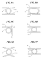
- FIGS. 9A-F are schematic views of different types of resonators: FIG. 9A depicts a circular resonator, FIG. 9B depicts an elliptical resonator; FIG. 9C depicts a resonator having perpendicular input and output waveguides; FIG. 9D depicts a zero-gap coupling resonator; FIG. 9E shows a resonator having curved input and output waveguides; and FIG. 9F depicts a vertical gap coupling resonator.
- light signal and “optical signal” are used interchangeably, and may include signals such as WDM, DWDM, UDWDM signals, and the like.
- the terms “light”, “light signal” and optical signal” are intended to be broadly construed and to refer to visible, infrared, ultraviolet light, and the like.
- An important feature of this invention is the use of a very compact electric heater which can provide efficient, localized heating of an optical resonator.
- This heater could be realized in a variety of ways, such as a forward-biased or p-i-n junction, which is shown in FIGS. 4A and 4B, and a surface resistance heater, which is shown in FIGS. 5 and 6. Each of these heater constructions will be discussed in turn.
- FIGS. 4A, 5 and 6 depict various aspects of a coupler 101 , 201 , 301 incorporating a tunable ring resonator 5 constructed in accordance with one embodiment of this invention.
- Each coupler 101 , 201 , 301 includes an input waveguide 9 from which light may be coupled into the resonator 5 , an output waveguide 11 to which light may couple out from the resonator 5 , and, of course, the resonator 5 itself.
- the resonator 5 differs from conventional ring resonators in that it includes a localized heater structure.
- light traveling along input waveguide 9 in the direction of arrows A is either output from the coupler 101 through input waveguide 9 or, if the light has the proper wavelength for coupling to the resonator 5 , coupled and output through output waveguide 11 in the direction of arrow B.
- the shapes and orientations of the input and output waveguides 9 , 11 as shown in FIG. 4A are only exemplary; either or both of these waveguides 9 , 11 can be straight or curved. Nor do those waveguides 9 , 11 have to be parallel to each other.
- FIGS. 4A and 4B depict a cylindrical and annular components
- the present invention is not to be limited to such shapes.
- different shaped resonators 5 could be employed.
- Correspondingly-shaped non-circular components also could be used.
- the tunable resonator 5 used in coupler 101 operates in a manner comparable to known resonators.
- the wavelength of the optical signal propagating though the input waveguide 9 is the same as the ring resonator's resonance wavelength, the signal couples from the input waveguide 9 to resonator 5 and from the resonator 5 into the output waveguide 11 . Otherwise, the optical signal continues propagating through the input waveguide 9 .
- the amount of signal; coupled by the coupler 101 into and out of the resonator body 5 is controlled by three variables: coupling between the input waveguide 9 and the resonator 5 , coupling between the resonator 5 and the output waveguide 11 ; and by the losses in the resonator.
- a diode junction heater 103 is provided to tune resonator 5 .
- Diode junction heater 103 has a cylindrical disk 15 formed within resonator 5 .
- the cylindrical disk 15 is separated from the resonator 5 by cylindrical trench 13 .
- the cylindrical disk 15 , cylindrical trench 13 and resonator 5 are all arranged concentrically about a common center point (not shown).
- a diode 103 may be formed as an integral part of the structure of the coupler 101 .
- the present invention is not intended to be limited to circular and annular components—the terms “cylindrical disk”, “cylindrical trench” and “ring” are used by way of example only, and not limitation. These terms, and the terms “disk” and “ring” are to be construed broadly and are meant to cover any shapes which can serve in an optical resonator, which other shapes are equivalents thereto.
- diode junction heater 103 is a layered structure arranged as follows.
- a core layer 29 is sandwiched between an upper cladding layer 25 and a lower cladding layer 27 , which also serves as a substrate.
- the core layer 29 is formed of a material having a higher refractive index than the surrounding cladding layers 25 , 27 .
- a separate substrate could be provided, and such a substrate could be made, for example, from silicon or quartz.
- the cylindrical trench 13 formed in the diode junction heater 103 is sufficiently deep to extend completely through the upper cladding layer 25 and the core layer 29 , and part of the way through the lower cladding layer 27 .
- the cylindrical trench 13 can be formed using any suitable manufacturing technique, preferably by etching a ring-shaped trench into a disk-shaped resonator (not-shown). This results in formation of both the cylindrical disk 15 and the ring resonator 5 .
- the cylindrical disk 15 , cylindrical trench 13 and resonator 5 are coated with a leveling material 30 .
- the leveling material 30 is applied to fill completely the cylindrical trench 13 and to cover all of the resonator 5 .
- the center of the cylindrical disk 15 preferably is not covered by the leveling material 30 , this having been done in order to facilitate electrical contact with the heater 103 .
- Leveling material 30 has optical properties which do not prevent confinement of light within the waveguides 9 , 11 or resonator 5 .
- Leveling material 30 is preferably made from BCB/polyimide or SiO 2 /Si 3 N 4 .
- top electrode 19 is applied atop the cylindrical disk 15 where the center of the cylindrical disk 15 is not covered by leveling material 30 .
- Top electrode 19 is preferably arranged so as not to overlap the optical field defined by the resonator 5 . This way, there is no added loss, which is polarization dependent due to absorption by the top electrode 19 .
- Top electrode 19 is electrically connected to a surface-mounted contact pad 17 , which rests atop leveling material 30 .
- the contact pad 17 is positioned some distance from the resonator 5 .
- a bottom electrode 21 provides electrical contact with the underside of the lower cladding layer 27 and completes a circuit with top electrode 19 through which current, generally designated as I, may flow.
- the upper cladding layer 25 , the core layer 29 , and the lower cladding layer 27 are doped to form a forward-biased or P-I-N semiconductor layer structure. This can be accomplished using p-type, n-type or intrinsic doping. It is presently thought to be preferred to have low or intrinsic doping in the waveguide core layer 29 to minimize the free optical carrier absorption losses. It will be understood that each of these cladding and core layers 25 , 27 , 29 should be made from semiconductor material such as GaAs, InP and Si.
- the diode junction heater 103 To energize the diode junction heater 103 , current is applied through top electrode 19 and flows through the cylindrical disk 15 to the bottom electrode 21 . The current passing through the forwardly-biased p-i-n structure will generate heat in the diode. That heat will be dissipated in the diode and conducted laterally across trench 13 to the ring resonator 5 . This heat flow will be affected in part by the size of the cylindrical trench 13 separating the cylindrical disk 15 and the resonator 5 , as well as by the thermal conductivity of the leveling material 30 in the cylindrical trench 13 . It is presently thought to be preferable for the cylindrical trench 13 to be no more than several microns in radius so as to maximize thermal conduction therethrough.
- This system for the thermal tuning of optical resonators can be used in devices having waveguide systems made from semiconductors (GaAs, InP, Si), since doped junctions (p-type, intrinsic or n-type) can only be implemented in semiconductor materials.
- core layer 29 is preferably made from InP- or GaAs-based waveguide materials.
- Upper cladding layer 25 is preferably made from InP- or GaAs-based waveguide materials.
- Lower cladding layer 27 is preferably made from InP- or GaAs-based waveguide materials. While a forward-biased p-i-n device such as diode junction heater 103 can be used for heat generating, such a device may not always be an efficient thermal source.
- the electrical power that is applied to the diode junction heater 103 will in part be wasted generating photons (especially for direct bandgap semiconductors such as GaAs and InP) in addition to heating resistive regions of the diode junction heater 103 .
- photons especially for direct bandgap semiconductors such as GaAs and InP
- significant heat is likely to be generated by p-type ohmic contact. Consequently, the following further embodiments of this invention have been developed.
- the coupler 201 shown in FIG. 5 includes, in addition to input waveguide 9 , output waveguide 11 , and resonator 5 , a thin-film surface resistance heater 203 .
- the thin film surface resistance heater 203 is formed by placing a resistive element 31 between two terminating electrical contact pads 117 , 217 .
- the heater 203 is energized by passing electrical current between the two contact pads 117 , 217 , so that the current flows through the resistive element 31 .
- This preferred design of the heater 203 employs a serpentine resistive element 31 , since this maximizes resistance between the two contact pads 117 , 217 .
- the resistance of the heater 203 can be increased by maximizing the length of the conductor serpentine resistive element 31 between the contact pads 117 , 217 (hence the serpentine shape) and by minimizing the trace width and film thickness.
- the material used for the serpentine resistive element 31 should be conductive and also have high resistivity.
- such materials could include but are not limited to NiCr, Cr or C. It should be noted that these materials differ from the contact pad material, which is preferably made of Au because of its high conductivity, wire bondability, and high oxidation resistance.
- the serpentine resistive element 31 overlaps the resonator 5 .
- overlaps is used in its broadest sense, and does not require every part of resonator 5 be covered by a portion of the serpentine resistive element 31 .
- this drawing shows a serpentine resistive element 31 , which can be said to cover the resonator 5 with substantial uniformity, substantial portions of resonator 5 could be left exposed; nor need the resonator 5 be covered evenly or symmetrically.
- a further advantage of the surface resistance heater 203 is that it may be utilized with any type of waveguide structure and material. This includes, but is not limited to, the use of optical waveguides fabricated from semiconductors, silica glass, polymers and lithium niobate.
- FIG. 6 depicts an embodiment of this invention which can effect such local monitoring and heating.
- Coupler 301 shown in FIG. 6 includes a resonator 5 having a heater 303 with a serpentine resistive element 31 which can be energized through contact pads 117 , 217 , and which is comparable to that shown in FIG. 5 .
- a bimetallic thermocouple 41 superimposed on this structure is a bimetallic thermocouple 41 , which consists of two dissimilar metal films 35 , 37 . These films 35 , 37 are shaped with relatively narrow tongues 43 , 43 ′ and relatively wide contacts 45 , 45 ′.
- the tongues 43 , 43 ′ form an overlapping junction 33 over the resonator 5 .
- thermocouple 41 A suitable insulator dielectric (not shown), such as SiO 2 , is applied between the thermocouple 41 and serpentine resistive element 31 to prevent electrical short circuits between these components.
- Thermocouple 41 could be formed in a known manner from a wide variety of dissimilar materials, such as copper, chrome, iron, or Constantan (a known Cu/Ni alloy).
- a voltage closely corresponding to the temperature will be formed at the overlapping junction 33 of the thermocouple 41 . This voltage can be detected by measuring the difference in potential between contact 45 and contact 45 ′. Since the voltage closely correlates to the temperature of the junction 33 , the temperature of the junction 33 can be accurately determined and the serpentine resistive element 31 can be energized accordingly.
- that temperature could be closely regulated using a feedback loop to control energization of the serpentine resistive element 31 .
- FIGS. 9A-F depict examples of different resonator and waveguide coupling configurations in which the present invention could be used, such as the elliptical resonator depicted in FIG. 9B, the resonator having perpendicular input and output guides of FIG. 9C, the zero-gap coupling resonator depicted in FIG. 9D, the resonator having both curved inputs and outputs of FIG. 9E, and the vertical gap coupling resonator of FIG. 9 F.
- these resonators are all considered as being equivalent to a ring resonator.
- the present invention could be used with all types of self-feeding resonators.
- the diode heater 103 may be used with any semiconductor waveguide material, including by way of example only and not limitation, Si, GaAs and InP.
- the surface resistance heater 203 , 303 may be used with waveguides of nearly any type of waveguide material, including by way of example only and not limitation, semiconductors, silica glass, polymers and lithium niobate.
- the core layer 29 can be rectangular, with sides running from approximately 3-10 ⁇ m thick and approximately 3-15 ⁇ m wide. More preferably, the core layer 29 is square, with sides from approximately 6-8 ⁇ m thick and approximately 6-14 ⁇ m wide.
- the upper and lower cladding layers 25 , 27 adjacent to core layer 29 can be approximately 3-18 ⁇ m thick, and are preferably approximately 15 ⁇ m thick. While a wide variety of materials can be used to make the core and cladding layers, silica is presently preferred.
- the present thermal tuning invention is applicable to both strongly confined and weakly confined optical waveguides.
- the use of weakly-confined waveguides is presently preferred.
- FIG. 7 A cross-section of a passive waveguide structure is depicted in FIG. 7, and includes a core layer 29 , sandwiched between an upper cladding layer 25 and a lower cladding layer 27 .
- the entire assembly can rest upon a substrate 24 .
- This invention is not to be limited thereto, and can for example also be used in an active architecture as a laser.
- the resonator 5 includes an active layer 39 of material which provides gain.
- the active layer 39 can be made from a wide variety of materials. Active layer 39 is sandwiched core layers 29 , which core layers 29 are in turn sandwiched between an upper cladding layer 25 and a lower cladding layer 27 .
- the entire assembly can rest upon a substrate 24 .
Abstract
Description


Claims (17)
Priority Applications (1)
| Application Number | Priority Date | Filing Date | Title |
|---|---|---|---|
| US09/718,662 US6636668B1 (en) | 1999-11-23 | 2000-11-22 | Localized thermal tuning of ring resonators |
Applications Claiming Priority (2)
| Application Number | Priority Date | Filing Date | Title |
|---|---|---|---|
| US16713999P | 1999-11-23 | 1999-11-23 | |
| US09/718,662 US6636668B1 (en) | 1999-11-23 | 2000-11-22 | Localized thermal tuning of ring resonators |
Publications (1)
| Publication Number | Publication Date |
|---|---|
| US6636668B1 true US6636668B1 (en) | 2003-10-21 |
Family
ID=22606097
Family Applications (1)
| Application Number | Title | Priority Date | Filing Date |
|---|---|---|---|
| US09/718,662 Expired - Lifetime US6636668B1 (en) | 1999-11-23 | 2000-11-22 | Localized thermal tuning of ring resonators |
Country Status (4)
| Country | Link |
|---|---|
| US (1) | US6636668B1 (en) |
| AU (1) | AU1795201A (en) |
| TW (1) | TW508461B (en) |
| WO (1) | WO2001038905A2 (en) |
Cited By (66)
| Publication number | Priority date | Publication date | Assignee | Title |
|---|---|---|---|---|
| US20030059190A1 (en) * | 2001-09-10 | 2003-03-27 | Gunn Lawrence Cary | Strip loaded waveguide with low-index transition layer |
| US20030068134A1 (en) * | 2001-09-10 | 2003-04-10 | Gunn Lawrence Cary | Tuning the index of a waveguide structure |
| US20030068152A1 (en) * | 2001-09-10 | 2003-04-10 | Gunn Lawrence Cary | Structure and method for coupling light between dissimilar waveguides |
| US20040020463A1 (en) * | 2002-07-31 | 2004-02-05 | Anderson Michael D. | Pump and hydraulic system with low pressure priming and over pressurization avoidance features |
| US20060051010A1 (en) * | 2002-12-27 | 2006-03-09 | Sai Chu | Coupled optical waveguide resonators with heaters for thermo-optic control of wavelength and compound filter shape |
| US20060153267A1 (en) * | 2005-01-11 | 2006-07-13 | Nec Corporation | Multiple resonator and variable-wavelength light source using the same |
| US20060198416A1 (en) * | 2005-03-03 | 2006-09-07 | Nec Corporation | Wavelength tunable laser |
| US20060239616A1 (en) * | 2005-04-26 | 2006-10-26 | Harris Coporation | Optical microresonator with coupling elements for changing light direction |
| US20060239617A1 (en) * | 2005-04-26 | 2006-10-26 | Harris Corporation | Optical microresonator with microcylinder and circumferential coating forming resonant waveguides |
| US20060280407A1 (en) * | 2005-04-26 | 2006-12-14 | Harris Corporation | Spiral waveguide slow wave resonator structure |
| US20070071394A1 (en) * | 2003-12-24 | 2007-03-29 | Faccio Daniele F A | Low loss microring resonator device |
| US20070223859A1 (en) * | 2006-03-27 | 2007-09-27 | Hewlett-Packard Development Company Lp | Resonators |
| US20070223866A1 (en) * | 2006-03-22 | 2007-09-27 | Searete Llc, A Limited Liability Corporation Of The State Of Delaware | Controllable electromagnetically responsive assembly of self resonant bodies |
| US20070230856A1 (en) * | 2006-03-30 | 2007-10-04 | Nec Corporation | Variable light controlling device and variable light controlling method |
| US7310459B1 (en) * | 2005-10-25 | 2007-12-18 | Xilinx, Inc. | On-chip programmable optical crossbar switch |
| US7315679B2 (en) | 2004-06-07 | 2008-01-01 | California Institute Of Technology | Segmented waveguide structures |
| US20080031296A1 (en) * | 2006-07-27 | 2008-02-07 | Sean Spillane | Scalable and defect-tolerant quantum-dot-based quantum computer architectures and methods for fabricating quantum dots in quantum computer architectures |
| US20080153262A1 (en) * | 2006-12-22 | 2008-06-26 | Stats Chippac Ltd. | Wafer system with partial cuts |
| US7424187B2 (en) | 2005-04-26 | 2008-09-09 | Harris Corporation | Optical microresonator with resonant waveguide imparting polarization |
| US7466881B1 (en) * | 2007-07-13 | 2008-12-16 | Hewlett-Packard Development Company, L.P. | Optical switch |
| US20090046976A1 (en) * | 2006-03-22 | 2009-02-19 | Hillis Daniel W | High-Q resonators assembly |
| US20090103854A1 (en) * | 2007-10-23 | 2009-04-23 | Beausoleil Raymond G | Photonic interconnects for computer system devices |
| US20090103345A1 (en) * | 2007-10-23 | 2009-04-23 | Mclaren Moray | Three-dimensional memory module architectures |
| US20090103855A1 (en) * | 2007-10-23 | 2009-04-23 | Nathan Binkert | Three-dimensional die stacks with inter-device and intra-device optical interconnect |
| US20090110348A1 (en) * | 2007-10-31 | 2009-04-30 | Alexandre Bratkovski | Magnetically Activated Photonic Switches And Switch Fabrics Employing The Same |
| US20090152259A1 (en) * | 2007-12-17 | 2009-06-18 | Momentive Performance Materials Inc. | Electrode tuning method and apparatus for a layered heater structure |
| US20090169149A1 (en) * | 2007-12-27 | 2009-07-02 | Bruce Andrew Block | Stabilized ring resonator modulator |
| JP2009169281A (en) * | 2008-01-18 | 2009-07-30 | Toshiba Corp | Optical multiplexer/demultiplexer |
| US20090208162A1 (en) * | 2008-02-14 | 2009-08-20 | Hrl Laboratories, Llc | Unit-cell array optical signal processor |
| WO2009113977A1 (en) * | 2008-03-11 | 2009-09-17 | Hewlett-Packard Development Company, L.P. | Optoelectronic switches using on-chip optical waveguides |
| US20100098372A1 (en) * | 2006-08-24 | 2010-04-22 | Cornell Research Foundation, Inc | Electro-optical modulator |
| WO2010108093A2 (en) * | 2009-03-20 | 2010-09-23 | Cornell University | Apparatus and methods for wide temperature range operation of micrometer-scale silicon electro-optic modulators |
| US7826688B1 (en) | 2005-10-21 | 2010-11-02 | Luxtera, Inc. | Enhancing the sensitivity of resonant optical modulating and switching devices |
| WO2011081638A2 (en) * | 2009-12-15 | 2011-07-07 | Kotura, Inc. | Ring resonator with wavelength selectivity |
| US20110190167A1 (en) * | 2006-03-22 | 2011-08-04 | Hillis W Daniel | Electromagnetically responsive element with self resonant bodies |
| US20120105177A1 (en) * | 2010-10-29 | 2012-05-03 | Mclaren Moray | Resonator systems and methods for tuning resonator systems |
| US20120251107A1 (en) * | 2002-08-15 | 2012-10-04 | Krug William P | WDM Router |
| US20120301068A1 (en) * | 2011-05-27 | 2012-11-29 | Micron Technology, Inc. | Optical waveguide with cascaded modulator circuits |
| US8334797B1 (en) | 2010-04-20 | 2012-12-18 | Hrl Laboratories, Llc | Wideband high resolution time-stretched photonic analog-to-digital converter |
| US20130037692A1 (en) * | 2011-08-10 | 2013-02-14 | Fujitsu Limited | Optical semiconductor device |
| US20140185982A1 (en) * | 2011-07-29 | 2014-07-03 | University Court Of The University Of St Andrews | Wave vector matched resonator and bus waveguide system |
| US20140328591A1 (en) * | 2012-07-26 | 2014-11-06 | Brian Koch | Reconfigurable optical transmitter |
| US9063354B1 (en) | 2012-02-07 | 2015-06-23 | Sandia Corporation | Passive thermo-optic feedback for robust athermal photonic systems |
| US9081135B1 (en) * | 2013-08-27 | 2015-07-14 | Sandia Corporation | Methods and devices for maintaining a resonant wavelength of a photonic microresonator |
| WO2015160495A1 (en) * | 2014-04-16 | 2015-10-22 | Micron Technology, Inc. | Method and apparatus providing compensation for wavelength drift in photonic structures |
| US9195113B2 (en) | 2012-05-25 | 2015-11-24 | Honeywell International Inc. | Tunable multispectral laser source |
| US20150381301A1 (en) * | 2013-03-22 | 2015-12-31 | Fujitsu Limited | Wavelength division multiplexing optical receiver |
| US20150381277A1 (en) * | 2014-06-30 | 2015-12-31 | Fujitsu Limited | Optical transmission system, transmitter, receiver, and optical transmission method |
| US20160131926A1 (en) * | 2013-06-18 | 2016-05-12 | Suzhou Institute Of Nano-Tech And Nano-Bionics Of Chinese Academy Of Science | Ring Cavity Device and its Fabrication Method Thereof |
| US9366822B1 (en) | 2015-09-29 | 2016-06-14 | Sandia Corporation | Thermo-optically tuned photonic resonators with concurrent electrical connection and thermal isolation |
| US9400402B2 (en) | 2014-01-07 | 2016-07-26 | Electronics And Telecommunications Research Institute | Optical waveguide and optical device based on the same |
| US9438263B1 (en) | 2014-05-02 | 2016-09-06 | Hrl Laboratories, Llc | Controllable opto-electronic time stretcher, an electro-optical analog to digital converter having non-uniform sampling using the same, and related methods of operation |
| US20170017039A1 (en) * | 2014-03-28 | 2017-01-19 | Huawei Technologies Co., Ltd. | Optical Interconnector, Optoelectronic Chip System, and Optical Signal Sharing Method |
| US9612458B1 (en) * | 2014-04-23 | 2017-04-04 | Sandia Corporation | Resonant optical device with a microheater |
| US9819435B2 (en) | 2010-08-26 | 2017-11-14 | Cornell University | Optical apparatus, method, and applications |
| US20170336657A1 (en) * | 2014-11-18 | 2017-11-23 | Nec Corporation | A heater for optical waveguide and a method for configuring a heater for optical waveguide |
| WO2018166327A1 (en) | 2017-03-14 | 2018-09-20 | Huawei Technologies Co., Ltd. | Optical device |
| US10162117B2 (en) * | 2008-09-05 | 2018-12-25 | Morton Photonics | Uncooled operation of microresonator devices |
| USD840404S1 (en) | 2013-03-13 | 2019-02-12 | Nagrastar, Llc | Smart card interface |
| US10382816B2 (en) | 2013-03-13 | 2019-08-13 | Nagrastar, Llc | Systems and methods for performing transport I/O |
| CN110174781A (en) * | 2019-05-06 | 2019-08-27 | 吉林师范大学 | A kind of reticular structure micro-loop electro-optical switch array device |
| CN110221458A (en) * | 2019-05-06 | 2019-09-10 | 吉林师范大学 | A kind of micro-loop electro-optical switch array device with wavelength conversion characteristics |
| USD864968S1 (en) | 2015-04-30 | 2019-10-29 | Echostar Technologies L.L.C. | Smart card interface |
| US10935817B2 (en) * | 2018-10-01 | 2021-03-02 | Electronics And Telecommunications Research Institute | Optical device and driving method thereof |
| USRE48654E1 (en) * | 2014-11-05 | 2021-07-20 | Nokia Solutions & Networks Oy | Photonic integrated circuit incorporating a bandgap temperature sensor |
| US20220026634A1 (en) * | 2020-07-16 | 2022-01-27 | Board Of Trustees Of The University Of Illinois | Resonant-based photonic intensity modulators integrated with fully etched thin-film lithium niobate waveguides |
Families Citing this family (10)
| Publication number | Priority date | Publication date | Assignee | Title |
|---|---|---|---|---|
| US7103245B2 (en) | 2000-07-10 | 2006-09-05 | Massachusetts Institute Of Technology | High density integrated optical chip |
| GB2376532A (en) * | 2001-06-15 | 2002-12-18 | Kymata Ltd | Thermally controlled optical resonator |
| US6934427B2 (en) | 2002-03-12 | 2005-08-23 | Enablence Holdings Llc | High density integrated optical chip with low index difference waveguide functions |
| US20040114867A1 (en) * | 2002-12-17 | 2004-06-17 | Matthew Nielsen | Tunable micro-ring filter for optical WDM/DWDM communication |
| JP3692354B2 (en) * | 2002-12-26 | 2005-09-07 | 独立行政法人科学技術振興機構 | Electromagnetic frequency filter |
| US7236679B2 (en) * | 2005-04-26 | 2007-06-26 | Harris Corporation | Optical microresonator coupling system and associated method |
| US7848599B2 (en) * | 2009-03-31 | 2010-12-07 | Oracle America, Inc. | Optical device with large thermal impedance |
| CN102285623A (en) * | 2011-04-21 | 2011-12-21 | 中国科学院半导体研究所 | Micro-nano biosensor with double-ring structure and manufacturing method thereof |
| DE102013213138A1 (en) * | 2013-07-04 | 2015-01-08 | Zumtobel Lighting Gmbh | Illumination arrangement with laser as light source |
| CN109001158B (en) * | 2018-06-22 | 2020-10-02 | 东南大学 | Nano sensor based on double-inner-gear annular cavity |
Citations (2)
| Publication number | Priority date | Publication date | Assignee | Title |
|---|---|---|---|---|
| WO2001027692A1 (en) | 1999-10-14 | 2001-04-19 | Lambda Crossing Ltd. | An integrated optical device for data communication |
| US6411752B1 (en) * | 1999-02-22 | 2002-06-25 | Massachusetts Institute Of Technology | Vertically coupled optical resonator devices over a cross-grid waveguide architecture |
Family Cites Families (3)
| Publication number | Priority date | Publication date | Assignee | Title |
|---|---|---|---|---|
| US4782492A (en) * | 1986-05-05 | 1988-11-01 | Polaroid Corporation | Thermally controllable optical devices and system |
| DE4231177A1 (en) * | 1992-09-17 | 1994-03-24 | Siemens Ag | Semiconductor laser used as FM transmitter for optical communications - has charge-injection diode, and heating diode formed from simple pn junction with separate contacts form those used for carrying laser current |
| EP0915353B1 (en) * | 1997-10-31 | 2005-08-10 | Infineon Technologies AG | Optical waveguide arrangement |
-
2000
- 2000-11-22 WO PCT/US2000/032189 patent/WO2001038905A2/en active Application Filing
- 2000-11-22 US US09/718,662 patent/US6636668B1/en not_active Expired - Lifetime
- 2000-11-22 AU AU17952/01A patent/AU1795201A/en not_active Abandoned
- 2000-11-22 TW TW089124827A patent/TW508461B/en not_active IP Right Cessation
Patent Citations (2)
| Publication number | Priority date | Publication date | Assignee | Title |
|---|---|---|---|---|
| US6411752B1 (en) * | 1999-02-22 | 2002-06-25 | Massachusetts Institute Of Technology | Vertically coupled optical resonator devices over a cross-grid waveguide architecture |
| WO2001027692A1 (en) | 1999-10-14 | 2001-04-19 | Lambda Crossing Ltd. | An integrated optical device for data communication |
Cited By (147)
| Publication number | Priority date | Publication date | Assignee | Title |
|---|---|---|---|---|
| US7127147B2 (en) | 2001-09-10 | 2006-10-24 | California Institute Of Technology | Strip loaded waveguide with low-index transition layer |
| US20030059190A1 (en) * | 2001-09-10 | 2003-03-27 | Gunn Lawrence Cary | Strip loaded waveguide with low-index transition layer |
| US20030068134A1 (en) * | 2001-09-10 | 2003-04-10 | Gunn Lawrence Cary | Tuning the index of a waveguide structure |
| US20030063885A1 (en) * | 2001-09-10 | 2003-04-03 | Gunn Lawrence Cary | Electronically biased strip loaded waveguide |
| US20030068152A1 (en) * | 2001-09-10 | 2003-04-10 | Gunn Lawrence Cary | Structure and method for coupling light between dissimilar waveguides |
| US20030068132A1 (en) * | 2001-09-10 | 2003-04-10 | Gunn Lawrence Cary | Tunable resonant cavity based on the field effect in semiconductors |
| US7203403B2 (en) * | 2001-09-10 | 2007-04-10 | California Institute Of Technology | Modulator based on tunable resonant cavity |
| US6834152B2 (en) | 2001-09-10 | 2004-12-21 | California Institute Of Technology | Strip loaded waveguide with low-index transition layer |
| US6839488B2 (en) | 2001-09-10 | 2005-01-04 | California Institute Of Technology | Tunable resonant cavity based on the field effect in semiconductors |
| US6895148B2 (en) * | 2001-09-10 | 2005-05-17 | California Institute Of Technology | Modulator based on tunable resonant cavity |
| US20050123259A1 (en) * | 2001-09-10 | 2005-06-09 | Gunn Lawrence C.Iii | Strip loaded waveguide integrated with electronics components |
| US6917727B2 (en) | 2001-09-10 | 2005-07-12 | California Institute Of Technology | Strip loaded waveguide integrated with electronics components |
| US6990257B2 (en) | 2001-09-10 | 2006-01-24 | California Institute Of Technology | Electronically biased strip loaded waveguide |
| US7167606B2 (en) | 2001-09-10 | 2007-01-23 | California Institute Of Technology | Electronically biased strip loaded waveguide |
| US7164821B2 (en) | 2001-09-10 | 2007-01-16 | California Institute Of Technology | Tunable resonant cavity based on the field effect in semiconductors |
| US7082235B2 (en) | 2001-09-10 | 2006-07-25 | California Institute Of Technology | Structure and method for coupling light between dissimilar waveguides |
| US20030068131A1 (en) * | 2001-09-10 | 2003-04-10 | Gunn Lawrence C. | Modulator based on tunable resonant cavity |
| US7120338B2 (en) | 2001-09-10 | 2006-10-10 | California Institute Of Technology | Tuning the index of a waveguide structure |
| US20040020463A1 (en) * | 2002-07-31 | 2004-02-05 | Anderson Michael D. | Pump and hydraulic system with low pressure priming and over pressurization avoidance features |
| US20120251107A1 (en) * | 2002-08-15 | 2012-10-04 | Krug William P | WDM Router |
| US10425706B2 (en) * | 2002-08-15 | 2019-09-24 | The Boeing Company | WDM router |
| US20060051010A1 (en) * | 2002-12-27 | 2006-03-09 | Sai Chu | Coupled optical waveguide resonators with heaters for thermo-optic control of wavelength and compound filter shape |
| US20070071394A1 (en) * | 2003-12-24 | 2007-03-29 | Faccio Daniele F A | Low loss microring resonator device |
| US7315679B2 (en) | 2004-06-07 | 2008-01-01 | California Institute Of Technology | Segmented waveguide structures |
| US20060153267A1 (en) * | 2005-01-11 | 2006-07-13 | Nec Corporation | Multiple resonator and variable-wavelength light source using the same |
| US7389028B2 (en) * | 2005-01-11 | 2008-06-17 | Nec Corporation | Multiple resonator and variable-wavelength light source using the same |
| US20060198416A1 (en) * | 2005-03-03 | 2006-09-07 | Nec Corporation | Wavelength tunable laser |
| US7664156B2 (en) * | 2005-03-03 | 2010-02-16 | Nec Corporation | Wavelength tunable laser |
| US7346241B2 (en) * | 2005-04-26 | 2008-03-18 | Harris Corporation | Optical microresonator with microcylinder and circumferential coating forming resonant waveguides |
| US20060239617A1 (en) * | 2005-04-26 | 2006-10-26 | Harris Corporation | Optical microresonator with microcylinder and circumferential coating forming resonant waveguides |
| US7555179B2 (en) | 2005-04-26 | 2009-06-30 | Harris Corporation | Optical microresonator with resonant waveguide imparting polarization |
| US20080273828A1 (en) * | 2005-04-26 | 2008-11-06 | Harris Corporation | Optical microresonator with resonant waveguide imparting polarization |
| US7286734B2 (en) | 2005-04-26 | 2007-10-23 | Harris Corporation | Optical microresonator with coupling elements for changing light direction |
| US7424187B2 (en) | 2005-04-26 | 2008-09-09 | Harris Corporation | Optical microresonator with resonant waveguide imparting polarization |
| US20060280407A1 (en) * | 2005-04-26 | 2006-12-14 | Harris Corporation | Spiral waveguide slow wave resonator structure |
| US20060239616A1 (en) * | 2005-04-26 | 2006-10-26 | Harris Coporation | Optical microresonator with coupling elements for changing light direction |
| US7415178B2 (en) | 2005-04-26 | 2008-08-19 | Harris Corporation | Spiral waveguide slow wave resonator structure |
| US7973265B2 (en) * | 2005-08-19 | 2011-07-05 | Infinera Corporation | Coupled optical waveguide resonators with heaters for thermo-optic control of wavelength and compound filter shape |
| US7356221B2 (en) * | 2005-08-19 | 2008-04-08 | Infinera Corporation | Coupled optical waveguide resonators with heaters for thermo-optic control of wavelength and compound filter shape |
| US20090314763A1 (en) * | 2005-08-19 | 2009-12-24 | Sai Chu | Coupled optical waveguide resonators with heaters for thermo-optic control of wavelength and compound filter shape |
| US20080175538A1 (en) * | 2005-08-19 | 2008-07-24 | Sai Chu | Coupled optical waveguide resonators with heaters for thermo-optic control of wavelength and compound filter shape |
| US7583879B2 (en) * | 2005-08-19 | 2009-09-01 | Infinera Corporation | Coupled optical waveguide resonators with heaters for thermo-optic control of wavelength and compound filter shape |
| US7903910B2 (en) * | 2005-08-19 | 2011-03-08 | Infinera Corporation | Coupled optical waveguide resonators with heaters for thermo-optic control of wavelength and compound filter shape |
| US20070211992A1 (en) * | 2005-08-19 | 2007-09-13 | Sai Chu | Coupled optical waveguide resonators with heaters for thermo-optic control of wavelength and compound filter shape |
| US20070206899A1 (en) * | 2005-08-19 | 2007-09-06 | Sai Chu | Coupled optical waveguide resonators with heaters for thermo-optic control of wavelength and compound filter shape |
| US7231113B2 (en) * | 2005-08-19 | 2007-06-12 | Infinera Corporation | Coupled optical waveguide resonators with heaters for thermo-optic control of wavelength and compound filter shape |
| US7826688B1 (en) | 2005-10-21 | 2010-11-02 | Luxtera, Inc. | Enhancing the sensitivity of resonant optical modulating and switching devices |
| US7310459B1 (en) * | 2005-10-25 | 2007-12-18 | Xilinx, Inc. | On-chip programmable optical crossbar switch |
| US20110190167A1 (en) * | 2006-03-22 | 2011-08-04 | Hillis W Daniel | Electromagnetically responsive element with self resonant bodies |
| US20090046976A1 (en) * | 2006-03-22 | 2009-02-19 | Hillis Daniel W | High-Q resonators assembly |
| US8369659B2 (en) * | 2006-03-22 | 2013-02-05 | The Invention Science Fund I Llc | High-Q resonators assembly |
| US8358881B2 (en) * | 2006-03-22 | 2013-01-22 | The Invention Science Fund I Llc | High-Q resonators assembly |
| US20090022455A1 (en) * | 2006-03-22 | 2009-01-22 | Searete Llc, A Limited Liability Corporation Of The State Of Delaware | High-Q resonators assembly |
| US20070223866A1 (en) * | 2006-03-22 | 2007-09-27 | Searete Llc, A Limited Liability Corporation Of The State Of Delaware | Controllable electromagnetically responsive assembly of self resonant bodies |
| US20070223859A1 (en) * | 2006-03-27 | 2007-09-27 | Hewlett-Packard Development Company Lp | Resonators |
| US7729576B2 (en) * | 2006-03-27 | 2010-06-01 | Hewlett-Packard Development Company, L.P. | Modulated signal resonators |
| US20070230856A1 (en) * | 2006-03-30 | 2007-10-04 | Nec Corporation | Variable light controlling device and variable light controlling method |
| US7440643B2 (en) * | 2006-03-30 | 2008-10-21 | Nec Corporation | Variable light controlling device and variable light controlling method |
| US20080031296A1 (en) * | 2006-07-27 | 2008-02-07 | Sean Spillane | Scalable and defect-tolerant quantum-dot-based quantum computer architectures and methods for fabricating quantum dots in quantum computer architectures |
| US7529437B2 (en) * | 2006-07-27 | 2009-05-05 | Hewlett-Packard Development Company, L.P. | Scalable and defect-tolerant quantum-dot-based quantum computer architectures and methods for fabricating quantum dots in quantum computer architectures |
| US20100098372A1 (en) * | 2006-08-24 | 2010-04-22 | Cornell Research Foundation, Inc | Electro-optical modulator |
| US8295655B2 (en) | 2006-08-24 | 2012-10-23 | Cornell Research Foundation, Inc. | Electro-optical modulator |
| US20080153262A1 (en) * | 2006-12-22 | 2008-06-26 | Stats Chippac Ltd. | Wafer system with partial cuts |
| US7466881B1 (en) * | 2007-07-13 | 2008-12-16 | Hewlett-Packard Development Company, L.P. | Optical switch |
| US7532785B1 (en) | 2007-10-23 | 2009-05-12 | Hewlett-Packard Development Company, L.P. | Photonic interconnects for computer system devices |
| US8059443B2 (en) | 2007-10-23 | 2011-11-15 | Hewlett-Packard Development Company, L.P. | Three-dimensional memory module architectures |
| US20090103854A1 (en) * | 2007-10-23 | 2009-04-23 | Beausoleil Raymond G | Photonic interconnects for computer system devices |
| US20090103345A1 (en) * | 2007-10-23 | 2009-04-23 | Mclaren Moray | Three-dimensional memory module architectures |
| US20090103855A1 (en) * | 2007-10-23 | 2009-04-23 | Nathan Binkert | Three-dimensional die stacks with inter-device and intra-device optical interconnect |
| US20090274413A1 (en) * | 2007-10-23 | 2009-11-05 | Beausoleil Raymond G | Photonic interconnects for computer system devices |
| US7889956B2 (en) | 2007-10-23 | 2011-02-15 | Hewlett-Packard Development Company, L.P. | Photonic interconnects for computer system devices |
| US8064739B2 (en) | 2007-10-23 | 2011-11-22 | Hewlett-Packard Development Company, L.P. | Three-dimensional die stacks with inter-device and intra-device optical interconnect |
| US20090110348A1 (en) * | 2007-10-31 | 2009-04-30 | Alexandre Bratkovski | Magnetically Activated Photonic Switches And Switch Fabrics Employing The Same |
| US8009943B2 (en) * | 2007-10-31 | 2011-08-30 | Hewlett-Packard Development Company, L.P. | Magnetically activated photonic switches and switch fabrics employing the same |
| US7777160B2 (en) | 2007-12-17 | 2010-08-17 | Momentive Performance Materials Inc. | Electrode tuning method and apparatus for a layered heater structure |
| US20090152259A1 (en) * | 2007-12-17 | 2009-06-18 | Momentive Performance Materials Inc. | Electrode tuning method and apparatus for a layered heater structure |
| US20090169149A1 (en) * | 2007-12-27 | 2009-07-02 | Bruce Andrew Block | Stabilized ring resonator modulator |
| JP2009169281A (en) * | 2008-01-18 | 2009-07-30 | Toshiba Corp | Optical multiplexer/demultiplexer |
| US8019185B2 (en) * | 2008-02-14 | 2011-09-13 | Hrl Laboratories, Llc | Unit-cell array optical signal processor |
| US20090208162A1 (en) * | 2008-02-14 | 2009-08-20 | Hrl Laboratories, Llc | Unit-cell array optical signal processor |
| US20110069963A1 (en) * | 2008-03-11 | 2011-03-24 | Mclaren Moray | Optoelectronic Switches Using On-chip Optical Waveguides |
| KR101465293B1 (en) * | 2008-03-11 | 2014-11-26 | 휴렛-팩커드 디벨롭먼트 컴퍼니, 엘.피. | Optoelectronic switches using on-chip optical waveguides |
| WO2009113977A1 (en) * | 2008-03-11 | 2009-09-17 | Hewlett-Packard Development Company, L.P. | Optoelectronic switches using on-chip optical waveguides |
| US8938139B2 (en) * | 2008-03-11 | 2015-01-20 | Hewlett-Packard Development Company, L.P. | Optoelectronic switches using on-chip optical waveguides |
| US10162117B2 (en) * | 2008-09-05 | 2018-12-25 | Morton Photonics | Uncooled operation of microresonator devices |
| WO2010108093A2 (en) * | 2009-03-20 | 2010-09-23 | Cornell University | Apparatus and methods for wide temperature range operation of micrometer-scale silicon electro-optic modulators |
| WO2010108093A3 (en) * | 2009-03-20 | 2011-01-13 | Cornell University | Apparatus and methods for wide temperature range operation of micrometer-scale silicon electro-optic modulators |
| US8824036B2 (en) | 2009-03-20 | 2014-09-02 | Cornell University | Apparatus and methods for wide temperature range operation of micrometer-scale silicon electro-optic modulators |
| WO2011081638A3 (en) * | 2009-12-15 | 2012-04-12 | Kotura, Inc. | Ring resonator with wavelength selectivity |
| US8897606B2 (en) | 2009-12-15 | 2014-11-25 | Kotura, Inc. | Ring resonator with wavelength selectivity |
| WO2011081638A2 (en) * | 2009-12-15 | 2011-07-07 | Kotura, Inc. | Ring resonator with wavelength selectivity |
| US8334797B1 (en) | 2010-04-20 | 2012-12-18 | Hrl Laboratories, Llc | Wideband high resolution time-stretched photonic analog-to-digital converter |
| US9819435B2 (en) | 2010-08-26 | 2017-11-14 | Cornell University | Optical apparatus, method, and applications |
| US20120105177A1 (en) * | 2010-10-29 | 2012-05-03 | Mclaren Moray | Resonator systems and methods for tuning resonator systems |
| US8519803B2 (en) * | 2010-10-29 | 2013-08-27 | Hewlett-Packard Development Company, L.P. | Resonator systems and methods for tuning resonator systems |
| US8644649B2 (en) * | 2011-05-27 | 2014-02-04 | Micron Technology, Inc. | Optical waveguide with cascaded modulator circuits |
| US8909000B2 (en) | 2011-05-27 | 2014-12-09 | Micron Technology, Inc. | Optical waveguide with cascaded modulator circuits |
| US20120301068A1 (en) * | 2011-05-27 | 2012-11-29 | Micron Technology, Inc. | Optical waveguide with cascaded modulator circuits |
| TWI470292B (en) * | 2011-05-27 | 2015-01-21 | Micron Technology Inc | Optical waveguide, silicon optical waveguide and processor system |
| US9209904B2 (en) | 2011-05-27 | 2015-12-08 | Micron Technology, Inc. | Optical waveguide with cascaded modulator circuits |
| US20140185982A1 (en) * | 2011-07-29 | 2014-07-03 | University Court Of The University Of St Andrews | Wave vector matched resonator and bus waveguide system |
| US9322999B2 (en) * | 2011-07-29 | 2016-04-26 | University Court Of The University Of St Andrews | Wave vector matched resonator and bus waveguide system |
| US9229249B2 (en) * | 2011-08-10 | 2016-01-05 | Fujitsu Limited | Optical semiconductor device |
| US20130037692A1 (en) * | 2011-08-10 | 2013-02-14 | Fujitsu Limited | Optical semiconductor device |
| US9063354B1 (en) | 2012-02-07 | 2015-06-23 | Sandia Corporation | Passive thermo-optic feedback for robust athermal photonic systems |
| US9195113B2 (en) | 2012-05-25 | 2015-11-24 | Honeywell International Inc. | Tunable multispectral laser source |
| US10826643B2 (en) * | 2012-07-26 | 2020-11-03 | Juniper Networks, Inc. | Reconfigurable optical router |
| US20190260492A1 (en) * | 2012-07-26 | 2019-08-22 | Juniper Networks, Inc. | Reconfigurable optical router |
| US11909516B2 (en) * | 2012-07-26 | 2024-02-20 | Juniper Networks, Inc. | Reconfigurable optical router |
| US20220263595A1 (en) * | 2012-07-26 | 2022-08-18 | Juniper Networks, Inc. | Reconfigurable optical router |
| US11356191B2 (en) * | 2012-07-26 | 2022-06-07 | Juniper Networks, Inc. | Reconfigurable optical router |
| US10320515B1 (en) * | 2012-07-26 | 2019-06-11 | Juniper Networks, Inc. | Reconfigurable optical router |
| US9525490B2 (en) * | 2012-07-26 | 2016-12-20 | Aurrion, Inc. | Reconfigurable optical transmitter |
| US20140328591A1 (en) * | 2012-07-26 | 2014-11-06 | Brian Koch | Reconfigurable optical transmitter |
| USD840404S1 (en) | 2013-03-13 | 2019-02-12 | Nagrastar, Llc | Smart card interface |
| US10382816B2 (en) | 2013-03-13 | 2019-08-13 | Nagrastar, Llc | Systems and methods for performing transport I/O |
| US20150381301A1 (en) * | 2013-03-22 | 2015-12-31 | Fujitsu Limited | Wavelength division multiplexing optical receiver |
| US9584246B2 (en) * | 2013-03-22 | 2017-02-28 | Fujitsu Limited | Wavelength division multiplexing optical receiver |
| US9810931B2 (en) * | 2013-06-18 | 2017-11-07 | Suzhou Institute of Nano-tech and Nano-bionics, Chinese Academy of Sciences | Ring cavity device and its fabrication method thereof |
| US20160131926A1 (en) * | 2013-06-18 | 2016-05-12 | Suzhou Institute Of Nano-Tech And Nano-Bionics Of Chinese Academy Of Science | Ring Cavity Device and its Fabrication Method Thereof |
| US9081135B1 (en) * | 2013-08-27 | 2015-07-14 | Sandia Corporation | Methods and devices for maintaining a resonant wavelength of a photonic microresonator |
| US9684222B2 (en) | 2014-01-07 | 2017-06-20 | Electronics And Telecommunications Research Institute | Optical waveguide and optical device based on the same |
| US9400402B2 (en) | 2014-01-07 | 2016-07-26 | Electronics And Telecommunications Research Institute | Optical waveguide and optical device based on the same |
| US9829635B2 (en) * | 2014-03-28 | 2017-11-28 | Huawei Technologies Co., Ltd. | Optical interconnector, optoelectronic chip system, and optical signal sharing method |
| US20170017039A1 (en) * | 2014-03-28 | 2017-01-19 | Huawei Technologies Co., Ltd. | Optical Interconnector, Optoelectronic Chip System, and Optical Signal Sharing Method |
| WO2015160495A1 (en) * | 2014-04-16 | 2015-10-22 | Micron Technology, Inc. | Method and apparatus providing compensation for wavelength drift in photonic structures |
| US9360627B2 (en) | 2014-04-16 | 2016-06-07 | Micron Technology, Inc. | Method and apparatus providing compensation for wavelength drift in photonic structures |
| US9612458B1 (en) * | 2014-04-23 | 2017-04-04 | Sandia Corporation | Resonant optical device with a microheater |
| US9841658B1 (en) | 2014-05-02 | 2017-12-12 | Hrl Laboratories, Llc | Controllable opto-electronic time stretcher, an electro-optical analog to digital converter having non-uniform sampling using the same, and related methods of operation |
| US9450597B1 (en) | 2014-05-02 | 2016-09-20 | Hrl Laboratories, Llc | Hardware based compressive sampling ADC architecture for non-uniform sampled signal recovery |
| US9438263B1 (en) | 2014-05-02 | 2016-09-06 | Hrl Laboratories, Llc | Controllable opto-electronic time stretcher, an electro-optical analog to digital converter having non-uniform sampling using the same, and related methods of operation |
| US9906306B2 (en) * | 2014-06-30 | 2018-02-27 | Fujitsu Limited | Optical transmission system, transmitter, receiver, and optical transmission method |
| US20150381277A1 (en) * | 2014-06-30 | 2015-12-31 | Fujitsu Limited | Optical transmission system, transmitter, receiver, and optical transmission method |
| USRE48654E1 (en) * | 2014-11-05 | 2021-07-20 | Nokia Solutions & Networks Oy | Photonic integrated circuit incorporating a bandgap temperature sensor |
| US20170336657A1 (en) * | 2014-11-18 | 2017-11-23 | Nec Corporation | A heater for optical waveguide and a method for configuring a heater for optical waveguide |
| USD864968S1 (en) | 2015-04-30 | 2019-10-29 | Echostar Technologies L.L.C. | Smart card interface |
| US9366822B1 (en) | 2015-09-29 | 2016-06-14 | Sandia Corporation | Thermo-optically tuned photonic resonators with concurrent electrical connection and thermal isolation |
| EP3574354A4 (en) * | 2017-03-14 | 2020-01-15 | Huawei Technologies Co., Ltd. | Optical device |
| WO2018166327A1 (en) | 2017-03-14 | 2018-09-20 | Huawei Technologies Co., Ltd. | Optical device |
| US10935817B2 (en) * | 2018-10-01 | 2021-03-02 | Electronics And Telecommunications Research Institute | Optical device and driving method thereof |
| US11454831B2 (en) | 2018-10-01 | 2022-09-27 | Electronics And Telecommunications Research Institute | Optical device and driving method thereof |
| CN110221458A (en) * | 2019-05-06 | 2019-09-10 | 吉林师范大学 | A kind of micro-loop electro-optical switch array device with wavelength conversion characteristics |
| CN110221458B (en) * | 2019-05-06 | 2023-03-21 | 吉林师范大学 | Micro-ring electro-optical switch array device with wavelength conversion characteristic |
| CN110174781B (en) * | 2019-05-06 | 2023-04-28 | 吉林师范大学 | Micro-ring electro-optical switch array device with net structure |
| CN110174781A (en) * | 2019-05-06 | 2019-08-27 | 吉林师范大学 | A kind of reticular structure micro-loop electro-optical switch array device |
| US20220026634A1 (en) * | 2020-07-16 | 2022-01-27 | Board Of Trustees Of The University Of Illinois | Resonant-based photonic intensity modulators integrated with fully etched thin-film lithium niobate waveguides |
| US11693180B2 (en) * | 2020-07-16 | 2023-07-04 | The Board Of Trustees Of The University Of Illinois | Resonant-based photonic intensity modulators integrated with fully etched thin-film lithium niobate waveguides |
Also Published As
| Publication number | Publication date |
|---|---|
| WO2001038905A3 (en) | 2008-07-03 |
| TW508461B (en) | 2002-11-01 |
| WO2001038905A2 (en) | 2001-05-31 |
| AU1795201A (en) | 2001-06-04 |
Similar Documents
| Publication | Publication Date | Title |
|---|---|---|
| US6636668B1 (en) | Localized thermal tuning of ring resonators | |
| US10741999B2 (en) | Tunable waveguide devices | |
| US6311004B1 (en) | Photonic devices comprising thermo-optic polymer | |
| US9513498B2 (en) | Detector remodulator | |
| US7903910B2 (en) | Coupled optical waveguide resonators with heaters for thermo-optic control of wavelength and compound filter shape | |
| US7120338B2 (en) | Tuning the index of a waveguide structure | |
| US10031355B2 (en) | Temperature control of components on an optical device | |
| US6690694B2 (en) | Thermally wavelength tunable lasers | |
| US9759982B2 (en) | Control of thermal energy in optical devices | |
| US20170131577A1 (en) | Temperature control of components on an optical device | |
| JP2914248B2 (en) | Tunable semiconductor laser device | |
| US6647032B1 (en) | Thermally wavelength tunable laser having selectively activated gratings | |
| US20160266337A1 (en) | Temperature control of a component on an optical device | |
| US9594213B2 (en) | Temperature control of components on an optical device | |
| JPH065980A (en) | Distributed reflection type semiconductor laser | |
| KR20220032220A (en) | tunable laser diode | |
| JP2010278030A (en) | Semiconductor device | |
| WO2002091066A2 (en) | Optic device and method of operating the same |
Legal Events
| Date | Code | Title | Description |
|---|---|---|---|
| AS | Assignment |
Owner name: NANOVATION TECHNOLOGIES, INC., MICHIGAN Free format text: ASSIGNMENT OF ASSIGNORS INTEREST;ASSIGNORS:AL-HEMYARI, KADHAIR;YOUTSEY, CHRISTOPHER T.;REEL/FRAME:011697/0033 Effective date: 20010323 |
|
| AS | Assignment |
Owner name: LASALLE BANK NATIONAL ASSOCIATION, ILLINOIS Free format text: AMENDED AND RESTATED SECURITY AGREEMENT;ASSIGNOR:NANOVATION TECHNOLOGIES, INC.;REEL/FRAME:012380/0325 Effective date: 20010828 |
|
| AS | Assignment |
Owner name: L3 OPTICS, INC., MASSACHUSETTS Free format text: ASSIGNMENT OF ASSIGNORS INTEREST;ASSIGNOR:NANOVATION TECHNOLOGIES, INC.;REEL/FRAME:012914/0001 Effective date: 20020318 |
|
| AS | Assignment |
Owner name: LNL TECHNOLOGIES, INC., MASSACHUSETTS Free format text: CHANGE OF NAME;ASSIGNOR:L3 OPTICS INC.;REEL/FRAME:013865/0217 Effective date: 20021017 |
|
| STCF | Information on status: patent grant |
Free format text: PATENTED CASE |
|
| FEPP | Fee payment procedure |
Free format text: PAYOR NUMBER ASSIGNED (ORIGINAL EVENT CODE: ASPN); ENTITY STATUS OF PATENT OWNER: SMALL ENTITY |
|
| AS | Assignment |
Owner name: TW ROCK, INC., CALIFORNIA Free format text: NOTICE OF LIEN;ASSIGNOR:LNL TECHNOLOGIES, INC.;REEL/FRAME:015116/0022 Effective date: 20040827 |
|
| FEPP | Fee payment procedure |
Free format text: PAYOR NUMBER ASSIGNED (ORIGINAL EVENT CODE: ASPN); ENTITY STATUS OF PATENT OWNER: SMALL ENTITY Free format text: PAYER NUMBER DE-ASSIGNED (ORIGINAL EVENT CODE: RMPN); ENTITY STATUS OF PATENT OWNER: SMALL ENTITY |
|
| AS | Assignment |
Owner name: RYAN, III, JOHN J., NEW YORK Free format text: ASSIGNMENT OF ASSIGNORS INTEREST;ASSIGNOR:TW ROCK INC.;REEL/FRAME:016377/0447 Effective date: 20050414 |
|
| AS | Assignment |
Owner name: ENABLENCE HOLDINGS LLC, SOUTH CAROLINA Free format text: ASSIGNMENT OF ASSIGNORS INTEREST;ASSIGNOR:RYAN, III, JOHN J.;REEL/FRAME:016438/0519 Effective date: 20050812 |
|
| FPAY | Fee payment |
Year of fee payment: 4 |
|
| AS | Assignment |
Owner name: ENABLENCE INC., CANADA Free format text: ASSIGNMENT OF ASSIGNORS INTEREST;ASSIGNOR:ENABLENCE HOLDINGS LLC;REEL/FRAME:019215/0815 Effective date: 20070129 |
|
| FPAY | Fee payment |
Year of fee payment: 8 |
|
| FPAY | Fee payment |
Year of fee payment: 12 |