US6674646B1 - Voltage regulation for semiconductor dies and related structure - Google Patents
Voltage regulation for semiconductor dies and related structure Download PDFInfo
- Publication number
- US6674646B1 US6674646B1 US09/971,162 US97116201A US6674646B1 US 6674646 B1 US6674646 B1 US 6674646B1 US 97116201 A US97116201 A US 97116201A US 6674646 B1 US6674646 B1 US 6674646B1
- Authority
- US
- United States
- Prior art keywords
- voltage line
- voltage
- die
- output voltage
- bond pad
- Prior art date
- Legal status (The legal status is an assumption and is not a legal conclusion. Google has not performed a legal analysis and makes no representation as to the accuracy of the status listed.)
- Expired - Lifetime
Links
Images


Classifications
-
- H—ELECTRICITY
- H01—ELECTRIC ELEMENTS
- H01L—SEMICONDUCTOR DEVICES NOT COVERED BY CLASS H10
- H01L23/00—Details of semiconductor or other solid state devices
- H01L23/48—Arrangements for conducting electric current to or from the solid state body in operation, e.g. leads, terminal arrangements ; Selection of materials therefor
- H01L23/50—Arrangements for conducting electric current to or from the solid state body in operation, e.g. leads, terminal arrangements ; Selection of materials therefor for integrated circuit devices, e.g. power bus, number of leads
-
- H—ELECTRICITY
- H01—ELECTRIC ELEMENTS
- H01L—SEMICONDUCTOR DEVICES NOT COVERED BY CLASS H10
- H01L2224/00—Indexing scheme for arrangements for connecting or disconnecting semiconductor or solid-state bodies and methods related thereto as covered by H01L24/00
- H01L2224/01—Means for bonding being attached to, or being formed on, the surface to be connected, e.g. chip-to-package, die-attach, "first-level" interconnects; Manufacturing methods related thereto
- H01L2224/02—Bonding areas; Manufacturing methods related thereto
- H01L2224/04—Structure, shape, material or disposition of the bonding areas prior to the connecting process
- H01L2224/05—Structure, shape, material or disposition of the bonding areas prior to the connecting process of an individual bonding area
- H01L2224/0554—External layer
- H01L2224/0555—Shape
- H01L2224/05552—Shape in top view
- H01L2224/05554—Shape in top view being square
-
- H—ELECTRICITY
- H01—ELECTRIC ELEMENTS
- H01L—SEMICONDUCTOR DEVICES NOT COVERED BY CLASS H10
- H01L2224/00—Indexing scheme for arrangements for connecting or disconnecting semiconductor or solid-state bodies and methods related thereto as covered by H01L24/00
- H01L2224/01—Means for bonding being attached to, or being formed on, the surface to be connected, e.g. chip-to-package, die-attach, "first-level" interconnects; Manufacturing methods related thereto
- H01L2224/42—Wire connectors; Manufacturing methods related thereto
- H01L2224/47—Structure, shape, material or disposition of the wire connectors after the connecting process
- H01L2224/48—Structure, shape, material or disposition of the wire connectors after the connecting process of an individual wire connector
- H01L2224/481—Disposition
- H01L2224/48151—Connecting between a semiconductor or solid-state body and an item not being a semiconductor or solid-state body, e.g. chip-to-substrate, chip-to-passive
- H01L2224/48221—Connecting between a semiconductor or solid-state body and an item not being a semiconductor or solid-state body, e.g. chip-to-substrate, chip-to-passive the body and the item being stacked
- H01L2224/48225—Connecting between a semiconductor or solid-state body and an item not being a semiconductor or solid-state body, e.g. chip-to-substrate, chip-to-passive the body and the item being stacked the item being non-metallic, e.g. insulating substrate with or without metallisation
- H01L2224/48227—Connecting between a semiconductor or solid-state body and an item not being a semiconductor or solid-state body, e.g. chip-to-substrate, chip-to-passive the body and the item being stacked the item being non-metallic, e.g. insulating substrate with or without metallisation connecting the wire to a bond pad of the item
-
- H—ELECTRICITY
- H01—ELECTRIC ELEMENTS
- H01L—SEMICONDUCTOR DEVICES NOT COVERED BY CLASS H10
- H01L2224/00—Indexing scheme for arrangements for connecting or disconnecting semiconductor or solid-state bodies and methods related thereto as covered by H01L24/00
- H01L2224/01—Means for bonding being attached to, or being formed on, the surface to be connected, e.g. chip-to-package, die-attach, "first-level" interconnects; Manufacturing methods related thereto
- H01L2224/42—Wire connectors; Manufacturing methods related thereto
- H01L2224/47—Structure, shape, material or disposition of the wire connectors after the connecting process
- H01L2224/48—Structure, shape, material or disposition of the wire connectors after the connecting process of an individual wire connector
- H01L2224/481—Disposition
- H01L2224/48151—Connecting between a semiconductor or solid-state body and an item not being a semiconductor or solid-state body, e.g. chip-to-substrate, chip-to-passive
- H01L2224/48221—Connecting between a semiconductor or solid-state body and an item not being a semiconductor or solid-state body, e.g. chip-to-substrate, chip-to-passive the body and the item being stacked
- H01L2224/48225—Connecting between a semiconductor or solid-state body and an item not being a semiconductor or solid-state body, e.g. chip-to-substrate, chip-to-passive the body and the item being stacked the item being non-metallic, e.g. insulating substrate with or without metallisation
- H01L2224/48233—Connecting between a semiconductor or solid-state body and an item not being a semiconductor or solid-state body, e.g. chip-to-substrate, chip-to-passive the body and the item being stacked the item being non-metallic, e.g. insulating substrate with or without metallisation connecting the wire to a potential ring of the item
-
- H—ELECTRICITY
- H01—ELECTRIC ELEMENTS
- H01L—SEMICONDUCTOR DEVICES NOT COVERED BY CLASS H10
- H01L2224/00—Indexing scheme for arrangements for connecting or disconnecting semiconductor or solid-state bodies and methods related thereto as covered by H01L24/00
- H01L2224/01—Means for bonding being attached to, or being formed on, the surface to be connected, e.g. chip-to-package, die-attach, "first-level" interconnects; Manufacturing methods related thereto
- H01L2224/42—Wire connectors; Manufacturing methods related thereto
- H01L2224/47—Structure, shape, material or disposition of the wire connectors after the connecting process
- H01L2224/49—Structure, shape, material or disposition of the wire connectors after the connecting process of a plurality of wire connectors
- H01L2224/491—Disposition
- H01L2224/4912—Layout
- H01L2224/49175—Parallel arrangements
-
- H—ELECTRICITY
- H01—ELECTRIC ELEMENTS
- H01L—SEMICONDUCTOR DEVICES NOT COVERED BY CLASS H10
- H01L24/00—Arrangements for connecting or disconnecting semiconductor or solid-state bodies; Methods or apparatus related thereto
- H01L24/01—Means for bonding being attached to, or being formed on, the surface to be connected, e.g. chip-to-package, die-attach, "first-level" interconnects; Manufacturing methods related thereto
- H01L24/42—Wire connectors; Manufacturing methods related thereto
- H01L24/47—Structure, shape, material or disposition of the wire connectors after the connecting process
- H01L24/48—Structure, shape, material or disposition of the wire connectors after the connecting process of an individual wire connector
-
- H—ELECTRICITY
- H01—ELECTRIC ELEMENTS
- H01L—SEMICONDUCTOR DEVICES NOT COVERED BY CLASS H10
- H01L24/00—Arrangements for connecting or disconnecting semiconductor or solid-state bodies; Methods or apparatus related thereto
- H01L24/01—Means for bonding being attached to, or being formed on, the surface to be connected, e.g. chip-to-package, die-attach, "first-level" interconnects; Manufacturing methods related thereto
- H01L24/42—Wire connectors; Manufacturing methods related thereto
- H01L24/47—Structure, shape, material or disposition of the wire connectors after the connecting process
- H01L24/49—Structure, shape, material or disposition of the wire connectors after the connecting process of a plurality of wire connectors
-
- H—ELECTRICITY
- H01—ELECTRIC ELEMENTS
- H01L—SEMICONDUCTOR DEVICES NOT COVERED BY CLASS H10
- H01L2924/00—Indexing scheme for arrangements or methods for connecting or disconnecting semiconductor or solid-state bodies as covered by H01L24/00
- H01L2924/0001—Technical content checked by a classifier
- H01L2924/00014—Technical content checked by a classifier the subject-matter covered by the group, the symbol of which is combined with the symbol of this group, being disclosed without further technical details
-
- H—ELECTRICITY
- H01—ELECTRIC ELEMENTS
- H01L—SEMICONDUCTOR DEVICES NOT COVERED BY CLASS H10
- H01L2924/00—Indexing scheme for arrangements or methods for connecting or disconnecting semiconductor or solid-state bodies as covered by H01L24/00
- H01L2924/01—Chemical elements
- H01L2924/01029—Copper [Cu]
-
- H—ELECTRICITY
- H01—ELECTRIC ELEMENTS
- H01L—SEMICONDUCTOR DEVICES NOT COVERED BY CLASS H10
- H01L2924/00—Indexing scheme for arrangements or methods for connecting or disconnecting semiconductor or solid-state bodies as covered by H01L24/00
- H01L2924/30—Technical effects
- H01L2924/301—Electrical effects
- H01L2924/3025—Electromagnetic shielding
Definitions
- the present invention is generally in the field of semiconductor fabrication and packaging. More particularly, the present invention is in the field of voltage regulation for semiconductor dies.
- a voltage regulator One role of a voltage regulator is to generate a stable and desired output voltage from a source that may be fluctuating or is otherwise unsuitable for a target device or circuitry.
- a typical voltage regulator has an input terminal supplied with a power supply, an output terminal for providing a desired output voltage to the target device or circuitry and a reference input which, through a feedback mechanism, monitors the output voltage of the voltage regulator and ensures that the output is appropriate for the target device or circuitry.
- a voltage regulator can convert a 3.3 volt external power supply into a 1.8 volt internal supply for use in a semiconductor chip's internal or core circuitry.
- Structure 100 in FIG. 1 shows a conventional approach wherein a voltage regulator is situated inside the die to generate a steady and desired voltage for the die's core circuitry.
- semiconductor die (“die”) 120 is attached to substrate 116 , which is mounted on printed circuit board (“PCB”) 140 .
- Die 120 has bond pads, e.g. bond pad 130 , which serve as means by which die 120 can be electrically connected to PCB 140 or to other devices on PCB 140 by way of bond wires and leads (not shown) in a manner known in the art.
- Bond pads on die 120 can be, for example, I/O pads interfacing with external devices or Vdd pads supplying power to the core.
- Die 120 further comprises voltage regulator 110 , which in the present example is a 3.3V-to-1.8V regulator, meaning that voltage regulator 110 converts a 3.3 volt supply to a 1.8 volt supply required for the core circuitry of die 120 .
- the source of the 3.3 volt supply can be, for example, an external power supply.
- voltage regulator 110 is on die 120 has several disadvantages.
- One disadvantage of such an on-die approach is the loss of die area.
- Voltage regulators are typically in the range of 300 microns by 400 microns and thus take up valuable die area that could be utilized more constructively.
- FIG. 1 Another disadvantage of the conventional packaging approach illustrated in FIG. 1 relates to manufacturing costs.
- voltage regulators can be fabricated utilizing relatively inexpensive processes, for example a 0.25 micron CMOS process.
- the processing of the voltage regulator is necessarily tied to the processing of the die itself.
- the die is fabricated utilizing a relatively more expensive process, for example a silicon-germanium process, the production cost for the voltage regulator is raised concomitantly.
- a further disadvantage of the conventional approach illustrated in FIG. 1 is the susceptibility of an on-die voltage regulator, such as voltage regulator 110 on die 120 , to noise produced by the die.
- Noise from the die can impair the voltage regulator's ability to generate a stable and desired output voltage.
- the reference voltage at the voltage regulator's reference terminal can fluctuate due to the noise.
- the accuracy of the reference is compromised and the voltage regulator's output voltage is destabilized.
- the voltage supplied to the die's core circuitry will be likewise unstable.
- the present invention is directed to voltage regulation for semiconductor dies and related structure.
- the invention presents an innovative packaging approach wherein a voltage regulator is placed off-die and directly on the packaging substrate.
- a voltage regulator is placed directly on the packaging substrate.
- An output of the voltage regulator is a core voltage line that runs adjacent to a die attach area on the packaging substrate.
- An input of the voltage regulator is typically coupled to a power supply which, in one embodiment, is also an I/O voltage line that runs adjacent to the die attach area on the packaging substrate.
- the core voltage line is shaped as a ring encircling the die attach area on the packaging substrate.
- the I/O voltage line is also shaped as a ring encircling the die attach area on the packaging substrate.
- the I/O voltage line provides the voltage regulator with an external power supply from which the voltage regulator produces a steady output voltage on the core voltage line, or the core voltage ring.
- a semiconductor die having at least one I/O Vdd bond pad and at least one core Vdd bond pad can be mounted in the die attach area.
- the I/O Vdd bond pad of the semiconductor die can be connected to the I/O voltage ring in a manner known in the art, such as by use of bond wires.
- the core Vdd bond pad of the semiconductor die can be connected to the core voltage ring also in a manner known in the art, such as by use of bond wires.
- the invention By placing the voltage regulator off-die, the invention results in superior voltage regulation, since the off-die voltage regulator is not exposed to the noise produced by the digital circuitry of the semiconductor die containing the core. Moreover, the invention results in the freeing up of valuable semiconductor die space for uses related to the core functions. Further, because the voltage regulator is placed off-die, the voltage regulator can be fabricated utilizing a relatively inexpensive process to further reduce production costs.
- FIG. 1 illustrates a conventional approach wherein a voltage regulator is fabricated on-die.
- FIG. 2 illustrates an exemplary approach according to an embodiment of the present invention wherein a voltage regulator is fabricated on a packaging substrate.
- FIG. 3 illustrates an exemplary approach according to an embodiment of the present invention wherein a voltage regulator is fabricated on a packaging substrate.
- the present invention is directed to voltage regulation for semiconductor dies and related structure.
- the following description contains specific information pertaining to the implementation of the present invention.
- One skilled in the art will recognize that the present invention may be implemented in a manner different from that specifically discussed in the present application. Moreover, some of the specific details of the invention are not discussed in order not to obscure the invention. The specific details not described in the present application are within the knowledge of a person of ordinary skill in the art.
- exemplary structure 200 Illustrated in FIG. 2 is exemplary structure 200 , which is used to describe one embodiment of the present invention. Certain details and features have been left out of FIG. 2 which are apparent to a person of ordinary skill in the art.
- the innovative packaging approach illustrated by exemplary structure 200 comprises packaging substrate 216 on which is fabricated voltage regulator 210 .
- Voltage regulator 210 is electrically connected to input voltage ring 212 and output voltage ring 214 , where input voltage ring 212 and output voltage ring 214 encircle die attach area 220 as shown in structure 200 .
- packaging substrate 216 is a ceramic ball grid array (“BGA”) package.
- BGA ceramic ball grid array
- a series of solder balls (not shown) on the bottom side of packaging substrate 216 can be used to connect the package to a printed circuit board. It is appreciated, however, that many other types of die packages known in the art may be utilized to implement the present invention as disclosed and claimed herein.
- voltage regulator 210 is directly on packaging substrate 216 and can be fabricated utilizing, for example, a 0.25 micron CMOS process.
- voltage regulator 210 can be, for example, either a “linear” or “switch” regulator designed to convert a 3.3 input voltage to a steady 1.8 output voltage.
- the fabrication and operation of voltage regulators, such as voltage regulator 210 are well known in the art.
- voltage regulator 210 is connected to input voltage ring 212 and output voltage ring 214 .
- Input voltage ring 212 provides voltage regulator 210 with an external power supply, which in the present embodiment is a 3.3 volt input power supply.
- Voltage regulator 210 takes the 3.3 input voltage supplied by input voltage ring 212 and generates a steady 1.8 output voltage. This output voltage is then carried by output voltage ring 214 .
- Input and output voltage rings 212 and 214 can be routed directly onto packaging substrate 216 in a manner known in the art and can comprise any suitable metal.
- input and output voltage rings 212 and 214 can comprise copper or aluminum.
- input voltage ring 212 and output voltage ring 214 “encircle” die attach area 220 , forming concentric squares around die attach area 220 .
- structure 200 depicted in FIG. 2 illustrates an innovative packaging approach wherein the voltage regulator is placed off-die and directly on the packaging substrate.
- the voltage regulator is electrically connected to an input voltage ring which supplies the voltage regulator with an input power supply, and the voltage regulator generates a steady output voltage to an output voltage ring.
- the input and output voltage rings connected to the voltage regulator encircle a die attach area wherein a semiconductor die can be mounted and attached to the packaging substrate.
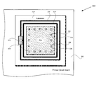
- Exemplary structure 300 illustrates a packaging approach in accordance with one embodiment of the invention.
- Exemplary structure 300 comprises packaging substrate 316 mounted onto printed circuit board (“PCB”) 340 .
- Packaging substrate 316 can be connected to PCB 340 in a manner known in the art, for example through solder balls of a ball grid array (not shown).
- packaging substrate 316 is similar to packaging substrate 216 in FIG. 2 .
- packaging substrate 316 has a voltage regulator, i.e. voltage regulator 310 , attached directly on packaging substrate 316 .
- Voltage regulator 310 is connected to input voltage ring 312 which supplies voltage regulator 310 with a 3.3 input voltage.
- Voltage regulator 310 is also connected to output voltage ring 314 .
- voltage regulator 310 takes the 3.3 input voltage from input voltage ring 312 and produces a 1.8 output voltage that is then carried by output voltage ring 314 .
- Input voltage ring 312 and output voltage ring 314 are thus equivalent to input voltage ring 212 and output voltage ring 214 , respectively, illustrated in FIG. 2 .
- the dimensions of input voltage ring 312 and output voltage ring 314 should be suitable for the current they are intended to carry and also be sufficient to support subsequent bonding wires. As an example, the width of the voltage rings can be approximately 50 microns wide.
- semiconductor die 320 is mounted and attached to packaging substrate 316 and is “encircled” by input voltage ring 312 and output voltage ring 314 .
- Semiconductor die 320 can be attached to packaging substrate 316 in a manner known in the art, such as by utilization of an epoxy.
- Semiconductor die 320 comprises bond pads, such as bond pads 326 and 330 .
- the bond pads of semiconductor die 320 generally serve as means by which semiconductor die 320 can receive Vdd and ground and also as means by which semiconductor die 320 can be electrically connected to other devices on PCB 340 by way of, for example, bond wires and/or leads in a manner known in the art.
- the bond pads providing means for electrical connection to other devices are also referred to as “signal bond pads” in the present application.
- bond pad 326 is connected to input voltage ring 312 by bond wire 328
- bond pad 330 is connected to output voltage ring 314 by bond wire 332 .
- bond pad 326 is connected to the 3.3 volt external power supply that is also supplying power to voltage regulator 310 .
- the 1.8 volts outputted from voltage regulator 310 provides power to bond pad 330 , also called the “core Vdd bond pad” in the present application.
- Core Vdd bond pad 330 can in turn supply the core circuitry of semiconductor die 320 with a steady 1.8 volts.
- Vdd bond pad 330 the appropriate Vdd level, for example 1.8 volts, can be provided to the core circuitry of semiconductor die 320 .
- Bond pad 326 also called “I/O Vdd bond pad” in the present application, provides the desired Vdd level to the respective input/output (“I/O”) circuitry associated with each signal bond pad in semiconductor die 320 .
- I/O input/output
- power to the I/O circuitry associated with each signal bond pad of semiconductor die 320 can be easily provided by utilization of bond wires and bond pads, such as bond wire 328 and I/O Vdd bond pad 326 .
- I/O Vdd bond pad 326 the appropriate Vdd level, for example 3.3 volts, can be provided to the I/O circuitry associated with each signal bond pad of semiconductor die 320 .
- I/O voltage ring 312 is also referred to as “I/O voltage ring” 312 while output voltage ring 314 is also referred to as “core voltage ring” 314 .
- I/O voltage ring 312 and core voltage ring 314 can in general be of any configuration or geometry and are not limited to a “ring” configuration. In fact, a common configuration for either ring 312 or ring 314 is a straight distribution line.
- I/O voltage ring 312 is generally referred to as an “I/O voltage line” while core voltage ring 314 is generally referred to as a “core voltage line” in the present application.
- exemplary structure 300 shown in FIG. 3 illustrates an innovative packaging approach wherein the voltage regulator is placed off-die and directly on the packaging substrate.
- the voltage regulator supplies the core circuitry of the semiconductor die with a stable and desired voltage through bond wires connecting bond pads on the semiconductor die to the voltage regulator's output voltage ring.
- the I/O circuitry of the semiconductor die are supplied with the voltage regulator's input voltage by way of bond wires to an input voltage ring which is also connected to the voltage regulator and provides the voltage regulator with an input power supply.
- two or more off-die voltage regulators are connected in series to provide the core circuitry of the semiconductor die with greater current as may be needed.
- An input voltage line can be connected to the voltage regulators, which can generate a steady output voltage to an output voltage ring encircling the semiconductor die.
- the output voltage from the off-die voltage regulators being carried by the output voltage ring can be tapped into by the semiconductor die through bond wires and bond pads.
- the present invention provides voltage regulation for semiconductor dies and related structure.
- the placement of the voltage regulator off-die results in superior voltage regulation, since the off-die voltage regulator is not exposed to the noise produced by the digital circuitry of the semiconductor die containing the core.
- Another advantage of the present invention over the conventional on-die voltage regulators is the freeing up of valuable semiconductor die space for uses related to the core functions.
- the voltage regulator in the present invention is placed off-die, the voltage regulator can be fabricated utilizing a relatively inexpensive process, such as a 0.25 micron CMOS process, to further reduce production costs, while the semiconductor die carrying the core circuitry can be fabricated by a more advanced process.
Abstract
Description
Claims (23)
Priority Applications (1)
| Application Number | Priority Date | Filing Date | Title |
|---|---|---|---|
| US09/971,162 US6674646B1 (en) | 2001-10-05 | 2001-10-05 | Voltage regulation for semiconductor dies and related structure |
Applications Claiming Priority (1)
| Application Number | Priority Date | Filing Date | Title |
|---|---|---|---|
| US09/971,162 US6674646B1 (en) | 2001-10-05 | 2001-10-05 | Voltage regulation for semiconductor dies and related structure |
Publications (1)
| Publication Number | Publication Date |
|---|---|
| US6674646B1 true US6674646B1 (en) | 2004-01-06 |
Family
ID=29737341
Family Applications (1)
| Application Number | Title | Priority Date | Filing Date |
|---|---|---|---|
| US09/971,162 Expired - Lifetime US6674646B1 (en) | 2001-10-05 | 2001-10-05 | Voltage regulation for semiconductor dies and related structure |
Country Status (1)
| Country | Link |
|---|---|
| US (1) | US6674646B1 (en) |
Cited By (6)
| Publication number | Priority date | Publication date | Assignee | Title |
|---|---|---|---|---|
| US20060131725A1 (en) * | 2004-12-17 | 2006-06-22 | Anwar Ali | System for implementing a configurable integrated circuit |
| US20070070673A1 (en) * | 2005-09-28 | 2007-03-29 | Shekhar Borkar | Power delivery and power management of many-core processors |
| US20110167629A1 (en) * | 2004-12-31 | 2011-07-14 | Stmicroelectronics Pvt. Ltd. | Area-efficient distributed device structure for integrated voltage regulators |
| CN101043033B (en) * | 2006-03-23 | 2011-12-14 | 瑞萨电子株式会社 | Semiconductor integrated circuit device |
| US20140253279A1 (en) * | 2013-03-08 | 2014-09-11 | Qualcomm Incorporated | Coupled discrete inductor with flux concentration using high permeable material |
| US11953926B2 (en) | 2022-06-16 | 2024-04-09 | Skyworks Solutions, Inc. | Voltage regulation schemes for powering multiple circuit blocks |
Citations (10)
| Publication number | Priority date | Publication date | Assignee | Title |
|---|---|---|---|---|
| US3836697A (en) * | 1971-04-21 | 1974-09-17 | Gen Electric | High current interconnection assembly in a microcircuit package |
| US5744944A (en) * | 1995-12-13 | 1998-04-28 | Sgs-Thomson Microelectronics, Inc. | Programmable bandwidth voltage regulator |
| US5757171A (en) * | 1996-12-31 | 1998-05-26 | Intel Corporation | On-board voltage regulators with automatic processor type detection |
| US5831810A (en) * | 1996-08-21 | 1998-11-03 | International Business Machines Corporation | Electronic component package with decoupling capacitors completely within die receiving cavity of substrate |
| US5939868A (en) * | 1996-03-29 | 1999-08-17 | Intel Corporation | Method and apparatus for automatically controlling integrated circuit supply voltages |
| US5938769A (en) * | 1997-04-21 | 1999-08-17 | Friendtech Computer Co., Ltd. | CPU escalating adapter with multivoltage and multiple frequency selection |
| US6116863A (en) * | 1997-05-30 | 2000-09-12 | University Of Cincinnati | Electromagnetically driven microactuated device and method of making the same |
| US6230276B1 (en) * | 1999-02-01 | 2001-05-08 | Douglas T Hayden | Energy conserving measurement system under software control and method for battery powered products |
| US6363450B1 (en) * | 1999-03-17 | 2002-03-26 | Dell Usa, L.P. | Memory riser card for a computer system |
| US6476486B1 (en) * | 1997-10-30 | 2002-11-05 | Agilent Technologies, Inc. | Ball grid array package with supplemental electronic component |
-
2001
- 2001-10-05 US US09/971,162 patent/US6674646B1/en not_active Expired - Lifetime
Patent Citations (10)
| Publication number | Priority date | Publication date | Assignee | Title |
|---|---|---|---|---|
| US3836697A (en) * | 1971-04-21 | 1974-09-17 | Gen Electric | High current interconnection assembly in a microcircuit package |
| US5744944A (en) * | 1995-12-13 | 1998-04-28 | Sgs-Thomson Microelectronics, Inc. | Programmable bandwidth voltage regulator |
| US5939868A (en) * | 1996-03-29 | 1999-08-17 | Intel Corporation | Method and apparatus for automatically controlling integrated circuit supply voltages |
| US5831810A (en) * | 1996-08-21 | 1998-11-03 | International Business Machines Corporation | Electronic component package with decoupling capacitors completely within die receiving cavity of substrate |
| US5757171A (en) * | 1996-12-31 | 1998-05-26 | Intel Corporation | On-board voltage regulators with automatic processor type detection |
| US5938769A (en) * | 1997-04-21 | 1999-08-17 | Friendtech Computer Co., Ltd. | CPU escalating adapter with multivoltage and multiple frequency selection |
| US6116863A (en) * | 1997-05-30 | 2000-09-12 | University Of Cincinnati | Electromagnetically driven microactuated device and method of making the same |
| US6476486B1 (en) * | 1997-10-30 | 2002-11-05 | Agilent Technologies, Inc. | Ball grid array package with supplemental electronic component |
| US6230276B1 (en) * | 1999-02-01 | 2001-05-08 | Douglas T Hayden | Energy conserving measurement system under software control and method for battery powered products |
| US6363450B1 (en) * | 1999-03-17 | 2002-03-26 | Dell Usa, L.P. | Memory riser card for a computer system |
Cited By (14)
| Publication number | Priority date | Publication date | Assignee | Title |
|---|---|---|---|---|
| US7075179B1 (en) * | 2004-12-17 | 2006-07-11 | Lsi Logic Corporation | System for implementing a configurable integrated circuit |
| US20060131725A1 (en) * | 2004-12-17 | 2006-06-22 | Anwar Ali | System for implementing a configurable integrated circuit |
| US8426924B2 (en) * | 2004-12-31 | 2013-04-23 | Stmicroelectronics Pvt. Ltd. | Area-efficient distributed device structure for integrated voltage regulators |
| US9018046B2 (en) * | 2004-12-31 | 2015-04-28 | Stmicroelectronics International N.V. | Area-efficient distributed device structure for integrated voltage regulators |
| US20130205587A1 (en) * | 2004-12-31 | 2013-08-15 | Stmicroelectronics Pvt. Ltd. | Area-efficient distributed device structure for integrated voltage regulators |
| US20110167629A1 (en) * | 2004-12-31 | 2011-07-14 | Stmicroelectronics Pvt. Ltd. | Area-efficient distributed device structure for integrated voltage regulators |
| US7568115B2 (en) * | 2005-09-28 | 2009-07-28 | Intel Corporation | Power delivery and power management of many-core processors |
| DE112006002506B4 (en) * | 2005-09-28 | 2012-08-16 | Intel Corporation | Energy delivery and energy management in multi-core processors |
| CN102073371B (en) * | 2005-09-28 | 2013-03-27 | 英特尔公司 | Power delivery and power management of many-core processors |
| CN101278250B (en) * | 2005-09-28 | 2011-04-13 | 英特尔公司 | Power delivery and power management of many-core processors |
| US20070070673A1 (en) * | 2005-09-28 | 2007-03-29 | Shekhar Borkar | Power delivery and power management of many-core processors |
| CN101043033B (en) * | 2006-03-23 | 2011-12-14 | 瑞萨电子株式会社 | Semiconductor integrated circuit device |
| US20140253279A1 (en) * | 2013-03-08 | 2014-09-11 | Qualcomm Incorporated | Coupled discrete inductor with flux concentration using high permeable material |
| US11953926B2 (en) | 2022-06-16 | 2024-04-09 | Skyworks Solutions, Inc. | Voltage regulation schemes for powering multiple circuit blocks |
Similar Documents
| Publication | Publication Date | Title |
|---|---|---|
| US5789809A (en) | Thermally enhanced micro-ball grid array package | |
| US7872335B2 (en) | Lead frame-BGA package with enhanced thermal performance and I/O counts | |
| US9859194B2 (en) | Semiconductor device and method for manufacturing the same | |
| US6933610B2 (en) | Method of bonding a semiconductor die without an ESD circuit and a separate ESD circuit to an external lead, and a semiconductor device made thereby | |
| US20150043181A1 (en) | Enhanced stacked microelectronic assemblies with central contacts and improved ground or power distribution | |
| US5789816A (en) | Multiple-chip integrated circuit package including a dummy chip | |
| EP2647047B1 (en) | Semiconductor device with stacked power converter | |
| US10582617B2 (en) | Method of fabricating a circuit module | |
| US7403399B2 (en) | Active primary-sided circuit arrangement for a switch-mode power supply | |
| JPH04307943A (en) | Semiconductor device | |
| US6897555B1 (en) | Integrated circuit package and method for a PBGA package having a multiplicity of staggered power ring segments for power connection to integrated circuit die | |
| US6650015B2 (en) | Cavity-down ball grid array package with semiconductor chip solder ball | |
| US6674646B1 (en) | Voltage regulation for semiconductor dies and related structure | |
| US7737541B2 (en) | Semiconductor chip package structure | |
| US6861762B1 (en) | Flip chip with novel power and ground arrangement | |
| KR100408391B1 (en) | Ball grid array package semiconductor device having improved power line routing | |
| US6495910B1 (en) | Package structure for accommodating thicker semiconductor unit | |
| US11462494B2 (en) | Semiconductor device package having galvanic isolation and method therefor | |
| JP3730644B2 (en) | Semiconductor device | |
| EP0486027B1 (en) | Resin sealed semiconductor device | |
| JP2005057126A (en) | Semiconductor device | |
| US20090294985A1 (en) | Thin chip scale semiconductor package | |
| US9543238B1 (en) | Semiconductor device | |
| US8749011B2 (en) | System and method for reducing voltage drops in integrated circuits | |
| CN116960099A (en) | Packaging structure |
Legal Events
| Date | Code | Title | Description |
|---|---|---|---|
| AS | Assignment |
Owner name: CONEXANT SYSTEMS, INC., CALIFORNIA Free format text: ASSIGNMENT OF ASSIGNORS INTEREST;ASSIGNORS:GOLSHAN, KHOSROW;FAZELPOUR, SIAMAK;HASHEMI, HASSAN S.;REEL/FRAME:012229/0661 Effective date: 20010912 |
|
| AS | Assignment |
Owner name: SKYWORKS SOLUTIONS, INC., MASSACHUSETTS Free format text: ASSIGNMENT OF ASSIGNORS INTEREST;ASSIGNOR:CONEXANT SYSTEMS, INC.;REEL/FRAME:013269/0018 Effective date: 20020625 |
|
| AS | Assignment |
Owner name: CONEXANT SYSTEMS, INC., CALIFORNIA Free format text: SECURITY INTEREST;ASSIGNOR:ALPHA INDUSTRIES, INC.;REEL/FRAME:013240/0860 Effective date: 20020625 |
|
| AS | Assignment |
Owner name: ALPHA INDUSTRIES, INC., MASSACHUSETTS Free format text: RELEASE AND RECONVEYANCE/SECURITY INTEREST;ASSIGNOR:CONEXANT SYSTEMS, INC.;REEL/FRAME:014580/0880 Effective date: 20030307 |
|
| STCF | Information on status: patent grant |
Free format text: PATENTED CASE |
|
| FPAY | Fee payment |
Year of fee payment: 4 |
|
| FEPP | Fee payment procedure |
Free format text: PAYER NUMBER DE-ASSIGNED (ORIGINAL EVENT CODE: RMPN); ENTITY STATUS OF PATENT OWNER: LARGE ENTITY Free format text: PAYOR NUMBER ASSIGNED (ORIGINAL EVENT CODE: ASPN); ENTITY STATUS OF PATENT OWNER: LARGE ENTITY |
|
| FPAY | Fee payment |
Year of fee payment: 8 |
|
| FEPP | Fee payment procedure |
Free format text: PAYER NUMBER DE-ASSIGNED (ORIGINAL EVENT CODE: RMPN); ENTITY STATUS OF PATENT OWNER: LARGE ENTITY Free format text: PAYOR NUMBER ASSIGNED (ORIGINAL EVENT CODE: ASPN); ENTITY STATUS OF PATENT OWNER: LARGE ENTITY |
|
| AS | Assignment |
Owner name: SNAPTRACK, INC., CALIFORNIA Free format text: ASSIGNMENT OF ASSIGNORS INTEREST;ASSIGNOR:SKYWORKS SOLUTIONS, INC.;REEL/FRAME:033326/0359 Effective date: 20140707 |
|
| FPAY | Fee payment |
Year of fee payment: 12 |