US6734906B1 - Image pickup apparatus with photoelectric conversion portions arranged two dimensionally - Google Patents
Image pickup apparatus with photoelectric conversion portions arranged two dimensionally Download PDFInfo
- Publication number
- US6734906B1 US6734906B1 US09/386,345 US38634599A US6734906B1 US 6734906 B1 US6734906 B1 US 6734906B1 US 38634599 A US38634599 A US 38634599A US 6734906 B1 US6734906 B1 US 6734906B1
- Authority
- US
- United States
- Prior art keywords
- signal
- photoelectric conversion
- circuit
- noise
- common
- Prior art date
- Legal status (The legal status is an assumption and is not a legal conclusion. Google has not performed a legal analysis and makes no representation as to the accuracy of the status listed.)
- Expired - Lifetime
Links
- 238000006243 chemical reaction Methods 0.000 title claims abstract description 100
- 238000012545 processing Methods 0.000 claims description 11
- 239000003990 capacitor Substances 0.000 description 103
- 238000010586 diagram Methods 0.000 description 38
- 238000012546 transfer Methods 0.000 description 37
- 230000008030 elimination Effects 0.000 description 21
- 238000003379 elimination reaction Methods 0.000 description 21
- 230000003321 amplification Effects 0.000 description 20
- 238000003199 nucleic acid amplification method Methods 0.000 description 20
- 101000588067 Homo sapiens Metaxin-1 Proteins 0.000 description 12
- 102100031603 Metaxin-1 Human genes 0.000 description 12
- 230000005484 gravity Effects 0.000 description 8
- 238000000034 method Methods 0.000 description 8
- 101000727837 Rattus norvegicus Reduced folate transporter Proteins 0.000 description 6
- 238000009825 accumulation Methods 0.000 description 3
- 238000005286 illumination Methods 0.000 description 3
- 230000006835 compression Effects 0.000 description 2
- 238000007906 compression Methods 0.000 description 2
- 230000007547 defect Effects 0.000 description 2
- 239000011159 matrix material Substances 0.000 description 2
- 229910052751 metal Inorganic materials 0.000 description 2
- 239000002184 metal Substances 0.000 description 2
- 230000003287 optical effect Effects 0.000 description 2
- 230000002093 peripheral effect Effects 0.000 description 2
- 230000035945 sensitivity Effects 0.000 description 2
- 238000013519 translation Methods 0.000 description 2
- 239000003086 colorant Substances 0.000 description 1
- 239000013065 commercial product Substances 0.000 description 1
- 239000004020 conductor Substances 0.000 description 1
- 239000013078 crystal Substances 0.000 description 1
- AMGQUBHHOARCQH-UHFFFAOYSA-N indium;oxotin Chemical compound [In].[Sn]=O AMGQUBHHOARCQH-UHFFFAOYSA-N 0.000 description 1
- 238000000059 patterning Methods 0.000 description 1
- 230000003252 repetitive effect Effects 0.000 description 1
- 238000005070 sampling Methods 0.000 description 1
- 239000000758 substrate Substances 0.000 description 1
- 230000002195 synergetic effect Effects 0.000 description 1
Images


Classifications
-
- H—ELECTRICITY
- H01—ELECTRIC ELEMENTS
- H01L—SEMICONDUCTOR DEVICES NOT COVERED BY CLASS H10
- H01L27/00—Devices consisting of a plurality of semiconductor or other solid-state components formed in or on a common substrate
- H01L27/14—Devices consisting of a plurality of semiconductor or other solid-state components formed in or on a common substrate including semiconductor components sensitive to infrared radiation, light, electromagnetic radiation of shorter wavelength or corpuscular radiation and specially adapted either for the conversion of the energy of such radiation into electrical energy or for the control of electrical energy by such radiation
- H01L27/144—Devices controlled by radiation
- H01L27/146—Imager structures
- H01L27/14601—Structural or functional details thereof
- H01L27/14641—Electronic components shared by two or more pixel-elements, e.g. one amplifier shared by two pixel elements
-
- H—ELECTRICITY
- H04—ELECTRIC COMMUNICATION TECHNIQUE
- H04N—PICTORIAL COMMUNICATION, e.g. TELEVISION
- H04N25/00—Circuitry of solid-state image sensors [SSIS]; Control thereof
- H04N25/60—Noise processing, e.g. detecting, correcting, reducing or removing noise
- H04N25/616—Noise processing, e.g. detecting, correcting, reducing or removing noise involving a correlated sampling function, e.g. correlated double sampling [CDS] or triple sampling
-
- H—ELECTRICITY
- H04—ELECTRIC COMMUNICATION TECHNIQUE
- H04N—PICTORIAL COMMUNICATION, e.g. TELEVISION
- H04N25/00—Circuitry of solid-state image sensors [SSIS]; Control thereof
- H04N25/70—SSIS architectures; Circuits associated therewith
- H04N25/71—Charge-coupled device [CCD] sensors; Charge-transfer registers specially adapted for CCD sensors
- H04N25/75—Circuitry for providing, modifying or processing image signals from the pixel array
-
- H—ELECTRICITY
- H04—ELECTRIC COMMUNICATION TECHNIQUE
- H04N—PICTORIAL COMMUNICATION, e.g. TELEVISION
- H04N25/00—Circuitry of solid-state image sensors [SSIS]; Control thereof
- H04N25/70—SSIS architectures; Circuits associated therewith
- H04N25/76—Addressed sensors, e.g. MOS or CMOS sensors
- H04N25/77—Pixel circuitry, e.g. memories, A/D converters, pixel amplifiers, shared circuits or shared components
- H04N25/778—Pixel circuitry, e.g. memories, A/D converters, pixel amplifiers, shared circuits or shared components comprising amplifiers shared between a plurality of pixels, i.e. at least one part of the amplifier must be on the sensor array itself
Definitions
- the present invention relates to an image pickup apparatus for detecting image information of an object, and an image pickup system using the image pickup apparatus.
- a CMOS area sensor is one of amplification type sensors, which has a CMOS amplification circuit in each pixel.
- the CMOS area sensor is superior to a CCD type area sensor, in terms of random access, a variety of functions and a small power consumption.
- a CCD type area sensor has a large power consumption, and photoelectrically converted signals are sequentially transferred to the output circuit so that random access is difficult.
- a CMOS area sensor can output an image signal by selecting a desired pixel, so that it has a low power consumption and low noises and is easy to be fabricated.
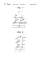
- FIGS. 1 to 3 are schematic circuit diagrams showing examples of a conventional variation compensation circuit of an image pickup apparatus.
- the structure shown in FIG. 2 is disclosed in JP-A-1-245769, and the structure shown in FIG. 3 is disclosed in JP-A-9-247546.
- a capacitor CS and a capacitor CN for storing a signal and a noise of each pixel are connected via transistors MS and MN to a vertical output line to which the output terminals of a plurality of pixels are connected.
- a signal and noise stored in the capacitors CS and CN are transferred to a horizontal output line when transistors MC 1 and MC 2 are turned on by a horizontal shift register (H•SR), and the noise is removed from the signal by a subtraction amplifier.
- H•SR horizontal shift register
- the noise is subtracted from the signal by reset means MP 1 and MP 2 connected to the electrodes of capacitors Cp and Cp, and a noise removed signal is temporarily stored in a capacitor CS.
- the noise is output to the input electrode side of the capacitor Cp, and after the output electrode side of the capacitor Cp is made in a floating state, the signal is input to the input electrode side of the capacitor Cp. Since the input electrode side of the capacitor Cp changes its potential by a (signal ⁇ noise) potential and similarly the output electrode side of the capacitor Cp changes its potential by a (signal ⁇ noise) potential, a signal with the noise removed can be output.
- a signal stored in the capacitor CS is transferred to the horizontal output line when the transistor MC is turned on by a horizontal shift register (H•SR).
- the noise read from the vertical output line is subtracted from the signal read from the vertical output line and the noise removed signal is temporarily stored in the capacitor CS.
- transistors Mt and Mr are turned on and reset, and thereafter during a noise output period, a negative pulse is applied to the capacitor Cp to transfer the charges over the channel potential ⁇ n of the transistor MS to the capacitor CS, which charges are drained by turning on the transistor Mt.
- a negative pulse is applied to the capacitor Cp to transfer the charges over the channel potential ⁇ s of the transistor MS to the capacitor CS.
- the charges transferred to the capacitor CS are Cp ⁇ ( ⁇ s ⁇ n) which correspond to the noise removed signal.
- two capacitors are provided at the minimum at one pixel line (one vertical output line).
- the capacitance of a capacitor is determined by the thickness of a dielectric layer and the electrode area.
- the capacitors generally occupy several tens % of the chip area.
- an amplifier for subtracting the noise from the signal is required for each pixel and the power consumption becomes large. If signals of a plurality of horizontal lines are read at the same time in order to lower a read speed, the temporary storage capacitor is required to have a large capacitance, resulting in a large chip area. In the image pickup apparatus shown in FIG. 2, even if the capacitor CS is omitted and the signal and noise are output to the horizontal output line without being temporarily stored, a circuit for subtracting the noise is required for each line, resulting in a large chip area.
- a recent digital still camera has several million pixels and an increased consumption power.
- the number of images capable of being stored therefore reduces and a user is requested to incur a high battery cost.
- an image pickup apparatus comprising unit cells arranged in a plurality of lines, each unit cell including a plurality of photoelectric conversion portions arranged at least in a horizontal direction and a common circuit to which signals from the plurality of photoelectric conversion portions are input; and subtracting means shared by respective photoelectric conversion portions of at least one of the unit cells.
- an image pickup apparatus comprising: a plurality of photoelectric conversion pixels; and subtracting means shared by at least two photoelectric conversion pixels adjacent in the plurality of photoelectric conversion pixels.
- an image pickup apparatus comprising: unit cells arranged in a plurality of lines, each including a plurality of photoelectric conversion portions disposed at least in a horizontal direction and a common circuit to which signals from the plurality of photoelectric conversion portions are input; and signal holding means shared by respective photoelectric conversion portions of at least one of the unit cells.
- an image pickup apparatus comprising: a plurality of photoelectric conversion pixels; and signal holding means shared by at least two photoelectric conversion pixels adjacent in the plurality of photoelectric conversion pixels, wherein the signal holding means stores in parallel first and second signals generated in the photoelectric conversion pixel.
- FIG. 1 is a schematic circuit diagram showing an example of a noise eliminating circuit of a conventional image pickup apparatus.
- FIG. 2 is a schematic circuit diagram showing another example of a noise eliminating circuit of a conventional image pickup apparatus.
- FIG. 3 is a schematic circuit diagram showing another example of a noise eliminating circuit of a conventional image pickup apparatus.
- FIG. 4 is a schematic circuit diagram showing the structure of an image pickup apparatus according to a first embodiment of the invention.
- FIG. 5 is a diagram showing the structure of a photoelectric conversion pixel.
- FIG. 6 is a timing chart illustrating the operation of the image pickup apparatus shown in FIG. 5 .
- FIG. 7 is a schematic circuit diagram showing the structure of an image pickup apparatus according to a second embodiment of the invention.
- FIG. 8 is a timing chart illustrating the operation of the image pickup apparatus shown in FIG. 7 .
- FIG. 9 is a schematic circuit diagram showing the structure of an image pickup apparatus according to a third embodiment of the invention.
- FIG. 10 is a diagram showing the structure of a unit cell.
- FIG. 11 is a schematic circuit diagram showing the structure of an image pickup apparatus according to a fourth embodiment of the invention.
- FIG. 12 is a schematic circuit diagram showing the structure of an image pickup apparatus according to a fifth embodiment of the invention.
- FIG. 13 is a schematic circuit diagram showing the structure of an image pickup apparatus according to a sixth embodiment of the invention.
- FIG. 14 is a diagram showing the overall structure of the image pickup apparatus.
- FIG. 15 is a schematic circuit diagram showing the structure of an image pickup apparatus according to a seventh embodiment of the invention.
- FIG. 16 is a timing chart illustrating the operation of the image pickup apparatus shown in FIG. 15 .
- FIG. 17 is a timing chart illustrating the operation during each color signal read period.
- FIG. 18 is a diagram showing the overall structure of the image pickup apparatus shown in FIG. 15 .
- FIG. 19 is a schematic circuit diagram showing the structure of an image pickup apparatus according to an eighth embodiment of the invention.
- FIG. 20 is a schematic block diagram showing the outline of a system according to a ninth embodiment of the invention.
- FIG. 21 is a diagram showing a layout of a unit cell according to a tenth embodiment of the invention.
- FIG. 22 is a diagram showing another layout of a unit cell according to the tenth embodiment of the invention.
- FIG. 23 is a diagram showing an example of a pattern layout according to the tenth embodiment of the invention.
- FIG. 24 is a diagram showing another example of a pattern layout according to the tenth embodiment of the invention.
- FIG. 25 is a diagram showing an example of the structure of a unit cell according to the tenth embodiment of the invention.
- FIG. 26 is a diagram showing another example of a pattern layout according to the tenth embodiment of the invention.
- FIG. 27 is a diagram showing another example of the structure of a unit cell according to the tenth embodiment of the invention.
- FIG. 28 is a diagram showing an example of a layout of a unit cell of an image pickup apparatus.
- FIG. 4 is a schematic circuit diagram showing the structure of an image pickup apparatus according to the first embodiment of the invention.
- FIG. 5 is a circuit diagram of a photoelectric conversion pixel. The fundamental structure of the noise eliminating circuit is the same as that shown in FIG. 2 .
- photoelectric conversion pixels a and c are connected to a vertical output line VL 1
- photoelectric conversion pixels b and d are connected to a vertical output line VL 2
- the vertical output line VL 1 is connected via a transistor M 1 to a noise eliminating capacitor Cp
- the vertical output line VL 2 is connected via a transistor M 2 to the noise eliminating capacitor Cp.
- the input side of the capacitor Cp is connected to a transistor M 3
- the output side thereof is connected to a transistor M 4 so that the input and output electrodes of the capacitor Cp can be set to predetermined potentials.
- the noise of the pixel a is output to the input electrode side of the capacitor Cp by turning the transistor M 1 on, and after the output electrode side of the capacitor Cp is made in a floating state, the signal of the pixel a is input to the input electrode side of the capacitor Cp. Since the input electrode side of the capacitor Cp changes its potential by a (signal ⁇ noise) potential and similarly the output electrode side of the capacitor Cp changes its potential by a (signal ⁇ noise) potential, a signal with the noise removed can be output. In a similar manner, the noise of the pixel b is removed from the signal.
- the noise removed signal of the pixel a can be stored in a capacitor Ca by turning on a transistor M 5
- a noise removed signal of the pixel b can be stored in a capacitor Cb by turning on a transistor M 6 .
- H•SR horizontal shift register
- the noise removed signal of the pixel a and the noise removed signal of the pixel b can be output to the horizontal output line.
- Reference numeral 100 represents a noise elimination/signal storage unit.
- FIG. 5 is a circuit diagram of a photoelectric conversion pixel.
- the photoelectric conversion pixel includes: a photodiode PD as a photoelectric conversion portion, a transfer means MTX for transferring a signal charge from the photodiode PD; an amplification means MSF for amplifying and outputting the transferred signal charge; a reset means MRES for resetting the pixel, and a select means MSEL for selecting the pixel.
- the transfer means MTX is turned on by a control signal ⁇ GT when the signal from the photodiode PD is transferred to an input portion (gate) of the amplification means MSF.
- the select means MSEL is turned on by a select signal ⁇ SO when a signal corresponding to the signal charge transferred to the gate of the amplification means MSF is read to the vertical output line.
- the reset means MRES is turned on by the reset signal ⁇ GCL so that the input portion of the amplification means MSF is reset and the noise is sent via the select means MSEL to the vertical output line.
- FIG. 6 is a timing chart illustrating the operation of the image pickup apparatus.
- signals ⁇ VL and ⁇ M 1 are set to a high level to turn on the transistors M 3 and M 1 and remove residual charges on the vertical output line VL 1 .
- signals ⁇ GCK, ⁇ SO, ⁇ HCL, ⁇ T 1 and ⁇ M 1 are set to the high level, so that the reset means MRES of the pixel a is turned on and the common amplifier is reset, and that the select means MSEL and transistor M 1 are turned on to read the noise of the common amplifier and transfer the noise to the input electrode of the capacitor Cp while the output electrode of the capacitor Cp is maintained at a constant potential.
- the capacitor Ca is also reset to a constant potential.
- ⁇ HCL is set to a low level so that the output electrode of the capacitor Cp is made in a floating state.
- signals ⁇ GT, ⁇ SO, ⁇ T 1 and ⁇ M 1 are set to the high level, so that the transfer means MTX is turned on to transfer the signal in the photoelectric conversion portion of the pixel a to the input portion (gate) of the common amplifier, and that the select means MSEL and transistors M 1 and M 5 are turned on to read the photoelectric conversion signal, transfer it to the input electrode of the capacitor Cp, and store the noise removed photoelectric conversion signal in the capacitor Ca.
- the noise elimination operation is performed in the manner described earlier.
- the signal of the pixel b is read in the manner similar to the signal read of the pixel a.
- the photoelectric conversion signals of the pixels a and b stored in the capacitors Ca and Cb are sequentially read by the horizontal shift resister (H•SR).
- the capacitors Ca and Cb are provided at the output side of the capacitor Cp to temporarily store the signals of the pixels a and b.
- the capacitors Ca and Cb may be omitted to sequentially output the signals from the pixels to the horizontal output line without temporarily storing the signals.
- FIG. 7 is a schematic circuit diagram showing the structure of an image pickup apparatus according to the second embodiment of the invention.
- the noise eliminating circuit is different from the structure shown in FIG. 4 .
- the fundamental structure of the noise eliminating circuit is the same as that shown in FIG. 3 .
- Reference numeral 200 represents a noise elimination/signal storage unit.
- vertical output lines VL 1 and VL 2 are connected to the gate of a common transistor M 9 via transistors M 1 and M 2 .
- the drain of the common transistor M 9 is connected to a capacitor Cp and a transistor M 11 , and the source thereof is connected to a transistor M 10 and via transistors M 5 and M 6 to capacitors Ca and Cb.
- transistors M 11 , M 10 and M 5 are turned on and reset, and thereafter during a noise output period of the pixel a, a negative pulse is applied to the capacitor Cp to transfer the charges over the channel potential ⁇ n of the transistor M 9 to the capacitor Ca, which charges are drained by turning on the transistor M 10 .
- a negative pulse is applied to the capacitor Cp to transfer the charges over the channel potential ⁇ s of the transistor M 9 to the capacitor Ca.
- the charges transferred to the capacitor Ca are Cp ⁇ ( ⁇ s ⁇ n) which correspond to the noise removed signal.
- the noise removed signal of the pixel b is stored in the capacitor Cb. Thereafter, similar to the first embodiment, the noise removed signal of the pixel a and the noise removed signal of the pixel b are sequentially output to the horizontal output line.
- FIG. 8 is a timing chart illustrating the operation of the image pickup apparatus.
- the signal of the pixel a is read.
- the signals ⁇ VL and ⁇ M 1 are set to the high level to turn on the transistors M 3 and M 1 and remove residual charges on the vertical output line VL 1 .
- signals ⁇ HCL, ⁇ CL and ⁇ T 1 are set to the high level to turn on the transistors M 10 , M 11 and M 5 and reset the residual charges.
- signals ⁇ HCL, ⁇ SO and ⁇ M 1 are set to the high level, so that the reset means MRES of the pixel a is turned on and the common amplifier is reset, and that the select means MSEL and transistor M 1 are turned on to read the noise of the common amplifier and transfer the noise to the gate of the transistor M 9 .
- the signal ⁇ T 1 is set to the high level
- the signal ⁇ CP is set to the low level
- a negative pulse is applied to the capacitor Cp to transfer charges over the channel potential ⁇ n of the transistor M 9 to the capacitor Ca.
- signals ⁇ HCL and ⁇ T 1 are set to the high level to turn on the transistors M 10 , M 11 and M 5 and drain the charge in the capacitor Ca.
- signals ⁇ HCL, ⁇ SO and ⁇ M 1 are set to the high level, so that the transfer means MTX is turned on to transfer the signal of the photoelectric conversion portion of the pixel a to the input portion (gate) of the common amplifier, and that the select means MSEL and transistor M 1 are turned on to read the photoelectric conversion signal and transfer it to the gate of the transistor M 9 .
- the signal ⁇ T 1 is set to the high level
- the signal ⁇ CP is set to the low level
- a negative pulse is again applied to the capacitor Cp to transfer charges over the channel potential ⁇ s of the transistor M 9 to the capacitor Ca.
- the charges transferred to the capacitor Ca correspond to Cp ⁇ ( ⁇ s ⁇ n) so that the noise removed signal is stored in the capacitor Ca.
- the signal of the pixel b is read in the manner similar to the signal read of the pixel a.
- the photoelectric conversion signals of the pixels a and b stored in the capacitors Ca and Cb are sequentially read by the horizontal shift resister (H•SR).
- FIG. 9 is a schematic circuit diagram showing the structure of an image pickup apparatus according to the third embodiment of the invention.
- the structure of the photoelectric conversion pixel is different from that shown in FIG. 4 .
- the structure of the noise elimination/signal storage unit is the same as the noise elimination/signal storage unit 100 shown in FIG. 4 .
- like elements to those shown in FIG. 4 are represented by using identical alphanumeric symbols and the description thereof is omitted.
- signals from four photoelectric conversion portions are output via one common amplifier.
- signals of two pixel lines (a pixel line of the photoelectric conversion portions a and c, and a pixel line of the photoelectric conversion portions b and d) can be output from one vertical output line.
- a, b, c and d represent the photoelectric conversion portions
- a 1 represents the common amplifier.
- a unit cell is constituted of the photoelectric conversion portions (e.g., photodiodes) a, b, c and d and the common amplifier A 1 , and each pixel is constituted by one photoelectric conversion portion and a portion of the common amplifier.
- FIG. 10 shows the structure of a unit cell.
- the unit cell has four photoelectric conversion portions (in this case, a 11 , a 12 , a 21 , a 22 ) per one common amplifier.
- the other unit cells have the same structure.
- the common amplifier is constituted of an amplification means MSF, a reset means MRES, a select means MSEL and transfer means MTX 1 to MTX 4 .
- the transfer means MTX 1 to MTX 4 are sequentially turned on by control signals ⁇ GT 1 to ⁇ GT 4 to sequentially transfer signals of the photoelectric conversion portions a 11 , a 12 , a 21 and a 22 to the input portion (gate) of the amplification means MSF.
- the select means MSEL When the select means MSEL is turned on by a select signal ⁇ SO, a signal corresponding to the signal charges transferred to the gate of the amplification means MSF is read to the vertical output line.
- the reset means MRES Before the signal of the photoelectric conversion portion is transferred to the input portion (gate) of the amplification means MSF, the reset means MRES is turned on by the reset signal ⁇ GCL so that the input portion of the amplification means MSF is reset and the noise is output via the select means MSEL to the vertical output line.
- FIG. 11 is a schematic circuit diagram showing the structure of an image pickup apparatus according to the fourth embodiment of the invention.
- the structure of the photoelectric conversion pixel is the same as that shown in FIG. 9, and the structure of the noise elimination/signal storage unit is the same as the noise elimination/signal storage unit 200 shown in FIG. 7 .
- FIG. 11 like elements to those shown in FIGS. 7 and 9 are represented by using identical alphanumeric symbols and the description thereof is omitted.
- FIG. 12 is a schematic circuit diagram showing the structure of an image pickup apparatus according to the fifth embodiment of the invention.
- the fundamental structure is the same as that shown in FIG. 9, a different point is the provision of signal charge capacitors Ca to Cd for the photoelectric conversion portions a to d, transistors M 12 to M 15 , and transistors M 16 to M 19 .
- a capacitor is provided for each of the photoelectric conversion portions a to d, four noise elimination capacitors Cp and four signal storage capacitors C, eight capacitors in total, are required.
- FIG. 13 is a schematic circuit diagram showing the structure of an image pickup apparatus according to the sixth embodiment of the invention.
- the fundamental structure of the noise elimination/signal storage unit 400 is the same as the noise elimination/signal storage unit 300 shown in FIG. 12, a different point is the provision of signal storage capacitors and transistors for photoelectric conversion portions a′ to d′ in addition to the photoelectric conversion portions a to d.
- the noise elimination capacitor Cp is used in common.
- the noises and signals of a unit cell line having the photoelectric conversion portions a′ to d′ in addition to a unit cell line having the photoelectric conversion portions a to d are input to the noise elimination/signal storage unit 300 .
- a capacitor is provided for each of the photoelectric conversion portions a to d and a′ to d′, eight noise elimination capacitors Cp and eight noise removed signal storage capacitors C, sixteen capacitors in total, are required. In this embodiment, it is sufficient if one noise elimination capacitor Cp and eight noise reduced signal storage capacitors C, nine capacitors in total, are provided.
- FIG. 14 is a block diagram showing the overall structure of the image pickup apparats.
- Reset, noise/signal read, and photoelectric conversion control for each photoelectric conversion cell is performed by a vertical shift register (V•SR) 15 .
- Control of the noise elimination/signal storage unit 14 such as shown at 100 , 200 and 300 in the above embodiments is performed by a horizontal shift register (H•SR) 13 .
- a signal is amplified by an amplifier 10 and converted into a digital signal via an AGC circuit 11 and an A/D converter 12 .
- a timing generator 16 is used for controlling the operation of the vertical shift register (V.SR) 15 , horizontal shift register (H•SR) 13 , amplifier 10 , AGC circuit 11 and A/D converter 12 .
- Reference numeral 17 represents an image pickup element array having photoelectric conversion cells disposed in a matrix shape.
- the unit cell may be constituted of any plurality of pixels of any plurality of lines.
- subtracting means is shared so that the number of signal storage means for storing subtraction outputs from the subtracting means can be reduced.
- JP-A-4-281683 discloses that outputs of odd and even line pixels connected to one vertical output line are supplied to a common noise elimination circuit (CDS circuit: correlation double sampling circuit), and after noises are removed, the signals from two pixels are stored in two capacitors.
- the noise elimination circuit is shared by a plurality of pixels connected to one vertical output line.
- a common subtracting means (corresponding to the noise elimination circuit) is used by the image pickup apparatus having a plurality lines of unit cells each constituted of a plurality of photoelectric conversion portions and a common amplifier, and also the common subtracting means is shared by a plurality of output lines. Therefore, this prior art has different technical concept from the present invention.
- FIG. 15 is a schematic circuit diagram showing the structure of an image pickup apparatus according to the seventh embodiment of the invention.
- a photoelectric conversion cell (unit cell) is constituted of four photoelectric conversion portions and one common amplifier.
- the photoelectric conversion portions a 11 , a 12 , a 21 and a 22 have color filters R 1 (red), G 1 (green), G 2 (green) and B 2 (blue), respectively.
- R 1 , G 1 , G 2 and B 2 signals of the photoelectric conversion portions are output via the common amplifier A 1 to the vertical output line.
- the noise signal after resetting is also output via the common amplifier A 1 to the vertical output line.
- Reference numeral 100 represents a signal storage unit constituted of a signal storage capacitor CS, a noise storage capacitor CN, capacitor switching transistors M 1 and M 2 and signal output transistors M 3 and M 4 .
- the signal storage capacitor CS and noise storage capacitor CN are connected in parallel via the transistors M 1 and M 2 to one vertical output line.
- the signal stored in the capacitor CS and the noise stored in the capacitor CN are read to respective horizontal output lines when the transistors M 3 and M 4 are turned on at the same time by the horizontal shift register (H•SR), and supplied to a subtracting amplifier 10 which subtracts the noise from the signal.
- the noise removed signal is converted into a digital signal via an AGC circuit 11 and an A/D converter 12 .
- the horizontal output lines are reset by a transistor M 6 which is controlled by ⁇ HC.
- FIG. 10 shows the structure of a photoelectric conversion cell S.
- the photoelectric conversion cell S has four photoelectric conversion portions (in this case, a 11 , a 12 , a 21 , a 22 ) per one common amplifier.
- the other photoelectric conversion cells have the same structure.
- the common amplifier is constituted of an amplification means MSF, a reset means MRES, a select means MSEL and transfer means MTX 1 to MTX 4 .
- the transfer means MTX 1 to MTX 4 are sequentially turned on by control signals ⁇ GT 1 to ⁇ GT 4 to sequentially transfer signals of the photoelectric conversion portions a 11 , a 12 , a 21 and a 22 to the input portion (gate) of the amplification means MSF.
- the select means MSEL When the select means MSEL is turned on by a select signal ⁇ SO, a signal corresponding to the signal charges transferred to the gate of the amplification means MSF is read to the vertical output line.
- the reset means MRES Before the signal of the photoelectric conversion portion is transferred to the input portion (gate) of the amplification means MSF, the reset means MRES is turned on by the reset signal ⁇ GCL so that the input portion of the amplification means MSF is reset and the noise is output via the select means MSEL to the vertical output line.
- FIG. 16 is a timing chart illustrating the operation of the image pickup apparatus shown in FIG. 15 .
- each color signal is sequentially and time divisionally read (R 1 read ( ⁇ R period) ⁇ G 1 read ( ⁇ G period) ⁇ B 2 read ( ⁇ B period) ⁇ G 2 read ( ⁇ G′ period)).
- R 1 read ⁇ R period
- G 1 read ⁇ G period
- B 2 read ⁇ B period
- G′ period ⁇ G 2 read
- the subtraction amplifier 10 subtracts the noise from the signal, and the noise removed signal is converted into a digital signal via the AGC circuit 11 and A/D converter 12 to thus output R 1 , G 1 , B 1 and G 2 digital color signals (signal out 1 ).
- an output signal is a line sequential color signal.
- the digital signals after A/D conversion are temporarily stored in a later stage storage unit and subjected to image processing.
- a noise elimination method is not limited to the embodiment method, but other methods can be applied such as a slice type illustrated in FIG. 3 .
- FIG. 17 is a timing chart illustrating the operation of the image pickup apparatus during a color signal read period.
- signals ⁇ TS, ⁇ TN and ⁇ VL are set to the high level to turn on the transistors M 1 , M 2 and M 5 and drain residual charges on the vertical output line and in the temporary storage capacitors CS and CN.
- signals ⁇ GCL, ⁇ SO and ⁇ TN are set to the high level so that the reset means MRES is turned on to reset the common amplifier and the select means MSEL and transistor M 2 are turned on to read the noise from the common amplifier and store it in the temporary storage capacitor CN.
- signals ⁇ GT, ⁇ SO and ⁇ TS are set to the high level so that the transfer means MTX 1 is turned on to transfer the signal from the photoelectric conversion portion to the input portion (gate) of the common amplifier and the select means MSEL and transistor M 1 are turned on to read the signal from the common amplifier and store it in the temporary storage capacitor CS. Similar operations are performed also for the G 1 , B 2 and G 2 read periods.
- FIG. 18 is a block diagram showing the overall structure of the image pickup apparats.
- Reset, noise/signal read, and photoelectric conversion control for each photoelectric conversion cell is performed by a vertical shift register (V•SR) 15 .
- Control of the noise elimination/signal storage unit 14 such as shown at 100 in FIG. 15 is performed by a horizontal shift register (H•SR) 13 .
- a subtraction amplifier 10 subtracts the noise from the signal, and the noise removed signal is converted into a digital signal via an AGC circuit 11 and an A/D converter 12 .
- a timing generator 16 is used for controlling the operation of the vertical shift register (V•SR) 15 , horizontal shift register (H•SR) 13 , amplifier 10 , AGC circuit 11 and A/D converter 12 .
- Reference numeral 17 represents an image pickup element array having photoelectric conversion cells disposed in a matrix shape.
- the unit cell may be constituted of any plurality of pixels of any plurality of lines.
- the common circuit A 1 , A 2 , . . . is an amplifier.
- the common circuit may be other signal processing circuits such as an A/D converter circuit and a compression circuit.
- FIG. 19 is a schematic circuit diagram showing the structure of an image pickup apparatus according to the eighth embodiment of the invention. The cell structure thereof is shown in FIG. 5 .
- control lines are provided to each of odd and even lines to control the transfer means MTX by signals ⁇ GT 1 and ⁇ GT 2 .
- Transistors M 7 and M 2 are turned on to store a noise read from a pixel R 1 in a capacitor CN, and transistors M 7 and M 1 are turned on to store a signal read from the pixel R 1 in a capacitor CS.
- the signal and noise are output from the capacitors CS and CN to horizontal output lines.
- noises and signals read from the other pixels G 1 , G 2 and B 2 are stored in the capacitors CN and CS and output to the horizontal signal lines.
- the noise storage capacitor is not necessary.
- a common control line may be used instead of discrete odd and even line control lines for the transfer means MTX.
- the image signal is transferred to the vertical output line in response to ⁇ GT and temporarily stored. Transfer of this signal to the signal storage capacitor CS is controlled by ⁇ VT 1 and ⁇ VT 2 .
- the seventh and eighth embodiments it is possible to reduce the number of temporary storage capacitors. By reducing the number of stages of a shift register, common circuits, AGCs, and A/D converters, the chip size and cost can be reduced.
- a divisional drive reduces the number of temporary storage units so that the number of transfer switches to be connected to a horizontal output line can also be reduced. Accordingly, a read gain from the temporary storage unit to the horizontal output line can be increased or conversely the capacity of a temporary storage unit can be reduced.
- the noise components are subtracted from an image signal containing the noise components to obtain an image signal with a high S/N ratio.
- an image signal obtained through light signal accumulation under illumination light such as LED illumination may be subtracted by an image signal obtained through light signal accumulation without illumination light.
- an image made of only reflection light from LED subtracted by the noise components and background object components can be obtained.
- FIG. 20 is a schematic circuit diagram showing the structure of an image pickup apparatus according to the ninth embodiment of the invention.
- the ninth embodiment shown in FIG. 20 is an image pickup system using the image pickup apparatus of any one of the first to eighth embodiments described above.
- light of an object passed through an optical system 71 and an iris 80 is focussed upon a CMOS sensor 72 .
- Light is converted by a pixel array disposed on the CMOS sensor 72 into electric signals which are then output after noises are removed.
- This output signal is supplied to a signal processing circuit 73 which performs a color process or the like.
- the processed signal is recorded or transferred by a record/transfer system 74 .
- the recorded or transferred signal is reproduced by a reproducing system 77 .
- the iris 80 , CMOS sensor 72 and signal processing circuit 73 are controlled by a timing control circuit 75 .
- the optical system 71 , timing control circuit 75 , record/transfer system 74 and reproducing system 77 are controlled by a system control circuit 76 .
- the layout of pixels shown in FIG. 28 is associated with the following problem, because of an unequal pitch (a 1 is not equal to a 2 ) of the layout of photoelectric conversion portions 173 , and hence because of an unequal pitch between adjacent light sensing areas of pixels.
- the layout of same colors with an unequal pitch results in defects such as a lowered resolution and a moire stripe, since a spatial frequency and a resolution are locally different.
- a moire stripe poses a critical issue.
- An image pickup apparatus having such defects cannot be any more a commercial product.
- a unit cell having five or more pixels is also associated with the same problem.
- an image pickup apparatus using a CMOS sensor having amplification means distributed into a plurality of pixels can have a good quality such as an improved opening area without a lowered resolution and a moire stripe, by setting an equal pitch of photoelectric conversion portions and hence an equal distance between adjacent light sensing areas.
- Such an image pickup apparatus can be properly applied to this invention.
- FIG. 21 shows an layout wherein pixels of two row and two columns share a common amplifier 22 .
- the common amplifier 22 is disposed at the center of the four pixels, four photoelectric conversion portions (A 11 , A 12 , a 21 and a 22 ) surrounding the common amplifier 22 .
- the common amplifier 22 includes the amplification means MSF, reset means MRES, select means MSEL, and transfer means MTX 1 to MTX 4 , respectively shown in FIG. 5 .
- a light shielding area 25 is disposed opposite to a partial area of the common amplifier 22 in each pixel area, symmetrical to the center of each pixel area. Therefore, the gravity center of the photoelectric conversion portion of each pixel is at the center of each pixel.
- the four photoelectric conversion portions (a 11 to a 22 ) are therefore disposed at an equal pitch a both in the vertical and horizontal directions.
- a common amplifier 32 is disposed in a central area of the unit cell in the horizontal direction between the upper and lower four pixels.
- Four photoelectric conversion portions 31 (a 11 , a 12 , a 21 and a 22 ) sandwich the common amplifier 32 .
- a light shielding area 35 is disposed opposite to a partial area of the common amplifier 32 in each pixel area, symmetrical to the center of each pixel area. Therefore, the gravity center of the photoelectric conversion portion 31 of each pixel is at the center of each pixel.
- the four photoelectric conversion portions (a 11 to a 22 ) are therefore disposed at an equal pitch a both in the vertical and horizontal directions.
- the components in the layout shown in FIG. 22 may be reversed between the vertical and horizonal directions.
- FIG. 23 shows an example of a layout of patterns of a pixel array of a CMOS sensor.
- the CMOS sensor shown in FIG. 23 is formed on a single crystal substrate by using a 0.4 ⁇ m rule.
- the size of each pixel is 8 ⁇ m square.
- a common amplifier made of a source follower amplifier is shared by four pixels of two rows and two columns. Therefore, the size of a repetitive unit cell 81 indicated by a broken line is 16 ⁇ m square.
- a two-dimensional array is made of these unit cells.
- Photodiodes as photoelectric conversion portions 82 a , 82 b , 82 c and 82 d are disposed obliquely in a central area of each pixel area.
- the upper and lower photodiodes as well as the right and left photodiodes are rotation symmetrical and mirror symmetrical.
- the gravity center g of each of the photodiodes 82 a , 82 b , 82 c and 82 d is at the same relative position.
- Reference numeral 95 represents a light shielding area.
- Reference alphanumeric symbol 88 -a represents a scan line for controlling an upper left transfer gate 83 -a
- reference numeral 90 represents a row select line
- reference numeral 92 represents a reset line for controlling a MOS gate 93 .
- Signal charges stored in the photodiodes 82 a to 82 d are supplied via transfer gates 83 a to 83 d to an FD 85 .
- FD 85 is connected to the input gate 86 of the source follower via an A 1 wiring line having a width of 0.4 ⁇ m.
- the signal charge transferred to FD 85 modulates the voltage at the input gate 86 .
- a current flowing from the V DD terminal 91 is modulated by the voltage at the input gate 86 and then flows out to a vertical output line 87 .
- the current flowing out to the vertical output line 87 is processed by an unrepresented signal processing circuit and eventually becomes an image signal.
- a MOS gate 93 connected to the reset line 92 is opened (at this time, the transfer gates 83 a to 83 d are also opened) to short the photodiodes 82 a to 82 d , FD 85 and input gate 86 to the V DD terminal in order to set potentials of these elements to V DD.
- All wiring lines 88 a to 88 d , 90 and 92 extending in the horizontal direction are made of transparent conductor ITO (Indium Tin Oxide) having a thickness of 1500 angstroms, and light can transmits through the wiring lines on the photodiodes 82 a to 82 d . It is to be noted that the gravity center g of each photodiode is at the gravity center of the light sensing area of each pixel.
- ITO Indium Tin Oxide
- CMOS sensor having a relatively high area factor and large opening area can be provided because of the equal pitch of the photoelectric conversion portions.
- FIG. 24 shows another example of a layout of patterns of a pixel array of a CMOS sensor.
- reference alphanumeric symbols 102 a to 102 d represent photodiodes
- 103 a to 103 d represent transfer gates
- 105 represents an FD
- 106 represents an input gate of a source follower
- 107 represents a vertical output line
- 108 a to 108 d represent scan lines
- 110 represents a row select line
- 112 represents a reset line for controlling a MOS gate 113 .
- This light shielding area may be used as a charge storage area by forming a photodiode as a photoelectric conversion portion under the light shielding area, as shown in FIG. 25 .
- the source follower amplifier and reset MOS transistor are divisionally disposed in a peripheral area of each pixel along the horizontal direction so that they can be disposed under the horizontal wiring lines in a compact size.
- the gravity of the light sensing area is made at the center of the pixel area by disposing the unit cell as amplification means in the central area of the unit cell.
- These layouts are not limitative, but other layouts may be used.
- opening portions may be disposed in translation symmetry.
- the opening portions are disposed in translation symmetry, the light sensing areas are formed at an equal pitch.
- the common circuit is made of an amplifier
- other signal processing circuits such as an A/D converter circuit and a compression circuit may also be used.
Abstract
In order to reduce a chip area, an image pickup apparatus includes unit cells arranged in a plurality of lines, each having a plurality of photoelectric conversion portions disposed at least in a horizontal direction and a common circuit to which signals from the plurality of photoelectric conversion portions are input and a subtracting circuit shared by respective photoelectric conversion portions of at least one of the unit cells.
Description
1. Field of the Invention
The present invention relates to an image pickup apparatus for detecting image information of an object, and an image pickup system using the image pickup apparatus.
2. Related Background Art
A CMOS area sensor is one of amplification type sensors, which has a CMOS amplification circuit in each pixel.
The CMOS area sensor is superior to a CCD type area sensor, in terms of random access, a variety of functions and a small power consumption.
A CCD type area sensor has a large power consumption, and photoelectrically converted signals are sequentially transferred to the output circuit so that random access is difficult. A CMOS area sensor can output an image signal by selecting a desired pixel, so that it has a low power consumption and low noises and is easy to be fabricated.
If there is a variation in the characteristics of pixel amplifiers of a CMOS area sensor, it is required to use storage units in order to compensate for the variation. However, if each pixel is provided with a storage unit, a storage unit mount area becomes large and the cost rises. An example of an image pickup apparatus having storage units for compensating for such a variation will be described. A variation in the characteristics of pixel amplifiers can be suppressed by subtracting a noise signal read from the pixel from a pixel signal.
FIGS. 1 to 3 are schematic circuit diagrams showing examples of a conventional variation compensation circuit of an image pickup apparatus. The structure shown in FIG. 2 is disclosed in JP-A-1-245769, and the structure shown in FIG. 3 is disclosed in JP-A-9-247546.
Referring to FIG. 1, a capacitor CS and a capacitor CN for storing a signal and a noise of each pixel are connected via transistors MS and MN to a vertical output line to which the output terminals of a plurality of pixels are connected. A signal and noise stored in the capacitors CS and CN are transferred to a horizontal output line when transistors MC1 and MC2 are turned on by a horizontal shift register (H•SR), and the noise is removed from the signal by a subtraction amplifier.
In the structure shown in FIG. 2, the noise is subtracted from the signal by reset means MP1 and MP2 connected to the electrodes of capacitors Cp and Cp, and a noise removed signal is temporarily stored in a capacitor CS. In order to remove the noise, while the output electrode side of the capacitor Cp is maintained at a constant potential, the noise is output to the input electrode side of the capacitor Cp, and after the output electrode side of the capacitor Cp is made in a floating state, the signal is input to the input electrode side of the capacitor Cp. Since the input electrode side of the capacitor Cp changes its potential by a (signal−noise) potential and similarly the output electrode side of the capacitor Cp changes its potential by a (signal−noise) potential, a signal with the noise removed can be output. A signal stored in the capacitor CS is transferred to the horizontal output line when the transistor MC is turned on by a horizontal shift register (H•SR).
In the structure shown in FIG. 3, the noise read from the vertical output line is subtracted from the signal read from the vertical output line and the noise removed signal is temporarily stored in the capacitor CS. In order to remove the noise, transistors Mt and Mr are turned on and reset, and thereafter during a noise output period, a negative pulse is applied to the capacitor Cp to transfer the charges over the channel potential φn of the transistor MS to the capacitor CS, which charges are drained by turning on the transistor Mt. Again during the signal output period, a negative pulse is applied to the capacitor Cp to transfer the charges over the channel potential φs of the transistor MS to the capacitor CS. The charges transferred to the capacitor CS are Cp×(φs−φn) which correspond to the noise removed signal.
In such an image pickup apparatus, two capacitors are provided at the minimum at one pixel line (one vertical output line). The capacitance of a capacitor is determined by the thickness of a dielectric layer and the electrode area. The capacitors generally occupy several tens % of the chip area.
In the structure, particularly the structure shown in FIG. 1, an amplifier for subtracting the noise from the signal is required for each pixel and the power consumption becomes large. If signals of a plurality of horizontal lines are read at the same time in order to lower a read speed, the temporary storage capacitor is required to have a large capacitance, resulting in a large chip area. In the image pickup apparatus shown in FIG. 2, even if the capacitor CS is omitted and the signal and noise are output to the horizontal output line without being temporarily stored, a circuit for subtracting the noise is required for each line, resulting in a large chip area.
A recent digital still camera has several million pixels and an increased consumption power. The number of images capable of being stored therefore reduces and a user is requested to incur a high battery cost.
After the year 2000, an infrastructure of IMT-2000 capable of high speed data communications will be prepared and image communications will prevail. In order to prevail such mobile image communications, a sensor and a peripheral circuit of a low consumption power and a low cost are desired.
It is an object of the present invention to reduce a chip area.
In order to achieve the above object, according to aspect of the invention, there is provided an image pickup apparatus comprising unit cells arranged in a plurality of lines, each unit cell including a plurality of photoelectric conversion portions arranged at least in a horizontal direction and a common circuit to which signals from the plurality of photoelectric conversion portions are input; and subtracting means shared by respective photoelectric conversion portions of at least one of the unit cells.
According to another aspect of the invention, there is provided an image pickup apparatus comprising: a plurality of photoelectric conversion pixels; and subtracting means shared by at least two photoelectric conversion pixels adjacent in the plurality of photoelectric conversion pixels.
According to another apsect of the invention, there is provided an image pickup apparatus comprising: unit cells arranged in a plurality of lines, each including a plurality of photoelectric conversion portions disposed at least in a horizontal direction and a common circuit to which signals from the plurality of photoelectric conversion portions are input; and signal holding means shared by respective photoelectric conversion portions of at least one of the unit cells.
According to another aspect of the invention, there is provided an image pickup apparatus comprising: a plurality of photoelectric conversion pixels; and signal holding means shared by at least two photoelectric conversion pixels adjacent in the plurality of photoelectric conversion pixels, wherein the signal holding means stores in parallel first and second signals generated in the photoelectric conversion pixel.
The other objects and features of the invention will become more apparent from the following detailed description of preferred embodiments when read in conjunction with the accompanying drawings.
FIG. 1 is a schematic circuit diagram showing an example of a noise eliminating circuit of a conventional image pickup apparatus.
FIG. 2 is a schematic circuit diagram showing another example of a noise eliminating circuit of a conventional image pickup apparatus.
FIG. 3 is a schematic circuit diagram showing another example of a noise eliminating circuit of a conventional image pickup apparatus.
FIG. 4 is a schematic circuit diagram showing the structure of an image pickup apparatus according to a first embodiment of the invention.
FIG. 5 is a diagram showing the structure of a photoelectric conversion pixel.
FIG. 6 is a timing chart illustrating the operation of the image pickup apparatus shown in FIG. 5.
FIG. 7 is a schematic circuit diagram showing the structure of an image pickup apparatus according to a second embodiment of the invention.
FIG. 8 is a timing chart illustrating the operation of the image pickup apparatus shown in FIG. 7.
FIG. 9 is a schematic circuit diagram showing the structure of an image pickup apparatus according to a third embodiment of the invention.
FIG. 10 is a diagram showing the structure of a unit cell.
FIG. 11 is a schematic circuit diagram showing the structure of an image pickup apparatus according to a fourth embodiment of the invention.
FIG. 12 is a schematic circuit diagram showing the structure of an image pickup apparatus according to a fifth embodiment of the invention.
FIG. 13 is a schematic circuit diagram showing the structure of an image pickup apparatus according to a sixth embodiment of the invention.
FIG. 14 is a diagram showing the overall structure of the image pickup apparatus.
FIG. 15 is a schematic circuit diagram showing the structure of an image pickup apparatus according to a seventh embodiment of the invention.
FIG. 16 is a timing chart illustrating the operation of the image pickup apparatus shown in FIG. 15.
FIG. 17 is a timing chart illustrating the operation during each color signal read period.
FIG. 18 is a diagram showing the overall structure of the image pickup apparatus shown in FIG. 15.
FIG. 19 is a schematic circuit diagram showing the structure of an image pickup apparatus according to an eighth embodiment of the invention.
FIG. 20 is a schematic block diagram showing the outline of a system according to a ninth embodiment of the invention.
FIG. 21 is a diagram showing a layout of a unit cell according to a tenth embodiment of the invention.
FIG. 22 is a diagram showing another layout of a unit cell according to the tenth embodiment of the invention.
FIG. 23 is a diagram showing an example of a pattern layout according to the tenth embodiment of the invention.
FIG. 24 is a diagram showing another example of a pattern layout according to the tenth embodiment of the invention.
FIG. 25 is a diagram showing an example of the structure of a unit cell according to the tenth embodiment of the invention.
FIG. 26 is a diagram showing another example of a pattern layout according to the tenth embodiment of the invention.
FIG. 27 is a diagram showing another example of the structure of a unit cell according to the tenth embodiment of the invention.
FIG. 28 is a diagram showing an example of a layout of a unit cell of an image pickup apparatus.
Embodiments of the invention will be detailed with reference to the accompanying drawings.
FIG. 4 is a schematic circuit diagram showing the structure of an image pickup apparatus according to the first embodiment of the invention. FIG. 5 is a circuit diagram of a photoelectric conversion pixel. The fundamental structure of the noise eliminating circuit is the same as that shown in FIG. 2.
As shown in FIG. 4, photoelectric conversion pixels a and c are connected to a vertical output line VL1, and photoelectric conversion pixels b and d are connected to a vertical output line VL2. The vertical output line VL1 is connected via a transistor M1 to a noise eliminating capacitor Cp, and the vertical output line VL2 is connected via a transistor M2 to the noise eliminating capacitor Cp. The input side of the capacitor Cp is connected to a transistor M3, and the output side thereof is connected to a transistor M4 so that the input and output electrodes of the capacitor Cp can be set to predetermined potentials.
In order to remove the noise, while the output electrode side of the capacitor Cp is maintained at a constant potential, for example, the noise of the pixel a is output to the input electrode side of the capacitor Cp by turning the transistor M1 on, and after the output electrode side of the capacitor Cp is made in a floating state, the signal of the pixel a is input to the input electrode side of the capacitor Cp. Since the input electrode side of the capacitor Cp changes its potential by a (signal−noise) potential and similarly the output electrode side of the capacitor Cp changes its potential by a (signal−noise) potential, a signal with the noise removed can be output. In a similar manner, the noise of the pixel b is removed from the signal.
The noise removed signal of the pixel a can be stored in a capacitor Ca by turning on a transistor M5, and a noise removed signal of the pixel b can be stored in a capacitor Cb by turning on a transistor M6. By sequentially turning on transistors M7 and M8 by a horizontal shift register (H•SR), the noise removed signal of the pixel a and the noise removed signal of the pixel b can be output to the horizontal output line. Reference numeral 100 represents a noise elimination/signal storage unit.
In this embodiment, since the noise eliminating capacitor Cp is shared by the two vertical output lines, only three capacitors are used for two vertical output lines.
FIG. 5 is a circuit diagram of a photoelectric conversion pixel. As shown in FIG. 5, the photoelectric conversion pixel includes: a photodiode PD as a photoelectric conversion portion, a transfer means MTX for transferring a signal charge from the photodiode PD; an amplification means MSF for amplifying and outputting the transferred signal charge; a reset means MRES for resetting the pixel, and a select means MSEL for selecting the pixel. The transfer means MTX is turned on by a control signal φGT when the signal from the photodiode PD is transferred to an input portion (gate) of the amplification means MSF. The select means MSEL is turned on by a select signal φSO when a signal corresponding to the signal charge transferred to the gate of the amplification means MSF is read to the vertical output line. Before the signal from the photodiode PD is transferred to the input portion (gate) of the amplification means MSF, the reset means MRES is turned on by the reset signal φGCL so that the input portion of the amplification means MSF is reset and the noise is sent via the select means MSEL to the vertical output line.
FIG. 6 is a timing chart illustrating the operation of the image pickup apparatus.
Referring to FIG. 6, during periods T1 to T3 during a horizontal blanking period (H•BLK), the signal of the pixel a is read. First, during the period T1, signals φVL and φM1 are set to a high level to turn on the transistors M3 and M1 and remove residual charges on the vertical output line VL1.
Next, during the period T2, signals φGCK, φSO, φHCL, φT1 and φM1 are set to the high level, so that the reset means MRES of the pixel a is turned on and the common amplifier is reset, and that the select means MSEL and transistor M1 are turned on to read the noise of the common amplifier and transfer the noise to the input electrode of the capacitor Cp while the output electrode of the capacitor Cp is maintained at a constant potential. At this time, the capacitor Ca is also reset to a constant potential. Thereafter, during the period between the periods T2 and T3, φHCL is set to a low level so that the output electrode of the capacitor Cp is made in a floating state.
Next, during the period T3, signals φGT, φSO, φT1 and φM1 are set to the high level, so that the transfer means MTX is turned on to transfer the signal in the photoelectric conversion portion of the pixel a to the input portion (gate) of the common amplifier, and that the select means MSEL and transistors M1 and M5 are turned on to read the photoelectric conversion signal, transfer it to the input electrode of the capacitor Cp, and store the noise removed photoelectric conversion signal in the capacitor Ca. The noise elimination operation is performed in the manner described earlier.
During periods T4 to T6, the signal of the pixel b is read in the manner similar to the signal read of the pixel a. The photoelectric conversion signals of the pixels a and b stored in the capacitors Ca and Cb are sequentially read by the horizontal shift resister (H•SR). In this embodiment, the capacitors Ca and Cb are provided at the output side of the capacitor Cp to temporarily store the signals of the pixels a and b. The capacitors Ca and Cb may be omitted to sequentially output the signals from the pixels to the horizontal output line without temporarily storing the signals.
FIG. 7 is a schematic circuit diagram showing the structure of an image pickup apparatus according to the second embodiment of the invention. In this embodiment, the noise eliminating circuit is different from the structure shown in FIG. 4. The fundamental structure of the noise eliminating circuit is the same as that shown in FIG. 3. Reference numeral 200 represents a noise elimination/signal storage unit.
As shown in FIG. 7, vertical output lines VL1 and VL2 are connected to the gate of a common transistor M9 via transistors M1 and M2. The drain of the common transistor M9 is connected to a capacitor Cp and a transistor M11, and the source thereof is connected to a transistor M10 and via transistors M5 and M6 to capacitors Ca and Cb.
In order to remove the noise, transistors M11, M10 and M5 are turned on and reset, and thereafter during a noise output period of the pixel a, a negative pulse is applied to the capacitor Cp to transfer the charges over the channel potential φn of the transistor M9 to the capacitor Ca, which charges are drained by turning on the transistor M10. Again during the signal output period of the pixel a, a negative pulse is applied to the capacitor Cp to transfer the charges over the channel potential φs of the transistor M9 to the capacitor Ca. The charges transferred to the capacitor Ca are Cp×(φs−φn) which correspond to the noise removed signal. In the similar manner, the noise removed signal of the pixel b is stored in the capacitor Cb. Thereafter, similar to the first embodiment, the noise removed signal of the pixel a and the noise removed signal of the pixel b are sequentially output to the horizontal output line.
Also in this embodiment, since the noise eliminating capacitor Cp is shared by the two vertical output lines, only three capacitors are used for two vertical output lines.
FIG. 8 is a timing chart illustrating the operation of the image pickup apparatus.
Referring to FIG. 8, during periods T1 to T5 during the horizontal blanking period (H•BLK), the signal of the pixel a is read. First, during the period T1, the signals φVL and φM1 are set to the high level to turn on the transistors M3 and M1 and remove residual charges on the vertical output line VL1.
Next, during the period T2, signals φHCL, φCL and φT1 are set to the high level to turn on the transistors M10, M11 and M5 and reset the residual charges.
Next, during the period T3, signals φHCL, φSO and φM1 are set to the high level, so that the reset means MRES of the pixel a is turned on and the common amplifier is reset, and that the select means MSEL and transistor M1 are turned on to read the noise of the common amplifier and transfer the noise to the gate of the transistor M9. At the same time, the signal φT1 is set to the high level, the signal φCP is set to the low level, and a negative pulse is applied to the capacitor Cp to transfer charges over the channel potential φn of the transistor M9 to the capacitor Ca.
Next, during the period T4, signals φHCL and φT1 are set to the high level to turn on the transistors M10, M11 and M5 and drain the charge in the capacitor Ca.
Next, during the period T5, signals φHCL, φSO and φM1 are set to the high level, so that the transfer means MTX is turned on to transfer the signal of the photoelectric conversion portion of the pixel a to the input portion (gate) of the common amplifier, and that the select means MSEL and transistor M1 are turned on to read the photoelectric conversion signal and transfer it to the gate of the transistor M9. At the same time, the signal φT1 is set to the high level, the signal φCP is set to the low level, and a negative pulse is again applied to the capacitor Cp to transfer charges over the channel potential φs of the transistor M9 to the capacitor Ca. The charges transferred to the capacitor Ca correspond to Cp×(φs−φn) so that the noise removed signal is stored in the capacitor Ca.
During periods T6 to T10, the signal of the pixel b is read in the manner similar to the signal read of the pixel a. The photoelectric conversion signals of the pixels a and b stored in the capacitors Ca and Cb are sequentially read by the horizontal shift resister (H•SR).
FIG. 9 is a schematic circuit diagram showing the structure of an image pickup apparatus according to the third embodiment of the invention. In this embodiment, the structure of the photoelectric conversion pixel is different from that shown in FIG. 4. The structure of the noise elimination/signal storage unit is the same as the noise elimination/signal storage unit 100 shown in FIG. 4. In FIG. 9, like elements to those shown in FIG. 4 are represented by using identical alphanumeric symbols and the description thereof is omitted.
In this embodiment, signals from four photoelectric conversion portions are output via one common amplifier. In other words, signals of two pixel lines (a pixel line of the photoelectric conversion portions a and c, and a pixel line of the photoelectric conversion portions b and d) can be output from one vertical output line. In FIGS. 9, a, b, c and d represent the photoelectric conversion portions, and A1 represents the common amplifier. A unit cell is constituted of the photoelectric conversion portions (e.g., photodiodes) a, b, c and d and the common amplifier A1, and each pixel is constituted by one photoelectric conversion portion and a portion of the common amplifier.
FIG. 10 shows the structure of a unit cell. As shown in FIG. 10, the unit cell has four photoelectric conversion portions (in this case, a11, a12, a21, a22) per one common amplifier. The other unit cells have the same structure. The common amplifier is constituted of an amplification means MSF, a reset means MRES, a select means MSEL and transfer means MTX1 to MTX4. The transfer means MTX1 to MTX4 are sequentially turned on by control signals φGT1 to φGT4 to sequentially transfer signals of the photoelectric conversion portions a11, a12, a21 and a22 to the input portion (gate) of the amplification means MSF. When the select means MSEL is turned on by a select signal φSO, a signal corresponding to the signal charges transferred to the gate of the amplification means MSF is read to the vertical output line. Before the signal of the photoelectric conversion portion is transferred to the input portion (gate) of the amplification means MSF, the reset means MRES is turned on by the reset signal φGCL so that the input portion of the amplification means MSF is reset and the noise is output via the select means MSEL to the vertical output line.
FIG. 11 is a schematic circuit diagram showing the structure of an image pickup apparatus according to the fourth embodiment of the invention. In this embodiment, the structure of the photoelectric conversion pixel is the same as that shown in FIG. 9, and the structure of the noise elimination/signal storage unit is the same as the noise elimination/signal storage unit 200 shown in FIG. 7. In FIG. 11, like elements to those shown in FIGS. 7 and 9 are represented by using identical alphanumeric symbols and the description thereof is omitted.
FIG. 12 is a schematic circuit diagram showing the structure of an image pickup apparatus according to the fifth embodiment of the invention. In this embodiment, although the fundamental structure is the same as that shown in FIG. 9, a different point is the provision of signal charge capacitors Ca to Cd for the photoelectric conversion portions a to d, transistors M12 to M15, and transistors M16 to M19. If a capacitor is provided for each of the photoelectric conversion portions a to d, four noise elimination capacitors Cp and four signal storage capacitors C, eight capacitors in total, are required. In this embodiment, it is sufficient if one noise elimination capacitor Cp and four signal storage capacitors C (Ca to Cd), five capacitors in total, are provided.
FIG. 13 is a schematic circuit diagram showing the structure of an image pickup apparatus according to the sixth embodiment of the invention. In this embodiment, although the fundamental structure of the noise elimination/signal storage unit 400 is the same as the noise elimination/signal storage unit 300 shown in FIG. 12, a different point is the provision of signal storage capacitors and transistors for photoelectric conversion portions a′ to d′ in addition to the photoelectric conversion portions a to d. The noise elimination capacitor Cp is used in common.
In this embodiment, the noises and signals of a unit cell line having the photoelectric conversion portions a′ to d′ in addition to a unit cell line having the photoelectric conversion portions a to d are input to the noise elimination/signal storage unit 300.
If a capacitor is provided for each of the photoelectric conversion portions a to d and a′ to d′, eight noise elimination capacitors Cp and eight noise removed signal storage capacitors C, sixteen capacitors in total, are required. In this embodiment, it is sufficient if one noise elimination capacitor Cp and eight noise reduced signal storage capacitors C, nine capacitors in total, are provided.
FIG. 14 is a block diagram showing the overall structure of the image pickup apparats.
Reset, noise/signal read, and photoelectric conversion control for each photoelectric conversion cell is performed by a vertical shift register (V•SR) 15. Control of the noise elimination/signal storage unit 14 such as shown at 100, 200 and 300 in the above embodiments is performed by a horizontal shift register (H•SR) 13. A signal is amplified by an amplifier 10 and converted into a digital signal via an AGC circuit 11 and an A/D converter 12. A timing generator 16 is used for controlling the operation of the vertical shift register (V.SR) 15, horizontal shift register (H•SR) 13, amplifier 10, AGC circuit 11 and A/D converter 12. Reference numeral 17 represents an image pickup element array having photoelectric conversion cells disposed in a matrix shape.
In the embodiments shown in FIGS. 6, 8 to 10, a divisional read and output method of signals from a unit sell constituted of four pixels of two lines has been described. The unit cell may be constituted of any plurality of pixels of any plurality of lines.
As described above, in the first to sixth embodiments, subtracting means is shared so that the number of signal storage means for storing subtraction outputs from the subtracting means can be reduced.
Accordingly, a sensor chip size, cost as well as consumption power can be reduced.
Even if an image pickup apparatus has no signal storage means, the number of subtraction means can be reduced. Therefore, a sensor chip size, cost as well as consumption power can be reduced more than conventional.
As the related art of the first to sixth embodiments, JP-A-4-281683 discloses that outputs of odd and even line pixels connected to one vertical output line are supplied to a common noise elimination circuit (CDS circuit: correlation double sampling circuit), and after noises are removed, the signals from two pixels are stored in two capacitors. According to this related art, the noise elimination circuit is shared by a plurality of pixels connected to one vertical output line. In contrast, according to the first to sixth embodiments, a common subtracting means (corresponding to the noise elimination circuit) is used by the image pickup apparatus having a plurality lines of unit cells each constituted of a plurality of photoelectric conversion portions and a common amplifier, and also the common subtracting means is shared by a plurality of output lines. Therefore, this prior art has different technical concept from the present invention.
FIG. 15 is a schematic circuit diagram showing the structure of an image pickup apparatus according to the seventh embodiment of the invention. In this embodiment, a photoelectric conversion cell (unit cell) is constituted of four photoelectric conversion portions and one common amplifier. For example, the photoelectric conversion portions a11, a12, a21 and a22 have color filters R1 (red), G1 (green), G2 (green) and B2 (blue), respectively. R1, G1, G2 and B2 signals of the photoelectric conversion portions are output via the common amplifier A1 to the vertical output line. The noise signal after resetting is also output via the common amplifier A1 to the vertical output line.
In this embodiment, two capacitors are provided for each vertical output line. However, since signals of the two lines of photoelectric conversion portions are output from the common amplifier to one vertical output line, only one capacitor is connected for each line of photoelectric conversion portions.
FIG. 10 shows the structure of a photoelectric conversion cell S. As shown in FIG. 10, the photoelectric conversion cell S has four photoelectric conversion portions (in this case, a11, a12, a21, a22) per one common amplifier. The other photoelectric conversion cells have the same structure. The common amplifier is constituted of an amplification means MSF, a reset means MRES, a select means MSEL and transfer means MTX1 to MTX4. The transfer means MTX1 to MTX4 are sequentially turned on by control signals φGT1 to φGT4 to sequentially transfer signals of the photoelectric conversion portions a11, a12, a21 and a22 to the input portion (gate) of the amplification means MSF. When the select means MSEL is turned on by a select signal φSO, a signal corresponding to the signal charges transferred to the gate of the amplification means MSF is read to the vertical output line. Before the signal of the photoelectric conversion portion is transferred to the input portion (gate) of the amplification means MSF, the reset means MRES is turned on by the reset signal φGCL so that the input portion of the amplification means MSF is reset and the noise is output via the select means MSEL to the vertical output line.
FIG. 16 is a timing chart illustrating the operation of the image pickup apparatus shown in FIG. 15. During one horizontal scan period, each color signal is sequentially and time divisionally read (R1 read (φR period)→G1 read (φG period)→B2 read (φB period)→G2 read (φG′ period)). After the color signals are read, the signal and noise are output from the temporary storage capacitors CS and CN. The subtraction amplifier 10 subtracts the noise from the signal, and the noise removed signal is converted into a digital signal via the AGC circuit 11 and A/D converter 12 to thus output R1, G1, B1 and G2 digital color signals (signal out 1).
In this embodiment, an output signal is a line sequential color signal. The digital signals after A/D conversion are temporarily stored in a later stage storage unit and subjected to image processing. A noise elimination method is not limited to the embodiment method, but other methods can be applied such as a slice type illustrated in FIG. 3.
FIG. 17 is a timing chart illustrating the operation of the image pickup apparatus during a color signal read period.
During a period T1 in the R1 read period shown in FIG. 17, signals φTS, φTN and φVL are set to the high level to turn on the transistors M1, M2 and M5 and drain residual charges on the vertical output line and in the temporary storage capacitors CS and CN.
Next, during a period T2, signals φGCL, φSO and φTN are set to the high level so that the reset means MRES is turned on to reset the common amplifier and the select means MSEL and transistor M2 are turned on to read the noise from the common amplifier and store it in the temporary storage capacitor CN.
Next, during a period T3, signals φGT, φSO and φTS are set to the high level so that the transfer means MTX1 is turned on to transfer the signal from the photoelectric conversion portion to the input portion (gate) of the common amplifier and the select means MSEL and transistor M1 are turned on to read the signal from the common amplifier and store it in the temporary storage capacitor CS. Similar operations are performed also for the G1, B2 and G2 read periods.
FIG. 18 is a block diagram showing the overall structure of the image pickup apparats.
Reset, noise/signal read, and photoelectric conversion control for each photoelectric conversion cell is performed by a vertical shift register (V•SR) 15. Control of the noise elimination/signal storage unit 14 such as shown at 100 in FIG. 15 is performed by a horizontal shift register (H•SR) 13. A subtraction amplifier 10 subtracts the noise from the signal, and the noise removed signal is converted into a digital signal via an AGC circuit 11 and an A/D converter 12. A timing generator 16 is used for controlling the operation of the vertical shift register (V•SR) 15, horizontal shift register (H•SR) 13, amplifier 10, AGC circuit 11 and A/D converter 12. Reference numeral 17 represents an image pickup element array having photoelectric conversion cells disposed in a matrix shape.
In the embodiment shown in FIG. 15, a divisional read and output method of signals from a unit sell constituted of four pixels of two lines has been described. The unit cell may be constituted of any plurality of pixels of any plurality of lines.
In the above embodiments, the common circuit A1, A2, . . . is an amplifier. The common circuit may be other signal processing circuits such as an A/D converter circuit and a compression circuit.
FIG. 19 is a schematic circuit diagram showing the structure of an image pickup apparatus according to the eighth embodiment of the invention. The cell structure thereof is shown in FIG. 5.
In this embodiment, control lines are provided to each of odd and even lines to control the transfer means MTX by signals φGT1 and φGT2. Transistors M7 and M2 are turned on to store a noise read from a pixel R1 in a capacitor CN, and transistors M7 and M1 are turned on to store a signal read from the pixel R1 in a capacitor CS. The signal and noise are output from the capacitors CS and CN to horizontal output lines. Similarly, thereafter, noises and signals read from the other pixels G1, G2 and B2 are stored in the capacitors CN and CS and output to the horizontal signal lines.
If noises of an amplifier can be neglected or signal processing techniques become sophisticated, the noise storage capacitor is not necessary. In such a case, instead of discrete odd and even line control lines for the transfer means MTX, a common control line may be used. The image signal is transferred to the vertical output line in response to φGT and temporarily stored. Transfer of this signal to the signal storage capacitor CS is controlled by φVT1 and φVT2.
According to the seventh and eighth embodiments, it is possible to reduce the number of temporary storage capacitors. By reducing the number of stages of a shift register, common circuits, AGCs, and A/D converters, the chip size and cost can be reduced.
Furthermore, a low power consumption as the synergetic effect reduces noises of the fabricated image pickup apparatus. A divisional drive reduces the number of temporary storage units so that the number of transfer switches to be connected to a horizontal output line can also be reduced. Accordingly, a read gain from the temporary storage unit to the horizontal output line can be increased or conversely the capacity of a temporary storage unit can be reduced.
In the first to eighth embodiments described above, the noise components are subtracted from an image signal containing the noise components to obtain an image signal with a high S/N ratio. In some case, an image signal obtained through light signal accumulation under illumination light such as LED illumination may be subtracted by an image signal obtained through light signal accumulation without illumination light. In this case, an image made of only reflection light from LED subtracted by the noise components and background object components can be obtained.
FIG. 20 is a schematic circuit diagram showing the structure of an image pickup apparatus according to the ninth embodiment of the invention. The ninth embodiment shown in FIG. 20 is an image pickup system using the image pickup apparatus of any one of the first to eighth embodiments described above. As shown in FIG. 20, light of an object passed through an optical system 71 and an iris 80 is focussed upon a CMOS sensor 72. Light is converted by a pixel array disposed on the CMOS sensor 72 into electric signals which are then output after noises are removed. This output signal is supplied to a signal processing circuit 73 which performs a color process or the like. The processed signal is recorded or transferred by a record/transfer system 74. The recorded or transferred signal is reproduced by a reproducing system 77. The iris 80, CMOS sensor 72 and signal processing circuit 73 are controlled by a timing control circuit 75. The optical system 71, timing control circuit 75, record/transfer system 74 and reproducing system 77 are controlled by a system control circuit 76.
Next, specific structures of a unit cell suitable for use with the image pickup apparatus of any one of the third to seventh embodiments will be described as the tenth embodiment of the invention.
The layout of pixels shown in FIG. 28 is associated with the following problem, because of an unequal pitch (a1 is not equal to a2) of the layout of photoelectric conversion portions 173, and hence because of an unequal pitch between adjacent light sensing areas of pixels. The layout of same colors with an unequal pitch results in defects such as a lowered resolution and a moire stripe, since a spatial frequency and a resolution are locally different. A moire stripe poses a critical issue. An image pickup apparatus having such defects cannot be any more a commercial product. A unit cell having five or more pixels is also associated with the same problem.
The present inventors have found that even an image pickup apparatus using a CMOS sensor having amplification means distributed into a plurality of pixels can have a good quality such as an improved opening area without a lowered resolution and a moire stripe, by setting an equal pitch of photoelectric conversion portions and hence an equal distance between adjacent light sensing areas. Such an image pickup apparatus can be properly applied to this invention.
FIG. 21 shows an layout wherein pixels of two row and two columns share a common amplifier 22. In this example shown in FIG. 21, the common amplifier 22 is disposed at the center of the four pixels, four photoelectric conversion portions (A11, A12, a21 and a22) surrounding the common amplifier 22. The common amplifier 22 includes the amplification means MSF, reset means MRES, select means MSEL, and transfer means MTX1 to MTX4, respectively shown in FIG. 5.
A light shielding area 25 is disposed opposite to a partial area of the common amplifier 22 in each pixel area, symmetrical to the center of each pixel area. Therefore, the gravity center of the photoelectric conversion portion of each pixel is at the center of each pixel. The four photoelectric conversion portions (a11 to a22) are therefore disposed at an equal pitch a both in the vertical and horizontal directions.
In the layout shown in FIG. 22, a common amplifier 32 is disposed in a central area of the unit cell in the horizontal direction between the upper and lower four pixels. Four photoelectric conversion portions 31 (a11, a12, a21 and a22) sandwich the common amplifier 32.
A light shielding area 35 is disposed opposite to a partial area of the common amplifier 32 in each pixel area, symmetrical to the center of each pixel area. Therefore, the gravity center of the photoelectric conversion portion 31 of each pixel is at the center of each pixel. The four photoelectric conversion portions (a11 to a22) are therefore disposed at an equal pitch a both in the vertical and horizontal directions.
The components in the layout shown in FIG. 22 may be reversed between the vertical and horizonal directions.
FIG. 23 shows an example of a layout of patterns of a pixel array of a CMOS sensor.
The CMOS sensor shown in FIG. 23 is formed on a single crystal substrate by using a 0.4 μm rule. The size of each pixel is 8 μm square. A common amplifier made of a source follower amplifier is shared by four pixels of two rows and two columns. Therefore, the size of a repetitive unit cell 81 indicated by a broken line is 16 μm square. A two-dimensional array is made of these unit cells.
Photodiodes as photoelectric conversion portions 82 a, 82 b, 82 c and 82 d are disposed obliquely in a central area of each pixel area. The upper and lower photodiodes as well as the right and left photodiodes are rotation symmetrical and mirror symmetrical. The gravity center g of each of the photodiodes 82 a, 82 b, 82 c and 82 d is at the same relative position. Reference numeral 95 represents a light shielding area.
Reference alphanumeric symbol 88-a represents a scan line for controlling an upper left transfer gate 83-a, reference numeral 90 represents a row select line, and reference numeral 92 represents a reset line for controlling a MOS gate 93.
Signal charges stored in the photodiodes 82 a to 82 d are supplied via transfer gates 83 a to 83 d to an FD 85. The size of the MOS gates 83 a to 83 d is L=0.4 μm and W=1.0 μm, where L is a channel length and W is a channel width.
A current flowing from the VDD terminal 91 is modulated by the voltage at the input gate 86 and then flows out to a vertical output line 87. The current flowing out to the vertical output line 87 is processed by an unrepresented signal processing circuit and eventually becomes an image signal.
Thereafter, a MOS gate 93 connected to the reset line 92 is opened (at this time, the transfer gates 83 a to 83 d are also opened) to short the photodiodes 82 a to 82 d, FD 85 and input gate 86 to the VDD terminal in order to set potentials of these elements to VDD.
Thereafter, the transfer gates 83 a to 83 d are closed to again start the charge accumulation by the photodiodes 82 a to 82 d.
All wiring lines 88 a to 88 d, 90 and 92 extending in the horizontal direction are made of transparent conductor ITO (Indium Tin Oxide) having a thickness of 1500 angstroms, and light can transmits through the wiring lines on the photodiodes 82 a to 82 d. It is to be noted that the gravity center g of each photodiode is at the gravity center of the light sensing area of each pixel.
With this layout, a CMOS sensor having a relatively high area factor and large opening area can be provided because of the equal pitch of the photoelectric conversion portions.
FIG. 24 shows another example of a layout of patterns of a pixel array of a CMOS sensor.
Referring to FIG. 24, reference alphanumeric symbols 102 a to 102 d represent photodiodes, 103 a to 103 d represent transfer gates, 105 represents an FD, 106 represents an input gate of a source follower, 107 represents a vertical output line, 108 a to 108 d represent scan lines, 110 represents a row select line, and 112 represents a reset line for controlling a MOS gate 113.
In this layout, three of the wiring lines 108 a to 108 d, 110 and 112 extending in the horizontal direction traverse the central area of each pixel. Therefore, even if they are made of metal wiring layers intercepting incidence light upon the photodiodes 102 a to 102 d, the gravity center g of the light sensing area does not shift so that the gravity center g is at the center of the pixel area.
With this layout, since usual opaque metal having a small electric resistance can be used, the time constant of a wiring layer extending in the horizontal direction can be improved so that an image pickup apparatus capable of operating at higher speed can be provided.
With the above-described layouts, the light shielding area is effectively used. This light shielding area may be used as a charge storage area by forming a photodiode as a photoelectric conversion portion under the light shielding area, as shown in FIG. 25.
In the layout of the second example, since the wiring lines traverse the central area of the pixel where the light converging efficiency is best, there is a possibility of lowering the sensitivity of the image pickup apparatus to some degree. An improved layout capable of solving this problem is shown in FIG. 26.
In this layout, all of transfer gates 123 a to 123 d, an FD 125, an input gate 126 of each source follower, and each reset MOS gate 133 are formed under wiring lines (scan lines 128 a to 128 d, a row select line 130, a reset line 132) extending in the horizontal direction. Therefore, the area of the photodiodes 122 a to 122 d and their opening area can be made maximum. The openings of pixels can exist continuously with each other. The light shielding area is formed in the horizontal and vertical wiring line areas.
With this layout, the source follower amplifier and reset MOS transistor are divisionally disposed in a peripheral area of each pixel along the horizontal direction so that they can be disposed under the horizontal wiring lines in a compact size.
Since there is some space under the wiring in the upper right pixel area, new components such as smart sensors may formed in this space.
With this layout, since the area of the photodiodes and their opening factor can be made large, an image pickup apparatus having a wide dynamic range and a high sensitivity can be provided. Even if the size of an opening of a photodiode is reduced in the order of light wavelength in the future by advanced micro patterning techniques, this layout will still allow light to enter, during a long period in the future.
With the layouts described so far, the gravity of the light sensing area is made at the center of the pixel area by disposing the unit cell as amplification means in the central area of the unit cell. These layouts are not limitative, but other layouts may be used. For example, as shown in FIG. 27, opening portions may be disposed in translation symmetry.
Since the opening portions are disposed in translation symmetry, the light sensing areas are formed at an equal pitch.
In the above embodiments, although the common circuit is made of an amplifier, other signal processing circuits such as an A/D converter circuit and a compression circuit may also be used.
Many widely different embodiments of the present invention may be constructed without departing from the spirit and scope of the present invention. It should be understood that the present invention is not limited to the specific embodiments described in the specification, except as defined in the appended claims.
Claims (6)
1. An image pickup apparatus including a plurality of photoelectric conversion portions which are arranged two-dimensionally in row and column directions so as to arrange a plurality of unit cells, each of which includes at least two photoelectric conversion portions arranged in the row direction and a common circuit to which signals from the at least two photoelectric conversion portions are input, said image pickup apparatus comprising:
a plurality of noise removal circuits, each of which is provided in common to at least two columns of the photoelectric conversion portions to remove a noise component included in an image signal from the unit cell;
a plurality of signal holding means which are arranged so that the same number of the signal holding means as that of the columns of the photoelectric conversion portions, connected in common to the noise removal circuit, are provided to each noise removal circuit to hold the image signals output from the noise removal circuit;
a common output line to which signals from said plurality of signal holding means are read out sequentially; and
a scanning circuit which is arranged to cause said plurality of signal holding means to output the signals therefrom to said common output line.
2. An image pickup apparatus comprising:
a plurality of photoelectric conversion pixels arranged two-dimensionally in row and column directions;
a plurality of noise removal circuits, each of which is provided in common to at least two columns of the photoelectric conversion pixels to remove noise components included in image signals from the photoelectric conversion pixels;
a plurality of signal holding means which are arranged so that the same number of the signal holding means as that of the columns of the photoelectric conversion pixels connected in common to the noise removal circuit, are provided to each noise removal circuit to hold the image signals output from the noise removal circuit;
a common output line to which signals from said plurality of signal holding means are read out sequentially; and
a scanning circuit which is arranged to cause said plurality of signal holding means to output the signals therefrom to said common output line.
3. An apparatus according to claim 1 , wherein the common circuit includes an amplifier to which the signals from the at least two photoelectric conversion portions are input, and a reset switch which resets an input portion of the amplifier.
4. An apparatus according to claim 1 , further comprising:
a lens which focuses light onto the photoelectric conversion portion;
an analog-digital conversion circuit which converts the signal output from said common output line into a digital signal; and
a signal processing circuit which effects a color processing of the signal output from said analog-digital conversion circuit.
5. An apparatus according to claim 2 , wherein the photoelectric conversion pixel includes a photoelectric conversion portion, an amplifier to which the signal from said photoelectric conversion portion is input, and a reset switch which resets an input portion of the amplifier.
6. An apparatus according to claim 2 , further comprising:
a lens which focuses light onto the photoelectric conversion pixel;
an analog-digital conversion circuit which converts the signal output from said common output line into a digital signal; and
a signal processing circuit which effects a color processing of the signal output from said analog-digital conversion circuit.
Applications Claiming Priority (4)
| Application Number | Priority Date | Filing Date | Title |
|---|---|---|---|
| JP24873098A JP3854729B2 (en) | 1998-09-02 | 1998-09-02 | Imaging apparatus and imaging system using the same |
| JP10-248729 | 1998-09-02 | ||
| JP24872998A JP3559714B2 (en) | 1998-09-02 | 1998-09-02 | Imaging device and imaging system using the same |
| JP10-248730 | 1998-09-02 |
Publications (1)
| Publication Number | Publication Date |
|---|---|
| US6734906B1 true US6734906B1 (en) | 2004-05-11 |
Family
ID=32232542
Family Applications (1)
| Application Number | Title | Priority Date | Filing Date |
|---|---|---|---|
| US09/386,345 Expired - Lifetime US6734906B1 (en) | 1998-09-02 | 1999-08-31 | Image pickup apparatus with photoelectric conversion portions arranged two dimensionally |
Country Status (1)
| Country | Link |
|---|---|
| US (1) | US6734906B1 (en) |
Cited By (34)
| Publication number | Priority date | Publication date | Assignee | Title |
|---|---|---|---|---|
| US20020122130A1 (en) * | 2001-03-05 | 2002-09-05 | Matsushita Electric Industrial Co., Ltd. | Solid state image sensor |
| US20020122128A1 (en) * | 2001-03-05 | 2002-09-05 | Matsushita Electric Industrial Co., Ltd. | Solid state image sensor |
| US20030223003A1 (en) * | 2002-03-21 | 2003-12-04 | Guy Meynants | Fast and low-power multiplexing circuit and use thereof in imaging devices |
| US20040080645A1 (en) * | 2002-10-08 | 2004-04-29 | Canon Kabushiki Kaisha | Image pickup apparatus |
| US6956605B1 (en) * | 1998-08-05 | 2005-10-18 | Canon Kabushiki Kaisha | Image pickup apparatus |
| US20060192234A1 (en) * | 2005-02-28 | 2006-08-31 | Matsushita Electric Industrial Co., Ltd. | Solid-state imaging device |
| US20060273241A1 (en) * | 2005-06-01 | 2006-12-07 | Eastman Kodak Company | CMOS APS shared amplifier pixel with symmetrical field effect transistor placement |
| US20070013798A1 (en) * | 2005-07-15 | 2007-01-18 | Jung-Chak Ahn | Image sensor with shared voltage converter for global shutter operation |
| DE102005049228A1 (en) * | 2005-10-14 | 2007-04-19 | Siemens Ag | Detector used in X-ray computer tomography devices comprises an array of photodiodes in which each photodiode is divided into sub-photodiodes each having an electric switch |
| US20070090274A1 (en) * | 2005-07-09 | 2007-04-26 | Duck-Hyung Lee | Image sensors including active pixel sensor arrays |
| US20070210239A1 (en) * | 2006-03-10 | 2007-09-13 | Samsung Electronics Co., Ltd. | Image sensor with high fill factor pixels and method for forming an image sensor |
| US20080273105A1 (en) * | 2005-12-26 | 2008-11-06 | Shouzi Tanaka | Solid-State Image Sensing Device and Method for Driving the Same |
| US20080296639A1 (en) * | 2007-06-01 | 2008-12-04 | Dalsa Corporation | Semiconductor image sensor array device, apparatus comprising such a device and method for operating such a device |
| US20090045407A1 (en) * | 2005-08-03 | 2009-02-19 | Hiroki Nagasaki | Solid-state imaging device |
| US20090066065A1 (en) * | 1995-06-07 | 2009-03-12 | Automotive Technologies International, Inc. | Optical Occupant Sensing Techniques |
| US7541628B2 (en) | 2005-07-09 | 2009-06-02 | Samsung Electronics Co., Ltd. | Image sensors including active pixel sensor arrays |
| US20090195680A1 (en) * | 2000-06-08 | 2009-08-06 | Krymski Alexander I | Low-power signal chain for image sensors |
| US20090195681A1 (en) * | 2008-02-01 | 2009-08-06 | Compton John T | Sampling and Readout of an Image Sensor Having a Sparse Color Filter Array Pattern |
| US7636116B2 (en) | 2000-10-24 | 2009-12-22 | Canon Kabushiki Kaisha | Solid state image pickup apparatus having floating diffusion amplifiers for CCD charges |
| US20100045834A1 (en) * | 2005-10-21 | 2010-02-25 | Sony Corporation | Solid-state imaging apparatus and camera |
| US20100097508A1 (en) * | 2008-10-22 | 2010-04-22 | Sony Corporation | Solid state image sensor, method for driving a solid state image sensor, imaging apparatus, and electronic device |
| CN101472186B (en) * | 2007-12-26 | 2010-12-08 | 奥林巴斯映像株式会社 | Driving apparatus for image pickup element and driving method for image pickup apparatus |
| US20100308345A1 (en) * | 2007-02-07 | 2010-12-09 | Christopher James Brown | Light sensing system |
| US20110037134A1 (en) * | 2009-08-17 | 2011-02-17 | Hitachi, Ltd. | Solid-State Image Sensor Device |
| US8139130B2 (en) | 2005-07-28 | 2012-03-20 | Omnivision Technologies, Inc. | Image sensor with improved light sensitivity |
| US20120098040A1 (en) * | 2003-02-13 | 2012-04-26 | Panasonic Corporation | Solid state imaging apparatus, method for driving the same and camera using the same |
| US8194296B2 (en) | 2006-05-22 | 2012-06-05 | Omnivision Technologies, Inc. | Image sensor with improved light sensitivity |
| US8274715B2 (en) | 2005-07-28 | 2012-09-25 | Omnivision Technologies, Inc. | Processing color and panchromatic pixels |
| US8416339B2 (en) | 2006-10-04 | 2013-04-09 | Omni Vision Technologies, Inc. | Providing multiple video signals from single sensor |
| US8780239B2 (en) | 2011-07-13 | 2014-07-15 | Fujifilm Corporation | Image pickup apparatus and signal value correction method |
| US8829411B2 (en) | 2012-04-09 | 2014-09-09 | Olympus Medical Systems Corp. | Solid-state imaging device |
| CN101281919B (en) * | 2004-07-30 | 2014-12-17 | 索尼株式会社 | MOS type solid-state image pickup device |
| US9736412B2 (en) | 2011-07-01 | 2017-08-15 | Panasonic Intellectual Property Management Co., Ltd. | Solid-state imaging device, method for driving solid-state imaging device, and imaging device |
| US20170311787A1 (en) * | 2015-10-02 | 2017-11-02 | Olympus Corporation | Image sensor and endoscope |
Citations (23)
| Publication number | Priority date | Publication date | Assignee | Title |
|---|---|---|---|---|
| US4768085A (en) | 1984-12-28 | 1988-08-30 | Canon Kabushiki Kaisha | Image sensing apparatus |
| JPH01245769A (en) | 1988-03-28 | 1989-09-29 | Canon Inc | Photoelectric converter |
| US4876601A (en) | 1987-03-31 | 1989-10-24 | Canon Kabushiki Kaisha | Imaging apparatus having zoom capability via readout variation |
| US4910599A (en) | 1987-03-20 | 1990-03-20 | Canon Kabushiki Kaisha | Imaging apparatus having electronic zooming with high and low speed readout |
| US4910597A (en) | 1987-08-05 | 1990-03-20 | Canon Kabushiki Kaisha | Photoelectric converting apparatus accumulating a readout signal and a remaining signal |
| US4914519A (en) | 1986-09-19 | 1990-04-03 | Canon Kabushiki Kaisha | Apparatus for eliminating noise in a solid-state image pickup device |
| US4942474A (en) * | 1987-12-11 | 1990-07-17 | Hitachi, Ltd. | Solid-state imaging device having photo-electric conversion elements and other circuit elements arranged to provide improved photo-sensitivity |
| US4967067A (en) | 1986-12-18 | 1990-10-30 | Seiji Hashimoto | Signal read-out circuit which lowers diffusion capacitance by limiting emitting current with resistive elements |
| US4985758A (en) | 1982-12-07 | 1991-01-15 | Canon Kabushiki Kaisha | Signal processing system having selected output from plural readout devices |
| JPH04281683A (en) | 1991-03-08 | 1992-10-07 | Sony Corp | Solid-state image pickup device |
| US5162912A (en) | 1989-04-10 | 1992-11-10 | Canon Kabushiki Kaisha | Photoelectric conversion apparatus eliminating noise in an output signal |
| US5214272A (en) * | 1990-08-02 | 1993-05-25 | Canon Kabushiki Kaisha | Photoelectric converting apparatus |
| US5262850A (en) | 1988-09-20 | 1993-11-16 | Canon Kabushiki Kaisha | Photoelectric converting device having reduced line sensor space |
| US5288988A (en) | 1990-08-07 | 1994-02-22 | Canon Kabushiki Kaisha | Photoconversion device having reset control circuitry |
| US5315412A (en) | 1990-04-06 | 1994-05-24 | Canon Kabushiki Kaisha | Multi-chip color image sensor with light-receiving windows arranged to provide sensor output signals corresponding to the gap between adjacent sensors |
| US5521640A (en) * | 1994-10-31 | 1996-05-28 | At&T Global Information Solutions Company | Color image array scanner with high resolution monochrome mode |
| JPH09247546A (en) | 1996-03-11 | 1997-09-19 | Toshiba Corp | Solid-state image pickup device and its drive method |
| US5742059A (en) * | 1995-07-07 | 1998-04-21 | Siemens Aktiengesellschaft | Readout system for a solid state image converter |
| US5751189A (en) * | 1995-10-03 | 1998-05-12 | Omnivision Technologies, Inc. | Charge amplifier for MOS imaging array and method of making same |
| US5856686A (en) * | 1996-03-18 | 1999-01-05 | Sharp Kabushiki Kaisha | Amplifying type solid-state imaging apparatus and method for driving the same |
| US6107655A (en) * | 1997-08-15 | 2000-08-22 | Eastman Kodak Company | Active pixel image sensor with shared amplifier read-out |
| US6160281A (en) * | 1997-02-28 | 2000-12-12 | Eastman Kodak Company | Active pixel sensor with inter-pixel function sharing |
| US6486913B1 (en) * | 1999-09-30 | 2002-11-26 | Intel Corporation | Pixel array with shared reset circuitry |
-
1999
- 1999-08-31 US US09/386,345 patent/US6734906B1/en not_active Expired - Lifetime
Patent Citations (25)
| Publication number | Priority date | Publication date | Assignee | Title |
|---|---|---|---|---|
| US4985758A (en) | 1982-12-07 | 1991-01-15 | Canon Kabushiki Kaisha | Signal processing system having selected output from plural readout devices |
| US4768085A (en) | 1984-12-28 | 1988-08-30 | Canon Kabushiki Kaisha | Image sensing apparatus |
| US4914519A (en) | 1986-09-19 | 1990-04-03 | Canon Kabushiki Kaisha | Apparatus for eliminating noise in a solid-state image pickup device |
| US4967067A (en) | 1986-12-18 | 1990-10-30 | Seiji Hashimoto | Signal read-out circuit which lowers diffusion capacitance by limiting emitting current with resistive elements |
| US4910599A (en) | 1987-03-20 | 1990-03-20 | Canon Kabushiki Kaisha | Imaging apparatus having electronic zooming with high and low speed readout |
| US4876601A (en) | 1987-03-31 | 1989-10-24 | Canon Kabushiki Kaisha | Imaging apparatus having zoom capability via readout variation |
| US4910597A (en) | 1987-08-05 | 1990-03-20 | Canon Kabushiki Kaisha | Photoelectric converting apparatus accumulating a readout signal and a remaining signal |
| US4942474A (en) * | 1987-12-11 | 1990-07-17 | Hitachi, Ltd. | Solid-state imaging device having photo-electric conversion elements and other circuit elements arranged to provide improved photo-sensitivity |
| JPH01245769A (en) | 1988-03-28 | 1989-09-29 | Canon Inc | Photoelectric converter |
| US5262850A (en) | 1988-09-20 | 1993-11-16 | Canon Kabushiki Kaisha | Photoelectric converting device having reduced line sensor space |
| US5162912A (en) | 1989-04-10 | 1992-11-10 | Canon Kabushiki Kaisha | Photoelectric conversion apparatus eliminating noise in an output signal |
| US5587814A (en) | 1990-04-06 | 1996-12-24 | Canon Kabushiki Kaisha | Color image sensor including plural light-receiving windows and color filters |
| US5315412A (en) | 1990-04-06 | 1994-05-24 | Canon Kabushiki Kaisha | Multi-chip color image sensor with light-receiving windows arranged to provide sensor output signals corresponding to the gap between adjacent sensors |
| US5214272A (en) * | 1990-08-02 | 1993-05-25 | Canon Kabushiki Kaisha | Photoelectric converting apparatus |
| US5288988A (en) | 1990-08-07 | 1994-02-22 | Canon Kabushiki Kaisha | Photoconversion device having reset control circuitry |
| US5424529A (en) | 1990-08-07 | 1995-06-13 | Canon Kabushiki Kaisha | Photoconversion device including reset means and biasing means |
| JPH04281683A (en) | 1991-03-08 | 1992-10-07 | Sony Corp | Solid-state image pickup device |
| US5521640A (en) * | 1994-10-31 | 1996-05-28 | At&T Global Information Solutions Company | Color image array scanner with high resolution monochrome mode |
| US5742059A (en) * | 1995-07-07 | 1998-04-21 | Siemens Aktiengesellschaft | Readout system for a solid state image converter |
| US5751189A (en) * | 1995-10-03 | 1998-05-12 | Omnivision Technologies, Inc. | Charge amplifier for MOS imaging array and method of making same |
| JPH09247546A (en) | 1996-03-11 | 1997-09-19 | Toshiba Corp | Solid-state image pickup device and its drive method |
| US5856686A (en) * | 1996-03-18 | 1999-01-05 | Sharp Kabushiki Kaisha | Amplifying type solid-state imaging apparatus and method for driving the same |
| US6160281A (en) * | 1997-02-28 | 2000-12-12 | Eastman Kodak Company | Active pixel sensor with inter-pixel function sharing |
| US6107655A (en) * | 1997-08-15 | 2000-08-22 | Eastman Kodak Company | Active pixel image sensor with shared amplifier read-out |
| US6486913B1 (en) * | 1999-09-30 | 2002-11-26 | Intel Corporation | Pixel array with shared reset circuitry |
Cited By (68)
| Publication number | Priority date | Publication date | Assignee | Title |
|---|---|---|---|---|
| US20090066065A1 (en) * | 1995-06-07 | 2009-03-12 | Automotive Technologies International, Inc. | Optical Occupant Sensing Techniques |
| US7734061B2 (en) * | 1995-06-07 | 2010-06-08 | Automotive Technologies International, Inc. | Optical occupant sensing techniques |
| US6956605B1 (en) * | 1998-08-05 | 2005-10-18 | Canon Kabushiki Kaisha | Image pickup apparatus |
| US20090195680A1 (en) * | 2000-06-08 | 2009-08-06 | Krymski Alexander I | Low-power signal chain for image sensors |
| US8218051B2 (en) * | 2000-06-08 | 2012-07-10 | Aptina Imaging Corporation | Low-power signal chain for image sensors |
| US7636116B2 (en) | 2000-10-24 | 2009-12-22 | Canon Kabushiki Kaisha | Solid state image pickup apparatus having floating diffusion amplifiers for CCD charges |
| US7187410B2 (en) * | 2001-03-05 | 2007-03-06 | Matsushita Electric Industrial Co., Ltd. | Solid state image sensor |
| US20020122130A1 (en) * | 2001-03-05 | 2002-09-05 | Matsushita Electric Industrial Co., Ltd. | Solid state image sensor |
| US20020122128A1 (en) * | 2001-03-05 | 2002-09-05 | Matsushita Electric Industrial Co., Ltd. | Solid state image sensor |
| US7180544B2 (en) * | 2001-03-05 | 2007-02-20 | Matsushita Electric Industrial Co., Ltd. | Solid state image sensor |
| US20030223003A1 (en) * | 2002-03-21 | 2003-12-04 | Guy Meynants | Fast and low-power multiplexing circuit and use thereof in imaging devices |
| US7456886B2 (en) * | 2002-10-08 | 2008-11-25 | Canon Kabushiki Kaisha | Image pickup apparatus |
| US20040080645A1 (en) * | 2002-10-08 | 2004-04-29 | Canon Kabushiki Kaisha | Image pickup apparatus |
| US20120098040A1 (en) * | 2003-02-13 | 2012-04-26 | Panasonic Corporation | Solid state imaging apparatus, method for driving the same and camera using the same |
| US8378401B2 (en) * | 2003-02-13 | 2013-02-19 | Panasonic Corporation | Solid state imaging apparatus, method for driving the same and camera using the same |
| CN101281919B (en) * | 2004-07-30 | 2014-12-17 | 索尼株式会社 | MOS type solid-state image pickup device |
| US20060192234A1 (en) * | 2005-02-28 | 2006-08-31 | Matsushita Electric Industrial Co., Ltd. | Solid-state imaging device |
| WO2006130516A1 (en) * | 2005-06-01 | 2006-12-07 | Eastman Kodak Company | Pixel with symmetrical field effect transistor placement |
| US7342213B2 (en) | 2005-06-01 | 2008-03-11 | Eastman Kodak Company | CMOS APS shared amplifier pixel with symmetrical field effect transistor placement |
| CN101185166B (en) * | 2005-06-01 | 2011-04-27 | 伊斯曼柯达公司 | Pixel with symmetrical field effect transistor placement |
| US20060273241A1 (en) * | 2005-06-01 | 2006-12-07 | Eastman Kodak Company | CMOS APS shared amplifier pixel with symmetrical field effect transistor placement |
| US7541628B2 (en) | 2005-07-09 | 2009-06-02 | Samsung Electronics Co., Ltd. | Image sensors including active pixel sensor arrays |
| US20070090274A1 (en) * | 2005-07-09 | 2007-04-26 | Duck-Hyung Lee | Image sensors including active pixel sensor arrays |
| US7671314B2 (en) * | 2005-07-09 | 2010-03-02 | Samsung Electronics Co., Ltd. | Image sensor including active pixel sensor array with photoelectric conversion region |
| US20070013798A1 (en) * | 2005-07-15 | 2007-01-18 | Jung-Chak Ahn | Image sensor with shared voltage converter for global shutter operation |
| US8274715B2 (en) | 2005-07-28 | 2012-09-25 | Omnivision Technologies, Inc. | Processing color and panchromatic pixels |
| US8330839B2 (en) | 2005-07-28 | 2012-12-11 | Omnivision Technologies, Inc. | Image sensor with improved light sensitivity |
| US8711452B2 (en) | 2005-07-28 | 2014-04-29 | Omnivision Technologies, Inc. | Processing color and panchromatic pixels |
| US8139130B2 (en) | 2005-07-28 | 2012-03-20 | Omnivision Technologies, Inc. | Image sensor with improved light sensitivity |
| US7719040B2 (en) * | 2005-08-03 | 2010-05-18 | Panasonic Corporation | Solid-state imaging device |
| US20090045407A1 (en) * | 2005-08-03 | 2009-02-19 | Hiroki Nagasaki | Solid-state imaging device |
| DE102005049228A1 (en) * | 2005-10-14 | 2007-04-19 | Siemens Ag | Detector used in X-ray computer tomography devices comprises an array of photodiodes in which each photodiode is divided into sub-photodiodes each having an electric switch |
| US8822938B2 (en) | 2005-10-14 | 2014-09-02 | Siemens Aktiengesellschaft | Detector having an array of photodiodes |
| US20070096033A1 (en) * | 2005-10-14 | 2007-05-03 | Andreas Freund | Detector having an array of photodiodes |
| DE102005049228B4 (en) * | 2005-10-14 | 2014-03-27 | Siemens Aktiengesellschaft | Detector with an array of photodiodes |
| US20100045833A1 (en) * | 2005-10-21 | 2010-02-25 | Sony Corporation | Solid-state imaging apparatus and camera |
| US20100045834A1 (en) * | 2005-10-21 | 2010-02-25 | Sony Corporation | Solid-state imaging apparatus and camera |
| US8169520B2 (en) * | 2005-10-21 | 2012-05-01 | Sony Corporation | Solid-state imaging apparatus and camera |
| US8159584B2 (en) * | 2005-10-21 | 2012-04-17 | Sony Corporation | Solid-state imaging apparatus and camera |
| US20080273105A1 (en) * | 2005-12-26 | 2008-11-06 | Shouzi Tanaka | Solid-State Image Sensing Device and Method for Driving the Same |
| US7728895B2 (en) | 2005-12-26 | 2010-06-01 | Panasonic Corporation | Solid-state image sensing device having shared floating diffusion portions |
| US7667183B2 (en) | 2006-03-10 | 2010-02-23 | Samsung Electronics Co., Ltd. | Image sensor with high fill factor pixels and method for forming an image sensor |
| US20070210239A1 (en) * | 2006-03-10 | 2007-09-13 | Samsung Electronics Co., Ltd. | Image sensor with high fill factor pixels and method for forming an image sensor |
| DE102007012279B4 (en) * | 2006-03-10 | 2015-11-05 | Samsung Electronics Co., Ltd. | Image sensor, sensor array, sensor system and manufacturing process |
| US8194296B2 (en) | 2006-05-22 | 2012-06-05 | Omnivision Technologies, Inc. | Image sensor with improved light sensitivity |
| US8416339B2 (en) | 2006-10-04 | 2013-04-09 | Omni Vision Technologies, Inc. | Providing multiple video signals from single sensor |
| US20100308345A1 (en) * | 2007-02-07 | 2010-12-09 | Christopher James Brown | Light sensing system |
| US8119967B2 (en) | 2007-06-01 | 2012-02-21 | Teledyne Dalsa, Inc. | Semiconductor image sensor array device, apparatus comprising such a device and method for operating such a device |
| US20090190019A1 (en) * | 2007-06-01 | 2009-07-30 | Nixon O | Semiconductor image sensor array device, apparatus comprising such a device and method for operating such a device |
| US20080296639A1 (en) * | 2007-06-01 | 2008-12-04 | Dalsa Corporation | Semiconductor image sensor array device, apparatus comprising such a device and method for operating such a device |
| US8319168B2 (en) | 2007-06-01 | 2012-11-27 | Teledyne Dalsa, Inc. | Semiconductor image sensor array device, apparatus comprising such a device and method for operating such device |
| CN101472186B (en) * | 2007-12-26 | 2010-12-08 | 奥林巴斯映像株式会社 | Driving apparatus for image pickup element and driving method for image pickup apparatus |
| EP2339829A3 (en) * | 2008-02-01 | 2014-03-05 | Omnivision Technologies, Inc. | Sampling and readout of an image sensor |
| WO2009099540A1 (en) * | 2008-02-01 | 2009-08-13 | Eastman Kodak Company | Sampling and readout of an image sensor |
| US20090195681A1 (en) * | 2008-02-01 | 2009-08-06 | Compton John T | Sampling and Readout of an Image Sensor Having a Sparse Color Filter Array Pattern |
| CN101926162B (en) * | 2008-02-01 | 2013-09-25 | 全视科技有限公司 | Sampling and readout of image sensor |
| EP2339828A3 (en) * | 2008-02-01 | 2014-05-07 | Omnivision Technologies, Inc. | Sampling and readout of an image sensor |
| US7999870B2 (en) | 2008-02-01 | 2011-08-16 | Omnivision Technologies, Inc. | Sampling and readout of an image sensor having a sparse color filter array pattern |
| EP2180514A3 (en) * | 2008-10-22 | 2011-03-23 | Sony Corporation | Solid state image sensor, method for driving a solid state image sensor, imaging apparatus, and electronic device |
| US8570412B2 (en) | 2008-10-22 | 2013-10-29 | Sony Corporation | Solid state image sensor, method for driving a solid state image sensor, imaging apparatus, and electronic device |
| EP2180514A2 (en) * | 2008-10-22 | 2010-04-28 | Sony Corporation | Solid state image sensor, method for driving a solid state image sensor, imaging apparatus, and electronic device |
| US20100097508A1 (en) * | 2008-10-22 | 2010-04-22 | Sony Corporation | Solid state image sensor, method for driving a solid state image sensor, imaging apparatus, and electronic device |
| US8405178B2 (en) | 2009-08-17 | 2013-03-26 | Hitachi, Ltd. | Solid-state image sensor device |
| US20110037134A1 (en) * | 2009-08-17 | 2011-02-17 | Hitachi, Ltd. | Solid-State Image Sensor Device |
| US9736412B2 (en) | 2011-07-01 | 2017-08-15 | Panasonic Intellectual Property Management Co., Ltd. | Solid-state imaging device, method for driving solid-state imaging device, and imaging device |
| US8780239B2 (en) | 2011-07-13 | 2014-07-15 | Fujifilm Corporation | Image pickup apparatus and signal value correction method |
| US8829411B2 (en) | 2012-04-09 | 2014-09-09 | Olympus Medical Systems Corp. | Solid-state imaging device |
| US20170311787A1 (en) * | 2015-10-02 | 2017-11-02 | Olympus Corporation | Image sensor and endoscope |
Similar Documents
| Publication | Publication Date | Title |
|---|---|---|
| US6734906B1 (en) | Image pickup apparatus with photoelectric conversion portions arranged two dimensionally | |
| JP3854729B2 (en) | Imaging apparatus and imaging system using the same | |
| US20240006427A1 (en) | Imaging device and imaging system | |
| JP3697073B2 (en) | Imaging apparatus and imaging system using the same | |
| KR100331995B1 (en) | Arrangement of circuits in pixels, each circuit shared by a plurality of pixels, in image sensing apparatus | |
| US8384804B2 (en) | Imaging apparatus for processing noise signal and photoelectric conversion signal | |
| KR101204571B1 (en) | Solid-state imaging device, method for driving the same and camera | |
| US6956605B1 (en) | Image pickup apparatus | |
| JP4290066B2 (en) | Solid-state imaging device and imaging system | |
| JP4497872B2 (en) | Imaging device | |
| JP3559714B2 (en) | Imaging device and imaging system using the same | |
| KR100823376B1 (en) | Imaging apparatus and imaging system | |
| JP3854720B2 (en) | Imaging apparatus and imaging system using the same | |
| US6580455B1 (en) | High definition image sensor | |
| JP2000253316A (en) | Cmos image sensor | |
| JP3501693B2 (en) | Color imaging device and imaging system | |
| JPH06104418A (en) | Solid-state image sensing device | |
| JP5089674B2 (en) | Imaging device |
Legal Events
| Date | Code | Title | Description |
|---|---|---|---|
| AS | Assignment |
Owner name: CANON KABUSHIKI KAISHA, JAPAN Free format text: ASSIGNMENT OF ASSIGNORS INTEREST;ASSIGNOR:HASHIMOTO, SEIJI;REEL/FRAME:010342/0668 Effective date: 19990921 |
|
| STCF | Information on status: patent grant |
Free format text: PATENTED CASE |
|
| CC | Certificate of correction | ||
| FPAY | Fee payment |
Year of fee payment: 4 |
|
| FPAY | Fee payment |
Year of fee payment: 8 |
|
| FPAY | Fee payment |
Year of fee payment: 12 |