US6747786B2 - Optical deflector and optical deflector array - Google Patents
Optical deflector and optical deflector array Download PDFInfo
- Publication number
- US6747786B2 US6747786B2 US10/317,548 US31754802A US6747786B2 US 6747786 B2 US6747786 B2 US 6747786B2 US 31754802 A US31754802 A US 31754802A US 6747786 B2 US6747786 B2 US 6747786B2
- Authority
- US
- United States
- Prior art keywords
- optical deflector
- movable plate
- optical
- support member
- disposed
- Prior art date
- Legal status (The legal status is an assumption and is not a legal conclusion. Google has not performed a legal analysis and makes no representation as to the accuracy of the status listed.)
- Expired - Lifetime
Links
Images


Classifications
-
- G—PHYSICS
- G02—OPTICS
- G02B—OPTICAL ELEMENTS, SYSTEMS OR APPARATUS
- G02B26/00—Optical devices or arrangements for the control of light using movable or deformable optical elements
- G02B26/08—Optical devices or arrangements for the control of light using movable or deformable optical elements for controlling the direction of light
- G02B26/0816—Optical devices or arrangements for the control of light using movable or deformable optical elements for controlling the direction of light by means of one or more reflecting elements
- G02B26/0833—Optical devices or arrangements for the control of light using movable or deformable optical elements for controlling the direction of light by means of one or more reflecting elements the reflecting element being a micromechanical device, e.g. a MEMS mirror, DMD
- G02B26/0841—Optical devices or arrangements for the control of light using movable or deformable optical elements for controlling the direction of light by means of one or more reflecting elements the reflecting element being a micromechanical device, e.g. a MEMS mirror, DMD the reflecting element being moved or deformed by electrostatic means
Definitions
- the present invention relates to an optical deflector and optical deflector array which use a micro machine technique to deflect light.
- the optical deflector uses a MEMS technique. This technique is disclosed, for example, in U.S. Pat. No. 4,317,611.
- the optical deflector includes a rotor portion 4 formed of silicon and torsion bars 6 , 8 disposed on a rotation shaft of the rotor portion 4 .
- the rotor portion 4 is connected to a semiconductor plate portion 2 via the torsion bars 6 , 8 .
- These rotor portion 4 , torsion bars 6 , 8 , and semiconductor plate portion 2 are formed integrally from the same silicon substrate.
- the semiconductor plate portion 2 functions as a support member which supports the rotor portion 4 .
- a substrate (hereinafter referred to as an electrode substrate) 10 on which an electrode for driving is formed under the substrate which forms the rotor portion 4 .
- an annular concave portion 12 is formed around the rotor portion 4 and torsion bars 6 , 8 .
- a continuously formed island-shaped portion 14 is positioned on the rotation shaft of the rotor portion 4 .
- driving electrodes 16 , 18 are formed symmetrically with the island-shaped portion 14 as an axis.
- the driving electrodes 16 , 18 are formed to extend to ends of the electrode substrate 10 beyond the annular concave portion 12 .
- the electrode substrate 10 is bonded to the semiconductor plate portion 2 to constitute an optical deflection apparatus.
- the optical deflection apparatus constituted as described above is driven by an electrostatic attraction force by voltages applied to two driving electrodes 16 , 18 . Therefore, a deflection angle of the rotor portion 4 is determined by a difference of voltages applied to both the electrodes 16 , 18 . Moreover, the rotor portion 4 contacts the island-shaped portion 14 by the electrostatic attraction force, and is deflected using a contact surface with the island-shaped portion 14 as a base point of rotation.
- the optical deflection apparatus is constituted of an optical deflector and an electrode substrate 10 ′.
- the optical deflector includes a semiconductor plate portion 22 in which two rotor portions 24 , 24 ′ on the same substrate are formed in parallel in a direction crossing at right angles to the rotation shaft.
- the electrode substrate 10 ′ includes a fixed mirror 30 for deflecting a light 28 from a light source 26 reflected by the first rotor portion 24 to the second rotor portion 24 ′.
- two rotor portions 24 , 24 ′ formed in parallel can be used to increase a deflection angle as shown by an arrow 32 .
- micro optical deflection element for use as a micro optical deflection element in a scanning type optical apparatus described in Jpn. Pat. Appln. KOKAI Publication No. 2001-116696, it is necessary to arrange the rotor portions in a direction parallel to the rotation shaft without any gap.
- the micro optical deflection element has a purpose of introducing the divided lights into a plurality of optical detection apparatuses with an arbitrary wavelength width.
- spectral characteristics are adversely affected.
- the rotor portions cannot be arranged in the rotation shaft direction without any gap in the above-described conventional optical deflector. Therefore, there is a problem that the spectral characteristics are deteriorated.
- an object of the present invention is to provide optical deflectors which can densely be arranged in a rotation shaft direction.
- an optical deflector comprising:
- a movable plate having a reflection surface and an opposite surface opposite to the reflection surface
- a support member including a confronting substrate which confronts the opposite surface of the movable plate
- At least one elastic member having two ends, one end being supported by the support member and the other end being attached to the movable plate, and extending in a first direction extending from the one end to the other end;
- the contact area having a first and a second deflection position with which the movable plate is brought into contact when the driving member applies a driving force to the movable plate.
- an optical deflector array wherein a plurality of the above-mentioned optical deflectors are arranged in the second direction parallel to the rock axis.
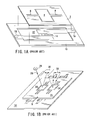
- FIGS. 1A and 1B are diagrams showing constitution examples of a conventional optical deflector
- FIGS. 3A through 3E show individual detailed constitutions of the optical deflector of FIG. 2, FIG. 3A is a top plan view, FIG. 3B is a sectional view taken along line A-A′ of FIG. 3A in a static state, FIG. 3C is a sectional view taken along line A-A′ of FIG. 3A in a driven state, FIG. 3D is a diagram showing a surface side opposite to a confronting substrate of a movable portion, and FIG. 3E is a diagram showing a mirror surface side of the movable portion;
- FIG. 4 is a top plan view showing a constitution of an optical deflector array in which optical deflectors constituted as shown in FIGS. 3A through 3E are arrayed in one row in a rock axis direction;
- FIGS. 5A through 5D show individual detailed constitutions of the optical deflector according to a second embodiment of the present invention
- FIG. 5A is a top plan view
- FIG. 5B is a sectional view in a static state
- FIG. 5C is a sectional view of a state at a driving time
- FIG. 5D is a diagram showing a mirror surface side of the movable portion
- FIGS. 6A through 6E show constitutions of the optical deflector according to a third embodiment of the present invention
- FIG. 6A is a sectional view in the static state
- FIG. 6B is a sectional view of the state at the driving time
- FIG. 6C is a top plan view
- FIG. 6D is a diagram showing the mirror surface side of the movable portion
- FIG. 6E is a diagram showing a surface side disposed opposite to the confronting substrate of the movable portion.
- FIG. 2 is a diagram showing a schematic constitution of an optical deflector array in a first embodiment of the present invention. It is to be noted that in the constitution of FIG. 2, first to third optical deflectors are shown among a plurality of optical deflectors. Moreover, only the third optical deflector is shown in a deflecting state.
- the movable plates 50 1 , 50 2 , 50 3 , elastic members 52 1 , 52 2 , 52 3 , and elastic members 54 1 , 54 2 , 54 3 are arranged to constitute first, second, and third optical deflectors 48 1 , 48 2 , 48 3 above the confronting substrate 40 . Furthermore, the movable plates 50 1 , 50 2 , 50 3 are attached between the elastic members 52 1 , 52 2 , 52 3 and elastic members 54 1 , 54 2 , 54 3 .
- the movable plates 50 1 to 50 3 are deflected by a voltage difference of voltages applied to the respective electrodes.
- the voltage difference is raised, for example, the movable plate 50 1 first contacts second convex portion 44 .
- the movable plate 50 1 in contact with an edge of the second convex portion 44 is deflected until the plate contacts the edge of the first convex portion 42 . Thereafter, even when the voltage difference is enlarged, a deflection angle does not change.
- FIGS. 3A through 3E show individual detailed constitutions of the above-described optical deflector
- FIG. 3A is a top plan view
- FIG. 3B is a sectional view taken along line A-A′ of FIG. 3A in a static state
- FIG. 3C is a sectional view taken along the line A-A′ of FIG. 3A in a driven state
- FIG. 3D is a diagram showing a surface side opposite to the confronting substrate of a movable portion
- FIG. 3E is a diagram showing a mirror surface side of the movable portion.
- the movable plate 50 , elastic members 52 , 54 , and support member 66 in FIGS. 3B, 3 C are not shown.
- the optical deflector is manufactured using the lower confronting substrate 40 , and a silicon on insulator (SOI) wafer (upper substrate) 72 .
- SOI silicon on insulator
- an insulating film (not shown) is formed on the whole surface of the confronting substrate 40 disposed opposite to the upper substrate 72 . This achieves insulation of the confronting substrate 40 from the upper substrate 72 .
- the driving electrodes 56 are disposed via the second convex portion 44 in the first convex surface 42 a , that is, an electrode substrate surface 40 b . Moreover, the edges of the second convex portion 44 are formed as a second edge 44 b.
- an upper part of the support member 66 is constituted by including the handle layer 74 .
- the movable plate 50 contacts the second edge 44 b of the second convex portion and finally contacts the first edge 42 b of the first convex portion 42 . Even when the voltage is further applied in this state, the deflection angle of the movable plate 50 does not change.
- the binary deflection angle indicates, for example, maximum deflection on one driving electrode side and maximum deflection on the other driving electrode side.
- the elastic members 52 , 54 effectively reduce the driving force of the movable plate 50 to the utmost, and selectively restrain movement in a direction other than a driving direction. This is achieved by the following function.
- the movement of the elastic members 52 , 54 depends on the movable plate 50 , and symmetric deformation occurs centering on two elastic member rock axes which support the movable plate 50 .
- the elastic members 52 , 54 are bent/deformed upwards or downwards, and further pulled in a direction (first direction) crossing at right angles to the rock axis. This is caused by the elastic members 52 , 54 which support the movable plate 50 on opposite sides, and increases the driving force necessary for the deflection angle of the movable plate 50 .
- the bent portions 82 are disposed in optimum positions in order to maintain the rigidity with respect to a rock axis direction (second direction) of the movable plate 50 .
- the connection plate 90 is disposed between the bent portions 82 and support member 66 , the rigidity with respect to a desired driving direction can be increased as compared with the rigidity with respect to the rock axis direction of the movable plate 50 . Therefore, the elastic members 52 , 54 in the present constitution can be inhibited from vibrating in the rock axis direction by an external force.
- the elastic members 52 , 54 for supporting the movable plate 50 are formed in the direction crossing at right angles to the rock axis O (first direction), and there is therefore an advantage that the opposite sides of the movable plate 50 in the rock axis direction can freely be used.
- the present constitution is used as a micro optical deflection element in a scanning type optical apparatus described in the above-described Jpn. Pat. Appln. KOKAI Publication No. 2001-116696, as shown in FIG. 4, the present optical deflectors are arrayed in one row in the rock axis direction to form the optical deflector array.
- a plurality of optical deflectors for example, five optical deflectors in this case are arranged in the direction crossing at right angles to the rock axis O.
- the metal thin films formed on the respective movable plates are electrically conducted, and can be used as a common electrode.
- a common ground can be used in a driving system using the electrostatic. attraction force.
- only by one lead-out electrode for ground formed in the terminal end of the array can be drawn out to an external ground.
- FIGS. 5A through 5D show individual detailed constitutions of the optical deflector according to the second embodiment
- FIG. 5A is a top plan view
- FIG. 5B is a sectional view in a static state
- FIG. 5C is a sectional view of a state at a driving time
- FIG. 5D is a diagram showing a mirror surface side of the movable portion. Additionally, in FIG. 5A, for ease of description, the movable plate 50 , elastic member 96 , and support member 74 in FIGS. 5B, 5 C are not shown.
- a support portion 102 is formed in an end of an confronting substrate 100 , and a first convex portion 106 is formed substantially in a middle portion. Moreover, a second concave portion 108 is formed in the vicinity of the rock axis of a movable plate 122 described later on the first convex portion 106 .
- the first convex portion 106 is formed to include an end slightly inside the end of the movable plate 122 . Furthermore, the edge of the first convex portion 106 forms an end contact portion 106 a which contacts the deflected movable plate 122 .
- the upper substrate is constituted of the movable plate 122 , and two elastic members 114 and 116 which are disposed opposite to each other via the movable plate 122 in order to support the movable plate 122 and a bond support portion 132 , respectively.
- the elastic members 114 and 116 are formed of a polyimide film 124 .
- the polyimide film 124 constitutes the elastic members 114 and 116 , and is formed while two elastic members 114 and 116 are connected to each other through the movable plate 122 .
Abstract
Description
Claims (18)
Applications Claiming Priority (2)
| Application Number | Priority Date | Filing Date | Title |
|---|---|---|---|
| JP2001390217A JP4036643B2 (en) | 2001-12-21 | 2001-12-21 | Optical deflector and optical deflector array |
| JP2001-390217 | 2001-12-21 |
Publications (2)
| Publication Number | Publication Date |
|---|---|
| US20030117687A1 US20030117687A1 (en) | 2003-06-26 |
| US6747786B2 true US6747786B2 (en) | 2004-06-08 |
Family
ID=19188350
Family Applications (1)
| Application Number | Title | Priority Date | Filing Date |
|---|---|---|---|
| US10/317,548 Expired - Lifetime US6747786B2 (en) | 2001-12-21 | 2002-12-12 | Optical deflector and optical deflector array |
Country Status (2)
| Country | Link |
|---|---|
| US (1) | US6747786B2 (en) |
| JP (1) | JP4036643B2 (en) |
Cited By (8)
| Publication number | Priority date | Publication date | Assignee | Title |
|---|---|---|---|---|
| US20040184134A1 (en) * | 2003-01-16 | 2004-09-23 | Tomohiro Makigaki | Optical modulator, display device and manufacturing method for same |
| US20040207939A1 (en) * | 2002-09-26 | 2004-10-21 | Seiko Epson Corporation | Mirror device, optical switch, electronic instrument and mirror device driving method |
| US20040212868A1 (en) * | 2003-04-22 | 2004-10-28 | Taiwan Semiconductor Manufacturing Co. | Trench-embeded mirror structure for double substrate spatial light modulator |
| US20040212907A1 (en) * | 2003-04-24 | 2004-10-28 | Mohiuddin Mala | Micro-electro-mechanical-system two dimensional mirror with articulated suspension structures for high fill factor arrays |
| US20040245889A1 (en) * | 2002-02-28 | 2004-12-09 | Pts Corporation | Systems and methods for overcoming stiction |
| US20050140834A1 (en) * | 2003-12-26 | 2005-06-30 | Fuji Photo Film Co., Ltd. | Image displaying method and device and image displaying control method and apparatus |
| US20060222312A1 (en) * | 2005-02-16 | 2006-10-05 | Mohiuddin Mala | Articulated MEMs structures |
| US20100118372A1 (en) * | 2007-04-19 | 2010-05-13 | Mitsuo Usui | Micromirror device and micromirror array |
Families Citing this family (3)
| Publication number | Priority date | Publication date | Assignee | Title |
|---|---|---|---|---|
| JP2005092174A (en) * | 2003-08-12 | 2005-04-07 | Fujitsu Ltd | Micro-oscillation element |
| JP2005345748A (en) * | 2004-06-03 | 2005-12-15 | Brother Ind Ltd | Mirror driving apparatus and retina scanning display with same |
| DE102018207783B4 (en) * | 2018-05-17 | 2022-11-10 | Fraunhofer-Gesellschaft zur Förderung der angewandten Forschung e.V. | MEMS array made of MEMS, each with a movable structural element |
Citations (10)
| Publication number | Priority date | Publication date | Assignee | Title |
|---|---|---|---|---|
| US4317611A (en) | 1980-05-19 | 1982-03-02 | International Business Machines Corporation | Optical ray deflection apparatus |
| US5554851A (en) | 1991-09-24 | 1996-09-10 | Canon Kabushiki Kaisha | Parallel plane holding mechanism and apparatus using such a mechanism |
| US6147790A (en) * | 1998-06-02 | 2000-11-14 | Texas Instruments Incorporated | Spring-ring micromechanical device |
| JP2001116696A (en) | 1999-10-21 | 2001-04-27 | Olympus Optical Co Ltd | Scanning optical device |
| US6404534B1 (en) * | 1999-10-29 | 2002-06-11 | Samsung Electronics Co., Ltd. | Micro-mirror device and driving method |
| US6438282B1 (en) * | 1998-01-20 | 2002-08-20 | Seiko Epson Corporation | Optical switching device and image display device |
| US20030123125A1 (en) * | 2000-03-20 | 2003-07-03 | Np Photonics, Inc. | Detunable Fabry-Perot interferometer and an add/drop multiplexer using the same |
| US6600591B2 (en) * | 2001-06-12 | 2003-07-29 | Network Photonics, Inc. | Micromirror array having adjustable mirror angles |
| US6603591B2 (en) * | 2001-03-29 | 2003-08-05 | Japan Aviation Electronics Industry, Ltd. | Microminiature movable device |
| US6614581B2 (en) * | 2001-07-03 | 2003-09-02 | Network Photonics, Inc. | Methods and apparatus for providing a multi-stop micromirror |
-
2001
- 2001-12-21 JP JP2001390217A patent/JP4036643B2/en not_active Expired - Fee Related
-
2002
- 2002-12-12 US US10/317,548 patent/US6747786B2/en not_active Expired - Lifetime
Patent Citations (10)
| Publication number | Priority date | Publication date | Assignee | Title |
|---|---|---|---|---|
| US4317611A (en) | 1980-05-19 | 1982-03-02 | International Business Machines Corporation | Optical ray deflection apparatus |
| US5554851A (en) | 1991-09-24 | 1996-09-10 | Canon Kabushiki Kaisha | Parallel plane holding mechanism and apparatus using such a mechanism |
| US6438282B1 (en) * | 1998-01-20 | 2002-08-20 | Seiko Epson Corporation | Optical switching device and image display device |
| US6147790A (en) * | 1998-06-02 | 2000-11-14 | Texas Instruments Incorporated | Spring-ring micromechanical device |
| JP2001116696A (en) | 1999-10-21 | 2001-04-27 | Olympus Optical Co Ltd | Scanning optical device |
| US6404534B1 (en) * | 1999-10-29 | 2002-06-11 | Samsung Electronics Co., Ltd. | Micro-mirror device and driving method |
| US20030123125A1 (en) * | 2000-03-20 | 2003-07-03 | Np Photonics, Inc. | Detunable Fabry-Perot interferometer and an add/drop multiplexer using the same |
| US6603591B2 (en) * | 2001-03-29 | 2003-08-05 | Japan Aviation Electronics Industry, Ltd. | Microminiature movable device |
| US6600591B2 (en) * | 2001-06-12 | 2003-07-29 | Network Photonics, Inc. | Micromirror array having adjustable mirror angles |
| US6614581B2 (en) * | 2001-07-03 | 2003-09-02 | Network Photonics, Inc. | Methods and apparatus for providing a multi-stop micromirror |
Cited By (20)
| Publication number | Priority date | Publication date | Assignee | Title |
|---|---|---|---|---|
| US20040245889A1 (en) * | 2002-02-28 | 2004-12-09 | Pts Corporation | Systems and methods for overcoming stiction |
| US6856069B2 (en) * | 2002-02-28 | 2005-02-15 | Pts Corporation | Systems and methods for overcoming stiction |
| US20050207042A1 (en) * | 2002-09-26 | 2005-09-22 | Seiko Epson Corporation | Mirror device, optical switch, electronic instrument and mirror device driving method |
| US6972884B2 (en) | 2002-09-26 | 2005-12-06 | Seiko Epson Corporation | Mirror device, optical switch, electronic instrument and mirror device driving method |
| US7016100B2 (en) | 2002-09-26 | 2006-03-21 | Seiko Epson Corporation | Electronic instrument having mirror device |
| US20040207939A1 (en) * | 2002-09-26 | 2004-10-21 | Seiko Epson Corporation | Mirror device, optical switch, electronic instrument and mirror device driving method |
| US20050185310A1 (en) * | 2002-09-26 | 2005-08-25 | Seiko Epson Corporation | Mirror device, optical switch, electronic instrument and mirror device driving method |
| US6914712B2 (en) * | 2002-09-26 | 2005-07-05 | Seiko Epson Corporation | Mirror device, optical switch, electronic instrument and mirror device driving method |
| US20040184134A1 (en) * | 2003-01-16 | 2004-09-23 | Tomohiro Makigaki | Optical modulator, display device and manufacturing method for same |
| US7034981B2 (en) * | 2003-01-16 | 2006-04-25 | Seiko Epson Corporation | Optical modulator, display device and manufacturing method for same |
| US6947196B2 (en) * | 2003-04-22 | 2005-09-20 | Taiwan Semiconductor Manufacturing Co., Ltd. | Trench-embedded mirror structure for double substrate spatial light modulator |
| US20040212868A1 (en) * | 2003-04-22 | 2004-10-28 | Taiwan Semiconductor Manufacturing Co. | Trench-embeded mirror structure for double substrate spatial light modulator |
| US20040212907A1 (en) * | 2003-04-24 | 2004-10-28 | Mohiuddin Mala | Micro-electro-mechanical-system two dimensional mirror with articulated suspension structures for high fill factor arrays |
| US7095546B2 (en) | 2003-04-24 | 2006-08-22 | Metconnex Canada Inc. | Micro-electro-mechanical-system two dimensional mirror with articulated suspension structures for high fill factor arrays |
| US20050140834A1 (en) * | 2003-12-26 | 2005-06-30 | Fuji Photo Film Co., Ltd. | Image displaying method and device and image displaying control method and apparatus |
| US7256551B2 (en) * | 2003-12-26 | 2007-08-14 | Fujifilm Corporation | Image displaying method and device and image displaying control method and apparatus |
| US20060222312A1 (en) * | 2005-02-16 | 2006-10-05 | Mohiuddin Mala | Articulated MEMs structures |
| US7432629B2 (en) | 2005-02-16 | 2008-10-07 | Jds Uniphase Corporation | Articulated MEMs structures |
| US20100118372A1 (en) * | 2007-04-19 | 2010-05-13 | Mitsuo Usui | Micromirror device and micromirror array |
| US8599460B2 (en) * | 2007-04-19 | 2013-12-03 | Nippon Telegraph And Telephone Corporation | Micromirror device and micromirror array |
Also Published As
| Publication number | Publication date |
|---|---|
| US20030117687A1 (en) | 2003-06-26 |
| JP2003195204A (en) | 2003-07-09 |
| JP4036643B2 (en) | 2008-01-23 |
Similar Documents
| Publication | Publication Date | Title |
|---|---|---|
| US7054048B2 (en) | Shape variable mirror | |
| US7256926B2 (en) | Optical deflector | |
| US7224507B2 (en) | Optical deflector | |
| US9632309B2 (en) | Piezoelectric and electromagnetic type two-dimensional optical deflector and its manufacturing method | |
| US7031041B2 (en) | Micro-oscillating element provided with torsion bar | |
| US5543956A (en) | Torsional vibrators and light deflectors using the torsional vibrator | |
| US7466474B2 (en) | Micromechanical device with tilted electrodes | |
| JP4541627B2 (en) | Micro mirror | |
| US6747786B2 (en) | Optical deflector and optical deflector array | |
| CN107942509B (en) | Micro mirror with distributed elastic structure | |
| US7271946B2 (en) | Micromirror and micromirror device | |
| JP3076465B2 (en) | Micro actuator and optical deflector | |
| US11675184B2 (en) | Light deflector | |
| WO2000050950A1 (en) | Planar optical scanner and its mounting structure | |
| JP2005169553A (en) | Micro-actuator | |
| KR20030067491A (en) | Resonant thermal out-of-plane buckle-beam actuator | |
| US8305671B2 (en) | Biaxial scanning mirror for image forming apparatus and method for operating the same | |
| JP2013138601A (en) | Planar type electromagnetic actuator | |
| JP2003262803A (en) | Movable structure, and deflecting mirror element, optical switch element, and shape variable mirror each using the same | |
| Mack et al. | CROSS-REFERENCE TO RELATED APPLICATIONS | |
| EP2844611B1 (en) | Mems device | |
| US6490073B2 (en) | Microactuator for optical switching and method for fabricating the same | |
| JP2013078206A (en) | Interdigital type actuator | |
| JP2009105031A (en) | Electrostatic actuator, microswitch, and electronic equipment | |
| KR20060010421A (en) | Dual comb electrode structure with spacing for increasing a driving angle of a mirco scanner and the micro scanner adopting the same |
Legal Events
| Date | Code | Title | Description |
|---|---|---|---|
| AS | Assignment |
Owner name: OLYMPUS OPTICAL CO., LTD., JAPAN Free format text: ASSIGNMENT OF ASSIGNORS INTEREST;ASSIGNORS:MURAKAMI, KENZI;MIYAJIMA, HIROSHI;REEL/FRAME:013579/0272 Effective date: 20021209 |
|
| AS | Assignment |
Owner name: OLYMPUS CORPORATION, JAPAN Free format text: CHANGE OF NAME;ASSIGNOR:OLYMPUS OPTICAL CO., LTD.;REEL/FRAME:015110/0531 Effective date: 20031001 |
|
| STCF | Information on status: patent grant |
Free format text: PATENTED CASE |
|
| FEPP | Fee payment procedure |
Free format text: PAYOR NUMBER ASSIGNED (ORIGINAL EVENT CODE: ASPN); ENTITY STATUS OF PATENT OWNER: LARGE ENTITY |
|
| FPAY | Fee payment |
Year of fee payment: 4 |
|
| FPAY | Fee payment |
Year of fee payment: 8 |
|
| FPAY | Fee payment |
Year of fee payment: 12 |
|
| AS | Assignment |
Owner name: OLYMPUS CORPORATION, JAPAN Free format text: CHANGE OF ADDRESS;ASSIGNOR:OLYMPUS CORPORATION;REEL/FRAME:039344/0502 Effective date: 20160401 |