US6754776B2 - Method and system for logical partitioning of cache memory structures in a partitoned computer system - Google Patents
Method and system for logical partitioning of cache memory structures in a partitoned computer system Download PDFInfo
- Publication number
- US6754776B2 US6754776B2 US09/861,258 US86125801A US6754776B2 US 6754776 B2 US6754776 B2 US 6754776B2 US 86125801 A US86125801 A US 86125801A US 6754776 B2 US6754776 B2 US 6754776B2
- Authority
- US
- United States
- Prior art keywords
- bits
- tag
- index
- address
- memory
- Prior art date
- Legal status (The legal status is an assumption and is not a legal conclusion. Google has not performed a legal analysis and makes no representation as to the accuracy of the status listed.)
- Expired - Fee Related, expires
Links
Images


Classifications
-
- G—PHYSICS
- G06—COMPUTING; CALCULATING OR COUNTING
- G06F—ELECTRIC DIGITAL DATA PROCESSING
- G06F12/00—Accessing, addressing or allocating within memory systems or architectures
- G06F12/02—Addressing or allocation; Relocation
- G06F12/08—Addressing or allocation; Relocation in hierarchically structured memory systems, e.g. virtual memory systems
- G06F12/0802—Addressing of a memory level in which the access to the desired data or data block requires associative addressing means, e.g. caches
- G06F12/0806—Multiuser, multiprocessor or multiprocessing cache systems
- G06F12/084—Multiuser, multiprocessor or multiprocessing cache systems with a shared cache
-
- G—PHYSICS
- G06—COMPUTING; CALCULATING OR COUNTING
- G06F—ELECTRIC DIGITAL DATA PROCESSING
- G06F12/00—Accessing, addressing or allocating within memory systems or architectures
- G06F12/02—Addressing or allocation; Relocation
- G06F12/08—Addressing or allocation; Relocation in hierarchically structured memory systems, e.g. virtual memory systems
- G06F12/0802—Addressing of a memory level in which the access to the desired data or data block requires associative addressing means, e.g. caches
- G06F12/0806—Multiuser, multiprocessor or multiprocessing cache systems
- G06F12/0813—Multiuser, multiprocessor or multiprocessing cache systems with a network or matrix configuration
Definitions
- the present invention relates generally to the logical partitioning of a shared memory structure of a computer system. More particularly, the present invention is directed towards logical partitioning a cache memory between computer domains.
- Multinode computer networks are often partitioned into domains, with each domain functioning as an independent machine with its own address space. An operating system runs separately on each domain. Partitioning permits the resources of a computer network to be efficiently allocated to different tasks, to provide flexibility in the use of a computer system, and to provide isolation between computer resources to limit the effects of hardware or software faults in one part of the network from interfering with the operation of the entire system.
- FIG. 1 shows an illustration of a multimode computer system including central processing unit (CPU) nodes 105 , memory nodes 110 , and input/output (I/O) nodes 115 coupled to a system interconnect 120 .
- Partition definition registers may be used to partition the multimode system into domains 130 , 135 , 140 .
- each domain has its own memory structures. This can be implemented as one or more local cache memories 145 which are kept coherent via a sparse directory 147 for each domain.
- FIG. 2A illustrates a conventional addressing technique for addressing a memory structure within a domain.
- a cache memory 200 is a data array for storing sets 205 of data. Each set 205 is also sometimes described in the art as a data line.
- each cache line entry 202 stored in the cache typically has an associated tag field 206 . The value of the index 207 of the address indicates to which set 205 of the cache the address maps to.
- each set (cache address) consists of a set of K-lines of data entries, with each data entry in the set having its own tag field 206 .
- the tag bits are stored along with the data bits.
- the index 207 of the memory address is used to select a set 205 in the cache, i.e., a set 205 in the cache is indexed by the portion of the memory address called the index 207 .
- the tag 210 of the CPU memory address is compared with the tag 206 of an entry 202 from the cache. If the tags 206 and 210 match there is a hit and the desired word entry is in the cache.
- each of the K-lines in a set has its own tag and the tags for each entry are compared in parallel with the incoming address with a hit occurring if one of the tags match. Interleaving may be included so that multiple independent requests may be processed. Consequently, an interleave field 215 identifies which leaf to use. An offset field 220 identifies which data structure with the cache line is being accessed.
- FIG. 2B illustrates a conventional hardware system having comparators and multiplexors to output a signal indicative of a hit if the tag portion of the address matches the tag of an entry that is being addressed.
- FIG. 2A represents a generalized addressing system that includes a variety of special memory structures.
- a drawback of computer system 100 is that changes in domain partitioning and usage patterns may result in inefficient use of the memory hardware.
- the domain partitioning of the system may change over time to meet new needs, i.e., the computer system may be configured to change the number of domains to meet new needs.
- the total number of cache memories must be selected to be at least equal to a maximum number of domains for which computer system 100 is designed to support. If the number of domains is less than the maximum value there will be one or more idle memories. This is inefficient in regards to the use of cache memory hardware.
- the extended memory address includes an address space identifier for extending a conventional memory address with at least one bit uniquely identifying the address space of a domain from which a data request is made to the cache memory.
- the address space identifier has tag extension bits and index extension bits that are used to extend the tag bits and index bits of a conventional memory address.
- a data set in the cache memory is accessed by an index value that includes the index bits and the index extension bits and a hit is determined from a tag value that includes the tag bits and the tag extension bits.
- FIG. (“FIG.”) 1 is a block diagram of one embodiment of an overall architecture of a prior art multi-node network computer system.
- FIG. 2B illustrates a conventional K-way set associative cache memory.
- FIG. 3 is multimode computer system in accordance with the present invention in which memory structures are logically partitioned.
- FIG. 4 illustrates a memory array and address format in accordance with the present invention.
- FIG. 5 illustrates an embodiment of the memory array and address format with programmable partitioning.
- FIG. 6 illustrates a block diagram of a circuit for generating index bits for the programmable partitioning embodiment of FIG. 5 .
- the present invention includes a system and a method for a logical partition of a memory structure between computer domains.
- a multi-node network system that includes a plurality of central processing unit (CPU) nodes 105 , memory nodes 110 , and input/output (I/O) nodes 115 coupled to a system interconnect 120 .
- the system interconnect 120 may be, for example, a mesh, ring or hypercube implemented using routers or switches.
- Partition definition registers (not shown in FIG. 3 ), may be used to partition the multimode system into domains 130 , 135 , 140 .
- One aspect of the present invention is that logical partitioning of shared memory structures, such as cache memory 305 and sparse directory tables 310 , between domains is supported. This is illustrated graphically by the boundary between domains passing through a memory structure.
- the logical partitioning permits the physical memory to be shared while maintaining domain isolation. Moreover, the logical partitioning permits flexible control over how a particular memory structure is partitioned.
- Each domain of computer system 300 functions as an independent machine and consequently each machine has its own address space.
- Each domain has its own address space.
- Each address space has a set of memory addresses for accessing memory structures within the domain, such as a cache memory.
- domain 130 has an associated address space
- domain 135 has an associated address space
- domain 140 has an associated address space. The same memory address in different domains is not physically equivalent because the request originates from a different address space.
- One aspect of the present invention is a method to extend a conventional memory address of a data request originating from a domain to include an additional bit field that references the address space from which the request originates.
- each domain 135 , 135 , and 140 is assigned a unique address space identifier.
- the unique address space identifier can be any numeric value that is uniquely associated with the address space from which the request originated.
- the unique address space identifier can be a unique numeric label assigned to each domain.
- each node could be assigned a unique global identifier in the system that is used as the address space identifier. Since a domain encompasses a selected subset of the nodes, the unique global identifier of a node would identify the target address space of the request.
- the memory address has the bit field of the unique address space identifier attached as an additional bit field, such as a bit field attached as prefix bits.
- the unique address space identifier of the extended address includes additional information which permits the data entries of the shared memory structure to be allocated in a variety of different ways between shared domains, as described below in more detail.
- bits from the unique address space identifier may be combined with the index bits of the memory address to form an index value for accessing a set in the shared memory structure while bits from the unique address space identifier may be combined with the tag bits to form a tag value for determining a hit.
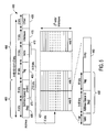
- FIG. 4 shows one embodiment of an address format 400 in accord with the present invention for accessing a memory structure 418 having a plurality of data sets 401 .
- Memory structure 418 may be a cache or other memory structures in which data sets 401 are accessible by an index value.
- the memory structure is a K-way set associative data cache where each set 401 is a set of data entries 480 having K-lines.
- Address format 400 preferably includes the bits of a conventional domain memory address 450 , such as a domain memory address having a tag field 405 for tag bits, an index field 410 for index bits, an interleave field 415 for interleave bits, and an offset field 420 for offset bits.
- the conventional domain memory address 450 is extended by the bits of a unique address space identifier field 460 .
- the unique address space identifier 460 field comprises a tag extension field 465 , such as a tag extension field with an integer number “A” of bits uses as a tag extension and an index extension field 470 having an integer number “B” of bits used as an index extension.
- FIG. 4 illustrates one embodiment in which the bit value of the index used to select a data line in a cache is a combination of the conventional index bits and the index extension bits.
- the index value used to select a data set can have a width of B+X bits wide.
- the index extension 460 is three bits wide (i.e., one unique value for each potential domain) in the system.
- Each data entry 480 in a set 401 of the cache is stored with a tag value 485 that preferably includes the bits of tag field bits 405 and the bits of tag extension field 465 .
- the present invention permits a memory structure to be used in a variety of different ways. If the index extension is non-zero, the data set entries are divided up by 2 B , where B is the number of bits of the index extension 470 . As shown in FIG. 4, there can thus be 2 x+B sets of entries in a K-way associative memory. All domains for which the address space ID has the same index extension value share the same subset of entries. If desired, however, each domain may be assigned a unique index extension value so that no domain shares a subset of entries by setting A to zero.
- the index extension field 470 is set to the same value for all domains sharing the memory structure (e.g., the B bits are set to zero). If the B bits are the same (e.g., zero) for all unique domain space identifiers, then the bit value of index field 410 is used to access a data set 401 but the tag value 485 used for a match is the value of tag field 405 plus the value of tag extension field 465 (i.e., A+W bits).
- bit value of the tag extension extension field 465 e.g., the the A bits
- the bit value of the domain tag field 405 the W bits
- the bit value of the index extension field 470 of two domains are the same, the two domains can access the same data set in the cache.
- the A bits are zero, then two domains may also have the same tag value 485 .
- This permits static allocation of entries across domains without imposing a static partition of interface bandwidth to the shared memory structure. This has the benefit of reducing the performance interaction between domains such as requests from one domain causing eviction of an entry allocated to another domain. This also has the benefit of improving fault isolation and containment such that an error in one domain does not affect another domain.
- the index extension field 470 need only be two bits long to provide four different values of the index extension.
- Each domain in such a system could be assigned different index extension encoding. This would result in each domain indexing different sets of the memory structure.
- Another benefit of the present invention is in regards to a computer system 300 having large capacity cache memory structures.
- a small number of large capacity cache memory structures may be logically partitioned to allocated cache memory for two or more domains, as described above.
- the unique address space identifier of each domain is preferably selectable by a control interface.
- the manner in which data is allocated between domains in a shared cache may also be varied by changing the bits of the unique address space identifiers.
- One embodiment of the present invention is as a single hardware implementation whose configuration is programmable, which supports flexible dynamic partitioning of the server into domains.
- the full address space identifier 460 i.e., the A and B bits
- the partitioning of the cache memory structure then becomes a function of the width of the index extension field 470 (e.g., the “B” bits) of address space identifier 460 .
- a data set 401 is indexed by the concatenation of the bits (B) of the index extension field 470 and the low (X ⁇ B) bits of the index field 410 .
- the choice of configuration is selected by setting the value of the index extension field 470 in a configuration register.
- FIG. 5 illustrates this embodiment.
- An individual data set is indexed by the concatenation of the B bits and the X ⁇ B bits of the index field 410 .
- FIG. 6 shows a hardware mechanism for generating the index field. The choice of configuration is selected by setting the value of the B bits in a configuration register.
Abstract
Description
Claims (27)
Priority Applications (2)
| Application Number | Priority Date | Filing Date | Title |
|---|---|---|---|
| US09/861,258 US6754776B2 (en) | 2001-05-17 | 2001-05-17 | Method and system for logical partitioning of cache memory structures in a partitoned computer system |
| JP2002143188A JP2003006045A (en) | 2001-05-17 | 2002-05-17 | Computer system |
Applications Claiming Priority (1)
| Application Number | Priority Date | Filing Date | Title |
|---|---|---|---|
| US09/861,258 US6754776B2 (en) | 2001-05-17 | 2001-05-17 | Method and system for logical partitioning of cache memory structures in a partitoned computer system |
Publications (2)
| Publication Number | Publication Date |
|---|---|
| US20020174301A1 US20020174301A1 (en) | 2002-11-21 |
| US6754776B2 true US6754776B2 (en) | 2004-06-22 |
Family
ID=25335299
Family Applications (1)
| Application Number | Title | Priority Date | Filing Date |
|---|---|---|---|
| US09/861,258 Expired - Fee Related US6754776B2 (en) | 2001-05-17 | 2001-05-17 | Method and system for logical partitioning of cache memory structures in a partitoned computer system |
Country Status (2)
| Country | Link |
|---|---|
| US (1) | US6754776B2 (en) |
| JP (1) | JP2003006045A (en) |
Cited By (15)
| Publication number | Priority date | Publication date | Assignee | Title |
|---|---|---|---|---|
| US20050091454A1 (en) * | 2003-10-23 | 2005-04-28 | Hitachi, Ltd. | Storage having logical partitioning capability and systems which include the storage |
| US20050129524A1 (en) * | 2001-05-18 | 2005-06-16 | Hitachi, Ltd. | Turbine blade and turbine |
| US20050172040A1 (en) * | 2004-02-03 | 2005-08-04 | Akiyoshi Hashimoto | Computer system, control apparatus, storage system and computer device |
| WO2006000138A1 (en) * | 2004-06-29 | 2006-01-05 | Deyuan Wang | A buffer apparatus and method |
| US20060294313A1 (en) * | 2005-06-23 | 2006-12-28 | International Business Machines Corporation | System and method of remote media cache optimization for use with multiple processing units |
| US7185142B2 (en) | 2004-03-17 | 2007-02-27 | Hitachi, Ltd. | Storage management method and storage management system |
| US20100217949A1 (en) * | 2009-02-24 | 2010-08-26 | International Business Machines Corporation | Dynamic Logical Partition Management For NUMA Machines And Clusters |
| US20100318975A1 (en) * | 2009-06-10 | 2010-12-16 | Microsoft Corporation | Language-based model for isolating shared state |
| WO2013142327A1 (en) * | 2012-03-23 | 2013-09-26 | Hicamp Systems, Inc. | Special memory access path with segment-offset addressing |
| US9223710B2 (en) | 2013-03-16 | 2015-12-29 | Intel Corporation | Read-write partitioning of cache memory |
| US9520193B2 (en) | 2007-01-26 | 2016-12-13 | Intel Corporation | Hierarchical immutable content-addressable memory processor |
| US9601199B2 (en) | 2007-01-26 | 2017-03-21 | Intel Corporation | Iterator register for structured memory |
| US9684602B2 (en) | 2015-03-11 | 2017-06-20 | Kabushiki Kaisha Toshiba | Memory access control device, cache memory and semiconductor device |
| US9792214B2 (en) | 2014-09-08 | 2017-10-17 | Toshiba Memory Corporation | Cache memory for particular data |
| US9990288B2 (en) | 2014-03-13 | 2018-06-05 | Kabushiki Kaisha Toshiba | Information processing device and data structure |
Families Citing this family (20)
| Publication number | Priority date | Publication date | Assignee | Title |
|---|---|---|---|---|
| US7054867B2 (en) * | 2001-09-18 | 2006-05-30 | Skyris Networks, Inc. | Systems, methods and programming for routing and indexing globally addressable objects and associated business models |
| WO2003048955A1 (en) * | 2001-12-03 | 2003-06-12 | Hitachi, Ltd. | Multi-processor system |
| DE602004029870D1 (en) * | 2003-03-06 | 2010-12-16 | Nxp Bv | DATA PROCESSING SYSTEM WITH A CACHE OPTIMIZED FOR PROCESSING DATA FLOW APPLICATIONS |
| WO2006082554A2 (en) * | 2005-02-02 | 2006-08-10 | Koninklijke Philips Electronics N.V. | Data processing system comprising a cache unit |
| US20090019306A1 (en) * | 2007-07-11 | 2009-01-15 | Herbert Hum | Protecting tag information in a multi-level cache hierarchy |
| US8095736B2 (en) * | 2008-02-25 | 2012-01-10 | Telefonaktiebolaget Lm Ericsson (Publ) | Methods and systems for dynamic cache partitioning for distributed applications operating on multiprocessor architectures |
| JP5275673B2 (en) * | 2008-04-23 | 2013-08-28 | トヨタ自動車株式会社 | Multi-core system, vehicle gateway device |
| US20090300293A1 (en) * | 2008-05-30 | 2009-12-03 | Advanced Micro Devices, Inc. | Dynamically Partitionable Cache |
| US8244982B2 (en) * | 2009-08-21 | 2012-08-14 | Empire Technology Development Llc | Allocating processor cores with cache memory associativity |
| US8364922B2 (en) | 2009-12-21 | 2013-01-29 | International Business Machines Corporation | Aggregate symmetric multiprocessor system |
| WO2011076599A1 (en) * | 2009-12-21 | 2011-06-30 | International Business Machines Corporation | Aggregate symmetric multiprocessor system |
| US9836400B2 (en) * | 2013-10-31 | 2017-12-05 | Intel Corporation | Method, apparatus and system for dynamically controlling an addressing mode for a cache memory |
| US9436619B2 (en) * | 2014-09-08 | 2016-09-06 | Raytheon Company | Multi-level, hardware-enforced domain separation using a separation kernel on a multicore processor with a shared cache |
| US20170344297A1 (en) * | 2016-05-26 | 2017-11-30 | Microsoft Technology Licensing, Llc | Memory attribution and control |
| US10908915B1 (en) * | 2019-07-31 | 2021-02-02 | Micron Technology, Inc. | Extended tags for speculative and normal executions |
| US11200166B2 (en) | 2019-07-31 | 2021-12-14 | Micron Technology, Inc. | Data defined caches for speculative and normal executions |
| US11048636B2 (en) | 2019-07-31 | 2021-06-29 | Micron Technology, Inc. | Cache with set associativity having data defined cache sets |
| US11194582B2 (en) | 2019-07-31 | 2021-12-07 | Micron Technology, Inc. | Cache systems for main and speculative threads of processors |
| US10915326B1 (en) | 2019-07-31 | 2021-02-09 | Micron Technology, Inc. | Cache systems and circuits for syncing caches or cache sets |
| US11010288B2 (en) | 2019-07-31 | 2021-05-18 | Micron Technology, Inc. | Spare cache set to accelerate speculative execution, wherein the spare cache set, allocated when transitioning from non-speculative execution to speculative execution, is reserved during previous transitioning from the non-speculative execution to the speculative execution |
Citations (23)
| Publication number | Priority date | Publication date | Assignee | Title |
|---|---|---|---|---|
| US5175839A (en) | 1987-12-24 | 1992-12-29 | Fujitsu Limited | Storage control system in a computer system for double-writing |
| US5465338A (en) | 1993-08-24 | 1995-11-07 | Conner Peripherals, Inc. | Disk drive system interface architecture employing state machines |
| US5561780A (en) | 1993-12-30 | 1996-10-01 | Intel Corporation | Method and apparatus for combining uncacheable write data into cache-line-sized write buffers |
| US5592671A (en) | 1993-03-02 | 1997-01-07 | Kabushiki Kaisha Toshiba | Resource management system and method |
| US5727150A (en) | 1995-05-05 | 1998-03-10 | Silicon Graphics, Inc. | Apparatus and method for page migration in a non-uniform memory access (NUMA) system |
| US5761460A (en) | 1996-07-19 | 1998-06-02 | Compaq Computer Corporation | Reconfigurable dual master IDE interface |
| US5809535A (en) * | 1995-04-14 | 1998-09-15 | Nec Corporation | Cache memory control apparatus utilizing a bit as a second valid bit in a tag in a first mode and as an additional address bit in a second mode |
| US5829032A (en) | 1994-10-31 | 1998-10-27 | Kabushiki Kaisha Toshiba | Multiprocessor system |
| US5859985A (en) | 1996-01-14 | 1999-01-12 | At&T Wireless Services, Inc. | Arbitration controller for providing arbitration on a multipoint high speed serial bus using drivers having output enable pins |
| US5887134A (en) | 1997-06-30 | 1999-03-23 | Sun Microsystems | System and method for preserving message order while employing both programmed I/O and DMA operations |
| US6006255A (en) | 1996-04-05 | 1999-12-21 | International Business Machines Corporation | Networked computer system and method of communicating using multiple request packet classes to prevent deadlock |
| US6014690A (en) | 1997-10-24 | 2000-01-11 | Digital Equipment Corporation | Employing multiple channels for deadlock avoidance in a cache coherency protocol |
| US6026472A (en) | 1997-06-24 | 2000-02-15 | Intel Corporation | Method and apparatus for determining memory page access information in a non-uniform memory access computer system |
| US6192458B1 (en) * | 1998-03-23 | 2001-02-20 | International Business Machines Corporation | High performance cache directory addressing scheme for variable cache sizes utilizing associativity |
| US20020184345A1 (en) | 2001-05-17 | 2002-12-05 | Kazunori Masuyama | System and Method for partitioning a computer system into domains |
| US6493812B1 (en) * | 1999-12-17 | 2002-12-10 | Hewlett-Packard Company | Apparatus and method for virtual address aliasing and multiple page size support in a computer system having a prevalidated cache |
| US6493800B1 (en) * | 1999-03-31 | 2002-12-10 | International Business Machines Corporation | Method and system for dynamically partitioning a shared cache |
| US20020186711A1 (en) | 2001-05-17 | 2002-12-12 | Kazunori Masuyama | Fault containment and error handling in a partitioned system with shared resources |
| US20030005070A1 (en) | 2001-06-29 | 2003-01-02 | Narasimhamurthy Prabhunandan B. | Dynamic determination of memory mapped input output range granularity for multi-node computer system |
| US20030005156A1 (en) | 2001-06-29 | 2003-01-02 | Sudheer Miryala | Scalable and flexible method for address space decoding in a multiple node computer system |
| US20030007457A1 (en) | 2001-06-29 | 2003-01-09 | Farrell Jeremy J. | Hardware mechanism to improve performance in a multi-node computer system |
| US20030007493A1 (en) | 2001-06-28 | 2003-01-09 | Hitoshi Oi | Routing mechanism for static load balancing in a partitioned computer system with a fully connected network |
| US20030023666A1 (en) | 2001-06-28 | 2003-01-30 | Conway Patrick N. | System and method for low overhead message passing between domains in a partitioned server |
-
2001
- 2001-05-17 US US09/861,258 patent/US6754776B2/en not_active Expired - Fee Related
-
2002
- 2002-05-17 JP JP2002143188A patent/JP2003006045A/en active Pending
Patent Citations (23)
| Publication number | Priority date | Publication date | Assignee | Title |
|---|---|---|---|---|
| US5175839A (en) | 1987-12-24 | 1992-12-29 | Fujitsu Limited | Storage control system in a computer system for double-writing |
| US5592671A (en) | 1993-03-02 | 1997-01-07 | Kabushiki Kaisha Toshiba | Resource management system and method |
| US5465338A (en) | 1993-08-24 | 1995-11-07 | Conner Peripherals, Inc. | Disk drive system interface architecture employing state machines |
| US5561780A (en) | 1993-12-30 | 1996-10-01 | Intel Corporation | Method and apparatus for combining uncacheable write data into cache-line-sized write buffers |
| US5829032A (en) | 1994-10-31 | 1998-10-27 | Kabushiki Kaisha Toshiba | Multiprocessor system |
| US5809535A (en) * | 1995-04-14 | 1998-09-15 | Nec Corporation | Cache memory control apparatus utilizing a bit as a second valid bit in a tag in a first mode and as an additional address bit in a second mode |
| US5727150A (en) | 1995-05-05 | 1998-03-10 | Silicon Graphics, Inc. | Apparatus and method for page migration in a non-uniform memory access (NUMA) system |
| US5859985A (en) | 1996-01-14 | 1999-01-12 | At&T Wireless Services, Inc. | Arbitration controller for providing arbitration on a multipoint high speed serial bus using drivers having output enable pins |
| US6006255A (en) | 1996-04-05 | 1999-12-21 | International Business Machines Corporation | Networked computer system and method of communicating using multiple request packet classes to prevent deadlock |
| US5761460A (en) | 1996-07-19 | 1998-06-02 | Compaq Computer Corporation | Reconfigurable dual master IDE interface |
| US6026472A (en) | 1997-06-24 | 2000-02-15 | Intel Corporation | Method and apparatus for determining memory page access information in a non-uniform memory access computer system |
| US5887134A (en) | 1997-06-30 | 1999-03-23 | Sun Microsystems | System and method for preserving message order while employing both programmed I/O and DMA operations |
| US6014690A (en) | 1997-10-24 | 2000-01-11 | Digital Equipment Corporation | Employing multiple channels for deadlock avoidance in a cache coherency protocol |
| US6192458B1 (en) * | 1998-03-23 | 2001-02-20 | International Business Machines Corporation | High performance cache directory addressing scheme for variable cache sizes utilizing associativity |
| US6493800B1 (en) * | 1999-03-31 | 2002-12-10 | International Business Machines Corporation | Method and system for dynamically partitioning a shared cache |
| US6493812B1 (en) * | 1999-12-17 | 2002-12-10 | Hewlett-Packard Company | Apparatus and method for virtual address aliasing and multiple page size support in a computer system having a prevalidated cache |
| US20020184345A1 (en) | 2001-05-17 | 2002-12-05 | Kazunori Masuyama | System and Method for partitioning a computer system into domains |
| US20020186711A1 (en) | 2001-05-17 | 2002-12-12 | Kazunori Masuyama | Fault containment and error handling in a partitioned system with shared resources |
| US20030007493A1 (en) | 2001-06-28 | 2003-01-09 | Hitoshi Oi | Routing mechanism for static load balancing in a partitioned computer system with a fully connected network |
| US20030023666A1 (en) | 2001-06-28 | 2003-01-30 | Conway Patrick N. | System and method for low overhead message passing between domains in a partitioned server |
| US20030005070A1 (en) | 2001-06-29 | 2003-01-02 | Narasimhamurthy Prabhunandan B. | Dynamic determination of memory mapped input output range granularity for multi-node computer system |
| US20030005156A1 (en) | 2001-06-29 | 2003-01-02 | Sudheer Miryala | Scalable and flexible method for address space decoding in a multiple node computer system |
| US20030007457A1 (en) | 2001-06-29 | 2003-01-09 | Farrell Jeremy J. | Hardware mechanism to improve performance in a multi-node computer system |
Non-Patent Citations (13)
| Title |
|---|
| Abandah, Gheith A., et al. Effects of Architectural and Technological Advances on the HP/Convex Exemplar's Memory and Communication Performance, 1998 25<th >International Symposium on Computer Architecture, pp. 318-329;. |
| Abandah, Gheith A., et al. Effects of Architectural and Technological Advances on the HP/Convex Exemplar's Memory and Communication Performance, 1998 25th International Symposium on Computer Architecture, pp. 318-329;. |
| Falsafi, Babak et al., Reaactive NUMA: A design for Unifying S-COMA and CC-NUMA , 1997 24<th >International Symposium on Computer Architecture, pp. 229-240. |
| Falsafi, Babak et al., Reaactive NUMA: A design for Unifying S-COMA and CC-NUMA , 1997 24th International Symposium on Computer Architecture, pp. 229-240. |
| Geralds, John in Silcon Valley. Sun enhances partitoning in Starfire Unix server. Dec. 08, 1999. VNU Business Publishing Limited [retrieved on 2001-04-11]. Retrieved from the internet: URL:http//www.vnunet.com/print/104311. |
| IBM. The IBM NUMA-Q enterprise server architecture. Solving issues of latency and scalability in multiprocessor sytems. Jan. 19, 2000, 10 pages. |
| Lovett, Tom et al., StinNG: A CC-NUMA Computer System for the Commercial Marketplace, 1996 23<23>International Symposium on Computer Architecture, pp. 308-317. |
| Lovett, Tom et al., StinNG: A CC-NUMA Computer System for the Commercial Marketplace, 1996 2323International Symposium on Computer Architecture, pp. 308-317. |
| Servers White Paper. Sun Enterprise (TM)1000 Server: Dynamic System Domains . Sun Microsystems, Inc., Palo Alto, CA, USA. 2001. [retrieved on 2001-04-11]. Retrieved from the internet: URL:http://www.sun.com./servers/white-papers/domains.html?pagestyle=print. |
| Servers White Paper. Sun Enterprise ™1000 Server: Dynamic System Domains . Sun Microsystems, Inc., Palo Alto, CA, USA. 2001. [retrieved on 2001-04-11]. Retrieved from the internet: URL:http://www.sun.com./servers/white-papers/domains.html?pagestyle=print. |
| Unisys White Paper. Cellular Multiprocessing Shared Memory: Shared Memory and Windows, Sep. 2000, pp. 1-16. |
| Willard, Christopher,an IDC White Paper. Superdome -Hewelett-Packard Extends Its High-End Computing Capabilities, (2000), pp. 1-20. |
| Willard, Christopher,an IDC White Paper. Superdome —Hewelett-Packard Extends Its High-End Computing Capabilities, (2000), pp. 1-20. |
Cited By (41)
| Publication number | Priority date | Publication date | Assignee | Title |
|---|---|---|---|---|
| US20050129524A1 (en) * | 2001-05-18 | 2005-06-16 | Hitachi, Ltd. | Turbine blade and turbine |
| US8386721B2 (en) | 2003-10-23 | 2013-02-26 | Hitachi, Ltd. | Storage having logical partitioning capability and systems which include the storage |
| US20050091453A1 (en) * | 2003-10-23 | 2005-04-28 | Kentaro Shimada | Storage having logical partitioning capability and systems which include the storage |
| US7546426B2 (en) | 2003-10-23 | 2009-06-09 | Hitachi, Ltd. | Storage having a logical partitioning capability and systems which include the storage |
| US20050091454A1 (en) * | 2003-10-23 | 2005-04-28 | Hitachi, Ltd. | Storage having logical partitioning capability and systems which include the storage |
| US20070106872A1 (en) * | 2003-10-23 | 2007-05-10 | Kentaro Shimada | Storage having a logical partitioning capability and systems which include the storage |
| US7181577B2 (en) | 2003-10-23 | 2007-02-20 | Hitachi, Ltd. | Storage having logical partitioning capability and systems which include the storage |
| US7127585B2 (en) | 2003-10-23 | 2006-10-24 | Hitachi, Ltd. | Storage having logical partitioning capability and systems which include the storage |
| US20050172040A1 (en) * | 2004-02-03 | 2005-08-04 | Akiyoshi Hashimoto | Computer system, control apparatus, storage system and computer device |
| US7093035B2 (en) | 2004-02-03 | 2006-08-15 | Hitachi, Ltd. | Computer system, control apparatus, storage system and computer device |
| US8176211B2 (en) | 2004-02-03 | 2012-05-08 | Hitachi, Ltd. | Computer system, control apparatus, storage system and computer device |
| US8495254B2 (en) | 2004-02-03 | 2013-07-23 | Hitachi, Ltd. | Computer system having virtual storage apparatuses accessible by virtual machines |
| US20050240800A1 (en) * | 2004-02-03 | 2005-10-27 | Hitachi, Ltd. | Computer system, control apparatus, storage system and computer device |
| US20090157926A1 (en) * | 2004-02-03 | 2009-06-18 | Akiyoshi Hashimoto | Computer system, control apparatus, storage system and computer device |
| US7519745B2 (en) | 2004-02-03 | 2009-04-14 | Hitachi, Ltd. | Computer system, control apparatus, storage system and computer device |
| US7415578B2 (en) | 2004-03-17 | 2008-08-19 | Hitachi, Ltd. | Storage management method and storage management system |
| US7185142B2 (en) | 2004-03-17 | 2007-02-27 | Hitachi, Ltd. | Storage management method and storage management system |
| US8209495B2 (en) | 2004-03-17 | 2012-06-26 | Hitachi, Ltd. | Storage management method and storage management system |
| US7287129B2 (en) | 2004-03-17 | 2007-10-23 | Hitachi, Ltd. | Storage management method and storage management system |
| US20080282043A1 (en) * | 2004-03-17 | 2008-11-13 | Shuichi Yagi | Storage management method and storage management system |
| US20110173390A1 (en) * | 2004-03-17 | 2011-07-14 | Shuichi Yagi | Storage management method and storage management system |
| US7917704B2 (en) | 2004-03-17 | 2011-03-29 | Hitachi, Ltd. | Storage management method and storage management system |
| US20070233958A1 (en) * | 2004-06-29 | 2007-10-04 | Deyuan Wang | Cashe Device and Method for the Same |
| US7627719B2 (en) | 2004-06-29 | 2009-12-01 | Deyuan Wang | Cache device and method for determining LRU identifier by pointer values |
| WO2006000138A1 (en) * | 2004-06-29 | 2006-01-05 | Deyuan Wang | A buffer apparatus and method |
| US20060294313A1 (en) * | 2005-06-23 | 2006-12-28 | International Business Machines Corporation | System and method of remote media cache optimization for use with multiple processing units |
| US10282122B2 (en) | 2007-01-26 | 2019-05-07 | Intel Corporation | Methods and systems of a memory controller for hierarchical immutable content-addressable memory processor |
| US9952972B2 (en) | 2007-01-26 | 2018-04-24 | Intel Corporation | Iterator register for structured memory |
| US9520193B2 (en) | 2007-01-26 | 2016-12-13 | Intel Corporation | Hierarchical immutable content-addressable memory processor |
| US9870824B2 (en) | 2007-01-26 | 2018-01-16 | Intel Corporation | Iterator register for structured memory |
| US9601199B2 (en) | 2007-01-26 | 2017-03-21 | Intel Corporation | Iterator register for structured memory |
| US20100217949A1 (en) * | 2009-02-24 | 2010-08-26 | International Business Machines Corporation | Dynamic Logical Partition Management For NUMA Machines And Clusters |
| US8140817B2 (en) * | 2009-02-24 | 2012-03-20 | International Business Machines Corporation | Dynamic logical partition management for NUMA machines and clusters |
| US9753698B2 (en) * | 2009-06-10 | 2017-09-05 | Microsoft Technology Licensing, Llc | Language-based model for isolating shared state |
| US20100318975A1 (en) * | 2009-06-10 | 2010-12-16 | Microsoft Corporation | Language-based model for isolating shared state |
| WO2013142327A1 (en) * | 2012-03-23 | 2013-09-26 | Hicamp Systems, Inc. | Special memory access path with segment-offset addressing |
| US9223710B2 (en) | 2013-03-16 | 2015-12-29 | Intel Corporation | Read-write partitioning of cache memory |
| US9990288B2 (en) | 2014-03-13 | 2018-06-05 | Kabushiki Kaisha Toshiba | Information processing device and data structure |
| US9792214B2 (en) | 2014-09-08 | 2017-10-17 | Toshiba Memory Corporation | Cache memory for particular data |
| US10191846B2 (en) | 2014-09-08 | 2019-01-29 | Toshiba Memory Corporation | Cache memory for particular data |
| US9684602B2 (en) | 2015-03-11 | 2017-06-20 | Kabushiki Kaisha Toshiba | Memory access control device, cache memory and semiconductor device |
Also Published As
| Publication number | Publication date |
|---|---|
| JP2003006045A (en) | 2003-01-10 |
| US20020174301A1 (en) | 2002-11-21 |
Similar Documents
| Publication | Publication Date | Title |
|---|---|---|
| US6754776B2 (en) | Method and system for logical partitioning of cache memory structures in a partitoned computer system | |
| US4980822A (en) | Multiprocessing system having nodes containing a processor and an associated memory module with dynamically allocated local/global storage in the memory modules | |
| US9032143B2 (en) | Enhanced memory savings in routing memory structures of serial attached SCSI expanders | |
| US9264357B2 (en) | Apparatus and method for table search with centralized memory pool in a network switch | |
| US7373514B2 (en) | High-performance hashing system | |
| US7058642B2 (en) | Method and data structure for a low memory overhead database | |
| US7606236B2 (en) | Forwarding information base lookup method | |
| US6434144B1 (en) | Multi-level table lookup | |
| US6922766B2 (en) | Remote translation mechanism for a multi-node system | |
| US6725216B2 (en) | Partitioning search key thereby distributing table across multiple non-contiguous memory segments, memory banks or memory modules | |
| US5813001A (en) | Method for performing optimized intelligent searches of knowledge bases using submaps associated with search objects | |
| WO2001005116A2 (en) | Routing method and apparatus | |
| JP4348093B2 (en) | Accessing memory in an interleaved manner using a map table | |
| US6351798B1 (en) | Address resolution unit and address resolution method for a multiprocessor system | |
| US6279097B1 (en) | Method and apparatus for adaptive address lookup table generator for networking application | |
| US6094710A (en) | Method and system for increasing system memory bandwidth within a symmetric multiprocessor data-processing system | |
| US20230367720A1 (en) | Data search method and apparatus, and integrated circuit | |
| US11899985B1 (en) | Virtual modules in TCAM | |
| JP4445708B2 (en) | How to access I / O modules using a map table | |
| US7133997B2 (en) | Configurable cache | |
| JP3808373B2 (en) | Distributed shared memory device and distributed processing method | |
| KR20030091244A (en) | Method for processing variable number of ports in network processor | |
| JP3672822B2 (en) | Search method of knowledge base | |
| CN117811987A (en) | Method for automatic addressing and management of distributed memory resources | |
| JP2006190120A (en) | Computer system |
Legal Events
| Date | Code | Title | Description |
|---|---|---|---|
| AS | Assignment |
Owner name: FUJITSU LIMITED, A CORPORATION OF JAPAN, JAPAN Free format text: ASSIGNMENT OF ASSIGNORS INTEREST;ASSIGNORS:CONWAY, PATRICK N.;MASUYAMA, KAZUNORI;SHIMIZU, TAKESHI;AND OTHERS;REEL/FRAME:011841/0577;SIGNING DATES FROM 20010424 TO 20010430 |
|
| FEPP | Fee payment procedure |
Free format text: PAYOR NUMBER ASSIGNED (ORIGINAL EVENT CODE: ASPN); ENTITY STATUS OF PATENT OWNER: LARGE ENTITY |
|
| FPAY | Fee payment |
Year of fee payment: 4 |
|
| FPAY | Fee payment |
Year of fee payment: 8 |
|
| REMI | Maintenance fee reminder mailed | ||
| LAPS | Lapse for failure to pay maintenance fees | ||
| STCH | Information on status: patent discontinuation |
Free format text: PATENT EXPIRED DUE TO NONPAYMENT OF MAINTENANCE FEES UNDER 37 CFR 1.362 |
|
| FP | Lapsed due to failure to pay maintenance fee |
Effective date: 20160622 |