US6801581B1 - DC offset cancellation - Google Patents

DC offset cancellation Download PDF

Info

Publication number
US6801581B1
US6801581B1 US09/661,127 US66112700A US6801581B1 US 6801581 B1 US6801581 B1 US 6801581B1 US 66112700 A US66112700 A US 66112700A US 6801581 B1 US6801581 B1 US 6801581B1
Authority
US
United States
Prior art keywords
offset
modulator
demodulator
transmission
estimator
Prior art date
Legal status (The legal status is an assumption and is not a legal conclusion. Google has not performed a legal analysis and makes no representation as to the accuracy of the status listed.)
Expired - Fee Related, expires
Application number
US09/661,127
Inventor
Amir Francos
Ilan Barak
Daniel Yellin
Current Assignee (The listed assignees may be inaccurate. Google has not performed a legal analysis and makes no representation or warranty as to the accuracy of the list.)
Intel Corp
Original Assignee
Intel Corp
Priority date (The priority date is an assumption and is not a legal conclusion. Google has not performed a legal analysis and makes no representation as to the accuracy of the date listed.)
Filing date
Publication date
Application filed by Intel Corp filed Critical Intel Corp
Priority to US09/661,127 priority Critical patent/US6801581B1/en
Assigned to D.S.P.C. TECHNOLOGIES LTD. reassignment D.S.P.C. TECHNOLOGIES LTD. ASSIGNMENT OF ASSIGNORS INTEREST (SEE DOCUMENT FOR DETAILS). Assignors: BARAK, ILAN, FRANCOS, AMIR, YELLIN, DANIEL
Assigned to D.S.P.C. TECHNOLOGIES LTD. reassignment D.S.P.C. TECHNOLOGIES LTD. CHANGE OF ADDRESS Assignors: D.S.P.C. TECHNOLOGIES LTD.
Assigned to INTEL CORPORATION reassignment INTEL CORPORATION ASSIGNMENT OF ASSIGNORS INTEREST (SEE DOCUMENT FOR DETAILS). Assignors: D.S.P.C. TECHNOLOGIES LTD.
Priority to US10/924,996 priority patent/US20050025255A1/en
Application granted granted Critical
Publication of US6801581B1 publication Critical patent/US6801581B1/en
Adjusted expiration legal-status Critical
Expired - Fee Related legal-status Critical Current

Links

Images

Classifications

    • HELECTRICITY
    • H04ELECTRIC COMMUNICATION TECHNIQUE
    • H04LTRANSMISSION OF DIGITAL INFORMATION, e.g. TELEGRAPHIC COMMUNICATION
    • H04L25/00Baseband systems
    • H04L25/02Details ; arrangements for supplying electrical power along data transmission lines
    • H04L25/06Dc level restoring means; Bias distortion correction ; Decision circuits providing symbol by symbol detection
    • H04L25/061Dc level restoring means; Bias distortion correction ; Decision circuits providing symbol by symbol detection providing hard decisions only; arrangements for tracking or suppressing unwanted low frequency components, e.g. removal of dc offset
    • H04L25/063Setting decision thresholds using feedback techniques only
    • HELECTRICITY
    • H03ELECTRONIC CIRCUITRY
    • H03CMODULATION
    • H03C3/00Angle modulation
    • H03C3/38Angle modulation by converting amplitude modulation to angle modulation
    • H03C3/40Angle modulation by converting amplitude modulation to angle modulation using two signal paths the outputs of which have a predetermined phase difference and at least one output being amplitude-modulated

Definitions

  • the present invention relates to offset cancellation in general and to DC offset cancellation in mobile communication systems in particular.
  • the base band digital values are modulated onto a carrier high frequency signal and the combined signal is amplified before its transmission.
  • the base band values may be complex values having real and imaginary components which are traditionally referred to as I and Q components, respectively.
  • I and Q components are traditionally referred to as I and Q components, respectively.
  • inaccuracies are introduced. These inaccuracies may cause the transmitter to interfere with signals on carrier frequencies allocated to other transmitters and therefore should be at least partially canceled by the transmitter.
  • the output of the demodulator can be modeled as:
  • the DC offset mechanism is generally due to LO(t), which is caused due to leakage of the signal of a local oscillator (used for carrier modulation) into the demodulator output. The same problem occurs at the modulator side.
  • FIG. 1 is a block diagram illustration of transmission and feedback paths of a mobile communication unit or a base station, in accordance with an embodiment of the present invention.
  • FIG. 2 is a block diagram illustration of an alternative embodiment of the present invention.
  • FIG. 3 is a flowchart illustration of a method in accordance with an embodiment of the present invention.
  • An algorithm is here, and generally, considered to be a self-consistent sequence of acts or operations leading to a desired result. These include physical manipulations of physical quantities. Usually, though not necessarily, these quantities take the form of electrical or magnetic signals capable of being stored, transferred, combined, compared, and otherwise manipulated. It has proven convenient at times, principally for reasons of common usage, to refer to these signals as bits, values, elements, symbols, characters, terms, numbers or the like. It should be understood, however, that all of these and similar terms are to be associated with the appropriate physical quantities and are merely convenient labels applied to these quantities.
  • Embodiments of the present invention may include apparatuses for performing the operations herein.
  • This apparatus may be specially constructed for the desired purposes, or it may comprise a general purpose computer selectively activated or reconfigured by a computer program stored in the computer.
  • a computer program may be stored in a computer readable storage medium, such as, but is not limited to, any type of disk including floppy disks, optical disks, CD-ROMs, magnetic-optical disks, read-only memories (ROMs), random access memories (RAMs), electrically programmable read-only memories (EPROMs), electrically erasable and programmable read only memories (EEPROMs), magnetic or optical cards, or any other type of media suitable for storing electronic instructions, and capable of being coupled to a computer system bus.
  • FIG. 1 generally illustrates elements used in transmission for both mobile communication units and the base stations with which they communicate. While FIG. 1 presents certain elements, it will be appreciated that other mobile units and base stations may or may not include all of the elements shown in FIG. 1 .
  • FIG. 1 shows a transmission path 10 , a feedback path 12 and a DC offset estimator 16 .
  • the transmission path 10 generally comprises some or all of the following elements: a baseband modulator 20 , a digital to analog (D/A) converter 24 , an IQ modulator 28 and a power amplifier 30 .
  • Baseband modulator 20 converts an incoming bit stream into a baseband signal having I and Q components.
  • D/A converter 24 converts the shaped digital signal into an analog signal.
  • IQ modulator 28 modulates the complex baseband signal into a radio frequency (RF) signal and power amplifier 30 transmits he RF signal.
  • RF radio frequency
  • Feedback path 12 comprises some or all of the following elements: an attenuator 32 , an IQ demodulator 34 and an analog to digital (A/D) converter 40 .
  • Attenuator 32 receives the transmitted radio frequency and IQ demodulator 34 converts the radio frequency signal into a baseband one.
  • Analog to digital converter 40 converts the signal into a digital one.
  • DC offset estimator 16 generally determines the DC offset due to IQ modulator 28 and IQ demodulator 34 from data from feedback path 12 .
  • DC offset estimator 16 typically comprises a demodulator DC offset estimator 50 and an adaptive modulator DC offset estimator 52 .
  • demodulator estimator 50 may receive the output V f of analog to digital converter 40 at predefined times.
  • Demodulator estimator 50 may estimate the DC offset due to IQ demodulator 34 and the result, a signal labeled DC_DEMOD_EST, may be provided to a summer 56 in feedback path 12 .
  • summer 56 may subtract (block 300 of FIG. 3) the estimated DC offset, DC_DEMOD_EST, from the output of analog to digital converter 40 , thereby providing a difference signal from which most, if not all, of the DC offset due to IQ demodulator 34 has been removed.
  • logical switch 54 provides its signal to demodulator estimator 50 during “non-transmission slots” (i.e. periods when no signal is being transmitted from or to the unit), At the same time, a “zero” signal, or one with a known sequence, may be injected to the input of IQ demodulator 34 . This may be implemented by shutting down power amplifier 30 which results in an input to IQ demodulator 34 of generally zero. Thus, if there is any signal measured after analog to digital converter 40 , it is due to the DC offset of IQ demodulator 34 .
  • the output of IQ demodulator 34 may be measured for a set number of consecutive symbols NO_SYMBOLS.
  • the modulator DC offset may be calculated by operating both transmission path 10 and feedback path 12 .
  • Transmission path 10 also includes a summer 60 , which may subtract the modulator DC offset, DC_MOD_EST, from the signal produced by baseband modulator 20 .
  • DC_MOD_EST modulator DC offset
  • adaptive modulator estimator 52 may assign initial values, typically obtained from a factory calibration, to summer 60 . The factory calibrated values may be far away from the true (and unknown) values due to thermal and frequency changes.
  • the resultant signal is transmitted by power amplifier 30 and may be received by feedback path 12 , operating with logical switch 54 connecting analog to digital converter 40 to summer 56 .
  • summer 56 produces two signals e I and e Q which are the feedback path output with the DC offset from IQ demodulator generally removed.
  • the two signals may be given mathematically as:
  • a logical switch 58 may provide the two signals e I and e Q to adaptive modulator estimator 52 , which then operates to minimize the signals e I 2 and e Q 2 .
  • adaptive modulator estimator 52 may compute (block 306 of FIG. 3 ):
  • DC_I_MOD_C new DC_I_MOD_C old - ⁇ I Re ⁇ e rot I ⁇ , Equation 7
  • DC_Q_MOD_C new DC_Q_MOD_C old - ⁇ Q Im ⁇ e rot Q ⁇ , Equation 8
  • DC_I_MOD_C old and DC_Q_MOD_C old are the previous values of offset estimation and initially may be the factory calibrated values.
  • the selected iteration method is chosen as a tradeoff between the processing power of the transmitter and the required convergence speed of the output of adaptive estimator 52 . If fast convergence is required and the transmitter has a relatively high processing power level, a fast convergence method that requires dense computation (e.g., the quasi-Newton method) may be used. If, however, low processing power utilization is more important than fast convergence, simpler methods, such as the steepest descent method, may be used.
  • phase rotation ⁇ circumflex over ( ⁇ ) ⁇ path along the path from the output of digital to analog converter 24 in transmission path 10 to the input to analog to digital converter 40 in feedback path 12 .
  • This phase rotation can be estimated (block 302 of FIG. 3) as described hereinbelow with respect to Equation 10 and then used to rotate (block 304 of FIG. 3) the errors e I and e Q according to:
  • the phase ⁇ circumflex over ( ⁇ ) ⁇ path is measured in the first transmission slot when data is transmitted.
  • the angle ⁇ bip of the baseband input signal is measured, per symbol, as is the angle ⁇ out of each symbol of the signal V f after analog to digital converter 40 .
  • the angle is defined as the angle in the complex plane of value ⁇ +j ⁇ tilde over (Q) ⁇ .
  • phase ⁇ circumflex over ( ⁇ ) ⁇ path is the average value of the difference in the angles.
  • feedback path 12 produces signals with minimal, if any, demodulator DC offset and the transmitted signal may have the modulator DC offset removed.
  • the DC offset estimators 50 and 52 can be operated again. To do so, the data of the next non-transmission slot is used. The DC offset estimators 50 and 52 are then operated on this data.
  • FIG. 2 illustrates a further embodiment of the invention implemented in a transmitter having a predistorter. Elements, which are similar to those of FIG. 1, have similar reference numerals.
  • FIG. 2 shows transmission path 10 , feedback path 12 , a predistorter 14 and DC offset estimator 16 .
  • the transmission path 10 generally comprises some or all of the following elements: baseband modulator 20 , a finite impulse response (FIR) filter 22 , digital to analog (D/A) converter 24 , an analog filter 26 , IQ modulator 28 and power amplifier 30 .
  • FIR filter 22 shapes the baseband signal as desired.
  • Analog filter 26 filters the analog signal as necessary.
  • Feedback path 12 comprises some or all of the following elements: attenuator 32 , IQ demodulator 34 , a filter 36 and analog to digital (A/D) converter 40 .
  • Filter 36 limits any noise to the bandwidth of the demodulated signal.
  • Predistorter 14 comprises a predistorter (PD) lookup table (LUT) 42 and a PD LUT trainer 44 .
  • Pre-distorter 14 compensates for the non-linearity of power amplifier 30 and changes the signals entering power amplifier 30 such that the transmitted signals have substantially linear amplification (rather than the non-linear amplification, which occurs without the predistortion). Since the distortion changes due to temperature, aging and other characteristics of power amplifier 30 , the predistortion values are updated by PD LUT trainer 44 , based on feedback received from the output of power amplifier 30 .
  • PD LUT 42 predistorts the signal from baseband modulator 20 in order to compensate for the distortion produced by power amplifier 30 . To do so, the output of PD LUT 42 is multiplied with the output of baseband modulator by multipliers 46 in transmission path 10 .
  • PD LUT trainer 44 regularly updates the values of PD LUT 42 based on data received along feedback path 12 .
  • PD LUT trainer 44 may receive signals with minimal, if any, demodulator DC offset and the transmitted signal may be both predistorted and may have the modulator DC offset removed.
  • DC offset estimator 16 operates as described hereinabove. Specifically, it operates during non-transmission slots and PD LUT 42 is disabled by indicating to multipliers 46 to pass the output of baseband modulator 20 rather than multiplying it by the output of PD LUT 42 .

Abstract

A transmitter has a transmission path with an IQ modulator and a feedback path with an IQ demodulator. DC offset is determined by estimating a DC offset of the IQ demodulator, adaptively estimating a DC offset of the IQ modulator at least partially from the demodulator DC offset, subtracting the estimated demodulator DC offset from the feedback path and subtracting the estimated modulator DC offset from the transmission path.

Description

FIELD OF THE INVENTION
The present invention relates to offset cancellation in general and to DC offset cancellation in mobile communication systems in particular.
BACKGROUND OF THE INVENTION
Many transmitters transmit digital information values that are generated in base band. The base band digital values are modulated onto a carrier high frequency signal and the combined signal is amplified before its transmission. The base band values may be complex values having real and imaginary components which are traditionally referred to as I and Q components, respectively. In the modulation of the base band signal and amplification of the modulation signal, inaccuracies are introduced. These inaccuracies may cause the transmitter to interfere with signals on carrier frequencies allocated to other transmitters and therefore should be at least partially canceled by the transmitter.
One source of inaccuracy is the IQ modulator and demodulator, which both suffer from a distortion mechanism called “local oscillator carrier feedthrough” and “DC offset”. For example, the output of the demodulator can be modeled as:
S(t)=I(t)cos(ωt)−Q(t)sin(ωt)+LO(t)  Equation 1
where:
LO(t)=A cos(ωt+φ).  Equation 2
The DC offset mechanism is generally due to LO(t), which is caused due to leakage of the signal of a local oscillator (used for carrier modulation) into the demodulator output. The same problem occurs at the modulator side.
BRIEF DESCRIPTION OF THE DRAWINGS
The present invention will be understood and appreciated more fully from the following detailed description taken in conjunction with the appended drawings in which:
FIG. 1 is a block diagram illustration of transmission and feedback paths of a mobile communication unit or a base station, in accordance with an embodiment of the present invention; and
FIG. 2 is a block diagram illustration of an alternative embodiment of the present invention; and
FIG. 3 is a flowchart illustration of a method in accordance with an embodiment of the present invention.
It will be appreciated that for simplicity and clarity of illustration, elements shown in the figures have not necessarily been drawn to scale. For example, the dimensions of some of the elements may be exaggerated relative to other elements for clarity. Further, where considered appropriate, reference numerals may be repeated among the figures to indicate corresponding or analogous elements.
DETAILED DESCRIPTION OF THE PRESENT INVENTION
In the following detailed description, numerous specific details are set forth in order to provide a thorough understanding of the invention. However, it will be understood by those skilled in the art that the present invention may be practiced without these specific details. In other instances, well-known methods, procedures, components and circuits have not been described in detail so as not to obscure the present invention.
Some portions of the detailed description which follow are presented in terms of algorithms and symbolic representations of operations on data bits or binary digital signals within a computer memory. These algorithmic descriptions and representations may be the techniques used by those skilled in the data processing arts to convey the substance of their work to others skilled in the art.
An algorithm is here, and generally, considered to be a self-consistent sequence of acts or operations leading to a desired result. These include physical manipulations of physical quantities. Usually, though not necessarily, these quantities take the form of electrical or magnetic signals capable of being stored, transferred, combined, compared, and otherwise manipulated. It has proven convenient at times, principally for reasons of common usage, to refer to these signals as bits, values, elements, symbols, characters, terms, numbers or the like. It should be understood, however, that all of these and similar terms are to be associated with the appropriate physical quantities and are merely convenient labels applied to these quantities.
Unless specifically stated otherwise, as apparent from the following discussions, it is appreciated that throughout the specification discussions utilizing terms such as “processing,” “computing,” “calculating,” “determining,” or the like, refer to the action and/or processes of a computer or computing system, or similar electronic computing device, that manipulate and/or transform data represented as physical, such as electronic, quantities within the computing system's registers and/or memories into other data similarly represented as physical quantities within the computing system's memories, registers or other such information storage, transmission or display devices.
Embodiments of the present invention may include apparatuses for performing the operations herein. This apparatus may be specially constructed for the desired purposes, or it may comprise a general purpose computer selectively activated or reconfigured by a computer program stored in the computer. Such a computer program may be stored in a computer readable storage medium, such as, but is not limited to, any type of disk including floppy disks, optical disks, CD-ROMs, magnetic-optical disks, read-only memories (ROMs), random access memories (RAMs), electrically programmable read-only memories (EPROMs), electrically erasable and programmable read only memories (EEPROMs), magnetic or optical cards, or any other type of media suitable for storing electronic instructions, and capable of being coupled to a computer system bus.
Reference is now made to FIG. 1, which generally illustrates elements used in transmission for both mobile communication units and the base stations with which they communicate. While FIG. 1 presents certain elements, it will be appreciated that other mobile units and base stations may or may not include all of the elements shown in FIG. 1. FIG. 1 shows a transmission path 10, a feedback path 12 and a DC offset estimator 16. The transmission path 10 generally comprises some or all of the following elements: a baseband modulator 20, a digital to analog (D/A) converter 24, an IQ modulator 28 and a power amplifier 30. Baseband modulator 20 converts an incoming bit stream into a baseband signal having I and Q components. D/A converter 24 converts the shaped digital signal into an analog signal. IQ modulator 28 modulates the complex baseband signal into a radio frequency (RF) signal and power amplifier 30 transmits he RF signal.
Feedback path 12 comprises some or all of the following elements: an attenuator 32, an IQ demodulator 34 and an analog to digital (A/D) converter 40. Attenuator 32 receives the transmitted radio frequency and IQ demodulator 34 converts the radio frequency signal into a baseband one. Analog to digital converter 40 converts the signal into a digital one.
DC offset estimator 16 generally determines the DC offset due to IQ modulator 28 and IQ demodulator 34 from data from feedback path 12. DC offset estimator 16 typically comprises a demodulator DC offset estimator 50 and an adaptive modulator DC offset estimator 52. Through a logical switch 54 in feedback path 12, demodulator estimator 50 may receive the output Vf of analog to digital converter 40 at predefined times. Demodulator estimator 50 may estimate the DC offset due to IQ demodulator 34 and the result, a signal labeled DC_DEMOD_EST, may be provided to a summer 56 in feedback path 12. When logical switch 54 connects analog to digital converter 40 to summer 56, summer 56 may subtract (block 300 of FIG. 3) the estimated DC offset, DC_DEMOD_EST, from the output of analog to digital converter 40, thereby providing a difference signal from which most, if not all, of the DC offset due to IQ demodulator 34 has been removed.
Typically, logical switch 54 provides its signal to demodulator estimator 50 during “non-transmission slots” (i.e. periods when no signal is being transmitted from or to the unit), At the same time, a “zero” signal, or one with a known sequence, may be injected to the input of IQ demodulator 34. This may be implemented by shutting down power amplifier 30 which results in an input to IQ demodulator 34 of generally zero. Thus, if there is any signal measured after analog to digital converter 40, it is due to the DC offset of IQ demodulator 34.
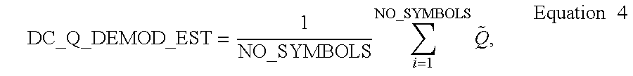
The output of IQ demodulator 34 may be measured for a set number of consecutive symbols NO_SYMBOLS. The two DC offset values DC_I_DEMOD_EST and DC_Q_DEMOD_EST of IQ demodulator 34 may be estimated as: DC_I _DEMOD _EST = 1 NO_SYMBOLS i = 1 NO_SYMBOLS I ~ Equation 3
Figure US06801581-20041005-M00001
DC_Q _DEMOD _EST = 1 NO_SYMBOLS i = 1 NO_SYMBOLS Q ~ , Equation 4
Figure US06801581-20041005-M00002
where Ĩ, {tilde over (Q)} are the real and imaginary parts, respectively, of the signal Vf produced by analog to digital converter 40 and NO_SYMBOLS is the number of symbols used for averaging. In one embodiment, NO_SYMBOLS=5.
These two values may be provided to summer 56 to generally cancel the DC offset of IQ demodulator 34.
Once the demodulator DC offset has been estimated, the modulator DC offset may be calculated by operating both transmission path 10 and feedback path 12. Transmission path 10 also includes a summer 60, which may subtract the modulator DC offset, DC_MOD_EST, from the signal produced by baseband modulator 20. To determine the modulator DC offset a zero input signal is provided (typically during a non-transmission slot) to baseband modulator 20. In addition, adaptive modulator estimator 52 may assign initial values, typically obtained from a factory calibration, to summer 60. The factory calibrated values may be far away from the true (and unknown) values due to thermal and frequency changes.
The resultant signal is transmitted by power amplifier 30 and may be received by feedback path 12, operating with logical switch 54 connecting analog to digital converter 40 to summer 56. The result is that summer 56 produces two signals eI and eQ which are the feedback path output with the DC offset from IQ demodulator generally removed. During non-transmission slots, the two signals may be given mathematically as:
eI=Ĩ-DC_I_DEMOD_EST,  Equation 5
eQ={tilde over (Q)}-DC_Q_DEMOD_EST,  Equation 6
where Ĩ, {tilde over (Q)} are defined hereinabove.
When determining the DC offset of IQ modulator 28, a logical switch 58 may provide the two signals eI and eQ to adaptive modulator estimator 52, which then operates to minimize the signals eI 2 and eQ 2.
At the end of each symbol period, adaptive modulator estimator 52 may compute (block 306 of FIG. 3):
DC_I_MOD_Cnew=DC_I_MOD_ColdI Re{erot I},  Equation 7
for the I channel and
DC_Q_MOD_Cnew=DC_Q_MOD_ColdQ Im{erot Q},  Equation 8
for the Q channel, where μIQ are the step sizes which control the rate of adaptation, 0 ≦μI≦1, 0≦μQ≦1 and erot I and erot Q are rotated errors given hereinbelow by Equation 9. DC_I_MOD_Cold and DC_Q_MOD_Cold are the previous values of offset estimation and initially may be the factory calibrated values.
Alternatively to using the steepest descent iteration method (implemented in Equation 7 and Equation 8), other iteration methods as are known from optimization theory, such as the conjugate gradient equation and the quasi-Newton equation, may be used to minimize the signals eI 2 and eQ 2. In some embodiments of the invention, the selected iteration method is chosen as a tradeoff between the processing power of the transmitter and the required convergence speed of the output of adaptive estimator 52. If fast convergence is required and the transmitter has a relatively high processing power level, a fast convergence method that requires dense computation (e.g., the quasi-Newton method) may be used. If, however, low processing power utilization is more important than fast convergence, simpler methods, such as the steepest descent method, may be used.
There is often a phase rotation {circumflex over (φ)}path along the path from the output of digital to analog converter 24 in transmission path 10 to the input to analog to digital converter 40 in feedback path 12. This phase rotation can be estimated (block 302 of FIG. 3) as described hereinbelow with respect to Equation 10 and then used to rotate (block 304 of FIG. 3) the errors eI and eQ according to:
erot I=eIe−j{circumflex over (φ)} path
erot Q=eQe−j{circumflex over (φ)} path   Equation 9
The phase {circumflex over (φ)}path is measured in the first transmission slot when data is transmitted. The angle θbip of the baseband input signal is measured, per symbol, as is the angle θout of each symbol of the signal Vf after analog to digital converter 40. The angle is defined as the angle in the complex plane of value Ĩ+j{tilde over (Q)}.
The phase {circumflex over (φ)}path is the average value of the difference in the angles. Thus:
{circumflex over (φ)}path=avg(θ out−θbip)  Equation 10
During regular operation, logical switches 54 and 58 are typically closed and the previously estimated DC offset values may be utilized in summers 56 and 60. Thus, feedback path 12 produces signals with minimal, if any, demodulator DC offset and the transmitted signal may have the modulator DC offset removed.
If desired, and particularly during long transmission periods, the DC offset estimators 50 and 52 can be operated again. To do so, the data of the next non-transmission slot is used. The DC offset estimators 50 and 52 are then operated on this data.
Reference is now made to FIG. 2, which illustrates a further embodiment of the invention implemented in a transmitter having a predistorter. Elements, which are similar to those of FIG. 1, have similar reference numerals.
FIG. 2 shows transmission path 10, feedback path 12, a predistorter 14 and DC offset estimator 16. The transmission path 10 generally comprises some or all of the following elements: baseband modulator 20, a finite impulse response (FIR) filter 22, digital to analog (D/A) converter 24, an analog filter 26, IQ modulator 28 and power amplifier 30. FIR filter 22 shapes the baseband signal as desired. Analog filter 26 filters the analog signal as necessary.
Feedback path 12 comprises some or all of the following elements: attenuator 32, IQ demodulator 34, a filter 36 and analog to digital (A/D) converter 40. Filter 36 limits any noise to the bandwidth of the demodulated signal.
Predistorter 14 comprises a predistorter (PD) lookup table (LUT) 42 and a PD LUT trainer 44. Pre-distorter 14 compensates for the non-linearity of power amplifier 30 and changes the signals entering power amplifier 30 such that the transmitted signals have substantially linear amplification (rather than the non-linear amplification, which occurs without the predistortion). Since the distortion changes due to temperature, aging and other characteristics of power amplifier 30, the predistortion values are updated by PD LUT trainer 44, based on feedback received from the output of power amplifier 30.
During regular transmission, PD LUT 42 predistorts the signal from baseband modulator 20 in order to compensate for the distortion produced by power amplifier 30. To do so, the output of PD LUT 42 is multiplied with the output of baseband modulator by multipliers 46 in transmission path 10. PD LUT trainer 44 regularly updates the values of PD LUT 42 based on data received along feedback path 12.
During regular operation, logical switches 54 and 58 are typically closed and any previously estimated DC offset values may be utilized in summers 56 and 60. Thus, PD LUT trainer 44 may receive signals with minimal, if any, demodulator DC offset and the transmitted signal may be both predistorted and may have the modulator DC offset removed.
DC offset estimator 16 operates as described hereinabove. Specifically, it operates during non-transmission slots and PD LUT 42 is disabled by indicating to multipliers 46 to pass the output of baseband modulator 20 rather than multiplying it by the output of PD LUT 42.
The methods and apparatus disclosed herein have been described without reference to specific hardware or software. Rather, the methods and apparatus have been described in a manner sufficient to enable persons of ordinary skill in the art to readily adapt commercially available hardware and software as may be needed to reduce any of the embodiments of the present invention to practice without undue experimentation and using conventional techniques.
It will be appreciated by persons skilled in the art that the present invention is not limited by what has been particularly shown and described herein above. Rather the scope of the invention is defined by the claims that follow:

Claims (18)

What is claimed is:
1. A method for reducing a DC offset in a transmitter, the transmitter having a transmission path with an IQ modulator and a feedback path with an IQ demodulator, the method comprising:
providing a predetermined signal to the input of said IQ modulator and transmitting said signal; estimating a DC offset of said IQ demodulator from a received version of said transmitted signal;
adaptively estimating a DC offset of said IQ modulator at least partially from said demodulator DC offset;
subtracting said estimated demodulator DC offset from said feedback path; and
subtracting said estimated modulator DC offset from said transmission path,
wherein said estimating said demodulator DC offset comprises averaging a received signal along said feedback path,
and wherein adaptively estimating said modulator DC offset comprises generating a difference signal between said received signal and said estimated demodulator DC offset and subtracting a modified rotated version of said difference signal from a previous value of said modulator DC offset.
2. A method according to claim 1 and wherein estimating said demodulator DC offset and adaptively estimating said modulator DC offset occur during non-transmission slots.
3. A method according to claim 2 and wherein said non-transmission slots are non-transmission slots of regular transmission.
4. A method according to claim 1 wherein adaptively estimating said modulator DC offset comprises estimating a phase rotation of said transmission and feedback paths and modifying said difference signal with said phase rotation.
5. A transmitter comprising:
a transmission path having an IQ modulator and a first summer;
a feedback path having an IQ demodulator and a second summer;
a demodulator DC offset estimator to average a received signal along said feedback path and to estimate a DC offset of said IQ demodulator;
an adaptive modulator DC offset estimator to estimate a DC offset of said IQ modulator at least partially from said demodulator DC offset,
wherein said second summer is to subtract said estimated demodulator DC offset from said feedback path,
wherein said first summer is to subtract said estimated modulator DC offset from said transmission path, and
wherein said adaptive modulator DC offset estimator is to generate a difference signal between said received signal and said demodulator DC offset and to subtract a modified rotated version of said difference signal from a previous value of said modulator DC offset.
6. A transmitter according to claim 5 and wherein said demodulator DC offset estimator and said adaptive modulator DC offset estimator are to operate during non-transmission slots.
7. A transmitter according to claim 6 and wherein said non-transmission slots are non-transmission slots of regular transmission.
8. A transmitter according to claim 5 wherein said adaptive modulator DC offset estimator is to modify said difference signal with a phase rotation of said transmission and feedback paths.
9. A transmitter according to claim 5 which forms part of a base station.
10. A transmitter according to claim 5 which forms part of a mobile communication unit.
11. A DC offset reducer comprising:
a transmission path having an IQ modulator and a first summer;
a feedback path having an IQ demodulator and a second summer;
a demodulator DC offset estimator to average a received signal along said feedback path and to estimate a DC offset of said IQ demodulator;
an adaptive modulator DC offset estimator to estimate a DC offset of said IQ modulator at least partially from said demodulator DC offset,
wherein said second summer is to subtract said estimated demodulator DC offset from said feedback path,
wherein said first summer is to subtract said estimated modulator DC offset from said transmission path, and
wherein said adaptive modulator DC offset estimator is to generate a difference signal between said received signal and said demodulator DC offset and to subtract a modified rotated version of said difference signal from a previous value of said modulator DC offset.
12. A DC offset reducer according to claim 11 and wherein said demodulator DC offset estimator and said adaptive modulator DC offset estimator are to operate during non-transmission slots.
13. A DC offset reducer according to claim 12 and wherein said non-transmission slots are non-transmission slots of regular transmission.
14. A DC offset reducer according to claim 11 wherein said adaptive modulator DC offset estimator is to modify said difference signal with a phase rotation of said transmission and feedback paths.
15. An integrated circuit (IC) having a transmitter, the transmitter comprising:
a transmission path having an IQ modulator and a first summer;
a feedback path having an IQ demodulator and a second summer;
a demodulator DC offset estimator to average a received signal along said feedback path and to estimate a DC offset of said IQ demodulator;
an adaptive modulator DC offset estimator to estimate a DC offset of said IQ modulator at least partially from said demodulator DC offset,
wherein said second summer is to subtract said estimated demodulator DC offset from said feedback path,
wherein said first summer is to subtract said estimated modulator DC offset from said transmission path, and
wherein said adaptive modulator DC offset estimator is to generate a difference signal between said received signal and said demodulator DC offset and to subtract a modified rotated version of said difference signal from a previous value of said modulator DC offset.
16. An IC according to claim 15 and wherein said demodulator DC offset estimator and said adaptive modulator DC offset estimator are to operate during non-transmission slots.
17. An IC according to claim 16 and wherein said non-transmission slots are non-transmission slots of regular transmission.
18. An IC according to claim 15 wherein said adaptive modulator DC offset estimator is to modify said difference signal with a phase rotation of said transmission and feedback paths.
US09/661,127 2000-09-13 2000-09-13 DC offset cancellation Expired - Fee Related US6801581B1 (en)

Priority Applications (2)

Application Number Priority Date Filing Date Title
US09/661,127 US6801581B1 (en) 2000-09-13 2000-09-13 DC offset cancellation
US10/924,996 US20050025255A1 (en) 2000-09-13 2004-08-25 DC offset cancellation

Applications Claiming Priority (1)

Application Number Priority Date Filing Date Title
US09/661,127 US6801581B1 (en) 2000-09-13 2000-09-13 DC offset cancellation

Related Child Applications (1)

Application Number Title Priority Date Filing Date
US10/924,996 Continuation US20050025255A1 (en) 2000-09-13 2004-08-25 DC offset cancellation

Publications (1)

Publication Number Publication Date
US6801581B1 true US6801581B1 (en) 2004-10-05

Family

ID=33030227

Family Applications (2)

Application Number Title Priority Date Filing Date
US09/661,127 Expired - Fee Related US6801581B1 (en) 2000-09-13 2000-09-13 DC offset cancellation
US10/924,996 Abandoned US20050025255A1 (en) 2000-09-13 2004-08-25 DC offset cancellation

Family Applications After (1)

Application Number Title Priority Date Filing Date
US10/924,996 Abandoned US20050025255A1 (en) 2000-09-13 2004-08-25 DC offset cancellation

Country Status (1)

Country Link
US (2) US6801581B1 (en)

Cited By (20)

* Cited by examiner, † Cited by third party
Publication number Priority date Publication date Assignee Title
US20030081701A1 (en) * 2001-10-26 2003-05-01 Kobby Pick Metric correction for multi user detection, for long codes DS-CDMA
US20040203542A1 (en) * 2002-06-04 2004-10-14 Jae-Hyun Seo Pre-distortion apparatus and method for recovering nonlinear distortion of high power amplifier
US20050018788A1 (en) * 2003-07-24 2005-01-27 Sumit Talwalkar Method and apparatus for RF carrier suppression
US20050058105A1 (en) * 2003-09-17 2005-03-17 Lg Electronics Inc. Apparatus and method for removing transmission DC offset from a mobile terminal transmission signal
US20050084043A1 (en) * 2003-10-16 2005-04-21 Baoguo Yang Adaptive multi-step combined DC offset compensation for edge 8-PSK
US20060183454A1 (en) * 2005-02-14 2006-08-17 Intelleflex Corporation Adaptive coherent RFID reader carrier cancellation
US7177366B1 (en) * 2001-09-06 2007-02-13 The Board Of Trustees Of The Leland Stanford Junior University Automatic phase alignment for high-bandwidth cartesian-feedback power amplifiers
US20070237259A1 (en) * 2006-04-07 2007-10-11 Hon Hai Precision Industry Co., Ltd. Circuit for canceling dc offset in a communication system
US20070291863A1 (en) * 2003-07-25 2007-12-20 Zarbana Digital Fund Llc Digital branch calibrator for an rf transmitter
US20080243047A1 (en) * 2007-03-27 2008-10-02 Babaev Eilaz P Ultrasound wound care device
US7653147B2 (en) * 2005-08-17 2010-01-26 Intel Corporation Transmitter control
US20100039158A1 (en) * 2008-08-12 2010-02-18 Fujitsu Limited Offset correction device and method
US20100118999A1 (en) * 2008-11-07 2010-05-13 Nec Electronics Corporation Communication apparatus and offset canceling method
US7776231B2 (en) 2005-04-21 2010-08-17 Anji Microelectronics (Shanghai) Co., Ltd. Chemical mechanical polishing slurries, their applications and method of use thereof
WO2011006016A1 (en) * 2009-07-08 2011-01-13 Qualcomm Incorporated Spur cancellation in a digital baseband transmit signal using cancelling tones
US20120133412A1 (en) * 2010-11-30 2012-05-31 Infineon Technologies Ag Square Wave Signal Component Cancellation
US8615204B2 (en) 2011-08-26 2013-12-24 Qualcomm Incorporated Adaptive interference cancellation for transmitter distortion calibration in multi-antenna transmitters
US8755756B1 (en) 2009-04-29 2014-06-17 Qualcomm Incorporated Active cancellation of interference in a wireless communication system
EP2770632A1 (en) * 2013-02-22 2014-08-27 Tektronix, Inc. Measurement of DC offsets in IQ modulators
CN104052699A (en) * 2013-03-14 2014-09-17 亚德诺半导体技术公司 Dc Bias Estimation Of A Radio Frequency Mixer

Families Citing this family (3)

* Cited by examiner, † Cited by third party
Publication number Priority date Publication date Assignee Title
US8522370B2 (en) * 2008-08-08 2013-09-03 S. C. Johnson & Son, Inc. Fluid dispenser
US8412132B2 (en) * 2008-08-21 2013-04-02 Freescale Semiconductor, Inc. Techniques for adaptive predistortion direct current offset correction in a transmitter
US8442150B1 (en) 2012-02-24 2013-05-14 National Instruments Corporation Measurement of transmitter impairments using offset local oscillators

Citations (9)

* Cited by examiner, † Cited by third party
Publication number Priority date Publication date Assignee Title
JPS647969A (en) * 1987-06-29 1989-01-11 Ueki Kokan Shokai Kk Device for producing coated steel deck or the like
US4878029A (en) * 1988-12-05 1989-10-31 General Electric Company Complex digital sampling converter for demodulator
US5870668A (en) * 1995-08-18 1999-02-09 Fujitsu Limited Amplifier having distortion compensation and base station for radio communication using the same
US6018650A (en) 1996-12-18 2000-01-25 Aironet Wireless Communications, Inc. Cellular communication devices with automated power level adjust
US6035004A (en) * 1995-11-02 2000-03-07 Mitsubishi Denki Kabushiki Kaisha Digital radio receiver
US6294952B1 (en) * 1999-05-24 2001-09-25 Advantest Corporation Quadrature demodulator quadrature demodulation method and recording medium
US20020018531A1 (en) * 1999-03-26 2002-02-14 Mika Ratto Correction of DC-offset of I/Q modulator
US6504884B1 (en) * 1999-05-12 2003-01-07 Analog Devices, Inc. Method for correcting DC offsets in a receiver
US6606359B1 (en) * 2000-07-26 2003-08-12 Motorola, Inc Area-optimum rapid acquisition cellular multi-protocol digital DC offset correction scheme

Family Cites Families (4)

* Cited by examiner, † Cited by third party
Publication number Priority date Publication date Assignee Title
US5761259A (en) * 1996-05-24 1998-06-02 International Business Machines Corporation Apparatus, method and article of manufacture for carrier frequency compensation in a FM radio
US5751114A (en) * 1996-05-24 1998-05-12 International Business Machines Corporation Apparatus, method and article of manufacture for carrier frequency compensation in a FM radio transmitter
US6421398B1 (en) * 2000-01-28 2002-07-16 Alcatel Canada Inc. Modulation system having on-line IQ calibration
US6741662B1 (en) * 2000-04-17 2004-05-25 Intel Corporation Transmitter linearization using fast predistortion

Patent Citations (9)

* Cited by examiner, † Cited by third party
Publication number Priority date Publication date Assignee Title
JPS647969A (en) * 1987-06-29 1989-01-11 Ueki Kokan Shokai Kk Device for producing coated steel deck or the like
US4878029A (en) * 1988-12-05 1989-10-31 General Electric Company Complex digital sampling converter for demodulator
US5870668A (en) * 1995-08-18 1999-02-09 Fujitsu Limited Amplifier having distortion compensation and base station for radio communication using the same
US6035004A (en) * 1995-11-02 2000-03-07 Mitsubishi Denki Kabushiki Kaisha Digital radio receiver
US6018650A (en) 1996-12-18 2000-01-25 Aironet Wireless Communications, Inc. Cellular communication devices with automated power level adjust
US20020018531A1 (en) * 1999-03-26 2002-02-14 Mika Ratto Correction of DC-offset of I/Q modulator
US6504884B1 (en) * 1999-05-12 2003-01-07 Analog Devices, Inc. Method for correcting DC offsets in a receiver
US6294952B1 (en) * 1999-05-24 2001-09-25 Advantest Corporation Quadrature demodulator quadrature demodulation method and recording medium
US6606359B1 (en) * 2000-07-26 2003-08-12 Motorola, Inc Area-optimum rapid acquisition cellular multi-protocol digital DC offset correction scheme

Non-Patent Citations (7)

* Cited by examiner, † Cited by third party
Title
Cavers, J.K., "New Methods for Adaption of Quadrature Modulators and Demodulators Amplifier LInearization Circuits", IEEE Trans. On Vehicular Technology, vol. 46, No. 3, Aug. 1997.
Cavers, J.K., "the Effect of Quadrature Modulator and Demodulator Errors on Adaptive Digital Predistorters for Amplifier Linearization", IEEE Trans. On Vehicular Technology, vol. 46, No. 2, May 1997.
Lohtia, P.A., Goud, P.A., Englefield, C.G., "An Adaptive Digital Technique for Compensation for Analog Quadrature Modulator/Demodulator Impairments", Wireless 94.
Matsuka Akihiko et al, Mar. 24, 1998, Derwent Publication No JP410079693A, Abstract only.* *
Sundstrom, L., Faulkner, M., and Johansson, M., "Quantization Analysis and Design of a Digital Predistortion Linearizer for RF Power Amplifiers", IEEE Trans. On Vehicular Technology, vol. 45, No. 4, Nov. 1996.
Sundstrom, L., Faulkner, M., Johansson, M., "Effects of REconstruction Filters in digital Predistortion Linearizers for RF Power Amplifiers", IEEE Trans. On Vehicular Technology, vol. 44, No. 1, Feb. 1995.
Wright, A.S., and Durtler, W.G., "Experimental Performance of an Adaptive Digital Linearized Power Amplifier", IEEE Trans. On Vehicular Technology, vol. 41, Nov. 1992.

Cited By (40)

* Cited by examiner, † Cited by third party
Publication number Priority date Publication date Assignee Title
US7177366B1 (en) * 2001-09-06 2007-02-13 The Board Of Trustees Of The Leland Stanford Junior University Automatic phase alignment for high-bandwidth cartesian-feedback power amplifiers
US20030081701A1 (en) * 2001-10-26 2003-05-01 Kobby Pick Metric correction for multi user detection, for long codes DS-CDMA
US7450631B2 (en) 2001-10-26 2008-11-11 Intel Corporation Metric correction for multi user detection, for long codes DS-CDMA
US7068980B2 (en) * 2002-06-04 2006-06-27 Electronics And Telecommunications Research Institute Pre-distortion apparatus and method for recovering nonlinear distortion of high power amplifier
US20040203542A1 (en) * 2002-06-04 2004-10-14 Jae-Hyun Seo Pre-distortion apparatus and method for recovering nonlinear distortion of high power amplifier
US7412006B2 (en) * 2003-07-24 2008-08-12 Freescale Semiconductor, Inc. Method and apparatus for RF carrier feedthrough suppression
US20050018788A1 (en) * 2003-07-24 2005-01-27 Sumit Talwalkar Method and apparatus for RF carrier suppression
US7522672B2 (en) * 2003-07-25 2009-04-21 Aryan Saed Digital branch calibrator for an RF transmitter
US8179993B2 (en) 2003-07-25 2012-05-15 Zarbana Digital Fund Llc Digital branch calibrator for an RF transmitter
US20070291863A1 (en) * 2003-07-25 2007-12-20 Zarbana Digital Fund Llc Digital branch calibrator for an rf transmitter
US20090279639A1 (en) * 2003-07-25 2009-11-12 Aryan Saed Digital branch calibrator for an rf transmitter
US20050058105A1 (en) * 2003-09-17 2005-03-17 Lg Electronics Inc. Apparatus and method for removing transmission DC offset from a mobile terminal transmission signal
US7457379B2 (en) * 2003-10-16 2008-11-25 Broadcom Corporation Adaptive multi-step combined DC offset compensation for EDGE 8-PSK
US20050084043A1 (en) * 2003-10-16 2005-04-21 Baoguo Yang Adaptive multi-step combined DC offset compensation for edge 8-PSK
US7526266B2 (en) 2005-02-14 2009-04-28 Intelleflex Corporation Adaptive coherent RFID reader carrier cancellation
US20060183454A1 (en) * 2005-02-14 2006-08-17 Intelleflex Corporation Adaptive coherent RFID reader carrier cancellation
US7776231B2 (en) 2005-04-21 2010-08-17 Anji Microelectronics (Shanghai) Co., Ltd. Chemical mechanical polishing slurries, their applications and method of use thereof
US7653147B2 (en) * 2005-08-17 2010-01-26 Intel Corporation Transmitter control
US20070237259A1 (en) * 2006-04-07 2007-10-11 Hon Hai Precision Industry Co., Ltd. Circuit for canceling dc offset in a communication system
US7711065B2 (en) 2006-04-07 2010-05-04 Hon Hai Precision Industry Co., Ltd. Circuit for canceling DC offset in a communication system
US20080243047A1 (en) * 2007-03-27 2008-10-02 Babaev Eilaz P Ultrasound wound care device
US7911254B2 (en) * 2008-08-12 2011-03-22 Fujitsu Limited Offset correction device and method
US20100039158A1 (en) * 2008-08-12 2010-02-18 Fujitsu Limited Offset correction device and method
US20100118999A1 (en) * 2008-11-07 2010-05-13 Nec Electronics Corporation Communication apparatus and offset canceling method
US8320482B2 (en) * 2008-11-07 2012-11-27 Renesas Electronics Corporation Communication apparatus and offset canceling method
US8755756B1 (en) 2009-04-29 2014-06-17 Qualcomm Incorporated Active cancellation of interference in a wireless communication system
US20110007839A1 (en) * 2009-07-08 2011-01-13 Qualcomm Incorporated Spur cancellation in a digital baseband transmit signal using cancelling tones
WO2011006016A1 (en) * 2009-07-08 2011-01-13 Qualcomm Incorporated Spur cancellation in a digital baseband transmit signal using cancelling tones
US8331485B2 (en) 2009-07-08 2012-12-11 Qualcomm Incorporated Spur cancellation in a digital baseband transmit signal using cancelling tones
US20120133412A1 (en) * 2010-11-30 2012-05-31 Infineon Technologies Ag Square Wave Signal Component Cancellation
US8358164B2 (en) * 2010-11-30 2013-01-22 Infineon Technologies Ag Square wave signal component cancellation
US8615204B2 (en) 2011-08-26 2013-12-24 Qualcomm Incorporated Adaptive interference cancellation for transmitter distortion calibration in multi-antenna transmitters
EP2770632A1 (en) * 2013-02-22 2014-08-27 Tektronix, Inc. Measurement of DC offsets in IQ modulators
CN104022834A (en) * 2013-02-22 2014-09-03 特克特朗尼克公司 Measurement of DC offsets in IQ modulator
US9025648B2 (en) 2013-02-22 2015-05-05 Tektronix, Inc. Measurement of DC offsets in IQ modulators
CN104022834B (en) * 2013-02-22 2018-06-01 特克特朗尼克公司 The measurement that DC is deviated in I/Q modulator
CN104052699A (en) * 2013-03-14 2014-09-17 亚德诺半导体技术公司 Dc Bias Estimation Of A Radio Frequency Mixer
US20140269985A1 (en) * 2013-03-14 2014-09-18 Analog Devices Technology Dc bias estimation of a radio frequency mixer
EP2779553A3 (en) * 2013-03-14 2014-12-10 Analog Devices Technology DC bias estimation of a radio frequency mixer
CN104052699B (en) * 2013-03-14 2017-12-05 亚德诺半导体集团 The DC bias estimations of RF mixer

Also Published As

Publication number Publication date
US20050025255A1 (en) 2005-02-03

Similar Documents

Publication Publication Date Title
US6801581B1 (en) DC offset cancellation
US6771709B2 (en) System and method for direct transmitter self-calibration
CN1218475C (en) Adaptive linearization of power amplifiers
US8009765B2 (en) Digital polar transmitter
US8026762B2 (en) High efficiency transmitter for wireless communication
US6252912B1 (en) Adaptive predistortion system
KR100539874B1 (en) Method and apparatus for self-calibrating in a mobile transceiver
US7349490B2 (en) Additive digital predistortion system employing parallel path coordinate conversion
US7409007B1 (en) Method and apparatus for reducing adjacent channel power in wireless communication systems
US20030197558A1 (en) Adaptive predistortion system and a method of adaptively predistorting a signal
EP2575310B1 (en) Method and device for digital baseband predistortion
US8983408B2 (en) Method and system for estimating and compensating non-linear distortion in a transmitter using calibration
EP0881807A1 (en) Transmitter
JPH1032435A (en) Method for correcting nonlinearity of amplifier and radio transmitter using the method
JPH1013160A (en) Method for correcting nonlinearity of amplifier and radio transmitter using the method
US6898252B1 (en) IQ mismatch cancellation
US11115068B2 (en) Data-based pre-distortion for nonlinear power amplifier
JP2001507196A (en) Pre-adaptive distortion application method
US7248642B1 (en) Frequency-dependent phase pre-distortion for reducing spurious emissions in communication networks
US20090161778A1 (en) Transmitter and Carrier Leak Detection Method
US6498529B1 (en) Method and apparatus for calculating the predistortion function from a power amplifier
EP2954612B1 (en) Signal predistortion by addition of a correction term depending on a predefined constellation symbol, a transmission model and a target constellation symbol
US8437430B2 (en) Remote transmit IQ imbalance calibration and correction at multicarrier receivers
KR100315425B1 (en) Apparatus And Method For High Speed Adaptive Predistortion Using Lookup Table
Nuñez Perez et al. FPGA‐based system for effective IQ imbalance mitigation of RF power amplifiers

Legal Events

Date Code Title Description
AS Assignment

Owner name: D.S.P.C. TECHNOLOGIES LTD., ISRAEL

Free format text: ASSIGNMENT OF ASSIGNORS INTEREST;ASSIGNORS:FRANCOS, AMIR;BARAK, ILAN;YELLIN, DANIEL;REEL/FRAME:011495/0216

Effective date: 20010101

AS Assignment

Owner name: D.S.P.C. TECHNOLOGIES LTD., ISRAEL

Free format text: CHANGE OF ADDRESS;ASSIGNOR:D.S.P.C. TECHNOLOGIES LTD.;REEL/FRAME:012252/0590

Effective date: 20011031

AS Assignment

Owner name: INTEL CORPORATION, CALIFORNIA

Free format text: ASSIGNMENT OF ASSIGNORS INTEREST;ASSIGNOR:D.S.P.C. TECHNOLOGIES LTD.;REEL/FRAME:014047/0317

Effective date: 20030501

FEPP Fee payment procedure

Free format text: PAYER NUMBER DE-ASSIGNED (ORIGINAL EVENT CODE: RMPN); ENTITY STATUS OF PATENT OWNER: LARGE ENTITY

Free format text: PAYOR NUMBER ASSIGNED (ORIGINAL EVENT CODE: ASPN); ENTITY STATUS OF PATENT OWNER: LARGE ENTITY

FPAY Fee payment

Year of fee payment: 4

FPAY Fee payment

Year of fee payment: 8

REMI Maintenance fee reminder mailed
LAPS Lapse for failure to pay maintenance fees
STCH Information on status: patent discontinuation

Free format text: PATENT EXPIRED DUE TO NONPAYMENT OF MAINTENANCE FEES UNDER 37 CFR 1.362

FP Lapsed due to failure to pay maintenance fee

Effective date: 20161005