US6829286B1 - Resonant cavity enhanced VCSEL/waveguide grating coupler - Google Patents
Resonant cavity enhanced VCSEL/waveguide grating coupler Download PDFInfo
- Publication number
- US6829286B1 US6829286B1 US10/136,953 US13695302A US6829286B1 US 6829286 B1 US6829286 B1 US 6829286B1 US 13695302 A US13695302 A US 13695302A US 6829286 B1 US6829286 B1 US 6829286B1
- Authority
- US
- United States
- Prior art keywords
- waveguide
- mirror
- grating
- vcsel
- optical coupler
- Prior art date
- Legal status (The legal status is an assumption and is not a legal conclusion. Google has not performed a legal analysis and makes no representation as to the accuracy of the status listed.)
- Expired - Lifetime, expires
Links
Images


Classifications
-
- G—PHYSICS
- G02—OPTICS
- G02B—OPTICAL ELEMENTS, SYSTEMS OR APPARATUS
- G02B6/00—Light guides; Structural details of arrangements comprising light guides and other optical elements, e.g. couplings
- G02B6/24—Coupling light guides
- G02B6/42—Coupling light guides with opto-electronic elements
- G02B6/4201—Packages, e.g. shape, construction, internal or external details
- G02B6/4204—Packages, e.g. shape, construction, internal or external details the coupling comprising intermediate optical elements, e.g. lenses, holograms
- G02B6/4214—Packages, e.g. shape, construction, internal or external details the coupling comprising intermediate optical elements, e.g. lenses, holograms the intermediate optical element having redirecting reflective means, e.g. mirrors, prisms for deflecting the radiation from horizontal to down- or upward direction toward a device
-
- G—PHYSICS
- G02—OPTICS
- G02B—OPTICAL ELEMENTS, SYSTEMS OR APPARATUS
- G02B6/00—Light guides; Structural details of arrangements comprising light guides and other optical elements, e.g. couplings
- G02B6/24—Coupling light guides
- G02B6/26—Optical coupling means
- G02B6/34—Optical coupling means utilising prism or grating
-
- H—ELECTRICITY
- H01—ELECTRIC ELEMENTS
- H01S—DEVICES USING THE PROCESS OF LIGHT AMPLIFICATION BY STIMULATED EMISSION OF RADIATION [LASER] TO AMPLIFY OR GENERATE LIGHT; DEVICES USING STIMULATED EMISSION OF ELECTROMAGNETIC RADIATION IN WAVE RANGES OTHER THAN OPTICAL
- H01S5/00—Semiconductor lasers
- H01S5/10—Construction or shape of the optical resonator, e.g. extended or external cavity, coupled cavities, bent-guide, varying width, thickness or composition of the active region
- H01S5/1028—Coupling to elements in the cavity, e.g. coupling to waveguides adjacent the active region, e.g. forward coupled [DFC] structures
- H01S5/1032—Coupling to elements comprising an optical axis that is not aligned with the optical axis of the active region
-
- H—ELECTRICITY
- H01—ELECTRIC ELEMENTS
- H01S—DEVICES USING THE PROCESS OF LIGHT AMPLIFICATION BY STIMULATED EMISSION OF RADIATION [LASER] TO AMPLIFY OR GENERATE LIGHT; DEVICES USING STIMULATED EMISSION OF ELECTROMAGNETIC RADIATION IN WAVE RANGES OTHER THAN OPTICAL
- H01S5/00—Semiconductor lasers
- H01S5/40—Arrangement of two or more semiconductor lasers, not provided for in groups H01S5/02 - H01S5/30
- H01S5/4025—Array arrangements, e.g. constituted by discrete laser diodes or laser bar
- H01S5/4031—Edge-emitting structures
- H01S5/4062—Edge-emitting structures with an external cavity or using internal filters, e.g. Talbot filters
-
- H—ELECTRICITY
- H01—ELECTRIC ELEMENTS
- H01S—DEVICES USING THE PROCESS OF LIGHT AMPLIFICATION BY STIMULATED EMISSION OF RADIATION [LASER] TO AMPLIFY OR GENERATE LIGHT; DEVICES USING STIMULATED EMISSION OF ELECTROMAGNETIC RADIATION IN WAVE RANGES OTHER THAN OPTICAL
- H01S5/00—Semiconductor lasers
- H01S5/40—Arrangement of two or more semiconductor lasers, not provided for in groups H01S5/02 - H01S5/30
- H01S5/42—Arrays of surface emitting lasers
- H01S5/423—Arrays of surface emitting lasers having a vertical cavity
-
- H—ELECTRICITY
- H01—ELECTRIC ELEMENTS
- H01S—DEVICES USING THE PROCESS OF LIGHT AMPLIFICATION BY STIMULATED EMISSION OF RADIATION [LASER] TO AMPLIFY OR GENERATE LIGHT; DEVICES USING STIMULATED EMISSION OF ELECTROMAGNETIC RADIATION IN WAVE RANGES OTHER THAN OPTICAL
- H01S5/00—Semiconductor lasers
- H01S5/02—Structural details or components not essential to laser action
- H01S5/026—Monolithically integrated components, e.g. waveguides, monitoring photo-detectors, drivers
-
- H—ELECTRICITY
- H01—ELECTRIC ELEMENTS
- H01S—DEVICES USING THE PROCESS OF LIGHT AMPLIFICATION BY STIMULATED EMISSION OF RADIATION [LASER] TO AMPLIFY OR GENERATE LIGHT; DEVICES USING STIMULATED EMISSION OF ELECTROMAGNETIC RADIATION IN WAVE RANGES OTHER THAN OPTICAL
- H01S5/00—Semiconductor lasers
- H01S5/10—Construction or shape of the optical resonator, e.g. extended or external cavity, coupled cavities, bent-guide, varying width, thickness or composition of the active region
- H01S5/14—External cavity lasers
- H01S5/141—External cavity lasers using a wavelength selective device, e.g. a grating or etalon
-
- H—ELECTRICITY
- H01—ELECTRIC ELEMENTS
- H01S—DEVICES USING THE PROCESS OF LIGHT AMPLIFICATION BY STIMULATED EMISSION OF RADIATION [LASER] TO AMPLIFY OR GENERATE LIGHT; DEVICES USING STIMULATED EMISSION OF ELECTROMAGNETIC RADIATION IN WAVE RANGES OTHER THAN OPTICAL
- H01S5/00—Semiconductor lasers
- H01S5/10—Construction or shape of the optical resonator, e.g. extended or external cavity, coupled cavities, bent-guide, varying width, thickness or composition of the active region
- H01S5/18—Surface-emitting [SE] lasers, e.g. having both horizontal and vertical cavities
- H01S5/183—Surface-emitting [SE] lasers, e.g. having both horizontal and vertical cavities having only vertical cavities, e.g. vertical cavity surface-emitting lasers [VCSEL]
- H01S5/18308—Surface-emitting [SE] lasers, e.g. having both horizontal and vertical cavities having only vertical cavities, e.g. vertical cavity surface-emitting lasers [VCSEL] having a special structure for lateral current or light confinement
- H01S5/18311—Surface-emitting [SE] lasers, e.g. having both horizontal and vertical cavities having only vertical cavities, e.g. vertical cavity surface-emitting lasers [VCSEL] having a special structure for lateral current or light confinement using selective oxidation
-
- H—ELECTRICITY
- H01—ELECTRIC ELEMENTS
- H01S—DEVICES USING THE PROCESS OF LIGHT AMPLIFICATION BY STIMULATED EMISSION OF RADIATION [LASER] TO AMPLIFY OR GENERATE LIGHT; DEVICES USING STIMULATED EMISSION OF ELECTROMAGNETIC RADIATION IN WAVE RANGES OTHER THAN OPTICAL
- H01S5/00—Semiconductor lasers
- H01S5/10—Construction or shape of the optical resonator, e.g. extended or external cavity, coupled cavities, bent-guide, varying width, thickness or composition of the active region
- H01S5/18—Surface-emitting [SE] lasers, e.g. having both horizontal and vertical cavities
- H01S5/183—Surface-emitting [SE] lasers, e.g. having both horizontal and vertical cavities having only vertical cavities, e.g. vertical cavity surface-emitting lasers [VCSEL]
- H01S5/18361—Structure of the reflectors, e.g. hybrid mirrors
- H01S5/1838—Reflector bonded by wafer fusion or by an intermediate compound
-
- H—ELECTRICITY
- H01—ELECTRIC ELEMENTS
- H01S—DEVICES USING THE PROCESS OF LIGHT AMPLIFICATION BY STIMULATED EMISSION OF RADIATION [LASER] TO AMPLIFY OR GENERATE LIGHT; DEVICES USING STIMULATED EMISSION OF ELECTROMAGNETIC RADIATION IN WAVE RANGES OTHER THAN OPTICAL
- H01S5/00—Semiconductor lasers
- H01S5/40—Arrangement of two or more semiconductor lasers, not provided for in groups H01S5/02 - H01S5/30
- H01S5/4025—Array arrangements, e.g. constituted by discrete laser diodes or laser bar
- H01S5/4031—Edge-emitting structures
- H01S5/4068—Edge-emitting structures with lateral coupling by axially offset or by merging waveguides, e.g. Y-couplers
Definitions
- the present invention is directed generally to coupling light from one location to another, and more particularly to a resonant cavity enhanced waveguide grating coupler.
- Coupling of light from one point to another or one location to another particularly in optical transmission of information, production of high power coherent light, pump sources for laser, and the like.
- the challenges presented are illustrated, for example, in the context of developing high power vertical cavity surface emitting lasers (VCSELs).
- VCSELs vertical cavity surface emitting lasers
- the elements of one or two dimensional VCSEL arrays should be phase-locked.
- the light from each individual VCSEL is coherent, the phase and frequencies (or wavelengths) of the light from each VCSEL are slightly different and therefore uncorrelated.
- the on-axis power in the far-field is ⁇ NP.
- the on-axis power in the far-field is N 2 P and the width of the radiation pattern is reduced by ⁇ 1/N.
- the present invention which includes a waveguide and surface normal gratings.
- an optical coupler comprising first and second mirrors, wherein the first mirror is positioned with respect to the second mirror so that a resonant cavity is defined between them, a waveguide structure positioned in the resonant cavity and including a surface-normal grating structure, and wherein a thickness of the resonant cavity is selected so that a phase matching condition is satisfied for resonance in the resonant cavity.
- At least one of the first and second mirrors is formed from a structure in an optoelectronic device.
- at least one of the first and second mirrors is formed from a semiconductor layer.
- At least one of the first and second mirrors is formed as a semiconductor distributed bragg reflector.
- at least one of the first and second mirrors is formed as a dielectric distributed bragg reflector.
- At least one of the first and second mirrors can be a mirror in a vertical cavity surface emitting laser (VCSEL) structure. Also, at least one of the first and second mirrors is a mirror in a photodetector structure, in a different embodiment.
- VCSEL vertical cavity surface emitting laser
- the first and second mirrors and waveguide structure can be formed in a hybrid structure, or a monolithic structure.
- the surface-normal grating structure is shaped so that first order modes of light It incident upon the surface-normal grating structure are coupled into the waveguide while zero-order modes are reflected out into the resonant cavity and reflected by the mirror.
- Coupling into and out of a waveguide using a grating is a simple method to transfer free space data to waveguides in optoelectronic integrated circuits (OEICs).
- Waveguide gratings can perform a large variety of functions such as reflection, filtering, deflection, and input/output coupling.
- a periodically modulated grating can perform holographic-wavefront conversion.
- the grating converts a waveguide mode into a radiation mode, or vice versa.
- Surface-normal grating couplers direct light perpendicularly into and out of the waveguide. The combination of the waveguide and surface normal grating couplers permits arrays of VCSELs to be used to create an optical source with high right angle mode output power.
- Arrays of VCSELs can then be used as high-power light sources for use in a variety of military and commercial applications, such as free-space optical communications, on-chip/chip-to-chip communications, RF photonics, laser radar, and optical pump sources for solid-state and fiber lasers.
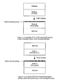
- FIG. 1 is an illustration of a resonant cavity enhance (RCE) waveguide grating coupler in accordance with the present invention.
- RCE resonant cavity enhance
- FIG. 2 is an illustration of a hybrid RCE VCSEL/waveguide grating coupler in accordance with the present invention.
- FIG. 3 is an illustration of a hybrid RCE photodetector/waveguide grating coupler in accordance with the present invention.
- FIG. 4 is a schematic of a monolithic RCE waveguide grating coupler in which a mirror M 1 is monolithically integrated with a waveguide structure and a mirror M 2 on a semiconductor substrate in accordance with the present invention.
- FIG. 5 is a simplified monolithic RCE VCSEL/waveguide grating coupler which can be realized using an epitaxial regrowth technique in accordance with the present invention.
- FIG. 6 is a simplified monolithic RCE photodetector/waveguide grating coupler which can be realized using an epitaxial regrowth technique in accordance with the present invention.
- FIG. 7 is a simplified monolithic RCE VCSEL/waveguide grating coupler which can be realized using a wafer bonding technique in accordance with the present invention.
- FIG. 8 is a simplified monolithic RCE photodetector/waveguide grating coupler which can be realized using a wafer bonding technique in accordance with the present invention.
- FIG. 9 is a simplified hybrid system with VCSELs coupled through a surface normal grating into a waveguide in accordance with the present invention.
- FIG. 10 is a schematic drawing of a waveguide structure where the VCSEL light is coupled through the surface-normal second-order grating coupler and showing the phase-matching condition in accordance with the present invention.
- FIG. 11 is a schematic diagram of a three-layer waveguide structure in accordance with the present invention.
- FIG. 12 is a diagram illustrating a mathematical model showing the coupling of a single VCSEL output into a waveguide through the surface normal grating in accordance with the present invention.
- FIGS. 13A and 13B are graphs of the calculated output power coupled into the waveguide as a function of diffraction efficiency in accordance with the present invention.
- FIG. 14 is a schematic diagram of a two VCSEL/waveguide system in accordance with the present invention.
- FIGS. 15A and 15B are graphs of the calculated waveguide output for a two VCSEL/waveguide grating system as a function of diffraction efficiency in accordance with the present invention.
- FIG. 16 is a schematic diagram of an N VCSEL/waveguide grating structure in accordance with the present invention.
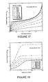
- FIG. 17 is a graph of the calculated waveguide output for an N VCSEL/waveguide grating system as a function of diffraction efficiency for different number of VCSELs in accordance with the present invention.
- FIG. 18 is a graph of the coupled output power for an N VCSEL/waveguide grating system as a function of diffraction efficiencies in accordance with the present invention.
- FIG. 19 is a graph of the power coupling efficiency for an N VCSEL/waveguide grating system as a function of the number of VCSELs for different diffraction efficiencies in accordance with the present invention.
- FIG. 20 is a graph of the coupled output power for an N VCSEL/waveguide grating system as a function of the substrate mirror reflectivity for a different number of VCSELs in accordance with the present invention.
- FIG. 21 is a graph of the calculated waveguide output for an N VCSEL/waveguide grating system as a function of diffraction efficiency for different number of VCSELs in accordance with the present invention.
- FIG. 22 is a graph of the coupled output power for an N VCSEL/waveguide grating system as a function of different diffraction efficiencies in accordance with the present invention.
- FIG. 23 is a graph of the power coupling efficiency for an N VCSEL/waveguide grating system as a function of the number of VCSELs for different diffraction efficiencies in accordance with the present invention.
- FIG. 24 is a diagram of a 2D array of a VCSEL/waveguide grating structure in accordance with the present invention.
- FIG. 25 is a diagram of an ion implanted VCSEL in accordance with the present invention.
- FIG. 26 is a diagram of an oxide confined VCSEL in accordance with the present invention.
- FIG. 27 is a diagram of an 8 ⁇ 8 VCSEL array in accordance with the present invention.
- FIG. 28 is a diagram of voltages and currents applied to VCSELs in accordance with the present invention.
- FIG. 29 is a diagram of peak wavelengths of a 1 ⁇ 5 VCSEL array in accordance with the present invention.
- FIG. 30 is a diagram of mean wavelengths of a 1 ⁇ 5 VCSEL array in accordance with the present invention.
- FIG. 31 is a diagram of an epitaxial structure for a single mode waveguide in accordance with the present invention.
- FIG. 32 is a diagram of an epitaxial structure for a multimode waveguide in accordance with the present invention.
- FIG. 33 is a diagram of a series of grating pitches in accordance with the present invention.
- FIG. 34 is a diagram of a cascade VCSEL array coupled into an optical waveguide in accordance with the present invention.
- FIG. 35 is a diagram of a VSCEL array on a smart pixel substrate with a common driver and equal path length delays to the VSCEL in accordance with the present invention.
- FIG. 36 is a diagram of an EDGA pump module in accordance with the present invention.
- FIG. 37 is a diagram of the EDFA pump amplifier characteristics in accordance with the present invention.
- FIG. 38 is a diagram of a parallel array for an optical pump in accordance with the present invention.
- FIG. 39 is a diagram of a one-point-to-many points fan-out utilizing VCSEL/waveguide interconnects in accordance with the present invention.
- FIG. 40 is a diagram of a many-points-to-one point fan-out utilizing VCSEL/waveguide interconnects and smart pixel devices in accordance with the present invention.
- FIG. 41A is a diagram of a global waveguide optical interconnects for many-points-to-many points fan-out/fan-in utilizing VCSEL/waveguide interconnects and smart pixel devices in accordance with the present invention.
- FIG. 41B is a schematic diagram of an equivalent logic circuit demonstrating feedback of the global waveguide optical interconnects of FIG. 41 A.
- FIG. 42 is a diagram of a processor/memory interconnect via parallel optical waveguide bus configured as a crossbar switch in accordance with the present invention.
- FIG. 43 is a diagram of a smart pixel set utilized in a parallel crossbar in accordance with the present invention.
- a resonant cavity enhanced (RCE) waveguide grating coupler includes a surface-normal waveguide grating inserted into a Fabry-Perot cavity (FIG. 1 ).
- the Fabry-Perot cavity has two mirrors and, between them, a cavity which contains a waveguide grating layer.
- the mirror can be either a semiconductor layer, a semiconductor distributed bragg reflector (DBR) or a dielectric DBR.
- DBR distributed bragg reflector
- Semiconductor DBR mirrors can be a part of an optoelectronic device, particularly a vertical cavity surface emitting laser (VCSEL) or a photodetector.
- the thickness of the cavity should be designed in such a way that a phase matching condition is satisfied for resonance.
- Light can be coupled into/out of an optical fiber through the surface-normal waveguide grating.
- a coupling efficiency into the waveguide layer can be greatly enhanced due to the large increase of the resonant optical field introduced by the Fabry-Perot cavity.
- Two approaches can be used to realize the RCE waveguide grating coupler: hybrid and monolithic.
- FIG. 2 shows an example of a simplified hybrid RCE VCSEL/waveguide grating coupler which comprises a VCSEL and a waveguide structure which contains a waveguide layer with a surface-normal grating in combination with a mirror M 2 .
- the VCSEL serves as a mirror M 1 as well as a light source. Collimating optics can be used to capture light from the VCSEL more efficiently and direct it into the waveguide.
- the output of the VCSEL is coupled through a grating into a waveguide for edge emission from the waveguide structure.
- waveguide coupling can be greatly enhanced by multiple reflections between the mirror M 2 and the mirror M 1 .
- the multiple reflections cause the light to be continually directed back into the waveguide.
- the waveguide grating coupler then redirects this vertical light horizontally into the waveguide.
- the waveguide coupled output power can be considerably increased.
- FIG. 3 shows a simplified hybrid RCE photodetector/waveguide grating coupler which comprises a photodetector and a waveguide structure which contains a waveguide layer with a surface-normal grating in combination with a mirror M 2 .
- the photodetector can be served as a mirror M 1 .
- the photodetector can be either a non-resonant photodetector or an RCE photodetector.
- the waveguide grating coupler functions as a beam router which directs the horizontal light into the vertical light.
- FIG. 4 shows a schematic of a monolithic RCE waveguide grating coupler in which a mirror M 1 is monolithically integrated with a waveguide structure and a mirror M 2 on a semiconductor substrate.
- the waveguide structure can be a part of M 1 and inserted into any positions in M 1 .
- a monolithic RCE waveguide grating coupler has several advantages over the hybrid counterpart, including no need for external optics, easy alignment, and a simple package. This monolithic structure can be implemented using two technical approaches: epitaxial regrowth technique and wafer bonding technique.
- FIG. 5 shows a simplified monolithic RCE VCSEL/waveguide grating coupler which can be realized using an epitaxial regrowth technique.
- the surface-normal grating is first fabricated into the waveguide layer using an etching technique. Then, an epitaxial regrowth is performed to grow the VCSEL structure using an epitaxial growth machine.
- FIG. 6 shows a simplified monolithic RCE photodetector/waveguide grating coupler which can be realized using an epitaxial regrowth technique.
- the surface-normal grating is first fabricated into the waveguide layer using an etching technique. Then, an epitaxial regrowth is performed to grow the photodetector structure.
- FIG. 7 shows a simplified monolithic RCE VCSEL/waveguide grating coupler which can be realized using a wafer bonding technique.
- Two epitaxial wafers are separately grown on semiconductor substrates using an epitaxial growth machine, a wafer A and a wafer B.
- the wafer A contains a waveguide structure and M 2 while the wafer B contains a VCSEL (M 1 ).
- the surface-normal grating is first fabricated on the wafer A using an etching technique. Then, wafer bonding is performed to fuse the wafers A and B.
- the wafer-fused monolithic RCE VCSEL/waveguide grating coupler has air/semiconductor gratings.
- These gratings are embedded between the wafers A and B.
- the efficiency of the grating can be enhanced by enclosing air in its grooves during the fabrication process.
- the air/semiconductor gratings have a large coupling efficiency due to the large difference between the refractive index of air and that of a semiconductor.
- FIG. 8 shows a simplified monolithic RCE photodetector/waveguide grating coupler which can be realized using a wafer bonding technique.
- Two epitaxial wafers are separately grown on semiconductor substrates using an epitaxial growth machine, a wafer C and a wafer D.
- the wafer C contains a waveguide structure and M 2 while the wafer D contains a photodetector (M 1 ).
- the surface-normal grating is first fabricated on the wafer C using an etching technique. Then, wafer bonding is performed to fuse the wafers C and D.
- the wafer-fused monolithic RCE photodetector/waveguide grating coupler has air/semiconductor gratings. These gratings are embedded between the wafers C and D. The efficiency of the grating can be enhanced by enclosing air in its grooves during the fabrication process.
- the monolithic RCE VCSEL/WGC structure offers a method to monolithically integrate active VCSELs and passive waveguide devices.
- This structure has the inherently bi-directional nature which enables simultaneous coupling into two opposite directions in the waveguide.
- the bi-directional coupling capability can further increase the flexibility in the design of complex optical devices and circuits, allowing entirely new hardware architectures to be implemented.
- These bi-directional devices can be utilized in applications such as optical communications, optical signal processing, and optical networks. Some of the specific applications are optical transceivers; distributed crossbar switches; coherent high power sources; multiplexers and demultiplexers
- a hybrid VCSEL/waveguide architecture is provided by which, for example, coherent high-power light sources can be achieved.
- the hybrid VCSEL/waveguide structure comprises a VCSEL array and a single waveguide with a periodic grating in combination with a substrate reflector (FIG. 9 ).
- the waveguide is attached to the VCSEL array through mechanical spacers.
- Optical coupling between the array elements is provided by the grating coupled waveguide.
- An optical waveguide with a series of gratings allows the distribution and coupling of light into and out of individual VCSEL elements, thereby locking each element into a coherent, single frequency array mode.
- waveguide coupling can be greatly enhanced by multiple reflections between the substrate reflector and the top VCSEL mirror.
- the multiple reflections cause the light to be continually directed back into the waveguide.
- the waveguide grating coupler then redirects this vertical light horizontally into the waveguide.
- the distribution waveguide method can provide phase locking by controlling a precise amount of coupling between array elements independent of the element size and element spacing.
- the grating coupled waveguide provides a linear array of elements which can be extended into a 2D array with the integration of a waveguide coupler.
- the waveguide grating coupler is a key component of the VCSEL/waveguide grating system.
- the performance of the system depends largely on the grating coupler. It is of considerable interest to develop predictions of the efficiency of the diffraction process in terms of the waveguide and grating parameters.
- the coupling efficiency of a grating coupler is dependent on several parameters such as the grating depth, the index modulation of the grating, and the type of grating.
- FIG. 10 shows a schematic drawing of a waveguide structure where the VCSEL light is coupled through the surface-normal second-order grating coupler.
- the phase matching condition dictates that the difference between the wavevector of the incident beam and the wavevector of the diffracted beam has to be conserved through the wavevector of the surface grating.
- FIG. 11 A typical three-layer waveguide is shown in FIG. 11 .
- Layer 2 is the waveguide core and layers 1 and 3 are the cladding layers.
- n i is the refractive index of layer i.
- Two different waveguide structures were initially examined; asymmetric and symmetric.
- an asymmetric waveguide structure was chosen for this program. It was found from the design process that a symmetric waveguide has several disadvantages over an asymmetric waveguide structure.
- the waveguide were designed for both singlemode and multimode operations.
- the number of modes in the waveguide is dependent on the thickness of the waveguide core layer as well as the index difference between the waveguide and cladding layers.
- FIG. 12 is a mathematical model showing the coupling of a single VCSEL output into a waveguide through the surface normal grating. Collimated light from the VCSEL is emitted in transverse electromagnetic mode TEM 00 (A in ). This is depicted by the arrows in FIG. 12 .
- the surface normal grating is designed to separate first-order modes and couple these modes into the waveguide.
- the zero-order mode (undiffracted light) is reflected back by the reflection from the mirror on the waveguide. Through a reflections of R 1 and R 2 the zero-order mode sustains the amplitude of the first-order modes. This is achieved through superposition.
- R 1 and R 2 are the reflectivities of the VCSEL and the substrate reflector;
- a R1 is normalized to the incident beam A in ; is the diffraction efficiency of the surface-normal grating coupler.
- Equation (1) is derived by assuming that the diffraction efficiency from the waveguide is the same as that from the VCSEL and there is no reflection at the grating coupler. It is also assumed that the zero-order mode reflected from the substrate mirror is in phase with the component diffracted into the waveguide. The phase matching condition is determined by the thickness of the cladding layers below the waveguide. In addition, the absorption and scattering losses in the waveguide are assumed to be minimal.
- the output power coupled into the ⁇ z direction A 1L can be calculated in a similar way to A R1 .
- a L1 A R1 , since, in this calculation, a symmetric grating is assumed.
- the coupling processes are also symmetric. Therefore, light from the VCSEL is coupled by the surface normal grating coupler and is split into two different directions at the same time with the same magnitude.
- FIGS. 13 (A) and 13 (B) shows the calculated output power coupled into the waveguide as a function of the diffraction efficiency for different values of R 1 .
- R 2 0.35
- the normalized output power approximately exhibits a linear dependence on the diffraction efficiency for all values of R 1 .
- a reflectivity of R 2 0.35 is typical of a GaAs-air interface.
- the coupling characteristics can be substantially changed if a substrate mirror is used.
- the coupled output power can be increased by incorporating a highly reflective mirror into the backside of the waveguide structure. This can be accomplished using a simple gold mirror or a semiconductor (dielectric) mirror such as an epitaxially grown distributed bragg reflector (DBR).
- DBR distributed bragg reflector
- FIG. 13 (B) shows the calculated output power for a large R 2 of 0.95.
- the coupled output exhibits a nonlinear dependence on ⁇ in which the output becomes saturated rapidly with ⁇ .
- the effect of the substrate reflector on the coupled output power becomes smaller as ⁇ increases.
- a two element VCSEL/waveguide grating structure is shown in FIG. 14 .
- Light from each source (VCSEL 1 and VCSEL 2 ) is coupled by the grating coupler and diffracted equally to the left and to the right of each grating (Grating 1 and Grating 2 ).
- the waveguide allows the light to travel in either direction.
- the first-order diffracted light can be transmitted through the grating and reflected back from the grating.
- the light can be also coupled back into the VCSELs. It is estimated that only a small amount of optical power is required to achieve phase-locking in the longitudinal direction (z).
- the light inputs to the gratings from the VCSELs are defined by A in1 and A in2 .
- the light output on the right (left) side of the waveguide is designated as A R2 (A L2 ). It includes the following optical contributions: light from VCSEL 2 through Grating 2 , light from VCSEL 1 through Gratings 1 and 2 ; and light from VCSELs 1 and 2 which experiences multiple reflections due to the in-plane reflections of the gratings.
- the in-plane reflectivity from the waveguide grating is designated as R c .
- the waveguide-coupled output power is calculated by summing all the contributions described above and is given by:
- a L2 (1 +M 2 S ) A in1 +M 2 M 1 A in2 (4)
- M 1 n 2 ⁇ 1 + R 2 ⁇ ( 1 - ⁇ ) 1 - R 1 ⁇ R 2 ⁇ ( 1 - ⁇ ) 2 ( 5 )
- M 2 K 1 - S 2 ( 6 )
- M 1 is the output power for a single VCSEL/waveguide structure and M 2 is a coupling coefficient due to multiple reflections between Gratings 1 and 2 .
- K and S are the transmission and reflection coefficients of the grating, respectively. It is assumed in this calculation that all the gratings are symmetric and their properties are the same.
- the output for A 2R has been calculated for various R 1 values for two different R 2 of 0.35 (a) and 0.95 (b).
- the light output is plotted versus the diffraction efficiency of the waveguide grating.
- a in1 is equal to A in2 .
- the values have been normalized to A in1 .
- the in-plane grating reflectivity, R c is assumed to be zero.
- the output power becomes approximately twice larger in magnitude than that of the single cell. This is because of an increase in the number of VCSELs.
- the coupling efficiency is also increased with an increase in VCSEL reflectivity. It is expected that when R 1 increases, the amount of reflected light from the VCSELs will be enhanced, giving rise to the increase in the coupled power.
- FIG. 8 shows an N VCSEL/waveguide grating structure.
- the light inputs to the gratings from the VCSELs are defined by A in1 , A in2 , and A inN .
- the light output on the right (left) side of the waveguide Is designated as A RN (A LN ).
- each VCSEL makes different contributions to the output power depending on the position of the VCSEL. For example, the VCSEL N makes the most contribution to A RN , while VCSEL 1 makes the least contribution to A RN . This is because light output from VCSEL 1 should travel through N gratings to reach the right end of the waveguide, while light from VCSEL N encounters only one grating.
- the transmitted light output is decreased due to in-plane reflections at the grating as well as radiation losses into the VCSEL and the substrate mirror. If there is no in-plane reflection from the grating and the reflectivities of the VCSEL and substrate mirror are unity, then there will be no loss in the waveguide grating system. Hence, the light outputs from all the VCSELs will be diffracted into the waveguide and travel in the waveguide without loss.
- a L ⁇ ⁇ N ⁇ ( 1 + M N ⁇ ⁇ M N ⁇ ( 1 + M N ⁇ b N -
- b i is the reflection coefficient of the waveguide with i gratings.
- M i is the coupling coefficient due to multiple reflections In an i waveguide grating system.
- K and S which are given in equations 7 and 8, are the transmission and reflection coefficients of a single grating, respectively.
- the waveguide coupled output power is plotted as a function of diffraction efficiency of the grating coupler.
- the coupled output power is increased with the number of VCSELs as well as with the diffraction efficiency. A larger number of VCSELs produce more diffracted light coupled into the waveguide and hence increase the out-put power.
- the coupled output is saturated to a small value with a small number of VCSELs.
- the output is saturated with only 10 VCSELs for ⁇ of > ⁇ 0.5.
- Increasing the number of VCSELs beyond 10 will not cause the output power to be further increased.
- the number of VCSELs or gratings is increased, the more loss is introduced into the system. Since the reflectivities of the VCSELs and the substrate mirror are not unity, there are always radiation losses into the air via the waveguide substrate and the VCSEL.
- the coupled output power A RN is replotted as a function of the number of VCSELs for different diffraction efficiencies of 0.1, 0.2, 0.4, 0.6, 0.8, and 1.
- the figure shows clearly the effect of the number of VCSELs on the output power.
- the output is rapidly saturated for a small number of VCSELs.
- a RN has a maximum value of ⁇ 2.8 for ⁇ 1.
- the power coupling efficiency of a VCSEL/waveguide grating system is defined as the waveguide coupled output power divided by the number of VCSELs. This can be used as a figure-of-merit to determine an optimum number of VCSELs in an array in order to produce a coherent high power laser output.
- FIG. 20 shows the coupled output power as a function of the substrate mirror reflectivity R 2 .
- R 2 the substrate mirror reflectivity
- FIG. 21 shows the output power coupled into the waveguide versus the diffraction efficiency of the grating for different number of VCSELs.
- the number of VCSELs is varied from 1 to 1000.
- the output power is increased with the number of VCSELs.
- the coupled output power is replotted versus the number of VCSELs for different diffraction efficiencies.
- the number of VCSELs has a pronounced effect on the coupling efficiency.
- the output is saturated with increasing the number of VCSELs. For a small ⁇ , the output is slowly saturated for a large number of VCSELs. However, as ⁇ increases, the number of VCSELs limiting the output becomes smaller.
- the coupled output exhibits a monotonous decrease with ⁇ for a large number of VCSELs.
- waveguide coupling can be enhanced by using a highly reflective mirror on the backside of the waveguide structure, the power coupling efficiency is still relatively low.
- One possible method is to put a highly reflective coating on one of the facets of the waveguide structure, which is not the output port.
- the idea is to use a highly reflective mirror to reflect back A LN to the waveguide.
- the output power coupled into +z direction can be enhanced by multiple reflections between the facet reflector and the waveguide gratings.
- the waveguide structure should be designed in such a way that the reflected light from the facet of the waveguide is added in phase with the guided modes in the waveguide.
- the coupled output power can be also enhanced by using two dimensional (2D) arrays of the VCSEL/waveguide structure, as shown in FIG. 24 .
- the planar waveguides for each row of VCSELs are connected together using a waveguide coupler. From the calculations, there is an optimum number of VCSELs that can be used to obtain a reasonable coupling efficiency. By increasing the array size, the output power can be greatly increased.
- a hybrid waveguide structure was integrated with a diffractive optical interconnect element or DOIE array and a 1 ⁇ 5 VCSEL array.
- the single element coupling demonstration was crucial in determining the optimal waveguide structure.
- a series of waveguide structures were fabricated with various periods and grating depths. Grating depths and spacings were based on a spectral evaluation and characterization of candidate set of VCSELs.
- An 8 ⁇ 8 VCSEL ion implanted VCSEL array was used in the evaluation with a 1 ⁇ 5 array of elements selected.
- the spectral analysis was carried out at Opticomp Corporation (OCC) on selected VCSELs and the results were then forwarded to SMU where a candidate set of epitaxial gratings were determined and fabricated. Gratings were then bracketed around the mean average wavelength.
- OCC Opticomp Corporation
- FIG. 25 shows 850 nm VCSEL structures which were developed by OCC for optoelectronic integrated circuit (OEIC) integration. Arrays have been fabricated in 8 ⁇ 8 and 16 ⁇ 16 configurations. The lasers were processed from a GaAs/AlGaAs p-i-n distributed Bragg reflector (DBR) structure, which was grown by using metal organic chemical vapor deposition (MOCVD).
- DBR distributed Bragg reflector
- MOCVD metal organic chemical vapor deposition
- the ion implanted VCSEL shown in FIG. 25 is a gain guided top-surface emitting device in which current confinement and electrical isolation of adjacent lasers is accomplished through hydrogen ion implantation.
- the oxide confined VCSEL structure (FIG. 26) uses flip-chip bonding to CMOS and subsequent substrate removal.
- the oxide confined VCSELs offer improved operational characteristics such as lower threshold or “turn on” currents and improved conversion efficiency. Although either device could be incorporated into the VCSEL/waveguide ad structure, a top emit-ting ion implanted VCSEL array was used for this demonstration.
- FIG. 28 shows the voltages of (VddMOD) used to drive the eight channel CMOS driver chips and the output drive current recorded operate a single VCSEL.
- FIGS. 29 and 30, summarize the spectral results of the five element VCSEL array evaluation.
- FIG. 29 shows a comparison of the peak wavelengths at various voltages. The voltages refer to the VddMOD applied to the eight channel CMOS driver chips.
- FIG. 30 shows a comparison of the mean wavelengths at various voltages.
- FIGS. 31 and 32 show the epitaxial structures.
- the epitaxial wafers are based on GaAs and AlGaAs semiconductor materials.
- An AlAs layer was first grown on a GaAs substrate. This AlAs layer serves as an etch-stop layer for the removal of the GaAs substrate.
- a thin GaAs layer was then grown and followed by an AlGaAs cladding layer.
- an AlGaAs waveguide core layer was grown. The thickness of the waveguide core was determined to be 0.5 ⁇ m and 8 ⁇ m for single mode and multi mode waveguides, respectively.
- the GaAs epitaxial samples were cleaved into 10 samples.
- the samples were cleaned with acetone and rinsed with methanol and DI water and dried.
- the samples were then spin coated with a Shipley resist at 4500 rpm for 20 seconds and then softbaked for 90 seconds.
- the holographic grating fabrication process at SMU which was modified from a previous sequence [Evans, Carson, Hammer, Butler, Grating Surface Emitting Lasers, Academic Press, New York, 1993; Heflinger, Kirk, Corero, and Evans, Proceeding of SPIE, Vol. 269, 1981] comprises splitting a laser beam into two beams which are recombined at an angle, producing an interference pattern which is recorded in the photoresist.
- the light source used in this holographic process is an ultraviolet argon ion laser with an emission wavelength of 351.1 nm.
- the beam is spatially filtered, expanded using 4-inch diameter optics, and then collimated. By adjusting the angle between the two beams, the period of the resulting standing wave can be adjusted from ⁇ 180 nm to >1000 nm.
- the wafer containing the photoresist is developed and the resulting photoresist grating pattern is replicated in the wafer surface using a dry etching process using a reactive ion etcher.
- the dry etching process does not limit the orientation of the device relative to crystal planes. It has several advantages over other processing techniques such as uniformity, control, and the capability for increased grating depths.
- the samples were placed in an oxygen plasma ash to remove any remaining photoresist.
- the samples were lapped and edges cleaved for ease of evaluation and coupling.
- Gratings were fabricated with the following periods as shown in FIG. 33 .
- the pitch was varied every 20 ⁇ , in order to bracket the optimal performance given a specific ⁇ of 44.8 nm.
- a testbed was fabricated to evaluate the waveguide grating structures.
- the testbed used a specialized PCB board which contains integrated laser drivers and filtering components to drive VCSEL arrays.
- the output radiation was then collimated with an diffractive optical interconnect element (DOIE).
- DOIE diffractive optical interconnect element
- the DOIE was mounted to a carrier and mounted to a multiaxial positioner.
- the collimated laser beam was incident on the waveguide.
- the VCSELs were set to 5.0 V.
- a 400 ⁇ microscope was placed to examine the cleaved edge of the waveguide.
- the beam was incident on the waveguide ⁇ 1 mm from the edge of the waveguide.
- a CCD camera was placed so as to resolve the microscope image. All gratings were taken at the same power levels and angular positions.
- the waveguides were attached to a glass slide and mounted. Incident VCSEL radiation was positioned at 500 mm, 1.5 ⁇ m, and 2.5 mm. An image was then recorded at each distance for evaluation.
- the grating OSU-884-10 shows the best waveguide results.
- the grating periods were not optimized for the OCC VCSEL.
- the output VCSEL light is faintly visible to the CCD camera in both photos.
- Gratings OSU-884-1:9 show markedly poor results due to the fact that not enough light could be coupled.
- the OSU-884-10 grating demonstrates that waveguiding is being accomplished through the displayed increase in intensity.
- the OSU-884-10 grating shows the corner of the waveguide, while the OSU-884-8 grating shows the middle of the waveguide.
- the OSU884-10 grating also shows scattering at the cleaved interface due to surface imperfections.
- the OSU-884-9 grating shows a series of the same grating with a different beam position. All of the samples were tested at the same positions and VCSEL power levels. It was determined from these results that another set of waveguides should be generated with grating pitches 100 ⁇ beyond the grating spacing of 2493.2 ⁇ . This will further confirm which gratings are optimally suited for the OCC VCSEL array.
- a well known approach to increase the performance in an RF photonic link is to use the method of cascading lasers [C. Cox, “RF Photonic Testbed and Direct Modulation of Cascaded Laser,” MURI on RF Photonic Materials and Devices, Review, Oct. 22, 1998] when implementing direct modulation.
- Laser relative intensity noise (RIN) dominates over other laser noises and must be minimized.
- the method of cascading lasers increases the signal power for a given current linearly while adding noise sources orthogonally.
- the gain in an optical link is determined by several parameters:
- ⁇ L is the RF-to-optical conversion efficiency (laser slope efficiency); L is the total loss in the fiber link; and ⁇ D is the optical-to-RF conversion efficiency (detector efficiency) at the receiver end.
- the noise figure is proportional to 1/ ⁇ L 2 .
- a method which utilizes a VCSEL cascade coupled to a waveguide as a hybrid structure (FIG. 34 ).
- the system decreases RIN and increases power.
- the VCSEL array outputs are collimated with a DOIE lens and coupled through surface-normal grating couplers to generate the optical source.
- the VCSELs are flip-chip bonded to a silicon on sapphire (SOS) CMOS smart pixel array in order to drive the lasers at high speeds.
- the cascade VCSEL/waveguide may be coupled to a single mode fiber using V-groove methods for attachment
- FIG. 34 illustrates a Cascade VCSEL array coupled into an optical waveguide.
- SOS technology may currently be designed for 5 GHz applications. With future reductions in gate widths, 10 GHz applications can be expected.
- the power level at the optical output of the waveguide may ideally approach the sum of all VCSEL inputs. This is attractive for a number of applications which involve coupling multiple VCSEL sources into a single mode fiber.
- the application of free-space optical interconnect solutions for the coupling of single mode lasers into a single mode fiber is tenuous.
- the superposition of VCSEL emission sources utilizing optical waveguides appears attractive especially when coupling into a single mode fiber is required.
- FIG. 36 A schematic drawing of a complete EDFA pump module with the laser source is shown in FIG. 36.
- FIG. 37 A partial list of EDFA specifications is summarized in FIG. 37 [Private discussion: Dr. Steve Bashden, OptiGain, October, 1998].
- the 200 mW power levels are currently satisfied with single stripe edge-emission devices.
- Multiple VCSELs connected in parallel, in one or two dimensions as shown in FIG. 38, may potentially achieve similar or higher power levels.
- an array geometry of 10 ⁇ 10 VCSELs each having an output power of 2 mW could theoretically achieve 200 mW output into the fiber through the waveguide, assuming 100% coupling efficiency.
- the entire array would occupy a space 500 ⁇ m ⁇ 500 ⁇ m to achieve 200 mW.
- Initial calculations indicate that the hybrid waveguide configuration can achieve 65% coupling efficiency. This would require more power from each VCSEL ( ⁇ 3 mW) or an additional 30 VCSELs. Substantially higher power levels should be achievable out of the waveguide.
- Initial calculations indicate that the 1550 nm single-mode fiber (multimode at 978) has a capacity of 500 mW before undesired nonlinear effects become significant.
- ion implanted VCSELs demonstrate >1 ⁇ 10 6 hours mean time to failure (MTTF)[R. A. Morgan et al., “Reliability study of 850 nm VCSELs for data communications,” 34th Annual Proceedings of International Reliability Physics Symposium, pp. 203-10, 1996]. Should one or more VCSELs stop lasing, the decrease in output power is not significant. In fact, several devices would have to fail before the amplifier performance is degraded below the required specifications. This “slow” failure mode would not be considered catastrophic. Consequently, significant “down time” may be avoided and the pump laser replacement may be scheduled. Infant mortality and yield are also substantially improved thereby reducing cost.
- MTTF mean time to failure
- VCSELs have approximately a 3:1 decrease in thermal drift compared to stripe designs.
- VCSELs can be utilized as 980 nm pump sources for conventional EDFAs.
- the VCSEL/waveguide structure can be used in commercial applications which implement fan-out and fan-in architectures (FIGS. 39, 40 , 41 A, 41 B).
- fan-out Using a one-point-to-many-points architecture (fan-out), clock signals can be distributed on a single chip or between chips (FIG. 39 ).
- Logic NOR gates can be realized with the many-points-to-one-point architecture: fan-in (FIG. 40 ).
- fan-in and fan-out By combining fan-in and fan-out in the same waveguide a many-points-to-many-points architecture can be achieved (FIGS. 41 A & 41 B).
- This fan-in/fan-out represents a programmable gate array which can implement feedback.
- On-Chip Data Distribution e.g. Clock
- Chip-to-Chip Interconnect Fan-Out
- the many-point-to-one-point fan-in topology which is shown in FIG. 40, may in fact represent the next architectural evolution after the one-point-to-many-points configuration. This is referred to, for digital signals, as a “smart” interconnect. If the input signals or bits are represented in complementary notation, and the output is inverted, then the system is effectively an N-input AND gate by DeMorgan's Theorem [OptiComp patent” Global Interconnect Architecture for Optical Computer,” U.S. Pat. No. 5,297,068, 1994.; OptiComp patent “General Purpose Optical Computer, “U.S. Pat. No.
- Each processor/memory subsystem has a dedicated receiver and its own dedicated waveguide channel as shown in FIG. 43 . All waveguide channels cross over each processor/memory smart pixel chip. Each processor memory smart pixel chip has N-transmitter VCSELs, one for each waveguide channel except for the receive and the control channel. In this configuration, the controller can route the signal from any “transmit” processor/memory element to any “receive” processor/memory element. Note that none of the receivers fully utilize DeMorgan's Theorem due to the fact that there is only one signal on each channel at any time.
- the complete fan-in/fan-out system shown in FIGS. 41A & 41B, configures the crossbar to be able to become “controller free.”
- This architecture could be configured as a fully non-blocking gigabit Ethernet crossbar anarchy. Each channel senses every other channel and effectively waits for a “go” signal.
- Many other applications may be implemented with the global waveguide interconnect system, which is effectively a programmable gate array with feedback.
- Resonant cavity enhanced VCSEL/waveguide grating coupler was proposed to achieve coherent high-power light sources.
- the surface-normal grating is utilized to achieve the desired coupling light from the VCSEL into the waveguide.
- the waveguide structures were based on GaAs and AlGaAs semiconductor materials. They were designed for both singlemode and multi-mode operations at 850 nm.
- a mathematical model has been presented to describe diffraction into a waveguide from a normally incident light from the VCSEL. From the calculations, it was found that the coupling efficiency can be considerably enhanced by using a substrate mirror. The coupling efficiency has a pronounced dependence on the reflectivity of the substrate mirror. The substrate mirror redirects light emitted toward the substrate, thereby increasing the coupling into the waveguide. Therefore, the waveguide grating structure with a highly reflective mirror allows the use of low diffraction efficiency for large coupling efficiency of the VCSEL into the waveguide.
Landscapes
- Physics & Mathematics (AREA)
- General Physics & Mathematics (AREA)
- Optics & Photonics (AREA)
- Condensed Matter Physics & Semiconductors (AREA)
- Electromagnetism (AREA)
- Optical Integrated Circuits (AREA)
Abstract
Description


Claims (33)
Priority Applications (3)
| Application Number | Priority Date | Filing Date | Title |
|---|---|---|---|
| US10/136,953 US6829286B1 (en) | 2000-05-26 | 2002-05-01 | Resonant cavity enhanced VCSEL/waveguide grating coupler |
| US10/860,607 US7535944B1 (en) | 2000-05-26 | 2004-06-03 | Photonic crystal/waveguide coupler for VCSELS and photodetectors |
| US12/005,193 US7627018B1 (en) | 2000-05-26 | 2007-12-26 | Polarization control using diffraction gratings in VCSEL waveguide grating couplers |
Applications Claiming Priority (3)
| Application Number | Priority Date | Filing Date | Title |
|---|---|---|---|
| US20752500P | 2000-05-26 | 2000-05-26 | |
| US86771901A | 2001-05-29 | 2001-05-29 | |
| US10/136,953 US6829286B1 (en) | 2000-05-26 | 2002-05-01 | Resonant cavity enhanced VCSEL/waveguide grating coupler |
Related Parent Applications (1)
| Application Number | Title | Priority Date | Filing Date |
|---|---|---|---|
| US86771901A Continuation | 2000-05-26 | 2001-05-29 |
Related Child Applications (1)
| Application Number | Title | Priority Date | Filing Date |
|---|---|---|---|
| US10/860,607 Continuation-In-Part US7535944B1 (en) | 2000-05-26 | 2004-06-03 | Photonic crystal/waveguide coupler for VCSELS and photodetectors |
Publications (1)
| Publication Number | Publication Date |
|---|---|
| US6829286B1 true US6829286B1 (en) | 2004-12-07 |
Family
ID=33479173
Family Applications (1)
| Application Number | Title | Priority Date | Filing Date |
|---|---|---|---|
| US10/136,953 Expired - Lifetime US6829286B1 (en) | 2000-05-26 | 2002-05-01 | Resonant cavity enhanced VCSEL/waveguide grating coupler |
Country Status (1)
| Country | Link |
|---|---|
| US (1) | US6829286B1 (en) |
Cited By (57)
| Publication number | Priority date | Publication date | Assignee | Title |
|---|---|---|---|---|
| US20030223756A1 (en) * | 2002-06-04 | 2003-12-04 | Honeywell International Inc. | Optical transceiver |
| US20040071387A1 (en) * | 2002-07-31 | 2004-04-15 | Tony Mule | Back-side-of-die, through-wafer guided-wave optical clock distribution networks, method of fabrication thereof, and uses thereof |
| US20060245460A1 (en) * | 2005-04-29 | 2006-11-02 | Pavilion Integration Corporation | Vertical cavity surface emitting laser (VCSEL) arrays pumped solid-state lasers |
| US20070075265A1 (en) * | 2005-09-30 | 2007-04-05 | Virgin Islands Microsystems, Inc. | Coupled nano-resonating energy emitting structures |
| US20070104443A1 (en) * | 2005-10-21 | 2007-05-10 | Amr Helmy | Apparatus and methods for achieving phase-matching using a waveguide |
| US20070170370A1 (en) * | 2005-09-30 | 2007-07-26 | Virgin Islands Microsystems, Inc. | Structures and methods for coupling energy from an electromagnetic wave |
| US20070183717A1 (en) * | 2006-02-09 | 2007-08-09 | Virgin Islands Microsystems, Inc. | Method and structure for coupling two microcircuits |
| US7265439B1 (en) * | 1999-11-30 | 2007-09-04 | Avago Technologies Fiber Ip (Singapore) Pte. Ltd. | Low cost, high speed, high efficiency infrared transceiver |
| US20070217750A1 (en) * | 2006-03-14 | 2007-09-20 | International Business Machines Corporation | Interconnecting (mapping) a two-dimensional optoelectronic (OE) device array to a one-dimensional waveguide array |
| US20070259641A1 (en) * | 2006-05-05 | 2007-11-08 | Virgin Islands Microsystems, Inc. | Heterodyne receiver array using resonant structures |
| US20070256472A1 (en) * | 2006-05-05 | 2007-11-08 | Virgin Islands Microsystems, Inc. | SEM test apparatus |
| US7359589B2 (en) * | 2006-05-05 | 2008-04-15 | Virgin Islands Microsystems, Inc. | Coupling electromagnetic wave through microcircuit |
| AT504657B1 (en) * | 2007-07-13 | 2008-07-15 | Univ Linz | OPTOELECTRONIC COUPLER |
| US20080253423A1 (en) * | 2007-04-13 | 2008-10-16 | Commissariat A L'energie Atomique | Compact opto-electronic device including at least one surface emitting laser |
| US7443577B2 (en) | 2006-05-05 | 2008-10-28 | Virgin Islands Microsystems, Inc. | Reflecting filtering cover |
| US7442940B2 (en) | 2006-05-05 | 2008-10-28 | Virgin Island Microsystems, Inc. | Focal plane array incorporating ultra-small resonant structures |
| US7443358B2 (en) | 2006-02-28 | 2008-10-28 | Virgin Island Microsystems, Inc. | Integrated filter in antenna-based detector |
| US7450794B2 (en) | 2006-09-19 | 2008-11-11 | Virgin Islands Microsystems, Inc. | Microcircuit using electromagnetic wave routing |
| US7470920B2 (en) | 2006-01-05 | 2008-12-30 | Virgin Islands Microsystems, Inc. | Resonant structure-based display |
| US7476907B2 (en) | 2006-05-05 | 2009-01-13 | Virgin Island Microsystems, Inc. | Plated multi-faceted reflector |
| US7492868B2 (en) | 2006-04-26 | 2009-02-17 | Virgin Islands Microsystems, Inc. | Source of x-rays |
| US20090154868A1 (en) * | 2007-12-17 | 2009-06-18 | Electronics And Telecommunications Research Institute | Semiconductor opto-electronic integrated circuits and methods of forming the same |
| US7646991B2 (en) | 2006-04-26 | 2010-01-12 | Virgin Island Microsystems, Inc. | Selectable frequency EMR emitter |
| US7655934B2 (en) | 2006-06-28 | 2010-02-02 | Virgin Island Microsystems, Inc. | Data on light bulb |
| US7656094B2 (en) | 2006-05-05 | 2010-02-02 | Virgin Islands Microsystems, Inc. | Electron accelerator for ultra-small resonant structures |
| US7659513B2 (en) | 2006-12-20 | 2010-02-09 | Virgin Islands Microsystems, Inc. | Low terahertz source and detector |
| US7679067B2 (en) | 2006-05-26 | 2010-03-16 | Virgin Island Microsystems, Inc. | Receiver array using shared electron beam |
| US7710040B2 (en) | 2006-05-05 | 2010-05-04 | Virgin Islands Microsystems, Inc. | Single layer construction for ultra small devices |
| US7718977B2 (en) | 2006-05-05 | 2010-05-18 | Virgin Island Microsystems, Inc. | Stray charged particle removal device |
| US7723698B2 (en) | 2006-05-05 | 2010-05-25 | Virgin Islands Microsystems, Inc. | Top metal layer shield for ultra-small resonant structures |
| US7728397B2 (en) | 2006-05-05 | 2010-06-01 | Virgin Islands Microsystems, Inc. | Coupled nano-resonating energy emitting structures |
| US7728702B2 (en) | 2006-05-05 | 2010-06-01 | Virgin Islands Microsystems, Inc. | Shielding of integrated circuit package with high-permeability magnetic material |
| US7732786B2 (en) | 2006-05-05 | 2010-06-08 | Virgin Islands Microsystems, Inc. | Coupling energy in a plasmon wave to an electron beam |
| US7741934B2 (en) | 2006-05-05 | 2010-06-22 | Virgin Islands Microsystems, Inc. | Coupling a signal through a window |
| US7746532B2 (en) | 2006-05-05 | 2010-06-29 | Virgin Island Microsystems, Inc. | Electro-optical switching system and method |
| US7791053B2 (en) | 2007-10-10 | 2010-09-07 | Virgin Islands Microsystems, Inc. | Depressed anode with plasmon-enabled devices such as ultra-small resonant structures |
| US7791291B2 (en) | 2005-09-30 | 2010-09-07 | Virgin Islands Microsystems, Inc. | Diamond field emission tip and a method of formation |
| US7876793B2 (en) | 2006-04-26 | 2011-01-25 | Virgin Islands Microsystems, Inc. | Micro free electron laser (FEL) |
| US20110158278A1 (en) * | 2009-12-30 | 2011-06-30 | Koch Brian R | Hybrid silicon vertical cavity laser with in-plane coupling |
| US7986113B2 (en) | 2006-05-05 | 2011-07-26 | Virgin Islands Microsystems, Inc. | Selectable frequency light emitter |
| US7990336B2 (en) | 2007-06-19 | 2011-08-02 | Virgin Islands Microsystems, Inc. | Microwave coupled excitation of solid state resonant arrays |
| US8188431B2 (en) | 2006-05-05 | 2012-05-29 | Jonathan Gorrell | Integration of vacuum microelectronic device with integrated circuit |
| EP2535749A1 (en) * | 2011-06-17 | 2012-12-19 | Caliopa NV | Optical interposer |
| US8384042B2 (en) | 2006-01-05 | 2013-02-26 | Advanced Plasmonics, Inc. | Switching micro-resonant structures by modulating a beam of charged particles |
| EP2746828A1 (en) | 2012-12-19 | 2014-06-25 | Caliopa NV | Optical interposer |
| CN104011950A (en) * | 2012-01-18 | 2014-08-27 | 惠普发展公司,有限责任合伙企业 | High density laser optics |
| US9184562B2 (en) | 2009-02-11 | 2015-11-10 | Danmarks Tekniske Universitet | Hybrid vertical-cavity laser |
| CN106025793A (en) * | 2016-07-15 | 2016-10-12 | 厦门乾照光电股份有限公司 | Semiconductor laser with second resonant cavity |
| US20160301188A1 (en) * | 2013-10-29 | 2016-10-13 | Hewlett Packard Enterprise Development Lp | High contrast grating optoelectronics |
| US20170141533A1 (en) * | 2015-11-18 | 2017-05-18 | International Business Machines Corporation | Silicon photonic chip with integrated electro-optical component and lens element |
| US9853416B2 (en) | 2016-01-11 | 2017-12-26 | Alcatel-Lucent Usa Inc. | Multimode vertical-cavity surface-emitting laser |
| US20180138654A1 (en) * | 2016-11-16 | 2018-05-17 | Fanuc Corporation | Laser device |
| US10075257B2 (en) | 2016-01-11 | 2018-09-11 | Nokia Of America Corporation | Optical spatial division multiplexing usable at short reach |
| US10082684B2 (en) | 2014-01-24 | 2018-09-25 | Hewlett Packard Enterprise Development Lp | Optical modulation employing high contrast grating lens |
| US10193632B2 (en) | 2013-05-22 | 2019-01-29 | Hewlett Packard Enterprise Development Lp | Optical devices including a high contrast grating lens |
| FR3071326A1 (en) * | 2017-09-18 | 2019-03-22 | Robert Bosch Gmbh | INTEGRATED OPTICAL SYSTEM |
| US20210302673A1 (en) * | 2020-03-27 | 2021-09-30 | Enplas Corporation | Optical receptacle and optical module |
Citations (8)
| Publication number | Priority date | Publication date | Assignee | Title |
|---|---|---|---|---|
| US4674100A (en) * | 1983-10-06 | 1987-06-16 | Nec Corporation | Bistable optical device |
| US4743083A (en) * | 1985-12-30 | 1988-05-10 | Schimpe Robert M | Cylindrical diffraction grating couplers and distributed feedback resonators for guided wave devices |
| US5003550A (en) * | 1990-03-09 | 1991-03-26 | Spectra Diode Laboratories, Inc. | Integrated laser-amplifier with steerable beam |
| US5029297A (en) * | 1989-10-13 | 1991-07-02 | At&T Bell Laboratories | Optical amplifier-photodetector device |
| US5111467A (en) * | 1990-09-10 | 1992-05-05 | Tacan Corporation | Hybrid rugate filter assembly for temperature stabilized emission of grating coupled surface emitting lasers |
| US5771254A (en) * | 1996-01-25 | 1998-06-23 | Hewlett-Packard Company | Integrated controlled intensity laser-based light source |
| US5835517A (en) * | 1996-10-04 | 1998-11-10 | W. L. Gore & Associates, Inc. | WDM multiplexer-demultiplexer using Fabry-Perot filter array |
| US6055262A (en) * | 1997-06-11 | 2000-04-25 | Honeywell Inc. | Resonant reflector for improved optoelectronic device performance and enhanced applicability |
-
2002
- 2002-05-01 US US10/136,953 patent/US6829286B1/en not_active Expired - Lifetime
Patent Citations (8)
| Publication number | Priority date | Publication date | Assignee | Title |
|---|---|---|---|---|
| US4674100A (en) * | 1983-10-06 | 1987-06-16 | Nec Corporation | Bistable optical device |
| US4743083A (en) * | 1985-12-30 | 1988-05-10 | Schimpe Robert M | Cylindrical diffraction grating couplers and distributed feedback resonators for guided wave devices |
| US5029297A (en) * | 1989-10-13 | 1991-07-02 | At&T Bell Laboratories | Optical amplifier-photodetector device |
| US5003550A (en) * | 1990-03-09 | 1991-03-26 | Spectra Diode Laboratories, Inc. | Integrated laser-amplifier with steerable beam |
| US5111467A (en) * | 1990-09-10 | 1992-05-05 | Tacan Corporation | Hybrid rugate filter assembly for temperature stabilized emission of grating coupled surface emitting lasers |
| US5771254A (en) * | 1996-01-25 | 1998-06-23 | Hewlett-Packard Company | Integrated controlled intensity laser-based light source |
| US5835517A (en) * | 1996-10-04 | 1998-11-10 | W. L. Gore & Associates, Inc. | WDM multiplexer-demultiplexer using Fabry-Perot filter array |
| US6055262A (en) * | 1997-06-11 | 2000-04-25 | Honeywell Inc. | Resonant reflector for improved optoelectronic device performance and enhanced applicability |
Cited By (91)
| Publication number | Priority date | Publication date | Assignee | Title |
|---|---|---|---|---|
| US7265439B1 (en) * | 1999-11-30 | 2007-09-04 | Avago Technologies Fiber Ip (Singapore) Pte. Ltd. | Low cost, high speed, high efficiency infrared transceiver |
| US8340528B2 (en) * | 2002-06-04 | 2012-12-25 | Finisar Corporation | Optical transceiver |
| US7831152B2 (en) * | 2002-06-04 | 2010-11-09 | Finisar Corporation | Optical transceiver |
| US20030223756A1 (en) * | 2002-06-04 | 2003-12-04 | Honeywell International Inc. | Optical transceiver |
| US20110110669A1 (en) * | 2002-06-04 | 2011-05-12 | Finisar Corporation | Optical transciever |
| US20040071387A1 (en) * | 2002-07-31 | 2004-04-15 | Tony Mule | Back-side-of-die, through-wafer guided-wave optical clock distribution networks, method of fabrication thereof, and uses thereof |
| US7016569B2 (en) * | 2002-07-31 | 2006-03-21 | Georgia Tech Research Corporation | Back-side-of-die, through-wafer guided-wave optical clock distribution networks, method of fabrication thereof, and uses thereof |
| US7758739B2 (en) | 2004-08-13 | 2010-07-20 | Virgin Islands Microsystems, Inc. | Methods of producing structures for electron beam induced resonance using plating and/or etching |
| US20060245460A1 (en) * | 2005-04-29 | 2006-11-02 | Pavilion Integration Corporation | Vertical cavity surface emitting laser (VCSEL) arrays pumped solid-state lasers |
| US7430231B2 (en) * | 2005-04-29 | 2008-09-30 | Ningyi Luo | Vertical cavity surface emitting laser (VCSEL) arrays pumped solid-state lasers |
| US7361916B2 (en) | 2005-09-30 | 2008-04-22 | Virgin Islands Microsystems, Inc. | Coupled nano-resonating energy emitting structures |
| US7714513B2 (en) | 2005-09-30 | 2010-05-11 | Virgin Islands Microsystems, Inc. | Electron beam induced resonance |
| US20070170370A1 (en) * | 2005-09-30 | 2007-07-26 | Virgin Islands Microsystems, Inc. | Structures and methods for coupling energy from an electromagnetic wave |
| US20070075265A1 (en) * | 2005-09-30 | 2007-04-05 | Virgin Islands Microsystems, Inc. | Coupled nano-resonating energy emitting structures |
| US7791290B2 (en) | 2005-09-30 | 2010-09-07 | Virgin Islands Microsystems, Inc. | Ultra-small resonating charged particle beam modulator |
| US7791291B2 (en) | 2005-09-30 | 2010-09-07 | Virgin Islands Microsystems, Inc. | Diamond field emission tip and a method of formation |
| US7715677B2 (en) * | 2005-10-21 | 2010-05-11 | Amr Helmy | Apparatus and methods for achieving phase-matching using a waveguide |
| US20070104443A1 (en) * | 2005-10-21 | 2007-05-10 | Amr Helmy | Apparatus and methods for achieving phase-matching using a waveguide |
| US8384042B2 (en) | 2006-01-05 | 2013-02-26 | Advanced Plasmonics, Inc. | Switching micro-resonant structures by modulating a beam of charged particles |
| US7470920B2 (en) | 2006-01-05 | 2008-12-30 | Virgin Islands Microsystems, Inc. | Resonant structure-based display |
| US20070183717A1 (en) * | 2006-02-09 | 2007-08-09 | Virgin Islands Microsystems, Inc. | Method and structure for coupling two microcircuits |
| US7282776B2 (en) | 2006-02-09 | 2007-10-16 | Virgin Islands Microsystems, Inc. | Method and structure for coupling two microcircuits |
| US7443358B2 (en) | 2006-02-28 | 2008-10-28 | Virgin Island Microsystems, Inc. | Integrated filter in antenna-based detector |
| US7688274B2 (en) | 2006-02-28 | 2010-03-30 | Virgin Islands Microsystems, Inc. | Integrated filter in antenna-based detector |
| US20070217750A1 (en) * | 2006-03-14 | 2007-09-20 | International Business Machines Corporation | Interconnecting (mapping) a two-dimensional optoelectronic (OE) device array to a one-dimensional waveguide array |
| US7474815B2 (en) * | 2006-03-14 | 2009-01-06 | International Business Machines Corporation | Interconnecting (mapping) a two-dimensional optoelectronic (OE) device array to a one-dimensional waveguide array |
| US7876793B2 (en) | 2006-04-26 | 2011-01-25 | Virgin Islands Microsystems, Inc. | Micro free electron laser (FEL) |
| US7492868B2 (en) | 2006-04-26 | 2009-02-17 | Virgin Islands Microsystems, Inc. | Source of x-rays |
| US7646991B2 (en) | 2006-04-26 | 2010-01-12 | Virgin Island Microsystems, Inc. | Selectable frequency EMR emitter |
| US7732786B2 (en) | 2006-05-05 | 2010-06-08 | Virgin Islands Microsystems, Inc. | Coupling energy in a plasmon wave to an electron beam |
| US7443577B2 (en) | 2006-05-05 | 2008-10-28 | Virgin Islands Microsystems, Inc. | Reflecting filtering cover |
| US7476907B2 (en) | 2006-05-05 | 2009-01-13 | Virgin Island Microsystems, Inc. | Plated multi-faceted reflector |
| US20070256472A1 (en) * | 2006-05-05 | 2007-11-08 | Virgin Islands Microsystems, Inc. | SEM test apparatus |
| US7656094B2 (en) | 2006-05-05 | 2010-02-02 | Virgin Islands Microsystems, Inc. | Electron accelerator for ultra-small resonant structures |
| US20070259641A1 (en) * | 2006-05-05 | 2007-11-08 | Virgin Islands Microsystems, Inc. | Heterodyne receiver array using resonant structures |
| US7986113B2 (en) | 2006-05-05 | 2011-07-26 | Virgin Islands Microsystems, Inc. | Selectable frequency light emitter |
| US7342441B2 (en) | 2006-05-05 | 2008-03-11 | Virgin Islands Microsystems, Inc. | Heterodyne receiver array using resonant structures |
| US7710040B2 (en) | 2006-05-05 | 2010-05-04 | Virgin Islands Microsystems, Inc. | Single layer construction for ultra small devices |
| US7359589B2 (en) * | 2006-05-05 | 2008-04-15 | Virgin Islands Microsystems, Inc. | Coupling electromagnetic wave through microcircuit |
| US7442940B2 (en) | 2006-05-05 | 2008-10-28 | Virgin Island Microsystems, Inc. | Focal plane array incorporating ultra-small resonant structures |
| US7718977B2 (en) | 2006-05-05 | 2010-05-18 | Virgin Island Microsystems, Inc. | Stray charged particle removal device |
| US7723698B2 (en) | 2006-05-05 | 2010-05-25 | Virgin Islands Microsystems, Inc. | Top metal layer shield for ultra-small resonant structures |
| US7728397B2 (en) | 2006-05-05 | 2010-06-01 | Virgin Islands Microsystems, Inc. | Coupled nano-resonating energy emitting structures |
| US7728702B2 (en) | 2006-05-05 | 2010-06-01 | Virgin Islands Microsystems, Inc. | Shielding of integrated circuit package with high-permeability magnetic material |
| US8188431B2 (en) | 2006-05-05 | 2012-05-29 | Jonathan Gorrell | Integration of vacuum microelectronic device with integrated circuit |
| US7741934B2 (en) | 2006-05-05 | 2010-06-22 | Virgin Islands Microsystems, Inc. | Coupling a signal through a window |
| US7746532B2 (en) | 2006-05-05 | 2010-06-29 | Virgin Island Microsystems, Inc. | Electro-optical switching system and method |
| US7436177B2 (en) | 2006-05-05 | 2008-10-14 | Virgin Islands Microsystems, Inc. | SEM test apparatus |
| US7679067B2 (en) | 2006-05-26 | 2010-03-16 | Virgin Island Microsystems, Inc. | Receiver array using shared electron beam |
| US7655934B2 (en) | 2006-06-28 | 2010-02-02 | Virgin Island Microsystems, Inc. | Data on light bulb |
| US7450794B2 (en) | 2006-09-19 | 2008-11-11 | Virgin Islands Microsystems, Inc. | Microcircuit using electromagnetic wave routing |
| US7659513B2 (en) | 2006-12-20 | 2010-02-09 | Virgin Islands Microsystems, Inc. | Low terahertz source and detector |
| US20080253423A1 (en) * | 2007-04-13 | 2008-10-16 | Commissariat A L'energie Atomique | Compact opto-electronic device including at least one surface emitting laser |
| FR2915029A1 (en) * | 2007-04-13 | 2008-10-17 | Commissariat Energie Atomique | COMPACT OPTOELECTRONIC DEVICE INCLUDING AT LEAST ONE SURFACE-EMITTING LASER |
| EP1995617A1 (en) * | 2007-04-13 | 2008-11-26 | Commissariat à l'Energie Atomique | Compact optoelectronic device including at least one surface-emitting laser |
| US7990336B2 (en) | 2007-06-19 | 2011-08-02 | Virgin Islands Microsystems, Inc. | Microwave coupled excitation of solid state resonant arrays |
| AT504657B1 (en) * | 2007-07-13 | 2008-07-15 | Univ Linz | OPTOELECTRONIC COUPLER |
| US7791053B2 (en) | 2007-10-10 | 2010-09-07 | Virgin Islands Microsystems, Inc. | Depressed anode with plasmon-enabled devices such as ultra-small resonant structures |
| US20090154868A1 (en) * | 2007-12-17 | 2009-06-18 | Electronics And Telecommunications Research Institute | Semiconductor opto-electronic integrated circuits and methods of forming the same |
| US9184562B2 (en) | 2009-02-11 | 2015-11-10 | Danmarks Tekniske Universitet | Hybrid vertical-cavity laser |
| WO2011090573A3 (en) * | 2009-12-30 | 2011-11-17 | Intel Corporation | Hybrid silicon vertical cavity laser with in-plane coupling |
| US20110158278A1 (en) * | 2009-12-30 | 2011-06-30 | Koch Brian R | Hybrid silicon vertical cavity laser with in-plane coupling |
| CN102142656A (en) * | 2009-12-30 | 2011-08-03 | 英特尔公司 | Hybrid silicon vertical cavity laser with in-plane coupling |
| WO2011090573A2 (en) * | 2009-12-30 | 2011-07-28 | Intel Corporation | Hybrid silicon vertical cavity laser with in-plane coupling |
| CN102142656B (en) * | 2009-12-30 | 2013-07-24 | 英特尔公司 | Hybrid silicon vertical cavity laser with in-plane coupling |
| US8604577B2 (en) | 2009-12-30 | 2013-12-10 | Intel Corporation | Hybrid silicon vertical cavity laser with in-plane coupling |
| US8257990B2 (en) | 2009-12-30 | 2012-09-04 | Intel Corporation | Hybrid silicon vertical cavity laser with in-plane coupling |
| EP2535749A1 (en) * | 2011-06-17 | 2012-12-19 | Caliopa NV | Optical interposer |
| CN104011950B (en) * | 2012-01-18 | 2017-06-13 | 慧与发展有限责任合伙企业 | High-density laser device optics |
| CN104011950A (en) * | 2012-01-18 | 2014-08-27 | 惠普发展公司,有限责任合伙企业 | High density laser optics |
| EP2805391A4 (en) * | 2012-01-18 | 2015-11-25 | Hewlett Packard Development Co | High density laser optics |
| US9507111B2 (en) | 2012-12-19 | 2016-11-29 | Huawei Technologies Co., Ltd. | Optical interposer |
| CN104350403A (en) * | 2012-12-19 | 2015-02-11 | 华为技术有限公司 | Optical interposer |
| WO2014095960A1 (en) * | 2012-12-19 | 2014-06-26 | Huawei Technologies Co., Ltd. | Optical interposer |
| EP2746828A1 (en) | 2012-12-19 | 2014-06-25 | Caliopa NV | Optical interposer |
| US10680714B2 (en) | 2013-05-22 | 2020-06-09 | Hewlett Packard Enterprise Development Lp | Optical devices including a high contrast grating lens |
| US10193632B2 (en) | 2013-05-22 | 2019-01-29 | Hewlett Packard Enterprise Development Lp | Optical devices including a high contrast grating lens |
| US10305248B2 (en) * | 2013-10-29 | 2019-05-28 | Hewlett Packard Enterprise Development Lp | High contrast grating optoelectronics |
| US20160301188A1 (en) * | 2013-10-29 | 2016-10-13 | Hewlett Packard Enterprise Development Lp | High contrast grating optoelectronics |
| US10082684B2 (en) | 2014-01-24 | 2018-09-25 | Hewlett Packard Enterprise Development Lp | Optical modulation employing high contrast grating lens |
| US9793682B2 (en) * | 2015-11-18 | 2017-10-17 | International Business Machines Corporation | Silicon photonic chip with integrated electro-optical component and lens element |
| US20170141533A1 (en) * | 2015-11-18 | 2017-05-18 | International Business Machines Corporation | Silicon photonic chip with integrated electro-optical component and lens element |
| US10075257B2 (en) | 2016-01-11 | 2018-09-11 | Nokia Of America Corporation | Optical spatial division multiplexing usable at short reach |
| US9853416B2 (en) | 2016-01-11 | 2017-12-26 | Alcatel-Lucent Usa Inc. | Multimode vertical-cavity surface-emitting laser |
| CN106025793B (en) * | 2016-07-15 | 2019-06-25 | 厦门乾照光电股份有限公司 | A kind of semiconductor laser with secondary resonance chamber |
| CN106025793A (en) * | 2016-07-15 | 2016-10-12 | 厦门乾照光电股份有限公司 | Semiconductor laser with second resonant cavity |
| US20180138654A1 (en) * | 2016-11-16 | 2018-05-17 | Fanuc Corporation | Laser device |
| US10637205B2 (en) * | 2016-11-16 | 2020-04-28 | Fanuc Corporation | Laser device |
| FR3071326A1 (en) * | 2017-09-18 | 2019-03-22 | Robert Bosch Gmbh | INTEGRATED OPTICAL SYSTEM |
| US20210302673A1 (en) * | 2020-03-27 | 2021-09-30 | Enplas Corporation | Optical receptacle and optical module |
| US11726275B2 (en) * | 2020-03-27 | 2023-08-15 | Enplas Corporation | Optical receptacle and optical module |
Similar Documents
| Publication | Publication Date | Title |
|---|---|---|
| US6829286B1 (en) | Resonant cavity enhanced VCSEL/waveguide grating coupler | |
| US7627018B1 (en) | Polarization control using diffraction gratings in VCSEL waveguide grating couplers | |
| US10707650B2 (en) | High-speed VCSEL device | |
| US7535944B1 (en) | Photonic crystal/waveguide coupler for VCSELS and photodetectors | |
| US6690851B1 (en) | Virtual optoelectronic crossbar switch | |
| US6975664B1 (en) | Article comprising a two-dimensional photonic crystal coupler and method of making the same | |
| CA2133235C (en) | Reflective digitally tunable laser | |
| EP1309051A1 (en) | Resonant reflector for improved optoelectronic device performance and enhanced applicability | |
| JP4564502B2 (en) | Method and apparatus for providing an optical beam output coupler | |
| US4935930A (en) | Laser light source for generating beam collimated in at least one direction | |
| US9995876B2 (en) | Configurable compact photonic platforms | |
| US20060176544A1 (en) | Folded cavity semiconductor optical amplifier (FCSOA) | |
| JP2004535679A (en) | Semiconductors for zigzag lasers and optical amplifiers | |
| US7113526B2 (en) | Multi-wavelength grating-outcoupled surface emitting laser system | |
| US7003010B2 (en) | Multi-group multi-wavelength laser matrix | |
| JP3149979B2 (en) | Photodetector and light emitting device | |
| US6636547B2 (en) | Multiple grating-outcoupled surface-emitting lasers | |
| JP6019522B2 (en) | Surface emitting laser device | |
| WO2020246042A1 (en) | Surface-emitting optical circuit and surface-emitting light source using same | |
| Dzurko et al. | Distributed Bragg reflector ring oscillators: A large aperture source of high single-mode optical power | |
| US20030103761A1 (en) | Folded light path for planar optical devices | |
| WO2023105759A1 (en) | Wavelength-multiplexing light source | |
| US10209445B2 (en) | Method of fabricating a compact photonics platform | |
| Roh et al. | Dual-wavelength AlInGaAs-InP grating-outcoupled surface-emitting laser with an integrated two-dimensional photonic lattice outcoupler | |
| Fallahi et al. | WDM module research within the Canadian solid state optoelectronics consortium |
Legal Events
| Date | Code | Title | Description |
|---|---|---|---|
| STCF | Information on status: patent grant |
Free format text: PATENTED CASE |
|
| REMI | Maintenance fee reminder mailed | ||
| FPAY | Fee payment |
Year of fee payment: 4 |
|
| SULP | Surcharge for late payment | ||
| AS | Assignment |
Owner name: OC ACQUISITION CORPORATION, NEVADA Free format text: ASSIGNMENT OF ASSIGNORS INTEREST;ASSIGNOR:OPTICOMP CORPORATION;REEL/FRAME:026058/0825 Effective date: 20110310 |
|
| FPAY | Fee payment |
Year of fee payment: 8 |
|
| AS | Assignment |
Owner name: TORCH HILL FUND II, L.P., DISTRICT OF COLUMBIA Free format text: SECURITY AGREEMENT;ASSIGNOR:ZEPHRY PHOTONICS, INC.;REEL/FRAME:031265/0829 Effective date: 20130715 Owner name: GEORGE LUND HOLDINGS LLC, DISTRICT OF COLUMBIA Free format text: SECURITY AGREEMENT;ASSIGNOR:ZEPHRY PHOTONICS, INC.;REEL/FRAME:031265/0829 Effective date: 20130715 Owner name: TORCH HILL FUND II INTERNATIONAL, L.P., DISTRICT O Free format text: SECURITY AGREEMENT;ASSIGNOR:ZEPHRY PHOTONICS, INC.;REEL/FRAME:031265/0829 Effective date: 20130715 |
|
| REMI | Maintenance fee reminder mailed | ||
| FPAY | Fee payment |
Year of fee payment: 12 |
|
| SULP | Surcharge for late payment |
Year of fee payment: 11 |