US6839352B1 - SONET physical layer device having ATM and PPP interfaces - Google Patents
SONET physical layer device having ATM and PPP interfaces Download PDFInfo
- Publication number
- US6839352B1 US6839352B1 US09/464,267 US46426799A US6839352B1 US 6839352 B1 US6839352 B1 US 6839352B1 US 46426799 A US46426799 A US 46426799A US 6839352 B1 US6839352 B1 US 6839352B1
- Authority
- US
- United States
- Prior art keywords
- sonet
- ppp
- atm
- circuit
- interface
- Prior art date
- Legal status (The legal status is an assumption and is not a legal conclusion. Google has not performed a legal analysis and makes no representation as to the accuracy of the status listed.)
- Expired - Fee Related
Links
Images

Classifications
-
- H—ELECTRICITY
- H04—ELECTRIC COMMUNICATION TECHNIQUE
- H04Q—SELECTING
- H04Q11/00—Selecting arrangements for multiplex systems
- H04Q11/04—Selecting arrangements for multiplex systems for time-division multiplexing
- H04Q11/0428—Integrated services digital network, i.e. systems for transmission of different types of digitised signals, e.g. speech, data, telecentral, television signals
- H04Q11/0478—Provisions for broadband connections
-
- H—ELECTRICITY
- H04—ELECTRIC COMMUNICATION TECHNIQUE
- H04J—MULTIPLEX COMMUNICATION
- H04J3/00—Time-division multiplex systems
- H04J3/16—Time-division multiplex systems in which the time allocation to individual channels within a transmission cycle is variable, e.g. to accommodate varying complexity of signals, to vary number of channels transmitted
- H04J3/1605—Fixed allocated frame structures
- H04J3/1611—Synchronous digital hierarchy [SDH] or SONET
- H04J3/1617—Synchronous digital hierarchy [SDH] or SONET carrying packets or ATM cells
-
- Y—GENERAL TAGGING OF NEW TECHNOLOGICAL DEVELOPMENTS; GENERAL TAGGING OF CROSS-SECTIONAL TECHNOLOGIES SPANNING OVER SEVERAL SECTIONS OF THE IPC; TECHNICAL SUBJECTS COVERED BY FORMER USPC CROSS-REFERENCE ART COLLECTIONS [XRACs] AND DIGESTS
- Y10—TECHNICAL SUBJECTS COVERED BY FORMER USPC
- Y10S—TECHNICAL SUBJECTS COVERED BY FORMER USPC CROSS-REFERENCE ART COLLECTIONS [XRACs] AND DIGESTS
- Y10S370/00—Multiplex communications
- Y10S370/901—Wide area network
- Y10S370/902—Packet switching
- Y10S370/903—Osi compliant network
- Y10S370/907—Synchronous optical network, SONET
Definitions
- the present invention relates to a single-chip SONET physical layer device and, more particularly, to a device which supports the ATM cell protocol and the PPP protocol, while interfacing to common existing components.
- a Synchronous Optical NETwork is an optical signaling format defined for North America.
- the international Synchronous Digital Hierarchy (SDH) is closely related to the SONET signaling format, and the term “SONET” will be used in the following specification to refer to both SONET and SDH.
- a SONET STS-1 data frame consists of 9 rows of 90 octets each, for a total j of 810 octets.
- An octet is a unit of information consisting of 8 digital bits.
- the term byte is typically used interchangeably with the term octet.
- the SONET STS-1 data frame is divided into two fields, a section and line overhead field and a synchronous payload envelope (SPE) field.
- the section and line overhead field includes 27 octets.
- the SPE field includes 783 octets of payload and 9 octets of path overhead.
- ATM Asynchronous Transfer Mode
- PPP point-to-point protocol
- a standard ATM cell consists of 53 octets, which includes a 5-octet header field and a 48 octet payload field.
- the ATM cells “flow” along a physical medium, such as an OC-3 optical fiber or a similar carrier.
- the ATM cells are used for carrying data, such as data files, between two networked PCs or voice data (voice conversations) along multiple telephone lines between two large telephone distribution points.
- AAL ATM adaption layer
- PDU protocol data unit
- AAL 1 is typically used for voice traffic while AAL 5 is typically used for file transfer and Ethernet traffic.
- the PPP protocol is a High Level Data Link Controller (HDLC) based protocol.
- the PPP protocol is a popular and practical protocol for moving data traffic between two computer systems. The most typical use of the PPP protocol is for computer dial-up communication with an Internet Service Provider (ISP) over telephone lines. With a Windows®95 based personal computer, this dial-up connection is typically a PPP connection, since the PPP protocol support is built into Windows®95.
- the PPP protocol consists of a data framing specification and a management protocol. PPP can be implemented with 8-bit asynchronous links, bit-synchronous links or octet-synchronous links.
- a PPP data frame of this type includes several fields, including start flag, address, control, protocol, payload, error correction and end flag fields.
- the payload field typically consists of 0 to 1,500 octets.
- the data unit or frame to be transmitted is segmented by an ATM adaption layer device into multiple ATM cells and then transmitted to a SONET physical layer device.
- the SONET physical layer device receives the ATM cells and places them into the SONET SPE for transmission over a SONET communications link.
- a typical component for receiving ATM cells and placing the cells in SONET SPEs is the S/UNI Lite available from PMC-SIERRA, Inc.
- Transmitting PPP frames in ATM cells in SONET SPEs is a non-standard transmission mechanism.
- the data unit to be transmitted is processed into a PPP, frame using a form of an HDLC processor in the octet-synchronous mode.
- the resulting PPP frame is passed to an ATM adaption layer device which segments the PPP frame and places the segments into ATM cells, either in a standard manner or in a non-standard manner by placing the segments into both the cell payload field and the cell header field (excluding an HEC byte).
- the later is a more typical approach as it increases utilization of the link.
- the resulting cells are passed to a. SONET physical layer device and placed into a SONET SPE. All header processing is disabled. The S/UNI part can operate in this manner using a diagnostic mode.
- the PPP over SONET transmission approach provides dramatic improvements in utilization of the bandwidth of the physical link. These improvements can go from approximately 60%-90% of bandwidth utilization for actual data transfer. This represents a 50% improvement of bandwidth utilization.
- multiple parts are required to implement PPP over SONET, which increases board space, increases cost and requires a non-standard implementation due to a lack of conforming parts.
- the single-chip Synchronous Optical NETwork (SONET) physical layer device of the present invention includes first, second and third interface ports.
- An asynchronous transfer mode (ATM) interface circuit is coupled to the first interface port.
- a point-to-point protocol (PPP) processing circuit is coupled to the second interface port and the ATM interface circuit.
- a SONET framer circuit is coupled between the ATM interface circuit and the third interface port and between the PPP processing circuit and the third interface port.
- the device is programmable to allow multiple standard and non-standard data transmission modes, including: 1) transmitting ATM cells in SONET payloads or PPP frames in ATM cells in SONET payloads; 2) PPP frames from a UTOPIA interface in SONET payloads; and 3) PPP frames directly in SONET payloads.
- the ATM interface circuit sequentially receives a plurality of ATM cells from the first interface port and passes the ATM cells to the SONET framer circuit.
- the SONET framer circuit forms a SONET frame having a synchronous payload envelope (SPE), places the plurality of ATM cells into the SPE and passes the SONET frame to the third interface port.
- the first transmission mode can also transmit PPP frames in ATM cells in SONET payloads.
- a PPP frame is segmented into the cell payload fields of the plurality of ATM cells.
- the ATM interface circuit receives the plurality of ATM cells from the first interface port and passes the cells, carrying the PPP frame, to the SONET framer circuit for transmission within a SONET SPE in a similar manner as traditional ATM cells.
- a data unit is segmented into the cell payloads fields of the plurality of ATM cells.
- the ATM interface circuit receives the plurality of ATM cells from the first interface port and extracts the data unit by removing the cell header fields from all but one of the plurality of ATM cells. Saving one of the cell header fields allows the cell header fields of the other ATM cells to be recreated at a far end of the communication link.
- the ATM interface circuit passes the extracted data unit and the remaining cell header field to the PPP processing circuit.
- the PPP processing circuit forms a PPP frame having a PPP payload field and places the cell header field and the extracted data unit in the PPP payload field.
- the PPP processing circuit then passes the PPP frame to the SONET framer circuit, which places the PPP frame into the SPE of a SONET frame for transmission through the third interface port.
- the PPP processing circuit receives a data unit from the second interface port, forms a PPP frame and places the data unit in the PPP payload field of the PPP frame.
- the PPP processing circuit passes the PPP frame to the SONET framer circuit.
- the SONET framer circuit forms a SONET frame and loads the PPP frame received from the PPP processing circuit into the SPE for transmission through the third interface port.
- the device further includes a SONET line interface circuit which is coupled between the SONET framer circuit and the third interface port for transmitting and receiving the SONET frames through the third interface port.
- the SONET physical layer device of the present invention can support a variety of standard and non-standard communications protocols, while interfacing to common existing components over standard interfaces. The device can therefore be configured to implement a particular protocol consistent with the application in which the device is used for maximizing transmission bandwidth.
- FIG. 1 is a diagram illustrating a standard ATM cell.
- FIG. 2 is a diagram of a PPP frame.
- FIG. 3 is a block diagram of a single-chip SONET physical layer device according to the present invention.
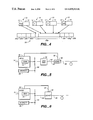
- FIG. 4 is a diagram illustrating a stripping function performed by an ATM interface block within the device shown in FIG. 3 .
- FIGS. 5 and 6 are diagrams illustrating the device shown in FIG. 3 coupled to a host processor for implementing a variety of selectable transmission modes.
- the Synchronous Optical NETwork (SONET) physical layer device of the present invention is a single-chip device that enables data to be transmitted over a SONET communications link in a variety of standard and non-standard transmission modes. These transmission modes include transmitting ATM cells in SONET SPEs, transmitting PPP frames in ATM cells in SONET SPEs, transmitting PPP frames from a Universal Test and Operations Interface for ATM (UTOPIA) in SONET SPEs, and transmitting PPP frames directly in SONET SPEs.
- SONET SPEs transmitting ATM cells in SONET SPEs
- PPP frames in ATM cells in SONET SPEs
- UUTOPIA Universal Test and Operations Interface for ATM
- FIG. 1 is a diagram illustrating a standard ATM UNI cell 10 , which is formed of 53 octets, including a 5-octet header field 12 and a 48-octet payload field 14 .
- the header field includes a 4-bit GFC field, an 8 bit VPI field, a 16-bit VCI field, a 3-bit PT field, a 1-bit CLP field, and an 8-bit HEC field.
- the GFC Generic Flow Control
- the VPI Virtual Path Identifier
- a path includes several connections.
- An ATM “wire” may be viewed as a cable consisting of multiple bundles of wire, where each bundle has many individual pairs of communication wires. The path is analogous to the bundle of wires. Physically reconnecting a bundle at the end of the cable changes where all the connections in that bundle go. Similarly, if the ATM cells in an ATM connection are redirected based on the VPI, then all connections within that VPI are redirected.
- the VCI Virtual Channel Identifier
- the VCI defines the channel number that the ATM cell belongs to. The channel is a single unidirectional circuit between two points. For example, a first channel would be used to send data from point A to point B, while a second channel would be used to send data from point B to point A.
- the PT Payment Type
- the CLP Cell Loss Priority
- the HEC Header Error Control
- the payload field is the 48 octet ATM cell payload area.
- FIG. 2 is a diagram of a PPP frame 20 .
- PPP frame 20 includes a flag sequence field 20 a , an address field 20 b , a control field 20 c , a protocol field 20 d , a payload field 20 e , an padding field 20 f , an FCS field 20 g and a flag sequence field 20 h .
- the first Flag sequence field 20 a identifies the start of PPP frame 20 and is formed of a single octet, such as 0x7E.
- Address field 20 b is formed of a single octet, such as 0XFF.
- the link control protocol (LCP or management protocol) may drop this field since a PPP connection is always point-to-point and thus an address is not required.
- Control field 20 c is formed of a single octet, such as 0x03, which may also be dropped by the LCP in compressed mode.
- Protocol field 20 d is a 2-octet field identifying the content type of the payload.
- Payload field 20 e includes zero or more octets of data to be transported. The maximum length of payload field 20 e is normally 1500 octets, but larger payloads may be negotiated.
- Padding field 20 f allows the payload field to be padded by the sender.
- FCS field 20 g is a frame check sequence field used for implementing a cyclic redundancy check (CRC) over the address, control, protocol and payload fields 20 b - 20 e .
- FCS field 20 g is normally two octets. However, for purposes of transmitting PPP directly over SONET, a 4-octet FCS field is recommended. The specification for the FCS field is given in ISO 3309.
- the second Flag sequence field 20 h identifies the end of the PPP frame and consists of a single octet, 0x7E.
- an octet stuffing procedure is used.
- each of these octets are replaced with a two octet sequence, consisting of a control escape octet 0x7D followed by the result of exclusive-ORing the octet with the value 0x20.
- a control escape octet 0x7D followed by the result of exclusive-ORing the octet with the value 0x20.
- the octet 0x7E is replaced the octets 0x7D and 0x9E.
- This is called octet stuffing since an additional octet was “stuffed” into the data stream to prevent misinterpretation.
- the octets 0x7D and 0x9E will be received by the far end of the system and will not be interpreted as a flag sequence but instead, the octet 0x7D will be discarded, and the octet 0x9E will be exclusive-OR'ed with 0x20 to recover the original octet 0x7E.
- Control values that are replaced during octet stuffing include the flag sequence, the control escape and other values that are negotiated when setting up the PPP link.
- PPP processing refers to receiving a protocol data unit, inserting the flag sequence, calculating, checking and inserting the FCS and providing octet stuffing.
- the remaining fields in the PPP frame are processed typically by firmware.
- FIG. 3 is a block diagram of a single-chip SONET physical layer device 30 which is capable of transmitting ATM cells and PPP frames in SONET SPEs in a variety of transmission modes according to the present invention.
- SONET device 30 includes control port 32 , UTOPIA bus interface port 34 , a standard bus interface port 36 , and a SONET interface port 38 .
- SONET device 30 further includes control and management interface block 40 , enhanced UTOPIA interface block 42 , PPP processing block 44 , SONET framer block 46 and SONET line interface 48 .
- Control and management interface block 40 is coupled between control port 32 and blocks 42 , 44 , 46 and 48 .
- Control and management interface block 40 includes a plurality of status registers, programmable control registers and related control logic for initializing the device to operate in one of the selected transmission modes and for otherwise controlling and managing the various blocks within device 30 .
- Enhanced UTOPIA interface block 42 is coupled between UTOPIA bus interface port 34 , PPP processing block 44 and SONET framer block 46 .
- PPP processing block is coupled between standard bus interface port 36 , enhanced UTOPIA interface block 42 and SONET framer block 46 .
- SONET framer block 46 is coupled to SONET line interface 48 , which is coupled to SONET interface port 38 .
- ATM cells are sequentially received from an ATM Segmentation And Reassembly (SAR) processor or cell processor (not shown), for example, through UTOPIA bus interface port 34 .
- Enhanced UTOPIA interface block 42 collects the received ATM cells in an array of storage elements, such as a stack of FIFOs. Once collected, the ATM cells are filtered and buffered in a known manner. The resulting cells are then passed to SONET framer block 46 .
- enhanced UTOPIA interface block 42 is constructed to conform with the UTOPIA Level 2 standard specified in ATM Forum Document af-phy-0039.00. In another embodiment, enhanced UTOPIA interface block 42 is constructed to conform with the UTOPIA Level 1 standard.
- Enhanced UTOPIA interface block 42 also includes additional processing circuitry for operating in non-standard transmission modes, as described in greater detail below.
- SONET framer block 46 receives the ATM cells from Enhanced UTOPIA interface block 42 and places the cells in the SPE of a SONET frame.
- SONET framer block 46 is constructed consistent with standards CCITT (ITU) 6.708, 6.709, 6.783 and I.432.
- the SONET frame is then passed to line interface 48 for transmission through SONET interface port 38 .
- Line interface 48 is responsible for clock generation and recovery during transmit and receive operations.
- line interface 48 is constructed consistent with the following standards, ANSI T1.E1.2/92-020R2, T1.M1.3/93-005R1 and ATM Forum atm93-1049r1.4.
- line interface 48 is constructed consistent with the “SONET/SDH Interface CMOS Core (SSI)” available from LSI Logic Corporation.
- SSI SONET/SDH Interface CMOS Core
- SONET framer block 46 When a SONET frame is received at SONET interface port 38 , the reverse path is followed.
- the received SONET frame is passed through line interface 48 to SONET framer block 46 , which extracts the ATM cells from the SONET SPE and passes the extracted ATM cells to Enhanced UTOPIA interface block 42 .
- Enhanced UTOPIA interface block 42 then transmits the ATM cells to the ATM SAR or cell processor (not shown) through UTOPIA bus interface port 34 .
- SONET device 30 is also capable of transmitting PPP frames in ATM cells in SONET SPEs.
- a remote ATM Adaption Layer (not shown) receives a PPP frame, segments the PPP frame into the payload fields of a plurality of ATM cells, and generates the cell headers.
- the ATM cells are then transmitted sequentially over a UTOPIA bus to UTOPIA bus interface port 34 .
- Enhanced UTOPIA interface block 42 receives the ATM cells and passes the cells to SONET framer block 46 for placement into a SONET SPE and transmission through SONET line interface 48 and SONET interface port 38 , as described above.
- the reverse path is also the same as that described above.
- device 30 is configured to transmit PPP from a UTOPIA interface within SONET SPEs.
- This transmission mode allows a standard ATM host processor which has no built-in or external PPP/HDLC capability to communicate with a SONET physical interface over a UTOPIA interface bus, and transmit PPP frames over the SONET communication link.
- the ATM Adaption Layer associated with the host processor segments a protocol data unit to be transmitted into the ATM cell payload fields, forms the ATM cell header fields, and passes the resulting ATM cells to device 30 through UTOPIA bus interface port 34 .
- Enhanced UTOPIA interface block 42 retrieves the protocol data unit from the ATM cell payload fields by stripping away the ATM header fields and optionally saving the ATM header field of one of the ATM cells. The protocol data unit and the optional remaining header field are then passed to PPP processing block 44 . In one embodiment, the Enhanced UTOPIA interface block 42 saves the header field of the first ATM cell of the protocol data unit.
- FIG. 4 is a diagram illustrating the stripping function performed by UTOPIA interface block 42 .
- the protocol data unit is carried by a set of ATM cells 10 , which are sequentially received by block 42 .
- Each of the ATM cells 10 includes a cell header field 12 and a cell payload field 14 .
- Block 42 has control circuitry for identifying the first and last ATM cells of the protocol data unit.
- Block 42 optionally stores the header field 12 of the first ATM cell 10 and discards the header fields 12 of all subsequent ATM cells 10 .
- the first header field 12 and the extracted protocol data unit are then passed to PPP processing block 44 .
- PPP processing block 44 temporarily stores the data frame within an array of memory storage elements, such as a FIFO, and forms a PPP frame 20 by placing the first header field 12 and the extracted protocol data unit in payload field 20 e .
- PPP processing block 44 also inserts the flag sequence in frames 20 a and 20 h , calculates, checks and inserts the FCS in field 20 g and provides octet stuffing as described above.
- the first header field 12 is preferably placed at the front of PPP payload field 20 e . This facilitates subsequent recovery of the cell header fields of the remaining ATM cells.
- PPP processing block 44 uses a fixed protocol field 20 d , the address and control fields 20 b and 20 c can be negotiated away.
- the resulting PPP frame 20 is then passed to SONET framer block 46 and loaded by row into a SONET SPE, creating a large bandwidth gain. Multiple PPP frames can be loaded into a single SONET SPE, and a single PPP frame can be divided between two consecutive SONET SPEs.
- SONET framer block 46 provides the SONET frames to line interface block 48 for transmission through SONET interface port 38 , as described above.
- UTOPIA interface block 42 strips the cell header fields from all of the ATM cells.
- SONET framer block 46 receives a SONET frame from line interface block 48 , extracts the PPP frame from the SPE of the SONET, frame and passes the PPP frame to PPP processing block 44 .
- PPP processing block 44 extracts the ATM cell header field from the beginning of the PPP payload field, extracts the protocol data unit from the remainder of the PPP payload field data and provides the ATM cell header and the protocol data unit to enhanced UTOPIA interface block 42 .
- Block 42 segments the protocol data unit into 48 octet sized pieces that fit into the ATM cell payload fields 14 .
- UTOPIA interface block 42 then generates the header fields 12 for each of the ATM cells 10 based on the header field extracted from the PPP payload field. Block 42 then transmits the ATM cells 30 through UTOPIA bus interface port 34 .
- UTOPIA interface block 42 is constructed consistent with the UTOPIA standards listed above, it has additional circuitry to enable the block to detect the first ATM cell of a protocol data unit, strip out the payload field of each ATM cell, store one of the cell header fields, and detect the last ATM cell of the protocol data unit in order to inform PPP processing block 44 to end the PPP frame.
- PPP processing block 4 is constructed consistent with IETF RFC 3548, RFC 1549 and ISO 3309.
- Increased performance is possible by enhancing framer block 46 to be able to strip out padding, length and CRC bytes from the ATM AAL 5 PDU trailer, prior to PPP processing. By stripping out these bytes, less “overhead” bytes need to be transmitted, thus improving bandwidth efficiency. This effective gain would be a programmable mode specific to AAL 5 traffic. This also requires that the receiving end be able to recreate these components. Although this transmission mode is not standard, it inter-operates easily with existing host devices, and provides dramatic improvement in bandwidth utilization.
- the third transmission mode allows a host processor without PPP/HDLC capability to transmit and receive protocol data units in PPP frames within SONET SPEs through device 30 .
- the host processor transmits the address, control and payload fields, including the start and end of frame indications, for a PPP frame over a standard bus to standard bus interface port 36 .
- the host processor receives the same fields in return when receiving a protocol data unit from device 30 .
- the address and control fields for the PPP frame are negotiated away.
- PPP processing block 44 of device 30 receives the protocol data unit and the associated fields from standard bus interface port 36 , forms a PPP frame as discussed above, and passes the PPP frame to SONET framer block 46 .
- SONET framer block 46 loads the PPP frame into a SONET SPE and passes the SONET frame to line interface block 48 for transmission through SONET interface port 38 .
- SONET framer block 46 is of a type capable of handling streams of data such that a PPP payload can be loaded by row into the SONET SPE.
- FIGS. 5 and 6 are diagrams illustrating the SONET physical layer device of the present invention coupled to a host processor for implementing the transmission modes discussed above.
- host processor 50 is coupled to UTOPIA interface port 34 through an ATM SAR device 52 .
- Host processor 50 has a port 54 for transmitting and receiving data units according to a selected protocol. For example, port 54 may be coupled to an Ethernet communications link.
- Host processor 50 has a DMA controller 56 which stores the protocol data units in memory 58 , over bus 60 .
- Host processor 50 also has a control output which is coupled to control port 32 of device 30 .
- Host processor 50 uses the control output for configuring device 30 to operate in one of the selectable transmission modes. For example, with the circuit shown in FIG.
- device 30 can be programmed to operate in one of the first two transmission modes discussed above, including transmitting ATM cells in SONET SPEs or PPP frames in ATM cells in SONET SPEs, and transmitting PPP frames from a UTOPIA interface in SONET SPEs.
- DMA controller 56 retrieves protocol data unit to be transmitted from memory 58 and provides data unit to, ATM SAR circuit 52 .
- ATM SAR circuit 52 segments the data unit into 48 octet-sized pieces that fit into the ATM cell payload fields and generates a header field for each ATM cell.
- ATM SAR circuit 60 then transmits the ATM cells to UTOPIA bus interface port 34 over UTOPIA bus 62 .
- bus 60 is coupled directly to standard bus interface port 36 of device 30 .
- the same reference numerals are used in FIG. 6 as were used in FIG. 5 for the same or similar elements.
- the control output of host processor 50 is coupled to control port 32 of device 30 , and host processor 50 configures device 30 to transmit PPP frames directly in SONET SPEs.
- Host processor 50 transmits the address, control and payload fields for a PPP frame over bus 60 through DMA controller 56 and memory 58 .
- Host processor 50 receives the same fields in return when receiving a data unit from device 30 .
- PPP processing block 44 in device 30 receives the data unit and its associated fields through standard bus interface port 36 , forms a PPP frame and passes the PPP frame to SONET framer block 46 for transmission in a SONET SPE as discussed above.
- the SONET physical device of the present invention is constructed on a single integrated circuit, which reduces the board space required to implement the circuit and the resulting cost of its manufacture.
- the device inter-operates with multiple standard and non-standard data encapsulation mechanisms, and allows packet transmission using the PPP protocol over a SONET communication link for maximum bandwidth utilization.
- SONET communication links are expensive and crowded with data traffic.
- the SONET physical layer device of the present invention allows data traffic to be transported readily in local or campus networks according to RFC 1619 with a large performance gain for little or no increased cost.
- PDUs protocol data units
- 64 octets is the size of acknowledgement packets used in Ethernet and other protocols.
- 1500 octets is the maximum size protocol data unit for non-enhanced Ethernet.
- 384 octets is the size theorized to be a result of legacy data traffic from protocols with a maximum 384 octet data bit size. This size information was used to calculate efficiency of data transport with the various transmission modes of the present invention.
- the transport efficiency of a 48-octet payload in a 53-octet ATM cell is 90.57w. This is the number typically quoted for ATM transport systems.
- the decrease in efficiency shown in Table 1 comes from the necessity of adding more protocol layers (the AAL 5 layer) to support the various size PDUs and to provide error checking across the PDU. Additional overhead is incurred from mapping the ATM cells into the SONET frame.
- Transporting PPP frames in ATM cells over SONET consists of adding the PPP flag sequences, control fields, etc., to the PDU as well as performing byte stuffing.
- the PPP processed PDU is then segmented into standard ATM cells for transport.
- control overhead could be negotiated down to 7 octets, and that byte stuffing would only be required for 2 octet values uniformly across the PDU (or one out of 128 octets would require stuffing).
- Table 2 shows the transport efficiency for this mode of operation. In this mode of operation, a layer of PPP processing has been added but there has been no gain in transport efficiency.
- Transporting PPP frames from a UTOPIA interface over SONET results in a significant increase in efficiency, as shown in Table 3.
- the increase in efficiency is gained by stripping the ATM cell headers from the PDU.
- Transporting PPP direct over SONET results in essentially the same transport efficiencies as those shown in Table 3.
- the 4 bytes added to recover the ATM cell header in the previous mode of operation would be replaced by another addressing mechanism, but the efficiencies would remain substantially the same.
- the primary distinction between these two modes of operation is that the ATM segmentation and reassembly function is totally removed, and the data no longer has to pass through the UTOPIA bus interface.
- the SONET physical layer device of the present invention can be constructed to operate at different transmission rates, such as STS-1, STS-3C and STS-12, using the same principals.
- the device can be configured with its surrounding components to operate in one of the selectable transmission modes during board level design or can be programmed during operation.
- the device can be constructed as a core or a macro within a larger integrated circuit design specification.
- the device can be constructed with multiplexed bus lines in order to achieve a smaller number of pins on the integrated circuit package.
- the device is constructed without a line interface block.
- an external line driver is used, which allows the use of varying types of line drivers.
- multiple instances, such as four or eight, of the device can be place on a single integrated circuit to provide multiple transmission channels for a line card router, for example.
Abstract
Description
| TABLE 1 | ||||
| # of ATM | ||||
| Cells | Octet | SONET | ||
| required | Total | Efficiency | Efficiency | |
| Size | for | Octets in | of Cells | (783* |
| of PDU | Transport | ATM Cells | (Oe) | Oe)/810 |
| 64 | 2 | 106 | 60.37% | 58.36% |
| 384 | 9 | 477 | 64.81% | 62.65% |
| 1500 | 32 | 1696 | 88.44% | 85.49% |
| *Extra ATM Cell required for additional AAL5 overhead bytes | ||||
| TABLE 2 | |||||
| # of ATM | |||||
| Size of | Cells | Octet | |||
| Size | PPP | Required | Total | Efficiency | SONET |
| of | Processed | for | Octets in | of Cells | Efficiency |
| PDU | PDU | Transport | ATM Cells | (Oe) | (783*Oe)/810 |
| 64 | 72 | 2 | 106 | 60.37% | 58.36% |
| 384 | 394 | 9 | 477 | 64.81% | 62.65% |
| 1500 | 1519 | 32 | 1696 | 88.44% | 85.49% |
| TABLE 3 | |||
| Size of PPP | |||
| Processed PDU | |||
| (4 bytes added for | |||
| Size of | first ATM cell | Octet Efficiency | SONET Efficiency |
| PDU | header) | of Cells (Oe) | (783*Oe)/810 |
| 64 | 76 | 84.21% | 81.40% |
| 384 | 398 | 96.48% | 93.26% |
| 1500 | 1523 | 98.49% | 95.21% |
Claims (12)
Priority Applications (1)
| Application Number | Priority Date | Filing Date | Title |
|---|---|---|---|
| US09/464,267 US6839352B1 (en) | 1997-06-02 | 1999-12-17 | SONET physical layer device having ATM and PPP interfaces |
Applications Claiming Priority (2)
| Application Number | Priority Date | Filing Date | Title |
|---|---|---|---|
| US08/867,249 US6075788A (en) | 1997-06-02 | 1997-06-02 | Sonet physical layer device having ATM and PPP interfaces |
| US09/464,267 US6839352B1 (en) | 1997-06-02 | 1999-12-17 | SONET physical layer device having ATM and PPP interfaces |
Related Parent Applications (1)
| Application Number | Title | Priority Date | Filing Date |
|---|---|---|---|
| US08/867,249 Continuation US6075788A (en) | 1997-06-02 | 1997-06-02 | Sonet physical layer device having ATM and PPP interfaces |
Publications (1)
| Publication Number | Publication Date |
|---|---|
| US6839352B1 true US6839352B1 (en) | 2005-01-04 |
Family
ID=25349420
Family Applications (2)
| Application Number | Title | Priority Date | Filing Date |
|---|---|---|---|
| US08/867,249 Expired - Lifetime US6075788A (en) | 1997-06-02 | 1997-06-02 | Sonet physical layer device having ATM and PPP interfaces |
| US09/464,267 Expired - Fee Related US6839352B1 (en) | 1997-06-02 | 1999-12-17 | SONET physical layer device having ATM and PPP interfaces |
Family Applications Before (1)
| Application Number | Title | Priority Date | Filing Date |
|---|---|---|---|
| US08/867,249 Expired - Lifetime US6075788A (en) | 1997-06-02 | 1997-06-02 | Sonet physical layer device having ATM and PPP interfaces |
Country Status (2)
| Country | Link |
|---|---|
| US (2) | US6075788A (en) |
| EP (1) | EP0883323A3 (en) |
Cited By (11)
| Publication number | Priority date | Publication date | Assignee | Title |
|---|---|---|---|---|
| US20030007513A1 (en) * | 2001-06-13 | 2003-01-09 | International Business Machines Corporation | STM-1 to STM-64 SDH/SONET framer with data multiplexing from a series of configurable I/O ports |
| US20030112758A1 (en) * | 2001-12-03 | 2003-06-19 | Pang Jon Laurent | Methods and systems for managing variable delays in packet transmission |
| US20040151177A1 (en) * | 2000-06-26 | 2004-08-05 | Burton Tom E. | Device to receive, buffer, and transmit packets of data in a packet switching network |
| US20040228355A1 (en) * | 2000-03-30 | 2004-11-18 | Azanda Network Devices, Inc. | Methods and apparatus for dynamically allocating bandwidth between ATM cells and packets |
| US20050238028A1 (en) * | 2001-07-30 | 2005-10-27 | Keller Richard B | Programmable sonet framing |
| US20060282489A1 (en) * | 2000-09-08 | 2006-12-14 | Khan Shoab A | Hardware function generator support in a DSP |
| US20060287742A1 (en) * | 2001-12-03 | 2006-12-21 | Khan Shoab A | Distributed processing architecture with scalable processing layers |
| US20070047554A1 (en) * | 2001-05-18 | 2007-03-01 | Denton I Claude | Multi-stage SONET overhead processing |
| US20070081466A1 (en) * | 2000-03-17 | 2007-04-12 | Keiichiro Tsukamoto | ATM cell service apparatus accommodating an ATM cell in an optical asynchronous communications network through a North America asynchronous communications network |
| US20080126812A1 (en) * | 2005-01-10 | 2008-05-29 | Sherjil Ahmed | Integrated Architecture for the Unified Processing of Visual Media |
| CN100440757C (en) * | 2006-03-21 | 2008-12-03 | 华为技术有限公司 | Optical repeater, message handling system in point-to-point protocol and processing method |
Families Citing this family (60)
| Publication number | Priority date | Publication date | Assignee | Title |
|---|---|---|---|---|
| US6791947B2 (en) | 1996-12-16 | 2004-09-14 | Juniper Networks | In-line packet processing |
| US6075788A (en) * | 1997-06-02 | 2000-06-13 | Lsi Logic Corporation | Sonet physical layer device having ATM and PPP interfaces |
| KR100222180B1 (en) * | 1997-06-28 | 1999-10-01 | 김영환 | Apparatus of processing the aal by cpu at atm terminal and a method thereof |
| GB2329550A (en) * | 1997-09-22 | 1999-03-24 | Northern Telecom Ltd | Transporting multi-protocol datagrams over an asynchronous virtual channel |
| US6202094B1 (en) * | 1997-11-07 | 2001-03-13 | International Business Machines Corporation | Adding links simultaneously to a multilink bundle using bandwidth allocation protocol |
| JP3204304B2 (en) * | 1997-12-12 | 2001-09-04 | 日本電気株式会社 | ATM cell transmission system |
| KR100267532B1 (en) * | 1997-12-30 | 2000-10-16 | 서평원 | Module for atm interface in atm communication terminal |
| US6731876B1 (en) * | 1998-02-23 | 2004-05-04 | Nippon Telegraph And Telephone Corporation | Packet transmission device and packet transmission system |
| AU771091B2 (en) * | 1998-06-19 | 2004-03-11 | Juniper Networks, Inc. | Device for performing IP forwarding and ATM switching |
| US6980543B1 (en) * | 1998-06-19 | 2005-12-27 | Juniper Networks, Inc. | Interconnect network for operation within a communication node |
| EP1748617A3 (en) * | 1998-09-11 | 2011-02-09 | Hitachi, Ltd. | IP packet communication apparatus |
| US6765911B1 (en) * | 1999-02-03 | 2004-07-20 | International Business Machines Corporation | Communications adapter for implementing communications in a network and providing multiple modes of communications |
| US20020175276A1 (en) * | 2001-02-06 | 2002-11-28 | Smith Alan Dane | Method and apparatus for determining a position of a movable barrier |
| EP1155594A1 (en) * | 1999-02-23 | 2001-11-21 | Siemens Aktiengesellschaft | Time-critical control of data to a sequentially controlled interface with asynchronous data transmission |
| CA2265346A1 (en) * | 1999-03-17 | 2000-09-17 | Pmc-Sierra Ltd. | Pos-phy interface for interconnection of physical layer devices and link layer devices |
| US6594279B1 (en) * | 1999-04-22 | 2003-07-15 | Nortel Networks Limited | Method and apparatus for transporting IP datagrams over synchronous optical networks at guaranteed quality of service |
| EP1180273B1 (en) * | 1999-06-02 | 2005-07-20 | Siemens Aktiengesellschaft | System and method for transmitting data |
| US6671271B1 (en) | 1999-06-03 | 2003-12-30 | Fujitsu Network Communications, Inc. | Sonet synchronous payload envelope pointer control system |
| US7068661B1 (en) | 1999-07-13 | 2006-06-27 | Alcatel Canada Inc. | Method and apparatus for providing control information in a system using distributed communication routing |
| US6990103B1 (en) * | 1999-07-13 | 2006-01-24 | Alcatel Canada Inc. | Method and apparatus for providing distributed communication routing |
| US6963572B1 (en) * | 1999-10-22 | 2005-11-08 | Alcatel Canada Inc. | Method and apparatus for segmentation and reassembly of data packets in a communication switch |
| US6892172B1 (en) * | 2000-02-16 | 2005-05-10 | Raj Kumar Singh | Customizable simulation model of an ATM/SONET framer for system level verification and performance characterization |
| US6778561B1 (en) * | 2000-02-23 | 2004-08-17 | Cypress Semiconductor Corp. | Hybrid data transport scheme over optical networks |
| US6771663B1 (en) * | 2000-02-23 | 2004-08-03 | Cypress Semiconductor Corp. | Hybrid data transport scheme over optical networks |
| US6973084B1 (en) * | 2000-02-23 | 2005-12-06 | Cypress Semiconductor Corp. | Hybrid data transport scheme over optical networks |
| US6999479B1 (en) * | 2000-02-23 | 2006-02-14 | Cypress Semiconductor Corp. | Hybrid data transport scheme over optical networks |
| US7006525B1 (en) * | 2000-02-23 | 2006-02-28 | Cypress Semiconductor Corp. | Hybrid data transport scheme over optical networks |
| US6847644B1 (en) * | 2000-02-23 | 2005-01-25 | Cypress Semiconductor Corp. | Hybrid data transport scheme over optical networks |
| EP1134923A1 (en) * | 2000-03-17 | 2001-09-19 | Alcatel | Method and multiplexer for transmitting asynchronous data packets over a synchronous digital data transmission network |
| US6965603B1 (en) | 2000-03-20 | 2005-11-15 | Cortina Systems, Inc. | Circuits for combining ATM and packet data on an optical fiber |
| US6810039B1 (en) | 2000-03-30 | 2004-10-26 | Azanda Network Devices, Inc. | Processor-based architecture for facilitating integrated data transfer between both atm and packet traffic with a packet bus or packet link, including bidirectional atm-to-packet functionally for atm traffic |
| US6751224B1 (en) | 2000-03-30 | 2004-06-15 | Azanda Network Devices, Inc. | Integrated ATM/packet segmentation-and-reassembly engine for handling both packet and ATM input data and for outputting both ATM and packet data |
| FI20001312A (en) * | 2000-05-31 | 2001-12-01 | Nokia Networks Oy | Formation of a telecommunications network |
| US6385209B1 (en) * | 2000-06-14 | 2002-05-07 | Pluris, Inc. | Method and apparatus for mapping data packets between lines of differing capacity at a router interface |
| US6831932B1 (en) * | 2000-07-14 | 2004-12-14 | Level 3 Communications, Inc. | Transfer of SONET traffic over a packet-switched network |
| US20030152182A1 (en) * | 2000-08-22 | 2003-08-14 | Pai B. Anand | Optical exchange method, apparatus and system for facilitating data transport between WAN, SAN and LAN and for enabling enterprise computing into networks |
| US6765916B1 (en) | 2000-12-30 | 2004-07-20 | Redback Networks Inc. | Method and apparatus for processing of multiple protocols within data transmission signals |
| US7486686B2 (en) * | 2001-02-26 | 2009-02-03 | Vitesse Semiconductor Corporation | Method and apparatus for scheduling data on a medium |
| JP4686875B2 (en) * | 2001-03-01 | 2011-05-25 | パナソニック株式会社 | Data communication device |
| US6959008B2 (en) * | 2001-03-31 | 2005-10-25 | Redback Networks Inc. | Alignment of TDM-based signals for packet transmission using framed and unframed operations |
| US7593432B2 (en) * | 2001-03-31 | 2009-09-22 | Redback Networks Inc. | Method and apparatus for deframing signals |
| US6950446B2 (en) | 2001-03-31 | 2005-09-27 | Redback Networks Inc. | Method and apparatus for simultaneously sync hunting signals |
| US6941381B2 (en) * | 2001-03-31 | 2005-09-06 | Redback Networks Inc. | Method and apparatus for sync hunting signals |
| ITMI20010726A1 (en) * | 2001-04-05 | 2002-10-05 | Cit Alcatel | METHOD AND APPARATUS TO MAP FAST ETHERNET DATA INTERFACES IN A SINGLE VC-4 VIRTUAL CONTAINER OF A STM-1 / OC-3 PAYLOAD TRANSMITTED IN U |
| GB0110437D0 (en) * | 2001-04-27 | 2001-06-20 | Marconi Comm Ltd | A transmission method |
| US7002967B2 (en) | 2001-05-18 | 2006-02-21 | Denton I Claude | Multi-protocol networking processor with data traffic support spanning local, regional and wide area networks |
| US6567413B1 (en) * | 2001-05-18 | 2003-05-20 | Network Elements, Inc. | Optical networking module including protocol processing and unified software control |
| US20020194363A1 (en) * | 2001-06-14 | 2002-12-19 | Cypress Semiconductor Corp. | Programmable protocol processing engine for network packet devices |
| US20020191621A1 (en) * | 2001-06-14 | 2002-12-19 | Cypress Semiconductor Corp. | Programmable protocol processing engine for network packet devices |
| US7349401B2 (en) * | 2001-09-05 | 2008-03-25 | Symmetricom, Inc. | Bonded G.shdsl links for ATM backhaul applications |
| US7324539B1 (en) | 2001-11-28 | 2008-01-29 | Redback Networks Inc. | Method and apparatus for processing channelized and unchannelized data within a signal |
| US7075951B1 (en) | 2001-11-29 | 2006-07-11 | Redback Networks Inc. | Method and apparatus for the operation of a storage unit in a network element |
| US7130948B2 (en) * | 2002-08-02 | 2006-10-31 | Bian Qiyong B | Flexible interrupt handling methods for optical networking apparatuses with multiple multi-protocol optical networking modules |
| US7324524B2 (en) * | 2002-10-29 | 2008-01-29 | Mindspeed Technologies, Inc. | Pseudo synchronous machine |
| KR100475879B1 (en) * | 2002-11-11 | 2005-03-11 | 한국전자통신연구원 | An internet phone terminal for wire and wireless communication |
| US7257131B2 (en) * | 2002-12-13 | 2007-08-14 | Cisco Technology, Inc. | System and method for communicating traffic between a cell site and a central office in a telecommunications network |
| CN100440824C (en) * | 2003-01-28 | 2008-12-03 | 华为技术有限公司 | System and method for switchingin and transmission of different data frames in digital transmission network |
| KR100526544B1 (en) * | 2003-06-02 | 2005-11-03 | 삼성전자주식회사 | Optical transmission network and method for providing broadcasting services |
| US6956847B2 (en) * | 2003-06-19 | 2005-10-18 | Cisco Technology, Inc. | Multi-rate, multi-protocol, multi-port line interface for a multiservice switching platform |
| KR100557138B1 (en) * | 2003-07-16 | 2006-03-03 | 삼성전자주식회사 | Video Data Transmitting Method In Optical Network |
Citations (13)
| Publication number | Priority date | Publication date | Assignee | Title |
|---|---|---|---|---|
| US5375121A (en) | 1991-08-28 | 1994-12-20 | Fujitsu Limited | ATM cell assembling and disassembling system and method |
| US5414707A (en) | 1993-12-01 | 1995-05-09 | Bell Communications Research, Inc. | Broadband ISDN processing method and system |
| US5600650A (en) | 1995-07-07 | 1997-02-04 | Sun Microsystems, Inc. | Method and apparatus for synthesizing clock signals for use with an asynchronous transfer mode system having selectable data transmission rates |
| US5625625A (en) * | 1995-07-07 | 1997-04-29 | Sun Microsystems, Inc. | Method and apparatus for partitioning data load and unload functions within an interface system for use with an asynchronous transfer mode system |
| US5717690A (en) | 1995-11-17 | 1998-02-10 | U.S. Robotics Corporation | Coordination and control of data streams that terminate at different termination units |
| US5742762A (en) * | 1995-05-19 | 1998-04-21 | Telogy Networks, Inc. | Network management gateway |
| US5748630A (en) * | 1996-05-09 | 1998-05-05 | Maker Communications, Inc. | Asynchronous transfer mode cell processing system with load multiple instruction and memory write-back |
| US5781320A (en) | 1996-08-23 | 1998-07-14 | Lucent Technologies Inc. | Fiber access architecture for use in telecommunications networks |
| US5835036A (en) | 1997-05-12 | 1998-11-10 | Cisco Systems Co. | Method of encoding data for transmission |
| US5835602A (en) | 1996-08-19 | 1998-11-10 | Pmc-Sierra Ltd. | Self-synchronous packet scrambler |
| US6041043A (en) * | 1996-10-25 | 2000-03-21 | Tektronix, Inc. | SONET path/ATM physical layer transmit/receive processor |
| US6075788A (en) * | 1997-06-02 | 2000-06-13 | Lsi Logic Corporation | Sonet physical layer device having ATM and PPP interfaces |
| US6343086B1 (en) * | 1996-09-09 | 2002-01-29 | Natural Microsystems Corporation | Global packet-switched computer network telephony server |
-
1997
- 1997-06-02 US US08/867,249 patent/US6075788A/en not_active Expired - Lifetime
-
1998
- 1998-05-28 EP EP98304238A patent/EP0883323A3/en not_active Withdrawn
-
1999
- 1999-12-17 US US09/464,267 patent/US6839352B1/en not_active Expired - Fee Related
Patent Citations (13)
| Publication number | Priority date | Publication date | Assignee | Title |
|---|---|---|---|---|
| US5375121A (en) | 1991-08-28 | 1994-12-20 | Fujitsu Limited | ATM cell assembling and disassembling system and method |
| US5414707A (en) | 1993-12-01 | 1995-05-09 | Bell Communications Research, Inc. | Broadband ISDN processing method and system |
| US5742762A (en) * | 1995-05-19 | 1998-04-21 | Telogy Networks, Inc. | Network management gateway |
| US5600650A (en) | 1995-07-07 | 1997-02-04 | Sun Microsystems, Inc. | Method and apparatus for synthesizing clock signals for use with an asynchronous transfer mode system having selectable data transmission rates |
| US5625625A (en) * | 1995-07-07 | 1997-04-29 | Sun Microsystems, Inc. | Method and apparatus for partitioning data load and unload functions within an interface system for use with an asynchronous transfer mode system |
| US5717690A (en) | 1995-11-17 | 1998-02-10 | U.S. Robotics Corporation | Coordination and control of data streams that terminate at different termination units |
| US5748630A (en) * | 1996-05-09 | 1998-05-05 | Maker Communications, Inc. | Asynchronous transfer mode cell processing system with load multiple instruction and memory write-back |
| US5835602A (en) | 1996-08-19 | 1998-11-10 | Pmc-Sierra Ltd. | Self-synchronous packet scrambler |
| US5781320A (en) | 1996-08-23 | 1998-07-14 | Lucent Technologies Inc. | Fiber access architecture for use in telecommunications networks |
| US6343086B1 (en) * | 1996-09-09 | 2002-01-29 | Natural Microsystems Corporation | Global packet-switched computer network telephony server |
| US6041043A (en) * | 1996-10-25 | 2000-03-21 | Tektronix, Inc. | SONET path/ATM physical layer transmit/receive processor |
| US5835036A (en) | 1997-05-12 | 1998-11-10 | Cisco Systems Co. | Method of encoding data for transmission |
| US6075788A (en) * | 1997-06-02 | 2000-06-13 | Lsi Logic Corporation | Sonet physical layer device having ATM and PPP interfaces |
Non-Patent Citations (3)
| Title |
|---|
| LSI LOGIC Promotion, "SONET/SDH Interface Core", (R20005 1995). |
| RFC 1549-Network Working Group W. Simpson, Editor Request for Comments: 1549 Daydreamer Category, PPP in HDLC Framing, (Dec. 1993), -http://andrew2.andrew.cmu.edu/rfc/rfc1549.html. |
| RFC 1619-Network Working Group W. Simpson Request for Comments: 1619 Daydreamer Category, "PPP over SONET/SDH" (May 1994), -http://andrew2.andrew.cmu.edu/rfc/rfc1619.html. |
Cited By (27)
| Publication number | Priority date | Publication date | Assignee | Title |
|---|---|---|---|---|
| US20070081466A1 (en) * | 2000-03-17 | 2007-04-12 | Keiichiro Tsukamoto | ATM cell service apparatus accommodating an ATM cell in an optical asynchronous communications network through a North America asynchronous communications network |
| US20040228355A1 (en) * | 2000-03-30 | 2004-11-18 | Azanda Network Devices, Inc. | Methods and apparatus for dynamically allocating bandwidth between ATM cells and packets |
| US7145910B2 (en) * | 2000-03-30 | 2006-12-05 | Cortina Systems, Inc. | Methods and apparatus for dynamically allocating bandwidth between ATM cells and packets |
| US20040151177A1 (en) * | 2000-06-26 | 2004-08-05 | Burton Tom E. | Device to receive, buffer, and transmit packets of data in a packet switching network |
| US20040208174A1 (en) * | 2000-06-26 | 2004-10-21 | Burton Tom E. | Device to receive, buffer, and transmit packets of data in a packet switching network |
| US7450583B2 (en) | 2000-06-26 | 2008-11-11 | Burton Tom E | Device to receive, buffer, and transmit packets of data in a packet switching network |
| US20110119520A1 (en) * | 2000-09-08 | 2011-05-19 | Avaz Networks | Hardware Function Generator Support in a DSP |
| US20060282489A1 (en) * | 2000-09-08 | 2006-12-14 | Khan Shoab A | Hardware function generator support in a DSP |
| US20070047554A1 (en) * | 2001-05-18 | 2007-03-01 | Denton I Claude | Multi-stage SONET overhead processing |
| US7746907B2 (en) | 2001-05-18 | 2010-06-29 | Denton I Claude | Multi-stage SONET overhead processing |
| US7161961B2 (en) * | 2001-06-13 | 2007-01-09 | International Business Machines Corporation | STM-1 to STM-64 SDH/SONET framer with data multiplexing from a series of configurable I/O ports |
| US20030007513A1 (en) * | 2001-06-13 | 2003-01-09 | International Business Machines Corporation | STM-1 to STM-64 SDH/SONET framer with data multiplexing from a series of configurable I/O ports |
| US20060285551A1 (en) * | 2001-06-13 | 2006-12-21 | Barker Kenneth J | Stm-1 to stm-64 sdh/sonet framer with data multiplexing from a series of configurable i/o ports |
| US8130792B2 (en) | 2001-06-13 | 2012-03-06 | International Business Machines Corporation | STM-1 to STM-64 SDH/SONET framer with data multiplexing from a series of configurable I/O ports |
| US20070008965A1 (en) * | 2001-07-30 | 2007-01-11 | Keller Richard B | Programmable SONET framing |
| US8374204B2 (en) * | 2001-07-30 | 2013-02-12 | Null Networks Llc | Programmable SONET framing |
| US20050238028A1 (en) * | 2001-07-30 | 2005-10-27 | Keller Richard B | Programmable sonet framing |
| US7894492B2 (en) | 2001-07-30 | 2011-02-22 | Keller Richard B | Programmable SONET framing |
| US7516320B2 (en) * | 2001-12-03 | 2009-04-07 | Quartics, Inc. | Distributed processing architecture with scalable processing layers |
| US20090328048A1 (en) * | 2001-12-03 | 2009-12-31 | Quartics, Inc. | Distributed Processing Architecture With Scalable Processing Layers |
| US20090316580A1 (en) * | 2001-12-03 | 2009-12-24 | Jon Laurent Pang | Methods and Systems for Managing Variable Delays in Packet Transmission |
| US7835280B2 (en) | 2001-12-03 | 2010-11-16 | Quartics, Inc. | Methods and systems for managing variable delays in packet transmission |
| US20060287742A1 (en) * | 2001-12-03 | 2006-12-21 | Khan Shoab A | Distributed processing architecture with scalable processing layers |
| US20030112758A1 (en) * | 2001-12-03 | 2003-06-19 | Pang Jon Laurent | Methods and systems for managing variable delays in packet transmission |
| US20110141889A1 (en) * | 2001-12-03 | 2011-06-16 | Jon Laurent Pang | Methods and Systems for Managing Variable Delays in Packet Transmission |
| US20080126812A1 (en) * | 2005-01-10 | 2008-05-29 | Sherjil Ahmed | Integrated Architecture for the Unified Processing of Visual Media |
| CN100440757C (en) * | 2006-03-21 | 2008-12-03 | 华为技术有限公司 | Optical repeater, message handling system in point-to-point protocol and processing method |
Also Published As
| Publication number | Publication date |
|---|---|
| EP0883323A3 (en) | 2000-02-23 |
| EP0883323A2 (en) | 1998-12-09 |
| US6075788A (en) | 2000-06-13 |
Similar Documents
| Publication | Publication Date | Title |
|---|---|---|
| US6839352B1 (en) | SONET physical layer device having ATM and PPP interfaces | |
| EP1005779B1 (en) | Device for performing ip forwarding and atm switching | |
| US6108336A (en) | AAL-5 SSCS for AAL-1 and AAL-2 in ATM networks | |
| US5987034A (en) | ATM cells within frame relay technology | |
| AU678045B2 (en) | Fast packet adaptation method for ensuring packet portability across diversified switching type networks | |
| JP4087559B2 (en) | Efficient transfer of Internet protocol packets using conformance layer 2 in asynchronous transmission mode | |
| US6456631B1 (en) | Communication control equipment and communication control method | |
| US5936967A (en) | Multi-channel broadband adaptation processing | |
| US5481544A (en) | Multi-channel broadband adaptation processing | |
| US6639916B1 (en) | AAL receiving circuit and method of processing ATM cells | |
| JPH07254904A (en) | Transfer system and switch device for variable length cell in atm | |
| US6032272A (en) | Method and apparatus for performing packet based policing | |
| JPH08214009A (en) | Pay load production of wide band cell | |
| US7944900B2 (en) | Base station modulator/demodulator and send/receive method | |
| JP3539551B2 (en) | Frame and transmission device for accommodating heterogeneous data traffic on common carrier | |
| EP1111827B1 (en) | STS-n with enhanced granularity | |
| US5991532A (en) | Method and apparatus for converting multimegabit-rate data into asynchronous transfer mode cells and vice versa | |
| JP3003648B2 (en) | LAN emulation method on ATM | |
| EP0949841A2 (en) | Low bandwidth AAL5 data communication system | |
| Xu et al. | A Unified Framing Protocol for Hybrid Data Transport | |
| GB2336270A (en) | AAL5 data communication | |
| EP1163822A1 (en) | Method and apparatus for performing packet based policing | |
| KR20050007746A (en) | Processing System And Method of Bridged Ethernet Encapsulation over ATM Adaptation Layer 5 of RFC 2684 for High Speed Ethernet to ATM Gateway |
Legal Events
| Date | Code | Title | Description |
|---|---|---|---|
| FEPP | Fee payment procedure |
Free format text: PAYOR NUMBER ASSIGNED (ORIGINAL EVENT CODE: ASPN); ENTITY STATUS OF PATENT OWNER: LARGE ENTITY |
|
| FPAY | Fee payment |
Year of fee payment: 4 |
|
| FPAY | Fee payment |
Year of fee payment: 8 |
|
| AS | Assignment |
Owner name: DEUTSCHE BANK AG NEW YORK BRANCH, AS COLLATERAL AG Free format text: PATENT SECURITY AGREEMENT;ASSIGNORS:LSI CORPORATION;AGERE SYSTEMS LLC;REEL/FRAME:032856/0031 Effective date: 20140506 |
|
| AS | Assignment |
Owner name: LSI CORPORATION, CALIFORNIA Free format text: CHANGE OF NAME;ASSIGNOR:LSI LOGIC CORPORATION;REEL/FRAME:033977/0397 Effective date: 20070404 |
|
| AS | Assignment |
Owner name: AGERE SYSTEMS LLC, PENNSYLVANIA Free format text: TERMINATION AND RELEASE OF SECURITY INTEREST IN PATENTS AT REEL/FRAME NO. 32856/0031;ASSIGNOR:DEUTSCHE BANK AG NEW YORK BRANCH;REEL/FRAME:034286/0872 Effective date: 20141118 Owner name: LSI CORPORATION, CALIFORNIA Free format text: TERMINATION AND RELEASE OF SECURITY INTEREST IN PATENTS AT REEL/FRAME NO. 32856/0031;ASSIGNOR:DEUTSCHE BANK AG NEW YORK BRANCH;REEL/FRAME:034286/0872 Effective date: 20141118 |
|
| FEPP | Fee payment procedure |
Free format text: PAYOR NUMBER ASSIGNED (ORIGINAL EVENT CODE: ASPN); ENTITY STATUS OF PATENT OWNER: LARGE ENTITY Free format text: PAYER NUMBER DE-ASSIGNED (ORIGINAL EVENT CODE: RMPN); ENTITY STATUS OF PATENT OWNER: LARGE ENTITY |
|
| AS | Assignment |
Owner name: INTEL CORPORATION, CALIFORNIA Free format text: ASSIGNMENT OF ASSIGNORS INTEREST;ASSIGNOR:LSI CORPORATION;REEL/FRAME:035090/0477 Effective date: 20141114 |
|
| AS | Assignment |
Owner name: AGERE SYSTEMS LLC, PENNSYLVANIA Free format text: TERMINATION AND RELEASE OF SECURITY INTEREST IN PATENT RIGHTS (RELEASES RF 032856-0031);ASSIGNOR:DEUTSCHE BANK AG NEW YORK BRANCH, AS COLLATERAL AGENT;REEL/FRAME:037684/0039 Effective date: 20160201 Owner name: LSI CORPORATION, CALIFORNIA Free format text: TERMINATION AND RELEASE OF SECURITY INTEREST IN PATENT RIGHTS (RELEASES RF 032856-0031);ASSIGNOR:DEUTSCHE BANK AG NEW YORK BRANCH, AS COLLATERAL AGENT;REEL/FRAME:037684/0039 Effective date: 20160201 |
|
| REMI | Maintenance fee reminder mailed | ||
| LAPS | Lapse for failure to pay maintenance fees | ||
| STCH | Information on status: patent discontinuation |
Free format text: PATENT EXPIRED DUE TO NONPAYMENT OF MAINTENANCE FEES UNDER 37 CFR 1.362 |
|
| FP | Lapsed due to failure to pay maintenance fee |
Effective date: 20170104 |