US6847014B1 - Method and apparatus for controlling the spatial temperature distribution across the surface of a workpiece support - Google Patents
Method and apparatus for controlling the spatial temperature distribution across the surface of a workpiece support Download PDFInfo
- Publication number
- US6847014B1 US6847014B1 US10/062,395 US6239502A US6847014B1 US 6847014 B1 US6847014 B1 US 6847014B1 US 6239502 A US6239502 A US 6239502A US 6847014 B1 US6847014 B1 US 6847014B1
- Authority
- US
- United States
- Prior art keywords
- temperature
- chuck
- heater
- workpiece
- layer
- Prior art date
- Legal status (The legal status is an assumption and is not a legal conclusion. Google has not performed a legal analysis and makes no representation as to the accuracy of the status listed.)
- Expired - Lifetime
Links
- 238000000034 method Methods 0.000 title claims description 27
- 238000010438 heat treatment Methods 0.000 claims abstract description 39
- 230000004907 flux Effects 0.000 claims description 20
- 239000000463 material Substances 0.000 claims description 7
- 230000008569 process Effects 0.000 claims description 7
- 239000002470 thermal conductor Substances 0.000 claims description 3
- 239000012774 insulation material Substances 0.000 claims 9
- 230000006698 induction Effects 0.000 claims 2
- 238000012544 monitoring process Methods 0.000 claims 2
- 239000012212 insulator Substances 0.000 abstract description 24
- 235000012431 wafers Nutrition 0.000 description 45
- 239000007789 gas Substances 0.000 description 12
- 238000010586 diagram Methods 0.000 description 11
- 239000002826 coolant Substances 0.000 description 10
- 238000001020 plasma etching Methods 0.000 description 7
- 238000001816 cooling Methods 0.000 description 6
- 238000005530 etching Methods 0.000 description 5
- 239000004065 semiconductor Substances 0.000 description 5
- 230000008901 benefit Effects 0.000 description 4
- 239000000919 ceramic Substances 0.000 description 4
- 239000012530 fluid Substances 0.000 description 4
- 239000010410 layer Substances 0.000 description 4
- 238000007789 sealing Methods 0.000 description 4
- 229910052734 helium Inorganic materials 0.000 description 3
- 239000001307 helium Substances 0.000 description 3
- SWQJXJOGLNCZEY-UHFFFAOYSA-N helium atom Chemical compound [He] SWQJXJOGLNCZEY-UHFFFAOYSA-N 0.000 description 3
- 150000002500 ions Chemical class 0.000 description 3
- 238000013459 approach Methods 0.000 description 2
- 238000009529 body temperature measurement Methods 0.000 description 2
- 238000006243 chemical reaction Methods 0.000 description 2
- 238000011161 development Methods 0.000 description 2
- 230000001939 inductive effect Effects 0.000 description 2
- 238000005259 measurement Methods 0.000 description 2
- 239000007769 metal material Substances 0.000 description 2
- 230000002093 peripheral effect Effects 0.000 description 2
- 229920000642 polymer Polymers 0.000 description 2
- 238000012545 processing Methods 0.000 description 2
- 239000000758 substrate Substances 0.000 description 2
- 230000003746 surface roughness Effects 0.000 description 2
- BNGXYYYYKUGPPF-UHFFFAOYSA-M (3-methylphenyl)methyl-triphenylphosphanium;chloride Chemical compound [Cl-].CC1=CC=CC(C[P+](C=2C=CC=CC=2)(C=2C=CC=CC=2)C=2C=CC=CC=2)=C1 BNGXYYYYKUGPPF-UHFFFAOYSA-M 0.000 description 1
- 239000012790 adhesive layer Substances 0.000 description 1
- XAGFODPZIPBFFR-UHFFFAOYSA-N aluminium Chemical compound [Al] XAGFODPZIPBFFR-UHFFFAOYSA-N 0.000 description 1
- 229910052782 aluminium Inorganic materials 0.000 description 1
- PNEYBMLMFCGWSK-UHFFFAOYSA-N aluminium oxide Inorganic materials [O-2].[O-2].[O-2].[Al+3].[Al+3] PNEYBMLMFCGWSK-UHFFFAOYSA-N 0.000 description 1
- 229910010293 ceramic material Inorganic materials 0.000 description 1
- 230000008859 change Effects 0.000 description 1
- 239000004020 conductor Substances 0.000 description 1
- 238000010276 construction Methods 0.000 description 1
- 230000008878 coupling Effects 0.000 description 1
- 238000010168 coupling process Methods 0.000 description 1
- 238000005859 coupling reaction Methods 0.000 description 1
- 230000009977 dual effect Effects 0.000 description 1
- 229920001971 elastomer Polymers 0.000 description 1
- 239000000806 elastomer Substances 0.000 description 1
- 230000005684 electric field Effects 0.000 description 1
- 229910052743 krypton Inorganic materials 0.000 description 1
- DNNSSWSSYDEUBZ-UHFFFAOYSA-N krypton atom Chemical compound [Kr] DNNSSWSSYDEUBZ-UHFFFAOYSA-N 0.000 description 1
- 238000003754 machining Methods 0.000 description 1
- 238000012986 modification Methods 0.000 description 1
- 230000004048 modification Effects 0.000 description 1
- 238000004886 process control Methods 0.000 description 1
- 230000000750 progressive effect Effects 0.000 description 1
- 239000010453 quartz Substances 0.000 description 1
- 238000000926 separation method Methods 0.000 description 1
- VYPSYNLAJGMNEJ-UHFFFAOYSA-N silicon dioxide Inorganic materials O=[Si]=O VYPSYNLAJGMNEJ-UHFFFAOYSA-N 0.000 description 1
- 239000002356 single layer Substances 0.000 description 1
- 238000012546 transfer Methods 0.000 description 1
Images


Classifications
-
- H—ELECTRICITY
- H01—ELECTRIC ELEMENTS
- H01L—SEMICONDUCTOR DEVICES NOT COVERED BY CLASS H10
- H01L21/00—Processes or apparatus adapted for the manufacture or treatment of semiconductor or solid state devices or of parts thereof
- H01L21/67—Apparatus specially adapted for handling semiconductor or electric solid state devices during manufacture or treatment thereof; Apparatus specially adapted for handling wafers during manufacture or treatment of semiconductor or electric solid state devices or components ; Apparatus not specifically provided for elsewhere
- H01L21/67005—Apparatus not specifically provided for elsewhere
- H01L21/67242—Apparatus for monitoring, sorting or marking
- H01L21/67248—Temperature monitoring
-
- H—ELECTRICITY
- H01—ELECTRIC ELEMENTS
- H01L—SEMICONDUCTOR DEVICES NOT COVERED BY CLASS H10
- H01L21/00—Processes or apparatus adapted for the manufacture or treatment of semiconductor or solid state devices or of parts thereof
- H01L21/02—Manufacture or treatment of semiconductor devices or of parts thereof
- H01L21/04—Manufacture or treatment of semiconductor devices or of parts thereof the devices having at least one potential-jump barrier or surface barrier, e.g. PN junction, depletion layer or carrier concentration layer
- H01L21/18—Manufacture or treatment of semiconductor devices or of parts thereof the devices having at least one potential-jump barrier or surface barrier, e.g. PN junction, depletion layer or carrier concentration layer the devices having semiconductor bodies comprising elements of Group IV of the Periodic System or AIIIBV compounds with or without impurities, e.g. doping materials
- H01L21/30—Treatment of semiconductor bodies using processes or apparatus not provided for in groups H01L21/20 - H01L21/26
- H01L21/302—Treatment of semiconductor bodies using processes or apparatus not provided for in groups H01L21/20 - H01L21/26 to change their surface-physical characteristics or shape, e.g. etching, polishing, cutting
- H01L21/306—Chemical or electrical treatment, e.g. electrolytic etching
- H01L21/3065—Plasma etching; Reactive-ion etching
-
- H—ELECTRICITY
- H01—ELECTRIC ELEMENTS
- H01L—SEMICONDUCTOR DEVICES NOT COVERED BY CLASS H10
- H01L21/00—Processes or apparatus adapted for the manufacture or treatment of semiconductor or solid state devices or of parts thereof
- H01L21/67—Apparatus specially adapted for handling semiconductor or electric solid state devices during manufacture or treatment thereof; Apparatus specially adapted for handling wafers during manufacture or treatment of semiconductor or electric solid state devices or components ; Apparatus not specifically provided for elsewhere
- H01L21/67005—Apparatus not specifically provided for elsewhere
- H01L21/67011—Apparatus for manufacture or treatment
- H01L21/67098—Apparatus for thermal treatment
- H01L21/67103—Apparatus for thermal treatment mainly by conduction
-
- H—ELECTRICITY
- H01—ELECTRIC ELEMENTS
- H01J—ELECTRIC DISCHARGE TUBES OR DISCHARGE LAMPS
- H01J2237/00—Discharge tubes exposing object to beam, e.g. for analysis treatment, etching, imaging
- H01J2237/20—Positioning, supporting, modifying or maintaining the physical state of objects being observed or treated
- H01J2237/2001—Maintaining constant desired temperature
Definitions
- a typical plasma etching apparatus comprises a reactor in which there is a chamber through which reactive gas or gases flow. Within the chamber, the gases are ionized into a plasma, typically by radio frequency energy. The highly reactive ions of the plasma gas are able to react with material, such as a polymer mask on a surface of a semiconductor wafer being processed into integrated circuits (IC's). Prior to etching, the wafer is placed in the chamber and held in proper position by a chuck or holder which exposes a top surface of the wafer to the plasma gas.
- chucks also sometimes called susceptors
- the chuck provides an isothermal surface and serves as a heat sink for the wafer.
- a semiconductor wafer is held in place for etching by mechanical clamping means.
- a semiconductor wafer is held in place by electrostatic force generated by an electric field between the chuck and wafer.
- the present invention is applicable to both types of chucks.
- the reactive ions of the plasma gas chemically react with portions of material on a face of the semiconductor wafer.
- Some processes cause some degree of heating of the wafer, but most of the heating is caused by the plasma.
- the chemical reaction between gas (ions and radicals) and wafer material is accelerated to some degree by the temperature rise of the wafer.
- Local wafer temperature and rate of chemical reaction at each microscopic point on the wafer are related to an extent that harmful unevenness in etching of material over a face of the wafer can easily result if the temperature of the wafer across its area varies too much.
- FIG. 1 illustrates one way to control wafer temperature during RIE.
- a coolant gas such as helium
- a coolant gas is admitted at a single pressure within a single thin space 102 between the bottom of the wafer 104 and the top of the chuck 106 which holds the wafer 104 .
- FIG. 2 illustrates a typical temperature distribution on the wafer 104 .
- the pressure loss at the peripheral portions of the wafer 104 causes the wafer 104 to be much hotter at the peripheral portions.
- the gas supply to each zone may have different composition or be set to a different pressure, thus varying the thermal conduction.
- Each zone's operating conditions may be set under recipe control, or even dynamically stabilized during each process step.
- Such schemes depend on redistributing the incoming heat flux from the plasma and extracting it into different regions. This is relatively effective at high power flux but will only give small temperature differentials at lower power flux. For instance, with about 1 W per cm 2 of uniform flux and about 3 mm sealing land, it is possible to get center to edge thermal gradients that lead to a 10° C. to 30° C. temperature increase near the wafer periphery. Thermal gradients of this magnitude can be very effective as a process control parameter.
- a primary purpose of the present invention is to solve these needs and provide further, related advantages.
- a chuck for a plasma processor comprises a temperature-controlled base, a thermal insulator, a flat support, and a heater.
- the temperature-controlled base has a temperature below the desired temperature of a workpiece.
- the thermal insulator is disposed over the temperature-controlled base.
- the flat support holds a workpiece and is disposed over the thermal insulator.
- a heater is embedded within the flat support and/or disposed on an underside of the flat support.
- the heater includes a plurality of heating elements that heat a plurality of corresponding heating zones. The power supplied and/or temperature of each heating element is controlled independently.
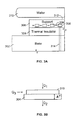
- FIG. 1 is a schematic elevational diagram of a support holding a wafer under process in accordance with the prior art
- FIG. 2 is a plot illustrating the temperature of a wafer and the pressure of a coolant in the apparatus of FIG. 1 in accordance with the prior art
- FIG. 3A is a schematic elevational diagram illustrating an apparatus for controlling the temperature of a workpiece in accordance with one embodiment of the present invention
- FIG. 3B illustrates a simplified schematic of thermal flow dynamic in the apparatus of FIG. 3A ;
- FIG. 4A is a schematic elevational diagram illustrating an apparatus with a combined single planar layer electrode and heater for controlling the temperature of a workpiece in accordance with another embodiment of the present invention
- FIG. 4B is a schematic top view illustrating an apparatus with a combined single planar layer electrode and heater for controlling the temperature of a workpiece in accordance with another embodiment of the present invention
- FIG. 5 is a schematic elevational diagram illustrating an apparatus for controlling the temperature of a workpiece using a lateral thermal break approach in accordance with another alternative embodiment of the present invention
- FIG. 6 is a flow diagram illustrating a method for controlling the temperature of a chuck in accordance with one embodiment of the present invention.
- FIG. 7 is a schematic diagram of a system for controlling the temperature of a chuck in accordance with one embodiment of the present invention.
- Embodiments of the present invention are described herein in the context of a method and apparatus for controlling the spatial temperature distribution across the surface of a workpiece support.
- Those of ordinary skill in the art will realize that the following detailed description of the present invention is illustrative only and is not intended to be in any way limiting. Other embodiments of the present invention will readily suggest themselves to such skilled persons having the benefit of this disclosure.
- FIG. 3A is a schematic elevational diagram illustrating an apparatus for controlling the temperature of a workpiece in accordance with one embodiment of the present invention.
- a base 302 or a heat exchanger supports a thermal insulator 304 .
- a support 306 preferably flat, is mounted over the thermal insulator 304 .
- a heater 308 is embedded in the support 306 .
- a workpiece 310 such as a wafer, is disposed over the support 306 .
- a thermal conductor 312 provides an intimate thermal contact between the support 306 and the workpiece 310 .
- the thermal conductor 312 may be preferably a gas, such as helium. The helium pressure controls the thermal conduction between the workpiece 310 and the support 306 .
- the amount of heat removed by the external coolant chiller and the temperature of the coolant may be limited to less than 2000 W and ⁇ 20° C., respectively.
- the base 302 further have several holes or cavities (not shown) through which heater power lines 312 or other service lines are disposed.
- Such service lines may comprise power lines for the heater, sensors, high voltage electrostatic clamping. Those of ordinary skills in the art will recognize that the service lines are not limited to the ones previously cited.
- the thermal insulator 304 acts as significant thermal impedance break between the support 306 and the base 302 .
- the thermal insulator 304 may comprise a thick RTV bonding adhesive layer made of polymer, plastic, or ceramic.
- the thermal impedance break of the thermal insulator 304 cannot be too excessive otherwise the wafer 310 will be insufficiently cooled.
- the thermal insulator preferably has a thermal conductivity of a range of about 0.05 W/mK to about 0.20 W/mK.
- the thermal insulator 304 in this case both acts as a thermal resistive element and a bond between the support 306 and the base 302 .
- thermal insulator 304 must be such that adequate RF coupling between the plasma and the base 304 is maintained. Also, the thermal insulator 304 must tolerate significant thermal-mechanical shear due to different materials and temperatures located above and below the layer. Preferably, the thickness of the thermal insulator 304 should be less than 2 mm. Thermal insulator 304 may further incorporate several cavities or vias (not shown) contiguous to the cavities of the base 304 for housing parts of the heater power lines 312 and other service lines.
- the heater 308 comprises at least one resistive element.
- the heater 308 may be embedded in the support 306 below the clamp electrode plane and be shaped in any desirable pattern, for example, symmetrical or arbitrary.
- the heater 308 may also have one or more planar heating elements. Each heating element defines a heating zone or region that may be controlled independently.
- the multi-zone pattern has one or more planar heating elements acting in opposition to the conduction cooling to the support 306 .
- a sensor 309 associated with each heating zone may measure the temperature for each heating zone and send a signal to a controller or computer system (see FIG. 7 ) to monitor and control each individual planar heating element.
- a sensor such as an infrared emission sensor or thermo-couple sensor can be mounted either through ports to read directly from the workpiece 310 .
- the sensors 309 can also be mounted within or to the back of the support 306 .
- the heater 308 may be powered by power lines 312 disposed through openings in the thermal insulator 304 and the base 302 .
- heater 308 comprises an inductive heater.
- heater 308 comprises a heating lamp, such as krypton or quartz lamp.
- heater 308 comprises thermoelectric modules that can cool or heat. With thermoelectric modules, a base and a thermal break may be optional.
- thermoelectric modules With thermoelectric modules, a base and a thermal break may be optional.
- FIG. 3B illustrates a simplified schematic of thermal flow dynamic in the apparatus of FIG. 3 A.
- the incoming plasma heat flux Q 1 contributes to the temperature T1 on the surface of the wafer 310 .
- the heater 308 provides additional heat Q 3 to the wafer 310 .
- the flux Q 2 exiting the system through the workpiece support 306 to the cooled base 302 is approximately equal to both incoming flux Q 1 and Q 3 . Therefore: Q 1 +Q 3 ⁇ Q 2
- T 1 T 2 + ⁇ T
- ⁇ T is defined by the thermal conductivity of the thermal insulator 304 .
- the incoming flux Q 3 which is produced by the heater 308 , thus controls ⁇ T. Therefore, the power of the heater 308 can be adjusted to produce a desired temperature T1 on the surface of the wafer for a range of Q 1 .
- the range over which T1 can be varied is maximized. That is, the local temperature of the wafer can be adjusted by controlling the heating power of a zone of the heater 308 .
- the temperature of the base 302 i.e. the coolant temperature, is set about 20° C. cooler than a conventional apparatus in which the sum of the maximum value of Q 1 and the maximum value of Q 3 is equal to the maximum value of Q 2 .
- FIG. 4A a schematic elevational diagram illustrating an apparatus with a combined single planar layer electrode and heater for controlling the temperature of a workpiece in accordance with another embodiment of the present invention is shown.
- a base 402 supports a thermal insulator 404 .
- a flat support 406 is mounted on the thermal insulator 404 .
- the flat support 406 comprises an inner spiral 408 and an outer spiral 410 both used as a heater for heating a workpiece and an electrode for clamping the workpiece. Both heater and electrode are combined to form a single layer planar structure represented by flat support 406 .
- FIG. 4B illustrates a top view of the flat support 406 .
- the differential high voltage HV 412 is applied to between the inner and outer spirals 408 and 410 to generate the electrostatic clamping function of the flat support 406 . If the differential high voltage HV 412 is applied to both inner and outer spirals 408 and 410 with respect to the ground, the flat support 406 may act as a mono-polar electrostatic chuck. If the differential high voltage HV 412 is applied in between the inner and outer spirals 408 and 410 , the flat support 406 may act as a bipolar chuck.
- a first controlled electrical power source 414 is coupled to the inner coil 408 for generating a first heating zone.
- a second controlled electrical power source 416 is coupled to the outer coil 410 for generating a second heating zone.
- FIG. 5 is a schematic elevational diagram illustrating an apparatus for controlling the temperature of a workpiece using a lateral thermal break approach in accordance with another alternative embodiment of the present invention.
- a dual or multiple manifold heat sink may be used to circulate a temperature controlled fluid instead of using direct electrical heating or coolant at different temperature.
- a temperature controlled base 502 supports a thermal insulator 504 , for example, ceramic.
- a flat support 506 provides support to a workpiece 508 .
- Thermal insulators 510 azimuthally separate the base 502 into two or more zones, each zone representing a heat sink. The arrows represent the different heat sink zones.
- the lateral thermal breaks 510 separate the heat sink into two or more thermal zones, for example, T1 and T2.
- the temperature of each thermal zone may be controlled independently by controlling the fluid temperature in each fluid loop. The use of such thermal break 510 allows for arbitrary spatial zones.
- FIG. 6 is a flow diagram illustrating a method for controlling the temperature of a chuck in accordance with one embodiment of the present invention.
- FIG. 6 illustrates a method for controlling the temperature of a chuck having two distinct thermal zones.
- the method may be applied to a chuck having one or more thermal zones.
- a first block 602 the temperature of a first zone is measured with a first set of sensors. Based on these measurements, the power of a heating element affecting the temperature of the first zone is controlled to adjust the temperature of the first zone to a temperature set by a user and/or a computer in block 604 .
- the temperature of a second zone is measured with a second set of sensors. Based on these measurements, the power of a heating element affecting the temperature of the second zone is controlled to adjust the temperature of the second zone to a temperature set by a user and/or a computer in block 608 .
- FIG. 7 is a schematic diagram of a system for controlling the temperature of a chuck in accordance with one embodiment of the present invention.
- a user 702 may define a set of parameters to a computer 704 .
- Such set of parameters may be, for example, the desired temperature of a first zone on the chuck, the desired temperature of a second zone on the chuck.
- the computer 704 communicates with a storage component 706 storing the algorithm of FIG. 6 , inputs and outputs of computer 704 .
- a first set of sensors 708 measures the first zone on the chuck.
- a second set of sensors 710 measures the second zone on the chuck.
- computer 704 Based on the temperature measurement of the first set of sensors 708 , computer 704 sends controls to the first set of heating elements 712 to adjust the temperature of the first zone on the chuck. Based on the temperature measurement of the second set of sensors 710 , computer 704 sends controls to the second set of heating elements 714 to adjust the temperature of the second zone on the chuck.
Abstract
A chuck for a plasma processor comprises a temperature-controlled base, a thermal insulator, a flat support, and a heater. The temperature-controlled base has a temperature below the desired temperature of a workpiece. The thermal insulator is disposed over the temperature-controlled base. The flat support holds a workpiece and is disposed over the thermal insulator. A heater is embedded within the flat support and/or disposed on an underside of the flat support. The heater includes a plurality of heating elements that heat a plurality of corresponding heating zones. The power supplied and/or temperature of each heating element is controlled independently.
Description
This is a continuation-in-part of U.S. patent application Ser. No. 09/846,432, filed Apr. 30, 2001, in the name of inventors Neil Benjamin and Robert Steger, entitled “Method and Apparatus for controlling the spatial temperature distribution across the surface of a workpiece support”, commonly assigned herewith and hereby incorporated herein by reference as if set forth fully herein.
The present invention relates to substrate supports. More particularly, the present invention relates to a method and apparatus for achieving uniform temperature distribution within a substrate during plasma processing.
A typical plasma etching apparatus comprises a reactor in which there is a chamber through which reactive gas or gases flow. Within the chamber, the gases are ionized into a plasma, typically by radio frequency energy. The highly reactive ions of the plasma gas are able to react with material, such as a polymer mask on a surface of a semiconductor wafer being processed into integrated circuits (IC's). Prior to etching, the wafer is placed in the chamber and held in proper position by a chuck or holder which exposes a top surface of the wafer to the plasma gas. There are several types of chucks (also sometimes called susceptors) known in the art. The chuck provides an isothermal surface and serves as a heat sink for the wafer. In one type, a semiconductor wafer is held in place for etching by mechanical clamping means. In another type of chuck, a semiconductor wafer is held in place by electrostatic force generated by an electric field between the chuck and wafer. The present invention is applicable to both types of chucks.
In a typical plasma etching operation, the reactive ions of the plasma gas chemically react with portions of material on a face of the semiconductor wafer. Some processes cause some degree of heating of the wafer, but most of the heating is caused by the plasma. The chemical reaction between gas (ions and radicals) and wafer material, on the other hand, is accelerated to some degree by the temperature rise of the wafer. Local wafer temperature and rate of chemical reaction at each microscopic point on the wafer are related to an extent that harmful unevenness in etching of material over a face of the wafer can easily result if the temperature of the wafer across its area varies too much. In most cases, it is highly desirable that etching be uniform to a nearly perfect degree since otherwise the Integrated circuit Devices (ICs) being fabricated will have electronic characteristics that deviate from the norm more than is desirable. Furthermore, with each increase in the size of wafer diameter, the problem of ensuring uniformity of each batch of ICs from larger and larger wafers becomes more difficult. In some other cases, it would be desirable to be able to control the surface temperature of the wafer to obtain a custom profile.
The problem of temperature rise of a wafer during reactive ion etching (RIE) is well known, and various attempts in the past to control the temperature of a wafer during etching have been tried. FIG. 1 illustrates one way to control wafer temperature during RIE. A coolant gas (such as helium) is admitted at a single pressure within a single thin space 102 between the bottom of the wafer 104 and the top of the chuck 106 which holds the wafer 104.
There is generally no o-ring or other edge seal at the chuck perimeter except for a smooth sealing land extending from 1 to 5 mm at the outer edge of the chuck 106 in order to reduce coolant leakage. Inevitably, without any elastomer seal there is significant and progressive pressure loss across the sealing land, such that the edge of the wafer 104 is inadequately cooled. The heat impinging near the edge of the wafer 104 must therefore flow significantly radially inward before it can effectively be conducted away to the chuck. The arrows 106 on top of the wafer 104 illustrate the incoming flux heating the wafer 104. The flow of the heat in the wafer 104 is illustrated with the arrows 110. This explains why the edge zone of the chuck always tends to be hotter than the rest of the surface. FIG. 2 illustrates a typical temperature distribution on the wafer 104. The pressure loss at the peripheral portions of the wafer 104 causes the wafer 104 to be much hotter at the peripheral portions.
One way of dealing with the need for zone cooling is to vary the surface roughness or to cut a relief pattern to effectively change the local contact area. Such a scheme can be used without backside coolant gas at all, in which case the contact area, surface roughness, and clamp force determine the heat transfer. However the local contact area can only be adjusted by re-machining the chuck. Another way of dealing with the need for zone cooling is to use coolant gas whose pressure is varied to increase and fine tune thermal transport. However the relief pattern is still substantially fixed. By dividing the surface of the chuck into different zones, with or without small sealing lands as dividers, and supplying separate cooling gasses to each zone, a greater degree of independent spatial control may be achieved. The gas supply to each zone may have different composition or be set to a different pressure, thus varying the thermal conduction. Each zone's operating conditions may be set under recipe control, or even dynamically stabilized during each process step. Such schemes depend on redistributing the incoming heat flux from the plasma and extracting it into different regions. This is relatively effective at high power flux but will only give small temperature differentials at lower power flux. For instance, with about 1 W per cm2 of uniform flux and about 3 mm sealing land, it is possible to get center to edge thermal gradients that lead to a 10° C. to 30° C. temperature increase near the wafer periphery. Thermal gradients of this magnitude can be very effective as a process control parameter. However, other processes may run at low power, for instance poly gate processes, may have a flux of only 0.2 W per cm2. Unless the average conduction is made extremely low, which is very difficult to control and tends to result in inadequate overall cooling, then there will be only a very small differential of typically less than 5° C.
Accordingly, a need exists for a method and apparatus for controlling the temperature of semiconductor wafers during reactive ion etching and similar processes without requiring significant plasma heat flux. A primary purpose of the present invention is to solve these needs and provide further, related advantages.
A chuck for a plasma processor comprises a temperature-controlled base, a thermal insulator, a flat support, and a heater. The temperature-controlled base has a temperature below the desired temperature of a workpiece. The thermal insulator is disposed over the temperature-controlled base. The flat support holds a workpiece and is disposed over the thermal insulator. A heater is embedded within the flat support and/or disposed on an underside of the flat support. The heater includes a plurality of heating elements that heat a plurality of corresponding heating zones. The power supplied and/or temperature of each heating element is controlled independently.
The accompanying drawings, which are incorporated into and constitute a part of this specification, illustrate one or more embodiments of the present invention and, together with the detailed description, serve to explain the principles and implementations of the invention.
In the drawings:
Embodiments of the present invention are described herein in the context of a method and apparatus for controlling the spatial temperature distribution across the surface of a workpiece support. Those of ordinary skill in the art will realize that the following detailed description of the present invention is illustrative only and is not intended to be in any way limiting. Other embodiments of the present invention will readily suggest themselves to such skilled persons having the benefit of this disclosure. Reference will now be made in detail to implementations of the present invention as illustrated in the accompanying drawings. The same reference indicators will be used throughout the drawings and the following detailed description to refer to the same or like parts.
In the interest of clarity, not all of the routine features of the implementations described herein are shown and described. It will, of course, be appreciated that in the development of any such actual implementation, numerous implementation-specific decisions must be made in order to achieve the developer's specific goals, such as compliance with application- and business-related constraints, and that these specific goals will vary from one implementation to another and from one developer to another. Moreover, it will be appreciated that such a development effort might be complex and time-consuming, but would nevertheless be a routine undertaking of engineering for those of ordinary skill in the art having the benefit of this disclosure.
The apparatus of the present invention seeks to achieve precise significant thermal differential control, for example over 5° C., but without requiring significant plasma heat flux, for example less than 2 W per cm2. FIG. 3A is a schematic elevational diagram illustrating an apparatus for controlling the temperature of a workpiece in accordance with one embodiment of the present invention. A base 302 or a heat exchanger supports a thermal insulator 304. A support 306, preferably flat, is mounted over the thermal insulator 304. A heater 308 is embedded in the support 306. A workpiece 310, such as a wafer, is disposed over the support 306. A thermal conductor 312 provides an intimate thermal contact between the support 306 and the workpiece 310. The thermal conductor 312 may be preferably a gas, such as helium. The helium pressure controls the thermal conduction between the workpiece 310 and the support 306.
According to one embodiment, the base 302 comprises a metallic material, preferably an aluminum base cold plate, that is maintained at a relatively constant temperature through a conventional heat exchange system such as a cooling/heating fluid loop. According to another embodiment, the base 302 may also comprise a non-metallic material, such as aluminum nitrate. However, the base 302 must be chilled to a greater extent than in standard operation without the heater 308. For example, the temperature of the base 302 may be 10° C. to 50° C. below the desired temperature of the workpiece 310. The base 302 also provides a thermal sink for plasma heating. An external coolant chiller (not shown) may be used to maintain the temperature of the baseplate. Preferably, the amount of heat removed by the external coolant chiller and the temperature of the coolant may be limited to less than 2000 W and −20° C., respectively. The base 302 further have several holes or cavities (not shown) through which heater power lines 312 or other service lines are disposed. Such service lines may comprise power lines for the heater, sensors, high voltage electrostatic clamping. Those of ordinary skills in the art will recognize that the service lines are not limited to the ones previously cited.
According to one embodiment, the thermal insulator 304 acts as significant thermal impedance break between the support 306 and the base 302. The thermal insulator 304 may comprise a thick RTV bonding adhesive layer made of polymer, plastic, or ceramic. However, the thermal impedance break of the thermal insulator 304 cannot be too excessive otherwise the wafer 310 will be insufficiently cooled. For example, the thermal insulator preferably has a thermal conductivity of a range of about 0.05 W/mK to about 0.20 W/mK. The thermal insulator 304 in this case both acts as a thermal resistive element and a bond between the support 306 and the base 302. Furthermore, the thermal insulator 304 must be such that adequate RF coupling between the plasma and the base 304 is maintained. Also, the thermal insulator 304 must tolerate significant thermal-mechanical shear due to different materials and temperatures located above and below the layer. Preferably, the thickness of the thermal insulator 304 should be less than 2 mm. Thermal insulator 304 may further incorporate several cavities or vias (not shown) contiguous to the cavities of the base 304 for housing parts of the heater power lines 312 and other service lines.
According to one embodiment, the support 306 comprises a ceramic material. The ceramic may be a non-electrically conductive material, such as for example alumina. The shape of the support 306 may preferably include a conventional disk commonly used in plasma etching systems. The support 306 may be a conventional electrostatic chuck or may be a ceramic having a mechanical clamp for holding down the wafer 310. According to one embodiment, the thickness of the support 306 is about 2 mm. However, one of skills in the art will recognize that other thicknesses may also be suitable. According to another embodiment, the support 306 construction is of a “thin disk bonded to a base” type, otherwise the lateral conduction may be so high that the heater input will be spread laterally resulting in an ineffective zone separation. The support should allow the heat to dissipate locally.
The heater 308 comprises at least one resistive element. According to one embodiment, the heater 308 may be embedded in the support 306 below the clamp electrode plane and be shaped in any desirable pattern, for example, symmetrical or arbitrary. The heater 308 may also have one or more planar heating elements. Each heating element defines a heating zone or region that may be controlled independently. The multi-zone pattern has one or more planar heating elements acting in opposition to the conduction cooling to the support 306. A sensor 309 associated with each heating zone may measure the temperature for each heating zone and send a signal to a controller or computer system (see FIG. 7 ) to monitor and control each individual planar heating element. For example, a sensor such as an infrared emission sensor or thermo-couple sensor can be mounted either through ports to read directly from the workpiece 310. The sensors 309 can also be mounted within or to the back of the support 306. The heater 308 may be powered by power lines 312 disposed through openings in the thermal insulator 304 and the base 302.
According to one embodiment, heater 308 comprises an inductive heater. According to another embodiment, heater 308 comprises a heating lamp, such as krypton or quartz lamp. According to yet another embodiment, heater 308 comprises thermoelectric modules that can cool or heat. With thermoelectric modules, a base and a thermal break may be optional. One of ordinary skills in the art will recognize that many other ways exists to heat support 306.
By definition, the sum of the temperature T1 of the wafer 310 and the temperature ΔT through the thermal insulator 304 is equal to the temperature T1 of the cooled base 302:
T1=T2+ΔT
T1=T2+ΔT
It should be noted that ΔT is defined by the thermal conductivity of the thermal insulator 304. The incoming flux Q3, which is produced by the heater 308, thus controls ΔT. Therefore, the power of the heater 308 can be adjusted to produce a desired temperature T1 on the surface of the wafer for a range of Q1.
Preferably, the temperature of the base 302 is set to produce an exiting flux Q2 of approximately half of the maximum incoming flux of Q3 when there are no incoming flux Q1 and the maximum flux of Q3 is approximately equal to the maximum flux of Q1:
Q 1≈½Q 3 max
whenQ 1=0 and Q 3 max ≈Q 1 max
In this preferred scheme, the range over which T1 can be varied is maximized. That is, the local temperature of the wafer can be adjusted by controlling the heating power of a zone of theheater 308. According to one embodiment, the temperature of the base 302, i.e. the coolant temperature, is set about 20° C. cooler than a conventional apparatus in which the sum of the maximum value of Q1 and the maximum value of Q3 is equal to the maximum value of Q2.
when
In this preferred scheme, the range over which T1 can be varied is maximized. That is, the local temperature of the wafer can be adjusted by controlling the heating power of a zone of the
Turning now to FIG. 4A , a schematic elevational diagram illustrating an apparatus with a combined single planar layer electrode and heater for controlling the temperature of a workpiece in accordance with another embodiment of the present invention is shown. A base 402 supports a thermal insulator 404. A flat support 406 is mounted on the thermal insulator 404. According to one embodiment, the flat support 406 comprises an inner spiral 408 and an outer spiral 410 both used as a heater for heating a workpiece and an electrode for clamping the workpiece. Both heater and electrode are combined to form a single layer planar structure represented by flat support 406. FIG. 4B illustrates a top view of the flat support 406. The differential high voltage HV 412 is applied to between the inner and outer spirals 408 and 410 to generate the electrostatic clamping function of the flat support 406. If the differential high voltage HV 412 is applied to both inner and outer spirals 408 and 410 with respect to the ground, the flat support 406 may act as a mono-polar electrostatic chuck. If the differential high voltage HV 412 is applied in between the inner and outer spirals 408 and 410, the flat support 406 may act as a bipolar chuck. A first controlled electrical power source 414 is coupled to the inner coil 408 for generating a first heating zone. A second controlled electrical power source 416 is coupled to the outer coil 410 for generating a second heating zone.
These generalized methods for controlling the temperature profile of a wafer on an electrostatic chuck are not only suited to application in a Inductive Coupled Plasma (ICP) processing machine, but also in any other system application, especially one that requires a low plasma power flux to the wafer. This technique may be applied to any other applications where a need to produce thermal grading exists.
While embodiments and applications of this invention have been shown and described, it would be apparent to those skilled in the art having the benefit of this disclosure that many more modifications than mentioned above are possible without departing from the inventive concepts herein. The invention, therefore, is not to be restricted except in the spirit of the appended claims.
Claims (23)
1. A support comprising:
a temperature-controlled base having a temperature below the desired temperature of a workpiece;
a layer of thermal insulation material disposed over said base, said material having a thermal conductivity of less than about 1 W/mK;
an electrostatic chuck supporting said workpiece, said chuck disposed over said layer of thermal insulation material, said chuck bonded to said base by said layer of thermal insulation material and receiving an incoming heat flux form a plasma during a process; and
a heater embedded within said electrostatic chuck, said heater and said electrostatic chuck forming a single planar layer.
2. The chuck according to claim 1 wherein said temperature-controlled base and said layer of thermal insulation material further comprises a plurality of contiguous openings.
3. The chuck according to claim 1 further comprising a thermal conductor disposed between said electrostatic chuck and said workpiece.
4. The chuck according to claim 1 wherein said layer of thermal insulation material has a thermal resistance in a range from about 0.05 W/mK to about 0.20 W/mK.
5. The chuck according to claim 4 wherein said layer of thermal insulation material has a thickness of less than about 2 mm.
6. The chuck according to claim 5 wherein said temperature-controlled base is maintained at a constant temperature of less than 20° C.
7. The chuck according to claim 6 wherein the power of said heater is less than about 3 W/cm2.
8. The chuck according to claim 7 wherein said heater further comprises a plurality of planar heating elements.
9. The chuck according to claim 8 wherein said plurality of planar heating elements forms a corresponding plurality of heating zones on said workpiece.
10. The chuck according to claim 9 wherein the power of each planar heating element is controlled independently.
11. The chuck according to claim 10 further comprising a plurality of sensors corresponding with said plurality of heating zones, each sensor measuring and sending a signal representative of the temperature of each heating zone.
12. The chuck according to claim 11 further comprising a controller for receiving said signal from said sensor and for adjusting the power of each planar heating element based on a set point for each heating zone.
13. The chuck according to claim 7 wherein said heater further comprises an electrically resistive heater.
14. The chuck according to claim 7 wherein said heater further comprises an induction heater.
15. The chuck according to claim 7 wherein said heater further comprises a heating lamp.
16. The chuck according to claim 7 wherein said heater further comprises a plurality of thermoelectric modules.
17. A method for controlling the temperature across a workpiece having multiple zones, said method comprising:
holding the workpiece against a top face of a support, said support comprising:
a temperature-controlled base having a temperature below the desired temperature of a workpiece;
a layer of thermal insulation material disposed over said base, said material having a thermal conductivity of less than about 1 W/mK;
an electrostatic chuck supporting said workpiece, said chuck disposed over said layer of thermal insulation material, said chuck bonded to said base by said layer of thermal insulation material and receiving an incoming heat flux form a plasma during a process; and
a plurality of heaters embedded within said electrostatic chuck, said plurality of heaters and said electrostatic chuck forming a single planar layer,
heating each zone of the workpiece independently with said respective heater to control the temperature across said workpiece.
18. The method according to claim 17 further comprising monitoring the temperature of each zone with a sensor.
19. The method according to claim 18 further comprising adjusting the temperature of each zone based on said monitoring.
20. The method according to claim 17 wherein said heater further comprises an electrically resistive heater.
21. The method according to claim 17 wherein said heater further comprises an induction heater.
22. The method according to claim 17 wherein said heater further comprises a heating lamp.
23. The method according to claim 17 wherein said heater further comprises a plurality of thermoelectric modules.
Priority Applications (17)
| Application Number | Priority Date | Filing Date | Title |
|---|---|---|---|
| US10/062,395 US6847014B1 (en) | 2001-04-30 | 2002-02-01 | Method and apparatus for controlling the spatial temperature distribution across the surface of a workpiece support |
| CN2008101004131A CN101335186B (en) | 2001-04-30 | 2002-04-23 | Method and apparatus for controlling the spatial temperature distribution across the surface of a workpiece support |
| CNB028119460A CN100401852C (en) | 2001-04-30 | 2002-04-23 | Method and apparatus for controlling spatial temperature distribution across surface of workpiece support |
| KR1020037014165A KR100880132B1 (en) | 2001-04-30 | 2002-04-23 | Method and apparatus for controlling the spatial temperature distribution across the surface of a workpiece support |
| JP2002586683A JP4549022B2 (en) | 2001-04-30 | 2002-04-23 | Method and apparatus for controlling spatial temperature distribution across the surface of a workpiece support |
| EP02723949A EP1391140B1 (en) | 2001-04-30 | 2002-04-23 | Method and apparatus for controlling the spatial temperature distribution across the surface of a workpiece support |
| PCT/US2002/012864 WO2002089531A1 (en) | 2001-04-30 | 2002-04-23 | Method and apparatus for controlling the spatial temperature distribution across the surface of a workpiece support |
| TW091108963A TWI267160B (en) | 2001-04-30 | 2002-04-30 | Method and apparatus for controlling the spatial temperature distribution across the surface of a workpiece support |
| US11/001,219 US8536494B2 (en) | 2001-04-30 | 2004-11-30 | Method and apparatus for controlling the spatial temperature distribution across the surface of a workpiece support |
| US11/001,218 US7274004B2 (en) | 2001-04-30 | 2004-11-30 | Method and apparatus for controlling the spatial temperature distribution across the surface of a workpiece support |
| US11/004,179 US20050211385A1 (en) | 2001-04-30 | 2004-12-02 | Method and apparatus for controlling spatial temperature distribution |
| US11/245,764 US7161121B1 (en) | 2001-04-30 | 2005-10-06 | Electrostatic chuck having radial temperature control capability |
| US11/562,884 US7718932B2 (en) | 2001-04-30 | 2006-11-22 | Electrostatic chuck having radial temperature control capability |
| US12/436,443 US8963052B2 (en) | 2001-04-30 | 2009-05-06 | Method for controlling spatial temperature distribution across a semiconductor wafer |
| JP2009136934A JP5388704B2 (en) | 2001-04-30 | 2009-06-08 | Method and apparatus for controlling spatial temperature distribution across the surface of a workpiece support |
| US13/965,719 US8921740B2 (en) | 2001-04-30 | 2013-08-13 | Method and apparatus for controlling the spatial temperature distribution across the surface of a workpiece support |
| US14/594,648 US9824904B2 (en) | 2001-04-30 | 2015-01-12 | Method and apparatus for controlling spatial temperature distribution |
Applications Claiming Priority (2)
| Application Number | Priority Date | Filing Date | Title |
|---|---|---|---|
| US84643201A | 2001-04-30 | 2001-04-30 | |
| US10/062,395 US6847014B1 (en) | 2001-04-30 | 2002-02-01 | Method and apparatus for controlling the spatial temperature distribution across the surface of a workpiece support |
Related Parent Applications (1)
| Application Number | Title | Priority Date | Filing Date |
|---|---|---|---|
| US84643201A Continuation-In-Part | 2001-04-30 | 2001-04-30 |
Related Child Applications (3)
| Application Number | Title | Priority Date | Filing Date |
|---|---|---|---|
| US11/001,219 Division US8536494B2 (en) | 2001-04-30 | 2004-11-30 | Method and apparatus for controlling the spatial temperature distribution across the surface of a workpiece support |
| US11/001,218 Division US7274004B2 (en) | 2001-04-30 | 2004-11-30 | Method and apparatus for controlling the spatial temperature distribution across the surface of a workpiece support |
| US11/004,179 Continuation-In-Part US20050211385A1 (en) | 2001-04-30 | 2004-12-02 | Method and apparatus for controlling spatial temperature distribution |
Publications (1)
| Publication Number | Publication Date |
|---|---|
| US6847014B1 true US6847014B1 (en) | 2005-01-25 |
Family
ID=34063657
Family Applications (1)
| Application Number | Title | Priority Date | Filing Date |
|---|---|---|---|
| US10/062,395 Expired - Lifetime US6847014B1 (en) | 2001-04-30 | 2002-02-01 | Method and apparatus for controlling the spatial temperature distribution across the surface of a workpiece support |
Country Status (4)
| Country | Link |
|---|---|
| US (1) | US6847014B1 (en) |
| JP (1) | JP5388704B2 (en) |
| KR (1) | KR100880132B1 (en) |
| CN (1) | CN101335186B (en) |
Cited By (401)
| Publication number | Priority date | Publication date | Assignee | Title |
|---|---|---|---|---|
| US20040115947A1 (en) * | 2002-11-29 | 2004-06-17 | Tokyo Electron Limited | Thermally zoned substrate holder assembly |
| WO2004095531A2 (en) * | 2003-03-28 | 2004-11-04 | Tokyo Electron Ltd | Method and system for temperature control of a substrate |
| US20050211385A1 (en) * | 2001-04-30 | 2005-09-29 | Lam Research Corporation, A Delaware Corporation | Method and apparatus for controlling spatial temperature distribution |
| US20060144516A1 (en) * | 2004-12-30 | 2006-07-06 | Lam Research Inc., A Delaware Corporation | Apparatus for spatial and temporal control of temperature on a substrate |
| US20070076346A1 (en) * | 2005-09-30 | 2007-04-05 | Rajinder Dhindsa | Electrostatic chuck assembly with dielectric material and/or cavity having varying thickness, profile and/or shape, method of use and apparatus incorporating same |
| US20070082313A1 (en) * | 2005-08-04 | 2007-04-12 | Katsuhiro Itakura | Wafer holder, heater unit having the wafer holder, and wafer prober having the heater unit |
| US20070258186A1 (en) * | 2006-04-27 | 2007-11-08 | Applied Materials, Inc | Substrate support with electrostatic chuck having dual temperature zones |
| US7297894B1 (en) | 2006-09-25 | 2007-11-20 | Tokyo Electron Limited | Method for multi-step temperature control of a substrate |
| WO2008039611A2 (en) * | 2006-09-25 | 2008-04-03 | Tokyo Electron Limited | Temperature controlled substrate holder with non-uniform insulation layer for a substrate processing system |
| US20080083738A1 (en) * | 2006-09-25 | 2008-04-10 | Tokyo Electron Limited | High rate method for stable temperature control of a substrate |
| US20080083724A1 (en) * | 2006-09-25 | 2008-04-10 | Tokyo Electron Limited | Temperature controlled substrate holder having erosion resistant insulating layer for a substrate processing system |
| US20080083736A1 (en) * | 2006-08-29 | 2008-04-10 | Lam Research Corporation | Method of tuning thermal conductivity of electrostatic chuck support assembly |
| US20080220609A1 (en) * | 2007-03-08 | 2008-09-11 | Chong Kwang Chang | Methods of Forming Mask Patterns on Semiconductor Wafers that Compensate for Nonuniform Center-to-Edge Etch Rates During Photolithographic Processing |
| US20090111276A1 (en) * | 2007-10-31 | 2009-04-30 | Lam Research Corporation | Temperature control module using gas pressure to control thermal conductance between liquid coolant and component body |
| US20100159712A1 (en) * | 2005-11-30 | 2010-06-24 | Lam Research Corporation | Method of determining a target mesa configuration of an electrostatic chuck |
| US20100193501A1 (en) * | 2009-02-04 | 2010-08-05 | Mattson Technology, Inc. | Electrostatic chuck system and process for radially tuning the temperature profile across the surface of a substrate |
| US20100322604A1 (en) * | 2006-10-10 | 2010-12-23 | Kyle Fondurulia | Precursor delivery system |
| US20110070380A1 (en) * | 2009-08-14 | 2011-03-24 | Eric Shero | Systems and methods for thin-film deposition of metal oxides using excited nitrogen-oxygen species |
| US20110092072A1 (en) * | 2009-10-21 | 2011-04-21 | Lam Research Corporation | Heating plate with planar heating zones for semiconductor processing |
| US20110096503A1 (en) * | 2009-10-27 | 2011-04-28 | Industrial Idea Partners, Inc. | Utilization of Data Center Waste Heat for Heat Driven Engine |
| US20110143462A1 (en) * | 2009-12-15 | 2011-06-16 | Lam Research Corporation | Adjusting substrate temperature to improve cd uniformity |
| DE202011102440U1 (en) | 2010-06-30 | 2011-08-16 | Lam Research Corporation (Delaware Corporation) | C-shaped enclosure ring for a plasma processing chamber |
| DE202011102439U1 (en) | 2010-06-30 | 2011-08-17 | Lam Research Corporation (Delaware Corporation) | A consumable insulation ring for a movable substrate support assembly of a plasma processing chamber |
| EP2383771A1 (en) * | 2010-04-29 | 2011-11-02 | EV Group GmbH | Method and device for loosening a polymer coating from a surface of a substrate |
| WO2012009229A1 (en) * | 2010-07-16 | 2012-01-19 | Industrial Idea Partners, Inc. | Proportional micro-valve with thermal feedback |
| US8410393B2 (en) | 2010-05-24 | 2013-04-02 | Lam Research Corporation | Apparatus and method for temperature control of a semiconductor substrate support |
| US8461674B2 (en) | 2011-09-21 | 2013-06-11 | Lam Research Corporation | Thermal plate with planar thermal zones for semiconductor processing |
| US20130174983A1 (en) * | 2001-07-10 | 2013-07-11 | Tokyo Electron Limited | Plasma processor and plasma processing method |
| US8485128B2 (en) | 2010-06-30 | 2013-07-16 | Lam Research Corporation | Movable ground ring for a plasma processing chamber |
| US8520360B2 (en) | 2011-07-19 | 2013-08-27 | Lam Research Corporation | Electrostatic chuck with wafer backside plasma assisted dechuck |
| US20130230814A1 (en) * | 2012-03-02 | 2013-09-05 | Asm Ip Holding B.V. | Susceptor heater shim |
| US8529729B2 (en) | 2010-06-07 | 2013-09-10 | Lam Research Corporation | Plasma processing chamber component having adaptive thermal conductor |
| US8546732B2 (en) | 2010-11-10 | 2013-10-01 | Lam Research Corporation | Heating plate with planar heater zones for semiconductor processing |
| US8624168B2 (en) | 2011-09-20 | 2014-01-07 | Lam Research Corporation | Heating plate with diode planar heater zones for semiconductor processing |
| WO2014092920A1 (en) * | 2012-12-14 | 2014-06-19 | Applied Materials, Inc. | Thermal radiation barrier for substrate processing chamber components |
| US8791392B2 (en) | 2010-10-22 | 2014-07-29 | Lam Research Corporation | Methods of fault detection for multiplexed heater array |
| US8809747B2 (en) | 2012-04-13 | 2014-08-19 | Lam Research Corporation | Current peak spreading schemes for multiplexed heated array |
| US20140251214A1 (en) * | 2013-03-06 | 2014-09-11 | Applied Materials, Inc. | Heated substrate support with flatness control |
| US8877655B2 (en) | 2010-05-07 | 2014-11-04 | Asm America, Inc. | Systems and methods for thin-film deposition of metal oxides using excited nitrogen-oxygen species |
| US8894870B2 (en) | 2013-02-01 | 2014-11-25 | Asm Ip Holding B.V. | Multi-step method and apparatus for etching compounds containing a metal |
| US8921740B2 (en) * | 2001-04-30 | 2014-12-30 | Lam Research Corporation | Method and apparatus for controlling the spatial temperature distribution across the surface of a workpiece support |
| US20150009602A1 (en) * | 2013-07-05 | 2015-01-08 | Nissin Ion Equipment Co., Ltd. | Electrostatic chuck system and semiconductor fabrication device |
| US8933375B2 (en) | 2012-06-27 | 2015-01-13 | Asm Ip Holding B.V. | Susceptor heater and method of heating a substrate |
| US8946830B2 (en) | 2012-04-04 | 2015-02-03 | Asm Ip Holdings B.V. | Metal oxide protective layer for a semiconductor device |
| US20150070666A1 (en) * | 2012-05-17 | 2015-03-12 | Asml Netherlands B.V. | Thermal conditioning unit, lithographic apparatus and device manufacturing method |
| US8993054B2 (en) | 2013-07-12 | 2015-03-31 | Asm Ip Holding B.V. | Method and system to reduce outgassing in a reaction chamber |
| US9005539B2 (en) | 2011-11-23 | 2015-04-14 | Asm Ip Holding B.V. | Chamber sealing member |
| US9017481B1 (en) | 2011-10-28 | 2015-04-28 | Asm America, Inc. | Process feed management for semiconductor substrate processing |
| US9018022B2 (en) | 2012-09-24 | 2015-04-28 | Lam Research Corporation | Showerhead electrode assembly in a capacitively coupled plasma processing apparatus |
| US9018111B2 (en) | 2013-07-22 | 2015-04-28 | Asm Ip Holding B.V. | Semiconductor reaction chamber with plasma capabilities |
| US9021985B2 (en) | 2012-09-12 | 2015-05-05 | Asm Ip Holdings B.V. | Process gas management for an inductively-coupled plasma deposition reactor |
| US9029253B2 (en) | 2012-05-02 | 2015-05-12 | Asm Ip Holding B.V. | Phase-stabilized thin films, structures and devices including the thin films, and methods of forming same |
| US9096931B2 (en) | 2011-10-27 | 2015-08-04 | Asm America, Inc | Deposition valve assembly and method of heating the same |
| US9117866B2 (en) | 2012-07-31 | 2015-08-25 | Asm Ip Holding B.V. | Apparatus and method for calculating a wafer position in a processing chamber under process conditions |
| US9167625B2 (en) | 2011-11-23 | 2015-10-20 | Asm Ip Holding B.V. | Radiation shielding for a substrate holder |
| US9169975B2 (en) | 2012-08-28 | 2015-10-27 | Asm Ip Holding B.V. | Systems and methods for mass flow controller verification |
| US9177784B2 (en) | 2012-05-07 | 2015-11-03 | Asm Ip Holdings B.V. | Semiconductor device dielectric interface layer |
| US20150364388A1 (en) * | 2014-06-17 | 2015-12-17 | Lam Research Corporation | Auto-correction of malfunctioning thermal control element in a temperature control plate of a semiconductor substrate support assembly |
| US9240412B2 (en) | 2013-09-27 | 2016-01-19 | Asm Ip Holding B.V. | Semiconductor structure and device and methods of forming same using selective epitaxial process |
| US9307578B2 (en) | 2011-08-17 | 2016-04-05 | Lam Research Corporation | System and method for monitoring temperatures of and controlling multiplexed heater array |
| US9324589B2 (en) | 2012-02-28 | 2016-04-26 | Lam Research Corporation | Multiplexed heater array using AC drive for semiconductor processing |
| US9324811B2 (en) | 2012-09-26 | 2016-04-26 | Asm Ip Holding B.V. | Structures and devices including a tensile-stressed silicon arsenic layer and methods of forming same |
| US9341296B2 (en) | 2011-10-27 | 2016-05-17 | Asm America, Inc. | Heater jacket for a fluid line |
| US9396934B2 (en) | 2013-08-14 | 2016-07-19 | Asm Ip Holding B.V. | Methods of forming films including germanium tin and structures and devices including the films |
| US9394608B2 (en) | 2009-04-06 | 2016-07-19 | Asm America, Inc. | Semiconductor processing reactor and components thereof |
| US9404587B2 (en) | 2014-04-24 | 2016-08-02 | ASM IP Holding B.V | Lockout tagout for semiconductor vacuum valve |
| US9447498B2 (en) | 2014-03-18 | 2016-09-20 | Asm Ip Holding B.V. | Method for performing uniform processing in gas system-sharing multiple reaction chambers |
| US9455138B1 (en) | 2015-11-10 | 2016-09-27 | Asm Ip Holding B.V. | Method for forming dielectric film in trenches by PEALD using H-containing gas |
| US9478415B2 (en) | 2015-02-13 | 2016-10-25 | Asm Ip Holding B.V. | Method for forming film having low resistance and shallow junction depth |
| US9484191B2 (en) | 2013-03-08 | 2016-11-01 | Asm Ip Holding B.V. | Pulsed remote plasma method and system |
| US9543180B2 (en) | 2014-08-01 | 2017-01-10 | Asm Ip Holding B.V. | Apparatus and method for transporting wafers between wafer carrier and process tool under vacuum |
| US9556516B2 (en) | 2013-10-09 | 2017-01-31 | ASM IP Holding B.V | Method for forming Ti-containing film by PEALD using TDMAT or TDEAT |
| US9558931B2 (en) | 2012-07-27 | 2017-01-31 | Asm Ip Holding B.V. | System and method for gas-phase sulfur passivation of a semiconductor surface |
| US9589770B2 (en) | 2013-03-08 | 2017-03-07 | Asm Ip Holding B.V. | Method and systems for in-situ formation of intermediate reactive species |
| US9605343B2 (en) | 2013-11-13 | 2017-03-28 | Asm Ip Holding B.V. | Method for forming conformal carbon films, structures conformal carbon film, and system of forming same |
| US9607837B1 (en) | 2015-12-21 | 2017-03-28 | Asm Ip Holding B.V. | Method for forming silicon oxide cap layer for solid state diffusion process |
| US9627221B1 (en) | 2015-12-28 | 2017-04-18 | Asm Ip Holding B.V. | Continuous process incorporating atomic layer etching |
| US9640416B2 (en) | 2012-12-26 | 2017-05-02 | Asm Ip Holding B.V. | Single-and dual-chamber module-attachable wafer-handling chamber |
| US9647114B2 (en) | 2015-08-14 | 2017-05-09 | Asm Ip Holding B.V. | Methods of forming highly p-type doped germanium tin films and structures and devices including the films |
| US9657845B2 (en) | 2014-10-07 | 2017-05-23 | Asm Ip Holding B.V. | Variable conductance gas distribution apparatus and method |
| US9659799B2 (en) | 2012-08-28 | 2017-05-23 | Asm Ip Holding B.V. | Systems and methods for dynamic semiconductor process scheduling |
| US9711345B2 (en) | 2015-08-25 | 2017-07-18 | Asm Ip Holding B.V. | Method for forming aluminum nitride-based film by PEALD |
| US9728429B2 (en) | 2010-07-27 | 2017-08-08 | Lam Research Corporation | Parasitic plasma prevention in plasma processing chambers |
| US9735024B2 (en) | 2015-12-28 | 2017-08-15 | Asm Ip Holding B.V. | Method of atomic layer etching using functional group-containing fluorocarbon |
| US9754779B1 (en) | 2016-02-19 | 2017-09-05 | Asm Ip Holding B.V. | Method for forming silicon nitride film selectively on sidewalls or flat surfaces of trenches |
| US9793135B1 (en) | 2016-07-14 | 2017-10-17 | ASM IP Holding B.V | Method of cyclic dry etching using etchant film |
| US9793148B2 (en) | 2011-06-22 | 2017-10-17 | Asm Japan K.K. | Method for positioning wafers in multiple wafer transport |
| US9793115B2 (en) | 2013-08-14 | 2017-10-17 | Asm Ip Holding B.V. | Structures and devices including germanium-tin films and methods of forming same |
| US9812320B1 (en) | 2016-07-28 | 2017-11-07 | Asm Ip Holding B.V. | Method and apparatus for filling a gap |
| US9859151B1 (en) | 2016-07-08 | 2018-01-02 | Asm Ip Holding B.V. | Selective film deposition method to form air gaps |
| US20180012785A1 (en) * | 2016-07-07 | 2018-01-11 | Lam Research Corporation | Electrostatic chuck with features for preventing electrical arcing and light-up and improving process uniformity |
| US9887082B1 (en) | 2016-07-28 | 2018-02-06 | Asm Ip Holding B.V. | Method and apparatus for filling a gap |
| US9890456B2 (en) | 2014-08-21 | 2018-02-13 | Asm Ip Holding B.V. | Method and system for in situ formation of gas-phase compounds |
| US9891521B2 (en) | 2014-11-19 | 2018-02-13 | Asm Ip Holding B.V. | Method for depositing thin film |
| US9899405B2 (en) | 2014-12-22 | 2018-02-20 | Asm Ip Holding B.V. | Semiconductor device and manufacturing method thereof |
| US9899291B2 (en) | 2015-07-13 | 2018-02-20 | Asm Ip Holding B.V. | Method for protecting layer by forming hydrocarbon-based extremely thin film |
| US9905420B2 (en) | 2015-12-01 | 2018-02-27 | Asm Ip Holding B.V. | Methods of forming silicon germanium tin films and structures and devices including the films |
| US9909214B2 (en) | 2015-10-15 | 2018-03-06 | Asm Ip Holding B.V. | Method for depositing dielectric film in trenches by PEALD |
| US9916980B1 (en) | 2016-12-15 | 2018-03-13 | Asm Ip Holding B.V. | Method of forming a structure on a substrate |
| US9960072B2 (en) | 2015-09-29 | 2018-05-01 | Asm Ip Holding B.V. | Variable adjustment for precise matching of multiple chamber cavity housings |
| US10032628B2 (en) | 2016-05-02 | 2018-07-24 | Asm Ip Holding B.V. | Source/drain performance through conformal solid state doping |
| US10043661B2 (en) | 2015-07-13 | 2018-08-07 | Asm Ip Holding B.V. | Method for protecting layer by forming hydrocarbon-based extremely thin film |
| US10049948B2 (en) | 2012-11-30 | 2018-08-14 | Lam Research Corporation | Power switching system for ESC with array of thermal control elements |
| US10083836B2 (en) | 2015-07-24 | 2018-09-25 | Asm Ip Holding B.V. | Formation of boron-doped titanium metal films with high work function |
| US10087522B2 (en) | 2016-04-21 | 2018-10-02 | Asm Ip Holding B.V. | Deposition of metal borides |
| US10087525B2 (en) | 2015-08-04 | 2018-10-02 | Asm Ip Holding B.V. | Variable gap hard stop design |
| US10090316B2 (en) | 2016-09-01 | 2018-10-02 | Asm Ip Holding B.V. | 3D stacked multilayer semiconductor memory using doped select transistor channel |
| US10103040B1 (en) | 2017-03-31 | 2018-10-16 | Asm Ip Holding B.V. | Apparatus and method for manufacturing a semiconductor device |
| USD830981S1 (en) | 2017-04-07 | 2018-10-16 | Asm Ip Holding B.V. | Susceptor for semiconductor substrate processing apparatus |
| US10134757B2 (en) | 2016-11-07 | 2018-11-20 | Asm Ip Holding B.V. | Method of processing a substrate and a device manufactured by using the method |
| US10167557B2 (en) | 2014-03-18 | 2019-01-01 | Asm Ip Holding B.V. | Gas distribution system, reactor including the system, and methods of using the same |
| US10177025B2 (en) | 2016-07-28 | 2019-01-08 | Asm Ip Holding B.V. | Method and apparatus for filling a gap |
| US20190013184A1 (en) * | 2017-07-10 | 2019-01-10 | Applied Materials, Inc. | Apparatus and methods for manipulating radio frequency power at an edge ring in plasma process device |
| US10179947B2 (en) | 2013-11-26 | 2019-01-15 | Asm Ip Holding B.V. | Method for forming conformal nitrided, oxidized, or carbonized dielectric film by atomic layer deposition |
| US10190213B2 (en) | 2016-04-21 | 2019-01-29 | Asm Ip Holding B.V. | Deposition of metal borides |
| US10211308B2 (en) | 2015-10-21 | 2019-02-19 | Asm Ip Holding B.V. | NbMC layers |
| US10217615B2 (en) | 2013-12-16 | 2019-02-26 | Lam Research Corporation | Plasma processing apparatus and component thereof including an optical fiber for determining a temperature thereof |
| US10229833B2 (en) | 2016-11-01 | 2019-03-12 | Asm Ip Holding B.V. | Methods for forming a transition metal nitride film on a substrate by atomic layer deposition and related semiconductor device structures |
| US10236177B1 (en) | 2017-08-22 | 2019-03-19 | ASM IP Holding B.V.. | Methods for depositing a doped germanium tin semiconductor and related semiconductor device structures |
| US10249524B2 (en) | 2017-08-09 | 2019-04-02 | Asm Ip Holding B.V. | Cassette holder assembly for a substrate cassette and holding member for use in such assembly |
| US10249577B2 (en) | 2016-05-17 | 2019-04-02 | Asm Ip Holding B.V. | Method of forming metal interconnection and method of fabricating semiconductor apparatus using the method |
| US10262859B2 (en) | 2016-03-24 | 2019-04-16 | Asm Ip Holding B.V. | Process for forming a film on a substrate using multi-port injection assemblies |
| US10269558B2 (en) | 2016-12-22 | 2019-04-23 | Asm Ip Holding B.V. | Method of forming a structure on a substrate |
| US10276355B2 (en) | 2015-03-12 | 2019-04-30 | Asm Ip Holding B.V. | Multi-zone reactor, system including the reactor, and method of using the same |
| US10283353B2 (en) | 2017-03-29 | 2019-05-07 | Asm Ip Holding B.V. | Method of reforming insulating film deposited on substrate with recess pattern |
| US10290508B1 (en) | 2017-12-05 | 2019-05-14 | Asm Ip Holding B.V. | Method for forming vertical spacers for spacer-defined patterning |
| US10312055B2 (en) | 2017-07-26 | 2019-06-04 | Asm Ip Holding B.V. | Method of depositing film by PEALD using negative bias |
| US10319588B2 (en) | 2017-10-10 | 2019-06-11 | Asm Ip Holding B.V. | Method for depositing a metal chalcogenide on a substrate by cyclical deposition |
| US10322384B2 (en) | 2015-11-09 | 2019-06-18 | Asm Ip Holding B.V. | Counter flow mixer for process chamber |
| US10340135B2 (en) | 2016-11-28 | 2019-07-02 | Asm Ip Holding B.V. | Method of topologically restricted plasma-enhanced cyclic deposition of silicon or metal nitride |
| US10343920B2 (en) | 2016-03-18 | 2019-07-09 | Asm Ip Holding B.V. | Aligned carbon nanotubes |
| US10364496B2 (en) | 2011-06-27 | 2019-07-30 | Asm Ip Holding B.V. | Dual section module having shared and unshared mass flow controllers |
| US10367080B2 (en) | 2016-05-02 | 2019-07-30 | Asm Ip Holding B.V. | Method of forming a germanium oxynitride film |
| US10381219B1 (en) | 2018-10-25 | 2019-08-13 | Asm Ip Holding B.V. | Methods for forming a silicon nitride film |
| US10381226B2 (en) | 2016-07-27 | 2019-08-13 | Asm Ip Holding B.V. | Method of processing substrate |
| US10378106B2 (en) | 2008-11-14 | 2019-08-13 | Asm Ip Holding B.V. | Method of forming insulation film by modified PEALD |
| US10388513B1 (en) | 2018-07-03 | 2019-08-20 | Asm Ip Holding B.V. | Method for depositing silicon-free carbon-containing film as gap-fill layer by pulse plasma-assisted deposition |
| US10388493B2 (en) | 2011-09-16 | 2019-08-20 | Lam Research Corporation | Component of a substrate support assembly producing localized magnetic fields |
| US10388509B2 (en) | 2016-06-28 | 2019-08-20 | Asm Ip Holding B.V. | Formation of epitaxial layers via dislocation filtering |
| US10395919B2 (en) | 2016-07-28 | 2019-08-27 | Asm Ip Holding B.V. | Method and apparatus for filling a gap |
| US10403504B2 (en) | 2017-10-05 | 2019-09-03 | Asm Ip Holding B.V. | Method for selectively depositing a metallic film on a substrate |
| US10410943B2 (en) | 2016-10-13 | 2019-09-10 | Asm Ip Holding B.V. | Method for passivating a surface of a semiconductor and related systems |
| US10440777B2 (en) | 2015-05-22 | 2019-10-08 | Applied Materials, Inc. | Azimuthally tunable multi-zone electrostatic chuck |
| US10435790B2 (en) | 2016-11-01 | 2019-10-08 | Asm Ip Holding B.V. | Method of subatmospheric plasma-enhanced ALD using capacitively coupled electrodes with narrow gap |
| US10446393B2 (en) | 2017-05-08 | 2019-10-15 | Asm Ip Holding B.V. | Methods for forming silicon-containing epitaxial layers and related semiconductor device structures |
| US10458018B2 (en) | 2015-06-26 | 2019-10-29 | Asm Ip Holding B.V. | Structures including metal carbide material, devices including the structures, and methods of forming same |
| US10468262B2 (en) | 2017-02-15 | 2019-11-05 | Asm Ip Holding B.V. | Methods for forming a metallic film on a substrate by a cyclical deposition and related semiconductor device structures |
| US10468251B2 (en) | 2016-02-19 | 2019-11-05 | Asm Ip Holding B.V. | Method for forming spacers using silicon nitride film for spacer-defined multiple patterning |
| US10483099B1 (en) | 2018-07-26 | 2019-11-19 | Asm Ip Holding B.V. | Method for forming thermally stable organosilicon polymer film |
| US10501866B2 (en) | 2016-03-09 | 2019-12-10 | Asm Ip Holding B.V. | Gas distribution apparatus for improved film uniformity in an epitaxial system |
| US10504742B2 (en) | 2017-05-31 | 2019-12-10 | Asm Ip Holding B.V. | Method of atomic layer etching using hydrogen plasma |
| US10510536B2 (en) | 2018-03-29 | 2019-12-17 | Asm Ip Holding B.V. | Method of depositing a co-doped polysilicon film on a surface of a substrate within a reaction chamber |
| US10529554B2 (en) | 2016-02-19 | 2020-01-07 | Asm Ip Holding B.V. | Method for forming silicon nitride film selectively on sidewalls or flat surfaces of trenches |
| US10529563B2 (en) | 2017-03-29 | 2020-01-07 | Asm Ip Holdings B.V. | Method for forming doped metal oxide films on a substrate by cyclical deposition and related semiconductor device structures |
| US10529542B2 (en) | 2015-03-11 | 2020-01-07 | Asm Ip Holdings B.V. | Cross-flow reactor and method |
| US10535516B2 (en) | 2018-02-01 | 2020-01-14 | Asm Ip Holdings B.V. | Method for depositing a semiconductor structure on a surface of a substrate and related semiconductor structures |
| US10541333B2 (en) | 2017-07-19 | 2020-01-21 | Asm Ip Holding B.V. | Method for depositing a group IV semiconductor and related semiconductor device structures |
| US10559458B1 (en) | 2018-11-26 | 2020-02-11 | Asm Ip Holding B.V. | Method of forming oxynitride film |
| US10582570B2 (en) | 2016-01-22 | 2020-03-03 | Applied Materials, Inc. | Sensor system for multi-zone electrostatic chuck |
| US10590535B2 (en) | 2017-07-26 | 2020-03-17 | Asm Ip Holdings B.V. | Chemical treatment, deposition and/or infiltration apparatus and method for using the same |
| US10600673B2 (en) | 2015-07-07 | 2020-03-24 | Asm Ip Holding B.V. | Magnetic susceptor to baseplate seal |
| US10607895B2 (en) | 2017-09-18 | 2020-03-31 | Asm Ip Holdings B.V. | Method for forming a semiconductor device structure comprising a gate fill metal |
| US10605530B2 (en) | 2017-07-26 | 2020-03-31 | Asm Ip Holding B.V. | Assembly of a liner and a flange for a vertical furnace as well as the liner and the vertical furnace |
| US10612136B2 (en) | 2018-06-29 | 2020-04-07 | ASM IP Holding, B.V. | Temperature-controlled flange and reactor system including same |
| US10612137B2 (en) | 2016-07-08 | 2020-04-07 | Asm Ip Holdings B.V. | Organic reactants for atomic layer deposition |
| USD880437S1 (en) | 2018-02-01 | 2020-04-07 | Asm Ip Holding B.V. | Gas supply plate for semiconductor manufacturing apparatus |
| US10643904B2 (en) | 2016-11-01 | 2020-05-05 | Asm Ip Holdings B.V. | Methods for forming a semiconductor device and related semiconductor device structures |
| US10643826B2 (en) | 2016-10-26 | 2020-05-05 | Asm Ip Holdings B.V. | Methods for thermally calibrating reaction chambers |
| US10658205B2 (en) | 2017-09-28 | 2020-05-19 | Asm Ip Holdings B.V. | Chemical dispensing apparatus and methods for dispensing a chemical to a reaction chamber |
| US10658181B2 (en) | 2018-02-20 | 2020-05-19 | Asm Ip Holding B.V. | Method of spacer-defined direct patterning in semiconductor fabrication |
| US10655221B2 (en) | 2017-02-09 | 2020-05-19 | Asm Ip Holding B.V. | Method for depositing oxide film by thermal ALD and PEALD |
| US10683571B2 (en) | 2014-02-25 | 2020-06-16 | Asm Ip Holding B.V. | Gas supply manifold and method of supplying gases to chamber using same |
| US10685834B2 (en) | 2017-07-05 | 2020-06-16 | Asm Ip Holdings B.V. | Methods for forming a silicon germanium tin layer and related semiconductor device structures |
| US10690414B2 (en) | 2015-12-11 | 2020-06-23 | Lam Research Corporation | Multi-plane heater for semiconductor substrate support |
| US10692741B2 (en) | 2017-08-08 | 2020-06-23 | Asm Ip Holdings B.V. | Radiation shield |
| US10699883B2 (en) * | 2014-06-11 | 2020-06-30 | Tokyo Electron Limited | Plasma processing apparatus, method of operating plasma processing apparatus, and power supply device |
| US10707110B2 (en) * | 2015-11-23 | 2020-07-07 | Lam Research Corporation | Matched TCR joule heater designs for electrostatic chucks |
| US10707106B2 (en) | 2011-06-06 | 2020-07-07 | Asm Ip Holding B.V. | High-throughput semiconductor-processing apparatus equipped with multiple dual-chamber modules |
| US10714315B2 (en) | 2012-10-12 | 2020-07-14 | Asm Ip Holdings B.V. | Semiconductor reaction chamber showerhead |
| US10714350B2 (en) | 2016-11-01 | 2020-07-14 | ASM IP Holdings, B.V. | Methods for forming a transition metal niobium nitride film on a substrate by atomic layer deposition and related semiconductor device structures |
| US10714335B2 (en) | 2017-04-25 | 2020-07-14 | Asm Ip Holding B.V. | Method of depositing thin film and method of manufacturing semiconductor device |
| US10714385B2 (en) | 2016-07-19 | 2020-07-14 | Asm Ip Holding B.V. | Selective deposition of tungsten |
| US10731249B2 (en) | 2018-02-15 | 2020-08-04 | Asm Ip Holding B.V. | Method of forming a transition metal containing film on a substrate by a cyclical deposition process, a method for supplying a transition metal halide compound to a reaction chamber, and related vapor deposition apparatus |
| US10734244B2 (en) | 2017-11-16 | 2020-08-04 | Asm Ip Holding B.V. | Method of processing a substrate and a device manufactured by the same |
| US10734497B2 (en) | 2017-07-18 | 2020-08-04 | Asm Ip Holding B.V. | Methods for forming a semiconductor device structure and related semiconductor device structures |
| US10755922B2 (en) | 2018-07-03 | 2020-08-25 | Asm Ip Holding B.V. | Method for depositing silicon-free carbon-containing film as gap-fill layer by pulse plasma-assisted deposition |
| US10770286B2 (en) | 2017-05-08 | 2020-09-08 | Asm Ip Holdings B.V. | Methods for selectively forming a silicon nitride film on a substrate and related semiconductor device structures |
| US10767789B2 (en) | 2018-07-16 | 2020-09-08 | Asm Ip Holding B.V. | Diaphragm valves, valve components, and methods for forming valve components |
| US10770336B2 (en) | 2017-08-08 | 2020-09-08 | Asm Ip Holding B.V. | Substrate lift mechanism and reactor including same |
| CN111653466A (en) * | 2017-05-30 | 2020-09-11 | 东京毅力科创株式会社 | Plasma processing method |
| US10797133B2 (en) | 2018-06-21 | 2020-10-06 | Asm Ip Holding B.V. | Method for depositing a phosphorus doped silicon arsenide film and related semiconductor device structures |
| US10804098B2 (en) | 2009-08-14 | 2020-10-13 | Asm Ip Holding B.V. | Systems and methods for thin-film deposition of metal oxides using excited nitrogen-oxygen species |
| US10811256B2 (en) | 2018-10-16 | 2020-10-20 | Asm Ip Holding B.V. | Method for etching a carbon-containing feature |
| USD900036S1 (en) | 2017-08-24 | 2020-10-27 | Asm Ip Holding B.V. | Heater electrical connector and adapter |
| US10818758B2 (en) | 2018-11-16 | 2020-10-27 | Asm Ip Holding B.V. | Methods for forming a metal silicate film on a substrate in a reaction chamber and related semiconductor device structures |
| US10829852B2 (en) | 2018-08-16 | 2020-11-10 | Asm Ip Holding B.V. | Gas distribution device for a wafer processing apparatus |
| US10847366B2 (en) | 2018-11-16 | 2020-11-24 | Asm Ip Holding B.V. | Methods for depositing a transition metal chalcogenide film on a substrate by a cyclical deposition process |
| US10847371B2 (en) | 2018-03-27 | 2020-11-24 | Asm Ip Holding B.V. | Method of forming an electrode on a substrate and a semiconductor device structure including an electrode |
| US10847365B2 (en) | 2018-10-11 | 2020-11-24 | Asm Ip Holding B.V. | Method of forming conformal silicon carbide film by cyclic CVD |
| US10844484B2 (en) | 2017-09-22 | 2020-11-24 | Asm Ip Holding B.V. | Apparatus for dispensing a vapor phase reactant to a reaction chamber and related methods |
| USD903477S1 (en) | 2018-01-24 | 2020-12-01 | Asm Ip Holdings B.V. | Metal clamp |
| US10854498B2 (en) | 2011-07-15 | 2020-12-01 | Asm Ip Holding B.V. | Wafer-supporting device and method for producing same |
| US10858737B2 (en) | 2014-07-28 | 2020-12-08 | Asm Ip Holding B.V. | Showerhead assembly and components thereof |
| US10867788B2 (en) | 2016-12-28 | 2020-12-15 | Asm Ip Holding B.V. | Method of forming a structure on a substrate |
| US10867786B2 (en) | 2018-03-30 | 2020-12-15 | Asm Ip Holding B.V. | Substrate processing method |
| US10865475B2 (en) | 2016-04-21 | 2020-12-15 | Asm Ip Holding B.V. | Deposition of metal borides and silicides |
| US10872771B2 (en) | 2018-01-16 | 2020-12-22 | Asm Ip Holding B. V. | Method for depositing a material film on a substrate within a reaction chamber by a cyclical deposition process and related device structures |
| US10883175B2 (en) | 2018-08-09 | 2021-01-05 | Asm Ip Holding B.V. | Vertical furnace for processing substrates and a liner for use therein |
| US10886123B2 (en) | 2017-06-02 | 2021-01-05 | Asm Ip Holding B.V. | Methods for forming low temperature semiconductor layers and related semiconductor device structures |
| US10892156B2 (en) | 2017-05-08 | 2021-01-12 | Asm Ip Holding B.V. | Methods for forming a silicon nitride film on a substrate and related semiconductor device structures |
| US10896820B2 (en) | 2018-02-14 | 2021-01-19 | Asm Ip Holding B.V. | Method for depositing a ruthenium-containing film on a substrate by a cyclical deposition process |
| US10910195B2 (en) | 2017-01-05 | 2021-02-02 | Lam Research Corporation | Substrate support with improved process uniformity |
| US10910262B2 (en) | 2017-11-16 | 2021-02-02 | Asm Ip Holding B.V. | Method of selectively depositing a capping layer structure on a semiconductor device structure |
| US10914004B2 (en) | 2018-06-29 | 2021-02-09 | Asm Ip Holding B.V. | Thin-film deposition method and manufacturing method of semiconductor device |
| US10923344B2 (en) | 2017-10-30 | 2021-02-16 | Asm Ip Holding B.V. | Methods for forming a semiconductor structure and related semiconductor structures |
| US10928731B2 (en) | 2017-09-21 | 2021-02-23 | Asm Ip Holding B.V. | Method of sequential infiltration synthesis treatment of infiltrateable material and structures and devices formed using same |
| US10934619B2 (en) | 2016-11-15 | 2021-03-02 | Asm Ip Holding B.V. | Gas supply unit and substrate processing apparatus including the gas supply unit |
| US10941490B2 (en) | 2014-10-07 | 2021-03-09 | Asm Ip Holding B.V. | Multiple temperature range susceptor, assembly, reactor and system including the susceptor, and methods of using the same |
| US10975470B2 (en) | 2018-02-23 | 2021-04-13 | Asm Ip Holding B.V. | Apparatus for detecting or monitoring for a chemical precursor in a high temperature environment |
| US11001925B2 (en) | 2016-12-19 | 2021-05-11 | Asm Ip Holding B.V. | Substrate processing apparatus |
| US11015245B2 (en) | 2014-03-19 | 2021-05-25 | Asm Ip Holding B.V. | Gas-phase reactor and system having exhaust plenum and components thereof |
| US11018047B2 (en) | 2018-01-25 | 2021-05-25 | Asm Ip Holding B.V. | Hybrid lift pin |
| US11018002B2 (en) | 2017-07-19 | 2021-05-25 | Asm Ip Holding B.V. | Method for selectively depositing a Group IV semiconductor and related semiconductor device structures |
| US11024523B2 (en) | 2018-09-11 | 2021-06-01 | Asm Ip Holding B.V. | Substrate processing apparatus and method |
| US11022879B2 (en) | 2017-11-24 | 2021-06-01 | Asm Ip Holding B.V. | Method of forming an enhanced unexposed photoresist layer |
| US11031242B2 (en) | 2018-11-07 | 2021-06-08 | Asm Ip Holding B.V. | Methods for depositing a boron doped silicon germanium film |
| USD922229S1 (en) | 2019-06-05 | 2021-06-15 | Asm Ip Holding B.V. | Device for controlling a temperature of a gas supply unit |
| US11049751B2 (en) | 2018-09-14 | 2021-06-29 | Asm Ip Holding B.V. | Cassette supply system to store and handle cassettes and processing apparatus equipped therewith |
| US11053591B2 (en) | 2018-08-06 | 2021-07-06 | Asm Ip Holding B.V. | Multi-port gas injection system and reactor system including same |
| US11056567B2 (en) | 2018-05-11 | 2021-07-06 | Asm Ip Holding B.V. | Method of forming a doped metal carbide film on a substrate and related semiconductor device structures |
| US11056344B2 (en) | 2017-08-30 | 2021-07-06 | Asm Ip Holding B.V. | Layer forming method |
| US11069510B2 (en) | 2017-08-30 | 2021-07-20 | Asm Ip Holding B.V. | Substrate processing apparatus |
| US11081345B2 (en) | 2018-02-06 | 2021-08-03 | Asm Ip Holding B.V. | Method of post-deposition treatment for silicon oxide film |
| US11088002B2 (en) | 2018-03-29 | 2021-08-10 | Asm Ip Holding B.V. | Substrate rack and a substrate processing system and method |
| US11087997B2 (en) | 2018-10-31 | 2021-08-10 | Asm Ip Holding B.V. | Substrate processing apparatus for processing substrates |
| US11114294B2 (en) | 2019-03-08 | 2021-09-07 | Asm Ip Holding B.V. | Structure including SiOC layer and method of forming same |
| US11114283B2 (en) | 2018-03-16 | 2021-09-07 | Asm Ip Holding B.V. | Reactor, system including the reactor, and methods of manufacturing and using same |
| USD930782S1 (en) | 2019-08-22 | 2021-09-14 | Asm Ip Holding B.V. | Gas distributor |
| US11127617B2 (en) | 2017-11-27 | 2021-09-21 | Asm Ip Holding B.V. | Storage device for storing wafer cassettes for use with a batch furnace |
| US11127589B2 (en) | 2019-02-01 | 2021-09-21 | Asm Ip Holding B.V. | Method of topology-selective film formation of silicon oxide |
| USD931978S1 (en) | 2019-06-27 | 2021-09-28 | Asm Ip Holding B.V. | Showerhead vacuum transport |
| US11139308B2 (en) | 2015-12-29 | 2021-10-05 | Asm Ip Holding B.V. | Atomic layer deposition of III-V compounds to form V-NAND devices |
| US11139191B2 (en) | 2017-08-09 | 2021-10-05 | Asm Ip Holding B.V. | Storage apparatus for storing cassettes for substrates and processing apparatus equipped therewith |
| US11158513B2 (en) | 2018-12-13 | 2021-10-26 | Asm Ip Holding B.V. | Methods for forming a rhenium-containing film on a substrate by a cyclical deposition process and related semiconductor device structures |
| US11171025B2 (en) | 2019-01-22 | 2021-11-09 | Asm Ip Holding B.V. | Substrate processing device |
| USD935572S1 (en) | 2019-05-24 | 2021-11-09 | Asm Ip Holding B.V. | Gas channel plate |
| US11205585B2 (en) | 2016-07-28 | 2021-12-21 | Asm Ip Holding B.V. | Substrate processing apparatus and method of operating the same |
| US11217444B2 (en) | 2018-11-30 | 2022-01-04 | Asm Ip Holding B.V. | Method for forming an ultraviolet radiation responsive metal oxide-containing film |
| USD940837S1 (en) | 2019-08-22 | 2022-01-11 | Asm Ip Holding B.V. | Electrode |
| US11222772B2 (en) | 2016-12-14 | 2022-01-11 | Asm Ip Holding B.V. | Substrate processing apparatus |
| US11227782B2 (en) | 2019-07-31 | 2022-01-18 | Asm Ip Holding B.V. | Vertical batch furnace assembly |
| US11227789B2 (en) | 2019-02-20 | 2022-01-18 | Asm Ip Holding B.V. | Method and apparatus for filling a recess formed within a substrate surface |
| US11232963B2 (en) | 2018-10-03 | 2022-01-25 | Asm Ip Holding B.V. | Substrate processing apparatus and method |
| US11230766B2 (en) | 2018-03-29 | 2022-01-25 | Asm Ip Holding B.V. | Substrate processing apparatus and method |
| US11251040B2 (en) | 2019-02-20 | 2022-02-15 | Asm Ip Holding B.V. | Cyclical deposition method including treatment step and apparatus for same |
| US11251068B2 (en) | 2018-10-19 | 2022-02-15 | Asm Ip Holding B.V. | Substrate processing apparatus and substrate processing method |
| USD944946S1 (en) | 2019-06-14 | 2022-03-01 | Asm Ip Holding B.V. | Shower plate |
| US11270899B2 (en) | 2018-06-04 | 2022-03-08 | Asm Ip Holding B.V. | Wafer handling chamber with moisture reduction |
| US11274369B2 (en) | 2018-09-11 | 2022-03-15 | Asm Ip Holding B.V. | Thin film deposition method |
| US11282698B2 (en) | 2019-07-19 | 2022-03-22 | Asm Ip Holding B.V. | Method of forming topology-controlled amorphous carbon polymer film |
| US11286562B2 (en) | 2018-06-08 | 2022-03-29 | Asm Ip Holding B.V. | Gas-phase chemical reactor and method of using same |
| US11289326B2 (en) | 2019-05-07 | 2022-03-29 | Asm Ip Holding B.V. | Method for reforming amorphous carbon polymer film |
| US11286558B2 (en) | 2019-08-23 | 2022-03-29 | Asm Ip Holding B.V. | Methods for depositing a molybdenum nitride film on a surface of a substrate by a cyclical deposition process and related semiconductor device structures including a molybdenum nitride film |
| US11295980B2 (en) | 2017-08-30 | 2022-04-05 | Asm Ip Holding B.V. | Methods for depositing a molybdenum metal film over a dielectric surface of a substrate by a cyclical deposition process and related semiconductor device structures |
| USD947913S1 (en) | 2019-05-17 | 2022-04-05 | Asm Ip Holding B.V. | Susceptor shaft |
| USD948463S1 (en) | 2018-10-24 | 2022-04-12 | Asm Ip Holding B.V. | Susceptor for semiconductor substrate supporting apparatus |
| USD949319S1 (en) | 2019-08-22 | 2022-04-19 | Asm Ip Holding B.V. | Exhaust duct |
| US11306395B2 (en) | 2017-06-28 | 2022-04-19 | Asm Ip Holding B.V. | Methods for depositing a transition metal nitride film on a substrate by atomic layer deposition and related deposition apparatus |
| US11315794B2 (en) | 2019-10-21 | 2022-04-26 | Asm Ip Holding B.V. | Apparatus and methods for selectively etching films |
| US11339476B2 (en) | 2019-10-08 | 2022-05-24 | Asm Ip Holding B.V. | Substrate processing device having connection plates, substrate processing method |
| US11342216B2 (en) | 2019-02-20 | 2022-05-24 | Asm Ip Holding B.V. | Cyclical deposition method and apparatus for filling a recess formed within a substrate surface |
| US11345999B2 (en) | 2019-06-06 | 2022-05-31 | Asm Ip Holding B.V. | Method of using a gas-phase reactor system including analyzing exhausted gas |
| US11355338B2 (en) | 2019-05-10 | 2022-06-07 | Asm Ip Holding B.V. | Method of depositing material onto a surface and structure formed according to the method |
| US20220181115A1 (en) * | 2020-12-08 | 2022-06-09 | Applied Materials Israel Ltd. | Evaluating a contact between a wafer and an electrostatic chuck |
| US11361990B2 (en) | 2018-05-28 | 2022-06-14 | Asm Ip Holding B.V. | Substrate processing method and device manufactured by using the same |
| US11374112B2 (en) | 2017-07-19 | 2022-06-28 | Asm Ip Holding B.V. | Method for depositing a group IV semiconductor and related semiconductor device structures |
| US11378337B2 (en) | 2019-03-28 | 2022-07-05 | Asm Ip Holding B.V. | Door opener and substrate processing apparatus provided therewith |
| US11393690B2 (en) | 2018-01-19 | 2022-07-19 | Asm Ip Holding B.V. | Deposition method |
| US11390945B2 (en) | 2019-07-03 | 2022-07-19 | Asm Ip Holding B.V. | Temperature control assembly for substrate processing apparatus and method of using same |
| US11390950B2 (en) | 2017-01-10 | 2022-07-19 | Asm Ip Holding B.V. | Reactor system and method to reduce residue buildup during a film deposition process |
| US11390946B2 (en) | 2019-01-17 | 2022-07-19 | Asm Ip Holding B.V. | Methods of forming a transition metal containing film on a substrate by a cyclical deposition process |
| US11401605B2 (en) | 2019-11-26 | 2022-08-02 | Asm Ip Holding B.V. | Substrate processing apparatus |
| US11414760B2 (en) | 2018-10-08 | 2022-08-16 | Asm Ip Holding B.V. | Substrate support unit, thin film deposition apparatus including the same, and substrate processing apparatus including the same |
| US11424119B2 (en) | 2019-03-08 | 2022-08-23 | Asm Ip Holding B.V. | Method for selective deposition of silicon nitride layer and structure including selectively-deposited silicon nitride layer |
| US11430674B2 (en) | 2018-08-22 | 2022-08-30 | Asm Ip Holding B.V. | Sensor array, apparatus for dispensing a vapor phase reactant to a reaction chamber and related methods |
| US11430640B2 (en) | 2019-07-30 | 2022-08-30 | Asm Ip Holding B.V. | Substrate processing apparatus |
| US11437241B2 (en) | 2020-04-08 | 2022-09-06 | Asm Ip Holding B.V. | Apparatus and methods for selectively etching silicon oxide films |
| US11443926B2 (en) | 2019-07-30 | 2022-09-13 | Asm Ip Holding B.V. | Substrate processing apparatus |
| US11447864B2 (en) | 2019-04-19 | 2022-09-20 | Asm Ip Holding B.V. | Layer forming method and apparatus |
| US11447861B2 (en) | 2016-12-15 | 2022-09-20 | Asm Ip Holding B.V. | Sequential infiltration synthesis apparatus and a method of forming a patterned structure |
| US11446788B2 (en) | 2014-10-17 | 2022-09-20 | Applied Materials, Inc. | Precursor formulations for polishing pads produced by an additive manufacturing process |
| US11453943B2 (en) | 2016-05-25 | 2022-09-27 | Asm Ip Holding B.V. | Method for forming carbon-containing silicon/metal oxide or nitride film by ALD using silicon precursor and hydrocarbon precursor |
| USD965044S1 (en) | 2019-08-19 | 2022-09-27 | Asm Ip Holding B.V. | Susceptor shaft |
| USD965524S1 (en) | 2019-08-19 | 2022-10-04 | Asm Ip Holding B.V. | Susceptor support |
| US11469098B2 (en) | 2018-05-08 | 2022-10-11 | Asm Ip Holding B.V. | Methods for depositing an oxide film on a substrate by a cyclical deposition process and related device structures |
| US11476109B2 (en) | 2019-06-11 | 2022-10-18 | Asm Ip Holding B.V. | Method of forming an electronic structure using reforming gas, system for performing the method, and structure formed using the method |
| US11471999B2 (en) | 2017-07-26 | 2022-10-18 | Applied Materials, Inc. | Integrated abrasive polishing pads and manufacturing methods |
| US11473195B2 (en) | 2018-03-01 | 2022-10-18 | Asm Ip Holding B.V. | Semiconductor processing apparatus and a method for processing a substrate |
| US11482418B2 (en) | 2018-02-20 | 2022-10-25 | Asm Ip Holding B.V. | Substrate processing method and apparatus |
| US11482412B2 (en) | 2018-01-19 | 2022-10-25 | Asm Ip Holding B.V. | Method for depositing a gap-fill layer by plasma-assisted deposition |
| US11482533B2 (en) | 2019-02-20 | 2022-10-25 | Asm Ip Holding B.V. | Apparatus and methods for plug fill deposition in 3-D NAND applications |
| US11488854B2 (en) | 2020-03-11 | 2022-11-01 | Asm Ip Holding B.V. | Substrate handling device with adjustable joints |
| US11488819B2 (en) | 2018-12-04 | 2022-11-01 | Asm Ip Holding B.V. | Method of cleaning substrate processing apparatus |
| US11492703B2 (en) | 2018-06-27 | 2022-11-08 | Asm Ip Holding B.V. | Cyclic deposition methods for forming metal-containing material and films and structures including the metal-containing material |
| US11495459B2 (en) | 2019-09-04 | 2022-11-08 | Asm Ip Holding B.V. | Methods for selective deposition using a sacrificial capping layer |
| US11499222B2 (en) | 2018-06-27 | 2022-11-15 | Asm Ip Holding B.V. | Cyclic deposition methods for forming metal-containing material and films and structures including the metal-containing material |
| US11499226B2 (en) | 2018-11-02 | 2022-11-15 | Asm Ip Holding B.V. | Substrate supporting unit and a substrate processing device including the same |
| US11501968B2 (en) | 2019-11-15 | 2022-11-15 | Asm Ip Holding B.V. | Method for providing a semiconductor device with silicon filled gaps |
| US11515188B2 (en) | 2019-05-16 | 2022-11-29 | Asm Ip Holding B.V. | Wafer boat handling device, vertical batch furnace and method |
| US11515187B2 (en) | 2020-05-01 | 2022-11-29 | Asm Ip Holding B.V. | Fast FOUP swapping with a FOUP handler |
| US11521851B2 (en) | 2020-02-03 | 2022-12-06 | Asm Ip Holding B.V. | Method of forming structures including a vanadium or indium layer |
| US11524384B2 (en) | 2017-08-07 | 2022-12-13 | Applied Materials, Inc. | Abrasive delivery polishing pads and manufacturing methods thereof |
| US11527403B2 (en) | 2019-12-19 | 2022-12-13 | Asm Ip Holding B.V. | Methods for filling a gap feature on a substrate surface and related semiconductor structures |
| US11527400B2 (en) | 2019-08-23 | 2022-12-13 | Asm Ip Holding B.V. | Method for depositing silicon oxide film having improved quality by peald using bis(diethylamino)silane |
| US11530483B2 (en) | 2018-06-21 | 2022-12-20 | Asm Ip Holding B.V. | Substrate processing system |
| US11532757B2 (en) | 2016-10-27 | 2022-12-20 | Asm Ip Holding B.V. | Deposition of charge trapping layers |
| US11530876B2 (en) | 2020-04-24 | 2022-12-20 | Asm Ip Holding B.V. | Vertical batch furnace assembly comprising a cooling gas supply |
| US11551925B2 (en) | 2019-04-01 | 2023-01-10 | Asm Ip Holding B.V. | Method for manufacturing a semiconductor device |
| US11551912B2 (en) | 2020-01-20 | 2023-01-10 | Asm Ip Holding B.V. | Method of forming thin film and method of modifying surface of thin film |
| US11551951B2 (en) | 2020-05-05 | 2023-01-10 | Applied Materials, Inc. | Methods and systems for temperature control for a substrate |
| US11557474B2 (en) | 2019-07-29 | 2023-01-17 | Asm Ip Holding B.V. | Methods for selective deposition utilizing n-type dopants and/or alternative dopants to achieve high dopant incorporation |
| USD975665S1 (en) | 2019-05-17 | 2023-01-17 | Asm Ip Holding B.V. | Susceptor shaft |
| US11562901B2 (en) | 2019-09-25 | 2023-01-24 | Asm Ip Holding B.V. | Substrate processing method |
| US11572620B2 (en) | 2018-11-06 | 2023-02-07 | Asm Ip Holding B.V. | Methods for selectively depositing an amorphous silicon film on a substrate |
| US11581186B2 (en) | 2016-12-15 | 2023-02-14 | Asm Ip Holding B.V. | Sequential infiltration synthesis apparatus |
| US11587814B2 (en) | 2019-07-31 | 2023-02-21 | Asm Ip Holding B.V. | Vertical batch furnace assembly |
| US11587815B2 (en) | 2019-07-31 | 2023-02-21 | Asm Ip Holding B.V. | Vertical batch furnace assembly |
| US11594450B2 (en) | 2019-08-22 | 2023-02-28 | Asm Ip Holding B.V. | Method for forming a structure with a hole |
| USD979506S1 (en) | 2019-08-22 | 2023-02-28 | Asm Ip Holding B.V. | Insulator |
| US11594600B2 (en) | 2019-11-05 | 2023-02-28 | Asm Ip Holding B.V. | Structures with doped semiconductor layers and methods and systems for forming same |
| USD980814S1 (en) | 2021-05-11 | 2023-03-14 | Asm Ip Holding B.V. | Gas distributor for substrate processing apparatus |
| US11605528B2 (en) | 2019-07-09 | 2023-03-14 | Asm Ip Holding B.V. | Plasma device using coaxial waveguide, and substrate treatment method |
| USD980813S1 (en) | 2021-05-11 | 2023-03-14 | Asm Ip Holding B.V. | Gas flow control plate for substrate processing apparatus |
| US11610774B2 (en) | 2019-10-02 | 2023-03-21 | Asm Ip Holding B.V. | Methods for forming a topographically selective silicon oxide film by a cyclical plasma-enhanced deposition process |
| US11615970B2 (en) | 2019-07-17 | 2023-03-28 | Asm Ip Holding B.V. | Radical assist ignition plasma system and method |
| USD981973S1 (en) | 2021-05-11 | 2023-03-28 | Asm Ip Holding B.V. | Reactor wall for substrate processing apparatus |
| US11626316B2 (en) | 2019-11-20 | 2023-04-11 | Asm Ip Holding B.V. | Method of depositing carbon-containing material on a surface of a substrate, structure formed using the method, and system for forming the structure |
| US11626308B2 (en) | 2020-05-13 | 2023-04-11 | Asm Ip Holding B.V. | Laser alignment fixture for a reactor system |
| US11629406B2 (en) | 2018-03-09 | 2023-04-18 | Asm Ip Holding B.V. | Semiconductor processing apparatus comprising one or more pyrometers for measuring a temperature of a substrate during transfer of the substrate |
| US11629407B2 (en) | 2019-02-22 | 2023-04-18 | Asm Ip Holding B.V. | Substrate processing apparatus and method for processing substrates |
| US11637014B2 (en) | 2019-10-17 | 2023-04-25 | Asm Ip Holding B.V. | Methods for selective deposition of doped semiconductor material |
| US11637011B2 (en) | 2019-10-16 | 2023-04-25 | Asm Ip Holding B.V. | Method of topology-selective film formation of silicon oxide |
| US11639811B2 (en) | 2017-11-27 | 2023-05-02 | Asm Ip Holding B.V. | Apparatus including a clean mini environment |
| US11639548B2 (en) | 2019-08-21 | 2023-05-02 | Asm Ip Holding B.V. | Film-forming material mixed-gas forming device and film forming device |
| US11646184B2 (en) | 2019-11-29 | 2023-05-09 | Asm Ip Holding B.V. | Substrate processing apparatus |
| US11644758B2 (en) | 2020-07-17 | 2023-05-09 | Asm Ip Holding B.V. | Structures and methods for use in photolithography |
| US11646205B2 (en) | 2019-10-29 | 2023-05-09 | Asm Ip Holding B.V. | Methods of selectively forming n-type doped material on a surface, systems for selectively forming n-type doped material, and structures formed using same |
| US11643724B2 (en) | 2019-07-18 | 2023-05-09 | Asm Ip Holding B.V. | Method of forming structures using a neutral beam |
| US11646204B2 (en) | 2020-06-24 | 2023-05-09 | Asm Ip Holding B.V. | Method for forming a layer provided with silicon |
| US11658035B2 (en) | 2020-06-30 | 2023-05-23 | Asm Ip Holding B.V. | Substrate processing method |
| US11658029B2 (en) | 2018-12-14 | 2023-05-23 | Asm Ip Holding B.V. | Method of forming a device structure using selective deposition of gallium nitride and system for same |
| US11664199B2 (en) | 2018-10-19 | 2023-05-30 | Asm Ip Holding B.V. | Substrate processing apparatus and substrate processing method |
| US11664267B2 (en) | 2019-07-10 | 2023-05-30 | Asm Ip Holding B.V. | Substrate support assembly and substrate processing device including the same |
| US11664245B2 (en) | 2019-07-16 | 2023-05-30 | Asm Ip Holding B.V. | Substrate processing device |
| US11674220B2 (en) | 2020-07-20 | 2023-06-13 | Asm Ip Holding B.V. | Method for depositing molybdenum layers using an underlayer |
| US11680839B2 (en) | 2019-08-05 | 2023-06-20 | Asm Ip Holding B.V. | Liquid level sensor for a chemical source vessel |
| US11685991B2 (en) | 2018-02-14 | 2023-06-27 | Asm Ip Holding B.V. | Method for depositing a ruthenium-containing film on a substrate by a cyclical deposition process |
| USD990441S1 (en) | 2021-09-07 | 2023-06-27 | Asm Ip Holding B.V. | Gas flow control plate |
| US11685014B2 (en) | 2018-09-04 | 2023-06-27 | Applied Materials, Inc. | Formulations for advanced polishing pads |
| USD990534S1 (en) | 2020-09-11 | 2023-06-27 | Asm Ip Holding B.V. | Weighted lift pin |
| US11688603B2 (en) | 2019-07-17 | 2023-06-27 | Asm Ip Holding B.V. | Methods of forming silicon germanium structures |
| US11705333B2 (en) | 2020-05-21 | 2023-07-18 | Asm Ip Holding B.V. | Structures including multiple carbon layers and methods of forming and using same |
| US11718913B2 (en) | 2018-06-04 | 2023-08-08 | Asm Ip Holding B.V. | Gas distribution system and reactor system including same |
| US11725277B2 (en) | 2011-07-20 | 2023-08-15 | Asm Ip Holding B.V. | Pressure transmitter for a semiconductor processing environment |
| US11724362B2 (en) | 2014-10-17 | 2023-08-15 | Applied Materials, Inc. | Polishing pads produced by an additive manufacturing process |
| US11725280B2 (en) | 2020-08-26 | 2023-08-15 | Asm Ip Holding B.V. | Method for forming metal silicon oxide and metal silicon oxynitride layers |
| US11735422B2 (en) | 2019-10-10 | 2023-08-22 | Asm Ip Holding B.V. | Method of forming a photoresist underlayer and structure including same |
| US11742198B2 (en) | 2019-03-08 | 2023-08-29 | Asm Ip Holding B.V. | Structure including SiOCN layer and method of forming same |
| US11745302B2 (en) | 2014-10-17 | 2023-09-05 | Applied Materials, Inc. | Methods and precursor formulations for forming advanced polishing pads by use of an additive manufacturing process |
| US11767589B2 (en) | 2020-05-29 | 2023-09-26 | Asm Ip Holding B.V. | Substrate processing device |
| US11769682B2 (en) | 2017-08-09 | 2023-09-26 | Asm Ip Holding B.V. | Storage apparatus for storing cassettes for substrates and processing apparatus equipped therewith |
| US11772229B2 (en) | 2016-01-19 | 2023-10-03 | Applied Materials, Inc. | Method and apparatus for forming porous advanced polishing pads using an additive manufacturing process |
| US11776846B2 (en) | 2020-02-07 | 2023-10-03 | Asm Ip Holding B.V. | Methods for depositing gap filling fluids and related systems and devices |
| US11781221B2 (en) | 2019-05-07 | 2023-10-10 | Asm Ip Holding B.V. | Chemical source vessel with dip tube |
| US11781243B2 (en) | 2020-02-17 | 2023-10-10 | Asm Ip Holding B.V. | Method for depositing low temperature phosphorous-doped silicon |
| US11804364B2 (en) | 2020-05-19 | 2023-10-31 | Asm Ip Holding B.V. | Substrate processing apparatus |
| US11814747B2 (en) | 2019-04-24 | 2023-11-14 | Asm Ip Holding B.V. | Gas-phase reactor system-with a reaction chamber, a solid precursor source vessel, a gas distribution system, and a flange assembly |
| US11823876B2 (en) | 2019-09-05 | 2023-11-21 | Asm Ip Holding B.V. | Substrate processing apparatus |
| US11823866B2 (en) | 2020-04-02 | 2023-11-21 | Asm Ip Holding B.V. | Thin film forming method |
| US11821078B2 (en) | 2020-04-15 | 2023-11-21 | Asm Ip Holding B.V. | Method for forming precoat film and method for forming silicon-containing film |
| US11830738B2 (en) | 2020-04-03 | 2023-11-28 | Asm Ip Holding B.V. | Method for forming barrier layer and method for manufacturing semiconductor device |
| US11827981B2 (en) | 2020-10-14 | 2023-11-28 | Asm Ip Holding B.V. | Method of depositing material on stepped structure |
| US11828707B2 (en) | 2020-02-04 | 2023-11-28 | Asm Ip Holding B.V. | Method and apparatus for transmittance measurements of large articles |
| US11830730B2 (en) | 2017-08-29 | 2023-11-28 | Asm Ip Holding B.V. | Layer forming method and apparatus |
| US11840761B2 (en) | 2019-12-04 | 2023-12-12 | Asm Ip Holding B.V. | Substrate processing apparatus |
| US11873557B2 (en) | 2020-10-22 | 2024-01-16 | Asm Ip Holding B.V. | Method of depositing vanadium metal |
| US11876356B2 (en) | 2020-03-11 | 2024-01-16 | Asm Ip Holding B.V. | Lockout tagout assembly and system and method of using same |
| US11878389B2 (en) | 2021-02-10 | 2024-01-23 | Applied Materials, Inc. | Structures formed using an additive manufacturing process for regenerating surface texture in situ |
| US11885020B2 (en) | 2020-12-22 | 2024-01-30 | Asm Ip Holding B.V. | Transition metal deposition method |
| US11887857B2 (en) | 2020-04-24 | 2024-01-30 | Asm Ip Holding B.V. | Methods and systems for depositing a layer comprising vanadium, nitrogen, and a further element |
| US11885023B2 (en) | 2018-10-01 | 2024-01-30 | Asm Ip Holding B.V. | Substrate retaining apparatus, system including the apparatus, and method of using same |
| USD1012873S1 (en) | 2020-09-24 | 2024-01-30 | Asm Ip Holding B.V. | Electrode for semiconductor processing apparatus |
| US11885013B2 (en) | 2019-12-17 | 2024-01-30 | Asm Ip Holding B.V. | Method of forming vanadium nitride layer and structure including the vanadium nitride layer |
| US11891696B2 (en) | 2020-11-30 | 2024-02-06 | Asm Ip Holding B.V. | Injector configured for arrangement within a reaction chamber of a substrate processing apparatus |
| US11898243B2 (en) | 2020-04-24 | 2024-02-13 | Asm Ip Holding B.V. | Method of forming vanadium nitride-containing layer |
| US11901179B2 (en) | 2020-10-28 | 2024-02-13 | Asm Ip Holding B.V. | Method and device for depositing silicon onto substrates |
| US11915929B2 (en) | 2019-11-26 | 2024-02-27 | Asm Ip Holding B.V. | Methods for selectively forming a target film on a substrate comprising a first dielectric surface and a second metallic surface |
| US11923181B2 (en) | 2019-11-29 | 2024-03-05 | Asm Ip Holding B.V. | Substrate processing apparatus for minimizing the effect of a filling gas during substrate processing |
| US11929251B2 (en) | 2019-12-02 | 2024-03-12 | Asm Ip Holding B.V. | Substrate processing apparatus having electrostatic chuck and substrate processing method |
| US11946137B2 (en) | 2020-12-16 | 2024-04-02 | Asm Ip Holding B.V. | Runout and wobble measurement fixtures |
| US11956977B2 (en) | 2021-08-31 | 2024-04-09 | Asm Ip Holding B.V. | Atomic layer deposition of III-V compounds to form V-NAND devices |
Families Citing this family (5)
| Publication number | Priority date | Publication date | Assignee | Title |
|---|---|---|---|---|
| US7161121B1 (en) * | 2001-04-30 | 2007-01-09 | Lam Research Corporation | Electrostatic chuck having radial temperature control capability |
| US9666466B2 (en) * | 2013-05-07 | 2017-05-30 | Applied Materials, Inc. | Electrostatic chuck having thermally isolated zones with minimal crosstalk |
| KR20180110213A (en) | 2013-08-06 | 2018-10-08 | 어플라이드 머티어리얼스, 인코포레이티드 | Locally heated multi-zone substrate support |
| KR102091515B1 (en) * | 2018-02-22 | 2020-03-20 | 주식회사 에프에스티 | Electrostatic chuck and device of controlling a semiconductor processing apparatus |
| US11688615B2 (en) * | 2020-08-19 | 2023-06-27 | Taiwan Semiconductor Manufacturing Co., Ltd. | System and method for heating semiconductor wafers |
Citations (16)
| Publication number | Priority date | Publication date | Assignee | Title |
|---|---|---|---|---|
| US4518848A (en) | 1981-05-15 | 1985-05-21 | Gca Corporation | Apparatus for baking resist on semiconductor wafers |
| US5059770A (en) * | 1989-09-19 | 1991-10-22 | Watkins-Johnson Company | Multi-zone planar heater assembly and method of operation |
| US5294778A (en) * | 1991-09-11 | 1994-03-15 | Lam Research Corporation | CVD platen heater system utilizing concentric electric heating elements |
| US5413360A (en) * | 1992-12-01 | 1995-05-09 | Kyocera Corporation | Electrostatic chuck |
| US5539179A (en) | 1990-11-17 | 1996-07-23 | Tokyo Electron Limited | Electrostatic chuck having a multilayer structure for attracting an object |
| US5851641A (en) | 1994-11-22 | 1998-12-22 | Tomoegawa Paper Co., Ltd. | Electrostatic chucking device |
| US5854468A (en) * | 1996-01-25 | 1998-12-29 | Brooks Automation, Inc. | Substrate heating apparatus with cantilevered lifting arm |
| US5925227A (en) * | 1996-05-21 | 1999-07-20 | Anelva Corporation | Multichamber sputtering apparatus |
| US6051303A (en) * | 1997-08-06 | 2000-04-18 | Ngk Insulators, Ltd. | Semiconductor supporting device |
| US6080969A (en) * | 1997-05-29 | 2000-06-27 | Smc Corporation | Apparatus for and method of thermally processing substrate |
| US6080970A (en) * | 1997-12-26 | 2000-06-27 | Kyocera Corporation | Wafer heating apparatus |
| US6084215A (en) * | 1997-11-05 | 2000-07-04 | Tokyo Electron Limited | Semiconductor wafer holder with spring-mounted temperature measurement apparatus disposed therein |
| US6259592B1 (en) | 1998-11-19 | 2001-07-10 | Applied Materials, Inc. | Apparatus for retaining a workpiece upon a workpiece support and method of manufacturing same |
| US6310755B1 (en) * | 1999-05-07 | 2001-10-30 | Applied Materials, Inc. | Electrostatic chuck having gas cavity and method |
| US6365879B1 (en) * | 2000-01-20 | 2002-04-02 | Sumitomo Electric Industries, Ltd. | Wafer holder for semiconductor manufacturing apparatus |
| US6379222B2 (en) * | 1998-03-06 | 2002-04-30 | Siemens Aktiengesellschaft | Methods and apparatus for chemical mechanical planarization (CMP) of a semiconductor wafer |
Family Cites Families (4)
| Publication number | Priority date | Publication date | Assignee | Title |
|---|---|---|---|---|
| JPH06283594A (en) * | 1993-03-24 | 1994-10-07 | Tokyo Electron Ltd | Electrostatic chuck |
| KR100264445B1 (en) * | 1993-10-04 | 2000-11-01 | 히가시 데쓰로 | Plasma treatment equipment |
| JPH07201822A (en) * | 1993-12-28 | 1995-08-04 | Hiroshima Nippon Denki Kk | Dry etching device |
| JP2000216140A (en) * | 1999-01-20 | 2000-08-04 | Hitachi Ltd | Wafer stage and wafer treating apparatus |
-
2002
- 2002-02-01 US US10/062,395 patent/US6847014B1/en not_active Expired - Lifetime
- 2002-04-23 KR KR1020037014165A patent/KR100880132B1/en active IP Right Grant
- 2002-04-23 CN CN2008101004131A patent/CN101335186B/en not_active Expired - Lifetime
-
2009
- 2009-06-08 JP JP2009136934A patent/JP5388704B2/en not_active Expired - Lifetime
Patent Citations (16)
| Publication number | Priority date | Publication date | Assignee | Title |
|---|---|---|---|---|
| US4518848A (en) | 1981-05-15 | 1985-05-21 | Gca Corporation | Apparatus for baking resist on semiconductor wafers |
| US5059770A (en) * | 1989-09-19 | 1991-10-22 | Watkins-Johnson Company | Multi-zone planar heater assembly and method of operation |
| US5539179A (en) | 1990-11-17 | 1996-07-23 | Tokyo Electron Limited | Electrostatic chuck having a multilayer structure for attracting an object |
| US5294778A (en) * | 1991-09-11 | 1994-03-15 | Lam Research Corporation | CVD platen heater system utilizing concentric electric heating elements |
| US5413360A (en) * | 1992-12-01 | 1995-05-09 | Kyocera Corporation | Electrostatic chuck |
| US5851641A (en) | 1994-11-22 | 1998-12-22 | Tomoegawa Paper Co., Ltd. | Electrostatic chucking device |
| US5854468A (en) * | 1996-01-25 | 1998-12-29 | Brooks Automation, Inc. | Substrate heating apparatus with cantilevered lifting arm |
| US5925227A (en) * | 1996-05-21 | 1999-07-20 | Anelva Corporation | Multichamber sputtering apparatus |
| US6080969A (en) * | 1997-05-29 | 2000-06-27 | Smc Corporation | Apparatus for and method of thermally processing substrate |
| US6051303A (en) * | 1997-08-06 | 2000-04-18 | Ngk Insulators, Ltd. | Semiconductor supporting device |
| US6084215A (en) * | 1997-11-05 | 2000-07-04 | Tokyo Electron Limited | Semiconductor wafer holder with spring-mounted temperature measurement apparatus disposed therein |
| US6080970A (en) * | 1997-12-26 | 2000-06-27 | Kyocera Corporation | Wafer heating apparatus |
| US6379222B2 (en) * | 1998-03-06 | 2002-04-30 | Siemens Aktiengesellschaft | Methods and apparatus for chemical mechanical planarization (CMP) of a semiconductor wafer |
| US6259592B1 (en) | 1998-11-19 | 2001-07-10 | Applied Materials, Inc. | Apparatus for retaining a workpiece upon a workpiece support and method of manufacturing same |
| US6310755B1 (en) * | 1999-05-07 | 2001-10-30 | Applied Materials, Inc. | Electrostatic chuck having gas cavity and method |
| US6365879B1 (en) * | 2000-01-20 | 2002-04-02 | Sumitomo Electric Industries, Ltd. | Wafer holder for semiconductor manufacturing apparatus |
Cited By (590)
| Publication number | Priority date | Publication date | Assignee | Title |
|---|---|---|---|---|
| US20050211385A1 (en) * | 2001-04-30 | 2005-09-29 | Lam Research Corporation, A Delaware Corporation | Method and apparatus for controlling spatial temperature distribution |
| US8921740B2 (en) * | 2001-04-30 | 2014-12-30 | Lam Research Corporation | Method and apparatus for controlling the spatial temperature distribution across the surface of a workpiece support |
| US8963052B2 (en) | 2001-04-30 | 2015-02-24 | Lam Research Corporation | Method for controlling spatial temperature distribution across a semiconductor wafer |
| US9824904B2 (en) | 2001-04-30 | 2017-11-21 | Lam Research Corporation | Method and apparatus for controlling spatial temperature distribution |
| US20090215201A1 (en) * | 2001-04-30 | 2009-08-27 | Lam Research Corporation | Method for controlling spatial temperature distribution across a semiconductor wafer |
| US9437402B2 (en) | 2001-07-10 | 2016-09-06 | Tokyo Electron Limited | Plasma processor and plasma processing method |
| US20150083332A1 (en) * | 2001-07-10 | 2015-03-26 | Tokyo Electron Limited | Plasma processor and plasma processing method |
| US20130174983A1 (en) * | 2001-07-10 | 2013-07-11 | Tokyo Electron Limited | Plasma processor and plasma processing method |
| US9728381B2 (en) * | 2001-07-10 | 2017-08-08 | Tokyo Electron Limited | Plasma processor and plasma processing method |
| US8904957B2 (en) * | 2001-07-10 | 2014-12-09 | Tokyo Electron Limited | Plasma processor and plasma processing method |
| US8092602B2 (en) | 2002-11-29 | 2012-01-10 | Tokyo Electron Limited | Thermally zoned substrate holder assembly |
| US7347901B2 (en) * | 2002-11-29 | 2008-03-25 | Tokyo Electron Limited | Thermally zoned substrate holder assembly |
| US20040115947A1 (en) * | 2002-11-29 | 2004-06-17 | Tokyo Electron Limited | Thermally zoned substrate holder assembly |
| US8927907B2 (en) | 2002-11-29 | 2015-01-06 | Tokyo Electron Limited | Thermally zoned substrate holder assembly |
| US20080092818A1 (en) * | 2002-11-29 | 2008-04-24 | Tokyo Electron Limited | Thermally zoned substrate holder assembly |
| US7230204B2 (en) | 2003-03-28 | 2007-06-12 | Tokyo Electron Limited | Method and system for temperature control of a substrate |
| US20060175305A1 (en) * | 2003-03-28 | 2006-08-10 | Tokyo Electron Limited | Method and system for temperature control of a substrate |
| WO2004095531A3 (en) * | 2003-03-28 | 2005-10-27 | Tokyo Electron Ltd | Method and system for temperature control of a substrate |
| WO2004095531A2 (en) * | 2003-03-28 | 2004-11-04 | Tokyo Electron Ltd | Method and system for temperature control of a substrate |
| US8821639B2 (en) | 2004-12-30 | 2014-09-02 | Lam Research Corporation | Apparatus for spatial and temporal control of temperature on a substrate |
| US8051556B2 (en) | 2004-12-30 | 2011-11-08 | Lam Research Corporation | Method of manufacturing apparatus for spatial and temporal control of temperature on a substrate |
| US20090078360A1 (en) * | 2004-12-30 | 2009-03-26 | Lam Research Corporation | Method of manufacturing apparatus for spatial and temporal control of temperature on a substrate |
| US20060144516A1 (en) * | 2004-12-30 | 2006-07-06 | Lam Research Inc., A Delaware Corporation | Apparatus for spatial and temporal control of temperature on a substrate |
| US8735298B2 (en) | 2004-12-30 | 2014-05-27 | Lam Research Corporation | Method for spatial and temporal control of temperature on a substrate |
| US10636689B2 (en) | 2004-12-30 | 2020-04-28 | Lam Research Corporation | Apparatus for spatial and temporal control of temperature on a substrate |
| US8038796B2 (en) | 2004-12-30 | 2011-10-18 | Lam Research Corporation | Apparatus for spatial and temporal control of temperature on a substrate |
| US11302556B2 (en) | 2004-12-30 | 2022-04-12 | Lam Research Corporation | Apparatus for spatial and temporal control of temperature on a substrate |
| US20070082313A1 (en) * | 2005-08-04 | 2007-04-12 | Katsuhiro Itakura | Wafer holder, heater unit having the wafer holder, and wafer prober having the heater unit |
| US20090174983A1 (en) * | 2005-09-30 | 2009-07-09 | Lam Research Corporation | Electrostatic chuck assembly with dielectric material and/or cavity having varying thickness, profile and/or shape, method of use and apparatus incorporating same |
| US8000082B2 (en) | 2005-09-30 | 2011-08-16 | Lam Research Corporation | Electrostatic chuck assembly with dielectric material and/or cavity having varying thickness, profile and/or shape, method of use and apparatus incorporating same |
| US20070076346A1 (en) * | 2005-09-30 | 2007-04-05 | Rajinder Dhindsa | Electrostatic chuck assembly with dielectric material and/or cavity having varying thickness, profile and/or shape, method of use and apparatus incorporating same |
| US7525787B2 (en) | 2005-09-30 | 2009-04-28 | Lam Research Corporation | Electrostatic chuck assembly with dielectric material and/or cavity having varying thickness, profile and/or shape, method of use and apparatus incorporating same |
| US20110063772A1 (en) * | 2005-11-30 | 2011-03-17 | Lam Research Corporation | Method of determining a target mesa configuration of an electrostatic chuck |
| US20100159712A1 (en) * | 2005-11-30 | 2010-06-24 | Lam Research Corporation | Method of determining a target mesa configuration of an electrostatic chuck |
| US7869184B2 (en) | 2005-11-30 | 2011-01-11 | Lam Research Corporation | Method of determining a target mesa configuration of an electrostatic chuck |
| US20070258186A1 (en) * | 2006-04-27 | 2007-11-08 | Applied Materials, Inc | Substrate support with electrostatic chuck having dual temperature zones |
| US8663391B2 (en) * | 2006-04-27 | 2014-03-04 | Applied Materials, Inc. | Electrostatic chuck having a plurality of heater coils |
| US20120285619A1 (en) * | 2006-04-27 | 2012-11-15 | Alexander Matyushkin | Electrostatic chuck having a plurality of heater coils |
| US8226769B2 (en) * | 2006-04-27 | 2012-07-24 | Applied Materials, Inc. | Substrate support with electrostatic chuck having dual temperature zones |
| US20090161286A1 (en) * | 2006-08-29 | 2009-06-25 | Lam Research Corporation | Electrostatic chuck support assembly |
| US7939784B2 (en) | 2006-08-29 | 2011-05-10 | Lam Research Corporation | Electrostatic chuck support assembly |
| US7501605B2 (en) | 2006-08-29 | 2009-03-10 | Lam Research Corporation | Method of tuning thermal conductivity of electrostatic chuck support assembly |
| US20080083736A1 (en) * | 2006-08-29 | 2008-04-10 | Lam Research Corporation | Method of tuning thermal conductivity of electrostatic chuck support assembly |
| US7838800B2 (en) * | 2006-09-25 | 2010-11-23 | Tokyo Electron Limited | Temperature controlled substrate holder having erosion resistant insulating layer for a substrate processing system |
| KR101421720B1 (en) * | 2006-09-25 | 2014-07-30 | 도쿄엘렉트론가부시키가이샤 | Temperature controlled substrate holder having erosion resistant insulating layer for a substrate processing system |
| US7952049B2 (en) | 2006-09-25 | 2011-05-31 | Tokyo Electron Limited | Method for multi-step temperature control of a substrate |
| US7557328B2 (en) | 2006-09-25 | 2009-07-07 | Tokyo Electron Limited | High rate method for stable temperature control of a substrate |
| US7297894B1 (en) | 2006-09-25 | 2007-11-20 | Tokyo Electron Limited | Method for multi-step temperature control of a substrate |
| US20090266809A1 (en) * | 2006-09-25 | 2009-10-29 | Tokyo Electron Limited | High rate method for stable temperature control of a substrate |
| WO2008039611A2 (en) * | 2006-09-25 | 2008-04-03 | Tokyo Electron Limited | Temperature controlled substrate holder with non-uniform insulation layer for a substrate processing system |
| US20100078424A1 (en) * | 2006-09-25 | 2010-04-01 | Tokyo Electron Limited | Temperature controlled substrate holder with non-uniform insulation layer for a substrate processing system |
| WO2008039611A3 (en) * | 2006-09-25 | 2008-09-04 | Tokyo Electron Ltd | Temperature controlled substrate holder with non-uniform insulation layer for a substrate processing system |
| US7893387B2 (en) | 2006-09-25 | 2011-02-22 | Tokyo Electron Limited | High rate method for stable temperature control of a substrate |
| US20080083724A1 (en) * | 2006-09-25 | 2008-04-10 | Tokyo Electron Limited | Temperature controlled substrate holder having erosion resistant insulating layer for a substrate processing system |
| US8084720B2 (en) | 2006-09-25 | 2011-12-27 | Tokyo Electron Limited | High rate method for stable temperature control of a substrate |
| US20110015803A1 (en) * | 2006-09-25 | 2011-01-20 | Tokyo Electron Limited | High rate method for stable temperature control of a substrate |
| US7723648B2 (en) * | 2006-09-25 | 2010-05-25 | Tokyo Electron Limited | Temperature controlled substrate holder with non-uniform insulation layer for a substrate processing system |
| US8207476B2 (en) | 2006-09-25 | 2012-06-26 | Tokyo Electron Limited | Temperature controlled substrate holder with non-uniform insulation layer for a substrate processing system |
| US20080083738A1 (en) * | 2006-09-25 | 2008-04-10 | Tokyo Electron Limited | High rate method for stable temperature control of a substrate |
| US20110011845A1 (en) * | 2006-09-25 | 2011-01-20 | Tokyo Electron Limited | Temperature controlled substrate holder having erosion resistant insulating layer for a substrate processing system |
| US20080083723A1 (en) * | 2006-09-25 | 2008-04-10 | Tokyo Electron Limited | Temperature controlled substrate holder with non-uniform insulation layer for a substrate processing system |
| US8450657B2 (en) | 2006-09-25 | 2013-05-28 | Tokyo Electron Limited | Temperature controlled substrate holder having erosion resistant insulating layer for a substrate processing system |
| US8986456B2 (en) | 2006-10-10 | 2015-03-24 | Asm America, Inc. | Precursor delivery system |
| US20100322604A1 (en) * | 2006-10-10 | 2010-12-23 | Kyle Fondurulia | Precursor delivery system |
| US20080220609A1 (en) * | 2007-03-08 | 2008-09-11 | Chong Kwang Chang | Methods of Forming Mask Patterns on Semiconductor Wafers that Compensate for Nonuniform Center-to-Edge Etch Rates During Photolithographic Processing |
| US7541290B2 (en) * | 2007-03-08 | 2009-06-02 | Samsung Electronics Co., Ltd. | Methods of forming mask patterns on semiconductor wafers that compensate for nonuniform center-to-edge etch rates during photolithographic processing |
| US20090111276A1 (en) * | 2007-10-31 | 2009-04-30 | Lam Research Corporation | Temperature control module using gas pressure to control thermal conductance between liquid coolant and component body |
| US8083855B2 (en) | 2007-10-31 | 2011-12-27 | Lam Research Corporation | Temperature control module using gas pressure to control thermal conductance between liquid coolant and component body |
| US8216486B2 (en) | 2007-10-31 | 2012-07-10 | Lam Research Corporation | Temperature control module using gas pressure to control thermal conductance between liquid coolant and component body |
| US10378106B2 (en) | 2008-11-14 | 2019-08-13 | Asm Ip Holding B.V. | Method of forming insulation film by modified PEALD |
| US8405005B2 (en) | 2009-02-04 | 2013-03-26 | Mattson Technology, Inc. | Electrostatic chuck system and process for radially tuning the temperature profile across the surface of a substrate |
| US20100193501A1 (en) * | 2009-02-04 | 2010-08-05 | Mattson Technology, Inc. | Electrostatic chuck system and process for radially tuning the temperature profile across the surface of a substrate |
| US10844486B2 (en) | 2009-04-06 | 2020-11-24 | Asm Ip Holding B.V. | Semiconductor processing reactor and components thereof |
| US9394608B2 (en) | 2009-04-06 | 2016-07-19 | Asm America, Inc. | Semiconductor processing reactor and components thereof |
| US10480072B2 (en) | 2009-04-06 | 2019-11-19 | Asm Ip Holding B.V. | Semiconductor processing reactor and components thereof |
| US20110070380A1 (en) * | 2009-08-14 | 2011-03-24 | Eric Shero | Systems and methods for thin-film deposition of metal oxides using excited nitrogen-oxygen species |
| US8883270B2 (en) | 2009-08-14 | 2014-11-11 | Asm America, Inc. | Systems and methods for thin-film deposition of metal oxides using excited nitrogen—oxygen species |
| US10804098B2 (en) | 2009-08-14 | 2020-10-13 | Asm Ip Holding B.V. | Systems and methods for thin-film deposition of metal oxides using excited nitrogen-oxygen species |
| US20110092072A1 (en) * | 2009-10-21 | 2011-04-21 | Lam Research Corporation | Heating plate with planar heating zones for semiconductor processing |
| US10720346B2 (en) | 2009-10-21 | 2020-07-21 | Lam Research Corporation | Substrate support with thermal zones for semiconductor processing |
| US9392643B2 (en) | 2009-10-21 | 2016-07-12 | Lam Research Corporation | Heating plate with planar heater zones for semiconductor processing |
| US9646861B2 (en) | 2009-10-21 | 2017-05-09 | Lam Research Corporation | Heating plate with heating zones for substrate processing and method of use thereof |
| US10236193B2 (en) | 2009-10-21 | 2019-03-19 | Lam Research Corporation | Substrate supports with multi-layer structure including independent operated heater zones |
| US8884194B2 (en) | 2009-10-21 | 2014-11-11 | Lam Research Corporation | Heating plate with planar heater zones for semiconductor processing |
| US8637794B2 (en) | 2009-10-21 | 2014-01-28 | Lam Research Corporation | Heating plate with planar heating zones for semiconductor processing |
| US8522569B2 (en) | 2009-10-27 | 2013-09-03 | Industrial Idea Partners, Inc. | Utilization of data center waste heat for heat driven engine |
| US20110096503A1 (en) * | 2009-10-27 | 2011-04-28 | Industrial Idea Partners, Inc. | Utilization of Data Center Waste Heat for Heat Driven Engine |
| US10056225B2 (en) | 2009-12-15 | 2018-08-21 | Lam Research Corporation | Adjusting substrate temperature to improve CD uniformity |
| US20110143462A1 (en) * | 2009-12-15 | 2011-06-16 | Lam Research Corporation | Adjusting substrate temperature to improve cd uniformity |
| US8642480B2 (en) | 2009-12-15 | 2014-02-04 | Lam Research Corporation | Adjusting substrate temperature to improve CD uniformity |
| EP2383771A1 (en) * | 2010-04-29 | 2011-11-02 | EV Group GmbH | Method and device for loosening a polymer coating from a surface of a substrate |
| US8877655B2 (en) | 2010-05-07 | 2014-11-04 | Asm America, Inc. | Systems and methods for thin-film deposition of metal oxides using excited nitrogen-oxygen species |
| US8410393B2 (en) | 2010-05-24 | 2013-04-02 | Lam Research Corporation | Apparatus and method for temperature control of a semiconductor substrate support |
| US8529729B2 (en) | 2010-06-07 | 2013-09-10 | Lam Research Corporation | Plasma processing chamber component having adaptive thermal conductor |
| US8485128B2 (en) | 2010-06-30 | 2013-07-16 | Lam Research Corporation | Movable ground ring for a plasma processing chamber |
| DE202011102440U1 (en) | 2010-06-30 | 2011-08-16 | Lam Research Corporation (Delaware Corporation) | C-shaped enclosure ring for a plasma processing chamber |
| US9171702B2 (en) | 2010-06-30 | 2015-10-27 | Lam Research Corporation | Consumable isolation ring for movable substrate support assembly of a plasma processing chamber |
| US8826855B2 (en) | 2010-06-30 | 2014-09-09 | Lam Research Corporation | C-shaped confinement ring for a plasma processing chamber |
| DE202011102439U1 (en) | 2010-06-30 | 2011-08-17 | Lam Research Corporation (Delaware Corporation) | A consumable insulation ring for a movable substrate support assembly of a plasma processing chamber |
| WO2012009229A1 (en) * | 2010-07-16 | 2012-01-19 | Industrial Idea Partners, Inc. | Proportional micro-valve with thermal feedback |
| US9728429B2 (en) | 2010-07-27 | 2017-08-08 | Lam Research Corporation | Parasitic plasma prevention in plasma processing chambers |
| US8791392B2 (en) | 2010-10-22 | 2014-07-29 | Lam Research Corporation | Methods of fault detection for multiplexed heater array |
| US10568163B2 (en) | 2010-10-22 | 2020-02-18 | Lam Research Corporation | Methods of fault detection for multiplexed heater array |
| US8680441B2 (en) | 2010-11-10 | 2014-03-25 | Lam Research Corporation | Heating plate with planar heater zones for semiconductor processing |
| US8546732B2 (en) | 2010-11-10 | 2013-10-01 | Lam Research Corporation | Heating plate with planar heater zones for semiconductor processing |
| US10707106B2 (en) | 2011-06-06 | 2020-07-07 | Asm Ip Holding B.V. | High-throughput semiconductor-processing apparatus equipped with multiple dual-chamber modules |
| US9793148B2 (en) | 2011-06-22 | 2017-10-17 | Asm Japan K.K. | Method for positioning wafers in multiple wafer transport |
| US10364496B2 (en) | 2011-06-27 | 2019-07-30 | Asm Ip Holding B.V. | Dual section module having shared and unshared mass flow controllers |
| US10854498B2 (en) | 2011-07-15 | 2020-12-01 | Asm Ip Holding B.V. | Wafer-supporting device and method for producing same |
| US8520360B2 (en) | 2011-07-19 | 2013-08-27 | Lam Research Corporation | Electrostatic chuck with wafer backside plasma assisted dechuck |
| US11725277B2 (en) | 2011-07-20 | 2023-08-15 | Asm Ip Holding B.V. | Pressure transmitter for a semiconductor processing environment |
| US9307578B2 (en) | 2011-08-17 | 2016-04-05 | Lam Research Corporation | System and method for monitoring temperatures of and controlling multiplexed heater array |
| US9713200B2 (en) | 2011-08-17 | 2017-07-18 | Lam Research Corporation | System and method for monitoring temperatures of and controlling multiplexed heater array |
| US10388493B2 (en) | 2011-09-16 | 2019-08-20 | Lam Research Corporation | Component of a substrate support assembly producing localized magnetic fields |
| US10872748B2 (en) | 2011-09-16 | 2020-12-22 | Lam Research Corporation | Systems and methods for correcting non-uniformities in plasma processing of substrates |
| US8624168B2 (en) | 2011-09-20 | 2014-01-07 | Lam Research Corporation | Heating plate with diode planar heater zones for semiconductor processing |
| US8461674B2 (en) | 2011-09-21 | 2013-06-11 | Lam Research Corporation | Thermal plate with planar thermal zones for semiconductor processing |
| US8587113B2 (en) | 2011-09-21 | 2013-11-19 | Lam Research Corporation | Thermal plate with planar thermal zones for semiconductor processing |
| US9341296B2 (en) | 2011-10-27 | 2016-05-17 | Asm America, Inc. | Heater jacket for a fluid line |
| US9096931B2 (en) | 2011-10-27 | 2015-08-04 | Asm America, Inc | Deposition valve assembly and method of heating the same |
| US10832903B2 (en) | 2011-10-28 | 2020-11-10 | Asm Ip Holding B.V. | Process feed management for semiconductor substrate processing |
| US9017481B1 (en) | 2011-10-28 | 2015-04-28 | Asm America, Inc. | Process feed management for semiconductor substrate processing |
| US9892908B2 (en) | 2011-10-28 | 2018-02-13 | Asm America, Inc. | Process feed management for semiconductor substrate processing |
| US9340874B2 (en) | 2011-11-23 | 2016-05-17 | Asm Ip Holding B.V. | Chamber sealing member |
| US9005539B2 (en) | 2011-11-23 | 2015-04-14 | Asm Ip Holding B.V. | Chamber sealing member |
| US9167625B2 (en) | 2011-11-23 | 2015-10-20 | Asm Ip Holding B.V. | Radiation shielding for a substrate holder |
| US9775194B2 (en) | 2012-02-28 | 2017-09-26 | Lam Research Corporation | Multiplexed heater array using AC drive for semiconductor processing |
| US9324589B2 (en) | 2012-02-28 | 2016-04-26 | Lam Research Corporation | Multiplexed heater array using AC drive for semiconductor processing |
| US9202727B2 (en) * | 2012-03-02 | 2015-12-01 | ASM IP Holding | Susceptor heater shim |
| US20130230814A1 (en) * | 2012-03-02 | 2013-09-05 | Asm Ip Holding B.V. | Susceptor heater shim |
| US9384987B2 (en) | 2012-04-04 | 2016-07-05 | Asm Ip Holding B.V. | Metal oxide protective layer for a semiconductor device |
| US8946830B2 (en) | 2012-04-04 | 2015-02-03 | Asm Ip Holdings B.V. | Metal oxide protective layer for a semiconductor device |
| US8809747B2 (en) | 2012-04-13 | 2014-08-19 | Lam Research Corporation | Current peak spreading schemes for multiplexed heated array |
| US9029253B2 (en) | 2012-05-02 | 2015-05-12 | Asm Ip Holding B.V. | Phase-stabilized thin films, structures and devices including the thin films, and methods of forming same |
| US9177784B2 (en) | 2012-05-07 | 2015-11-03 | Asm Ip Holdings B.V. | Semiconductor device dielectric interface layer |
| US9891541B2 (en) * | 2012-05-17 | 2018-02-13 | Asml Netherlands B.V. | Thermal conditioning unit, lithographic apparatus and device manufacturing method |
| US20150070666A1 (en) * | 2012-05-17 | 2015-03-12 | Asml Netherlands B.V. | Thermal conditioning unit, lithographic apparatus and device manufacturing method |
| US10191395B2 (en) | 2012-05-17 | 2019-01-29 | Asml Neatherlands B.V. | Thermal conditioning unit, lithographic apparatus and device manufacturing method |
| US9299595B2 (en) | 2012-06-27 | 2016-03-29 | Asm Ip Holding B.V. | Susceptor heater and method of heating a substrate |
| US8933375B2 (en) | 2012-06-27 | 2015-01-13 | Asm Ip Holding B.V. | Susceptor heater and method of heating a substrate |
| US9558931B2 (en) | 2012-07-27 | 2017-01-31 | Asm Ip Holding B.V. | System and method for gas-phase sulfur passivation of a semiconductor surface |
| US9117866B2 (en) | 2012-07-31 | 2015-08-25 | Asm Ip Holding B.V. | Apparatus and method for calculating a wafer position in a processing chamber under process conditions |
| US9169975B2 (en) | 2012-08-28 | 2015-10-27 | Asm Ip Holding B.V. | Systems and methods for mass flow controller verification |
| US10566223B2 (en) | 2012-08-28 | 2020-02-18 | Asm Ip Holdings B.V. | Systems and methods for dynamic semiconductor process scheduling |
| US9659799B2 (en) | 2012-08-28 | 2017-05-23 | Asm Ip Holding B.V. | Systems and methods for dynamic semiconductor process scheduling |
| US10023960B2 (en) | 2012-09-12 | 2018-07-17 | Asm Ip Holdings B.V. | Process gas management for an inductively-coupled plasma deposition reactor |
| US9605342B2 (en) | 2012-09-12 | 2017-03-28 | Asm Ip Holding B.V. | Process gas management for an inductively-coupled plasma deposition reactor |
| US9021985B2 (en) | 2012-09-12 | 2015-05-05 | Asm Ip Holdings B.V. | Process gas management for an inductively-coupled plasma deposition reactor |
| US9396910B2 (en) | 2012-09-24 | 2016-07-19 | Lam Research Corporation | Heat transfer plate for a showerhead electrode assembly of a capacitively coupled plasma processing apparatus |
| US9245718B2 (en) | 2012-09-24 | 2016-01-26 | Lam Research Corporation | Showerhead electrode assembly in a capacitively coupled plasma processing apparatus |
| US9018022B2 (en) | 2012-09-24 | 2015-04-28 | Lam Research Corporation | Showerhead electrode assembly in a capacitively coupled plasma processing apparatus |
| US9324811B2 (en) | 2012-09-26 | 2016-04-26 | Asm Ip Holding B.V. | Structures and devices including a tensile-stressed silicon arsenic layer and methods of forming same |
| US10714315B2 (en) | 2012-10-12 | 2020-07-14 | Asm Ip Holdings B.V. | Semiconductor reaction chamber showerhead |
| US11501956B2 (en) | 2012-10-12 | 2022-11-15 | Asm Ip Holding B.V. | Semiconductor reaction chamber showerhead |
| US10770363B2 (en) | 2012-11-30 | 2020-09-08 | Lam Research Corporation | Power switching system for ESC with array of thermal control elements |
| US10049948B2 (en) | 2012-11-30 | 2018-08-14 | Lam Research Corporation | Power switching system for ESC with array of thermal control elements |
| WO2014092920A1 (en) * | 2012-12-14 | 2014-06-19 | Applied Materials, Inc. | Thermal radiation barrier for substrate processing chamber components |
| US10177014B2 (en) | 2012-12-14 | 2019-01-08 | Applied Materials, Inc. | Thermal radiation barrier for substrate processing chamber components |
| US9640416B2 (en) | 2012-12-26 | 2017-05-02 | Asm Ip Holding B.V. | Single-and dual-chamber module-attachable wafer-handling chamber |
| US9228259B2 (en) | 2013-02-01 | 2016-01-05 | Asm Ip Holding B.V. | Method for treatment of deposition reactor |
| US8894870B2 (en) | 2013-02-01 | 2014-11-25 | Asm Ip Holding B.V. | Multi-step method and apparatus for etching compounds containing a metal |
| US20140251214A1 (en) * | 2013-03-06 | 2014-09-11 | Applied Materials, Inc. | Heated substrate support with flatness control |
| US9484191B2 (en) | 2013-03-08 | 2016-11-01 | Asm Ip Holding B.V. | Pulsed remote plasma method and system |
| US9589770B2 (en) | 2013-03-08 | 2017-03-07 | Asm Ip Holding B.V. | Method and systems for in-situ formation of intermediate reactive species |
| US10340125B2 (en) | 2013-03-08 | 2019-07-02 | Asm Ip Holding B.V. | Pulsed remote plasma method and system |
| US10366864B2 (en) | 2013-03-08 | 2019-07-30 | Asm Ip Holding B.V. | Method and system for in-situ formation of intermediate reactive species |
| US20150009602A1 (en) * | 2013-07-05 | 2015-01-08 | Nissin Ion Equipment Co., Ltd. | Electrostatic chuck system and semiconductor fabrication device |
| US9190308B2 (en) * | 2013-07-05 | 2015-11-17 | Nissin Ion Equipment Co., Ltd. | Electrostatic chuck system and semiconductor fabrication device |
| US8993054B2 (en) | 2013-07-12 | 2015-03-31 | Asm Ip Holding B.V. | Method and system to reduce outgassing in a reaction chamber |
| US9790595B2 (en) | 2013-07-12 | 2017-10-17 | Asm Ip Holding B.V. | Method and system to reduce outgassing in a reaction chamber |
| US9018111B2 (en) | 2013-07-22 | 2015-04-28 | Asm Ip Holding B.V. | Semiconductor reaction chamber with plasma capabilities |
| US9412564B2 (en) | 2013-07-22 | 2016-08-09 | Asm Ip Holding B.V. | Semiconductor reaction chamber with plasma capabilities |
| US9793115B2 (en) | 2013-08-14 | 2017-10-17 | Asm Ip Holding B.V. | Structures and devices including germanium-tin films and methods of forming same |
| US9396934B2 (en) | 2013-08-14 | 2016-07-19 | Asm Ip Holding B.V. | Methods of forming films including germanium tin and structures and devices including the films |
| US9240412B2 (en) | 2013-09-27 | 2016-01-19 | Asm Ip Holding B.V. | Semiconductor structure and device and methods of forming same using selective epitaxial process |
| US10361201B2 (en) | 2013-09-27 | 2019-07-23 | Asm Ip Holding B.V. | Semiconductor structure and device formed using selective epitaxial process |
| US9556516B2 (en) | 2013-10-09 | 2017-01-31 | ASM IP Holding B.V | Method for forming Ti-containing film by PEALD using TDMAT or TDEAT |
| US9605343B2 (en) | 2013-11-13 | 2017-03-28 | Asm Ip Holding B.V. | Method for forming conformal carbon films, structures conformal carbon film, and system of forming same |
| US10179947B2 (en) | 2013-11-26 | 2019-01-15 | Asm Ip Holding B.V. | Method for forming conformal nitrided, oxidized, or carbonized dielectric film by atomic layer deposition |
| US10217615B2 (en) | 2013-12-16 | 2019-02-26 | Lam Research Corporation | Plasma processing apparatus and component thereof including an optical fiber for determining a temperature thereof |
| US10683571B2 (en) | 2014-02-25 | 2020-06-16 | Asm Ip Holding B.V. | Gas supply manifold and method of supplying gases to chamber using same |
| US10604847B2 (en) | 2014-03-18 | 2020-03-31 | Asm Ip Holding B.V. | Gas distribution system, reactor including the system, and methods of using the same |
| US9447498B2 (en) | 2014-03-18 | 2016-09-20 | Asm Ip Holding B.V. | Method for performing uniform processing in gas system-sharing multiple reaction chambers |
| US10167557B2 (en) | 2014-03-18 | 2019-01-01 | Asm Ip Holding B.V. | Gas distribution system, reactor including the system, and methods of using the same |
| US11015245B2 (en) | 2014-03-19 | 2021-05-25 | Asm Ip Holding B.V. | Gas-phase reactor and system having exhaust plenum and components thereof |
| US9404587B2 (en) | 2014-04-24 | 2016-08-02 | ASM IP Holding B.V | Lockout tagout for semiconductor vacuum valve |
| US10699883B2 (en) * | 2014-06-11 | 2020-06-30 | Tokyo Electron Limited | Plasma processing apparatus, method of operating plasma processing apparatus, and power supply device |
| US20150364388A1 (en) * | 2014-06-17 | 2015-12-17 | Lam Research Corporation | Auto-correction of malfunctioning thermal control element in a temperature control plate of a semiconductor substrate support assembly |
| US9543171B2 (en) * | 2014-06-17 | 2017-01-10 | Lam Research Corporation | Auto-correction of malfunctioning thermal control element in a temperature control plate of a semiconductor substrate support assembly that includes deactivating the malfunctioning thermal control element and modifying a power level of at least one functioning thermal control element |
| US10858737B2 (en) | 2014-07-28 | 2020-12-08 | Asm Ip Holding B.V. | Showerhead assembly and components thereof |
| US9543180B2 (en) | 2014-08-01 | 2017-01-10 | Asm Ip Holding B.V. | Apparatus and method for transporting wafers between wafer carrier and process tool under vacuum |
| US10787741B2 (en) | 2014-08-21 | 2020-09-29 | Asm Ip Holding B.V. | Method and system for in situ formation of gas-phase compounds |
| US9890456B2 (en) | 2014-08-21 | 2018-02-13 | Asm Ip Holding B.V. | Method and system for in situ formation of gas-phase compounds |
| US9657845B2 (en) | 2014-10-07 | 2017-05-23 | Asm Ip Holding B.V. | Variable conductance gas distribution apparatus and method |
| US11795545B2 (en) | 2014-10-07 | 2023-10-24 | Asm Ip Holding B.V. | Multiple temperature range susceptor, assembly, reactor and system including the susceptor, and methods of using the same |
| US10941490B2 (en) | 2014-10-07 | 2021-03-09 | Asm Ip Holding B.V. | Multiple temperature range susceptor, assembly, reactor and system including the susceptor, and methods of using the same |
| US10561975B2 (en) | 2014-10-07 | 2020-02-18 | Asm Ip Holdings B.V. | Variable conductance gas distribution apparatus and method |
| US11745302B2 (en) | 2014-10-17 | 2023-09-05 | Applied Materials, Inc. | Methods and precursor formulations for forming advanced polishing pads by use of an additive manufacturing process |
| US11724362B2 (en) | 2014-10-17 | 2023-08-15 | Applied Materials, Inc. | Polishing pads produced by an additive manufacturing process |
| US11446788B2 (en) | 2014-10-17 | 2022-09-20 | Applied Materials, Inc. | Precursor formulations for polishing pads produced by an additive manufacturing process |
| US9891521B2 (en) | 2014-11-19 | 2018-02-13 | Asm Ip Holding B.V. | Method for depositing thin film |
| US9899405B2 (en) | 2014-12-22 | 2018-02-20 | Asm Ip Holding B.V. | Semiconductor device and manufacturing method thereof |
| US10438965B2 (en) | 2014-12-22 | 2019-10-08 | Asm Ip Holding B.V. | Semiconductor device and manufacturing method thereof |
| US11622419B2 (en) | 2015-01-18 | 2023-04-04 | Applied Materials, Inc. | Azimuthally tunable multi-zone electrostatic chuck |
| US9478415B2 (en) | 2015-02-13 | 2016-10-25 | Asm Ip Holding B.V. | Method for forming film having low resistance and shallow junction depth |
| US10529542B2 (en) | 2015-03-11 | 2020-01-07 | Asm Ip Holdings B.V. | Cross-flow reactor and method |
| US10276355B2 (en) | 2015-03-12 | 2019-04-30 | Asm Ip Holding B.V. | Multi-zone reactor, system including the reactor, and method of using the same |
| US11742189B2 (en) | 2015-03-12 | 2023-08-29 | Asm Ip Holding B.V. | Multi-zone reactor, system including the reactor, and method of using the same |
| US10440777B2 (en) | 2015-05-22 | 2019-10-08 | Applied Materials, Inc. | Azimuthally tunable multi-zone electrostatic chuck |
| US10458018B2 (en) | 2015-06-26 | 2019-10-29 | Asm Ip Holding B.V. | Structures including metal carbide material, devices including the structures, and methods of forming same |
| US11242598B2 (en) | 2015-06-26 | 2022-02-08 | Asm Ip Holding B.V. | Structures including metal carbide material, devices including the structures, and methods of forming same |
| US10600673B2 (en) | 2015-07-07 | 2020-03-24 | Asm Ip Holding B.V. | Magnetic susceptor to baseplate seal |
| US10043661B2 (en) | 2015-07-13 | 2018-08-07 | Asm Ip Holding B.V. | Method for protecting layer by forming hydrocarbon-based extremely thin film |
| US9899291B2 (en) | 2015-07-13 | 2018-02-20 | Asm Ip Holding B.V. | Method for protecting layer by forming hydrocarbon-based extremely thin film |
| US10083836B2 (en) | 2015-07-24 | 2018-09-25 | Asm Ip Holding B.V. | Formation of boron-doped titanium metal films with high work function |
| US10087525B2 (en) | 2015-08-04 | 2018-10-02 | Asm Ip Holding B.V. | Variable gap hard stop design |
| US9647114B2 (en) | 2015-08-14 | 2017-05-09 | Asm Ip Holding B.V. | Methods of forming highly p-type doped germanium tin films and structures and devices including the films |
| US9711345B2 (en) | 2015-08-25 | 2017-07-18 | Asm Ip Holding B.V. | Method for forming aluminum nitride-based film by PEALD |
| US9960072B2 (en) | 2015-09-29 | 2018-05-01 | Asm Ip Holding B.V. | Variable adjustment for precise matching of multiple chamber cavity housings |
| US10312129B2 (en) | 2015-09-29 | 2019-06-04 | Asm Ip Holding B.V. | Variable adjustment for precise matching of multiple chamber cavity housings |
| US9909214B2 (en) | 2015-10-15 | 2018-03-06 | Asm Ip Holding B.V. | Method for depositing dielectric film in trenches by PEALD |
| US11233133B2 (en) | 2015-10-21 | 2022-01-25 | Asm Ip Holding B.V. | NbMC layers |
| US10211308B2 (en) | 2015-10-21 | 2019-02-19 | Asm Ip Holding B.V. | NbMC layers |
| US10322384B2 (en) | 2015-11-09 | 2019-06-18 | Asm Ip Holding B.V. | Counter flow mixer for process chamber |
| US9455138B1 (en) | 2015-11-10 | 2016-09-27 | Asm Ip Holding B.V. | Method for forming dielectric film in trenches by PEALD using H-containing gas |
| US10707110B2 (en) * | 2015-11-23 | 2020-07-07 | Lam Research Corporation | Matched TCR joule heater designs for electrostatic chucks |
| US9905420B2 (en) | 2015-12-01 | 2018-02-27 | Asm Ip Holding B.V. | Methods of forming silicon germanium tin films and structures and devices including the films |
| US10690414B2 (en) | 2015-12-11 | 2020-06-23 | Lam Research Corporation | Multi-plane heater for semiconductor substrate support |
| US9607837B1 (en) | 2015-12-21 | 2017-03-28 | Asm Ip Holding B.V. | Method for forming silicon oxide cap layer for solid state diffusion process |
| US9627221B1 (en) | 2015-12-28 | 2017-04-18 | Asm Ip Holding B.V. | Continuous process incorporating atomic layer etching |
| US9735024B2 (en) | 2015-12-28 | 2017-08-15 | Asm Ip Holding B.V. | Method of atomic layer etching using functional group-containing fluorocarbon |
| US11139308B2 (en) | 2015-12-29 | 2021-10-05 | Asm Ip Holding B.V. | Atomic layer deposition of III-V compounds to form V-NAND devices |
| US11772229B2 (en) | 2016-01-19 | 2023-10-03 | Applied Materials, Inc. | Method and apparatus for forming porous advanced polishing pads using an additive manufacturing process |
| US11265971B2 (en) | 2016-01-22 | 2022-03-01 | Applied Materials, Inc. | Sensor system for multi-zone electrostatic chuck |
| US10582570B2 (en) | 2016-01-22 | 2020-03-03 | Applied Materials, Inc. | Sensor system for multi-zone electrostatic chuck |
| US9754779B1 (en) | 2016-02-19 | 2017-09-05 | Asm Ip Holding B.V. | Method for forming silicon nitride film selectively on sidewalls or flat surfaces of trenches |
| US10468251B2 (en) | 2016-02-19 | 2019-11-05 | Asm Ip Holding B.V. | Method for forming spacers using silicon nitride film for spacer-defined multiple patterning |
| US10529554B2 (en) | 2016-02-19 | 2020-01-07 | Asm Ip Holding B.V. | Method for forming silicon nitride film selectively on sidewalls or flat surfaces of trenches |
| US10720322B2 (en) | 2016-02-19 | 2020-07-21 | Asm Ip Holding B.V. | Method for forming silicon nitride film selectively on top surface |
| US11676812B2 (en) | 2016-02-19 | 2023-06-13 | Asm Ip Holding B.V. | Method for forming silicon nitride film selectively on top/bottom portions |
| US10501866B2 (en) | 2016-03-09 | 2019-12-10 | Asm Ip Holding B.V. | Gas distribution apparatus for improved film uniformity in an epitaxial system |
| US10343920B2 (en) | 2016-03-18 | 2019-07-09 | Asm Ip Holding B.V. | Aligned carbon nanotubes |
| US10262859B2 (en) | 2016-03-24 | 2019-04-16 | Asm Ip Holding B.V. | Process for forming a film on a substrate using multi-port injection assemblies |
| US10851456B2 (en) | 2016-04-21 | 2020-12-01 | Asm Ip Holding B.V. | Deposition of metal borides |
| US10087522B2 (en) | 2016-04-21 | 2018-10-02 | Asm Ip Holding B.V. | Deposition of metal borides |
| US10190213B2 (en) | 2016-04-21 | 2019-01-29 | Asm Ip Holding B.V. | Deposition of metal borides |
| US10865475B2 (en) | 2016-04-21 | 2020-12-15 | Asm Ip Holding B.V. | Deposition of metal borides and silicides |
| US10032628B2 (en) | 2016-05-02 | 2018-07-24 | Asm Ip Holding B.V. | Source/drain performance through conformal solid state doping |
| US10665452B2 (en) | 2016-05-02 | 2020-05-26 | Asm Ip Holdings B.V. | Source/drain performance through conformal solid state doping |
| US11101370B2 (en) | 2016-05-02 | 2021-08-24 | Asm Ip Holding B.V. | Method of forming a germanium oxynitride film |
| US10367080B2 (en) | 2016-05-02 | 2019-07-30 | Asm Ip Holding B.V. | Method of forming a germanium oxynitride film |
| US10249577B2 (en) | 2016-05-17 | 2019-04-02 | Asm Ip Holding B.V. | Method of forming metal interconnection and method of fabricating semiconductor apparatus using the method |
| US11453943B2 (en) | 2016-05-25 | 2022-09-27 | Asm Ip Holding B.V. | Method for forming carbon-containing silicon/metal oxide or nitride film by ALD using silicon precursor and hydrocarbon precursor |
| US10388509B2 (en) | 2016-06-28 | 2019-08-20 | Asm Ip Holding B.V. | Formation of epitaxial layers via dislocation filtering |
| US20180012785A1 (en) * | 2016-07-07 | 2018-01-11 | Lam Research Corporation | Electrostatic chuck with features for preventing electrical arcing and light-up and improving process uniformity |
| US11069553B2 (en) * | 2016-07-07 | 2021-07-20 | Lam Research Corporation | Electrostatic chuck with features for preventing electrical arcing and light-up and improving process uniformity |
| US11749562B2 (en) | 2016-07-08 | 2023-09-05 | Asm Ip Holding B.V. | Selective deposition method to form air gaps |
| US9859151B1 (en) | 2016-07-08 | 2018-01-02 | Asm Ip Holding B.V. | Selective film deposition method to form air gaps |
| US11649546B2 (en) | 2016-07-08 | 2023-05-16 | Asm Ip Holding B.V. | Organic reactants for atomic layer deposition |
| US10612137B2 (en) | 2016-07-08 | 2020-04-07 | Asm Ip Holdings B.V. | Organic reactants for atomic layer deposition |
| US10541173B2 (en) | 2016-07-08 | 2020-01-21 | Asm Ip Holding B.V. | Selective deposition method to form air gaps |
| US11094582B2 (en) | 2016-07-08 | 2021-08-17 | Asm Ip Holding B.V. | Selective deposition method to form air gaps |
| US9793135B1 (en) | 2016-07-14 | 2017-10-17 | ASM IP Holding B.V | Method of cyclic dry etching using etchant film |
| US10714385B2 (en) | 2016-07-19 | 2020-07-14 | Asm Ip Holding B.V. | Selective deposition of tungsten |
| US10381226B2 (en) | 2016-07-27 | 2019-08-13 | Asm Ip Holding B.V. | Method of processing substrate |
| US11694892B2 (en) | 2016-07-28 | 2023-07-04 | Asm Ip Holding B.V. | Method and apparatus for filling a gap |
| US9887082B1 (en) | 2016-07-28 | 2018-02-06 | Asm Ip Holding B.V. | Method and apparatus for filling a gap |
| US10395919B2 (en) | 2016-07-28 | 2019-08-27 | Asm Ip Holding B.V. | Method and apparatus for filling a gap |
| US11610775B2 (en) | 2016-07-28 | 2023-03-21 | Asm Ip Holding B.V. | Method and apparatus for filling a gap |
| US10741385B2 (en) | 2016-07-28 | 2020-08-11 | Asm Ip Holding B.V. | Method and apparatus for filling a gap |
| US9812320B1 (en) | 2016-07-28 | 2017-11-07 | Asm Ip Holding B.V. | Method and apparatus for filling a gap |
| US11107676B2 (en) | 2016-07-28 | 2021-08-31 | Asm Ip Holding B.V. | Method and apparatus for filling a gap |
| US10177025B2 (en) | 2016-07-28 | 2019-01-08 | Asm Ip Holding B.V. | Method and apparatus for filling a gap |
| US11205585B2 (en) | 2016-07-28 | 2021-12-21 | Asm Ip Holding B.V. | Substrate processing apparatus and method of operating the same |
| US10090316B2 (en) | 2016-09-01 | 2018-10-02 | Asm Ip Holding B.V. | 3D stacked multilayer semiconductor memory using doped select transistor channel |
| US10410943B2 (en) | 2016-10-13 | 2019-09-10 | Asm Ip Holding B.V. | Method for passivating a surface of a semiconductor and related systems |
| US10643826B2 (en) | 2016-10-26 | 2020-05-05 | Asm Ip Holdings B.V. | Methods for thermally calibrating reaction chambers |
| US10943771B2 (en) | 2016-10-26 | 2021-03-09 | Asm Ip Holding B.V. | Methods for thermally calibrating reaction chambers |
| US11532757B2 (en) | 2016-10-27 | 2022-12-20 | Asm Ip Holding B.V. | Deposition of charge trapping layers |
| US10643904B2 (en) | 2016-11-01 | 2020-05-05 | Asm Ip Holdings B.V. | Methods for forming a semiconductor device and related semiconductor device structures |
| US10714350B2 (en) | 2016-11-01 | 2020-07-14 | ASM IP Holdings, B.V. | Methods for forming a transition metal niobium nitride film on a substrate by atomic layer deposition and related semiconductor device structures |
| US10720331B2 (en) | 2016-11-01 | 2020-07-21 | ASM IP Holdings, B.V. | Methods for forming a transition metal nitride film on a substrate by atomic layer deposition and related semiconductor device structures |
| US11810788B2 (en) | 2016-11-01 | 2023-11-07 | Asm Ip Holding B.V. | Methods for forming a transition metal niobium nitride film on a substrate by atomic layer deposition and related semiconductor device structures |
| US10229833B2 (en) | 2016-11-01 | 2019-03-12 | Asm Ip Holding B.V. | Methods for forming a transition metal nitride film on a substrate by atomic layer deposition and related semiconductor device structures |
| US10435790B2 (en) | 2016-11-01 | 2019-10-08 | Asm Ip Holding B.V. | Method of subatmospheric plasma-enhanced ALD using capacitively coupled electrodes with narrow gap |
| US10644025B2 (en) | 2016-11-07 | 2020-05-05 | Asm Ip Holding B.V. | Method of processing a substrate and a device manufactured by using the method |
| US10134757B2 (en) | 2016-11-07 | 2018-11-20 | Asm Ip Holding B.V. | Method of processing a substrate and a device manufactured by using the method |
| US10622375B2 (en) | 2016-11-07 | 2020-04-14 | Asm Ip Holding B.V. | Method of processing a substrate and a device manufactured by using the method |
| US10934619B2 (en) | 2016-11-15 | 2021-03-02 | Asm Ip Holding B.V. | Gas supply unit and substrate processing apparatus including the gas supply unit |
| US11396702B2 (en) | 2016-11-15 | 2022-07-26 | Asm Ip Holding B.V. | Gas supply unit and substrate processing apparatus including the gas supply unit |
| US10340135B2 (en) | 2016-11-28 | 2019-07-02 | Asm Ip Holding B.V. | Method of topologically restricted plasma-enhanced cyclic deposition of silicon or metal nitride |
| US11222772B2 (en) | 2016-12-14 | 2022-01-11 | Asm Ip Holding B.V. | Substrate processing apparatus |
| US11851755B2 (en) | 2016-12-15 | 2023-12-26 | Asm Ip Holding B.V. | Sequential infiltration synthesis apparatus and a method of forming a patterned structure |
| US11447861B2 (en) | 2016-12-15 | 2022-09-20 | Asm Ip Holding B.V. | Sequential infiltration synthesis apparatus and a method of forming a patterned structure |
| US9916980B1 (en) | 2016-12-15 | 2018-03-13 | Asm Ip Holding B.V. | Method of forming a structure on a substrate |
| US11581186B2 (en) | 2016-12-15 | 2023-02-14 | Asm Ip Holding B.V. | Sequential infiltration synthesis apparatus |
| US11001925B2 (en) | 2016-12-19 | 2021-05-11 | Asm Ip Holding B.V. | Substrate processing apparatus |
| US10269558B2 (en) | 2016-12-22 | 2019-04-23 | Asm Ip Holding B.V. | Method of forming a structure on a substrate |
| US11251035B2 (en) | 2016-12-22 | 2022-02-15 | Asm Ip Holding B.V. | Method of forming a structure on a substrate |
| US10784102B2 (en) | 2016-12-22 | 2020-09-22 | Asm Ip Holding B.V. | Method of forming a structure on a substrate |
| US10867788B2 (en) | 2016-12-28 | 2020-12-15 | Asm Ip Holding B.V. | Method of forming a structure on a substrate |
| US10910195B2 (en) | 2017-01-05 | 2021-02-02 | Lam Research Corporation | Substrate support with improved process uniformity |
| US11390950B2 (en) | 2017-01-10 | 2022-07-19 | Asm Ip Holding B.V. | Reactor system and method to reduce residue buildup during a film deposition process |
| US10655221B2 (en) | 2017-02-09 | 2020-05-19 | Asm Ip Holding B.V. | Method for depositing oxide film by thermal ALD and PEALD |
| US10468262B2 (en) | 2017-02-15 | 2019-11-05 | Asm Ip Holding B.V. | Methods for forming a metallic film on a substrate by a cyclical deposition and related semiconductor device structures |
| US11410851B2 (en) | 2017-02-15 | 2022-08-09 | Asm Ip Holding B.V. | Methods for forming a metallic film on a substrate by cyclical deposition and related semiconductor device structures |
| US10468261B2 (en) | 2017-02-15 | 2019-11-05 | Asm Ip Holding B.V. | Methods for forming a metallic film on a substrate by cyclical deposition and related semiconductor device structures |
| US10529563B2 (en) | 2017-03-29 | 2020-01-07 | Asm Ip Holdings B.V. | Method for forming doped metal oxide films on a substrate by cyclical deposition and related semiconductor device structures |
| US11658030B2 (en) | 2017-03-29 | 2023-05-23 | Asm Ip Holding B.V. | Method for forming doped metal oxide films on a substrate by cyclical deposition and related semiconductor device structures |
| US10283353B2 (en) | 2017-03-29 | 2019-05-07 | Asm Ip Holding B.V. | Method of reforming insulating film deposited on substrate with recess pattern |
| US10103040B1 (en) | 2017-03-31 | 2018-10-16 | Asm Ip Holding B.V. | Apparatus and method for manufacturing a semiconductor device |
| USD830981S1 (en) | 2017-04-07 | 2018-10-16 | Asm Ip Holding B.V. | Susceptor for semiconductor substrate processing apparatus |
| US10714335B2 (en) | 2017-04-25 | 2020-07-14 | Asm Ip Holding B.V. | Method of depositing thin film and method of manufacturing semiconductor device |
| US10950432B2 (en) | 2017-04-25 | 2021-03-16 | Asm Ip Holding B.V. | Method of depositing thin film and method of manufacturing semiconductor device |
| US10770286B2 (en) | 2017-05-08 | 2020-09-08 | Asm Ip Holdings B.V. | Methods for selectively forming a silicon nitride film on a substrate and related semiconductor device structures |
| US10446393B2 (en) | 2017-05-08 | 2019-10-15 | Asm Ip Holding B.V. | Methods for forming silicon-containing epitaxial layers and related semiconductor device structures |
| US10892156B2 (en) | 2017-05-08 | 2021-01-12 | Asm Ip Holding B.V. | Methods for forming a silicon nitride film on a substrate and related semiconductor device structures |
| US11848200B2 (en) | 2017-05-08 | 2023-12-19 | Asm Ip Holding B.V. | Methods for selectively forming a silicon nitride film on a substrate and related semiconductor device structures |
| CN111653466B (en) * | 2017-05-30 | 2023-11-28 | 东京毅力科创株式会社 | Plasma processing method |
| CN111653466A (en) * | 2017-05-30 | 2020-09-11 | 东京毅力科创株式会社 | Plasma processing method |
| US10504742B2 (en) | 2017-05-31 | 2019-12-10 | Asm Ip Holding B.V. | Method of atomic layer etching using hydrogen plasma |
| US10886123B2 (en) | 2017-06-02 | 2021-01-05 | Asm Ip Holding B.V. | Methods for forming low temperature semiconductor layers and related semiconductor device structures |
| US11306395B2 (en) | 2017-06-28 | 2022-04-19 | Asm Ip Holding B.V. | Methods for depositing a transition metal nitride film on a substrate by atomic layer deposition and related deposition apparatus |
| US10685834B2 (en) | 2017-07-05 | 2020-06-16 | Asm Ip Holdings B.V. | Methods for forming a silicon germanium tin layer and related semiconductor device structures |
| US11367593B2 (en) | 2017-07-10 | 2022-06-21 | Applied Materials, Inc. | Apparatus and methods for manipulating radio frequency power at an edge ring in plasma process device |
| US10763081B2 (en) * | 2017-07-10 | 2020-09-01 | Applied Materials, Inc. | Apparatus and methods for manipulating radio frequency power at an edge ring in plasma process device |
| US20190013184A1 (en) * | 2017-07-10 | 2019-01-10 | Applied Materials, Inc. | Apparatus and methods for manipulating radio frequency power at an edge ring in plasma process device |
| US11908661B2 (en) | 2017-07-10 | 2024-02-20 | Applied Materials, Inc. | Apparatus and methods for manipulating power at an edge ring in plasma process device |
| US11695054B2 (en) | 2017-07-18 | 2023-07-04 | Asm Ip Holding B.V. | Methods for forming a semiconductor device structure and related semiconductor device structures |
| US10734497B2 (en) | 2017-07-18 | 2020-08-04 | Asm Ip Holding B.V. | Methods for forming a semiconductor device structure and related semiconductor device structures |
| US11164955B2 (en) | 2017-07-18 | 2021-11-02 | Asm Ip Holding B.V. | Methods for forming a semiconductor device structure and related semiconductor device structures |
| US11374112B2 (en) | 2017-07-19 | 2022-06-28 | Asm Ip Holding B.V. | Method for depositing a group IV semiconductor and related semiconductor device structures |
| US10541333B2 (en) | 2017-07-19 | 2020-01-21 | Asm Ip Holding B.V. | Method for depositing a group IV semiconductor and related semiconductor device structures |
| US11018002B2 (en) | 2017-07-19 | 2021-05-25 | Asm Ip Holding B.V. | Method for selectively depositing a Group IV semiconductor and related semiconductor device structures |
| US11004977B2 (en) | 2017-07-19 | 2021-05-11 | Asm Ip Holding B.V. | Method for depositing a group IV semiconductor and related semiconductor device structures |
| US10605530B2 (en) | 2017-07-26 | 2020-03-31 | Asm Ip Holding B.V. | Assembly of a liner and a flange for a vertical furnace as well as the liner and the vertical furnace |
| US11802338B2 (en) | 2017-07-26 | 2023-10-31 | Asm Ip Holding B.V. | Chemical treatment, deposition and/or infiltration apparatus and method for using the same |
| US10312055B2 (en) | 2017-07-26 | 2019-06-04 | Asm Ip Holding B.V. | Method of depositing film by PEALD using negative bias |
| US10590535B2 (en) | 2017-07-26 | 2020-03-17 | Asm Ip Holdings B.V. | Chemical treatment, deposition and/or infiltration apparatus and method for using the same |
| US11471999B2 (en) | 2017-07-26 | 2022-10-18 | Applied Materials, Inc. | Integrated abrasive polishing pads and manufacturing methods |
| US11524384B2 (en) | 2017-08-07 | 2022-12-13 | Applied Materials, Inc. | Abrasive delivery polishing pads and manufacturing methods thereof |
| US10770336B2 (en) | 2017-08-08 | 2020-09-08 | Asm Ip Holding B.V. | Substrate lift mechanism and reactor including same |
| US10692741B2 (en) | 2017-08-08 | 2020-06-23 | Asm Ip Holdings B.V. | Radiation shield |
| US11587821B2 (en) | 2017-08-08 | 2023-02-21 | Asm Ip Holding B.V. | Substrate lift mechanism and reactor including same |
| US11417545B2 (en) | 2017-08-08 | 2022-08-16 | Asm Ip Holding B.V. | Radiation shield |
| US10249524B2 (en) | 2017-08-09 | 2019-04-02 | Asm Ip Holding B.V. | Cassette holder assembly for a substrate cassette and holding member for use in such assembly |
| US11769682B2 (en) | 2017-08-09 | 2023-09-26 | Asm Ip Holding B.V. | Storage apparatus for storing cassettes for substrates and processing apparatus equipped therewith |
| US10672636B2 (en) | 2017-08-09 | 2020-06-02 | Asm Ip Holding B.V. | Cassette holder assembly for a substrate cassette and holding member for use in such assembly |
| US11139191B2 (en) | 2017-08-09 | 2021-10-05 | Asm Ip Holding B.V. | Storage apparatus for storing cassettes for substrates and processing apparatus equipped therewith |
| US10236177B1 (en) | 2017-08-22 | 2019-03-19 | ASM IP Holding B.V.. | Methods for depositing a doped germanium tin semiconductor and related semiconductor device structures |
| USD900036S1 (en) | 2017-08-24 | 2020-10-27 | Asm Ip Holding B.V. | Heater electrical connector and adapter |
| US11830730B2 (en) | 2017-08-29 | 2023-11-28 | Asm Ip Holding B.V. | Layer forming method and apparatus |
| US11069510B2 (en) | 2017-08-30 | 2021-07-20 | Asm Ip Holding B.V. | Substrate processing apparatus |
| US11581220B2 (en) | 2017-08-30 | 2023-02-14 | Asm Ip Holding B.V. | Methods for depositing a molybdenum metal film over a dielectric surface of a substrate by a cyclical deposition process and related semiconductor device structures |
| US11056344B2 (en) | 2017-08-30 | 2021-07-06 | Asm Ip Holding B.V. | Layer forming method |
| US11295980B2 (en) | 2017-08-30 | 2022-04-05 | Asm Ip Holding B.V. | Methods for depositing a molybdenum metal film over a dielectric surface of a substrate by a cyclical deposition process and related semiconductor device structures |
| US10607895B2 (en) | 2017-09-18 | 2020-03-31 | Asm Ip Holdings B.V. | Method for forming a semiconductor device structure comprising a gate fill metal |
| US10928731B2 (en) | 2017-09-21 | 2021-02-23 | Asm Ip Holding B.V. | Method of sequential infiltration synthesis treatment of infiltrateable material and structures and devices formed using same |
| US10844484B2 (en) | 2017-09-22 | 2020-11-24 | Asm Ip Holding B.V. | Apparatus for dispensing a vapor phase reactant to a reaction chamber and related methods |
| US10658205B2 (en) | 2017-09-28 | 2020-05-19 | Asm Ip Holdings B.V. | Chemical dispensing apparatus and methods for dispensing a chemical to a reaction chamber |
| US11387120B2 (en) | 2017-09-28 | 2022-07-12 | Asm Ip Holding B.V. | Chemical dispensing apparatus and methods for dispensing a chemical to a reaction chamber |
| US10403504B2 (en) | 2017-10-05 | 2019-09-03 | Asm Ip Holding B.V. | Method for selectively depositing a metallic film on a substrate |
| US11094546B2 (en) | 2017-10-05 | 2021-08-17 | Asm Ip Holding B.V. | Method for selectively depositing a metallic film on a substrate |
| US10734223B2 (en) | 2017-10-10 | 2020-08-04 | Asm Ip Holding B.V. | Method for depositing a metal chalcogenide on a substrate by cyclical deposition |
| US10319588B2 (en) | 2017-10-10 | 2019-06-11 | Asm Ip Holding B.V. | Method for depositing a metal chalcogenide on a substrate by cyclical deposition |
| US10923344B2 (en) | 2017-10-30 | 2021-02-16 | Asm Ip Holding B.V. | Methods for forming a semiconductor structure and related semiconductor structures |
| US10734244B2 (en) | 2017-11-16 | 2020-08-04 | Asm Ip Holding B.V. | Method of processing a substrate and a device manufactured by the same |
| US10910262B2 (en) | 2017-11-16 | 2021-02-02 | Asm Ip Holding B.V. | Method of selectively depositing a capping layer structure on a semiconductor device structure |
| US11022879B2 (en) | 2017-11-24 | 2021-06-01 | Asm Ip Holding B.V. | Method of forming an enhanced unexposed photoresist layer |
| US11639811B2 (en) | 2017-11-27 | 2023-05-02 | Asm Ip Holding B.V. | Apparatus including a clean mini environment |
| US11682572B2 (en) | 2017-11-27 | 2023-06-20 | Asm Ip Holdings B.V. | Storage device for storing wafer cassettes for use with a batch furnace |
| US11127617B2 (en) | 2017-11-27 | 2021-09-21 | Asm Ip Holding B.V. | Storage device for storing wafer cassettes for use with a batch furnace |
| US10290508B1 (en) | 2017-12-05 | 2019-05-14 | Asm Ip Holding B.V. | Method for forming vertical spacers for spacer-defined patterning |
| US11501973B2 (en) | 2018-01-16 | 2022-11-15 | Asm Ip Holding B.V. | Method for depositing a material film on a substrate within a reaction chamber by a cyclical deposition process and related device structures |
| US10872771B2 (en) | 2018-01-16 | 2020-12-22 | Asm Ip Holding B. V. | Method for depositing a material film on a substrate within a reaction chamber by a cyclical deposition process and related device structures |
| US11393690B2 (en) | 2018-01-19 | 2022-07-19 | Asm Ip Holding B.V. | Deposition method |
| US11482412B2 (en) | 2018-01-19 | 2022-10-25 | Asm Ip Holding B.V. | Method for depositing a gap-fill layer by plasma-assisted deposition |
| USD903477S1 (en) | 2018-01-24 | 2020-12-01 | Asm Ip Holdings B.V. | Metal clamp |
| US11018047B2 (en) | 2018-01-25 | 2021-05-25 | Asm Ip Holding B.V. | Hybrid lift pin |
| USD880437S1 (en) | 2018-02-01 | 2020-04-07 | Asm Ip Holding B.V. | Gas supply plate for semiconductor manufacturing apparatus |
| US10535516B2 (en) | 2018-02-01 | 2020-01-14 | Asm Ip Holdings B.V. | Method for depositing a semiconductor structure on a surface of a substrate and related semiconductor structures |
| USD913980S1 (en) | 2018-02-01 | 2021-03-23 | Asm Ip Holding B.V. | Gas supply plate for semiconductor manufacturing apparatus |
| US11735414B2 (en) | 2018-02-06 | 2023-08-22 | Asm Ip Holding B.V. | Method of post-deposition treatment for silicon oxide film |
| US11081345B2 (en) | 2018-02-06 | 2021-08-03 | Asm Ip Holding B.V. | Method of post-deposition treatment for silicon oxide film |
| US10896820B2 (en) | 2018-02-14 | 2021-01-19 | Asm Ip Holding B.V. | Method for depositing a ruthenium-containing film on a substrate by a cyclical deposition process |
| US11685991B2 (en) | 2018-02-14 | 2023-06-27 | Asm Ip Holding B.V. | Method for depositing a ruthenium-containing film on a substrate by a cyclical deposition process |
| US11387106B2 (en) | 2018-02-14 | 2022-07-12 | Asm Ip Holding B.V. | Method for depositing a ruthenium-containing film on a substrate by a cyclical deposition process |
| US10731249B2 (en) | 2018-02-15 | 2020-08-04 | Asm Ip Holding B.V. | Method of forming a transition metal containing film on a substrate by a cyclical deposition process, a method for supplying a transition metal halide compound to a reaction chamber, and related vapor deposition apparatus |
| US11482418B2 (en) | 2018-02-20 | 2022-10-25 | Asm Ip Holding B.V. | Substrate processing method and apparatus |
| US10658181B2 (en) | 2018-02-20 | 2020-05-19 | Asm Ip Holding B.V. | Method of spacer-defined direct patterning in semiconductor fabrication |
| US10975470B2 (en) | 2018-02-23 | 2021-04-13 | Asm Ip Holding B.V. | Apparatus for detecting or monitoring for a chemical precursor in a high temperature environment |
| US11939673B2 (en) | 2018-02-23 | 2024-03-26 | Asm Ip Holding B.V. | Apparatus for detecting or monitoring for a chemical precursor in a high temperature environment |
| US11473195B2 (en) | 2018-03-01 | 2022-10-18 | Asm Ip Holding B.V. | Semiconductor processing apparatus and a method for processing a substrate |
| US11629406B2 (en) | 2018-03-09 | 2023-04-18 | Asm Ip Holding B.V. | Semiconductor processing apparatus comprising one or more pyrometers for measuring a temperature of a substrate during transfer of the substrate |
| US11114283B2 (en) | 2018-03-16 | 2021-09-07 | Asm Ip Holding B.V. | Reactor, system including the reactor, and methods of manufacturing and using same |
| US10847371B2 (en) | 2018-03-27 | 2020-11-24 | Asm Ip Holding B.V. | Method of forming an electrode on a substrate and a semiconductor device structure including an electrode |
| US11398382B2 (en) | 2018-03-27 | 2022-07-26 | Asm Ip Holding B.V. | Method of forming an electrode on a substrate and a semiconductor device structure including an electrode |
| US11088002B2 (en) | 2018-03-29 | 2021-08-10 | Asm Ip Holding B.V. | Substrate rack and a substrate processing system and method |
| US10510536B2 (en) | 2018-03-29 | 2019-12-17 | Asm Ip Holding B.V. | Method of depositing a co-doped polysilicon film on a surface of a substrate within a reaction chamber |
| US11230766B2 (en) | 2018-03-29 | 2022-01-25 | Asm Ip Holding B.V. | Substrate processing apparatus and method |
| US10867786B2 (en) | 2018-03-30 | 2020-12-15 | Asm Ip Holding B.V. | Substrate processing method |
| US11469098B2 (en) | 2018-05-08 | 2022-10-11 | Asm Ip Holding B.V. | Methods for depositing an oxide film on a substrate by a cyclical deposition process and related device structures |
| US11056567B2 (en) | 2018-05-11 | 2021-07-06 | Asm Ip Holding B.V. | Method of forming a doped metal carbide film on a substrate and related semiconductor device structures |
| US11908733B2 (en) | 2018-05-28 | 2024-02-20 | Asm Ip Holding B.V. | Substrate processing method and device manufactured by using the same |
| US11361990B2 (en) | 2018-05-28 | 2022-06-14 | Asm Ip Holding B.V. | Substrate processing method and device manufactured by using the same |
| US11718913B2 (en) | 2018-06-04 | 2023-08-08 | Asm Ip Holding B.V. | Gas distribution system and reactor system including same |
| US11837483B2 (en) | 2018-06-04 | 2023-12-05 | Asm Ip Holding B.V. | Wafer handling chamber with moisture reduction |
| US11270899B2 (en) | 2018-06-04 | 2022-03-08 | Asm Ip Holding B.V. | Wafer handling chamber with moisture reduction |
| US11286562B2 (en) | 2018-06-08 | 2022-03-29 | Asm Ip Holding B.V. | Gas-phase chemical reactor and method of using same |
| US10797133B2 (en) | 2018-06-21 | 2020-10-06 | Asm Ip Holding B.V. | Method for depositing a phosphorus doped silicon arsenide film and related semiconductor device structures |
| US11296189B2 (en) | 2018-06-21 | 2022-04-05 | Asm Ip Holding B.V. | Method for depositing a phosphorus doped silicon arsenide film and related semiconductor device structures |
| US11530483B2 (en) | 2018-06-21 | 2022-12-20 | Asm Ip Holding B.V. | Substrate processing system |
| US11492703B2 (en) | 2018-06-27 | 2022-11-08 | Asm Ip Holding B.V. | Cyclic deposition methods for forming metal-containing material and films and structures including the metal-containing material |
| US11814715B2 (en) | 2018-06-27 | 2023-11-14 | Asm Ip Holding B.V. | Cyclic deposition methods for forming metal-containing material and films and structures including the metal-containing material |
| US11499222B2 (en) | 2018-06-27 | 2022-11-15 | Asm Ip Holding B.V. | Cyclic deposition methods for forming metal-containing material and films and structures including the metal-containing material |
| US11168395B2 (en) | 2018-06-29 | 2021-11-09 | Asm Ip Holding B.V. | Temperature-controlled flange and reactor system including same |
| US10612136B2 (en) | 2018-06-29 | 2020-04-07 | ASM IP Holding, B.V. | Temperature-controlled flange and reactor system including same |
| US10914004B2 (en) | 2018-06-29 | 2021-02-09 | Asm Ip Holding B.V. | Thin-film deposition method and manufacturing method of semiconductor device |
| US10755923B2 (en) | 2018-07-03 | 2020-08-25 | Asm Ip Holding B.V. | Method for depositing silicon-free carbon-containing film as gap-fill layer by pulse plasma-assisted deposition |
| US10388513B1 (en) | 2018-07-03 | 2019-08-20 | Asm Ip Holding B.V. | Method for depositing silicon-free carbon-containing film as gap-fill layer by pulse plasma-assisted deposition |
| US11923190B2 (en) | 2018-07-03 | 2024-03-05 | Asm Ip Holding B.V. | Method for depositing silicon-free carbon-containing film as gap-fill layer by pulse plasma-assisted deposition |
| US10755922B2 (en) | 2018-07-03 | 2020-08-25 | Asm Ip Holding B.V. | Method for depositing silicon-free carbon-containing film as gap-fill layer by pulse plasma-assisted deposition |
| US11646197B2 (en) | 2018-07-03 | 2023-05-09 | Asm Ip Holding B.V. | Method for depositing silicon-free carbon-containing film as gap-fill layer by pulse plasma-assisted deposition |
| US10767789B2 (en) | 2018-07-16 | 2020-09-08 | Asm Ip Holding B.V. | Diaphragm valves, valve components, and methods for forming valve components |
| US10483099B1 (en) | 2018-07-26 | 2019-11-19 | Asm Ip Holding B.V. | Method for forming thermally stable organosilicon polymer film |
| US11053591B2 (en) | 2018-08-06 | 2021-07-06 | Asm Ip Holding B.V. | Multi-port gas injection system and reactor system including same |
| US10883175B2 (en) | 2018-08-09 | 2021-01-05 | Asm Ip Holding B.V. | Vertical furnace for processing substrates and a liner for use therein |
| US10829852B2 (en) | 2018-08-16 | 2020-11-10 | Asm Ip Holding B.V. | Gas distribution device for a wafer processing apparatus |
| US11430674B2 (en) | 2018-08-22 | 2022-08-30 | Asm Ip Holding B.V. | Sensor array, apparatus for dispensing a vapor phase reactant to a reaction chamber and related methods |
| US11685014B2 (en) | 2018-09-04 | 2023-06-27 | Applied Materials, Inc. | Formulations for advanced polishing pads |
| US11024523B2 (en) | 2018-09-11 | 2021-06-01 | Asm Ip Holding B.V. | Substrate processing apparatus and method |
| US11804388B2 (en) | 2018-09-11 | 2023-10-31 | Asm Ip Holding B.V. | Substrate processing apparatus and method |
| US11274369B2 (en) | 2018-09-11 | 2022-03-15 | Asm Ip Holding B.V. | Thin film deposition method |
| US11049751B2 (en) | 2018-09-14 | 2021-06-29 | Asm Ip Holding B.V. | Cassette supply system to store and handle cassettes and processing apparatus equipped therewith |
| US11885023B2 (en) | 2018-10-01 | 2024-01-30 | Asm Ip Holding B.V. | Substrate retaining apparatus, system including the apparatus, and method of using same |
| US11232963B2 (en) | 2018-10-03 | 2022-01-25 | Asm Ip Holding B.V. | Substrate processing apparatus and method |
| US11414760B2 (en) | 2018-10-08 | 2022-08-16 | Asm Ip Holding B.V. | Substrate support unit, thin film deposition apparatus including the same, and substrate processing apparatus including the same |
| US10847365B2 (en) | 2018-10-11 | 2020-11-24 | Asm Ip Holding B.V. | Method of forming conformal silicon carbide film by cyclic CVD |
| US10811256B2 (en) | 2018-10-16 | 2020-10-20 | Asm Ip Holding B.V. | Method for etching a carbon-containing feature |
| US11664199B2 (en) | 2018-10-19 | 2023-05-30 | Asm Ip Holding B.V. | Substrate processing apparatus and substrate processing method |
| US11251068B2 (en) | 2018-10-19 | 2022-02-15 | Asm Ip Holding B.V. | Substrate processing apparatus and substrate processing method |
| USD948463S1 (en) | 2018-10-24 | 2022-04-12 | Asm Ip Holding B.V. | Susceptor for semiconductor substrate supporting apparatus |
| US10381219B1 (en) | 2018-10-25 | 2019-08-13 | Asm Ip Holding B.V. | Methods for forming a silicon nitride film |
| US11087997B2 (en) | 2018-10-31 | 2021-08-10 | Asm Ip Holding B.V. | Substrate processing apparatus for processing substrates |
| US11735445B2 (en) | 2018-10-31 | 2023-08-22 | Asm Ip Holding B.V. | Substrate processing apparatus for processing substrates |
| US11866823B2 (en) | 2018-11-02 | 2024-01-09 | Asm Ip Holding B.V. | Substrate supporting unit and a substrate processing device including the same |
| US11499226B2 (en) | 2018-11-02 | 2022-11-15 | Asm Ip Holding B.V. | Substrate supporting unit and a substrate processing device including the same |
| US11572620B2 (en) | 2018-11-06 | 2023-02-07 | Asm Ip Holding B.V. | Methods for selectively depositing an amorphous silicon film on a substrate |
| US11031242B2 (en) | 2018-11-07 | 2021-06-08 | Asm Ip Holding B.V. | Methods for depositing a boron doped silicon germanium film |
| US11411088B2 (en) | 2018-11-16 | 2022-08-09 | Asm Ip Holding B.V. | Methods for forming a metal silicate film on a substrate in a reaction chamber and related semiconductor device structures |
| US11244825B2 (en) | 2018-11-16 | 2022-02-08 | Asm Ip Holding B.V. | Methods for depositing a transition metal chalcogenide film on a substrate by a cyclical deposition process |
| US11798999B2 (en) | 2018-11-16 | 2023-10-24 | Asm Ip Holding B.V. | Methods for forming a metal silicate film on a substrate in a reaction chamber and related semiconductor device structures |
| US10818758B2 (en) | 2018-11-16 | 2020-10-27 | Asm Ip Holding B.V. | Methods for forming a metal silicate film on a substrate in a reaction chamber and related semiconductor device structures |
| US10847366B2 (en) | 2018-11-16 | 2020-11-24 | Asm Ip Holding B.V. | Methods for depositing a transition metal chalcogenide film on a substrate by a cyclical deposition process |
| US10559458B1 (en) | 2018-11-26 | 2020-02-11 | Asm Ip Holding B.V. | Method of forming oxynitride film |
| US11217444B2 (en) | 2018-11-30 | 2022-01-04 | Asm Ip Holding B.V. | Method for forming an ultraviolet radiation responsive metal oxide-containing film |
| US11488819B2 (en) | 2018-12-04 | 2022-11-01 | Asm Ip Holding B.V. | Method of cleaning substrate processing apparatus |
| US11769670B2 (en) | 2018-12-13 | 2023-09-26 | Asm Ip Holding B.V. | Methods for forming a rhenium-containing film on a substrate by a cyclical deposition process and related semiconductor device structures |
| US11158513B2 (en) | 2018-12-13 | 2021-10-26 | Asm Ip Holding B.V. | Methods for forming a rhenium-containing film on a substrate by a cyclical deposition process and related semiconductor device structures |
| US11658029B2 (en) | 2018-12-14 | 2023-05-23 | Asm Ip Holding B.V. | Method of forming a device structure using selective deposition of gallium nitride and system for same |
| US11390946B2 (en) | 2019-01-17 | 2022-07-19 | Asm Ip Holding B.V. | Methods of forming a transition metal containing film on a substrate by a cyclical deposition process |
| US11171025B2 (en) | 2019-01-22 | 2021-11-09 | Asm Ip Holding B.V. | Substrate processing device |
| US11127589B2 (en) | 2019-02-01 | 2021-09-21 | Asm Ip Holding B.V. | Method of topology-selective film formation of silicon oxide |
| US11798834B2 (en) | 2019-02-20 | 2023-10-24 | Asm Ip Holding B.V. | Cyclical deposition method and apparatus for filling a recess formed within a substrate surface |
| US11342216B2 (en) | 2019-02-20 | 2022-05-24 | Asm Ip Holding B.V. | Cyclical deposition method and apparatus for filling a recess formed within a substrate surface |
| US11482533B2 (en) | 2019-02-20 | 2022-10-25 | Asm Ip Holding B.V. | Apparatus and methods for plug fill deposition in 3-D NAND applications |
| US11615980B2 (en) | 2019-02-20 | 2023-03-28 | Asm Ip Holding B.V. | Method and apparatus for filling a recess formed within a substrate surface |
| US11227789B2 (en) | 2019-02-20 | 2022-01-18 | Asm Ip Holding B.V. | Method and apparatus for filling a recess formed within a substrate surface |
| US11251040B2 (en) | 2019-02-20 | 2022-02-15 | Asm Ip Holding B.V. | Cyclical deposition method including treatment step and apparatus for same |
| US11629407B2 (en) | 2019-02-22 | 2023-04-18 | Asm Ip Holding B.V. | Substrate processing apparatus and method for processing substrates |
| US11901175B2 (en) | 2019-03-08 | 2024-02-13 | Asm Ip Holding B.V. | Method for selective deposition of silicon nitride layer and structure including selectively-deposited silicon nitride layer |
| US11424119B2 (en) | 2019-03-08 | 2022-08-23 | Asm Ip Holding B.V. | Method for selective deposition of silicon nitride layer and structure including selectively-deposited silicon nitride layer |
| US11742198B2 (en) | 2019-03-08 | 2023-08-29 | Asm Ip Holding B.V. | Structure including SiOCN layer and method of forming same |
| US11114294B2 (en) | 2019-03-08 | 2021-09-07 | Asm Ip Holding B.V. | Structure including SiOC layer and method of forming same |
| US11378337B2 (en) | 2019-03-28 | 2022-07-05 | Asm Ip Holding B.V. | Door opener and substrate processing apparatus provided therewith |
| US11551925B2 (en) | 2019-04-01 | 2023-01-10 | Asm Ip Holding B.V. | Method for manufacturing a semiconductor device |
| US11447864B2 (en) | 2019-04-19 | 2022-09-20 | Asm Ip Holding B.V. | Layer forming method and apparatus |
| US11814747B2 (en) | 2019-04-24 | 2023-11-14 | Asm Ip Holding B.V. | Gas-phase reactor system-with a reaction chamber, a solid precursor source vessel, a gas distribution system, and a flange assembly |
| US11781221B2 (en) | 2019-05-07 | 2023-10-10 | Asm Ip Holding B.V. | Chemical source vessel with dip tube |
| US11289326B2 (en) | 2019-05-07 | 2022-03-29 | Asm Ip Holding B.V. | Method for reforming amorphous carbon polymer film |
| US11355338B2 (en) | 2019-05-10 | 2022-06-07 | Asm Ip Holding B.V. | Method of depositing material onto a surface and structure formed according to the method |
| US11515188B2 (en) | 2019-05-16 | 2022-11-29 | Asm Ip Holding B.V. | Wafer boat handling device, vertical batch furnace and method |
| USD947913S1 (en) | 2019-05-17 | 2022-04-05 | Asm Ip Holding B.V. | Susceptor shaft |
| USD975665S1 (en) | 2019-05-17 | 2023-01-17 | Asm Ip Holding B.V. | Susceptor shaft |
| USD935572S1 (en) | 2019-05-24 | 2021-11-09 | Asm Ip Holding B.V. | Gas channel plate |
| USD922229S1 (en) | 2019-06-05 | 2021-06-15 | Asm Ip Holding B.V. | Device for controlling a temperature of a gas supply unit |
| US11453946B2 (en) | 2019-06-06 | 2022-09-27 | Asm Ip Holding B.V. | Gas-phase reactor system including a gas detector |
| US11345999B2 (en) | 2019-06-06 | 2022-05-31 | Asm Ip Holding B.V. | Method of using a gas-phase reactor system including analyzing exhausted gas |
| US11476109B2 (en) | 2019-06-11 | 2022-10-18 | Asm Ip Holding B.V. | Method of forming an electronic structure using reforming gas, system for performing the method, and structure formed using the method |
| US11908684B2 (en) | 2019-06-11 | 2024-02-20 | Asm Ip Holding B.V. | Method of forming an electronic structure using reforming gas, system for performing the method, and structure formed using the method |
| USD944946S1 (en) | 2019-06-14 | 2022-03-01 | Asm Ip Holding B.V. | Shower plate |
| USD931978S1 (en) | 2019-06-27 | 2021-09-28 | Asm Ip Holding B.V. | Showerhead vacuum transport |
| US11390945B2 (en) | 2019-07-03 | 2022-07-19 | Asm Ip Holding B.V. | Temperature control assembly for substrate processing apparatus and method of using same |
| US11746414B2 (en) | 2019-07-03 | 2023-09-05 | Asm Ip Holding B.V. | Temperature control assembly for substrate processing apparatus and method of using same |
| US11605528B2 (en) | 2019-07-09 | 2023-03-14 | Asm Ip Holding B.V. | Plasma device using coaxial waveguide, and substrate treatment method |
| US11664267B2 (en) | 2019-07-10 | 2023-05-30 | Asm Ip Holding B.V. | Substrate support assembly and substrate processing device including the same |
| US11664245B2 (en) | 2019-07-16 | 2023-05-30 | Asm Ip Holding B.V. | Substrate processing device |
| US11615970B2 (en) | 2019-07-17 | 2023-03-28 | Asm Ip Holding B.V. | Radical assist ignition plasma system and method |
| US11688603B2 (en) | 2019-07-17 | 2023-06-27 | Asm Ip Holding B.V. | Methods of forming silicon germanium structures |
| US11643724B2 (en) | 2019-07-18 | 2023-05-09 | Asm Ip Holding B.V. | Method of forming structures using a neutral beam |
| US11282698B2 (en) | 2019-07-19 | 2022-03-22 | Asm Ip Holding B.V. | Method of forming topology-controlled amorphous carbon polymer film |
| US11557474B2 (en) | 2019-07-29 | 2023-01-17 | Asm Ip Holding B.V. | Methods for selective deposition utilizing n-type dopants and/or alternative dopants to achieve high dopant incorporation |
| US11443926B2 (en) | 2019-07-30 | 2022-09-13 | Asm Ip Holding B.V. | Substrate processing apparatus |
| US11430640B2 (en) | 2019-07-30 | 2022-08-30 | Asm Ip Holding B.V. | Substrate processing apparatus |
| US11227782B2 (en) | 2019-07-31 | 2022-01-18 | Asm Ip Holding B.V. | Vertical batch furnace assembly |
| US11587814B2 (en) | 2019-07-31 | 2023-02-21 | Asm Ip Holding B.V. | Vertical batch furnace assembly |
| US11587815B2 (en) | 2019-07-31 | 2023-02-21 | Asm Ip Holding B.V. | Vertical batch furnace assembly |
| US11876008B2 (en) | 2019-07-31 | 2024-01-16 | Asm Ip Holding B.V. | Vertical batch furnace assembly |
| US11680839B2 (en) | 2019-08-05 | 2023-06-20 | Asm Ip Holding B.V. | Liquid level sensor for a chemical source vessel |
| USD965524S1 (en) | 2019-08-19 | 2022-10-04 | Asm Ip Holding B.V. | Susceptor support |
| USD965044S1 (en) | 2019-08-19 | 2022-09-27 | Asm Ip Holding B.V. | Susceptor shaft |
| US11639548B2 (en) | 2019-08-21 | 2023-05-02 | Asm Ip Holding B.V. | Film-forming material mixed-gas forming device and film forming device |
| USD940837S1 (en) | 2019-08-22 | 2022-01-11 | Asm Ip Holding B.V. | Electrode |
| US11594450B2 (en) | 2019-08-22 | 2023-02-28 | Asm Ip Holding B.V. | Method for forming a structure with a hole |
| USD949319S1 (en) | 2019-08-22 | 2022-04-19 | Asm Ip Holding B.V. | Exhaust duct |
| USD979506S1 (en) | 2019-08-22 | 2023-02-28 | Asm Ip Holding B.V. | Insulator |
| USD930782S1 (en) | 2019-08-22 | 2021-09-14 | Asm Ip Holding B.V. | Gas distributor |
| US11527400B2 (en) | 2019-08-23 | 2022-12-13 | Asm Ip Holding B.V. | Method for depositing silicon oxide film having improved quality by peald using bis(diethylamino)silane |
| US11898242B2 (en) | 2019-08-23 | 2024-02-13 | Asm Ip Holding B.V. | Methods for forming a polycrystalline molybdenum film over a surface of a substrate and related structures including a polycrystalline molybdenum film |
| US11286558B2 (en) | 2019-08-23 | 2022-03-29 | Asm Ip Holding B.V. | Methods for depositing a molybdenum nitride film on a surface of a substrate by a cyclical deposition process and related semiconductor device structures including a molybdenum nitride film |
| US11827978B2 (en) | 2019-08-23 | 2023-11-28 | Asm Ip Holding B.V. | Methods for depositing a molybdenum nitride film on a surface of a substrate by a cyclical deposition process and related semiconductor device structures including a molybdenum nitride film |
| US11495459B2 (en) | 2019-09-04 | 2022-11-08 | Asm Ip Holding B.V. | Methods for selective deposition using a sacrificial capping layer |
| US11823876B2 (en) | 2019-09-05 | 2023-11-21 | Asm Ip Holding B.V. | Substrate processing apparatus |
| US11562901B2 (en) | 2019-09-25 | 2023-01-24 | Asm Ip Holding B.V. | Substrate processing method |
| US11610774B2 (en) | 2019-10-02 | 2023-03-21 | Asm Ip Holding B.V. | Methods for forming a topographically selective silicon oxide film by a cyclical plasma-enhanced deposition process |
| US11339476B2 (en) | 2019-10-08 | 2022-05-24 | Asm Ip Holding B.V. | Substrate processing device having connection plates, substrate processing method |
| US11735422B2 (en) | 2019-10-10 | 2023-08-22 | Asm Ip Holding B.V. | Method of forming a photoresist underlayer and structure including same |
| US11637011B2 (en) | 2019-10-16 | 2023-04-25 | Asm Ip Holding B.V. | Method of topology-selective film formation of silicon oxide |
| US11637014B2 (en) | 2019-10-17 | 2023-04-25 | Asm Ip Holding B.V. | Methods for selective deposition of doped semiconductor material |
| US11315794B2 (en) | 2019-10-21 | 2022-04-26 | Asm Ip Holding B.V. | Apparatus and methods for selectively etching films |
| US11646205B2 (en) | 2019-10-29 | 2023-05-09 | Asm Ip Holding B.V. | Methods of selectively forming n-type doped material on a surface, systems for selectively forming n-type doped material, and structures formed using same |
| US11594600B2 (en) | 2019-11-05 | 2023-02-28 | Asm Ip Holding B.V. | Structures with doped semiconductor layers and methods and systems for forming same |
| US11501968B2 (en) | 2019-11-15 | 2022-11-15 | Asm Ip Holding B.V. | Method for providing a semiconductor device with silicon filled gaps |
| US11626316B2 (en) | 2019-11-20 | 2023-04-11 | Asm Ip Holding B.V. | Method of depositing carbon-containing material on a surface of a substrate, structure formed using the method, and system for forming the structure |
| US11915929B2 (en) | 2019-11-26 | 2024-02-27 | Asm Ip Holding B.V. | Methods for selectively forming a target film on a substrate comprising a first dielectric surface and a second metallic surface |
| US11401605B2 (en) | 2019-11-26 | 2022-08-02 | Asm Ip Holding B.V. | Substrate processing apparatus |
| US11646184B2 (en) | 2019-11-29 | 2023-05-09 | Asm Ip Holding B.V. | Substrate processing apparatus |
| US11923181B2 (en) | 2019-11-29 | 2024-03-05 | Asm Ip Holding B.V. | Substrate processing apparatus for minimizing the effect of a filling gas during substrate processing |
| US11929251B2 (en) | 2019-12-02 | 2024-03-12 | Asm Ip Holding B.V. | Substrate processing apparatus having electrostatic chuck and substrate processing method |
| US11840761B2 (en) | 2019-12-04 | 2023-12-12 | Asm Ip Holding B.V. | Substrate processing apparatus |
| US11885013B2 (en) | 2019-12-17 | 2024-01-30 | Asm Ip Holding B.V. | Method of forming vanadium nitride layer and structure including the vanadium nitride layer |
| US11527403B2 (en) | 2019-12-19 | 2022-12-13 | Asm Ip Holding B.V. | Methods for filling a gap feature on a substrate surface and related semiconductor structures |
| US11958162B2 (en) | 2020-01-17 | 2024-04-16 | Applied Materials, Inc. | CMP pad construction with composite material properties using additive manufacturing processes |
| US11551912B2 (en) | 2020-01-20 | 2023-01-10 | Asm Ip Holding B.V. | Method of forming thin film and method of modifying surface of thin film |
| US11521851B2 (en) | 2020-02-03 | 2022-12-06 | Asm Ip Holding B.V. | Method of forming structures including a vanadium or indium layer |
| US11828707B2 (en) | 2020-02-04 | 2023-11-28 | Asm Ip Holding B.V. | Method and apparatus for transmittance measurements of large articles |
| US11776846B2 (en) | 2020-02-07 | 2023-10-03 | Asm Ip Holding B.V. | Methods for depositing gap filling fluids and related systems and devices |
| US11781243B2 (en) | 2020-02-17 | 2023-10-10 | Asm Ip Holding B.V. | Method for depositing low temperature phosphorous-doped silicon |
| US11876356B2 (en) | 2020-03-11 | 2024-01-16 | Asm Ip Holding B.V. | Lockout tagout assembly and system and method of using same |
| US11488854B2 (en) | 2020-03-11 | 2022-11-01 | Asm Ip Holding B.V. | Substrate handling device with adjustable joints |
| US11837494B2 (en) | 2020-03-11 | 2023-12-05 | Asm Ip Holding B.V. | Substrate handling device with adjustable joints |
| US11823866B2 (en) | 2020-04-02 | 2023-11-21 | Asm Ip Holding B.V. | Thin film forming method |
| US11830738B2 (en) | 2020-04-03 | 2023-11-28 | Asm Ip Holding B.V. | Method for forming barrier layer and method for manufacturing semiconductor device |
| US11437241B2 (en) | 2020-04-08 | 2022-09-06 | Asm Ip Holding B.V. | Apparatus and methods for selectively etching silicon oxide films |
| US11821078B2 (en) | 2020-04-15 | 2023-11-21 | Asm Ip Holding B.V. | Method for forming precoat film and method for forming silicon-containing film |
| US11887857B2 (en) | 2020-04-24 | 2024-01-30 | Asm Ip Holding B.V. | Methods and systems for depositing a layer comprising vanadium, nitrogen, and a further element |
| US11530876B2 (en) | 2020-04-24 | 2022-12-20 | Asm Ip Holding B.V. | Vertical batch furnace assembly comprising a cooling gas supply |
| US11898243B2 (en) | 2020-04-24 | 2024-02-13 | Asm Ip Holding B.V. | Method of forming vanadium nitride-containing layer |
| US11798830B2 (en) | 2020-05-01 | 2023-10-24 | Asm Ip Holding B.V. | Fast FOUP swapping with a FOUP handler |
| US11515187B2 (en) | 2020-05-01 | 2022-11-29 | Asm Ip Holding B.V. | Fast FOUP swapping with a FOUP handler |
| US11551951B2 (en) | 2020-05-05 | 2023-01-10 | Applied Materials, Inc. | Methods and systems for temperature control for a substrate |
| US11626308B2 (en) | 2020-05-13 | 2023-04-11 | Asm Ip Holding B.V. | Laser alignment fixture for a reactor system |
| US11804364B2 (en) | 2020-05-19 | 2023-10-31 | Asm Ip Holding B.V. | Substrate processing apparatus |
| US11705333B2 (en) | 2020-05-21 | 2023-07-18 | Asm Ip Holding B.V. | Structures including multiple carbon layers and methods of forming and using same |
| US11767589B2 (en) | 2020-05-29 | 2023-09-26 | Asm Ip Holding B.V. | Substrate processing device |
| US11646204B2 (en) | 2020-06-24 | 2023-05-09 | Asm Ip Holding B.V. | Method for forming a layer provided with silicon |
| US11658035B2 (en) | 2020-06-30 | 2023-05-23 | Asm Ip Holding B.V. | Substrate processing method |
| US11644758B2 (en) | 2020-07-17 | 2023-05-09 | Asm Ip Holding B.V. | Structures and methods for use in photolithography |
| US11674220B2 (en) | 2020-07-20 | 2023-06-13 | Asm Ip Holding B.V. | Method for depositing molybdenum layers using an underlayer |
| US11725280B2 (en) | 2020-08-26 | 2023-08-15 | Asm Ip Holding B.V. | Method for forming metal silicon oxide and metal silicon oxynitride layers |
| USD990534S1 (en) | 2020-09-11 | 2023-06-27 | Asm Ip Holding B.V. | Weighted lift pin |
| USD1012873S1 (en) | 2020-09-24 | 2024-01-30 | Asm Ip Holding B.V. | Electrode for semiconductor processing apparatus |
| US11827981B2 (en) | 2020-10-14 | 2023-11-28 | Asm Ip Holding B.V. | Method of depositing material on stepped structure |
| US11873557B2 (en) | 2020-10-22 | 2024-01-16 | Asm Ip Holding B.V. | Method of depositing vanadium metal |
| US11901179B2 (en) | 2020-10-28 | 2024-02-13 | Asm Ip Holding B.V. | Method and device for depositing silicon onto substrates |
| US11891696B2 (en) | 2020-11-30 | 2024-02-06 | Asm Ip Holding B.V. | Injector configured for arrangement within a reaction chamber of a substrate processing apparatus |
| US20220181115A1 (en) * | 2020-12-08 | 2022-06-09 | Applied Materials Israel Ltd. | Evaluating a contact between a wafer and an electrostatic chuck |
| US11694869B2 (en) * | 2020-12-08 | 2023-07-04 | Applied Materials Israel Ltd. | Evaluating a contact between a wafer and an electrostatic chuck |
| US11946137B2 (en) | 2020-12-16 | 2024-04-02 | Asm Ip Holding B.V. | Runout and wobble measurement fixtures |
| US11885020B2 (en) | 2020-12-22 | 2024-01-30 | Asm Ip Holding B.V. | Transition metal deposition method |
| US11878389B2 (en) | 2021-02-10 | 2024-01-23 | Applied Materials, Inc. | Structures formed using an additive manufacturing process for regenerating surface texture in situ |
| US11961741B2 (en) | 2021-03-04 | 2024-04-16 | Asm Ip Holding B.V. | Method for fabricating layer structure having target topological profile |
| US11959168B2 (en) | 2021-04-26 | 2024-04-16 | Asm Ip Holding B.V. | Solid source precursor vessel |
| USD980813S1 (en) | 2021-05-11 | 2023-03-14 | Asm Ip Holding B.V. | Gas flow control plate for substrate processing apparatus |
| USD980814S1 (en) | 2021-05-11 | 2023-03-14 | Asm Ip Holding B.V. | Gas distributor for substrate processing apparatus |
| USD981973S1 (en) | 2021-05-11 | 2023-03-28 | Asm Ip Holding B.V. | Reactor wall for substrate processing apparatus |
| US11956977B2 (en) | 2021-08-31 | 2024-04-09 | Asm Ip Holding B.V. | Atomic layer deposition of III-V compounds to form V-NAND devices |
| USD990441S1 (en) | 2021-09-07 | 2023-06-27 | Asm Ip Holding B.V. | Gas flow control plate |
| US11959171B2 (en) | 2022-07-18 | 2024-04-16 | Asm Ip Holding B.V. | Methods of forming a transition metal containing film on a substrate by a cyclical deposition process |
| US11952658B2 (en) | 2022-10-24 | 2024-04-09 | Asm Ip Holding B.V. | Cyclic deposition methods for forming metal-containing material and films and structures including the metal-containing material |
Also Published As
| Publication number | Publication date |
|---|---|
| CN101335186B (en) | 2011-04-13 |
| KR20040015208A (en) | 2004-02-18 |
| JP2009200529A (en) | 2009-09-03 |
| CN101335186A (en) | 2008-12-31 |
| JP5388704B2 (en) | 2014-01-15 |
| KR100880132B1 (en) | 2009-01-23 |
Similar Documents
| Publication | Publication Date | Title |
|---|---|---|
| US6847014B1 (en) | Method and apparatus for controlling the spatial temperature distribution across the surface of a workpiece support | |
| US8536494B2 (en) | Method and apparatus for controlling the spatial temperature distribution across the surface of a workpiece support | |
| US9824904B2 (en) | Method and apparatus for controlling spatial temperature distribution | |
| US11302556B2 (en) | Apparatus for spatial and temporal control of temperature on a substrate |
Legal Events
| Date | Code | Title | Description |
|---|---|---|---|
| AS | Assignment |
Owner name: LAM RESEARCH CORPORATION, CALIFORNIA Free format text: ASSIGNMENT OF ASSIGNORS INTEREST;ASSIGNORS:BENJAMIN, NEIL;STEGER, ROBERT;REEL/FRAME:012807/0469 Effective date: 20020325 |
|
| STCF | Information on status: patent grant |
Free format text: PATENTED CASE |
|
| FPAY | Fee payment |
Year of fee payment: 4 |
|
| FPAY | Fee payment |
Year of fee payment: 8 |
|
| FPAY | Fee payment |
Year of fee payment: 12 |