US6852456B2 - Reducing asymmetrically deposited film induced registration error - Google Patents
Reducing asymmetrically deposited film induced registration error Download PDFInfo
- Publication number
- US6852456B2 US6852456B2 US10/122,555 US12255502A US6852456B2 US 6852456 B2 US6852456 B2 US 6852456B2 US 12255502 A US12255502 A US 12255502A US 6852456 B2 US6852456 B2 US 6852456B2
- Authority
- US
- United States
- Prior art keywords
- registration
- value
- images
- component
- centerline
- Prior art date
- Legal status (The legal status is an assumption and is not a legal conclusion. Google has not performed a legal analysis and makes no representation as to the accuracy of the status listed.)
- Expired - Fee Related, expires
Links
Images


Classifications
-
- G—PHYSICS
- G03—PHOTOGRAPHY; CINEMATOGRAPHY; ANALOGOUS TECHNIQUES USING WAVES OTHER THAN OPTICAL WAVES; ELECTROGRAPHY; HOLOGRAPHY
- G03F—PHOTOMECHANICAL PRODUCTION OF TEXTURED OR PATTERNED SURFACES, e.g. FOR PRINTING, FOR PROCESSING OF SEMICONDUCTOR DEVICES; MATERIALS THEREFOR; ORIGINALS THEREFOR; APPARATUS SPECIALLY ADAPTED THEREFOR
- G03F7/00—Photomechanical, e.g. photolithographic, production of textured or patterned surfaces, e.g. printing surfaces; Materials therefor, e.g. comprising photoresists; Apparatus specially adapted therefor
- G03F7/70—Microphotolithographic exposure; Apparatus therefor
- G03F7/70483—Information management; Active and passive control; Testing; Wafer monitoring, e.g. pattern monitoring
- G03F7/70605—Workpiece metrology
- G03F7/70616—Monitoring the printed patterns
- G03F7/70633—Overlay, i.e. relative alignment between patterns printed by separate exposures in different layers, or in the same layer in multiple exposures or stitching
-
- G—PHYSICS
- G03—PHOTOGRAPHY; CINEMATOGRAPHY; ANALOGOUS TECHNIQUES USING WAVES OTHER THAN OPTICAL WAVES; ELECTROGRAPHY; HOLOGRAPHY
- G03F—PHOTOMECHANICAL PRODUCTION OF TEXTURED OR PATTERNED SURFACES, e.g. FOR PRINTING, FOR PROCESSING OF SEMICONDUCTOR DEVICES; MATERIALS THEREFOR; ORIGINALS THEREFOR; APPARATUS SPECIALLY ADAPTED THEREFOR
- G03F7/00—Photomechanical, e.g. photolithographic, production of textured or patterned surfaces, e.g. printing surfaces; Materials therefor, e.g. comprising photoresists; Apparatus specially adapted therefor
- G03F7/70—Microphotolithographic exposure; Apparatus therefor
- G03F7/70483—Information management; Active and passive control; Testing; Wafer monitoring, e.g. pattern monitoring
- G03F7/70605—Workpiece metrology
- G03F7/70616—Monitoring the printed patterns
- G03F7/70625—Dimensions, e.g. line width, critical dimension [CD], profile, sidewall angle or edge roughness
-
- G—PHYSICS
- G03—PHOTOGRAPHY; CINEMATOGRAPHY; ANALOGOUS TECHNIQUES USING WAVES OTHER THAN OPTICAL WAVES; ELECTROGRAPHY; HOLOGRAPHY
- G03F—PHOTOMECHANICAL PRODUCTION OF TEXTURED OR PATTERNED SURFACES, e.g. FOR PRINTING, FOR PROCESSING OF SEMICONDUCTOR DEVICES; MATERIALS THEREFOR; ORIGINALS THEREFOR; APPARATUS SPECIALLY ADAPTED THEREFOR
- G03F9/00—Registration or positioning of originals, masks, frames, photographic sheets or textured or patterned surfaces, e.g. automatically
- G03F9/70—Registration or positioning of originals, masks, frames, photographic sheets or textured or patterned surfaces, e.g. automatically for microlithography
- G03F9/7003—Alignment type or strategy, e.g. leveling, global alignment
-
- G—PHYSICS
- G03—PHOTOGRAPHY; CINEMATOGRAPHY; ANALOGOUS TECHNIQUES USING WAVES OTHER THAN OPTICAL WAVES; ELECTROGRAPHY; HOLOGRAPHY
- G03F—PHOTOMECHANICAL PRODUCTION OF TEXTURED OR PATTERNED SURFACES, e.g. FOR PRINTING, FOR PROCESSING OF SEMICONDUCTOR DEVICES; MATERIALS THEREFOR; ORIGINALS THEREFOR; APPARATUS SPECIALLY ADAPTED THEREFOR
- G03F9/00—Registration or positioning of originals, masks, frames, photographic sheets or textured or patterned surfaces, e.g. automatically
- G03F9/70—Registration or positioning of originals, masks, frames, photographic sheets or textured or patterned surfaces, e.g. automatically for microlithography
- G03F9/7073—Alignment marks and their environment
- G03F9/7084—Position of mark on substrate, i.e. position in (x, y, z) of mark, e.g. buried or resist covered mark, mark on rearside, at the substrate edge, in the circuit area, latent image mark, marks in plural levels
Definitions
- the present invention generally relates to semiconductor processing for integrated circuits.
- the present invention relates to reducing error in layer-to-layer overlay alignment.
- the invention relates to registration methods for asymmetrically deposited films, and more specifically, methods for reducing asymmetrically deposited film induced registration measurement error.
- Integrated circuits are formed by sequentially creating layers on an integrated circuit substrate, such as a semiconductor substrate. These layers can include: insulating layers, polysilicon layers, and conducting layers, such as silicide or metal layers. The layers can be patterned or etched to form IC parts or features (e.g., electronic component, interconnections and the like).
- registration of one patterned layer with another can be achieved using special registration marks that are designed into each layer.
- registration marks of one patterned layer are registered with those of a previously patterned layer, it can be assumed that the remainder of the patterned layer is also properly registered with that of the previously-patterned layer.
- Such tools including but not limited to: proximity printers, projection printers, aligners and steppers, generally provide systems, methods and computer program products for aligning a pattern with respect to underlying or previous patterns, and/or to the underlying substrate.
- exposure tools also called a “patterning tool” are described in greater detail, for example, in U.S. Pat. No. 6,064,486, the disclosure of which is incorporated by reference herein.
- the registration mark(s) may not be symmetrical, however, thus making it more difficult to find the center position of the registration mark. Moreover, even if the registration mark is symmetrical, subsequent processing can create an asymmetric coating that can include one or more additional layers on or adjacent to the registration mark. Asymmetry in such a coating, or in the mark itself, can result in an asymmetric registration signal that can cause registration of a patterned structure to be measured or perceived incorrectly.
- the registration structure comprises a raised feature or component (e.g., a mesa) or a depressed feature or component (e.g. a trench) on an integrated circuit substrate
- one or more material layers may be formed onto the feature.
- Such layers can be formed asymmetrically over the feature due to the topography of the feature (e.g., raised or depressed), itself and/or due to asymmetries in the film or coating forming process.
- metal deposition and photoresist film or coatings processes can produce asymmetries over the surface of a substrate.
- Such asymmetric films can make it difficult to accurately define the centerline of the registration mark, and thus, induce an asymmetric film registration error that can cause misalignment between consecutive layers of an IC.
- Deposition processes are referred to as “metal deposition processes” when the material layer being deposited is a metallic material.
- Sputtering of a metal onto a silicon wafer is one specific example of an “asymmetric deposition process”.
- Sputtering techniques also known as physical vapor deposition or “PVD” are well known in the art. See Wolf and Tauber, Silicon Processing for the VLSI Era , Vol. 1, Chpt. 11, (Lattice Press 2000); Zant, Microchip Fabrication pp. 411-16 (McGraw-Hill 2000); and Aronson, “Fundamentals of Sputtering”, Microelectronics Manufacturing and Testing , January 1987.
- Examples of conventional sputtering techniques include high density plasma (HDP) or collimated sputtering.
- Another exemplary conventional sputtering process is the sputtering of aluminum for metal interconnects.
- the present invention relates generally to semiconductor fabrication techniques and, more particularly, to the reduction, and potentially the elimination, of asymmetric film induced registration error is disclosed herein.
- the method, apparatues and systems disclosed herein ideally solve the aforementioned problems and reduce such false overlay error in a cost-effective manner.
- the invention provides methods for reducing registration measurement error due to an asymmetrically deposited film using critical dimensions.
- the method employs a registration measurement structure formed in overlying upper and lower layers of a semiconductor construction, the lower layer comprising a first component of the registration measurement structure, and the upper layer comprising a second component of the registration measurement structure, the first component comprising a first edge and a second edge, and a first distance from the first edge to the second edge, and the second component comprising a first edge and a second edge.
- An exemplary registration structure comprises a box-in-box registration structure.
- One hallmark of the method is that critical dimensions of an overlay structure can be determined, and using the critical dimension determinations in conjunction with overlay measurements, registration error can be substantially reduced, and potentially eliminated.
- the method comprises acquiring data from the first component of the registration measurement structure to provide a first critical distance value from the first edge to the second edge; acquiring data from the position of the first component in relation to the second component to provide an apparent registration measurement; acquiring data from the first component having an asymmetrical film layer deposited thereon, to provide a second critical distance value from the first edge of the first component to an edge of the film layer disposed contiguously to the first edge of the first component; comparing the second distance value to the first distance value to generate an alignment error value corresponding to a third distance value measured from said edge of the film layer to the second edge of the first component; comparing the apparent registration measurement and the third distance value to remove the alignment error and generate an actual registration value; and conveying the actual registration value to a patterning apparatus for aligning a subsequent layer to the structure.
- the method comprises determining a first critical dimension of the registration structure; determining an apparent registration measurement of the registration structure; measuring a second critical dimension of the registration structure when the registration structure comprises an asymmetrically deposited film; using the first critical dimension and the second critical dimension to determine the registration measurement error of the registration structure due to the asymmetrically-deposited film; subtracting the registration measurement error from the apparent registration measurement of the registration structure to generate a corrected data representative of an actual registration of the registration structure; and conveying the actual registration data to a patterning apparatus to align a subsequently patterned layer relative to the structure.
- the invention provides methods for reducing registration measurement error due to, an asymmetrically deposited film using gate imaging techniques.
- the method likewise uses a registration measurement structure as described hereinabove, which has a centerline value.
- the method comprises obtaining a pair of gate images of the first material layer (first component) of the registration structure; determining an image centerline value of each of the images of the first material layer, averaging the image centerline values of the first material layer images to provide a first offset centerline value; obtaining a pair of images of the second material layer of the registration structure; determining an image centerline value of each of the images of the second material layer; averaging the image centerline values of the second material layer images to provide a second offset centerline value; comparing the first offset centerline value with a second offset centerline value to provide a first delta value ( ⁇ 1 ); manipulating the pair of images of the first material layer to obtain flipped images of the first material layer; determining an image centerline value of each of the flipped images of the first material layer; averaging the image centerline values of the first material layer flipped images to provide a third offset centerline value; comparing the third offset centerline value to the second offset centerline value to provide a second delta value ( ⁇ 2 ).
- the method comprises obtaining a pair of images of the first material layer of the registration structure; determining an image centerline value of each of the images of the first material layer; averaging the image centerline values of the first material layer images to provide a first offset centerline value; obtaining a pair of images of the second material layer of the registration structure; determining an image centerline value of each of the images of the second material layer, averaging the image centerline values of the second material layer images to provide a second offset centerline value; comparing the first offset centerline value with a second offset centerline value to provide a first delta value ( ⁇ 1 ); manipulating one of the pair of images of the first material layer resulting in a flipped image and a non-flipped image of the first material layer, determining an image centerline value of the flipped image and the non-flipped image of the first material layer, averaging the image centerline values of the flipped image and the non-flipped image of the first material layer to provide a third offset centerline value; comparing the third offset centerline value to the
- the method comprises obtaining a pair of images of the first material layer of the registration structure; manipulating one of the pair of images of the first material layer resulting in a first flipped image and a non-flipped image of the first material layer; determining an image centerline value of the first flipped image and the non-flipped image of the first material layer; averaging the image centerline values of the first flipped image and the non-flipped image of the first material layer to provide a first offset centerline value; obtaining a pair of images of the second material layer of the registration structure; determining an image centerline value of each of the images of the second material layer, averaging the image centerline values of the second material layer images to provide a second offset centerline value; comparing the first offset center line value with a second offset centerline value to provide a first delta value ( ⁇ 1 ); manipulating a second of the pair of images of the first material layer resulting in first and second flipped images of the first material layer; determining an image centerline value of the second flipped image of the first material layer;
- the method comprises obtaining at least two images representative of a registration site that comprises an asymmetric deposition layer, measuring the images to obtain a first data set; flipping the two images to obtain flipped images; measuring the flipped images to obtain a flipped data set; comparing the first data set to the flipped data set to obtain an amount corresponding to the difference between the first and flipped data sets; removing the difference so as to obtain a true site offset data set substantially free of site error; and outputting the true site offset data set to counter registration site non-uniformity.
- the invention provides a system for reducing registration measurement error caused by asymmetric film deposition.
- the system comprises means for determining a first critical dimension of an alignment structure when the alignment structure is free of a asymmetrically deposited film; means for measuring a second critical dimension of the alignment structure when the structure includes an asymmetrically deposited film; means for comparing the first critical dimension to the second critical dimension to obtain an offset amount; and means for using the offset amount to achieve reduced registration measurement error due to the asymmetrically deposited film, the error reduced between the one layer and another layer in the integrated circuit.
- the invention provides a system providing means for reducing registration measurement error cause by asymmetric film deposition using gate images.
- the invention provides a computer readable medium on a computer.
- the computer readable medium comprises computer executable instructions for the foregoing methods.
- the invention provides a computer programmed product for reducing registration measurement error using critical dimensions.
- the computer program product comprises a computer readable storage medium having a computer-readable program code means embodied in the medium, and the computer-readable program code means comprises computer-readable program code for determining a first critical dimension of an alignment structure when the alignment structure is free of an asymmetrically deposited film; computer-readable program code for measuring a second critical dimension of the alignment structure when the structure includes an asymmetrically deposited film; computer-readable program code for comparing the first critical dimension to the second critical dimension to obtain an offset amount; and computer-readable program code for using the offset amount to achieve reduced registration measurement error due to the asymmetrically deposited film.
- the invention provides a computer programmed product for reducing registration measurement error using gate images.
- the computer program product comprises a computer readable storage medium having a computer-readable program code means embodied in the medium, and the computer readable program code means comprises computer-readable program code for accomplishing the registration measurement error reduction.
- the invention provides a registration system.
- the registration system comprises: (a) a registration measurement structure disposed within overlying layers of a semiconductor construction, a first component of the registration measurement structure disposed within a first layer of the semiconductor construction and comprising first and second edges and a distance therebetween, and a second component of the registration measurement structure disposed within a first layer of the semiconductor construction and comprising first and second edges; (b) a registration apparatus operable for acquiring image data of i) the first and second edges of the first component, ii) the first and second edges of the second component, iii) an edge of a film layer asymmetrically deposited onto the second edge of the first component, and iv) the first or second edge of the first component in relation to the first edge of the second component; (c) a processor operable for producing distance values between said edges from the acquired image data, the distance values comprising (i) a first distance measured from the first edge to the second edge of the first component, and ii) a second
- a registration system is provided similar to that described in the previous paragraph in which registration system accomplishes registration measurement error reduction using gate images.
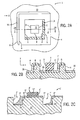
- FIG. 1A shows an enlarged schematic top view of a conventional box-in-box registration structure.
- FIG. 1B shows an enlarged schematic cross-sectional view taken along line 1 B— 1 B of FIG. 1 A.
- FIG. 2A shows an enlarged schematic top view of a box-in-box registration structure comprising an asymmetrically deposited material layer.
- FIG. 2B shows an enlarged schematic cross-sectional view taken along line 2 B— 2 B of FIG. 2 A.
- FIG. 2C shows another embodiment of a registration measurement structure comprising a recessed component and an asymmetrically deposited film layer
- FIG. 3A shows an enlarged schematic top view of a box-in-box registration structure 6 comprising an asymmetrically deposited material layer.
- FIG. 3B shows an enlarged schematic cross-sectional view taken along line 3 B— 3 B of FIG. 3 A.
- FIG. 3C shows a pair of enlarged measurement gate images of the outer box of the box-in-box registration structure of FIGS. 3A-3B comprising an asymmetric deposition layer.
- FIG. 3D shows a pair of enlarged measurement gate images of the outer box of the box-in-box registration structure of FIGS. 3A-3B comprising an asymmetric deposition layer, the pair of images rotated with respect to the images of FIG. 3 C.
- FIG. 3E shows a pair of enlarged measurement gate images of the outer box of the box-in-box registration structure of FIGS. 3A-3B comprising an asymmetric deposition layer, one of the images rotated with respect to the images of FIG. 3 C.
- the terms “semiconductive wafer fragment” or “wafer fragment” or “wafer” will be understood to mean any construction comprising semiconductor material, including but not limited to bulk semiconductive materials such as a semiconductor wafer (either alone or in assemblies comprising other materials thereon), and semiconductive material layers (either alone or in assemblies comprising other materials).
- substrate refers to any supporting structure including, but not limited to, the semiconductive wafer fragments br wafers described above.
- a conventional registration measurement structure comprises a “box-in-box” overlay structure (also called a “target” or “site”) that typically comprises two or more overlay components (marks), and represents or describes the overlay of a given material layer with respect to a previously deposited material layer at a single site (also called a “point” or “location”) on a readable field of a wafer.
- Such registration measurement structures are repeated at various points across the wafer.
- significant information can be obtained at each site, for instance, by measuring or at least two different directions (e.g., in a typical Cartesian coordinate system, measuring in an “x” and a “y” direction). Information or data can be obtained in this manner across an entire silicon wafer.
- This data can then be analyzed, modeled, or otherwise manipulated so as to accomplish various tasks, such as, for example, to reduce or remove overlay error and achieve proper registration of a subsequently deposited layer with respect to previous layers.
- overlay error can be caused by certain tooling or IC fabrication processes.
- An imaging tool e.g., an optical system
- an autofocus mechanism e.g., a laser focusing system
- a specialized optical microscope e.g., a laser focusing system
- One registration tool suitable for use with respect to the present invention is an IVS registration tool (e.g., the IVS- 120 optical metrology tool) available from Schlumberger Automated Test Equipment (ATE), located in San Jose, Calif.
- ATE Schlumberger Automated Test Equipment
- the tool includes an adaptive RG software algorithm that provides the capability to measure targets using images of the targets that are created by the image sensing and optical apparatuses in the registration tool.
- KLA-Tencor Corporation located in San Jose, Calif., also manufacturers a variety of suitable registration software packages, sold under the brand name KLASSTM.
- Registration tools can detect a position of overlay marks that make up, for example, a box-in-box registration structure on a substrate.
- the registration tool typically images the substrate and registration structure(s) using an optical system which can include a radiation source and a radiation detector (neither of which is shown) to produce a registration signal that is processed by a processor (also not shown).
- Imaging of the registration structure on the substrate can be accomplished by capturing two-dimensional or three-dimensional images of the registration structure using an image detector (not shown), such as a charge coupled device (CCD) camera so as to provide data of the registration structure to the processor.
- CCD charge coupled device
- the processor utilized in conjunction with the registration tool can comprise a microprocessor, an Application-Specific Integrated Circuit (ASIC), or any other combination of hardware and or/or software. It will also be understood by those of skill in the art that the processor can be designed as part of an existing processor of a registration tool, or alternatively, as a stand-alone processor.
- ASIC Application-Specific Integrated Circuit
- Registration is typically obtained by imaging registration measurement structures generally comprising components (marks) on a substrate.
- substrates comprise silicon, silicon nitride, silicon dioxide, silicon carbide, gallium arsenide or other semiconductor material.
- the registration measurement structure comprises a first component in a first or lower layer of a semiconductor construction, and a second component in an overlying second or upper layer.
- the registration tool then typically determines, based on the image and/or reference points on the first component, the relative position of the second component of the registration measurement structure. It then creates a signal based on that image or reference points.
- the second component is symmetrically positioned with respect to the first component, and its center position is well defined.
- metal deposition processes can result in an asymmetric layer being deposited onto the first component of the registration measurement structure, resulting in an inaccurate or false measurement being taken of the registration structure.
- the false measurement is then sent as a signal to the patterning apparatus, even though the second component itself may be symmetrically positioned. Due to the registration error caused by the asymmetric film deposition on the first component of the registration structure, it can be difficult to determine a center position of the second component.
- FIGS. 1A-1B a first embodiment of the invention is described with reference to a method of reducing registration error caused by asymmetrical deposition processes.
- a first component 2 comprising a larger box formed as raised area or “mesa”, in the shape of a square is formed over or in a substrate layer 10 .
- Raised first component 2 comprises a top edge 11 .
- a second component 4 comprising a smaller box comprising a photoresist layer is formed as a top layer 12 over the larger box 2 and substrate 10 to correspond with the first component 2 .
- the photoresist layer can comprise a variety of photosensitive polymeric materials for example, a novalac resin.
- the first component 2 of the registration structure 1 can be a raised structure such as a mesa that is formed in a substrate 10 .
- the first component 2 ′ can also be a recessed structure or trench etched into a substrate layer 10 ′.
- the first component 2 can be formed to be about 1 to about 4 microns ( ⁇ m) wide, or more preferably, about 2 to about 4 microns ( ⁇ m) wide.
- the height of the first component 2 is typically about 0.1 to about 0.5 microns ( ⁇ m) or more preferably about 0.3 to about 0.5 microns ( ⁇ m).
- the above-described dimensions can vary widely depending on the specific application and are provided by way of example only.
- a registration measurement structure 1 can vary to convenience depending on the application at hand.
- suitable shapes for the registration measurement structure can include crosses chevrons, among others.
- the registration structure can be made according to well-known, conventional fabrication processes.
- the registration measurement structure 1 is shown without a material layer ( 16 ) deposited over the first component 2 of the structure.
- the upper box (second component) 4 appears to be in alignment (i.e., registration) with the lower box (first component) 2 .
- distances such as height and width can be determined by measuring distances between edges (or other reference point) on the registration measurement structure. Such distances are referred to herein as “critical dimensions”.
- edges A through H of the registration measurement structure can be perceived or recognized by an imaging device, and thus measured, by a registration tool (not shown).
- the first component 2 of the registration structure comprises first and second edges B and C
- the second component 4 comprises first and second edges D and E
- the asymmetric film layer comprises an edge A.
- Registration error if any, between the overlay of the upper box (second component) 4 with respect to the lower box (first component) 2 , can be obtained by determining the distance from edge C to edge D (referred to as “CD”) and the distance from edge E to edge F, (referred to as “EF”). These distances can be compared, and the error can be substantially accounted for by the following subtraction one distance from the other, for example, distance CD minus distance EF (i.e., CD-EF).
- metal deposition can result in an asymmetric layer 16 being deposited onto the first component (mesa) 2 of registration structure 1 , and more specifically over certain portions of its topography, e.g., the metal process films or layers deposited onto certain edges of the first component (mesa) 2 .
- the deposited film can be thicker on one side of the first component (mesa) 2 than the other side.
- Registration tools typically measure the registration structure from an edge to a centerline (or vice versa).
- a metal film 16 is typically deposited downwardly and at angle onto the substrate, in a set direction such as from left to right across the surface, or in radial fashion.
- a deposited metal film 16 generally appears opaque to the imaging mechanism of a registration tool. As such, the registration tool cannot detect the true edges of the registration structure 2 through the opaque film, but images or measures the apparent edges of the registration structure 2 that includes an overlying film layer 16 .
- the perceived (i.e., measured) edges A, C, D, E, F and H measured by a registration tool can be effectively offset by an amount corresponding to the thickness (width) of the film layer 16 as measured from edge A to edge B, which is contiguous to a reference edge (C) of the first component (trench, mesa) 2 of the registration structure.
- the registration tool images and transmits a registration signal of the registration structure 1 to a processor (not shown), with the registration signal including the offset amount due to the asymmetric deposition of the film layer 16 .
- a subsequently deposited material layer (not shown), can be misaligned with respect to an underlying material layer.
- the first component (raised area or mesa) 2 is defined, at least in part, by edges B, C, G and H.
- the second component 4 exemplified by a photoresist layer, is formed onto a film layer 16 (e.g., metal) that has been asymmetrically deposited over the first component 2 .
- the second component 4 is defined, at least in part, by edges D and E.
- the deposition of the film layer 16 can result in a build-up of material along one side of the first component 2 . This forms asymmetric deposition edges “A” and “F”, which are edges of the deposited material 16 that is contiguous with edges B and G of the first component.
- edges of the registration measurement structure can be perceived or recognized, and thus measured, by a registration tool (not shown).
- measurable edges include asymmetric deposition edges A and F, and edges C, D, E, and H of the first and second components of the registration measurement structure.
- Edges B and G of the first component 2 of the registration structure cannot be perceived or measured using the registration tool due to the generally opaque asymmetric film layer 16 that is deposited over these edges.
- the amount of the false registration measurement corresponds to the thickness of the asymmetric layer 16 contiguous to the edge B of the first component 2 of the registration structure, which can be represented by the distance from edge A of the asymmetric layer 16 to edge B of the first component 2 (i.e., distance AB), or alternatively—because of structure symmetry—the distance between edges F and G of the asymmetric layer 16 and the first component 2 of the second depicted registration structure (i.e., distance FG).
- the width of the first component 2 can be obtained according to the known (or predetermined) dimensions of the pattern (e.g., mask or reticle) used in forming the first component 2 .
- Dimension AC can also be determined by measuring and/or experimental sampling of registration structure components using methods known to those of skill in the art. Such critical dimensions can be measured using a registration tool or Critical Dimension Scanning Electron Microscope. As a practical matter, such a determination can desirably take place prior to asymmetric deposition of the metal layer. Measuring critical dimensions introduces error into the final overlay of one material layer to a subsequent material layer. However, such error is significantly less than the error that typically would result if the error due to asymmetric film deposition is not accounted for (i.e., the error to asymmetric film deposition is assumed to be negligible or zero).
- the true or actual registration error due to asymmetric deposition (or amount of the registration offset corresponding to the thickness of the asymmetric deposition on the edge of the first component of the registration structure) can be calculated.
- the registration error due to asymmetric deposition of the film layer 16 can be calculated as the difference between the magnitude of critical dimension (distance) AC and the magnitude of critical dimension (distance) BC, or simply, distance AC minus distance BC (i.e., AC ⁇ BC). This, of course, corresponds to the distance AB. Since the box-in-box registration measurement structure 1 that is shown is itself symmetrical, the offset or overlay error of the second component 4 relative to the first component 2 is equal to half the magnitude of the critical dimension (distance) BC (i.e., BC/2).
- an actual registration value for the registration measurement structure 1 comprising an asymmetric deposition layer 16 can be determined. This actual value can be conveyed to a patterning apparatus to align a subsequent layer onto the substrate.
- the amount of asymmetric deposition corresponding to the thickness of the deposition layer 16 can vary across the surface of the substrate.
- the amount of asymmetric deposition is preferably measured, modeled and corrected for at each registration measurement structure (e.g., the box-in-box registration structure illustrated in here) across the wafer. That is, each structure 1 , and each corresponding error determination, can be considered as a point. This process can be continuing, point-by-point, across a substrate.
- the points can be collected to create a data set. From this data set, an overall alignment error for overlying patterned layers of an IC can be determined and/or modeled, and overall alignment of the layers can be achieved.
- a key feature of this invention is that the critical dimension determinations are utilized to obtain an error or offset amount due to asymmetric film deposition.
- the offset amount can be conveyed to a patterning apparatus. Such error can be effectively subtracted out of or removed from the overall registration for a structure and, by continuing the process, across a wafer substrate.
- the registration measurement structure 1 ′ can comprise a first component 2 ′ in the form of a recessed structure of trench. As shown, a film layer 16 ′ has been asymmetrically deposited over the edge B′ of the trench-structured first component 2 ′. Measurements can be taken with respect to edges A′ through H′ of the registration measurement structure 1 ′ to determine and resolve the registration error in the alignment of the first and second components 2 ′, 4 ′, according to the method as described with respect to FIGS. 2A-2B .
- FIGS. 3A-3C a second embodiment of a method according to the invention is described with reference to imaging a pair of gate images of a reference measurement structure to provide for improved site registration, or reduced (and potentially eliminated) registration error caused by asymmetrical deposition processes.
- a film layer (metal material) 16 is deposited onto a wafer substrate, for example, to create metal interconnects or other IC elements, components (which can, alone or in combination with other components, make up a registration measurement structure) are used to accomplish registration.
- the true or actual centerline of the exemplary box-in-box registration structure 1 ′′ is indicated by solid line 30 ′′.
- the deposition of the material layer 16 ′′ can cause mis-registration between the outer box component 2 ′′ and the inner box component 4 ′′; which ultimately can result in the misalignment of overlying patterned layers by the amount by which the perceived or apparent site line is offset from the actual or true centerline 30 ′′ of the registration structure.
- left and right image gates X 1 , X 2 are shown to overlie the first component 2 ′′ comprising a raised, larger outer box, of the registration structure 1 ′′.
- Image gates Y 1 and Y 2 are shown to overlie edges D′′ and E′′ of the second component 2 ′′ comprising the second component 4 ′′ comprising an inner, smaller box comprising, for example, a photoresist layer.
- a registration tool uses image gates X 1 , X 2 , Y 1 and Y 2 to determine where the centerline 30 ′′ of the outer and inner boxes 2 ′′, 4 ′′ of the registration structure 1 ′′ are located.
- a registration tool can be used to obtain the gate images by taking a contrast images (e.g., a CCD photograph).
- the registration measurement structure 1 ′′ comprises a first component (mark) 2 ′′, which is formed in a lower substrate layer 10 ′′ using standard IC fabrication techniques, such as resist pattern and etch.
- the registration measurement structure 1 ′′ further comprises a second component (mark) 4 ′′ as a top or current layer, shown here as a photoresist layer.
- the first and second components 2 ′′, 4 ′′ are shown as identical or substantially identical in shape (i.e., as rectangles), thereby creating a symmetrical box-in-box design.
- an exemplary “ideal” registration measurement structure 1 ′′ is shown. It will be recognized and understood by those of skill in the art that the registration structure can be fabricated using known but imperfect manufacturing processes, which lead to imperfections in its shape.
- gate images enlarged schematic images (referred to herein as “gate images”) of registration structure 1 ′′ comprising the outer box (first component) portions 2 a ′′, 2 b ′′, and asymmetrically deposited film layer portions 16 a ′′ and 16 b ′′ are illustrated. More specifically, a pair of gate images I 1 and I 2 (as shown, left and right) can be used to determine the position of sides or edges of the illustrated box-in-box registration measurement structure.
- asymmetric film deposition layer portions 16 a ′′, 16 b ′′ cause the registration tool to image the apparent centerline of outer box portion 2 a ′′ with deposition layer portion 16 a ′′ thereon as an offset line 31 ′′, and the apparent centerline of outer box portion 2 b ′′ with deposition layer portion 16 a ′′ thereon as an offset line 32 ′′.
- This registers the apparent centerline of the overall box-in-box structure 1 ′′ (i.e. site center) as an offset or site line 33 ′′.
- the registration tool accomplishes this determination by imaging a pair of images I 1 and I 2 of the outer box (first) component 2 ′′ of the registration structure, and determining a value of the apparent centerlines of each of the images I 1 and I 2 of the first material layer or component 2 ′′.
- the image centerline values are then averaged to provide a site line 33 ′′, or first offset centerline value.
- a pair of images delineated by the image gates Y 1 and Y 2 (not depicted) are also taken of the inner box (second) component 4 ′′ of the registration structure, and a value of the apparent centerlines of each of the images of the second material layer or component 4 ′′ are determined.
- the image centerline values of the second material layer images are then averaged to provide a second offset centerline value.
- the first offset centerline value is then compared with the second offset centerline value to provide a first delta value ( ⁇ 1 ), referred to as “site-induced-shift”.
- site-induced-shift Such registration measurements can be taken for each registration structure 1 ′′ across a wafer, and a data set created.
- the registration tool can electronically rotate or flip one or both of the gate images I 1 , I 2 of the portions of the outer box components 2 a ′′, 2 b ′′, resulting in the image pairs shown in FIGS. 3D and 3E .
- both gate images I 1 , I 2 have been electronically flipped by the registration tool, resulting in flipped images I 1F , I 2F .
- each of the images have been flipped 180° about a central axis 40 a ′′, 40 b ′′ ( FIGS. 3A-3B ) of the image gates.
- the registration tool measures the apparent centerlines 34 ′′ and 35 ′′, respectively, of the outer box components 2 a ′′, 2 b ′′ so as to determine the amounts that the apparent centerlines 34 ′′ and 35 ′′ are offset from the true centerline 30 ′′.
- the image centerline values 34 ′′, 35 ′′ of the flipped images I 1F , I 2F , of the first material layer or component 2 ′′ are then determined and averaged to provide a site line 36 ′′, or third offset centerline value.
- the third offset center line value is then compared to the second offset centerline value to provide a second delta value ( ⁇ 2 ).
- the ⁇ 1 value is then subtracted from the ⁇ 2 value to provide a ⁇ s value, which is then averaged to provide a registration measurement error, which corresponds to the offset amount due to the asymmetric deposition of the film layer portions 16 a ′′, 16 b ′′.
- a registration measurement error corresponds to the offset amount due to the asymmetric deposition of the film layer portions 16 a ′′, 16 b ′′.
- the greater the averages ⁇ s value the greater the asymmetry of the film layer over the outer box component portions 2 a ′′, 2 b ′′.
- the registration measurement error is then subtracted from the registration structure centerline value to generate a corrected data representative of an actual centerline value of the registration structure.
- the actual centerline value of the registration structure is then conveyed to a patterning apparatus to align a subsequently patterned layer.
- the sputter (or other metal deposition process) tool applies the metal or other material layer in a manner that introduces a radial asymmetry to the deposited film layer 16 ′′.
- the sputter (or other metal deposition process) tool applies the metal or other material layer in a manner that introduces a radial asymmetry to the deposited film layer 16 ′′.
- an excess amount of material can be deposited onto one side of the wafer substrate resulting in a build-up of material along one side of the lower component 2 ′′ of a registration mark.
- the position of the raised feature 2 ′′ appears to be closer toward the wafer center than its actual position.
- Wafer magnification can be corrected or accounted for by entering a wafer magnification factor into the exposure tool to change the exposure tool stepping distance between field images.
- only one of two gate images e.g., I 1 or I 2
- I 1 or I 2 is electronically rotated or flipped onto itself, as shown in FIGS. 3C and 3E .
- I 2 FIG. 3C
- I 2F flipped image
- a pair of images I 1 , I 2 of the outer box (first component) 2 ′′ of the registration structure 1 ′′ are again obtained (FIG. 3 C), and an image centerline value 37 ′′, 38 ′′ for each of the images I 1 , I 2 is determined and averaged to provide a first offset centerline value.
- a pair of images delineated by the image gates Y 1 and Y 2 ( FIG. 3A ) are also again taken of the inner box (second) component 4 ′′ of the registration structure, and a value of the apparent centerlines of each of the images of the second material layer or component 4 ′′ are determined and averaged to provide a second offset centerline value.
- the first and second offset centerline values are then compared to provide a first delta value ( ⁇ 1 ).
- image I 2 of the outer box (first) component 2 ′′ has been flipped/rotated resulting in a flipped image I 2F and a non-flipped image I 1 , as shown in FIG. 3 E.
- the registration tool can measure the respective apparent centerlines, 37 ′′ and 38 ′′ of the flipped image I 2F and a non-flipped image I 1 of the outer box component portions 2 a ′′, 2 b ′′ and average the values to provide a site line 39 ′′, or third offset centerline value.
- the third offset center line value is then compared to the second offset centerline value to provide a second delta value ( ⁇ 2 ).
- the ⁇ 1 value is then subtracted from the ⁇ 2 value to provide a ⁇ s value which corresponds to a registration measurement error due to the asymmetric deposition of the film layer portions 16 a ′′, 16 b ′′.
- the registration measurement error is then subtracted from the registration structure centerline value to generate a corrected data representative of an actual centerline value of the registration structure.
- the actual centerline value is then conveyed to a patterning apparatus to align a subsequently patterned layer relative to the registration structure and the component 4 ′′.
- Field magnification results when the image-sensing mechanism or apparatus magnifies a field comprising a plurality of registration structures or sites. Field magnification can be corrected or accounted for by a field magnification factor that can be entered into the exposure tool to reduce or increase the field magnification as needed.
- two measurements are taken. First, non-flipped gate image measurements are taken. Then, ether one gate image (e.g., I 1 , or I 2 ) is flipped and measured, or both gate images (e.g., I 1 and I 2 ) are flipped and measured.
- gate images e.g., wafer magnification, field magnification, and translational shifts
- two measurements are taken. First, non-flipped gate image measurements are taken. Then, ether one gate image (e.g., I 1 , or I 2 ) is flipped and measured, or both gate images (e.g., I 1 and I 2 ) are flipped and measured.
- a pair of images I 1 , I 2 of the outer box (first component 2 ′′) are obtained (FIG. 3 C), and one of the pair of images is manipulated resulting in a first flipped image and a non-flipped image. Apparent image centerline values of the flipped and non-flipped images are determined and averaged to provide a first offset centerline value.
- a pair of images of the inner box (second component) 4 ′′ of the registration structure 1 ′′ are then obtained as described herein, and apparent image centerline values of each of the images of the inner box component) 4 ′′ are then determined and averaged to provide a second offset centerline value.
- the first and second offset centerline values are then compared to provide a first delta value ( ⁇ 1 ).
- the other (non-flipped) image of the outer box component 2 ′′ is then flipped/rotated to provide a pair of flipped gate images I 1F , I 2F , and the image centerline values of the flipped images are determined and averaged to provide a third offset centerline value.
- the third offset centerline value is then compared to the second offset centerline value to provide a second delta value ( ⁇ 2 ).
- the ⁇ 1 value is then subtracted from the ⁇ 2 value to provide a ⁇ 3 value corresponding to a registration measurement error, which is then subtracted from the registration structure centerline value to generate a corrected data representative of an actual centerline value of the registration structure.
- This actual centerline value of the registration structure can then be electronically transmitted to a patterning apparatus to align a subsequently patterned layer relative to the registration structure.
- the present layer-to-layer overlay metrology can be used to measure the alignment accuracy between a photoresist layer and an underlying substrate layer, and also to determine the alignment accuracy of a photoresist mask for etching a substrate material and, if necessary, the photoresist can be removed or reworked.
- the methods and illustrations provided herein support combinations of means of performing the specified functions, combinations of steps (i.e., one such combination comprising a single step, another such combination comprising two or more steps) for performing the specified functions and program instruction means for performing the specified functions. It will also be understood that each method can be implemented by special purpose hardware-based systems, such as the kind described above or other conventional systems, which can perform the specified functions or steps as described above and/or by combinations of special purpose hardware and computer instructions.
- Overlay metrology is performed to determine how well one layer overlays to a previous layer.
- metrology compares a registration mark, generally referred to as a metrology mark, on a current layer with an registration mark on a previous layer.
- the registration or metrology tool detects the registration marks and determines the positions of the current and previous registration marks. From these positions, an overlay offset can be calculated. Accordingly, the present invention can be used to detect the positions of the current and previous overlay marks during the metrology phase.
- the present invention is described in the context of metal deposition processes, such as sputtering, it will be understood that the invention can apply to any film that can be deposited to have a varying thickness from one side of a feature (e.g., a transoral line, a pattern, etc.), or, from the center to the edge of, for example, a wafer.
- a feature e.g., a transoral line, a pattern, etc.
Abstract
Description
Claims (42)
Priority Applications (1)
| Application Number | Priority Date | Filing Date | Title |
|---|---|---|---|
| US10/122,555 US6852456B2 (en) | 2001-03-23 | 2002-04-15 | Reducing asymmetrically deposited film induced registration error |
Applications Claiming Priority (2)
| Application Number | Priority Date | Filing Date | Title |
|---|---|---|---|
| US09/816,861 US6486956B2 (en) | 2001-03-23 | 2001-03-23 | Reducing asymmetrically deposited film induced registration error |
| US10/122,555 US6852456B2 (en) | 2001-03-23 | 2002-04-15 | Reducing asymmetrically deposited film induced registration error |
Related Parent Applications (1)
| Application Number | Title | Priority Date | Filing Date |
|---|---|---|---|
| US09/816,861 Division US6486956B2 (en) | 2001-03-23 | 2001-03-23 | Reducing asymmetrically deposited film induced registration error |
Publications (2)
| Publication Number | Publication Date |
|---|---|
| US20020137303A1 US20020137303A1 (en) | 2002-09-26 |
| US6852456B2 true US6852456B2 (en) | 2005-02-08 |
Family
ID=25221798
Family Applications (4)
| Application Number | Title | Priority Date | Filing Date |
|---|---|---|---|
| US09/816,861 Expired - Lifetime US6486956B2 (en) | 2001-03-23 | 2001-03-23 | Reducing asymmetrically deposited film induced registration error |
| US10/122,555 Expired - Fee Related US6852456B2 (en) | 2001-03-23 | 2002-04-15 | Reducing asymmetrically deposited film induced registration error |
| US10/122,786 Expired - Fee Related US6795747B2 (en) | 2001-03-23 | 2002-04-15 | Reducing asymmetrically deposited film induced registration error |
| US10/932,771 Expired - Lifetime US7127319B2 (en) | 2001-03-23 | 2004-09-02 | Reducing asymmetrically deposited film induced registration error |
Family Applications Before (1)
| Application Number | Title | Priority Date | Filing Date |
|---|---|---|---|
| US09/816,861 Expired - Lifetime US6486956B2 (en) | 2001-03-23 | 2001-03-23 | Reducing asymmetrically deposited film induced registration error |
Family Applications After (2)
| Application Number | Title | Priority Date | Filing Date |
|---|---|---|---|
| US10/122,786 Expired - Fee Related US6795747B2 (en) | 2001-03-23 | 2002-04-15 | Reducing asymmetrically deposited film induced registration error |
| US10/932,771 Expired - Lifetime US7127319B2 (en) | 2001-03-23 | 2004-09-02 | Reducing asymmetrically deposited film induced registration error |
Country Status (1)
| Country | Link |
|---|---|
| US (4) | US6486956B2 (en) |
Cited By (1)
| Publication number | Priority date | Publication date | Assignee | Title |
|---|---|---|---|---|
| US20050181571A1 (en) * | 2004-02-18 | 2005-08-18 | Jack Lin | Method and apparatus for forming patterned photoresist layer |
Families Citing this family (15)
| Publication number | Priority date | Publication date | Assignee | Title |
|---|---|---|---|---|
| US6440612B1 (en) | 1999-09-01 | 2002-08-27 | Micron Technology, Inc. | Field correction of overlay error |
| JP2003031477A (en) * | 2001-07-17 | 2003-01-31 | Hitachi Ltd | Manufacturing method of semiconductor device and system thereof |
| JP2003224057A (en) * | 2002-01-30 | 2003-08-08 | Hitachi Ltd | Method of manufacturing semiconductor device |
| US6778275B2 (en) | 2002-02-20 | 2004-08-17 | Micron Technology, Inc. | Aberration mark and method for estimating overlay error and optical aberrations |
| US6701206B1 (en) * | 2002-05-03 | 2004-03-02 | Advanced Micro Devices, Inc. | Method and system for controlling a process tool |
| US7065737B2 (en) * | 2004-03-01 | 2006-06-20 | Advanced Micro Devices, Inc | Multi-layer overlay measurement and correction technique for IC manufacturing |
| US7192845B2 (en) * | 2004-06-08 | 2007-03-20 | Macronix International Co., Ltd. | Method of reducing alignment measurement errors between device layers |
| US7463367B2 (en) * | 2004-07-13 | 2008-12-09 | Micron Technology, Inc. | Estimating overlay error and optical aberrations |
| KR100568729B1 (en) * | 2004-12-02 | 2006-04-07 | 삼성전자주식회사 | Structure for protecting a region in which an overlay mark is formed, overlay mark having the structure and method of forming the overlay mark |
| US7615404B2 (en) * | 2006-10-31 | 2009-11-10 | Intel Corporation | High-contrast laser mark on substrate surfaces |
| US8148682B2 (en) * | 2009-12-29 | 2012-04-03 | Hitachi, Ltd. | Method and apparatus for pattern position and overlay measurement |
| KR101675380B1 (en) * | 2010-02-19 | 2016-11-14 | 삼성전자주식회사 | method for correcting overlay and manufacturing method of semiconductor device used the same |
| CN103003754B (en) * | 2010-07-19 | 2015-03-11 | Asml荷兰有限公司 | Method and apparatus for determining an overlay error |
| US9506965B2 (en) * | 2012-11-12 | 2016-11-29 | United Microelectronics Corp. | Alternately arranged overlay marks having asymmetric spacing and measurement thereof |
| KR102517587B1 (en) | 2019-07-10 | 2023-04-03 | 케이엘에이 코포레이션 | Data-based misalignment parameter configuration and measurement system and method |
Citations (20)
| Publication number | Priority date | Publication date | Assignee | Title |
|---|---|---|---|---|
| US4794646A (en) | 1985-08-14 | 1988-12-27 | Mitsubishi Denki Kabushiki Kaisha | Charged beam pattern defect inspection apparatus |
| US5057689A (en) | 1989-09-20 | 1991-10-15 | Matsushita Electric Industrial Co., Ltd. | Scanning electron microscope and a method of displaying cross sectional profiles using the same |
| US5414519A (en) | 1991-04-12 | 1995-05-09 | Goldstar Electron Co., Ltd. | Method for aligning a semiconductor chip to be repaired with a repair system and a laser repair target used therefor |
| US5498500A (en) | 1993-12-27 | 1996-03-12 | Hyundai Electronics Industries Co., Ltd. | Overlay measurement mark and method of measuring an overlay error between multi patterns in a semiconductor device using the measurement mark |
| US5602492A (en) | 1992-03-13 | 1997-02-11 | The United States Of America As Represented By The Secretary Of Commerce | Electrical test structure and method for measuring the relative locations of conducting features on an insulating substrate |
| US5617340A (en) | 1994-04-28 | 1997-04-01 | The United States Of America As Represented By The Secretary Of Commerce | Method and reference standards for measuring overlay in multilayer structures, and for calibrating imaging equipment as used in semiconductor manufacturing |
| US5641960A (en) | 1994-01-13 | 1997-06-24 | Fujitsu Limited | Circuit pattern inspecting device and method and circuit pattern arrangement suitable for the method |
| US5659172A (en) | 1995-06-21 | 1997-08-19 | Opal Technologies Ltd. | Reliable defect detection using multiple perspective scanning electron microscope images |
| US5699282A (en) | 1994-04-28 | 1997-12-16 | The United States Of America As Represented By The Secretary Of Commerce | Methods and test structures for measuring overlay in multilayer devices |
| US5857258A (en) | 1992-03-13 | 1999-01-12 | The United States Of America As Represented By The Secretary Of Commerce | Electrical test structure and method for measuring the relative locations of conductive features on an insulating substrate |
| US5953128A (en) * | 1997-08-28 | 1999-09-14 | International Business Machines Corporation | Optically measurable serpentine edge tone reversed targets |
| US5965309A (en) * | 1997-08-28 | 1999-10-12 | International Business Machines Corporation | Focus or exposure dose parameter control system using tone reversing patterns |
| US6033582A (en) * | 1996-01-22 | 2000-03-07 | Etex Corporation | Surface modification of medical implants |
| US6040618A (en) | 1997-03-06 | 2000-03-21 | Micron Technology, Inc. | Multi-chip module employing a carrier substrate with micromachined alignment structures and method of forming |
| US6050279A (en) * | 1998-06-08 | 2000-04-18 | Advanced Micro Devices, Inc. | Apparatus and method for immersing an object in a liquid such that a lower surface of the object does not touch a bottom surface of a container holding the liquid |
| US6064486A (en) | 1998-05-21 | 2000-05-16 | Leland Stanford Junior University | Systems, methods and computer program products for detecting the position of a new alignment mark on a substrate based on fitting to sample alignment signals |
| US6077756A (en) | 1998-04-24 | 2000-06-20 | Vanguard International Semiconductor | Overlay target pattern and algorithm for layer-to-layer overlay metrology for semiconductor processing |
| US6091845A (en) | 1998-02-24 | 2000-07-18 | Micron Technology, Inc. | Inspection technique of photomask |
| US6137578A (en) * | 1998-07-28 | 2000-10-24 | International Business Machines Corporation | Segmented bar-in-bar target |
| US6143629A (en) * | 1998-09-04 | 2000-11-07 | Canon Kabushiki Kaisha | Process for producing semiconductor substrate |
-
2001
- 2001-03-23 US US09/816,861 patent/US6486956B2/en not_active Expired - Lifetime
-
2002
- 2002-04-15 US US10/122,555 patent/US6852456B2/en not_active Expired - Fee Related
- 2002-04-15 US US10/122,786 patent/US6795747B2/en not_active Expired - Fee Related
-
2004
- 2004-09-02 US US10/932,771 patent/US7127319B2/en not_active Expired - Lifetime
Patent Citations (20)
| Publication number | Priority date | Publication date | Assignee | Title |
|---|---|---|---|---|
| US4794646A (en) | 1985-08-14 | 1988-12-27 | Mitsubishi Denki Kabushiki Kaisha | Charged beam pattern defect inspection apparatus |
| US5057689A (en) | 1989-09-20 | 1991-10-15 | Matsushita Electric Industrial Co., Ltd. | Scanning electron microscope and a method of displaying cross sectional profiles using the same |
| US5414519A (en) | 1991-04-12 | 1995-05-09 | Goldstar Electron Co., Ltd. | Method for aligning a semiconductor chip to be repaired with a repair system and a laser repair target used therefor |
| US5602492A (en) | 1992-03-13 | 1997-02-11 | The United States Of America As Represented By The Secretary Of Commerce | Electrical test structure and method for measuring the relative locations of conducting features on an insulating substrate |
| US5857258A (en) | 1992-03-13 | 1999-01-12 | The United States Of America As Represented By The Secretary Of Commerce | Electrical test structure and method for measuring the relative locations of conductive features on an insulating substrate |
| US5498500A (en) | 1993-12-27 | 1996-03-12 | Hyundai Electronics Industries Co., Ltd. | Overlay measurement mark and method of measuring an overlay error between multi patterns in a semiconductor device using the measurement mark |
| US5641960A (en) | 1994-01-13 | 1997-06-24 | Fujitsu Limited | Circuit pattern inspecting device and method and circuit pattern arrangement suitable for the method |
| US5617340A (en) | 1994-04-28 | 1997-04-01 | The United States Of America As Represented By The Secretary Of Commerce | Method and reference standards for measuring overlay in multilayer structures, and for calibrating imaging equipment as used in semiconductor manufacturing |
| US5699282A (en) | 1994-04-28 | 1997-12-16 | The United States Of America As Represented By The Secretary Of Commerce | Methods and test structures for measuring overlay in multilayer devices |
| US5659172A (en) | 1995-06-21 | 1997-08-19 | Opal Technologies Ltd. | Reliable defect detection using multiple perspective scanning electron microscope images |
| US6033582A (en) * | 1996-01-22 | 2000-03-07 | Etex Corporation | Surface modification of medical implants |
| US6040618A (en) | 1997-03-06 | 2000-03-21 | Micron Technology, Inc. | Multi-chip module employing a carrier substrate with micromachined alignment structures and method of forming |
| US5953128A (en) * | 1997-08-28 | 1999-09-14 | International Business Machines Corporation | Optically measurable serpentine edge tone reversed targets |
| US5965309A (en) * | 1997-08-28 | 1999-10-12 | International Business Machines Corporation | Focus or exposure dose parameter control system using tone reversing patterns |
| US6091845A (en) | 1998-02-24 | 2000-07-18 | Micron Technology, Inc. | Inspection technique of photomask |
| US6077756A (en) | 1998-04-24 | 2000-06-20 | Vanguard International Semiconductor | Overlay target pattern and algorithm for layer-to-layer overlay metrology for semiconductor processing |
| US6064486A (en) | 1998-05-21 | 2000-05-16 | Leland Stanford Junior University | Systems, methods and computer program products for detecting the position of a new alignment mark on a substrate based on fitting to sample alignment signals |
| US6050279A (en) * | 1998-06-08 | 2000-04-18 | Advanced Micro Devices, Inc. | Apparatus and method for immersing an object in a liquid such that a lower surface of the object does not touch a bottom surface of a container holding the liquid |
| US6137578A (en) * | 1998-07-28 | 2000-10-24 | International Business Machines Corporation | Segmented bar-in-bar target |
| US6143629A (en) * | 1998-09-04 | 2000-11-07 | Canon Kabushiki Kaisha | Process for producing semiconductor substrate |
Non-Patent Citations (3)
| Title |
|---|
| Aronson, Arnold J., Fundamentals of Sputtering, Microelectronic Manufacturing and Testing, Jan. 1987, vol. 10, No. 1, pp. 22-23. |
| Van Zant, Peter, Microchip Fabrication: A Practical Guide to Semiconductor Processing, Fourth Edition, 2000, pp. 411-416. |
| Wolf, Stanley, et al., Aluminum Thin Films and Physical Vapor Deposition in ULSI, Silicon Processing for the VLSI Era, vol. 1: Process Technology, Second Edition, Chapter 11, pp. 434-487, 2000. |
Cited By (2)
| Publication number | Priority date | Publication date | Assignee | Title |
|---|---|---|---|---|
| US20050181571A1 (en) * | 2004-02-18 | 2005-08-18 | Jack Lin | Method and apparatus for forming patterned photoresist layer |
| US7033903B2 (en) * | 2004-02-18 | 2006-04-25 | United Microelectronics Corp. | Method and apparatus for forming patterned photoresist layer |
Also Published As
| Publication number | Publication date |
|---|---|
| US20020137303A1 (en) | 2002-09-26 |
| US20050027388A1 (en) | 2005-02-03 |
| US6795747B2 (en) | 2004-09-21 |
| US7127319B2 (en) | 2006-10-24 |
| US20020137237A1 (en) | 2002-09-26 |
| US20020137240A1 (en) | 2002-09-26 |
| US6486956B2 (en) | 2002-11-26 |
Similar Documents
| Publication | Publication Date | Title |
|---|---|---|
| US6852456B2 (en) | Reducing asymmetrically deposited film induced registration error | |
| US5868560A (en) | Reticle, pattern transferred thereby, and correction method | |
| KR0170909B1 (en) | Overlay detecting method of semiconductor device | |
| JP2002093699A (en) | Overlay registration error measurement carried out for more than two semiconductor wafer layers at the same time | |
| US6484060B1 (en) | Layout for measurement of overlay error | |
| US7449792B2 (en) | Pattern registration mark designs for use in photolithography and methods of using the same | |
| JP4235459B2 (en) | Alignment method and apparatus and exposure apparatus | |
| US20080013091A1 (en) | Position detecting method and apparatus | |
| EP0947828B1 (en) | Method and apparatus for improved inspection measurements | |
| US20090127723A1 (en) | AIM-Compatible Targets for Use with Methods of Inspecting and Optionally Reworking Summed Photolithography Patterns Resulting from Plurally-Overlaid Patterning Steps During Mass Production of Semiconductor Devices | |
| US6022650A (en) | Overlay target for precise positional determination | |
| US6809420B1 (en) | Characterization of induced shift on an overlay target using post-etch artifact wafers | |
| TWI384331B (en) | Exposure apparatus | |
| TWI820371B (en) | Inspection tool for use in lithographic device manufacturing processes and metrology method | |
| US8174673B2 (en) | Method for wafer alignment | |
| KR100904732B1 (en) | Method for inspecting degree of misregistration between layers by using misregistration mark | |
| US6671048B1 (en) | Method for determining wafer misalignment using a pattern on a fine alignment target | |
| JPH06324475A (en) | Reticle | |
| EP1930777B1 (en) | Exposure Apparatus | |
| JP3196721B2 (en) | Semiconductor device manufacturing method and measuring device | |
| JP2000260702A (en) | Alignment of semiconductor device | |
| WO2023190400A1 (en) | Method for manufacturing semiconductor device | |
| JPH04255210A (en) | Alignment method | |
| JP3814982B2 (en) | Overlay accuracy measuring method and measuring machine | |
| JP2008091367A (en) | Superposition inspecting method |
Legal Events
| Date | Code | Title | Description |
|---|---|---|---|
| FEPP | Fee payment procedure |
Free format text: PAYOR NUMBER ASSIGNED (ORIGINAL EVENT CODE: ASPN); ENTITY STATUS OF PATENT OWNER: LARGE ENTITY |
|
| CC | Certificate of correction | ||
| FPAY | Fee payment |
Year of fee payment: 4 |
|
| AS | Assignment |
Owner name: MOSAID TECHNOLOGIES INCORPORATED, CANADA Free format text: ASSIGNMENT OF ASSIGNORS INTEREST;ASSIGNOR:MICRON TECHNOLOGY, INC.;REEL/FRAME:023574/0723 Effective date: 20090609 |
|
| AS | Assignment |
Owner name: ROYAL BANK OF CANADA, CANADA Free format text: U.S. INTELLECTUAL PROPERTY SECURITY AGREEMENT (FOR NON-U.S. GRANTORS) - SHORT FORM;ASSIGNORS:658276 N.B. LTD.;658868 N.B. INC.;MOSAID TECHNOLOGIES INCORPORATED;REEL/FRAME:027512/0196 Effective date: 20111223 |
|
| FPAY | Fee payment |
Year of fee payment: 8 |
|
| AS | Assignment |
Owner name: CONVERSANT INTELLECTUAL PROPERTY MANAGEMENT INC., Free format text: CHANGE OF NAME;ASSIGNOR:MOSAID TECHNOLOGIES INCORPORATED;REEL/FRAME:032439/0638 Effective date: 20140101 |
|
| AS | Assignment |
Owner name: CONVERSANT IP N.B. 276 INC., CANADA Free format text: RELEASE OF SECURITY INTEREST;ASSIGNOR:ROYAL BANK OF CANADA;REEL/FRAME:033484/0344 Effective date: 20140611 Owner name: CONVERSANT INTELLECTUAL PROPERTY MANAGEMENT INC., Free format text: RELEASE OF SECURITY INTEREST;ASSIGNOR:ROYAL BANK OF CANADA;REEL/FRAME:033484/0344 Effective date: 20140611 Owner name: CONVERSANT IP N.B. 868 INC., CANADA Free format text: RELEASE OF SECURITY INTEREST;ASSIGNOR:ROYAL BANK OF CANADA;REEL/FRAME:033484/0344 Effective date: 20140611 |
|
| AS | Assignment |
Owner name: CONVERSANT INTELLECTUAL PROPERTY MANAGEMENT INC., CANADA Free format text: CHANGE OF ADDRESS;ASSIGNOR:CONVERSANT INTELLECTUAL PROPERTY MANAGEMENT INC.;REEL/FRAME:033678/0096 Effective date: 20140820 Owner name: CONVERSANT INTELLECTUAL PROPERTY MANAGEMENT INC., Free format text: CHANGE OF ADDRESS;ASSIGNOR:CONVERSANT INTELLECTUAL PROPERTY MANAGEMENT INC.;REEL/FRAME:033678/0096 Effective date: 20140820 |
|
| AS | Assignment |
Owner name: CPPIB CREDIT INVESTMENTS INC., AS LENDER, CANADA Free format text: U.S. PATENT SECURITY AGREEMENT (FOR NON-U.S. GRANTORS);ASSIGNOR:CONVERSANT INTELLECTUAL PROPERTY MANAGEMENT INC.;REEL/FRAME:033706/0367 Effective date: 20140611 Owner name: ROYAL BANK OF CANADA, AS LENDER, CANADA Free format text: U.S. PATENT SECURITY AGREEMENT (FOR NON-U.S. GRANTORS);ASSIGNOR:CONVERSANT INTELLECTUAL PROPERTY MANAGEMENT INC.;REEL/FRAME:033706/0367 Effective date: 20140611 |
|
| REMI | Maintenance fee reminder mailed | ||
| LAPS | Lapse for failure to pay maintenance fees | ||
| STCH | Information on status: patent discontinuation |
Free format text: PATENT EXPIRED DUE TO NONPAYMENT OF MAINTENANCE FEES UNDER 37 CFR 1.362 |
|
| FP | Lapsed due to failure to pay maintenance fee |
Effective date: 20170208 |
|
| AS | Assignment |
Owner name: CONVERSANT INTELLECTUAL PROPERTY MANAGEMENT INC., CANADA Free format text: RELEASE OF U.S. PATENT AGREEMENT (FOR NON-U.S. GRANTORS);ASSIGNOR:ROYAL BANK OF CANADA, AS LENDER;REEL/FRAME:047645/0424 Effective date: 20180731 Owner name: CONVERSANT INTELLECTUAL PROPERTY MANAGEMENT INC., Free format text: RELEASE OF U.S. PATENT AGREEMENT (FOR NON-U.S. GRANTORS);ASSIGNOR:ROYAL BANK OF CANADA, AS LENDER;REEL/FRAME:047645/0424 Effective date: 20180731 |