US6888509B2 - Tamper indicating radio frequency identification label - Google Patents
Tamper indicating radio frequency identification label Download PDFInfo
- Publication number
- US6888509B2 US6888509B2 US10/129,075 US12907502A US6888509B2 US 6888509 B2 US6888509 B2 US 6888509B2 US 12907502 A US12907502 A US 12907502A US 6888509 B2 US6888509 B2 US 6888509B2
- Authority
- US
- United States
- Prior art keywords
- rfid
- label
- layer
- tamper
- substrate
- Prior art date
- Legal status (The legal status is an assumption and is not a legal conclusion. Google has not performed a legal analysis and makes no representation as to the accuracy of the status listed.)
- Expired - Lifetime
Links
Images


Classifications
-
- H—ELECTRICITY
- H01—ELECTRIC ELEMENTS
- H01L—SEMICONDUCTOR DEVICES NOT COVERED BY CLASS H10
- H01L23/00—Details of semiconductor or other solid state devices
- H01L23/57—Protection from inspection, reverse engineering or tampering
- H01L23/573—Protection from inspection, reverse engineering or tampering using passive means
-
- G—PHYSICS
- G06—COMPUTING; CALCULATING OR COUNTING
- G06K—GRAPHICAL DATA READING; PRESENTATION OF DATA; RECORD CARRIERS; HANDLING RECORD CARRIERS
- G06K19/00—Record carriers for use with machines and with at least a part designed to carry digital markings
- G06K19/06—Record carriers for use with machines and with at least a part designed to carry digital markings characterised by the kind of the digital marking, e.g. shape, nature, code
- G06K19/067—Record carriers with conductive marks, printed circuits or semiconductor circuit elements, e.g. credit or identity cards also with resonating or responding marks without active components
- G06K19/07—Record carriers with conductive marks, printed circuits or semiconductor circuit elements, e.g. credit or identity cards also with resonating or responding marks without active components with integrated circuit chips
- G06K19/073—Special arrangements for circuits, e.g. for protecting identification code in memory
- G06K19/07309—Means for preventing undesired reading or writing from or onto record carriers
- G06K19/07372—Means for preventing undesired reading or writing from or onto record carriers by detecting tampering with the circuit
- G06K19/07381—Means for preventing undesired reading or writing from or onto record carriers by detecting tampering with the circuit with deactivation or otherwise incapacitation of at least a part of the circuit upon detected tampering
- G06K19/0739—Means for preventing undesired reading or writing from or onto record carriers by detecting tampering with the circuit with deactivation or otherwise incapacitation of at least a part of the circuit upon detected tampering the incapacitated circuit being part of an antenna
-
- H—ELECTRICITY
- H01—ELECTRIC ELEMENTS
- H01L—SEMICONDUCTOR DEVICES NOT COVERED BY CLASS H10
- H01L2924/00—Indexing scheme for arrangements or methods for connecting or disconnecting semiconductor or solid-state bodies as covered by H01L24/00
- H01L2924/0001—Technical content checked by a classifier
- H01L2924/0002—Not covered by any one of groups H01L24/00, H01L24/00 and H01L2224/00
Definitions
- Radio Frequency Identification is being used increasingly as a means to identify goods at a distance, without requiring physical contact or even line of sight access to the goods.
- RFID enables information about an item to be stored on an item, and in some implementations also allows this stored information to be modified at a distance.
- the most compact and cost effective means to provide this RFID capability is by means of a pressure sensitive (i.e. self adhesive) label incorporating an RFID capability.
- a disadvantage of current pressure sensitive RFID label technology is that it does not allow the remote determination of whether or not a label has been tampered with or removed and relocated.
- a tamper indicating label is provided.
- the label may comprise RFID components and a tamper track connected to the RFID components.
- the tamper track is preferably formed by destructible electronics.
- the tamper track may be modified when the label is tampered with.
- the RFID components are able to detect the modification in the tamper track while maintaining their RFID capability. Detection of the modification in the tamper track indicates tampering with the label.
- the modification in the tamper track disables the RFID function.
- the label comprises an RFID layer.
- the RFID layer may include a memory chip and at least one of an antenna or loop inductor.
- Means for attaching the RFID layer to an object may also be provided.
- the means for attaching may be an adhesive layer.
- the adhesive layer can support the RFID layer.
- a destructible conducting path may be sandwiched between the RFID layer and the adhesive layer. The destructible conducting path should be disrupted when the label is tampered. The disruption preferably modifies in some way the RFID characteristics of the RFID layer.
- the destructible conducting path may in contact with the adhesive layer.
- the destructible conducting path can thereby be modified when the label is at least partially removed from a surface, and in turn, modify RFID characteristics of the label, indicating tampering.
- the invention includes an RFID system.
- a substrate having a top and a bottom surface is provided.
- RFID electronic components are applied to the bottom surface of the substrate.
- a conductive layer may also be formed in a pattern on the bottom surface of the substrate.
- An adhesive layer may support the substrate such that the RFID electronic components and the conductive layer are sandwiched between the substrate and the adhesive layer.
- the adhesive layer, the substrate, and conductive layer should have relative adhesion strengths such that when the system is partially removed from a surface to which it has been applied, at least one of the RFID components and the conductive layer is altered to modify the RFID characteristics of the system.
- a security apparatus for indicating tampering.
- an object may be provided with a conducting path having at least two end points.
- a security label is arranged on the object.
- the security label may be a tamper indicating label as described above and should include RFID components and a destructible conducting path between the RF components and each individual end point.
- a security label is combined with an object.
- the security label may comprise RFID components and means for attaching the RFID components to the object.
- Destructible electronics may be connected to the RFID components.
- the destructible electronics can be broken when the label is at least partially removed from the object.
- the object comprises a surface for receiving the security label and a conducting path having two ends. The ends of the conducting path may be connected to the destructible electronics thereby forming a circuit through the RFID components, the destructible electronics and the conducting path.
- the RFID characteristics of the RFID components may be modified if the connection between the end points and the destructible electronics is broken.
- a substrate having first and second portions is provided.
- the second portion of the substrate may be adapted to be looped back and connected to the first portion.
- An RFID transponder can be arranged on the substrate.
- a tamper track may be coupled to the RFID transponder and should extend at least partially into the second portion of the substrate.
- An adhesive layer should be provided on at least a part of the second portion of the substrate that includes the tamper track.
- the tamper track in that part of the substrate may be adapted to be modified when the label is tampered with due to the relative adhesion strength of the tamper track.
- FIG. 1 is a schematic illustration of the general design of a tamper indicating RFID label which is the subject of the present invention
- FIGS. 2A and 2B are a schematic illustration of a preferred embodiment and characteristics of the tamper indicating layer within a tamper indicating RFID label;
- FIGS. 3A and 3B are a schematic illustration of a preferred embodiment of the tamper indicating conducting strip in the tamper indicating layer of a tamper indicating RFID label;
- FIGS. 4A and 4B are a schematic illustration of a preferred embodiment of a tamper indicating RFID label in which the tamper indicating conducting strip is in series with an induction loop in said label;
- FIGS. 5A and 5B are a schematic illustration of a preferred embodiment of a tamper indicating RFID label in which the tamper indicating conducting strip forms the induction loop of said label;
- FIGS. 6A and 6B are a schematic illustration of a preferred embodiment of a tamper indicating RFID label in which the tamper indicating conducting strips form the antenna of said label;
- FIGS. 7A and 7B are a schematic illustration of a variation on the RFID label of FIG. 6 ;
- FIGS. 7C and 7D are a schematic illustration of a variation on the RFID label of FIGS. 7A and 7B in which a visual tamper indicating feature is included in addition to the RFID tamper indicating feature of FIGS. 7A and 7B ;
- FIGS. 8A and 8B are a schematic illustration of a method of manufacturing an RFD label according to an embodiment of the invention.
- FIGS. 9A and 9B are a schematic illustration of another embodiment of the invention in which the RFID function of the label continues after the label is tampered with;
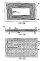
- FIGS. 10A-10D are a schematic illustration of the top view, side view and bottom view of a preferred embodiment of a tamper indicating RFID label of the general type illustrated in FIG. 9 ;
- FIGS. 11A-11C are a schematic illustration of a variation of the RFID label designs of FIGS. 9 and 10 ;
- FIGS. 12A-12E are a schematic illustration of loop tag based on the tamper indicating label designs of FIGS. 9 , 10 and 11 ;
- FIGS. 13A-13C are a schematic illustration of the use of a loop tag of the type illustrated in FIG. 12 ;
- FIG. 14 is a schematic illustration of an object with an integrated electrically conducting path and having a tamper indicating RFID label applied to the object so as to connect to the conducting path on the object and thereby provide an integrated tamper indicating function for the object.
- passive refers to an RFID label or transponder which does not include an on-board power source such as a battery.
- active refers to an RFID label or transponder which includes an on-board power source such as a battery.
- label and tag may be used interchangeably in this document. Where the term label is used, the term tag may validly be substituted. The essential difference between the two are the thicknesses and types of material used in the construction. In general a label will be made from thin, flexible materials, while a tag will be made from thicker, stiffer materials. A tag may, for example, be similar to a plastic card with a pressure sensitive adhesive on the underside. Such tags may be used, for example, as compliance plates or rating plates or specification plates on various types of equipment. A tag, because of its greater thickness, is better suited to active RFID technology.
- a tamper indicating RFID label may include RFID components and one or more tamper indicating electrically conducting paths, known herein as tamper tracks, coupled to the RFID components.
- Each tamper track should be constructed from a destructible conducting path.
- a tamper track can be formed such that it is damaged when the label is tampered.
- relative adhesion characteristics of the tamper track are adapted to break the tamper track when the label is tampered, for example, by removal of the RFID label from an object to which it has been applied.
- the relative adhesion characteristics of the tamper track may be modified by the inclusion of an adhesion modifying layer adjacent to the tamper track.
- the RFD components may retain their RFID capability and detect when the tamper track has been damaged to indicate that the label has been tampered.
- the RFID capability of the RFID components may be disabled when the tamper track is damaged, thereby indicating tampering.
- FIG. 1 is a schematic illustration of the general design of a tamper indicating RFID label according to an embodiment of the invention.
- FIG. 1 shows schematically a pressure sensitive (i.e. self-adhesive) label 100 in cross sectional view.
- the label 100 may include four functionally distinct layers.
- the RFID layer 101 may be a layer which includes RFID components, for example, an RFID memory chip.
- the label 100 may in some embodiments provide an “active” RFID capability, in which case the layer 101 can also include a battery or other power source.
- the second layer 102 may include one or more thin electrically conducting paths which should be coupled to the RFID components in the layer 101 .
- the electrically conducting paths are known herein as “tamper tracks” since they provide a means to detect tampering with or removal of the label 100 from a surface to which it has been applied.
- the layer 101 and the tamper tracks 102 may together provide an RFID capability.
- the layer 101 can provide an RFID capability in its own right, while the tamper tracks 102 can modify the RFID performance of the layer 101 depending on whether said tamper tracks 102 are damaged or not.
- the RFID capability provided by the layer 101 usually includes the ability to store information in the RFID memory chip in the layer 101 , and the ability to read and modify said stored information from a distance. Additional capabilities, such as the ability to encrypt stored information or control access to the stored information, may also be provided.
- the third layer 103 may be an adhesive layer, which in some embodiments is a pressure sensitive adhesive.
- the fourth layer 104 is a top-coat layer applied over the top of the RFID layer 101 .
- the top-coat may be applied to protect the RFID layer and to provide a top surface to accept a printing process.
- the top coat layer 104 is not essential and in some embodiments may not be included.
- the finished construction is the adhesive label 100 .
- the tamper tracks 102 should be destructible.
- the pressure sensitive adhesive 103 damages the tamper tracks 102 —for example, by tearing all or part of them from the underside of the layer 101 —which in turn affects the RFID performance of the label 100 .
- the tamper tracks 102 are electrically connected to the RFID components in the label 100 , and may form part of the RFID components of the label 100 , the RFID function of the label 100 is modified if the label is applied to a surface and subsequently tampered or removed. In this way tampering with or removal of the label 100 can be detected at a distance via the change in the RFID characteristics and response of the label 100 .
- stampering and “tampered” as used herein refer to complete or partial removal of a tamper indicating label, such as the label 100 , from a surface to which it has been applied.
- destructible is used in relation to the tamper tracks 102 in FIG. 1 and in relation to other tamper tracks throughout the document.
- destructible means that the tamper tracks are designed to be damaged or broken in regions of the label which are tampered.
- the tamper tracks 102 may be produced in one of a number of different ways.
- the tamper tracks may be produced by printing electrically conducting ink (such as a carbon/graphite based conductive ink or a precious metal ink).
- the tamper tracks 102 may be produced using electrically conductive adhesive.
- the tamper tracks may be metallic tracks made of Aluminum, Copper or some other suitable metal.
- the tamper tracks 102 should be made from a material, such as an electrically conducting ink, which has appropriate electrical properties but which does not have high intrinsic physical strength. In this way the tamper tracks 102 can be more easily disrupted or damaged as the label 100 is partially or completely removed from a surface to which it has been applied.
- the destructibility of the tamper tracks 102 may be enhanced by including a thin layer 105 of a suitable adhesion modifying coating on the underside of the layer 101 either between the layer 101 and the tamper tracks 102 , or between the tamper tracks 102 and the adhesive layer 103 .
- a suitable adhesion modifying coating may be applied as a uniform layer, or in a specified pattern, or in some other manner such that the properties of the adhesion modifying coating vary across the layer 101 .
- multiple layers of adhesion modifying coating may be applied to “fine tune” the properties of the final composite adhesion modifying coating.
- the adhesion modifying layer 105 is shown between the RFID layer 101 and the tamper tracks 102 , but it should be appreciated that in FIG. 1 and in later figures the adhesion modifying layer 105 may be either between the RFID layer 101 and the tamper tracks 102 or between the tamper tracks 102 and the adhesive layer 103 .
- a adhesion modifying coating 105 between the RFID layer 101 and the tamper tracks 102 results in the adhesion of the layers 101 and 102 to each other being greater or less in a particular region according to whether the adhesion modifying coating 105 is present or absent in that region.
- inclusion of an adhesion modifying coating 105 between the tamper tracks 102 and the adhesive layer 103 results in the adhesion of the layers 102 and 103 to each other being greater or less in a particular region according to whether the adhesion modifying coating 105 is absent or present in that region.
- the adhesion modifying coating 105 reduces the adhesion of two layers that it separates, so that the two layers can be more easily separated.
- the relative adhesion between the layer 101 , adhesion modifying coating 105 , the tamper tracks 102 , and adhesive layer 103 can be adjusted so that when the label 100 is applied to a surface and subsequently tampered or removed, the tamper tracks 102 are damaged. Such damage may preferably occur in a pattern corresponding to the pattern of the adhesion modifying coating 105 . In some embodiments the tamper tracks 102 may be physically separated in a pattern corresponding to the pattern of the adhesion modifying coating 105 , with some of the tamper tracks 102 remaining on the layer 101 and the remainder of the tamper tracks 102 remaining on the adhesive layer 103 . This damage to the tamper tracks 102 may affect the RFID performance of the label 100 .
- the adhesion modifying coating 105 may be a layer of lacquer, or a layer of tamper indicating varnish (for example, similar to that used in some visual tamper indicating label constructions), or a layer of some other suitable material formulation.
- FIG. 2 shows the label 100 in cross section view before and after partial removal from a surface 201 .
- FIG. 2 illustrates in particular the physical disruption of the tamper tracks 102 during tampering or removal of the label 100 .
- FIG. 2 ( a ) the label 100 is shown before removal from the surface 201 .
- the tamper tracks 102 are intact and the label 100 exhibits its normal RFID operation.
- an adhesion modifying layer 105 is applied as a thin layer in a specified pattern between the layer 101 and the tamper tracks 102 .
- the adhesion modifying layer 105 reduces adhesion between the layer 101 and the tamper tracks 102 in those regions where the adhesion modifying layer 105 is applied.
- FIG. 2 ( b ) the label 100 has been partially removed from the surface 201 . As the label 100 is removed, portions of the tamper tracks 102 where there is no adhesion modifying layer 105 remain with the top layer 101 , and complementary portions of the tamper tracks 102 where the adhesion modifying layer 105 has been applied remain with the adhesive layer 103 .
- the differential separation of the tamper tracks 102 is therefore enhanced or achieved through the inclusion of an adhesion modifying coating 105 (as described above) in a specified pattern at the interface between the layer 101 and the tamper tracks 102 , such that the tamper tracks 102 bond less strongly to the layer 101 where the adhesion modifying coating 105 has been applied and therefore in such regions the tamper tracks 102 remain with the adhesive layer 103 when the label 100 is removed from the surface 201 .
- the adhesion modifying layer 105 may be applied in different specified patterns to the layer 101 , or may be applied as a uniform layer to the layer 101 .
- the tamper tracks 102 are damaged, and their electrical properties are thereby affected. This in turn affects the RFID properties of the label 100 , since the tamper tracks 102 are electrically connected to the RFID layer 101 which includes RFID components.
- FIG. 2 the separation of (i.e. damage to) the tamper tracks 102 during tampering of the label 100 is shown to form a regular repeating pattern. It should be appreciated that the pattern of the separation may instead be irregular and may be on a larger or smaller scale relative to the size of the label 100 or the RFID components in the label 100 than shown in FIG. 2 .
- the label 100 may also contain information in another format, such as a barcode, 2D barcode, or some other optical information storage format printed on the top surface of the top coat layer 104 .
- FIG. 3 shows an embodiment of the RFID label 100 in cross sectional view and looking from below through the adhesive layer 103 at the tamper tracks 102 and adhesive modifying layer 105 .
- the adhesion modifying layer 105 is printed in a specified pattern rather than as a solid, continuous layer.
- the RFID layer 101 has two “through-connect” electrical connection points, 301 and 302 , where the electrical circuitry in the RFID layer 101 is connected to the underside of the layer 101 .
- the electrical connection between the points 301 and 302 by means of the tamper track 102 should be intact in order to maintain normal RFID operation of the label 100 .
- the tamper track 102 may be disrupted even if only a portion of the label 100 is tampered.
- the tamper track 102 runs around the perimeter of the underside of the layer 101 between points 301 and 302 .
- This configuration for the tamper track 102 of FIG. 3 ensures that tampering of even a small portion of the label 100 will result in a break in the tamper track 102 and therefore a break in the electrical connection between the points 301 and 302 , which in turn modifies the RFID behavior of the label 100 .
- the tamper track 102 may form all or part of an antenna, in which case the points 301 and 302 may not be electrically connected to each other via a single tamper track 102 .
- An RFID label will generally include an electronic integrated circuit (chip) connected to either an induction loop or an antenna.
- the induction loop or antenna may enable communication and data exchange with a remote RFID reading device. (It should be appreciated that different types of antenna design may be employed.)
- Other electrical or electronic components may also be included in an RFID label.
- An active RFID label will include an onboard power source such as a battery.
- the tamper tracks 102 may be configured on the underside of the RFID layer 101 and coupled to the RFID layer 101. It should be appreciated that in some embodiments the tamper tracks 102 may be designed to be destructible in some regions and durable in other regions. For example, the tamper tracks 102 may include some sections which are durable and rugged, joined by sections which are destructible.
- the tamper tracks 102 may be connected in one of several different ways to the RFID layer 101 , depending on the design and operation of the RFID layer 101 . Several non-limiting examples are listed below.
- the tamper tracks 102 may be connected in series with an induction loop or antenna in the layer 101 .
- the tamper tracks 102 may constitute all or part of the induction loop or antenna of the label 100 .
- the tamper tracks 102 may be part of a tamper-sensing electrical circuit in the label 100 which is separate from the induction loop or antenna of the label 100 .
- FIGS. 4 to 7 are schematic illustrations of further preferred embodiments of the tamper indicating RFID label 100 , showing both a cross sectional view and a view looking from below through the adhesive layer 103 at the tamper tracks 102 and adhesion modifying layer 105 .
- FIGS. 4A , 4 B are a schematic illustration of a preferred embodiment in which the tamper track 102 connects the points 301 and 302 and is in series with an induction loop 401 in the RFID layer 101 .
- the RFID layer 101 may include the induction loop 401 and other components 402 , which may be passive or active.
- the components 402 in one embodiment may be a capacitor which, with the induction loop 401 , forms a resonant electrical circuit.
- the components 402 may include a passive RFID electronic memory chip for storing data.
- the tamper track 102 should be intact for the RFID label 100 of FIG. 4 to be operational.
- the tamper track 102 is broken and the RFID function of the label 100 can be disabled or modified. In this way it can be determined whether or not the label 100 has been tampered.
- An adhesion modifying layer 105 may be included, as described above, to enhance destructibility of the tamper tracks 102 .
- FIGS. 5A , 5 B are a schematic illustration of another preferred embodiment in which the tamper track 102 forms an induction loop 501 for the RFID label 100 .
- the through-connect points 301 and 302 are connected to the RFID components 402 in the layer 110 .
- the tamper track 102 forms a number of loops, with the overall layout of the tamper track 102 acting as an induction loop. Tampering or removing the label 100 results in a break in the tamper track 102 , thereby disabling or modifying the RFID function of the label 100 . In this way it can be determined whether or not the label 100 has been tampered.
- An adhesion modifying coating 105 may be included, as described above, to enhance destructibility of the tamper tracks 102 .
- FIGS. 6A , 6 B are a schematic illustration of another preferred embodiment, which is a variation on the embodiment of FIG. 5 .
- the tamper tracks 102 form an antenna
- the tamper track 102 forms an induction loop.
- the principal difference is that in FIG. 6 the points 301 and 302 are not connected together by a single tamper track 102 . Instead there are two tamper tracks 102 , one starting at point 301 and the other starting at the point 302 .
- the two tamper tracks 102 form an antenna.
- a so-called meander antenna is illustrated, although it should be appreciated that other forms of antenna may also be employed.
- the points 301 and 302 may be connected to each other by the tamper track 102 .
- the through-connect points 301 and 302 are connected to the RFID components 402 in the RFID layer 101 .
- Tampering of the label 100 should result in damage to at least one of the tamper tracks 102 , thereby affecting the characteristics of the antenna and modifying or disabling the RFD function of the label 100 . In this way it can be determined whether or not the label 100 has been tampered.
- An adhesion modifying coating 105 may be included, as described above, to enhance destructibility of the tamper tracks 102 .
- FIGS. 7A-7D are a schematic illustration of another preferred embodiment, based on the embodiments of FIG. 6 .
- the principal difference between the design illustrated in FIG. 6 and the design illustrated in FIG. 7 is that in the design of FIG. 7 the RFID components 402 are on the underside of the layer 101 .
- the RFID components 402 may comprise only an RFID memory chip, in which case in the design of FIG. 7 both the RFID memory chip 402 and the tamper tracks 102 are on the underside of the RFID layer 01 .
- the tamper tracks 102 are designed to be destructible, as described herein.
- An advantage of the design of FIG. 7 compared with the design of FIG. 6 is that in the design of FIG.
- the tamper tracks 102 form an antenna, as in the design of FIG. 6 .
- the tamper tracks 102 may form an induction loop, as in the design of FIG. 5 .
- An adhesion modifying coating 105 may be included, as described above, to enhance destructibility of the tamper tracks 102 .
- the label 100 may be designed to show visual evidence of tampering if the label is tampered with or removed from a surface to which it has been applied.
- Visual tamper indication can be achieved in one of several ways.
- a thin colored layer 701 is applied to the underside of the RFID layer 101 .
- a pattern of visual adhesion-modifying layer may be applied to the underside of the colored layer.
- the visual adhesion-modifying layer may be the same layer or a layer in addition to the RFID adhesion modifying layer 105 described above.
- the presence of the visual adhesion-modifying layer modifies the adhesion of the colored layer 701 to the adhesive layer 103 such that when the label 100 is removed from a surface to which it has been applied, the colored layer 701 breaks up according to the pattern of visual adhesion modifying layer. Areas of color may adhere to the adhesive layer 103 and other complementary areas of color may adhere to the RFID layer 101 .
- An alternative to this embodiment is to apply a pattern of said visual adhesion modifying layer directly to the underside of the RFID layer 101 and apply said thin colored layer to the underside of said visual adhesion modifying layer either before or after application of the tamper tracks 102 .
- the visual adhesion modifying layer may be applied directly to the underside of the RFID layer 101 and a colored adhesive can be used as the adhesive layer 103 .
- a colored adhesive can be used as the adhesive layer 103 .
- the colored adhesive 103 should break up and areas of the colored adhesive may adhere to the RFID layer 101 and complementary areas of the colored adhesive 103 may adhere to the surface. It should be appreciated that other methods may be used to produce a visual tamper indicating effect.
- a portion of the RFID layer 101 and top coat 104 should be transparent so the visual effect can be seen by looking through the RFID layer 101 and top coat 104 . This enables easy inspection of the visual tamper indicating feature without having to remove the label 100 .
- the RFID components in the RFID layer 101 such as an RFID memory chip, may not be transparent, but should only occupy a small portion of the surface area.
- a bar code or serial number may be printed on the top surface of the RFID layer 101 or on the top surface of the top coat 104 (if a top coat 104 is present). Enough of the RFID layer 101 and top coat 104 should be transparent to allow the visual tamper indicating feature to be visible.
- FIGS. 8A , 8 B show illustrations of an RFID label construction and method of manufacture in cross sectional view.
- FIG. 8 illustrates a passive RFID label construction, in which the RFD components 402 consists of an RFID electronic memory chip.
- a pattern 801 of adhesion modifying coating may be applied to the underside of a substrate layer 802 , which may in one embodiment be a polyester layer.
- the tamper tracks 803 can be printed on the underside of the adhesion modifying layer 801 . If necessary the tamper tracks can include a “cross-over”, where a tamper track 803 crosses over itself along a bridging layer of electrical insulator.
- the tamper tracks 803 may be configured to form either an induction loop or antenna of appropriate design and characteristics.
- An RFID electronic memory chip 804 can then be mounted on the underside of the layer 802 and positioned to connect to appropriate terminating points on the tamper tracks 803 .
- the RFID chip 804 and tamper tracks 803 should form an RFID transponder.
- the construction 805 consisting of substrate 802 , adhesion modifying coating 801 , tamper tracks 803 and RFD chip 804 is cut into individual transponders 806 .
- Each transponder 806 is placed in a specified position on the underside of a top coat layer 807 and may be fixed in position with a thin adhesive layer.
- a layer of pressure sensitive adhesive 808 may be applied to the underside of the top coat 807 and individual transponders 806 .
- the resulting construction consisting of top coat layer 807 , individual transponders 806 and adhesive layer 808 is mounted on a suitable carrier film 809 and produced in roll form.
- the resulting roll is die cut into individual labels 810 mounted on the continuous carrier film 809 , where each label 810 includes one transponder 806 .
- the tamper tracks 803 may be produced using an electrically conducting adhesive instead of an electrically conducting ink.
- FIGS. 9A , 9 B are a schematic illustration of another preferred embodiment in which the tamper track 102 forms part of a separate tamper indicating electrical circuit.
- the RFD layer 101 may contain an induction loop or antenna 901 and other electronic components 402 , including an RFID electronic memory chip, to provide an RFID capability.
- the RFID layer 101 should be capable of interacting with an RFID reading device to allow reading of or modification to data stored in the electronic memory chip.
- the through-connect points 301 and 302 are connected to the components 402 in the layer 101 , and to each other via the tamper track 102 .
- the components 402 should be configured to respond differently to a signal from an RFID reader depending on whether or not the points 301 and 302 are connected to each other via the tamper track 102 . If the tamper track 102 is intact, the label 100 will respond in a specified manner to an RFID reader. On the other hand, if the label 100 is tampered, so that the tamper track 102 is damaged and the points 301 and 302 are no longer connected to each other via the tamper track 102 , the label 100 should still respond to an RFID reader but in a different manner, thereby indicating that the label 100 has been tampered. In this way the label 100 of FIG.
- the components 402 may consist only of a passive RFID electronic memory chip, and the tamper track 102 forms a connection, which may be separate from the induction loop or antenna 901 , between two contact points on the RFID memory chip.
- An adhesion modifying coating 105 may be included, as described above, to enhance destructibility of the tamper tracks 102 .
- the components 402 may undergo an irreversible change if the label 100 is tampered and the tamper track 102 is damaged, so that even if the tamper track 102 is subsequently restored, the label 100 will still respond to an RFID reader with a signal indicating it has been tampered.
- the RFID components 402 are “active” (i.e. powered) and are configured to test the integrity of the tamper track 102 either continuously or at specified intervals. In this embodiment if the RFID components 402 detect that the tamper track 102 has been disrupted they may then preferably be configured to record data to this effect in an electronic memory within the components 402 , preferably in a manner which is permanent and irreversible.
- the components 402 may also include a clock.
- the date and time of any tampering of the tamper track 102 or label 100 may also preferably be recorded permanently and irreversibly in an electronic memory within the RFID components 402 .
- FIG. 9 A preferred embodiment of the tamper indicating RFID label configuration of FIG. 9 will now be described by way of non-limiting example with reference to the schematic illustrations shown in FIGS. 10 and 11 .
- antenna may refer to a conventional antenna or to an induction loop (which is used as an antenna at some RFID operating frequencies).
- FIGS. 10A-10D is a schematic illustration of a tamper indicating RFID label 1000 shown in top view, cross sectional side view, and bottom view.
- the label 1000 may include a substrate layer 1001 made of, for example, polyester or some other suitable material. On top of the substrate layer 1001 , electronics to form an RFD transponder, which provides an RFID function, may be applied.
- the electronics may include an RFID electronic memory chip 1002 and an antenna 1003 . (In FIG. 10 an antenna 1003 in the form of an induction loop is shown.)
- FIG. 10D is a more detailed schematic illustration of an example of the electrical connections to the RFID electronic chip 1002 .
- the chip 1002 and antenna 1003 should provide an RFID capability, which may include the ability to store information in the chip 1002 , the ability to read information from the chip 1002 at a distance using a suitable RFID device, and the ability to modify information in the chip 1002 from a distance using a suitable RFD device.
- the chip 1002 may include two contact points, or contact pads, connected to the antenna 1003 , as illustrated in FIGS. 10A and 10D .
- Two contact pads on the chip 1002 can be connected via electrical “through-connects” 1004 to the underside of the substrate layer 1001 .
- One or both or neither of these two contact pads may be the same as the contact pads used to connect the chip 1002 to the antenna 1003 .
- FIG. 10 shows the through-connects 1004 directly beneath the chip 1002 . It should be appreciated that other configurations may instead be used for the through-connects 1004 . In another preferred embodiment, the through-connects 1004 are positioned away from the chip 1002 , and electrical tracks on the top surface of the substrate layer 1001 connect the contact pads on the chip 1002 to the tops of the through-connects 1004 .
- the two through-connect points 1004 on the underside of the substrate layer 1001 are connected to each other by means of a tamper track 1005 which is positioned on the underside of the substrate layer 1001 .
- a layer of adhesive 1006 may also be applied to the underside of the substrate layer 1001 and tamper track 1005 .
- said adhesive 1006 is a pressure sensitive adhesive.
- One or more adhesion modifying layers 1008 may also be provided on the underside of the substrate layer 1001 , as described herein, to promote damage to the tamper track 1005 if the label 1000 is tampered or removed from a surface to which it has been applied.
- a top layer 1007 maybe applied over the top of the substrate 1001 , chip 1002 and antenna 1003 .
- the top layer 1007 can provide protection for these components and can also provide a surface to accept printing—for example printing of a number, a barcode, a logo, or other image.
- the top view is a view looking through the top layer 1007
- the side view is a cross sectional side view
- the bottom view is a view looking though the adhesive layer 1006 at the tamper track 1005 and adhesion modifying layer 1008 .
- the tamper track 1005 is preferably applied to the underside of the substrate layer 1001 , along with one or more layers of adhesion modifying coating 1008 to enhance the destructibility of the tamper track 1005 . Consequently, if the label 1000 is applied to a surface and subsequently tampered or removed, the tamper track 1005 should be broken or disrupted so as to interrupt the electrical connection between the through-connect points 1004 on the underside of the substrate layer 1001 .
- the tamper track 1005 may be laid out in a number of different ways on the underside of the substrate layer 1001 .
- the tamper track runs from one through-connect point 1004 almost all the way around the perimeter of the underside of the substrate layer 1001 and then back to the other through-connect point 1004 , with the outward and return paths of the tamper track 1005 very close together in order to avoid any electrical induction effects which may interfere with the antenna 1003 positioned above on the upper surface of the substrate layer 1001 .
- the width and thickness of the tamper track 1005 can be adjusted to provide the correct properties in terms of electrical resistance and physical destructibility.
- the path made by the tamper track 1005 may run inside, or outside, or directly beneath the antenna 1003 , which in FIG. 10 is an induction loop.
- the tamper track 1005 forms a path which is outside the outer perimeter of the induction loop 1003 , thereby ensuring that any disturbance around the perimeter of the label 1000 will cause the tamper track 1005 to be disrupted.
- the tamper track 1005 When the label 1000 is applied to a surface, the tamper track 1005 is intact and the corresponding contact pads on the chip 1002 are electrically connected to each other. When the label 1000 is removed or substantially tampered with, the tamper track 1005 should be broken or disrupted and there will then be an open circuit between the corresponding contact pads on the chip 1002 . When such an open circuit occurs, the response of the RFD chip 1002 or the information stored in the chip 1002 will be modified in a way which can be detected by an RFID reader.
- the modified chip response or modified chip information can be detected during the first read operation of the label after the label 1000 is removed or tampered, and the reader (if it has a write capability) can be programmed to write data back to the chip 1002 to indicate that the label 1000 has been removed or tampered.
- Said data which is written back to the chip 1002 to indicate removal or tampering of the label 1000 is preferably permanent and irreversible, to prevent the memory contents of the chip being altered back to the original state to disguise the fact that the label has been moved or tampered.
- an RFD read/write device capable of detecting the change in RFD performance of the label 1000 when the label 1000 is tampered, and writing data back to the chip 1002 within the label 1000 to indicate such tampering has occurred, said data preferably being written into the chip 1002 so as to be permanent and irreversible.
- the label 1000 can be configured such that any disruption to the tamper track 1005 can be detected internally within the label 1000 without requiring an RFID read operation.
- the chip 1002 can be programmed to modify its own memory contents to indicate that the label 1000 has been removed or tampered. Said modification to the memory contents of the chip 1002 to indicate removal or tampering of the label 1000 should preferably be permanent and irreversible, to prevent the memory contents of the chip being altered back to the original state to disguise the fact that the label has been moved or tampered.
- the label 1000 may function as a normal RFID label when it is first applied to a surface. After is the label is moved or tampered, the RFID function of the label 1000 may be maintained and information can be read from and written to the RFD chip 1002 , while the label 1000 also provides an RFID means to determine that it has been moved or tampered.
- FIGS. 11A-11C are a variation on the preferred embodiment of FIGS. 9 and 10 .
- the basic design of the label 1000 in FIG. 11 is similar to that of FIG. 10 .
- the difference in the design of FIG. 11 is that the tamper track 1005 extends well beyond the antenna 1003 or other RFID components in at least one direction.
- the tamper track 1005 should preferably run around the perimeter of the label 1000 and detect tampering of any edge portion of the label, whether near the chip 1002 and antenna 1003 or at the end of the label away from these components.
- the label 1000 can, for example, be applied around a corner so that the chip 1002 and antenna 1003 are on a flat surface while the other end of the label 1000 , which includes the tamper track 1005 , extends around said corner.
- One or more adhesion modifying layers 1008 may also be provided on the underside of the substrate layer 1001 , as described herein, to promote damage to the tamper track 1005 if the label 1000 is tampered or removed from a surface to which it has been applied.
- FIGS. 12A-12E are another variation on the embodiment of FIGS. 10 and 11 .
- FIG. 12 is a schematic illustration of a tamper indicating RFID loop tag 1200 , shown in top view, side view and bottom view.
- the tamper track 1005 on the underside of the substrate 1001 extends beyond the antenna 1003 and forms a “tail” 1201 .
- the tamper track 1005 is straight and connects the two through-connect points 1004 .
- the substrate 1001 may be cut approximately to the shape of the electronics, so that the loop tag 1200 is broad at the end which includes the antenna 1003 and narrow at the tail 1201 .
- the loop tag may be cut into any other shape around the electronic components.
- the tamper track 1005 will extend to the end of the tail 1201 .
- a bottom layer 1202 may also be applied to a specific portion of the underside of the substrate 1001 and tamper track 1005 .
- the tamper track should extend into the region 1203 of the underside of the substrate 1001 which is not covered with the bottom layer 1202 .
- an adhesive such as a pressure sensitive adhesive 1204 may be applied to the underside of the substrate 1001 and the tamper track 1005 .
- an adhesion modifying layer may also be included in the region 1203 .
- a top layer 1007 may be applied over the top of the substrate 1001 , chip 1002 and antenna 1003 .
- the top layer 1007 may provide protection for these components and may also provide a surface to accept printing—for example printing of a number, a barcode, a logo, or other image.
- top view is a view looking through the top layer 1007 to the chip 1002 and antenna 1003
- bottom view is a view looking through the bottom layer 1202 and adhesive 1204 to the tamper track 1005 and through-connects 1004 .
- the loop tag 1200 may be bent into a loop 1205 ( FIG. 12D ) and the region 1203 of pressure sensitive adhesive can be pressed against a region of the bottom layer 1202 , as shown.
- the pressure sensitive adhesive 1204 should hold the loop 1205 closed.
- a loop 1206 FIG. 12E may be formed by pressing the region 1203 of pressure sensitive adhesive 1204 against a region of the top layer 1007 , as also shown.
- loops 1205 and 1206 do not show the internal components—such as the chip 1002 , antenna 1003 and tamper track 1005 —or the separate layers of the loop tag construction.
- the two regions of the loop tag which are joined together in this way by the pressure sensitive adhesive 1204 preferably both include electronics—for example, the chip 1002 , or the antenna 1003 , or the tamper track 1005 —in order to ensure the closed loop cannot be cut and the loop opened without the RFD performance of the loop tag 1200 being affected.
- the tamper track tail 1201 may be looped back and fixed to another portion of the tamper track tail 1201 or may be looped back and fixed to a region of the underside of the antenna 1003 (as illustrated in the loop 1205 ).
- the substrate 1001 , pressure sensitive adhesive 1204 , tamper track 1005 , and any adhesion modifying coatings which are applied are preferably designed as described herein such that the tamper track 1005 is damaged when the closed loop is pulled apart in the region of pressure sensitive adhesive 1204 , thereby modifying the RFID performance of the loop tag 1200 , as described above in relation to the label constructions of FIGS. 9 and 10 .
- a similar modification to the performance of the loop tag 1200 will occur if the closed loop 1205 or 1206 is cut in order to open the loop.
- FIGS. 13A-13C are a schematic illustration of the use of the loop tag 1200 to detect opening of a container 1300 which includes a body 1301 and lid 1302 .
- the body 1301 and lid 1302 have holes 1303 which align when the lid 1302 is placed properly on the body 1301 of the container 1300 .
- FIG. 13 shows a cutaway cross sectional view ( FIG. 13B ) of a portion of the body 1301 and lid 1302 of the container 1300 in the region of the holes 1303 .
- the loop tag 1200 is applied to the container 1300 with the open loop portion 1304 passing through the aligned holes 1303 .
- the RFID chip 1002 in the loop tag 1200 may store information about the contents of the container 1300 . If the loop tag 1200 is removed from the container 1300 , either by pulling the loop 1304 apart to open the loop or by cutting the loop tag 1200 , the tamper track 1005 will be interrupted and the RFID performance of the loop tag 1200 will be modified in a manner detectable by an RFID reader, as described above in relation to the label construction of FIGS. 9 , 10 , 11 and 12 .
- loop tag 1200 does not need to have a narrow tail region.
- the loop tag may instead be rectangular in shape, as illustrated schematically in the embodiment of FIG. 11 .
- a tamper indicating label is incorporated with an object to which the label is to be applied.
- the label used maybe any of the embodiments described above.
- FIG. 14 illustrates a label 1401 applied to an object 1402 .
- a conductive path 1403 should be incorporated into the object 1402 .
- a conducting path of electrically conducting ink may be formed around the object 1402 .
- the conducting path 1403 on the object 1402 should have at least two end points.
- the tamper tracks in the label 1401 should have a corresponding number of connection points. When the label 1401 is applied to the object 1402 , each end point should be connected to a connection point.
- the conducting path on the object 1402 and the tamper tracks in the label 1401 should together form one or more circuits, each from a tamper track to an endpoint, through the conducting path on the object 1402 , to the other end point and back to a tamper track. If a tamper track is disrupted through the label 1401 being tampered, or if connection between a tamper track and the conducting path on the object 1402 is broken, the RFID function of the label 1401 may be modified in a manner as described above to indicate tampering. For example, if the label 1401 is applied to a cardboard box and the entire label and that part of the box that the label is adhered to is cut out, tampering is indicated.
Abstract
A tamper indicating label is provided. The label may include RFID components and a tamper track coupled to the RFID components. The tamper track should be constructed from a destructible conducting path. Additionally, the tamper track can be formed such that it is damaged when the label is tampered. In one embodiment, adhesion characteristics of the tamper track are adapted to break apart the tamper track when the label is tampered, for example, by removal from an object. The RFID components may retain their RF capability and detect when the tamper track has been damaged to indicate that the label has been tampered. Alternatively, the RFID capability of the RFID components may be disabled when the tamper track is damaged, indicating tampering.
Description
This application claims the benefit of Provisional application Ser. No. 60/190,936, filed Mar. 21, 2000.
Radio Frequency Identification (RFID) is being used increasingly as a means to identify goods at a distance, without requiring physical contact or even line of sight access to the goods. RFID enables information about an item to be stored on an item, and in some implementations also allows this stored information to be modified at a distance. The most compact and cost effective means to provide this RFID capability is by means of a pressure sensitive (i.e. self adhesive) label incorporating an RFID capability.
The ability to detect remotely whether a pressure sensitive label or seal applied to an item has been tampered with or removed is becoming increasingly important in order to detect theft, product substitution, tampering, warranty violation and other problems.
A disadvantage of current pressure sensitive RFID label technology is that it does not allow the remote determination of whether or not a label has been tampered with or removed and relocated.
A tamper indicating label is provided. The label may comprise RFID components and a tamper track connected to the RFID components. The tamper track is preferably formed by destructible electronics. The tamper track may be modified when the label is tampered with. In one embodiment, the RFID components are able to detect the modification in the tamper track while maintaining their RFID capability. Detection of the modification in the tamper track indicates tampering with the label. In an alternative embodiment, the modification in the tamper track disables the RFID function.
In a further embodiment, the label comprises an RFID layer. The RFID layer may include a memory chip and at least one of an antenna or loop inductor. Means for attaching the RFID layer to an object may also be provided. The means for attaching may be an adhesive layer. The adhesive layer can support the RFID layer. A destructible conducting path may be sandwiched between the RFID layer and the adhesive layer. The destructible conducting path should be disrupted when the label is tampered. The disruption preferably modifies in some way the RFID characteristics of the RFID layer.
In a further embodiment, at least a part of the destructible conducting path may in contact with the adhesive layer. The destructible conducting path can thereby be modified when the label is at least partially removed from a surface, and in turn, modify RFID characteristics of the label, indicating tampering.
According to another embodiment, the invention includes an RFID system. A substrate having a top and a bottom surface is provided. RFID electronic components are applied to the bottom surface of the substrate. A conductive layer may also be formed in a pattern on the bottom surface of the substrate. An adhesive layer may support the substrate such that the RFID electronic components and the conductive layer are sandwiched between the substrate and the adhesive layer. The adhesive layer, the substrate, and conductive layer should have relative adhesion strengths such that when the system is partially removed from a surface to which it has been applied, at least one of the RFID components and the conductive layer is altered to modify the RFID characteristics of the system.
According to another embodiment of the invention, a security apparatus for indicating tampering is provided. Here, an object may be provided with a conducting path having at least two end points. A security label is arranged on the object. The security label may be a tamper indicating label as described above and should include RFID components and a destructible conducting path between the RF components and each individual end point.
In one of the more detailed embodiments of the invention, a security label is combined with an object. The security label may comprise RFID components and means for attaching the RFID components to the object. Destructible electronics may be connected to the RFID components. The destructible electronics can be broken when the label is at least partially removed from the object. The object comprises a surface for receiving the security label and a conducting path having two ends. The ends of the conducting path may be connected to the destructible electronics thereby forming a circuit through the RFID components, the destructible electronics and the conducting path. The RFID characteristics of the RFID components may be modified if the connection between the end points and the destructible electronics is broken.
According to another embodiment of the invention, a substrate having first and second portions is provided. The second portion of the substrate may be adapted to be looped back and connected to the first portion. An RFID transponder can be arranged on the substrate. A tamper track may be coupled to the RFID transponder and should extend at least partially into the second portion of the substrate. An adhesive layer should be provided on at least a part of the second portion of the substrate that includes the tamper track. The tamper track in that part of the substrate may be adapted to be modified when the label is tampered with due to the relative adhesion strength of the tamper track.
The present invention will now be described by way of non-limiting example with reference to the accompanying drawings, wherein:
The term “passive”, as used herein, refers to an RFID label or transponder which does not include an on-board power source such as a battery. The term “active”, as used herein, refers to an RFID label or transponder which includes an on-board power source such as a battery. The advantages of an active RFID label, relative to a passive RFID label, are that an active RFID label can include continuous on-board functions such as a clock, and can usually enable longer data reading and writing distances. A disadvantage of active RFID labels, relative to passive RFID labels, is that active RFID labels are physically larger due to the need to carry an on-board power source.
It should be appreciated that the terms label and tag may be used interchangeably in this document. Where the term label is used, the term tag may validly be substituted. The essential difference between the two are the thicknesses and types of material used in the construction. In general a label will be made from thin, flexible materials, while a tag will be made from thicker, stiffer materials. A tag may, for example, be similar to a plastic card with a pressure sensitive adhesive on the underside. Such tags may be used, for example, as compliance plates or rating plates or specification plates on various types of equipment. A tag, because of its greater thickness, is better suited to active RFID technology.
It should be appreciated that the illustrations herein are not to scale. In general the thicknesses of the label constructions (and component layers thereof) illustrated in the figures have been exaggerated, to illustrate more clearly the internal structures and components.
In general, a tamper indicating RFID label is provided. The label may include RFID components and one or more tamper indicating electrically conducting paths, known herein as tamper tracks, coupled to the RFID components. Each tamper track should be constructed from a destructible conducting path. Additionally, a tamper track can be formed such that it is damaged when the label is tampered. In one embodiment, relative adhesion characteristics of the tamper track are adapted to break the tamper track when the label is tampered, for example, by removal of the RFID label from an object to which it has been applied. In one embodiment, the relative adhesion characteristics of the tamper track may be modified by the inclusion of an adhesion modifying layer adjacent to the tamper track. The RFD components may retain their RFID capability and detect when the tamper track has been damaged to indicate that the label has been tampered. Alternatively, the RFID capability of the RFID components may be disabled when the tamper track is damaged, thereby indicating tampering.
The RFID layer 101 may be a layer which includes RFID components, for example, an RFID memory chip. The label 100 may in some embodiments provide an “active” RFID capability, in which case the layer 101 can also include a battery or other power source.
The second layer 102 may include one or more thin electrically conducting paths which should be coupled to the RFID components in the layer 101. The electrically conducting paths are known herein as “tamper tracks” since they provide a means to detect tampering with or removal of the label 100 from a surface to which it has been applied.
The layer 101 and the tamper tracks 102 may together provide an RFID capability. On the other hand, in some embodiments the layer 101 can provide an RFID capability in its own right, while the tamper tracks 102 can modify the RFID performance of the layer 101 depending on whether said tamper tracks 102 are damaged or not.
The RFID capability provided by the layer 101, or the layers 101 and 102 together, usually includes the ability to store information in the RFID memory chip in the layer 101, and the ability to read and modify said stored information from a distance. Additional capabilities, such as the ability to encrypt stored information or control access to the stored information, may also be provided.
The third layer 103 may be an adhesive layer, which in some embodiments is a pressure sensitive adhesive.
The fourth layer 104 is a top-coat layer applied over the top of the RFID layer 101. The top-coat may be applied to protect the RFID layer and to provide a top surface to accept a printing process. The top coat layer 104 is not essential and in some embodiments may not be included. The finished construction is the adhesive label 100.
The tamper tracks 102 should be destructible. When the label 100 is applied to a surface and subsequently tampered or removed, the pressure sensitive adhesive 103 damages the tamper tracks 102—for example, by tearing all or part of them from the underside of the layer 101—which in turn affects the RFID performance of the label 100. Since the tamper tracks 102 are electrically connected to the RFID components in the label 100, and may form part of the RFID components of the label 100, the RFID function of the label 100 is modified if the label is applied to a surface and subsequently tampered or removed. In this way tampering with or removal of the label 100 can be detected at a distance via the change in the RFID characteristics and response of the label 100.
The terms “tampering” and “tampered” as used herein refer to complete or partial removal of a tamper indicating label, such as the label 100, from a surface to which it has been applied.
In this document the term “destructible” is used in relation to the tamper tracks 102 in FIG. 1 and in relation to other tamper tracks throughout the document. In this context the term destructible means that the tamper tracks are designed to be damaged or broken in regions of the label which are tampered.
The tamper tracks 102 may be produced in one of a number of different ways. In one preferred embodiment, the tamper tracks may be produced by printing electrically conducting ink (such as a carbon/graphite based conductive ink or a precious metal ink). In another preferred embodiment the tamper tracks 102 may be produced using electrically conductive adhesive. In another embodiment the tamper tracks may be metallic tracks made of Aluminum, Copper or some other suitable metal.
In general the tamper tracks 102 should be made from a material, such as an electrically conducting ink, which has appropriate electrical properties but which does not have high intrinsic physical strength. In this way the tamper tracks 102 can be more easily disrupted or damaged as the label 100 is partially or completely removed from a surface to which it has been applied.
In some preferred embodiments the destructibility of the tamper tracks 102 may be enhanced by including a thin layer 105 of a suitable adhesion modifying coating on the underside of the layer 101 either between the layer 101 and the tamper tracks 102, or between the tamper tracks 102 and the adhesive layer 103. Preferably, at least a part of the tamper tracks should contact the adhesive 103. The layer of adhesion modifying coating may be applied as a uniform layer, or in a specified pattern, or in some other manner such that the properties of the adhesion modifying coating vary across the layer 101. In some embodiments multiple layers of adhesion modifying coating may be applied to “fine tune” the properties of the final composite adhesion modifying coating. In the illustration of FIG. 1 the adhesion modifying layer 105 is shown between the RFID layer 101 and the tamper tracks 102, but it should be appreciated that in FIG. 1 and in later figures the adhesion modifying layer 105 may be either between the RFID layer 101 and the tamper tracks 102 or between the tamper tracks 102 and the adhesive layer 103.
Inclusion of a adhesion modifying coating 105 between the RFID layer 101 and the tamper tracks 102 results in the adhesion of the layers 101 and 102 to each other being greater or less in a particular region according to whether the adhesion modifying coating 105 is present or absent in that region. Similarly, inclusion of an adhesion modifying coating 105 between the tamper tracks 102 and the adhesive layer 103 results in the adhesion of the layers 102 and 103 to each other being greater or less in a particular region according to whether the adhesion modifying coating 105 is absent or present in that region. Usually, but not necessarily, the adhesion modifying coating 105 reduces the adhesion of two layers that it separates, so that the two layers can be more easily separated.
The relative adhesion between the layer 101, adhesion modifying coating 105, the tamper tracks 102, and adhesive layer 103 can be adjusted so that when the label 100 is applied to a surface and subsequently tampered or removed, the tamper tracks 102 are damaged. Such damage may preferably occur in a pattern corresponding to the pattern of the adhesion modifying coating 105. In some embodiments the tamper tracks 102 may be physically separated in a pattern corresponding to the pattern of the adhesion modifying coating 105, with some of the tamper tracks 102 remaining on the layer 101 and the remainder of the tamper tracks 102 remaining on the adhesive layer 103. This damage to the tamper tracks 102 may affect the RFID performance of the label 100.
The adhesion modifying coating 105 may be a layer of lacquer, or a layer of tamper indicating varnish (for example, similar to that used in some visual tamper indicating label constructions), or a layer of some other suitable material formulation.
The tamper indicating characteristics of one preferred embodiment of the label 100 are illustrated in FIG. 2 , which shows the label 100 in cross section view before and after partial removal from a surface 201. FIG. 2 illustrates in particular the physical disruption of the tamper tracks 102 during tampering or removal of the label 100. In FIG. 2(a) the label 100 is shown before removal from the surface 201. Here the tamper tracks 102 are intact and the label 100 exhibits its normal RFID operation. In this preferred embodiment an adhesion modifying layer 105 is applied as a thin layer in a specified pattern between the layer 101 and the tamper tracks 102. In this preferred embodiment the adhesion modifying layer 105 reduces adhesion between the layer 101 and the tamper tracks 102 in those regions where the adhesion modifying layer 105 is applied. In FIG. 2(b) the label 100 has been partially removed from the surface 201. As the label 100 is removed, portions of the tamper tracks 102 where there is no adhesion modifying layer 105 remain with the top layer 101, and complementary portions of the tamper tracks 102 where the adhesion modifying layer 105 has been applied remain with the adhesive layer 103. The differential separation of the tamper tracks 102 is therefore enhanced or achieved through the inclusion of an adhesion modifying coating 105 (as described above) in a specified pattern at the interface between the layer 101 and the tamper tracks 102, such that the tamper tracks 102 bond less strongly to the layer 101 where the adhesion modifying coating 105 has been applied and therefore in such regions the tamper tracks 102 remain with the adhesive layer 103 when the label 100 is removed from the surface 201. In other embodiments the adhesion modifying layer 105 may be applied in different specified patterns to the layer 101, or may be applied as a uniform layer to the layer 101. As the label 100 is removed from the surface 201, the tamper tracks 102 are damaged, and their electrical properties are thereby affected. This in turn affects the RFID properties of the label 100, since the tamper tracks 102 are electrically connected to the RFID layer 101 which includes RFID components. In FIG. 2 the separation of (i.e. damage to) the tamper tracks 102 during tampering of the label 100 is shown to form a regular repeating pattern. It should be appreciated that the pattern of the separation may instead be irregular and may be on a larger or smaller scale relative to the size of the label 100 or the RFID components in the label 100 than shown in FIG. 2.
The label 100 may also contain information in another format, such as a barcode, 2D barcode, or some other optical information storage format printed on the top surface of the top coat layer 104.
A preferred embodiment of the tamper tracks 102 will now be described with reference to FIG. 3 , which shows an embodiment of the RFID label 100 in cross sectional view and looking from below through the adhesive layer 103 at the tamper tracks 102 and adhesive modifying layer 105. In the embodiment of FIG. 3 the adhesion modifying layer 105 is printed in a specified pattern rather than as a solid, continuous layer. In FIG. 3 the RFID layer 101 has two “through-connect” electrical connection points, 301 and 302, where the electrical circuitry in the RFID layer 101 is connected to the underside of the layer 101. In this embodiment the electrical connection between the points 301 and 302 by means of the tamper track 102 should be intact in order to maintain normal RFID operation of the label 100.
Preferably the tamper track 102 may be disrupted even if only a portion of the label 100 is tampered. In FIG. 3 the tamper track 102 runs around the perimeter of the underside of the layer 101 between points 301 and 302. This configuration for the tamper track 102 of FIG. 3 ensures that tampering of even a small portion of the label 100 will result in a break in the tamper track 102 and therefore a break in the electrical connection between the points 301 and 302, which in turn modifies the RFID behavior of the label 100.
It should be appreciated that other configurations of the tamper track 102 could also be employed. For example, in some embodiments the tamper track 102 may form all or part of an antenna, in which case the points 301 and 302 may not be electrically connected to each other via a single tamper track 102.
An RFID label will generally include an electronic integrated circuit (chip) connected to either an induction loop or an antenna. The induction loop or antenna may enable communication and data exchange with a remote RFID reading device. (It should be appreciated that different types of antenna design may be employed.) Other electrical or electronic components may also be included in an RFID label. An active RFID label will include an onboard power source such as a battery.
Preferred embodiments of ways in which the tamper tracks 102 may be configured on the underside of the RFID layer 101 and coupled to the RFID layer 101 will be now be described by way of non-limiting example. It should be appreciated that in some embodiments the tamper tracks 102 may be designed to be destructible in some regions and durable in other regions. For example, the tamper tracks 102 may include some sections which are durable and rugged, joined by sections which are destructible.
The tamper tracks 102 may be connected in one of several different ways to the RFID layer 101, depending on the design and operation of the RFID layer 101. Several non-limiting examples are listed below.
1. The tamper tracks 102 may be connected in series with an induction loop or antenna in the layer 101.
2. The tamper tracks 102 may constitute all or part of the induction loop or antenna of the label 100.
3. The tamper tracks 102 may be part of a tamper-sensing electrical circuit in the label 100 which is separate from the induction loop or antenna of the label 100.
In order to provide an additional indicator of tampering, the label 100 may be designed to show visual evidence of tampering if the label is tampered with or removed from a surface to which it has been applied. Visual tamper indication can be achieved in one of several ways. In one embodiment a thin colored layer 701 is applied to the underside of the RFID layer 101. A pattern of visual adhesion-modifying layer may be applied to the underside of the colored layer. The visual adhesion-modifying layer may be the same layer or a layer in addition to the RFID adhesion modifying layer 105 described above. The presence of the visual adhesion-modifying layer modifies the adhesion of the colored layer 701 to the adhesive layer 103 such that when the label 100 is removed from a surface to which it has been applied, the colored layer 701 breaks up according to the pattern of visual adhesion modifying layer. Areas of color may adhere to the adhesive layer 103 and other complementary areas of color may adhere to the RFID layer 101. An alternative to this embodiment is to apply a pattern of said visual adhesion modifying layer directly to the underside of the RFID layer 101 and apply said thin colored layer to the underside of said visual adhesion modifying layer either before or after application of the tamper tracks 102. In another embodiment, the visual adhesion modifying layer may be applied directly to the underside of the RFID layer 101 and a colored adhesive can be used as the adhesive layer 103. In this case, when the label is removed from a surface to which it has been applied, the colored adhesive 103 should break up and areas of the colored adhesive may adhere to the RFID layer 101 and complementary areas of the colored adhesive 103 may adhere to the surface. It should be appreciated that other methods may be used to produce a visual tamper indicating effect.
When using a visual tamper indicating effect, a portion of the RFID layer 101 and top coat 104 (if a top coat 104 is present) should be transparent so the visual effect can be seen by looking through the RFID layer 101 and top coat 104. This enables easy inspection of the visual tamper indicating feature without having to remove the label 100. The RFID components in the RFID layer 101, such as an RFID memory chip, may not be transparent, but should only occupy a small portion of the surface area.
Additionally, it may be desired to print information or patterns on the label. For example, as described above, a bar code or serial number may be printed on the top surface of the RFID layer 101 or on the top surface of the top coat 104 (if a top coat 104 is present). Enough of the RFID layer 101 and top coat 104 should be transparent to allow the visual tamper indicating feature to be visible.
Method of Manufacture
A preferred method of manufacture for the label configuration described above in relation to FIG. 7 is now described and illustrated schematically in FIGS. 8A , 8B, which show illustrations of an RFID label construction and method of manufacture in cross sectional view.
The diagram of FIG. 8 illustrates a passive RFID label construction, in which the RFD components 402 consists of an RFID electronic memory chip.
A pattern 801 of adhesion modifying coating may be applied to the underside of a substrate layer 802, which may in one embodiment be a polyester layer. The tamper tracks 803 can be printed on the underside of the adhesion modifying layer 801. If necessary the tamper tracks can include a “cross-over”, where a tamper track 803 crosses over itself along a bridging layer of electrical insulator. The tamper tracks 803 may be configured to form either an induction loop or antenna of appropriate design and characteristics. An RFID electronic memory chip 804 can then be mounted on the underside of the layer 802 and positioned to connect to appropriate terminating points on the tamper tracks 803. The RFID chip 804 and tamper tracks 803 should form an RFID transponder. The construction 805 consisting of substrate 802, adhesion modifying coating 801, tamper tracks 803 and RFD chip 804 is cut into individual transponders 806. Each transponder 806 is placed in a specified position on the underside of a top coat layer 807 and may be fixed in position with a thin adhesive layer. A layer of pressure sensitive adhesive 808 may be applied to the underside of the top coat 807 and individual transponders 806. The resulting construction consisting of top coat layer 807, individual transponders 806 and adhesive layer 808 is mounted on a suitable carrier film 809 and produced in roll form. The resulting roll is die cut into individual labels 810 mounted on the continuous carrier film 809, where each label 810 includes one transponder 806.
In a variation on the method of manufacture illustrated in FIG. 8 , the tamper tracks 803 may be produced using an electrically conducting adhesive instead of an electrically conducting ink.
Tamper Indicating RFD Label with Tracking Capability
In a variation on the embodiments described above, the components 402 may undergo an irreversible change if the label 100 is tampered and the tamper track 102 is damaged, so that even if the tamper track 102 is subsequently restored, the label 100 will still respond to an RFID reader with a signal indicating it has been tampered. In one preferred embodiment the RFID components 402 are “active” (i.e. powered) and are configured to test the integrity of the tamper track 102 either continuously or at specified intervals. In this embodiment if the RFID components 402 detect that the tamper track 102 has been disrupted they may then preferably be configured to record data to this effect in an electronic memory within the components 402, preferably in a manner which is permanent and irreversible. Preferably, if the components 402 are active, they may also include a clock. In this case, the date and time of any tampering of the tamper track 102 or label 100 may also preferably be recorded permanently and irreversibly in an electronic memory within the RFID components 402.
A preferred embodiment of the tamper indicating RFID label configuration of FIG. 9 will now be described by way of non-limiting example with reference to the schematic illustrations shown in FIGS. 10 and 11 .
It should be appreciated that the term antenna as used below may refer to a conventional antenna or to an induction loop (which is used as an antenna at some RFID operating frequencies).
The label 1000 may include a substrate layer 1001 made of, for example, polyester or some other suitable material. On top of the substrate layer 1001, electronics to form an RFD transponder, which provides an RFID function, may be applied. The electronics may include an RFID electronic memory chip 1002 and an antenna 1003. (In FIG. 10 an antenna 1003 in the form of an induction loop is shown.)
The chip 1002 and antenna 1003 should provide an RFID capability, which may include the ability to store information in the chip 1002, the ability to read information from the chip 1002 at a distance using a suitable RFID device, and the ability to modify information in the chip 1002 from a distance using a suitable RFD device.
The chip 1002 may include two contact points, or contact pads, connected to the antenna 1003, as illustrated in FIGS. 10A and 10D .
Two contact pads on the chip 1002 can be connected via electrical “through-connects” 1004 to the underside of the substrate layer 1001. One or both or neither of these two contact pads may be the same as the contact pads used to connect the chip 1002 to the antenna 1003.
The two through-connect points 1004 on the underside of the substrate layer 1001 are connected to each other by means of a tamper track 1005 which is positioned on the underside of the substrate layer 1001.
A layer of adhesive 1006 may also be applied to the underside of the substrate layer 1001 and tamper track 1005. Preferably said adhesive 1006 is a pressure sensitive adhesive. One or more adhesion modifying layers 1008 may also be provided on the underside of the substrate layer 1001, as described herein, to promote damage to the tamper track 1005 if the label 1000 is tampered or removed from a surface to which it has been applied.
A top layer 1007 maybe applied over the top of the substrate 1001, chip 1002 and antenna 1003. The top layer 1007 can provide protection for these components and can also provide a surface to accept printing—for example printing of a number, a barcode, a logo, or other image.
It should be appreciated that in FIG. 10 the top view is a view looking through the top layer 1007, the side view is a cross sectional side view, and the bottom view is a view looking though the adhesive layer 1006 at the tamper track 1005 and adhesion modifying layer 1008.
The tamper track 1005 is preferably applied to the underside of the substrate layer 1001, along with one or more layers of adhesion modifying coating 1008 to enhance the destructibility of the tamper track 1005. Consequently, if the label 1000 is applied to a surface and subsequently tampered or removed, the tamper track 1005 should be broken or disrupted so as to interrupt the electrical connection between the through-connect points 1004 on the underside of the substrate layer 1001.
The tamper track 1005 may be laid out in a number of different ways on the underside of the substrate layer 1001. In the preferred embodiment illustrated in FIG. 10 , the tamper track runs from one through-connect point 1004 almost all the way around the perimeter of the underside of the substrate layer 1001 and then back to the other through-connect point 1004, with the outward and return paths of the tamper track 1005 very close together in order to avoid any electrical induction effects which may interfere with the antenna 1003 positioned above on the upper surface of the substrate layer 1001. The width and thickness of the tamper track 1005 can be adjusted to provide the correct properties in terms of electrical resistance and physical destructibility. The path made by the tamper track 1005 may run inside, or outside, or directly beneath the antenna 1003, which in FIG. 10 is an induction loop. In one preferred embodiment the tamper track 1005 forms a path which is outside the outer perimeter of the induction loop 1003, thereby ensuring that any disturbance around the perimeter of the label 1000 will cause the tamper track 1005 to be disrupted.
When the label 1000 is applied to a surface, the tamper track 1005 is intact and the corresponding contact pads on the chip 1002 are electrically connected to each other. When the label 1000 is removed or substantially tampered with, the tamper track 1005 should be broken or disrupted and there will then be an open circuit between the corresponding contact pads on the chip 1002. When such an open circuit occurs, the response of the RFD chip 1002 or the information stored in the chip 1002 will be modified in a way which can be detected by an RFID reader.
If the label 1000 is passive (i.e. without an on-board battery or other power source), the modified chip response or modified chip information can be detected during the first read operation of the label after the label 1000 is removed or tampered, and the reader (if it has a write capability) can be programmed to write data back to the chip 1002 to indicate that the label 1000 has been removed or tampered. Said data which is written back to the chip 1002 to indicate removal or tampering of the label 1000 is preferably permanent and irreversible, to prevent the memory contents of the chip being altered back to the original state to disguise the fact that the label has been moved or tampered. There is therefore disclosed herein an RFD read/write device capable of detecting the change in RFD performance of the label 1000 when the label 1000 is tampered, and writing data back to the chip 1002 within the label 1000 to indicate such tampering has occurred, said data preferably being written into the chip 1002 so as to be permanent and irreversible.
If the label 1000 is active (i.e. has an on-board battery or other power source), it can be configured such that any disruption to the tamper track 1005 can be detected internally within the label 1000 without requiring an RFID read operation. When such disruption to the tamper track 1005 is detected internally, the chip 1002 can be programmed to modify its own memory contents to indicate that the label 1000 has been removed or tampered. Said modification to the memory contents of the chip 1002 to indicate removal or tampering of the label 1000 should preferably be permanent and irreversible, to prevent the memory contents of the chip being altered back to the original state to disguise the fact that the label has been moved or tampered.
Hence the label 1000 may function as a normal RFID label when it is first applied to a surface. After is the label is moved or tampered, the RFID function of the label 1000 may be maintained and information can be read from and written to the RFD chip 1002, while the label 1000 also provides an RFID means to determine that it has been moved or tampered.
In FIG. 12 , the tamper track 1005 on the underside of the substrate 1001 extends beyond the antenna 1003 and forms a “tail” 1201. In the embodiment shown in FIG. 12 , the tamper track 1005 is straight and connects the two through-connect points 1004. The substrate 1001 may be cut approximately to the shape of the electronics, so that the loop tag 1200 is broad at the end which includes the antenna 1003 and narrow at the tail 1201. Alternatively, the loop tag may be cut into any other shape around the electronic components. Preferably, the tamper track 1005 will extend to the end of the tail 1201.
A bottom layer 1202 may also be applied to a specific portion of the underside of the substrate 1001 and tamper track 1005. The tamper track should extend into the region 1203 of the underside of the substrate 1001 which is not covered with the bottom layer 1202. In the region 1203 where the bottom layer 1202 is not applied, an adhesive, such as a pressure sensitive adhesive 1204 may be applied to the underside of the substrate 1001 and the tamper track 1005. As described herein, an adhesion modifying layer may also be included in the region 1203.
A top layer 1007 may be applied over the top of the substrate 1001, chip 1002 and antenna 1003. The top layer 1007 may provide protection for these components and may also provide a surface to accept printing—for example printing of a number, a barcode, a logo, or other image.
It should be appreciated that in FIG. 12 the top view (FIG. 12A ) is a view looking through the top layer 1007 to the chip 1002 and antenna 1003, and the bottom view (FIG. 12C ) is a view looking through the bottom layer 1202 and adhesive 1204 to the tamper track 1005 and through-connects 1004.
In operation, the loop tag 1200 may be bent into a loop 1205 (FIG. 12D ) and the region 1203 of pressure sensitive adhesive can be pressed against a region of the bottom layer 1202, as shown. The pressure sensitive adhesive 1204 should hold the loop 1205 closed. In another variation, a loop 1206 (FIG. 12E ) may be formed by pressing the region 1203 of pressure sensitive adhesive 1204 against a region of the top layer 1007, as also shown. (It should be noted that the illustrations of the loops 1205 and 1206 do not show the internal components—such as the chip 1002, antenna 1003 and tamper track 1005—or the separate layers of the loop tag construction.) The two regions of the loop tag which are joined together in this way by the pressure sensitive adhesive 1204 preferably both include electronics—for example, the chip 1002, or the antenna 1003, or the tamper track 1005—in order to ensure the closed loop cannot be cut and the loop opened without the RFD performance of the loop tag 1200 being affected. For example, the tamper track tail 1201 may be looped back and fixed to another portion of the tamper track tail 1201 or may be looped back and fixed to a region of the underside of the antenna 1003 (as illustrated in the loop 1205). The substrate 1001, pressure sensitive adhesive 1204, tamper track 1005, and any adhesion modifying coatings which are applied (as described in relation to FIGS. 9 and 10), are preferably designed as described herein such that the tamper track 1005 is damaged when the closed loop is pulled apart in the region of pressure sensitive adhesive 1204, thereby modifying the RFID performance of the loop tag 1200, as described above in relation to the label constructions of FIGS. 9 and 10 . A similar modification to the performance of the loop tag 1200 will occur if the closed loop 1205 or 1206 is cut in order to open the loop.
The loop tag configuration illustrated in FIG. 12 may be used to secure the tag 1200 around an item such as a handle, or to secure two items together. FIGS. 13A-13C are a schematic illustration of the use of the loop tag 1200 to detect opening of a container 1300 which includes a body 1301 and lid 1302. The body 1301 and lid 1302 have holes 1303 which align when the lid 1302 is placed properly on the body 1301 of the container 1300. FIG. 13 shows a cutaway cross sectional view (FIG. 13B ) of a portion of the body 1301 and lid 1302 of the container 1300 in the region of the holes 1303. In this embodiment the loop tag 1200 is applied to the container 1300 with the open loop portion 1304 passing through the aligned holes 1303. In this implementation the RFID chip 1002 in the loop tag 1200 may store information about the contents of the container 1300. If the loop tag 1200 is removed from the container 1300, either by pulling the loop 1304 apart to open the loop or by cutting the loop tag 1200, the tamper track 1005 will be interrupted and the RFID performance of the loop tag 1200 will be modified in a manner detectable by an RFID reader, as described above in relation to the label construction of FIGS. 9 , 10, 11 and 12.
It should be appreciated that the loop tag 1200 does not need to have a narrow tail region. The loop tag may instead be rectangular in shape, as illustrated schematically in the embodiment of FIG. 11.
It should be appreciated that variations on the preferred embodiments of FIGS. 9 to 13 are possible.
In one embodiment of the invention, a tamper indicating label is incorporated with an object to which the label is to be applied. The label used maybe any of the embodiments described above. FIG. 14 illustrates a label 1401 applied to an object 1402. A conductive path 1403 should be incorporated into the object 1402. For example, a conducting path of electrically conducting ink may be formed around the object 1402. The conducting path 1403 on the object 1402 should have at least two end points. The tamper tracks in the label 1401 should have a corresponding number of connection points. When the label 1401 is applied to the object 1402, each end point should be connected to a connection point. The conducting path on the object 1402 and the tamper tracks in the label 1401 should together form one or more circuits, each from a tamper track to an endpoint, through the conducting path on the object 1402, to the other end point and back to a tamper track. If a tamper track is disrupted through the label 1401 being tampered, or if connection between a tamper track and the conducting path on the object 1402 is broken, the RFID function of the label 1401 may be modified in a manner as described above to indicate tampering. For example, if the label 1401 is applied to a cardboard box and the entire label and that part of the box that the label is adhered to is cut out, tampering is indicated.
The embodiments illustrated and discussed in this specification are intended only to teach those skilled in the art the best way known to the inventors to make and use the invention. Nothing in this specification should be considered as limiting the scope of the present invention. The above-described embodiments of the invention may be modified or varied, and elements added or omitted, without departing from the invention, as appreciated by those skilled in the art in light of the above teachings. It is therefore to be understood that, within the scope of the claims and their equivalents, the invention may be practiced otherwise than as specifically described.
Claims (71)
1. A tamper indicating label comprising:
an RFID (radio frequency identification) layer providing an RFID function;
an attachment layer supporting the RFID layer and to attach the tamper indicating label to a surface;
a destructible electrically conducting path between the RFID layer and the attachment layer;
a pattern of an adhesion modifying coating to modify adhesion characteristics of the destructible conducting path to the RFID layer or the attachment layer, whereby the destructible conducting path is disrupted when the label is tampered, thereby modifying the RFID function of the RFID layer.
2. The tamper indicating label of claim 1 wherein the destructible conducting path is an RFID component.
3. The tamper indicating label of claim 1 wherein the destructible conducting path is connected to RFID components in the RFID layer.
4. The tamper indicating label of claim 1 wherein the RFID layer includes an RFID integrated circuit and one of an antenna and an induction loop.
5. The tamper indicating label of claim 1 wherein the adhesion modifying coating covers a majority of an area of contact between the RFID layer and the attachment layer.
6. The tamper indicating label of claim 1 wherein the adhesion modifying coating is between the RFID layer and destructible electrically conducting path.
7. The tamper indicating label of claim 1 wherein the adhesion modifying coating is between the destructible electrically conducting path and the adhesive layer.
8. The tamper indicating label of claim 1 wherein the pattern of the adhesion modifying coating includes at least two types of adhesion modifying coating.
9. The tamper indicating label of claim 1 further comprising a visual tamper indicator arranged under the RFID layer and wherein the RFID layer is substantially transparent whereby the visual tamper indicator is visible.
10. The tamper indicating label of claim 9 wherein the visual tamper indicator is a colored layer and an adhesion-modifying substance is arranged between the RFID layer and the adhesive layer, the adhesion-modifying substance causing the colored layer to have different adhesion strengths with respect to the RFID layer and the attachment layer to thereby create a visual pattern on tampering of the label.
11. The tamper indicating label of claim 9 further comprising:
a visual tamper indicator comprising a colored layer arranged under the RFID layer and wherein the RFID layer is substantially transparent, whereby the visual tamper indicator is visible; and an adhesion-modifying substance arranged between the RFID layer and the adhesive layer, the adhesion-modifying substance causing the colored layer to have different adhesion strengths with respect to the RFID layer and the adhesive layer to thereby create a visual pattern on tampering of the label.
12. The tamper indicating label of claim 1 where the destructible electrically conducting path is formed from a conductive ink.
13. A tamper indicating label comprising:
a substrate having RFID components and a destructible conducting path; and
an attachment layer supporting the substrate, at least a part of the destructible conducting path being in contact with the attachment layer;
an adhesion-modifying coating disposed between the substrate and the attachment layer, the adhesion-modifying coating causing relative adhesion strengths of the destructible conducting path to the substrate and the attachment layer to vary, whereby the destructible conducting path is modified if the label is at least partially removed from a surface to which it has been applied, thereby modifying RFID characteristics of the RFID components.
14. The tamper indicating label of claim 13 further comprising:
a second conducting path formed on a top surface of the substrate and wherein the RFID components include an integrated circuit chip on the top surface of the substrate, the integrated circuit chip being connected to the second conducting path; and
through-connects linking the second conducting path with the destructible conducting path, which is formed on a bottom surface of the substrate between the substrate and the attachment layer.
15. The tamper indicating label of claim 14 wherein the second conducting path and the destructible conducting path together form one of an antenna and an induction loop.
16. The tamper indicating label of claim 13 , further comprising a top coating formed over the top surface of the substrate.
17. The tamper indicating label of claim 13 wherein the adhesion-modifying coating is between the substrate and the destructible electrically conducting path.
18. The tamper indicating label of claim 13 wherein the adhesion-modifying coating is between the destructible electrically conducting path and the attachment layer.
19. The tamper indicating label of claim 13 wherein the adhesion-modifying coating includes at least two types of adhesion-modifying coating.
20. The tamper indicating label of claim 14 wherein the second conducting path forms one of an antenna and an induction loop, and the destructible conducting path forms a functionally separate tamper detection electrical circuit.
21. The tamper indicating label of claim 14 further comprising a top coating formed over the top surface of the substrate.
22. The tamper indicating label of claim 13 in which the destructible conducting path is formed from a printed electrically conductive ink.
23. A security label for attachment to an object, comprising:
RFID components providing an RFID function;
means for attaching the RFID components to the object;
at least one conducting path connected to the RFID components and contacting the means for attaching,
means for modifying adhesion between the RFID components and the means for attaching, whereby the at least one conducting path is interrupted or substantially disrupted when the label is partially or completely removed form a surface to which it has been applied, thereby modifying RFID characteristics of the RFID components.
24. The security label of claim 23 further comprising a substrate supporting the RFID components and wherein the means for attaching comprises a layer of adhesive contacting the substrate and wherein the means for modifying the adhesion comprises an adhesion modifying substance in contact with the at least one conducting path and at least one of the substrate and the layer of adhesive, the adhesion modifying substance modifying relative adhesion of the at least one conducting path to promote disruption to or interruption of the at least one conducting path when the label is partially or completely removed from the surface to which it has been applied, thereby modifying the RFID characteristics of the RFID components.
25. The security label of claim 23 further comprising:
a substrate, the RFID components being formed on a top surface of the substrate; and
connection points extending from the RFID components to a bottom surface of the substrate, the means for attaching contacting the bottom surface of the substrate, wherein the at least one conducting path is formed on a bottom surface of the substrate and connects to the connection points.
26. The security label of claim 24 wherein the at least one conducting path must be intact for the RFID components to operate.
27. The security label of claim 25 wherein the at least one conducting path is a circuit functionally separate from the RFID components.
28. The security label of claim 25 wherein the at least one conducting path is a track of conducting material formed in a pattern that extends around substantially the entire circumference of the bottom surface of the substrate.
29. The security label of claim 25 wherein the RFID components include an induction loop or antenna and the at least one conducting path is formed in series with the induction loop or antenna.
30. The security label of claim 25 , wherein the at least one conducting path forms an induction loop or antenna.
31. The security label of claim 23 further comprising:
a substrate, the RFID components formed on a top surface of the substrate; and
connection points extending from the RFID components to a bottom surface of the substrate, wherein a portion of the at least one conducting path extends from each connection point to form an induction loop or antenna.
32. The security label of claim 31 wherein the at least one conducting path must be intact for the RFID components to operate.
33. The security label of claim 24 wherein the RFID components comprise an RFID integrated circuit on a bottom surface of the substrate, the means for attaching contacts the bottom surface of the substrate, and the at least one conducting path forms one of an antenna and an induction loop on the bottom surface of the substrate.
34. The security label of claim 33 wherein the at least one conducting path must be intact for the RFID components to operate.
35. The security label of claim 24 , wherein the RFID components include an induction loop or antenna and the at least one conducting path is formed in parallel with the induction loop or antenna.
36. The tamper indicating label of claim 23 wherein the at least one conducting path is made from an electrically conductive ink.
37. A tamper indicating RF identification system, comprising:
a substrate having a top and a bottom surface;
RFID components applied to the bottom surface of the substrate;
an electrically conductive layer applied in a pattern to the bottom surface of the substrate;
an adhesive layer supporting the substrate such that the RFID electronic components and the conductive layer are sandwiched between the substrate and the adhesive layer, and wherein the adhesive layer, the substrate, and conductive layer have relative adhesion strengths such that when the system is partially removed from a surface to which it has been applied, at least one of the RFID components and the conductive layer is altered to modify the RFID characteristics of the system.
38. The system of claim 37 further comprising an adhesion modifying layer provided between the substrate and the adhesive layer to adjust the relative adhesions strengths of the electrically conductive layer and thereby promote damage to the electrically conductive layer when the system is partially removed from a surface to which it has been applied.
39. A security apparatus for indicating tampering, comprising:
an object having a conducting path with at least two end points;
a security label arranged on the object, the label comprising RFID components and a destructible conducting path between the RFID components and individual end points.
40. The apparatus of claim 39 wherein a disruption to the destructible conducting path or the conducting path causes a detectable modification to the RFID function of said RFID components.
41. The apparatus of claim 39 wherein the RFID components respond in a pre-determined manner when a connection between the RFID components and end points is interrupted or substantially disrupted, or when the electrical pathway through the conducting path and the destructible conducting path is interrupted or substantially modified.
42. The combination of a security label and an object, wherein:
the security label comprises:
RFID components;
means for attaching the RFID components to the object; and
destructible electronics connected to the RFID components, the destructible electronics being broken or substantially disrupted when the label is at least partially removed from the object; and
the object comprises:
a surface for receiving the security label;
a conducting path having two ends, the ends of the conducting path being coupled to the destructible electronics thereby forming a circuit through the RFID components, the destructible electronics and the conducting path, whereby RFID characteristics of the RFID components are modified if the connection between the end points and the RFID components, via the destructible electronics, or through the conducting path, is interrupted or substantially disrupted.
43. A tamper indicating label, comprising:
RFID components provided on a substrate;
means for attaching the RFID components to an object;
a tamper track connected to the RFID components, the tamper track being one or more electrically conducting pathways adapted to be damaged when the label is tampered and the RFID components being adapted to detect an interruption in, or substantial disruption to, the tamper track while maintaining their RFID capability; and
means for modifying the adhesion of the tamper track, whereby the tamper track adheres partially to the means for attaching and partially to the substrate when the label is tampered.
44. The label of claim 43 wherein the tamper track is interrupted or substantially disrupted when the means for attaching is interfered with.
45. The label of claim 43 wherein the RFID components are active components.
46. The label of claim 45 wherein the RFID components test the tamper track and record data if the tamper track is significantly damaged or interrupted.
47. The label of claim 43 wherein the RFID components are passive.
48. The label of claim 43 wherein the RFID components comprise an RFID integrated circuit and one of an induction loop and an antenna.
49. The label of claim 43 wherein the RFID components are permanently altered when the interruption in the tamper track is detected by an RFID read/write device.
50. The label of claim 43 wherein the means for attaching is a layer of pressure sensitive adhesive.
51. A tamper indicating label, comprising:
a substrate;
an adhesive layer;
a tamper track arranged between a first side of the substrate and the adhesive layer;
an adhesion modifying layer arranged in a pattern between the first side of the substrate and the adhesive layer so that portions of the tamper track have different adhering strengths to the substrate and the adhesive layer whereby the tamper track is disrupted when the label is tampered with;
an RFID integrated circuit arranged on a second side of the substrate and electrically connected to the tamper track via through connects in the substrate, the RFID chip being connected to other RFID components to provide an RFID function and to detect any disruption in the tamper track while maintaining the RFID function.
52. The label of claim 51 , wherein the RFID chip is permanently altered when the tamper track is disrupted.
53. The label of claim 51 , further comprising one of an antenna and an induction loop formed on the second side of the substrate and connected to the RFID integrated circuit to provide an RFID function.
54. The label of claim 53 , wherein one of the antenna and the induction loop are connected to the RFID chip via two contact pads.
55. The label of claim 51 wherein when the tamper track is interrupted, or significantly disrupted, the functions or characteristics of the RFID chip are altered in a manner detectable by an RFID reading device so as to indicate the tamper track has been interrupted or significantly disrupted.
56. A tamper indicating label comprising:
a substrate having first and second portions, the second portion being adapted to be looped back and connected to the first portion to from a closed loop;
an RFID transponder arranged on the first portion;
a tamper track coupled to the RFID transponder and extending at least partially into the second portion of the substrate;
an adhesive layer arranged on at least a part of the substrate in the second portion that contains the tamper track;
an adhesion modifying coating provided in a pattern between the adhesive layer and the substrate in the region of the tamper track so as to vary the relative adhesion strength of the tamper track and thereby promote modification to the tamper track in that part of the substrate when the closed loop is tampered.
57. The label of claim 56 wherein the second portion is looped back and attached to the first portion by the adhesive layer, the attachment being in an area where either the RFID transponder or the tamper track is arranged.
58. The label of claim 56 wherein a second adhesive layer is arranged on the first portion of the substrate in an area where the second portion is attached.
59. The label of claim 56 further comprising a top or bottom layer formed on regions of the substrate where the adhesive layer is not present.
60. The label of claim 56 wherein the RFID transponder maintains its RFID function if the closed loop is tampered or cut so that the tamper track is modified, and also detects the modification in the tamper track due to the closed loop being tampered or cut.
61. An RFID read/write apparatus, comprising:
means for reading information from an RFID label;
means for interpreting the information to determine if the label is tampered; and
means for writing data to the label indicating the label is tampered if the information indicates the label is tampered.
62. The apparatus of claim 61 wherein the data is written permanently to an electronic memory in the label.
63. A tamper indicating apparatus, comprising:
RFID components providing an RFID function;
a destructible conducting path associated with the RFID components;
an attachment layer to attach the RFID components and the destructible conducting path to an object, the attachment layer contacting at least part of the destructible conducting path; and
an adhesion modifier to provide differing relative adhesion strengths of the destructible conducting path so as to promote disruption to the destructible conducting path if the RFID components or attachment layer are tampered with, wherein the RFID components comprise means for detecting and indicating a disruption in the destructible conducting path.
64. The apparatus of claim 63 , wherein the RFID components further comprise an electronic memory, the electronic memory contents being modified when a disruption in the destructible conducting path is detected.
65. The apparatus of claim 64 , wherein the RFD components further comprise a clock, the electronic memory recording the date and time when the disruption is detected.
66. The apparatus of claim 64 , wherein the data stored in the electronic memory is permanently modified.
67. The apparatus of claim 63 , wherein the RFID components are active RFID components.
68. The apparatus of claim 63 wherein the RFID components are passive.
69. The apparatus of claim 63 wherein the RFID components comprise an RFID integrated circuit and one of an antenna and an induction loop.
70. A tamper indicating RF identification system, comprising:
a substrate having a top and a bottom surface;
RFID components applied to the top surface of the substrate;
an electrically conductive layer applied in a pattern to the bottom surface of the substrate and connected to the RFID components on the top surface of the substrate;
an adhesive layer supporting the substrate such that the conductive layer is sandwiched between the substrate and the adhesive layer, and wherein the adhesive layer, the substrate, and conductive layer have relative adhesion strengths such that when the system is partially removed from a surface to which it has been applied, the conductive layer is altered so as to modify the RFID characteristics of the system.
71. The system of claim 70 further comprising an adhesion modifying layer provided between the substrate and the adhesive layer to adjust the relative adhesions strengths of the conductive layer and thereby promote damage to the conductive layer when the system is partially removed from a surface to which it has been applied.
Priority Applications (1)
| Application Number | Priority Date | Filing Date | Title |
|---|---|---|---|
| US10/129,075 US6888509B2 (en) | 2000-03-21 | 2001-03-21 | Tamper indicating radio frequency identification label |
Applications Claiming Priority (3)
| Application Number | Priority Date | Filing Date | Title |
|---|---|---|---|
| US19093600P | 2000-03-21 | 2000-03-21 | |
| PCT/US2001/008992 WO2001071848A1 (en) | 2000-03-21 | 2001-03-21 | A tamper indicating radio frequency identification label |
| US10/129,075 US6888509B2 (en) | 2000-03-21 | 2001-03-21 | Tamper indicating radio frequency identification label |
Publications (2)
| Publication Number | Publication Date |
|---|---|
| US20030075608A1 US20030075608A1 (en) | 2003-04-24 |
| US6888509B2 true US6888509B2 (en) | 2005-05-03 |
Family
ID=43499770
Family Applications (1)
| Application Number | Title | Priority Date | Filing Date |
|---|---|---|---|
| US10/129,075 Expired - Lifetime US6888509B2 (en) | 2000-03-21 | 2001-03-21 | Tamper indicating radio frequency identification label |
Country Status (2)
| Country | Link |
|---|---|
| US (1) | US6888509B2 (en) |
| ES (1) | ES2351549T3 (en) |
Cited By (98)
| Publication number | Priority date | Publication date | Assignee | Title |
|---|---|---|---|---|
| US20040195306A1 (en) * | 2001-05-07 | 2004-10-07 | Sven-Erik Carlson | Marking a deposit item |
| US20040243425A1 (en) * | 2001-08-21 | 2004-12-02 | Rolf-Gunter Genzel | Method for delivering a product to a consumer and identifying means associated therewith |
| US20040252072A1 (en) * | 2002-06-11 | 2004-12-16 | Adamson John David | Radio frequency antenna for a tire and method for same |
| US20050043837A1 (en) * | 1999-11-30 | 2005-02-24 | Rudger Rubbert | Interactive orthodontic care system based on intra-oral scanning of teeth |
| WO2005022443A2 (en) * | 2003-08-29 | 2005-03-10 | Mikoh Corporation | A radio frequency identification tag with tamper detection capability |
| US20050057424A1 (en) * | 2003-07-10 | 2005-03-17 | Vesa Kukko | Planar antenna |
| US20050162277A1 (en) * | 2004-01-28 | 2005-07-28 | Bertrand Teplitxky | Secure product packaging system |
| US20050194442A1 (en) * | 2003-09-18 | 2005-09-08 | Adams Matthew T. | Label applicator with RFID antenna |
| US20050237202A1 (en) * | 2004-04-14 | 2005-10-27 | Nichols Dale H Sr | Hard cover product with concealed security device |
| US20050284941A1 (en) * | 2004-06-28 | 2005-12-29 | Allen Lubow | Combined electromagnetic and optical communication system |
| US20060077060A1 (en) * | 2004-10-08 | 2006-04-13 | Proximities, Inc. | Identification band using serpentine paths to detect tampering |
| US20060087437A1 (en) * | 2004-10-08 | 2006-04-27 | Proximities, Inc. | Identification band with regions having electro-magnetically detectable regions |
| US20060087438A1 (en) * | 2004-10-08 | 2006-04-27 | Lerch John W | Method and system for preventing unauthorized removal and use of an RFID apparatus |
| US20060139174A1 (en) * | 2002-11-21 | 2006-06-29 | Taiga Matsushita | Ic tag |
| US20060186204A1 (en) * | 2004-06-28 | 2006-08-24 | International Barcode Corporation | Combined multi-frequency electromagnetic and optical communication system |
| US20060202795A1 (en) * | 2003-03-12 | 2006-09-14 | Harald Hoeppner | Method for the production of a book cover insert and book-type security document and book cover insert and book-type security document |
| US20060202829A1 (en) * | 2005-02-28 | 2006-09-14 | Proximities, Inc. | Tamper-resistant RFID disabling apparatus |
| US20060220789A1 (en) * | 2003-04-25 | 2006-10-05 | Yoshihiro Suzuki | Tag, and method and system using the same |
| US20060220871A1 (en) * | 2005-04-05 | 2006-10-05 | Fujitsu Limited | RFID tag |
| US20060273179A1 (en) * | 2002-05-15 | 2006-12-07 | Masateru Yamakage | Ic tag |
| US20060283748A1 (en) * | 2005-06-07 | 2006-12-21 | Fumio Daio | Method of installing IC tag in packaged commodity |
| US20070011870A1 (en) * | 2005-07-18 | 2007-01-18 | Lerch John W | Method of manufacture of an identification wristband construction |
| US20070042844A1 (en) * | 2005-08-16 | 2007-02-22 | Stote John Iii | Bat with an identification device |
| US7183918B1 (en) * | 2004-04-14 | 2007-02-27 | Smartguard, Llc | Intermediate cover board with concealed security device for hard cover product |
| US20070060311A1 (en) * | 2005-09-12 | 2007-03-15 | Igt | Enhanced gaming chips and table game security |
| US20070085685A1 (en) * | 2005-10-18 | 2007-04-19 | Rf Identics, Inc. | Label with electronic components and method of making same |
| US20070096912A1 (en) * | 2005-10-28 | 2007-05-03 | 3M Innovative Properties Company | Vehicle identification tag and methods of verifying the validity of a vehicle identification tag |
| US20070126589A1 (en) * | 2004-12-20 | 2007-06-07 | Linda Jacober | RFID Tag Label |
| US7233246B2 (en) | 2004-04-14 | 2007-06-19 | Smartguard, Llc | Hard cover product with spine-disposed concealed security device |
| US20070152822A1 (en) * | 2005-12-29 | 2007-07-05 | International Business Machines Corporation | Monitoring device for detecting opening of packaging |
| US20070152833A1 (en) * | 2005-12-28 | 2007-07-05 | Sandlinks Ltd. | Wide band RFID system with tag on flexible label |
| US20070164413A1 (en) * | 2004-01-16 | 2007-07-19 | Semiconductor Energy Laboratory Co., Ltd | Semiconductor device |
| US20070205900A1 (en) * | 2006-03-03 | 2007-09-06 | Ipico Innovation Inc. | Rfid tag with antenna and sense conductor |
| US20070210173A1 (en) * | 2006-03-13 | 2007-09-13 | Nagel Andreas R | System, method and device to detect product tampering |
| US20070249314A1 (en) * | 2004-03-19 | 2007-10-25 | Sirit Technologies Inc. | Adjusting parameters associated with transmitter leakage |
| US20070279233A1 (en) * | 2006-06-01 | 2007-12-06 | Ccl Label, Inc. | Label with Removable RFID Portion |
| US20080035739A1 (en) * | 2006-08-11 | 2008-02-14 | Sheng-Chang Huang | Label with a rfid to be stuck on a product to be formed in a mold |
| US20080061986A1 (en) * | 2004-08-23 | 2008-03-13 | Polylc Gmbh & Co. Kg | External Package Capable of Being Radio-Tagged |
| US20080069736A1 (en) * | 2006-09-20 | 2008-03-20 | Kimberly-Clark Worldwide, Inc. | Packaging closures integrated with disposable RFID devices |
| US20080075934A1 (en) * | 2006-08-07 | 2008-03-27 | Pliant Corporation | Tamper Event Detection Films, Systems and Methods |
| US20080117056A1 (en) * | 2006-11-22 | 2008-05-22 | Forster Ian J | RFID label with release liner window, and method of making |
| US20080143537A1 (en) * | 2004-04-14 | 2008-06-19 | Dale Hunt Nichols | Hard Cover Product With Concealed Security Device |
| US20080143519A1 (en) * | 2006-12-19 | 2008-06-19 | 3M Innovative Properties Company | Tamper-indicating radio frequency identification tag and methods of indicating tampering of a radio frequency identification tag |
| US20080149731A1 (en) * | 2004-01-23 | 2008-06-26 | Semiconductor Energy Laboratory Co., Ltd. | Id Label, Id Card, and Id Tag |
| WO2008074050A1 (en) * | 2006-12-18 | 2008-06-26 | Mikoh Corporation | A radio frequency identification tag with privacy and security capabilities |
| US20080198011A1 (en) * | 2007-02-16 | 2008-08-21 | John Anthony Leper | Radio-frequency identification tags for preventing and detecting tampering |
| US20080222003A1 (en) * | 2006-10-18 | 2008-09-11 | Lottabase, Llc | System and method for demand driven collaborative procurement, logistics, and authenticity establishment of luxury commodities using virtual inventories |
| US20080256600A1 (en) * | 2005-09-14 | 2008-10-16 | Koninklijke Philips Electronics, N.V. | Device, System and Method for Determining Authenticity of an Item |
| US20090045959A1 (en) * | 2007-08-16 | 2009-02-19 | Lottabase, Llc. | Beverage container authenticity and provenance devices and methods |
| US7511601B2 (en) | 2001-06-05 | 2009-03-31 | 3M Innovative Properties Company | Radio frequency identification in document management |
| US20090121877A1 (en) * | 2005-01-14 | 2009-05-14 | Matthew Henderson | Transponder bolt seal and a housing for a transponder |
| US20090121876A1 (en) * | 2004-10-18 | 2009-05-14 | Sharp Kabushiki Kaisha | Ic Tag Whose Function Can Be Changed Upon Separation |
| US20090128340A1 (en) * | 2007-11-21 | 2009-05-21 | Masin Joseph V | Tamper resistant RFID tags and associated methods |
| US20090237249A1 (en) * | 2008-03-20 | 2009-09-24 | Sirit Technologies Inc. | Detecting tampered with radio frequency identification tags |
| US20090267761A1 (en) * | 2008-04-28 | 2009-10-29 | Honeywell Internatinal Inc. | Intelligent packaging method and system based on acoustic wave devices |
| US20090284354A1 (en) * | 2008-05-19 | 2009-11-19 | Sirit Technologies Inc. | Multiplexing Radio Frequency Signals |
| US20100153281A1 (en) * | 2008-12-17 | 2010-06-17 | Provalidate | System and method for initiating warranty coverage and providing warranty status for a manufactured item |
| US20100176921A1 (en) * | 2009-01-09 | 2010-07-15 | Sirit Technologies Inc. | Determining speeds of radio frequency tags |
| US20100283578A1 (en) * | 2007-06-15 | 2010-11-11 | Matthew Henderson | Transponder Bolt Seal and a Housing for a Transponder |
| US20100289623A1 (en) * | 2009-05-13 | 2010-11-18 | Roesner Bruce B | Interrogating radio frequency identification (rfid) tags |
| US20100302012A1 (en) * | 2009-06-02 | 2010-12-02 | Sirit Technologies Inc. | Switching radio frequency identification (rfid) tags |
| US20110043339A1 (en) * | 2009-08-19 | 2011-02-24 | Intelleflex Corporation | RF device with tamper detection |
| US20110169611A1 (en) * | 2008-11-25 | 2011-07-14 | Hood David Macintosh | Laminate tamper evident construct |
| US20110205025A1 (en) * | 2010-02-23 | 2011-08-25 | Sirit Technologies Inc. | Converting between different radio frequencies |
| US20110215160A1 (en) * | 2008-02-22 | 2011-09-08 | Kjell Roland Adstedt | Beverage container authenticity and provenance devices and methods |
| US8072330B1 (en) | 2004-04-14 | 2011-12-06 | Smartguard, Llc | Hard cover product with concealed printed security device |
| US8226003B2 (en) | 2006-04-27 | 2012-07-24 | Sirit Inc. | Adjusting parameters associated with leakage signals |
| US8248212B2 (en) | 2007-05-24 | 2012-08-21 | Sirit Inc. | Pipelining processes in a RF reader |
| AU2006252327B2 (en) * | 2005-12-15 | 2012-08-23 | Mikoh Corporation | A radio frequency identification tag with privacy and security capabilities |
| US20120280103A1 (en) * | 2011-05-06 | 2012-11-08 | Avery Dennison Corporation | Reinforcement of Hang Tags |
| US8444058B2 (en) | 2011-01-20 | 2013-05-21 | Trovan, Ltd. | Embedded RFID tags and associated methods and systems |
| US20130328731A1 (en) * | 2004-09-03 | 2013-12-12 | Semiconductor Energy Laboratory Co., Ltd. | Health data collecting system and semiconductor device |
| US8618938B2 (en) | 2011-11-21 | 2013-12-31 | Trovan, Ltd. | Gas cylinder and RFID transponder assemblies and related methods having fixed transponder orientations |
| US20150225169A1 (en) * | 2012-08-22 | 2015-08-13 | Nestec S.A. | Capsule Assemblies With Data Storage and Communication Means |
| US20150353234A1 (en) * | 2013-02-19 | 2015-12-10 | Toppan Printing Co., Ltd. | Container |
| US20160275769A1 (en) * | 2015-03-19 | 2016-09-22 | The Boeing Company | System and method for tamper detection using rfid devices |
| US9575724B1 (en) * | 2010-10-07 | 2017-02-21 | Anthony C. Liberatori, Jr. | Verification system and method for a collectible object |
| US9691303B2 (en) | 2015-09-14 | 2017-06-27 | R.R. Donnelley & Sons Company | Electronic label having a timer function |
| US20170183135A1 (en) * | 2014-05-21 | 2017-06-29 | Wisekey Semiconductors | Anti-counterfeiting label for detecting cork alterations |
| US9785881B2 (en) | 2016-02-15 | 2017-10-10 | R.R. Donnelley & Sons Company | System and method for producing an electronic device |
| EP3279837A1 (en) | 2016-08-02 | 2018-02-07 | Nxp B.V. | Electronic tamper detection device |
| CN108027894A (en) * | 2015-09-15 | 2018-05-11 | 艾利丹尼森零售信息服务公司 | RFID tag with tamper-proof assembly |
| US9996788B2 (en) | 2014-08-13 | 2018-06-12 | R.R. Donnelley & Sons Company | Method and apparatus for producing an electronic device |
| US20180182217A1 (en) * | 2016-12-22 | 2018-06-28 | Em Microelectronic-Marin S.A. | Dual communication frequency rfid circuit equipped with a tamper-evident loop |
| US10026056B2 (en) | 2014-08-19 | 2018-07-17 | R.R. Donnelley & Sons Company | Apparatus and method for monitoring a package during transit |
| US20180225558A1 (en) * | 2015-11-25 | 2018-08-09 | Hewlett-Packard Development Company, L.P. | Radio frequency identification controls |
| US20180240371A1 (en) * | 2017-02-17 | 2018-08-23 | Nxp B.V. | Electronic tamper detection device |
| US10062025B2 (en) | 2012-03-09 | 2018-08-28 | Neology, Inc. | Switchable RFID tag |
| US10255544B2 (en) * | 2015-01-21 | 2019-04-09 | Origine | Authentication of a bottle and of its contents |
| US10342136B2 (en) | 2016-09-23 | 2019-07-02 | R.R. Donnelley & Sons Company | Monitoring device |
| US10379072B2 (en) | 2016-01-04 | 2019-08-13 | Cryovac, Llc | Multiple detector apparatus and method for monitoring an environment |
| US10448231B2 (en) | 2014-04-02 | 2019-10-15 | Walmart Apollo, Llc | Apparatus and method of determining a status using RFID tag devices |
| US10445692B2 (en) | 2017-03-06 | 2019-10-15 | Cryovac, Llc | Monitoring device and method of operating a monitoring device to transmit data |
| US10478561B2 (en) | 2017-08-03 | 2019-11-19 | Minhong Yu | Wireless transmission system with integrated sensing capability |
| US10725077B2 (en) | 2016-12-01 | 2020-07-28 | Nxp B.V. | Tamper detector |
| US11240916B2 (en) | 2017-05-31 | 2022-02-01 | Cryovac, Llc | Electronic device, method and apparatus for producing an electronic device, and composition therefor |
| US11281952B2 (en) | 2019-06-04 | 2022-03-22 | Trovan, Ltd. | Systems and methods to secure transponders within RFID tags without potting elements |
| US11461610B2 (en) | 2020-08-28 | 2022-10-04 | Trovan, Ltd. | Apparatus and methods for retrofitting an object with an RFID transponder |
Families Citing this family (57)
| Publication number | Priority date | Publication date | Assignee | Title |
|---|---|---|---|---|
| US6805940B2 (en) * | 2001-09-10 | 2004-10-19 | 3M Innovative Properties Company | Method for making conductive circuits using powdered metals |
| US7102522B2 (en) * | 2002-12-24 | 2006-09-05 | 3M Innovative Properties Company | Tamper-indicating radio frequency identification antenna and sticker, a radio frequency identification antenna, and methods of using the same |
| CN100377634C (en) * | 2003-02-07 | 2008-03-26 | 松下电器产业株式会社 | Substrate holder, method for producing substrate holder, and method for producing mold |
| JP2004280434A (en) * | 2003-03-14 | 2004-10-07 | Seiko Epson Corp | Noncontact data communication system, noncontact identification tag and noncontact identification tag control program |
| US7042357B2 (en) * | 2003-03-26 | 2006-05-09 | Proximities, Inc. | Non-reusable identification device |
| US7694883B2 (en) * | 2003-05-01 | 2010-04-13 | Brother Kogyo Kabushiki Kaisha | RFID label, method for producing the RFID label, device for producing the RFID label, sheet member (tag sheet) used for the RFID label, and cartridge attached to the device for producing the RFID label |
| WO2005006243A2 (en) * | 2003-07-10 | 2005-01-20 | Upm-Kymmene Corporation | Usage modification of rfid transponder |
| JP3945476B2 (en) * | 2003-12-02 | 2007-07-18 | セイコーエプソン株式会社 | Contactless data communication system and contactless identification tag |
| KR101107555B1 (en) * | 2004-01-22 | 2012-01-31 | 미코 코포레이션 | A modular radio frequency identification tagging method |
| WO2005079223A2 (en) * | 2004-02-13 | 2005-09-01 | Avery Dennison Corporation | Tamper monitoring article, system and method |
| US7693313B2 (en) * | 2004-03-22 | 2010-04-06 | Raytheon Company | Personal authentication device |
| US20060005050A1 (en) * | 2004-06-10 | 2006-01-05 | Supercom Ltd. | Tamper-free and forgery-proof passport and methods for providing same |
| US7088229B2 (en) * | 2004-06-14 | 2006-08-08 | Oracle International Corporation | Methods and systems for verifying the position and status of hierarchically arranged objects |
| JP2006134249A (en) * | 2004-11-09 | 2006-05-25 | Fujitsu Ltd | Rfid tag |
| US7170415B2 (en) * | 2004-12-01 | 2007-01-30 | Avery Dennison Corporation | RFID tags with modifiable operating parameters |
| GB2423615A (en) * | 2005-02-25 | 2006-08-30 | Hewlett Packard Development Co | Identifier for a memory tag |
| JP4453582B2 (en) * | 2005-03-16 | 2010-04-21 | 富士通株式会社 | RFID tag |
| US20060220855A1 (en) * | 2005-03-18 | 2006-10-05 | Hartmann Clinton S | Tamper indicating saw tag system and method for using same |
| JP2006264728A (en) * | 2005-03-24 | 2006-10-05 | Fuji Photo Film Co Ltd | Index card for use in recording medium storage case, and the case |
| US20070046469A1 (en) * | 2005-09-01 | 2007-03-01 | Mark Pempsell | Electronic Deactivation Device for RFID Surveillance and Storage |
| JP2007088661A (en) * | 2005-09-21 | 2007-04-05 | Sony Corp | Information processing apparatus and loop antenna |
| US7652575B2 (en) * | 2005-10-27 | 2010-01-26 | Hewlett-Packard Development Company, L.P. | Monitoring of packages |
| US7400247B2 (en) * | 2005-11-04 | 2008-07-15 | Motorola, Inc. | Asset seal device and method |
| US7535356B2 (en) * | 2005-11-29 | 2009-05-19 | Bartronics America, Inc. | Identification band using a conductive fastening for enhanced security and functionality |
| WO2007106584A2 (en) * | 2006-03-15 | 2007-09-20 | Angel Secure Networks, Inc. | Secure panel with remotely controlled embedded devices |
| US7576653B2 (en) * | 2006-03-15 | 2009-08-18 | Angel Secure Networks, Inc. | Secure panel with remotely controlled embedded devices |
| US20070218258A1 (en) * | 2006-03-20 | 2007-09-20 | 3M Innovative Properties Company | Articles and methods including patterned substrates formed from densified, adhered metal powders |
| JP4910690B2 (en) * | 2006-06-12 | 2012-04-04 | ブラザー工業株式会社 | Tag tape roll |
| FI7351U1 (en) * | 2006-09-19 | 2007-01-12 | Upm Kymmene Wood Oy | Wooden board |
| JP5037224B2 (en) * | 2007-05-29 | 2012-09-26 | 富士通株式会社 | RFID tag and method of manufacturing RFID tag |
| US8344885B2 (en) * | 2008-01-22 | 2013-01-01 | Angel Secure Networks Inc. | Container with interior enclosure of composite material having embedded security element |
| US8115636B2 (en) * | 2008-01-22 | 2012-02-14 | Avery Dennison Corporation | RFID tag with a reduced read range |
| US9000925B2 (en) * | 2008-02-19 | 2015-04-07 | Avery Dennison Corporation | RFID tag with a releasable coupler |
| ITRM20080329A1 (en) * | 2008-06-24 | 2008-09-23 | Fazio Giuseppe | ELECTRONIC SEAL |
| CN201503666U (en) * | 2009-07-28 | 2010-06-09 | 东莞植富商标印制有限公司 | Thermal transfer electronic radio frequency identification label |
| US20120173440A1 (en) * | 2009-09-21 | 2012-07-05 | Avery Dennison Corporation | Pharmacy Waste Identification Labeling and Disposal System and Related Method of Using |
| EP2447995A1 (en) * | 2010-08-23 | 2012-05-02 | PolyIC GmbH & Co. KG | Secured electronic integrated circuit |
| JP2014501465A (en) * | 2010-12-16 | 2014-01-20 | スリーエム イノベイティブ プロパティズ カンパニー | Transparent micropatterned RFID antenna and article including the same |
| CN102982364B (en) * | 2011-09-05 | 2015-09-23 | 上海天臣防伪技术股份有限公司 | Wireless radio frequency identification mark with anti-transfer function and preparation method thereof |
| CN202650055U (en) * | 2012-05-08 | 2013-01-02 | 永丰精密电子(扬州)有限公司 | Radio-frequency identification tag |
| US9355228B2 (en) | 2012-07-13 | 2016-05-31 | Angel Secure Networks, Inc. | System and method for policy driven protection of remote computing environments |
| FR2993759B1 (en) * | 2012-07-27 | 2015-12-04 | Michel Tapia | SECURE BANCING BRACELET |
| CN102915461B (en) * | 2012-08-07 | 2016-01-20 | 厦门英诺尔电子科技股份有限公司 | There is frangible RFID of anti-transfer function high frequency and preparation method thereof |
| US9390280B2 (en) | 2012-09-16 | 2016-07-12 | Angel Secure Networks, Inc. | System and method for obtaining keys to access protected information |
| US9830484B1 (en) * | 2014-06-25 | 2017-11-28 | Amazon Technologies, Inc. | Tracking locations and conditions of objects based on RFID signals |
| US9449295B2 (en) | 2014-06-25 | 2016-09-20 | Amazon Technologies, Inc. | Tracking transactions by confluences and sequences of RFID signals |
| US9792796B1 (en) | 2014-06-25 | 2017-10-17 | Amazon Technologies, Inc. | Monitoring safety compliance based on RFID signals |
| US9811955B2 (en) | 2014-06-25 | 2017-11-07 | Amazon Technologies, Inc. | Wearable RFID devices with manually activated RFID tags |
| CN104299022B (en) * | 2014-10-10 | 2018-09-21 | 竹林伟业科技发展(天津)股份有限公司 | A kind of RFID tag and its manufacturing method |
| US9996167B2 (en) | 2014-10-27 | 2018-06-12 | Amazon Technologies, Inc. | Dynamic RFID-based input devices |
| MX346259B (en) * | 2015-02-24 | 2017-03-10 | Validation Security Tech Identification S De R L De C V | Intelligent label system. |
| DE102015003837B4 (en) * | 2015-03-25 | 2017-11-23 | Dietrich Fischer | Method and system for counterfeiting |
| US10373226B1 (en) | 2015-06-16 | 2019-08-06 | Amazon Technologies, Inc. | Interactive parking facilities |
| EP3346430A1 (en) * | 2017-01-07 | 2018-07-11 | CGI Danmark A/S | Mail tracking |
| DE102017001170A1 (en) * | 2017-02-08 | 2018-08-09 | Giesecke+Devrient Mobile Security Gmbh | authorization device |
| WO2019094621A1 (en) * | 2017-11-09 | 2019-05-16 | Sgnt Llc | Rfid-based indicator for use with fastening substrates and related methods |
| CN114424201A (en) * | 2019-09-30 | 2022-04-29 | 欧梯克纽约股份有限公司 | Radio frequency identification connection |
Citations (18)
| Publication number | Priority date | Publication date | Assignee | Title |
|---|---|---|---|---|
| US5708419A (en) * | 1996-07-22 | 1998-01-13 | Checkpoint Systems, Inc. | Method of wire bonding an integrated circuit to an ultraflexible substrate |
| US5867102A (en) * | 1997-02-27 | 1999-02-02 | Wallace Computer Services, Inc. | Electronic article surveillance label assembly and method of manufacture |
| US5884425A (en) * | 1997-05-23 | 1999-03-23 | Avery Dennison Corporation | Anti-tamper tag with theft protection |
| US5949059A (en) * | 1996-12-09 | 1999-09-07 | International Business Machines Corporation | Tamper evident labelling system with embedded storage device |
| US5982284A (en) * | 1997-09-19 | 1999-11-09 | Avery Dennison Corporation | Tag or label with laminated thin, flat, flexible device |
| US6043746A (en) * | 1999-02-17 | 2000-03-28 | Microchip Technology Incorporated | Radio frequency identification (RFID) security tag for merchandise and method therefor |
| US6091607A (en) * | 1998-12-10 | 2000-07-18 | Checkpoint Systems, Inc. | Resonant tag with a conductive composition closing an electrical circuit |
| US6226619B1 (en) * | 1998-10-29 | 2001-05-01 | International Business Machines Corporation | Method and system for preventing counterfeiting of high price wholesale and retail items |
| US20010006368A1 (en) * | 1998-09-11 | 2001-07-05 | Key-Trak, Inc. | Object tracking system with non-contact object detection and identification |
| US6262692B1 (en) * | 1999-01-13 | 2001-07-17 | Brady Worldwide, Inc. | Laminate RFID label and method of manufacture |
| US6313747B2 (en) * | 1999-12-08 | 2001-11-06 | Checkpoint Manufacturing Japan Co., Ltd. | Resonant tag |
| US6353420B1 (en) * | 1999-04-28 | 2002-03-05 | Amerasia International Technology, Inc. | Wireless article including a plural-turn loop antenna |
| US6395373B2 (en) * | 1998-02-11 | 2002-05-28 | Avery Dennison Corporation | Label/tag with embedded signaling device and method and apparatus for making and using |
| US6404643B1 (en) * | 1998-10-15 | 2002-06-11 | Amerasia International Technology, Inc. | Article having an embedded electronic device, and method of making same |
| US6421013B1 (en) * | 1999-10-04 | 2002-07-16 | Amerasia International Technology, Inc. | Tamper-resistant wireless article including an antenna |
| US6572022B2 (en) * | 2000-01-17 | 2003-06-03 | Sony Chemicals Corporation | Information recording tag |
| US6585165B1 (en) * | 1999-06-29 | 2003-07-01 | Sony Chemicals Corp. | IC card having a mica capacitor |
| US6694653B2 (en) * | 1999-12-09 | 2004-02-24 | Turner Intellectual Property Limited | Packaging/display of products |
-
2001
- 2001-03-21 ES ES01926396T patent/ES2351549T3/en not_active Expired - Lifetime
- 2001-03-21 US US10/129,075 patent/US6888509B2/en not_active Expired - Lifetime
Patent Citations (20)
| Publication number | Priority date | Publication date | Assignee | Title |
|---|---|---|---|---|
| US5708419A (en) * | 1996-07-22 | 1998-01-13 | Checkpoint Systems, Inc. | Method of wire bonding an integrated circuit to an ultraflexible substrate |
| US5949059A (en) * | 1996-12-09 | 1999-09-07 | International Business Machines Corporation | Tamper evident labelling system with embedded storage device |
| US5867102C1 (en) * | 1997-02-27 | 2002-09-10 | Wallace Comp Srvices Inc | Electronic article surveillance label assembly and method of manufacture |
| US5867102A (en) * | 1997-02-27 | 1999-02-02 | Wallace Computer Services, Inc. | Electronic article surveillance label assembly and method of manufacture |
| US5884425A (en) * | 1997-05-23 | 1999-03-23 | Avery Dennison Corporation | Anti-tamper tag with theft protection |
| US5982284A (en) * | 1997-09-19 | 1999-11-09 | Avery Dennison Corporation | Tag or label with laminated thin, flat, flexible device |
| US6395373B2 (en) * | 1998-02-11 | 2002-05-28 | Avery Dennison Corporation | Label/tag with embedded signaling device and method and apparatus for making and using |
| US20010006368A1 (en) * | 1998-09-11 | 2001-07-05 | Key-Trak, Inc. | Object tracking system with non-contact object detection and identification |
| US6404643B1 (en) * | 1998-10-15 | 2002-06-11 | Amerasia International Technology, Inc. | Article having an embedded electronic device, and method of making same |
| US6226619B1 (en) * | 1998-10-29 | 2001-05-01 | International Business Machines Corporation | Method and system for preventing counterfeiting of high price wholesale and retail items |
| US6091607A (en) * | 1998-12-10 | 2000-07-18 | Checkpoint Systems, Inc. | Resonant tag with a conductive composition closing an electrical circuit |
| US6569508B2 (en) * | 1999-01-13 | 2003-05-27 | Brady Worldwide, Inc. | Label having a protective cavity and method of manufacture |
| US6262692B1 (en) * | 1999-01-13 | 2001-07-17 | Brady Worldwide, Inc. | Laminate RFID label and method of manufacture |
| US6043746A (en) * | 1999-02-17 | 2000-03-28 | Microchip Technology Incorporated | Radio frequency identification (RFID) security tag for merchandise and method therefor |
| US6353420B1 (en) * | 1999-04-28 | 2002-03-05 | Amerasia International Technology, Inc. | Wireless article including a plural-turn loop antenna |
| US6585165B1 (en) * | 1999-06-29 | 2003-07-01 | Sony Chemicals Corp. | IC card having a mica capacitor |
| US6421013B1 (en) * | 1999-10-04 | 2002-07-16 | Amerasia International Technology, Inc. | Tamper-resistant wireless article including an antenna |
| US6313747B2 (en) * | 1999-12-08 | 2001-11-06 | Checkpoint Manufacturing Japan Co., Ltd. | Resonant tag |
| US6694653B2 (en) * | 1999-12-09 | 2004-02-24 | Turner Intellectual Property Limited | Packaging/display of products |
| US6572022B2 (en) * | 2000-01-17 | 2003-06-03 | Sony Chemicals Corporation | Information recording tag |
Cited By (190)
| Publication number | Priority date | Publication date | Assignee | Title |
|---|---|---|---|---|
| US20050043837A1 (en) * | 1999-11-30 | 2005-02-24 | Rudger Rubbert | Interactive orthodontic care system based on intra-oral scanning of teeth |
| US20040195306A1 (en) * | 2001-05-07 | 2004-10-07 | Sven-Erik Carlson | Marking a deposit item |
| US7316351B2 (en) * | 2001-05-07 | 2008-01-08 | Trion Ag | Marking a deposit item |
| US7511601B2 (en) | 2001-06-05 | 2009-03-31 | 3M Innovative Properties Company | Radio frequency identification in document management |
| US20040243425A1 (en) * | 2001-08-21 | 2004-12-02 | Rolf-Gunter Genzel | Method for delivering a product to a consumer and identifying means associated therewith |
| US20060273179A1 (en) * | 2002-05-15 | 2006-12-07 | Masateru Yamakage | Ic tag |
| US7540427B2 (en) * | 2002-05-15 | 2009-06-02 | Lintec Corporation | IC tag |
| US20040252072A1 (en) * | 2002-06-11 | 2004-12-16 | Adamson John David | Radio frequency antenna for a tire and method for same |
| US7009576B2 (en) * | 2002-06-11 | 2006-03-07 | Michelin Recherche Et Technique S.A. | Radio frequency antenna for a tire and method for same |
| US7294917B2 (en) * | 2002-11-21 | 2007-11-13 | Lintec Corporation | IC tag |
| US20060139174A1 (en) * | 2002-11-21 | 2006-06-29 | Taiga Matsushita | Ic tag |
| US9152901B2 (en) * | 2003-03-12 | 2015-10-06 | Bundesdruckerei Gmbh | Method for the production of a book cover insert and book-type security document and book cover insert and book-type security document |
| US20060202795A1 (en) * | 2003-03-12 | 2006-09-14 | Harald Hoeppner | Method for the production of a book cover insert and book-type security document and book cover insert and book-type security document |
| US7812706B2 (en) * | 2003-04-25 | 2010-10-12 | Sharp Kabushiki Kaisha | Tag, and method and system using the same |
| US20060220789A1 (en) * | 2003-04-25 | 2006-10-05 | Yoshihiro Suzuki | Tag, and method and system using the same |
| US20050057424A1 (en) * | 2003-07-10 | 2005-03-17 | Vesa Kukko | Planar antenna |
| US8169318B2 (en) | 2003-08-29 | 2012-05-01 | Mikoh Corporation | Radio frequency identification tag with tamper detection capability |
| WO2005022443A3 (en) * | 2003-08-29 | 2005-09-22 | Mikoh Corp | A radio frequency identification tag with tamper detection capability |
| US20070029384A1 (en) * | 2003-08-29 | 2007-02-08 | Mikoh Corporation | Radio frequency identification tag with tamper detection capability |
| WO2005022443A2 (en) * | 2003-08-29 | 2005-03-10 | Mikoh Corporation | A radio frequency identification tag with tamper detection capability |
| US20050194442A1 (en) * | 2003-09-18 | 2005-09-08 | Adams Matthew T. | Label applicator with RFID antenna |
| US20070164413A1 (en) * | 2004-01-16 | 2007-07-19 | Semiconductor Energy Laboratory Co., Ltd | Semiconductor device |
| US7633145B2 (en) * | 2004-01-16 | 2009-12-15 | Semiconductor Energy Laboratory Co., Ltd. | Semiconductor device with antenna and separating layer |
| US8136735B2 (en) * | 2004-01-23 | 2012-03-20 | Semiconductor Energy Laboratory Co., Ltd. | ID label, ID card, and ID tag |
| US20080149731A1 (en) * | 2004-01-23 | 2008-06-26 | Semiconductor Energy Laboratory Co., Ltd. | Id Label, Id Card, and Id Tag |
| US7034689B2 (en) * | 2004-01-28 | 2006-04-25 | Bertrand Teplitxky | Secure product packaging system |
| US20050162277A1 (en) * | 2004-01-28 | 2005-07-28 | Bertrand Teplitxky | Secure product packaging system |
| US20070249314A1 (en) * | 2004-03-19 | 2007-10-25 | Sirit Technologies Inc. | Adjusting parameters associated with transmitter leakage |
| US20050237202A1 (en) * | 2004-04-14 | 2005-10-27 | Nichols Dale H Sr | Hard cover product with concealed security device |
| US8350705B1 (en) | 2004-04-14 | 2013-01-08 | Smartguard, Llc | Book product with concealed security device |
| US7411499B2 (en) | 2004-04-14 | 2008-08-12 | Smartguard, Llc | Hard cover product with concealed security device |
| US7183918B1 (en) * | 2004-04-14 | 2007-02-27 | Smartguard, Llc | Intermediate cover board with concealed security device for hard cover product |
| US20080143537A1 (en) * | 2004-04-14 | 2008-06-19 | Dale Hunt Nichols | Hard Cover Product With Concealed Security Device |
| US7605703B2 (en) | 2004-04-14 | 2009-10-20 | Smartguard, Llc | Intermediate cover board with concealed security device for hard cover product |
| US7602300B2 (en) | 2004-04-14 | 2009-10-13 | Smartguard, Llc | Hard cover product with spine-disposed concealed security device |
| US7557717B2 (en) | 2004-04-14 | 2009-07-07 | Smartguard, Llc | Hard cover product with concealed security device |
| US20070285257A1 (en) * | 2004-04-14 | 2007-12-13 | Nichols Dale H Sr | Hard Cover Product With Spine-Disposed Concealed Security Device |
| US7233246B2 (en) | 2004-04-14 | 2007-06-19 | Smartguard, Llc | Hard cover product with spine-disposed concealed security device |
| US8072330B1 (en) | 2004-04-14 | 2011-12-06 | Smartguard, Llc | Hard cover product with concealed printed security device |
| US7549591B2 (en) | 2004-06-28 | 2009-06-23 | International Barcode Corporation | Combined multi-frequency electromagnetic and optical communication system |
| WO2006004909A3 (en) * | 2004-06-28 | 2007-01-11 | Int Barcode Corp | Combined electromagnetic and optical communication system |
| US20060186204A1 (en) * | 2004-06-28 | 2006-08-24 | International Barcode Corporation | Combined multi-frequency electromagnetic and optical communication system |
| US7284704B2 (en) * | 2004-06-28 | 2007-10-23 | International Barcode Corporation | Combined electromagnetic and optical communication system |
| US20050284941A1 (en) * | 2004-06-28 | 2005-12-29 | Allen Lubow | Combined electromagnetic and optical communication system |
| US8334774B2 (en) | 2004-07-07 | 2012-12-18 | Smartguard, Llc | Book product with concealed security device |
| US7847695B2 (en) * | 2004-08-23 | 2010-12-07 | Polyic Gmbh & Co. Kg | External package capable of being radio-tagged |
| US20080061986A1 (en) * | 2004-08-23 | 2008-03-13 | Polylc Gmbh & Co. Kg | External Package Capable of Being Radio-Tagged |
| US20130328731A1 (en) * | 2004-09-03 | 2013-12-12 | Semiconductor Energy Laboratory Co., Ltd. | Health data collecting system and semiconductor device |
| US9450290B2 (en) * | 2004-09-03 | 2016-09-20 | Semiconductor Energy Laboratory Co., Ltd. | Health data collecting system and semiconductor device |
| US20090315716A1 (en) * | 2004-10-08 | 2009-12-24 | Lerch John W | Identification band using serpentine paths to detect tampering |
| US20060087437A1 (en) * | 2004-10-08 | 2006-04-27 | Proximities, Inc. | Identification band with regions having electro-magnetically detectable regions |
| WO2006041746A3 (en) * | 2004-10-08 | 2006-06-08 | Proximities Inc | Identification band using serpentine paths to detect tampering |
| WO2006041746A2 (en) * | 2004-10-08 | 2006-04-20 | Proximities, Inc. | Identification band using serpentine paths to detect tampering |
| US20080048865A1 (en) * | 2004-10-08 | 2008-02-28 | Lerch John W | Identification band using serpentine paths to detect tampering |
| US20060077060A1 (en) * | 2004-10-08 | 2006-04-13 | Proximities, Inc. | Identification band using serpentine paths to detect tampering |
| US20060087438A1 (en) * | 2004-10-08 | 2006-04-27 | Lerch John W | Method and system for preventing unauthorized removal and use of an RFID apparatus |
| US7417541B2 (en) | 2004-10-08 | 2008-08-26 | Bartronics America, Inc. | Identification band with regions having electro-magnetically detectable regions |
| US7579950B2 (en) | 2004-10-08 | 2009-08-25 | Bartronics America, Inc. | Identification band using serpentine paths to detect tampering |
| US7119690B2 (en) * | 2004-10-08 | 2006-10-10 | Proximities, Inc. | Identification band using serpentine paths to detect tampering |
| US7388493B2 (en) | 2004-10-08 | 2008-06-17 | Bartronics America, Inc. | Method and system for preventing unauthorized removal and use of an RFID apparatus |
| US20090121876A1 (en) * | 2004-10-18 | 2009-05-14 | Sharp Kabushiki Kaisha | Ic Tag Whose Function Can Be Changed Upon Separation |
| US7843315B2 (en) * | 2004-10-18 | 2010-11-30 | Sharp Kabushiki Kaisha | IC tag whose function can be changed upon separation |
| US20070126589A1 (en) * | 2004-12-20 | 2007-06-07 | Linda Jacober | RFID Tag Label |
| US7479888B2 (en) * | 2004-12-20 | 2009-01-20 | Avery Dennison Corporation | RFID tag label |
| US7956752B2 (en) | 2005-01-14 | 2011-06-07 | Matthew Henderson | Transponder bolt seal and a housing for a transponder |
| US20090121877A1 (en) * | 2005-01-14 | 2009-05-14 | Matthew Henderson | Transponder bolt seal and a housing for a transponder |
| US7286055B2 (en) | 2005-02-28 | 2007-10-23 | Proximities, Inc. | Tamper-resistant RFID disabling apparatus |
| US20060202829A1 (en) * | 2005-02-28 | 2006-09-14 | Proximities, Inc. | Tamper-resistant RFID disabling apparatus |
| US7277017B2 (en) * | 2005-04-05 | 2007-10-02 | Fujitsu Limited | RFID tag |
| US20060220871A1 (en) * | 2005-04-05 | 2006-10-05 | Fujitsu Limited | RFID tag |
| US20060283748A1 (en) * | 2005-06-07 | 2006-12-21 | Fumio Daio | Method of installing IC tag in packaged commodity |
| US20070011870A1 (en) * | 2005-07-18 | 2007-01-18 | Lerch John W | Method of manufacture of an identification wristband construction |
| US20100095522A1 (en) * | 2005-07-18 | 2010-04-22 | Bartronics America, Inc. | Method of manufacture of an identification wristband construction |
| US7562445B2 (en) | 2005-07-18 | 2009-07-21 | Bartronics America, Inc. | Method of manufacture of an identification wristband construction |
| US20070042844A1 (en) * | 2005-08-16 | 2007-02-22 | Stote John Iii | Bat with an identification device |
| US20070060311A1 (en) * | 2005-09-12 | 2007-03-15 | Igt | Enhanced gaming chips and table game security |
| US7938722B2 (en) * | 2005-09-12 | 2011-05-10 | Igt | Enhanced gaming chips and table game security |
| US20080256600A1 (en) * | 2005-09-14 | 2008-10-16 | Koninklijke Philips Electronics, N.V. | Device, System and Method for Determining Authenticity of an Item |
| US8856533B2 (en) * | 2005-09-14 | 2014-10-07 | Koninklijke Philips N.V. | Device, system and method for determining authenticity of an item |
| US7224278B2 (en) | 2005-10-18 | 2007-05-29 | Avery Dennison Corporation | Label with electronic components and method of making same |
| US20070188332A1 (en) * | 2005-10-18 | 2007-08-16 | Peter Phaneuf | Label with electronic components and method of making same |
| US7843341B2 (en) | 2005-10-18 | 2010-11-30 | Avery Dennison Corporation | Label with electronic components and method of making same |
| US20070085685A1 (en) * | 2005-10-18 | 2007-04-19 | Rf Identics, Inc. | Label with electronic components and method of making same |
| US20090045956A1 (en) * | 2005-10-28 | 2009-02-19 | 3M Innovative Properties Company | Vehicle identification tag and methods of verifying the validity of a vehicle identification tag |
| US7855645B2 (en) | 2005-10-28 | 2010-12-21 | 3M Innovative Properties Company | Vehicle identification tag and methods of verifying the validity of a vehicle identification tag |
| US7463150B2 (en) | 2005-10-28 | 2008-12-09 | 3M Innovative Properties Company | Vehicle identification tag and methods of verifying the validity of a vehicle identification tag |
| US20070096912A1 (en) * | 2005-10-28 | 2007-05-03 | 3M Innovative Properties Company | Vehicle identification tag and methods of verifying the validity of a vehicle identification tag |
| AU2006252327B2 (en) * | 2005-12-15 | 2012-08-23 | Mikoh Corporation | A radio frequency identification tag with privacy and security capabilities |
| AU2006252327B8 (en) * | 2005-12-15 | 2012-12-20 | Mikoh Corporation | A radio frequency identification tag with privacy and security capabilities |
| AU2006252327A8 (en) * | 2005-12-15 | 2012-12-20 | Mikoh Corporation | A radio frequency identification tag with privacy and security capabilities |
| US20070152833A1 (en) * | 2005-12-28 | 2007-07-05 | Sandlinks Ltd. | Wide band RFID system with tag on flexible label |
| US7504952B2 (en) | 2005-12-28 | 2009-03-17 | Sandlinks Ltd. | Wide band RFID system with tag on flexible label |
| US20070152822A1 (en) * | 2005-12-29 | 2007-07-05 | International Business Machines Corporation | Monitoring device for detecting opening of packaging |
| US7564354B2 (en) | 2005-12-29 | 2009-07-21 | International Business Machines Corporation | Monitoring device for detecting opening of packaging |
| US20070205900A1 (en) * | 2006-03-03 | 2007-09-06 | Ipico Innovation Inc. | Rfid tag with antenna and sense conductor |
| US20070210173A1 (en) * | 2006-03-13 | 2007-09-13 | Nagel Andreas R | System, method and device to detect product tampering |
| US7410103B2 (en) | 2006-03-13 | 2008-08-12 | Andreas Rolf Nagel | System, method and device to detect product tampering |
| US8226003B2 (en) | 2006-04-27 | 2012-07-24 | Sirit Inc. | Adjusting parameters associated with leakage signals |
| US7425898B2 (en) | 2006-06-01 | 2008-09-16 | Ccl Label, Inc. | Label with removable RFID portion |
| US20070279233A1 (en) * | 2006-06-01 | 2007-12-06 | Ccl Label, Inc. | Label with Removable RFID Portion |
| US20080075934A1 (en) * | 2006-08-07 | 2008-03-27 | Pliant Corporation | Tamper Event Detection Films, Systems and Methods |
| WO2008054910A3 (en) * | 2006-08-07 | 2008-07-31 | Pliant Corp | Tamper event detection films, systems and methods |
| WO2008054910A2 (en) * | 2006-08-07 | 2008-05-08 | Pliant Corporation | Tamper event detection films, systems and methods |
| US7812726B2 (en) | 2006-08-07 | 2010-10-12 | Pliant Corporation | Tamper event detection films, systems and methods |
| US20080035739A1 (en) * | 2006-08-11 | 2008-02-14 | Sheng-Chang Huang | Label with a rfid to be stuck on a product to be formed in a mold |
| US7887755B2 (en) | 2006-09-20 | 2011-02-15 | Binforma Group Limited Liability Company | Packaging closures integrated with disposable RFID devices |
| US20110169614A1 (en) * | 2006-09-20 | 2011-07-14 | Binforma Group Limited Liability Company | Packaging closures integrated with disposable rfid devices |
| US20080069736A1 (en) * | 2006-09-20 | 2008-03-20 | Kimberly-Clark Worldwide, Inc. | Packaging closures integrated with disposable RFID devices |
| US8318111B2 (en) | 2006-09-20 | 2012-11-27 | Binforma Group Limited Liability Company | Packaging closures integrated with disposable RFID devices |
| US20080222003A1 (en) * | 2006-10-18 | 2008-09-11 | Lottabase, Llc | System and method for demand driven collaborative procurement, logistics, and authenticity establishment of luxury commodities using virtual inventories |
| US8560403B2 (en) | 2006-10-18 | 2013-10-15 | Left Bank Ventures, Llc | System and method for demand driven collaborative procurement, logistics, and authenticity establishment of luxury commodities using virtual inventories |
| US20080117056A1 (en) * | 2006-11-22 | 2008-05-22 | Forster Ian J | RFID label with release liner window, and method of making |
| US7701352B2 (en) | 2006-11-22 | 2010-04-20 | Avery Dennison Corporation | RFID label with release liner window, and method of making |
| US8381991B2 (en) | 2006-12-18 | 2013-02-26 | Mikoh Company | Radio frequency identification tag with privacy and security capabilities |
| CN101617327B (en) * | 2006-12-18 | 2012-01-11 | 米高公司 | A radio frequency identification tag with privacy and security capabilities |
| US20100230498A1 (en) * | 2006-12-18 | 2010-09-16 | Peter Samuel Atherton | Radio frequency identification tag with privacy and security capabilities |
| WO2008074050A1 (en) * | 2006-12-18 | 2008-06-26 | Mikoh Corporation | A radio frequency identification tag with privacy and security capabilities |
| US20080143519A1 (en) * | 2006-12-19 | 2008-06-19 | 3M Innovative Properties Company | Tamper-indicating radio frequency identification tag and methods of indicating tampering of a radio frequency identification tag |
| WO2008079556A2 (en) * | 2006-12-19 | 2008-07-03 | 3M Innovative Properties Company | A tamper-indicating radio frequency identification tag and methods of indicating tampering of a radio frequency identification tag |
| WO2008079556A3 (en) * | 2006-12-19 | 2008-08-14 | 3M Innovative Properties Co | A tamper-indicating radio frequency identification tag and methods of indicating tampering of a radio frequency identification tag |
| US20080198011A1 (en) * | 2007-02-16 | 2008-08-21 | John Anthony Leper | Radio-frequency identification tags for preventing and detecting tampering |
| US8248212B2 (en) | 2007-05-24 | 2012-08-21 | Sirit Inc. | Pipelining processes in a RF reader |
| US20100283578A1 (en) * | 2007-06-15 | 2010-11-11 | Matthew Henderson | Transponder Bolt Seal and a Housing for a Transponder |
| US20100156614A1 (en) * | 2007-08-16 | 2010-06-24 | Kjell Roland Adstedt | Beverage container authenticity and provenance devices and methods |
| US20090045959A1 (en) * | 2007-08-16 | 2009-02-19 | Lottabase, Llc. | Beverage container authenticity and provenance devices and methods |
| US8368539B2 (en) * | 2007-08-16 | 2013-02-05 | Left Bank Ventures, Llc | Beverage container authenticity and provenance devices and methods |
| US20110169642A1 (en) * | 2007-08-16 | 2011-07-14 | Kjell Roland Adstedt | Beverage container authenticity and provenance devices and methods |
| US7855649B2 (en) | 2007-11-21 | 2010-12-21 | Masin Joseph V | Tamper resistant RFID tags and associated methods |
| US20090128340A1 (en) * | 2007-11-21 | 2009-05-21 | Masin Joseph V | Tamper resistant RFID tags and associated methods |
| US8854213B2 (en) | 2008-02-22 | 2014-10-07 | Kjell Roland Adstedt | Beverage container authenticity and provenance devices and methods |
| US20110215160A1 (en) * | 2008-02-22 | 2011-09-08 | Kjell Roland Adstedt | Beverage container authenticity and provenance devices and methods |
| US8427316B2 (en) | 2008-03-20 | 2013-04-23 | 3M Innovative Properties Company | Detecting tampered with radio frequency identification tags |
| US20090237249A1 (en) * | 2008-03-20 | 2009-09-24 | Sirit Technologies Inc. | Detecting tampered with radio frequency identification tags |
| US7755489B2 (en) | 2008-04-28 | 2010-07-13 | Honeywell International Inc. | Intelligent packaging method and system based on acoustic wave devices |
| US20090267761A1 (en) * | 2008-04-28 | 2009-10-29 | Honeywell Internatinal Inc. | Intelligent packaging method and system based on acoustic wave devices |
| US20090284354A1 (en) * | 2008-05-19 | 2009-11-19 | Sirit Technologies Inc. | Multiplexing Radio Frequency Signals |
| US8446256B2 (en) | 2008-05-19 | 2013-05-21 | Sirit Technologies Inc. | Multiplexing radio frequency signals |
| US20110169611A1 (en) * | 2008-11-25 | 2011-07-14 | Hood David Macintosh | Laminate tamper evident construct |
| US9024724B2 (en) * | 2008-11-25 | 2015-05-05 | David MacIntosh Hood | Laminate tamper evident construct |
| US20100153281A1 (en) * | 2008-12-17 | 2010-06-17 | Provalidate | System and method for initiating warranty coverage and providing warranty status for a manufactured item |
| US20100176921A1 (en) * | 2009-01-09 | 2010-07-15 | Sirit Technologies Inc. | Determining speeds of radio frequency tags |
| US8169312B2 (en) | 2009-01-09 | 2012-05-01 | Sirit Inc. | Determining speeds of radio frequency tags |
| US20100289623A1 (en) * | 2009-05-13 | 2010-11-18 | Roesner Bruce B | Interrogating radio frequency identification (rfid) tags |
| US8416079B2 (en) | 2009-06-02 | 2013-04-09 | 3M Innovative Properties Company | Switching radio frequency identification (RFID) tags |
| US20100302012A1 (en) * | 2009-06-02 | 2010-12-02 | Sirit Technologies Inc. | Switching radio frequency identification (rfid) tags |
| US20110043339A1 (en) * | 2009-08-19 | 2011-02-24 | Intelleflex Corporation | RF device with tamper detection |
| US9082057B2 (en) * | 2009-08-19 | 2015-07-14 | Intelleflex Corporation | RF device with tamper detection |
| US20110205025A1 (en) * | 2010-02-23 | 2011-08-25 | Sirit Technologies Inc. | Converting between different radio frequencies |
| US9575724B1 (en) * | 2010-10-07 | 2017-02-21 | Anthony C. Liberatori, Jr. | Verification system and method for a collectible object |
| US8444058B2 (en) | 2011-01-20 | 2013-05-21 | Trovan, Ltd. | Embedded RFID tags and associated methods and systems |
| US8967574B2 (en) * | 2011-05-06 | 2015-03-03 | Avery Denninson Corporation | Reinforcement of hang tags |
| US20120280103A1 (en) * | 2011-05-06 | 2012-11-08 | Avery Dennison Corporation | Reinforcement of Hang Tags |
| US8618938B2 (en) | 2011-11-21 | 2013-12-31 | Trovan, Ltd. | Gas cylinder and RFID transponder assemblies and related methods having fixed transponder orientations |
| US10062025B2 (en) | 2012-03-09 | 2018-08-28 | Neology, Inc. | Switchable RFID tag |
| US10878303B2 (en) | 2012-03-09 | 2020-12-29 | Neology, Inc. | Switchable RFID tag |
| US20150225169A1 (en) * | 2012-08-22 | 2015-08-13 | Nestec S.A. | Capsule Assemblies With Data Storage and Communication Means |
| US9617038B2 (en) * | 2013-02-19 | 2017-04-11 | Toppan Printing Co., Ltd. | Container including an inlet having an IC chip and an antenna for monitoring tamper events of the container |
| US20150353234A1 (en) * | 2013-02-19 | 2015-12-10 | Toppan Printing Co., Ltd. | Container |
| US10820180B2 (en) | 2014-04-02 | 2020-10-27 | Walmart Apollo, Llc | Apparatus and method of determining a status using RFID tag devices |
| US10448231B2 (en) | 2014-04-02 | 2019-10-15 | Walmart Apollo, Llc | Apparatus and method of determining a status using RFID tag devices |
| US20170183135A1 (en) * | 2014-05-21 | 2017-06-29 | Wisekey Semiconductors | Anti-counterfeiting label for detecting cork alterations |
| US9934460B2 (en) | 2014-05-21 | 2018-04-03 | Wisekey Semiconductors | Dual-mode anti-counterfeiting tag |
| US9893889B2 (en) | 2014-05-21 | 2018-02-13 | Wisekey Semiconductors | Anti-counterfeiting label preserving functionality after use |
| US9996788B2 (en) | 2014-08-13 | 2018-06-12 | R.R. Donnelley & Sons Company | Method and apparatus for producing an electronic device |
| US10832113B2 (en) | 2014-08-13 | 2020-11-10 | Cryovac, Llc | Method of producing an electronic device |
| US10026056B2 (en) | 2014-08-19 | 2018-07-17 | R.R. Donnelley & Sons Company | Apparatus and method for monitoring a package during transit |
| US10332063B2 (en) | 2014-08-19 | 2019-06-25 | R.R. Donnelley & Sons Company | Apparatus and method for monitoring a package during transit |
| US10255544B2 (en) * | 2015-01-21 | 2019-04-09 | Origine | Authentication of a bottle and of its contents |
| US20160275769A1 (en) * | 2015-03-19 | 2016-09-22 | The Boeing Company | System and method for tamper detection using rfid devices |
| US9697711B2 (en) * | 2015-03-19 | 2017-07-04 | The Boeing Company | System and method for tamper detection using RFID devices |
| US9691303B2 (en) | 2015-09-14 | 2017-06-27 | R.R. Donnelley & Sons Company | Electronic label having a timer function |
| CN108027894A (en) * | 2015-09-15 | 2018-05-11 | 艾利丹尼森零售信息服务公司 | RFID tag with tamper-proof assembly |
| US10186126B2 (en) * | 2015-09-15 | 2019-01-22 | Avery Dennison Retail Information Services, Llc | Multi-port straps incorporating sensing features |
| JP2018534658A (en) * | 2015-09-15 | 2018-11-22 | エイヴェリー デニソン リテール インフォメーション サービシズ リミテッド ライアビリティ カンパニー | RFID tag with tamper-proof assembly |
| US10445631B2 (en) * | 2015-11-25 | 2019-10-15 | Hewlett-Packard Development Company, L.P. | Radio frequency identification controls |
| US20180225558A1 (en) * | 2015-11-25 | 2018-08-09 | Hewlett-Packard Development Company, L.P. | Radio frequency identification controls |
| US10379072B2 (en) | 2016-01-04 | 2019-08-13 | Cryovac, Llc | Multiple detector apparatus and method for monitoring an environment |
| US9785881B2 (en) | 2016-02-15 | 2017-10-10 | R.R. Donnelley & Sons Company | System and method for producing an electronic device |
| US10282953B2 (en) | 2016-08-02 | 2019-05-07 | Nxp B.V. | Electronic tamper detection device |
| EP3279837A1 (en) | 2016-08-02 | 2018-02-07 | Nxp B.V. | Electronic tamper detection device |
| US10342136B2 (en) | 2016-09-23 | 2019-07-02 | R.R. Donnelley & Sons Company | Monitoring device |
| US10725077B2 (en) | 2016-12-01 | 2020-07-28 | Nxp B.V. | Tamper detector |
| US10152863B2 (en) * | 2016-12-22 | 2018-12-11 | Em Microelectronic-Marin S.A. | Dual communication frequency RFID circuit equipped with a tamper-evident loop |
| US20180182217A1 (en) * | 2016-12-22 | 2018-06-28 | Em Microelectronic-Marin S.A. | Dual communication frequency rfid circuit equipped with a tamper-evident loop |
| US20180240371A1 (en) * | 2017-02-17 | 2018-08-23 | Nxp B.V. | Electronic tamper detection device |
| US10445692B2 (en) | 2017-03-06 | 2019-10-15 | Cryovac, Llc | Monitoring device and method of operating a monitoring device to transmit data |
| US11240916B2 (en) | 2017-05-31 | 2022-02-01 | Cryovac, Llc | Electronic device, method and apparatus for producing an electronic device, and composition therefor |
| US10478561B2 (en) | 2017-08-03 | 2019-11-19 | Minhong Yu | Wireless transmission system with integrated sensing capability |
| US11281952B2 (en) | 2019-06-04 | 2022-03-22 | Trovan, Ltd. | Systems and methods to secure transponders within RFID tags without potting elements |
| US11461610B2 (en) | 2020-08-28 | 2022-10-04 | Trovan, Ltd. | Apparatus and methods for retrofitting an object with an RFID transponder |
Also Published As
| Publication number | Publication date |
|---|---|
| US20030075608A1 (en) | 2003-04-24 |
| ES2351549T3 (en) | 2011-02-07 |
Similar Documents
| Publication | Publication Date | Title |
|---|---|---|
| US6888509B2 (en) | Tamper indicating radio frequency identification label | |
| US20040066296A1 (en) | Tamper indicating radio frequency identification label with tracking capability | |
| CA2387612C (en) | A tamper indicating radio frequency identification label | |
| EP1412928A1 (en) | A tamper indicating radio frequency identification label with tracking capability | |
| US8169318B2 (en) | Radio frequency identification tag with tamper detection capability | |
| US9846835B2 (en) | NFC/RF mechanism with multiple valid states for detecting an open container, and methods of making and using the same | |
| US7049962B2 (en) | Materials and construction for a tamper indicating radio frequency identification label | |
| US5635917A (en) | Bag including an encodable device responsive to remote interrogation and an associated fabrication method | |
| US8381991B2 (en) | Radio frequency identification tag with privacy and security capabilities | |
| EP0850442A1 (en) | A conformable intelligent tag | |
| US20080272885A1 (en) | Modular Radio Frequency Identification Tagging Method | |
| EP1644873B1 (en) | Usage modification of rfid transponder | |
| US20070096914A1 (en) | RFID tag | |
| JP4920218B2 (en) | Radio identification apparatus and method for changing data or operation by cutting | |
| EP1249055B1 (en) | A tamper indicating radio frequency identification label | |
| JPH07272140A (en) | Sign | |
| JP2002259926A (en) | Bent resonant circuit and installing method thereof |
Legal Events
| Date | Code | Title | Description |
|---|---|---|---|
| STCF | Information on status: patent grant |
Free format text: PATENTED CASE |
|
| FPAY | Fee payment |
Year of fee payment: 4 |
|
| FPAY | Fee payment |
Year of fee payment: 8 |
|
| FEPP | Fee payment procedure |
Free format text: PAT HOLDER CLAIMS SMALL ENTITY STATUS, ENTITY STATUS SET TO SMALL (ORIGINAL EVENT CODE: LTOS); ENTITY STATUS OF PATENT OWNER: SMALL ENTITY |
|
| FPAY | Fee payment |
Year of fee payment: 12 |