US6910198B2 - Method and apparatus for pre-computing and using placement costs within a partitioned region for multiple wiring models - Google Patents
Method and apparatus for pre-computing and using placement costs within a partitioned region for multiple wiring models Download PDFInfo
- Publication number
- US6910198B2 US6910198B2 US09/739,580 US73958000A US6910198B2 US 6910198 B2 US6910198 B2 US 6910198B2 US 73958000 A US73958000 A US 73958000A US 6910198 B2 US6910198 B2 US 6910198B2
- Authority
- US
- United States
- Prior art keywords
- net
- wiring
- configuration
- sub
- cost
- Prior art date
- Legal status (The legal status is an assumption and is not a legal conclusion. Google has not performed a legal analysis and makes no representation as to the accuracy of the status listed.)
- Expired - Lifetime, expires
Links
Images


Classifications
-
- G—PHYSICS
- G06—COMPUTING; CALCULATING OR COUNTING
- G06F—ELECTRIC DIGITAL DATA PROCESSING
- G06F30/00—Computer-aided design [CAD]
- G06F30/30—Circuit design
- G06F30/39—Circuit design at the physical level
- G06F30/392—Floor-planning or layout, e.g. partitioning or placement
-
- G—PHYSICS
- G06—COMPUTING; CALCULATING OR COUNTING
- G06F—ELECTRIC DIGITAL DATA PROCESSING
- G06F30/00—Computer-aided design [CAD]
- G06F30/30—Circuit design
- G06F30/39—Circuit design at the physical level
- G06F30/394—Routing
-
- G—PHYSICS
- G06—COMPUTING; CALCULATING OR COUNTING
- G06F—ELECTRIC DIGITAL DATA PROCESSING
- G06F2111/00—Details relating to CAD techniques
- G06F2111/06—Multi-objective optimisation, e.g. Pareto optimisation using simulated annealing [SA], ant colony algorithms or genetic algorithms [GA]
-
- G—PHYSICS
- G11—INFORMATION STORAGE
- G11B—INFORMATION STORAGE BASED ON RELATIVE MOVEMENT BETWEEN RECORD CARRIER AND TRANSDUCER
- G11B7/00—Recording or reproducing by optical means, e.g. recording using a thermal beam of optical radiation by modifying optical properties or the physical structure, reproducing using an optical beam at lower power by sensing optical properties; Record carriers therefor
- G11B7/08—Disposition or mounting of heads or light sources relatively to record carriers
- G11B7/085—Disposition or mounting of heads or light sources relatively to record carriers with provision for moving the light beam into, or out of, its operative position or across tracks, otherwise than during the transducing operation, e.g. for adjustment or preliminary positioning or track change or selection
- G11B7/0857—Arrangements for mechanically moving the whole head
- G11B7/08582—Sled-type positioners
Definitions
- the invention is directed towards method and apparatus for pre-computing and using placement costs within a partitioned region for multiple wiring models.
- An integrated circuit is a semiconductor device that includes many electronic components (e.g., transistors, resistors, diodes, etc.). These components are often interconnected to form multiple circuit components (e.g., gates, cells, memory units, arithmetic units, controllers, decoders, etc.) on the IC.
- the electronic and circuit components of IC's are jointly referred to below as “components.”
- An IC also includes multiple layers of metal and/or polysilicon wiring (collectively referred to below as “metal layers”) that interconnect its electronic and circuit components. For instance, many IC's are currently fabricated with five metal layers. In theory, the wiring on the metal layers can be all-angle wiring (i.e., the wiring can be in any arbitrary direction). Such all-angle wiring is commonly referred to as Euclidean wiring. In practice, however, each metal layer typically has a preferred wiring direction, and the preferred direction alternates between successive metal layers. Many IC's use the Manhattan wiring model, which specifies alternating layers of preferred-direction horizontal and vertical wiring. In this wiring model, the majority of the wires can only make 90° turns. However, occasional diagonal jogs are sometimes allowed on the preferred horizontal and vertical layers.
- Design engineers design IC's by transforming circuit description of the IC's into geometric descriptions, called layouts.
- layouts design engineers typically use electronic design automation (“EDA”) applications.
- EDA electronic design automation
- EDA applications create layouts by using geometric shapes that represent different materials and devices on IC's. For instance, EDA tools commonly use rectangular lines to represent the wire segments that interconnect the IC components. These tools also represent electronic and circuit IC components as geometric objects with varying shapes and sizes. For the sake of simplifying the discussion, these geometric objects are shown as rectangular blocks in this document.
- circuit module refers to the geometric representation of an electronic or circuit IC component by an EDA application.
- EDA applications typically illustrate circuit modules with pins on their sides. These pins connect to the interconnect lines.
- a net is typically defined as a collection of pins that need to be electrically connected.
- a list of all or some of the nets in a layout is referred to as a net list.
- a net list specifies a group of nets, which, in turn, specify the interconnections between a set of pins.
- FIG. 1 illustrates an example of an IC layout 100 .
- This layout includes five circuit modules 105 , 110 , 115 , 120 , and 125 with pins 130 - 160 .
- Four interconnect lines 165 - 180 connect these modules through their pins.
- three nets specify the interconnection between the pins.
- pins 135 , 145 , and 160 define a three-pin net
- pins 130 and 155 , and pins 140 and 150 respectively define two two-pin nets.
- a circuit module (such as 105 ) can have multiple pins on multiple nets.
- the IC design process entails various operations. Some of the physical-design operations that EDA applications commonly perform to obtain the IC layouts are: (1) circuit partitioning, which partitions a circuit if the circuit is too large for a single chip; (2) floor planning, which finds the alignment and relative orientation of the circuit modules; (3) placement, which determines more precisely the positions of the circuit modules; (4) routing, which completes the interconnects between the circuit modules; (5) compaction, which compresses the layout to decrease the total IC area; and (6) verification, which checks the layout to ensure that it meets design and functional requirements.
- Placement is a key operation in the physical design cycle. It is the process of arranging the circuit modules on a layout, in order to achieve certain objectives, such as reducing layout area, wirelength, wire congestion, etc.
- a poor placement configuration not only can consume a large area, but it also can make routing difficult and result in poor performance.
- Certain placers are constrained-optimization placers, which (1) use cost-calculating functions to generate placement scores (i.e., placement costs) that quantify the quality of placement configurations, and (2) use optimization algorithms to modify iteratively the placement configurations to improve the placement scores generated by the cost-calculating functions.
- a constrained-optimization placer typically receives (1) a list of circuit modules, (2) an initial placement configuration for these modules, and (3) a net list that specifies the interconnections between the modules.
- the initial placement configuration can be random (i.e., all the modules can be positioned randomly). Alternatively, the initial configuration can be partially or completely specified by a previous physical-design operation, such as the floor planning.
- a constrained-optimization placer uses a cost-calculating function to measure the quality of the initial placement configuration.
- the cost function generates a metric score that is indicative of the placement quality.
- Different cost-calculating functions measure different placement metrics. For instance, as further described below, some functions measure wirelength (e.g., measure each net's minimum spanning tree, Steiner tree, or bounding-box perimeter, etc.), while others measure congestion (e.g., measure number of nets intersected by cut lines).
- a constrained-optimization placer uses an optimization algorithm to modify iteratively the placement configuration to improve the placement score generated by its cost-calculating function.
- Different optimization techniques modify the placement configuration differently. For instance, at each iteration, some techniques move one circuit module, others swap two modules, and yet others move a number of related modules. Also, at each iteration, some optimization techniques (e.g., KLFM and tabu search algorithms) search for the best move, while others (e.g., simulated annealing and local optimization) select random moves. In addition, some techniques (e.g., simulated annealing) accept moves that make the metric score worse, whereas others (e.g., local optimization) do not.
- min-cut bipartitioning This technique uses horizontal and vertical cut lines to partition the IC layout recursively into successive pairs of regions. At each level of the recursion, this technique then moves the circuit modules between the regions at that level, in order to reduce the number of nets intersected by the cut line for that level. By minimizing the net-cut cost at each level of the recursion, these techniques reduce the wire congestion across the cut lines.
- FIGS. 2 and 3 illustrate one example of min-cut bipartitioning.
- FIG. 2 illustrates an IC layout 200 that is partitioned initially in two regions 210 and 215 by a vertical cut line 205 .
- the min-cut bipartitioning method calculates the number of nets that are intersected by this cut line. This number is indicative of the wire congestion about this cut line.
- An optimization algorithm (such as KLFM) is then used to modify the initial placement iteratively (i.e., to move the circuit modules iteratively), in order to minimize the net-cut cost across the initial cut line 205 .
- FIG. 3 illustrates the IC layout 200 after it has been recursively partitioned by seven cut lines 205 and 220 - 245 .
- the semi-perimeter method is another cost-calculating function used by some constrained-optimization techniques. This method quickly generates an estimate of the wirelength cost of a placement. For each net, this method typically (1) finds the smallest bounding-box rectangle that encloses all the net's pins, and (2) computes half the perimeter of this bounding rectangle.
- FIG. 4 illustrates a bounding box 400 for a net that contains pins 135 , 145 , and 160 of FIG. 1 .
- the computed semi-perimeter value of this box 400 equals the sum of its width 405 and height 410 . This computed semi-perimeter value provides a lower bound estimate on the amount of wire required to route a net.
- the semi-perimeter method sums the semi-perimeter values of all the bounding rectangles of all the nets to obtain an estimated wirelength cost for a placement configuration.
- An optimization technique can then be used to modify iteratively the placement configuration to reduce this wirelength cost estimate, and thereby obtain an acceptable placement configuration.
- some constrained-optimization placement techniques compute and add the length of the rectilinear minimum spanning tree (“RMST”) for each net.
- RMST rectilinear minimum spanning tree
- a net's RMST is typically defined as a tree that connects (i.e., spans) the net's pins through the shortest Manhattan wiring route that only branches at the pin locations.
- the RMST for an N-pin net includes (1) N nodes (also called points or vertices) corresponding to the N pins, and (2) N- 1 edges that connect its N nodes.
- the edges of the RMST are either horizontal or vertical, and these edges start and end at one of the N nodes of the tree.
- FIG. 5 illustrates a RMST 505 for the net that contains pins 135 , 145 , and 160 of FIG. 1 .
- the sum of the length of the RMST for each net provides an estimate of the wirelength cost of a placement.
- An optimization algorithm can then be used to modify iteratively the placement configuration to minimize this wirelength cost.
- Rectilinear Steiner trees are another type of tree structure that constrained-optimization placement techniques generate to estimate the wirelength cost of placement configurations. Rectilinear Steiner trees are similar to RMST's except that Steiner trees do not restrict branching to only pin locations. In rectilinear Steiner trees, a horizontal or vertical edge can branch from a point on an edge that connects two other net pins.
- FIG. 6 illustrates a Steiner tree 605 for the net that contains pins 135 , 145 , and 160 of FIG. 1 .
- the Steiner point that has been added is point 610 .
- Heuristic techniques are often used to select the R Steiner points and construct the Steiner tree, since these problems cannot be solved in polynomial time.
- a heuristic technique is a clever algorithm that only searches inside a subspace of the total search space for a good rather than the best solution that satisfies all design constraints.
- some constrained-optimization placement techniques use heuristic approximations to identify rectilinear Steiner trees for the nets.
- the sum of the length of the heuristic Steiner trees for all the nets provides an estimate of the wirelength cost of a placement.
- An optimization algorithm can then be used to modify iteratively the placement configuration to minimize this wirelength cost.
- Recursive grid partitioning is another technique for calculating the wirelength cost of placement configurations.
- a recursive-grid-partitioning placer typically uses sets of crossing horizontal and vertical lines to divide an IC layout recursively into several sub-regions. At each recursion level, the placer then uses an optimization algorithm to move the circuit modules between the sub-regions defined at that recursion level, in order to reduce the wirelength cost. After minimizing the wirelength cost at a particular recursion level, the placer recursively partitions that level's sub-regions that meet certain criteria, in order to optimize further the wirelength cost within those partitioned sub-regions.
- FIGS. 7 and 8 illustrate two examples of this technique.
- an IC layout 700 is recursively divided into quadrisections (i.e., into four regions).
- quadrisections i.e., into four regions.
- minimum spanning trees are typically used to estimate the wirelength cost for connecting modules in different quadrisections.
- FIG. 8 illustrates recursively dividing an IC layout 800 into nine regions. This style of partitioning is sometimes referred to as “sharp” partitioning. For this type of partitioning, Steiner trees are typically used to estimate the wirelength cost for connecting modules in different regions.
- Some embodiments of the invention use a recursive partitioning method to place circuit elements in an IC layout.
- This method starts each time it receives the coordinates for a region of the IC layout.
- the received region can be the entire IC layout, or a portion of this layout.
- this method also receives a net list that specifies all the net's that have circuit elements (e.g., have pins or circuit modules) in the received IC region.
- the method receives a list of all the circuit elements (e.g., a list of all pins or circuit modules) in the received IC region, and from this list the method identifies the nets that have circuit elements in the received IC region.
- This method initially defines a number of partitioning lines that divide the received IC region into several sub-regions (also called slots).
- the partitioning lines are intersecting cut lines that define a partitioning grid.
- the intersecting partitioning lines are N horizontal and M vertical lines that divide the received IC region into (N+1)(M+1) sub-regions, where N and M can equal any integer.
- the placement method identifies, for each received or identified net, the set of sub-regions (i.e., the set of slots) that contain the circuit elements (e.g., the pins or circuit modules) of that net.
- the set of sub-regions for each net represents the net's configuration with respect to the defined partitioning lines.
- the placement method identifies attribute or attributes of a connection graph that models the net's configuration with respect to the partitioning lines.
- the connection graph for each net provides a topology of interconnect lines that connect the slots that contain the net's circuit elements.
- the connection graph for each net can have edges that are completely or partially diagonal.
- the attributes can include the length of the connection graph, the number of bends in the connection graph, the probability of the connection graph intersecting the partitioning lines, etc. Also, some embodiments might just identify one attribute (e.g., length) of each net's connection graph, while other embodiments might identify several attributes (e.g., length and number of bends) of each net's connection graph.
- the placement method identifies the attribute or attributes of each net's connection graph by constructing this connection graph in real-time and quantifying its attribute or attributes during or after the construction of the graph.
- other embodiments identify the attributes of the connection graphs in a different manner.
- these embodiments (1) construct the connection graphs for each possible net configuration with respect to the partitioning lines, and (2) pre-tabulate the attributes of the connection graphs in memory.
- Some embodiments might pre-tabulate the multiple attributes of the connection graphs.
- some embodiments might pre-tabulate attributes of connection graphs that are based on different wiring models. During placement, these pre-tabulating embodiments then retrieve, for each identified net configuration, the attribute or attributes of the connection graph associated with the identified net configuration from memory.
- the placement method calculates the cost of the placement layout within the received region from the identified connection-graph attributes. For instance, when the identified attribute is the length of the graphs, some embodiments calculate the cost of a placement configuration within the received IC region, by combining (e.g., summing, multiplying, etc.) the length of the graphs, associated with the net configurations, within the received region. Alternatively, when the identified attributes are the length and bend-count of the graphs, some embodiments calculate the placement cost by generating a weighted sum of the length and bend-count.
- the placement method uses an optimization algorithm that iteratively modifies the placement configuration in the received IC regions, in order to improve the placement cost.
- Different embodiments of the invention use different optimization techniques, such as annealing, local optimization, KLFM, tabu search, etc.
- the placement configuration is re-calculated by repeating the cost-calculating operations described above for all the nets or for just the nets on which the moved circuit element or elements reside.
- the placement method recursively performs the above-described partitioning and optimization operations on each sub-region defined that meets one or more criteria. For instance, some embodiments recursively perform the partitioning and optimization operations on each sub-region that contains more than a specified number of circuit elements.
- FIG. 1 illustrates an example of an IC layout.
- FIG. 2 illustrates an IC layout that is partitioned initially in two regions by a vertical cut line.
- FIG. 3 illustrates the IC layout of FIG. 2 after it has been recursively partitioned by seven cut lines.
- FIG. 4 illustrates a bounding box for a net that contains pins 135 , 145 , and 160 of FIG. 1 .
- FIG. 5 illustrates a RMST for the net that contains pins 135 , 145 , and 160 of FIG. 1 .
- FIG. 6 illustrates a Steiner tree for the net that contains pins 135 , 145 , and 160 of FIG. 1 .
- FIG. 7 illustrates an IC layout that is recursively divided into quadrisections.
- FIG. 8 illustrates an IC layout that is recursively divided into nine regions.
- FIG. 9 illustrates the wiring architecture of an IC layout that not only uses diagonal lines, but also uses horizontal and vertical lines.
- FIG. 10 illustrates one manner of implementing the wiring architecture illustrated in FIG. 9 .
- FIG. 11 presents a process that conceptually illustrates the operational flow of a placer that utilizes the recursive grid partitioning technique of some embodiments of the invention.
- FIG. 12 illustrates an IC layout that has been divided into sixteen sub-regions by sets of three horizontal and vertical partitioning lines.
- FIG. 13-15 illustrate three optimal Steiner trees for a net illustrated in FIG. 12 .
- FIG. 16 presents an example of a bounding-box for two nodes two nodes of a connection graph.
- FIG. 17 illustrates a process that (1) identifies a bounding box for two nodes of a connection tree, and (2) computes the shortest distance between the two nodes.
- FIG. 18 illustrates a process that constructs Steiner trees for each possible net configuration with respect to a partitioning grid, and stores the length and bend-count of each constructed Steiner tree in a data structure.
- FIG. 19 pictorially illustrates sixteen Steiner-tree nodes for sixteen slots created by a 4-by-4 partitioning grid.
- FIG. 20 illustrates one possible node configuration.
- FIG. 21 illustrates the process for selecting potential Steiner nodes.
- FIG. 22 illustrates a process used construct minimum spanning trees.
- FIG. 23 illustrates an example of a MST that has horizontal, vertical, and diagonal edges.
- FIG. 24 illustrates 42 edges defined in a 4 ⁇ 4 grid.
- FIG. 25 illustrates 42 directed-wiring paths across the 42 edges of FIG. 24 .
- FIG. 26 illustrates path-usage counts for the trees illustrated in FIGS. 13-15 .
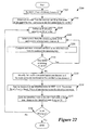
- FIG. 27 illustrates path-usage probabilities for the trees illustrated in FIGS. 13-15 .
- FIG. 28 illustrates edge-intersect counts for the trees illustrated in FIGS. 13-15 .
- FIG. 29 illustrates edge-intersect probabilities for the trees illustrated in FIGS. 13-15 .
- FIG. 30 illustrates a process that constructs one or more optimal Steiner trees for each possible net configuration with respect to a partitioning grid, and computes and stores path count and probability information.
- FIG. 31 illustrates a process for calculating the count and path-usage probabilities resulting from the Steiner trees selected by the process of FIG. 30 .
- FIG. 32 illustrates a process that pre-tabulates the length, bend-count, and path-usage values of Steiner trees that model possible net configurations within a partitioning grid.
- FIG. 33 illustrates a process that pre-tabulates one or more Steiner tree attributes for several different wiring models.
- FIG. 34 illustrates the software architecture of a placer used in some embodiments of the invention.
- FIG. 35 illustrates an IC layout that is recursively divided into sets of 16 sub-regions.
- FIG. 36 illustrates the data structure for a net list.
- FIG. 37 illustrates the data structure for a net.
- FIG. 38 illustrates the data structure of a circuit module.
- FIG. 39 presents a graph that illustrates the hierarchy of slots defined by the recursor.
- FIG. 40 presents a data structure for a slot.
- FIG. 41 illustrates a process performed by a recursor of FIG. 34 .
- FIG. 42 illustrates a process performed by an initializer of FIG. 34 .
- FIG. 43 illustrates a global path-usage data structure that stores the sum of all the path-usage values over all the nets.
- FIG. 44 illustrates an IC layout that has been partitioned into sixteen slots.
- FIG. 45 illustrates a process for generating propagated configuration codes.
- FIG. 46 illustrates a process that generates total configuration codes.
- FIG. 47 illustrates one example of a simulated annealing process.
- FIG. 48 illustrates a process that a costs estimator performs.
- FIG. 49 illustrates a process that a mover performs.
- FIG. 50 illustrates a computer system used by some embodiments of the invention.
- the invention is directed towards recursive partitioning placement method and apparatus.
- numerous details are set forth for purpose of explanation. However, one of ordinary skill in the art will realize that the invention may be practiced without the use of these specific details. In other instances, well-known structures and devices are shown in block diagram form in order not to obscure the description of the invention with unnecessary detail.
- Some embodiments of the invention calculate the cost of placement configurations for IC layouts that have diagonal interconnect lines (i.e., diagonal wiring).
- the IC layouts not only have diagonal interconnect lines, but also have horizontal and vertical interconnect lines.
- an interconnect line is “diagonal” if it forms an angle other than zero or ninety degrees with respect to the layout boundary.
- an interconnect line is “horizontal” or “vertical” if it forms an angle of 0° or 90° with respect to one of the sides of the layout.
- FIG. 9 illustrates the wiring architecture (i.e., the interconnect-line architecture) of an IC layout 900 that utilizes horizontal, vertical, and 45° diagonal interconnect lines.
- this architecture is referred to as the octagonal wiring model, in order to convey that an interconnect line can traverse in eight separate directions from any given point.
- the horizontal lines 905 are the lines that are parallel (i.e., are at 0°) to the x-axis, which is defined to be parallel to the width 910 of the layout.
- the vertical lines 915 are parallel to the y-axis, which is defined to be parallel to the height 920 of the layout.
- the vertical interconnect lines 915 are perpendicular (i.e., are at 90°) to the width of the IC layout.
- one set 925 of diagonal lines are at +45° with respect to the width of the IC layout, while another set 930 are at ⁇ 45° with respect to the width of the IC layout.
- FIG. 10 illustrates one manner of implementing the wiring architecture illustrated in FIG. 9 on an IC. Specifically, FIG. 10 illustrates five metal layers for an IC.
- the first three layers 1005 - 1015 are Manhattan layers. In other words, the preferred direction for the wiring in these layers is either the horizontal direction or the vertical direction.
- the preferred wiring direction in the first three layers typically alternates so that no two consecutive layers have the same direction wiring. However, in some cases, the wiring in consecutive layers is in the same direction.
- the next two layers 1020 and 1025 are diagonal layers.
- the preferred direction for the wiring in the diagonal layers is ⁇ 45°.
- the wiring directions in the fourth and fifth layer are typically orthogonal (i.e., one layer is +45° and the other is ⁇ 45°), although they do not have to be.
- some embodiments are used with non ⁇ 45° diagonal wiring.
- some embodiments are used with IC layouts that have horizontal, vertical, and ⁇ 120° diagonal interconnect lines.
- such a wiring architecture is referred to as the hexagonal wiring model, in order to convey that an interconnect line can traverse in six separate directions from any given point.
- FIG. 11 conceptually illustrates the operational flow of a placement-process 1100 of some embodiments of the invention. This process starts each time it receives the coordinates for a region of the IC layout.
- the received region can be the entire IC layout, or a portion of this layout.
- this process also receives a net list that specifies all the net's that have circuit elements in the received IC region. In other embodiments, the process receives a list of all the circuit elements in the received IC region, and from this list identifies the nets that have circuit elements in the received IC region.
- each received or identified net has several circuit elements associated with it (i.e., each net is defined to include several circuit elements).
- the circuit elements associated with the nets are the pins of the circuit modules in the IC layout.
- the circuit elements are the circuit modules.
- the locations of the circuit elements in the received IC region define a placement configuration within this region.
- the initial circuit-element positions before the process 1100 starts are random.
- some embodiments use a previous physical-design operation, such as the floor planning, to partially or completely specify the initial positions of these elements.
- Still other embodiments use another placer to specify the initial positions of the circuit elements in the received IC region, and then use process 1100 to optimize the placement configuration for a wiring architecture that uses diagonal wiring.
- the process 1100 initially defines (at 1105 ) partitioning lines that divide the received IC region into several sub-regions (also called slots).
- the partitioning lines are intersecting lines that define a partitioning grid.
- the intersecting partitioning lines are N horizontal and M vertical lines that divide the received IC region into (N+1)(M+1) sub-regions, where N and M can equal any integer. For instance, these horizontal and vertical lines divide the received IC region into (1) four sections when N and M equal 1, (2) nine sections when N and M equal 2, (3) sixteen sections when N and M equal 3, or (4) twenty sections when either N or M equals 4 and the other equals 5.
- FIG. 12 illustrates an IC layout 1200 that has been divided into sixteen sub-regions by sets of three horizontal and vertical partitioning lines. This figure also shows a net 1205 that includes five circuit modules 1210 , 1215 , 1220 , 1225 , and 1230 , which fall into four of the sixteen sub-regions. These four sub-regions are slots 1 , 2 , 8 , and 9 .
- the process identifies (at 1110 ), for each received or identified net, the set of sub-regions (i.e., the set of slots) that contain the circuit modules of that net.
- the identified set of sub-regions for each net represents the net's configuration with respect to the defined grid.
- the process next identifies (at 1115 ) attribute or attributes of a connection graph that models the net's configuration with respect to the grid. Specifically, for each net, the connection graph provides a topology of interconnect lines that connect the slots that contain the net's circuit modules.
- each slot that contains one or more of the net's circuit modules is treated as a node (also called a vertex or point) of the connection graph.
- the nodes of the graph are then connected by edges (also called lines).
- the connection graph can have edges that are completely or partially diagonal.
- different embodiments identify different attributes of a net's connection graph.
- the attributes can include the length of the connection graph, the number of bends in the connection graph, the probability of the connection graph intersecting the partitioning lines, etc.
- some embodiments might just identify one attribute (e.g., length) of each net's connection graph, while other embodiments might identify several attributes (e.g., length and number of bends) of each net's connection graph.
- FIG. 13-15 illustrate three optimal Steiner trees 1305 , 1405 , and 1505 for the net 1205 in FIG. 12 . These Steiner trees all have the same length. One of these trees ( 1305 ) has a Steiner node ( 1320 ). In addition, each of these trees has at least one edge that is partially diagonal. In these examples, the diagonal edges are at 45° degrees with respect to the layout boundary. When the octagonal wiring model is used, the length of these Steiner trees is an approximation of the interconnect-line length necessary for net 1205 at the current partitioning grid level.
- the process identifies (at 1115 ) the attribute or attributes of each net's connection graph by constructing this connection graph in real-time and quantifying its attribute or attributes during or after the construction of the graph.
- the embodiments described below identify the attributes of the connection graphs in a different manner.
- these embodiments (1) construct the connection graphs for each possible net configuration with respect to the partitioning grid, and (2) pre-tabulate the attributes of the connection graphs in memory. During placement, these pre-tabulating embodiments then retrieve (at 1115 ) the attribute or attributes of the connection graph of each identified net configuration from memory.
- connection graphs might pre-tabulate multiple attributes of the connection graphs (such as length, number of bends, probabilities for intersecting partitioning lines, etc.). Also, some embodiments might pre-tabulate attributes of connection graphs that are based on different wiring models. Section III below explains several processes for pre-tabulating different attributes of Steiner trees for different wiring architectures.
- the process 1100 uses the attributes identified at 1115 to calculate the cost of the placement layout within the received region. For instance, when the process identifies the probabilities of the partitioning lines being cut, some embodiments compute a congestion cost estimate based on these probabilities. Alternatively, when the identified attribute is the length of the graphs, some embodiments calculate the cost of a placement configuration within the received IC region, by combining (e.g., summing, multiplying, etc.) the length of the graphs associated with the net configurations within the received region.
- Some embodiments calculate the placement cost based on more than one type of attribute for each connection graph. For instance, some embodiments calculate the placement cost of the graphs by combining (e.g., generating a weighted sum of) the length and bend-count of the graphs. Other embodiments might combine these two attributes of a net's connection graph by using as the net's cost the length of the shortest connection graph that has less than a maximum bend count; if all the connection graphs have more than the maximum bend count, some of these embodiments use as the net's cost the length of the shortest connection graph that has less than an incremented maximum bend count.
- the process uses an optimization algorithm that iteratively modifies the placement configuration in the received IC regions, in order to improve the placement cost.
- Different embodiments of the invention use different optimization techniques, such as annealing, local optimization, KLFM, tabu search, etc.
- different optimization techniques modify the placement configuration differently. For instance, at each iteration, some techniques move one circuit module, others swap two modules, and yet others move several related modules, between the sub-regions defined at 1105 .
- some optimization techniques e.g., KLFM and tabu search algorithms
- search for the best move while others (e.g., simulated annealing and local optimization) select random moves.
- some techniques e.g., simulated annealing
- the placement configuration is re-calculated by repeating the cost-calculating operations 1110 - 1120 for all the nets or for just the nets on which the moved circuit module or modules reside.
- the process 1100 recursively performs the partitioning and optimization operations 1105 - 1125 on each sub-region defined at 1105 that meets one or more criteria. For instance, some embodiments recursively perform the partitioning and optimization operations on each sub-region that contains more than a specified number of circuit modules.
- Some embodiments use different shaped partitioning grids for different levels in the recursion process. Other embodiments use same shaped partitioning grids for all the recursion levels. At each recursion level, these embodiments simply adjust the coordinates of the partitioning grid to match the coordinates of the IC region at that recursion level. Using the same shaped partitioning grids for all the recursion levels has several advantages. For instance, it allows the pre-tabulating embodiments to store only net configuration attributes for one partitioning grid; these attributes can be re-used at all the recursion levels because they can be used to define the relative costs of the net configurations at any one level.
- FIGS. 16-33 illustrate one manner of pre-tabulating attributes of Steiner trees that model possible net configurations with respect to a partitioning grid.
- FIGS. 16 and 17 illustrate how some embodiments (1) calculate the length of an interconnect line connecting two nodes of a connection graph, and (2) detect whether this line has a diagonal bend. These embodiments perform these operations by treating the two nodes as opposing corners of a bounding box that has a long side (L) and a short side (S).
- L long side
- S short side
- FIG. 16 presents an example of a bounding-box 1605 for two nodes 1635 and 1640 .
- the line 1610 traverses the shortest distance between nodes 1635 and 1640 for IC layouts that utilize horizontal, vertical, and diagonal interconnect lines.
- This line is partially diagonal. Specifically, in this example, one segment 1620 of this line is diagonal, while another segment 1615 is horizontal.
- Equation (A) below provides the distance traversed by line 1610 (i.e., the minimum distance between the nodes 1635 and 1640 ).
- Distance [ L ⁇ S (cos A /sin A ) ⁇ ]+ S /sin A (A)
- L is the box's long side, which in this example is the box's width 1625 along the x-axis
- S is the box's short side, which in this example is its height 1630 along the y-axis.
- “A” is the angle that the diagonal segment 1620 makes with respect to the long side of the bounding box.
- this angle A corresponds to the direction of some of the diagonal interconnect lines in the IC layout. For instance, in some embodiments, the angle A equals 45° when the IC layout uses the octagonal wiring model. In this manner, the diagonal cut 1620 across the bounding box represents a potential diagonal interconnect line that forms the connection between the two nodes.
- Equations (B)-(D) below illustrate how Equation (A) is derived.
- the length of the line 1610 equals the sum of the lengths of its two segments 1615 and 1620 .
- Equation (B) provides the length of the horizontal segment 1615
- Equation (C) provides the length of the diagonal segment 1620 .
- Length of 1615 L ⁇ (Length of 1620 )*(cos A )
- the bounding box When the bounding box has no width or height, then the bounding box is just a line, and the minimum distance between the opposing corners of this line is provided by the box's long (and only) side, which will be a horizontal or vertical line.
- the bounding box has equal sized height and width (i.e., when it is a square) and the angle A is 45°, a line that is completely diagonal specifies the shortest distance between the box's two opposing corners.
- a line that has a diagonal bend i.e., a line that has a diagonal component and a vertical or horizontal component
- the minimum distance computed by Equation (A) is an approximation of the shortest length of wiring required to connect two hypothetical modules or pins represented by the nodes 1635 and 1640 . This distance might be shorter than the actual wiring path necessary for connecting the two nodes, as it may not be possible to route the net along line 1610 .
- the distance value computed by Equation (A) simply provides a lower-bound estimate on the interconnect-line length required to connect the two nodes in a wiring architecture that utilizes horizontal, vertical, and diagonal wiring. Some embodiments also use this equation for other arbitrary wiring models. However, some of these embodiments select the angle A among several choices so that the distance quantified by this equation is minimized.
- FIG. 17 illustrates a process 1700 that (1) identifies a bounding box for two nodes of a connection tree, (2) calculates the length of an interconnect line connecting the two nodes based on the bounding box's dimensions and Equation (A), and (3) detects whether the interconnect line has a diagonal bend.
- This process initially (at 1705 ) determines whether the x-coordinate (X 1 ) of the first node is greater than the x-coordinate (X 2 ) of the second node. If so, the process defines (at 1710 ) the x-coordinate (X 1 ) of the first node as the maximum x-coordinate (X Max ), and the x-coordinate (X 2 ) of the second node as the minimum x-coordinate (X Min ). Otherwise, the process defines (at 1715 ) the x-coordinate (X 2 ) of the second node as the maximum x-coordinate (X Max ), and the x-coordinate (X 1 ) of the first node as the minimum x-coordinate (X Min ).
- the process determines (at 1720 ) whether the y-coordinate (Y 1 ) of the first node is greater than the y-coordinate (Y 2 ) of the second node. If so, the process defines (at 1725 ) the y-coordinate (Y 1 ) of the first node as the maximum y-coordinate (Y Max ), and the y-coordinate (Y 2 ) of the second node as the minimum y-coordinate (Y Min ). Otherwise, the process defines (at 1730 ) the y-coordinate (Y 2 ) of the second node as the maximum y-coordinate (Y Max ), and the y-coordinate (Y 1 ) of the first node as the minimum y-coordinate (Y Min ).
- the process then defines (at 1735 ) the four coordinates of the bounding box as (X MIN , Y MIN ), (X MIN , Y MAX ), (X MAX , Y MIN ), and (X MAX , Y MAX ).
- the process determines (at 1740 ) the bounding-box's width and height. The process determines (1) the width by taken the difference between the box's maximum and minimum x-coordinates, and (2) the height by taking the difference between the box's maximum and minimum y-coordinates.
- the process determines (at 1745 ) whether the computed width is greater than the computed height. If so, the process defines ( 1750 ) the width as the long side and the height as the short side. Otherwise, the process defines (at 1755 ) the width as the short side and the height as the long side.
- the process uses (at 1760 ) the above-described Equation (A) to compute the length of the shortest interconnect line that connects the two nodes. The process then determines whether the interconnect line has a diagonal bend. Even though the process 1700 only counts the diagonal bends, other embodiments count other types of bends (e.g., 90° bends from horizontal to vertical lines), especially when non-octagonal wiring architectures are used.
- the process 1700 To determine whether the interconnect line has a diagonal bend, the process 1700 initially determines (at 1765 ) whether the long or short side of the computed bounding box equals zero. If so, the interconnect line is a vertical or horizontal line that does not have a diagonal bend, and thereby the process sets (at 1770 ) the bend value of this line to zero.
- the process determines (at 1775 ) whether the interconnect line is purely diagonal.
- the angle A in Equation (A) is defined to be 45° or less
- the process determines whether the interconnect line is purely diagonal by ascertaining whether the arctan of the bounding box's short side divided by its long side equals the angle A.
- the angle A in Equation (A) is defined to be more than 45°
- the process determines whether the interconnect line is purely diagonal by ascertaining whether the arctan of the bounding box's long side divided by its short side equals the angle A.
- the process determines that the interconnect line is purely diagonal, then the process sets (at 1770 ) the bend value of this line to zero as this line has no diagonal bend. Otherwise, the interconnect line has a diagonal bend (i.e., it has a diagonal segment and a vertical or horizontal segment), and therefore the process sets (at 1780 ) the bend value of this line to 1. After 1770 or 1780 , the process ends.
- FIG. 18 illustrates a process 1800 that (1) constructs Steiner trees for each possible net configuration with respect to a partitioning grid, and (2) stores the length and/or diagonal bend-count of each constructed Steiner tree in a look-up table (“LUT”).
- LUT look-up table
- process 1800 initially starts (at 1805 ) by defining a Steiner-tree node for each sub-region (also called slot) defined by a particular partitioning grid.
- FIG. 19 pictorially illustrates sixteen Steiner-tree nodes 1905 for sixteen slots created by a 4-by-4 partitioning grid. These nodes represent all the potential nodes of Steiner trees that model the interconnect topologies of all the net configurations.
- the identified nodes are positioned at the center of each slot. In other embodiments, the nodes can uniformly be defined at other locations in the slots (e.g., can be uniformly positioned at one of the corners of the slots).
- the process 1800 defines (at 1810 ) a set N of possible node configurations.
- set N includes 2 Y node configurations.
- the process 1800 select (at 1815 ) one of the possible node configurations N T from this set.
- FIG. 20 illustrates one possible configuration, which includes nodes 2010 , 2015 , 2020 , and 2025 . This node configuration coincides with the node configuration for the net 1205 illustrated in FIG. 12 .
- the process then constructs (at 1820 ) a minimum spanning tree (“MST”) for the node configuration selected at 1815 , and computes this tree's length (MST_Cost) and diagonal bend-count (Bend_Cost).
- MST_Cost minimum spanning tree
- Bend_Cost diagonal bend-count
- FIG. 21 illustrates a process 2100 for identifying potential Steiner nodes. This process starts (at 2105 ) by initializing a set P of potential Steiner nodes equal to all the nodes defined at 1805 that are not part of the node configuration selected at 1815 . This process then selects (at 2110 ) one of the potential Steiner nodes.
- the process 2100 determines (at 2115 ) whether the node (Q) selected at 2110 is on a shortest path between any two nodes in the selected node configuration. To make this determination, the process determines whether any two nodes (B and C) exit in the node configuration such that the distance between the two nodes (B and C) equals the sum of (1) the distance between the first node (B) and the selected node (Q), and (2) the distance between the second node (C) and the selected node (Q). In some embodiments, the process uses the above-described process 1700 and Equation (A) to calculate the distance between any pair of nodes.
- the process determines that the node Q selected at 2110 lies on a shortest path between any two nodes in the node configuration, the process keeps (at 2120 ) the selected node in the set P of potential Steiner nodes, flags this node as a node that it has examined, and transitions to 2130 , which is described below.
- the process removes (at 2125 ) the selected node from the set P of potential Steiner nodes, and transitions to 2130 .
- the process determines whether it has examined all the nodes in the set of potential Steiner nodes. If not, the process returns to 2110 to select another node in this set so that it can determine at 2115 whether this node is on a shortest path between any two nodes in the selected node configuration. When the process determines (at 2130 ) that it has examined all the nodes in the set of potential Steiner nodes, it ends.
- FIG. 20 pictorially illustrates the result of performing process 2100 for the node configuration 2005 .
- this figure illustrates several potential Steiner nodes 2050 , and several non-Steiner nodes 2055 .
- the process 2100 initially defines the set of potential Steiner nodes to include all the nodes 2050 and 2055 that are not in the node configuration 2005 .
- the process then removes the nodes 2055 from this set as these nodes do not lie on the shortest path between any two nodes in the selected node configuration.
- each defined set of Steiner nodes includes one or more of the Steiner nodes identified at 1825 . Also, each defined set of Steiner nodes has a maximum size that is two nodes less than the number of nodes in the selected node configuration.
- the process 1800 selects (at 1835 ) one of the Steiner-node sets defined at 1830 .
- the process then (at 1840 ) (1) constructs a minimum spanning tree (MST) for the nodes in the selected node configuration and the selected Steiner-node set, and (2) computes and stores this MST's length (MST_Cost) and diagonal bend-count (Bend_Cost).
- MST_Cost minimum spanning tree
- Bend_Cost diagonal bend-count
- the process determines (at 1845 ) whether, in the Steiner node sets defined at 1830 , there are any additional Steiner-node sets that it has not yet examined. If so, the process returns to 1835 to select another Steiner-node set, so that it can construct a MST for the nodes of this set and the nodes in the selected node configuration.
- the process uses (at 1850 ) a selection criterion to select one of the MST's generated at 1820 and 1840 as the Steiner tree for the current node configuration (i.e., the node configuration selected at 1815 ).
- the process 1800 uses different selection criteria. For instance, in some embodiments, the process selects (at 1850 ) the MST with the smallest length (i.e., the MST with the smallest MST_Cost stored at 1820 and 1840 ).
- the process uses both the length and bend-count values to formulate a selection criterion or criteria. For instance, some embodiments select the shortest MST that has less than a maximum number of bends (e.g., the shortest MST that has less than two diagonal bends). If all the generated MST's have more than the maximum bend count, some of these embodiments select the shortest MST that has less than an incremented maximum bend count (e.g., the shortest MST that has less than three diagonal bends).
- a maximum number of bends e.g., the shortest MST that has less than two diagonal bends.
- each generated MST's length and bend-count e.g., generate a weighted sum of the MST_Cost and the Bend_Cost
- combine each generated MST's length and bend-count e.g., generate a weighted sum of the MST_Cost and the Bend_Cost to obtain a combined score, based on which they select one of the MST's.
- the process then stores (at 1855 ) in a storage structure (such as a LUT) the length (MST_Cost) and bend-count (Bend_Cost) of the Steiner tree identified at 1850 .
- a placer can then quickly identify the length and bend-count of the Steiner tree for the current node configuration by retrieving the stored length and bend-count from the storage structure.
- the process next determines (at 1860 ) whether it has examined all the node configurations in the set N defined at 1810 . If not, the process returns to 1815 to select unexamined node configuration from this set and then repeat operations 1820 - 55 to determine and store the Steiner length and bend-count for this node configuration. Otherwise, the process ends.
- FIG. 22 illustrates a process 2200 that the process 1800 of FIG. 18 uses at 1820 and 1840 to construct minimum spanning trees.
- a minimum spanning tree for a node configuration is a tree that has N- 1 edges that connect (i.e., span) the N nodes of the configuration through the shortest route, which only branches (i.e., starts or ends) at the nodes.
- the length of a MST for a net configuration provides a lower-bound estimate of the amount of wire needed to interconnect the nodes associated with the net configuration.
- the edges of the MST's can be horizontal, vertical, or diagonal.
- the diagonal edges can be completely or partially diagonal.
- the diagonal edges of the MST's can be in the same direction (e.g., can be in ⁇ 120° direction) as some of the diagonal interconnect lines in the layout.
- FIG. 23 illustrates an example of such a MST.
- This tree 2305 is the MST of the net that contains pins 135 , 145 , and 160 of FIG. 1 .
- This tree has two edges 2310 and 2315 .
- the first edge 2310 has a horizontal segment 2320 and a +45° diagonal segment 2325
- the second edge 2315 has a vertical segment 2330 and a ⁇ 45° diagonal segment 2335 .
- the length of each edge can be obtained by using the above-described process 1700 and Equation (A).
- Distance [ L ⁇ S (cos A /sin A ) ⁇ ]+ S /sin A (A)
- L is the box's long side
- S is the box's short side
- A is the angle that the diagonal segment of the edge makes with respect to the long side of the bounding box.
- the process 2200 starts whenever the process 1800 calls it (at 1820 or 1840 ) (1) to construct an MST for a set M of nodes, and (2) to calculate the length and bend-count of this MST.
- This process initially (at 2205 ) sets the MST length (MST_Cost) and bend count (Bend_Cost) to zero.
- the process (1) selects a node from the received set M of nodes as the first node of the spanning tree, and (2) removes this node from this set M.
- the process then defines (at 2215 ) a remainder set R of nodes equal to the current set M of nodes.
- the process selects a node from the remaining node set R, and removes the selected node from the set of remaining nodes.
- the process then computes and stores (at 2225 ) the distance between the node selected at 2220 and each current node of the spanning tree. The distance between the selected node and each node can be traversed by an edge that is completely or partially diagonal.
- the process uses the above-described process 1700 and Equation (A) to compute the minimum distance between the selected node and each node.
- the process 1700 not only computes the length of the line that traverses this minimum distance, but also computes the bend value for this line.
- the process determines (at 2230 ) whether there is any node remaining in set R. If so, the process returns to 2220 to select another node from this set, so that it can compute (at 2225 ) the distance between this node and the current nodes of the spanning tree. Otherwise, the process (at 2235 ) identifies the smallest distance recorded at 2225 , and identifies the node combination (i.e., the node in set M and the MST's node) that resulted in this distance. The process then (at 2240 ) (1) adds the identified smallest distance to the MST length (MST_Cost), and (2) increments the MST bend count (Bend_Cost) by the bend value of the line that traverses this distance.
- MST_Cost MST length
- Bend_Cost increments the MST bend count
- the process next (at 2245 ) (1) defines a tree node corresponding to the node identified at 2235 , (2) removes the identified node from the node set M, and (3) links the defined tree node to the MST node identified at 2235 .
- the process determines (at 2250 ) whether the node set M is empty. If not, the process transitions back to 2215 to identify the next node (in this set M) that is closest to the current nodes of the MST. Otherwise, the process determines that it has constructed the MST for the received set M of nodes, returns the computed MST length (MST_Cost) and bend count (Bend_Cost) for this set, and then ends.
- Section III.A.2 pre-tabulate length and/or bend-count values of Steiner trees that model net configurations with respect to a partitioning grid. Other embodiments, however, pre-tabulate other attributes of these trees. For instance, some embodiments pre-tabulate information about the directed-wiring paths (also called directed routing or interconnect-line paths) that these trees use in the partitioning grid. As further described below, the stored wiring-path information can be used during placement to quantify wiring congestion (also called routing or interconnect-line congestion) of a particular placement configuration.
- directed-wiring paths also called directed routing or interconnect-line paths
- the stored wiring-path information can be used during placement to quantify wiring congestion (also called routing or interconnect-line congestion) of a particular placement configuration.
- the number of directed-wiring paths in a partitioning grid depends on the wiring model and the number of partitioning lines in the grid. For instance, 42 directed-wiring paths exist when the octagonal wiring architecture is used in combination with a 4 ⁇ 4 grid. Specifically, the combination of the octagonal wiring architecture and the 4 ⁇ 4 grid results in 42 edges between the slots of the 4 ⁇ 4 grid.
- FIG. 24 illustrates these 42 edges (E 1 -E 42 ). Orthogonal to each particular edge is a directed-wiring path that specifies the direction of the interconnect lines that connect the two slots abutting the particular edge. As there are 42 edges in a 4 ⁇ 4 grid that uses the octagonal wiring model, there are 42 directed-wiring paths in these circumstances.
- FIG. 25 illustrates the 42 directed-wiring paths (P 1 -P 42 ) across the 42 edges (E 1 -E 42 ) of FIG. 24 .
- directed-wiring paths do not necessarily specify the actual routing paths used during routing.
- directed-wiring path P 28 in FIG. 25 does not necessarily have to specify the one and only routing path between the fifth and sixth slots, as routing paths can traverse the entire length of edge E 28 . Instead, the directed-wiring paths only specify the direction of the interconnect lines that connect the two slots abutting the particular edge.
- the wiring-path information for each net configuration can be stored as an N-bit string or in an N-entry data structure (e.g., N-entry array), where N is the number of wiring directions that result from a particular combination of partitioning grid and wiring model.
- N is the number of wiring directions that result from a particular combination of partitioning grid and wiring model.
- each net configuration's wiring-path information can be stored in a 42-bit string or 42-entry array.
- Different embodiments store different directed-wiring path information.
- Some embodiments identify only one of routing pattern (e.g., one Steiner tree) for each net configuration. Hence, for each net configuration, these embodiments only store the identity of the directed-wiring paths used by the net configuration's selected routing pattern.
- such an identify can be stored as an N-bit string, where each bit in this string corresponds to one of the directed-wiring paths and each particular bit is set when the identified routing pattern uses the directed-wiring path corresponding to the particular bit. For instance, if (1) the routing pattern 1305 of FIG. 13 is selected to connect the node configuration of net 1205 of FIG. 12 and (2) the numbering convention of FIG.
- the wiring-path information for the selected routing pattern 1305 is a 42-bit string that has its 17 th , 31 st , 32 nd , 36 th , and 40 th bits set (e.g., set to 1) and all the other bits not set (e.g., equal to 0).
- Some embodiments enumerate several routing patterns for each net configuration within the partitioning grid. For instance, some embodiments identify the optimal Steiner trees for each net configuration. It is advantageous to enumerate and store information about all the optimal routing patterns when the exact routing pattern for each net configuration is not selected during placement. In this manner, the placer can account for all the congestion that can potentially result from each net configuration.
- the embodiments that identify several routing patterns for each net configuration can store different types of information about the directed-wiring paths used by these routing patterns. For instance, some of these embodiments count and store the number of times each directed-routing path in the grid is used by the identified optimal trees of each net configuration. For each net configuration, such count information can be stored in an N-entry data structure, where each entry stores the count information for one of the directed-wiring paths.
- Steiner trees 1305 , 1405 , and 1505 of FIGS. 13-15 provide the optimal routing patterns for the node configuration of net 1205 of FIG. 12 when the octagonal wiring model is used. As illustrated in FIG. 26 , these trees (1) use the directed-wiring paths 17 , 31 - 33 , 37 , and 41 once, (2) use the directed-wiring paths 14 , 27 and 36 twice, and (3) use the directed-wiring path 40 thrice. This count information can be stored in a 42-entry array, where each entry corresponds to one of the wiring paths.
- the entries for the 17 th , 31 st -33 rd , 37 th , and 41 st paths are set to 1
- the entries for the 14 th , 27 th , and 36 th paths are set to two
- the entries for the 40 th path is set to 3
- the entries for all other paths are set to 0.
- embodiments do not store the number of times each directed-routing path in the grid is used by the identified trees of each net configuration. For instance, some embodiments store the probability that the identified trees of a net configuration use each directed-routing path. For each directed-routing path, this probability can be obtained by dividing the number of times the identified trees use the directed-routing path by the total number of identified trees.
- FIG. 27 illustrates these probabilities for the directed-routing paths used by the Steiner trees 1305 , 1405 , and 1505 of FIGS. 13-15 .
- These probabilities are obtained by dividing the count information (illustrated in FIG. 26 ) for these directed-routing paths by 3, which is the number of the identified routing trees.
- these probabilities are (1) 0.33 for the directed-wiring paths 17 , 31 - 33 , 37 , and 41 , (2) 0.66 for the directed-wiring paths 14 , 27 and 36 , (3) 1 for the directed-wiring path 40 , and (4) 0 for the remaining directed-wiring paths.
- This probability information can be stored in a 42-entry array, where each entry corresponds to one of the wiring paths.
- the entries for the 17 th , 31 st -33 rd , 37 th , and 41 st paths are set to 0.33
- the entries for the 14 th , 27 th , and 36 th paths are set to 0.66
- the entries for the 40 th path is set to 1
- the entries for all other paths are set to 0.
- the placer can calculate congestion cost estimates for different placement configurations by using the pre-tabulated wiring-path information. To calculate such a congestion cost, the placer for each net (1) identifies the net's configuration with respect to the partitioning grid, and then (2) retrieves the pre-tabulated wiring-path information, which includes one value for each wiring path in the grid.
- Cost max Path ⁇ ( ⁇ nets ⁇ F ⁇ ( netconfig , path ) ) ( G )
- Yet other embodiments use other approaches to compute placement cost estimates based on the wiring-path values. For instance, instead of summing the retrieved values for each particular wiring path over all the nets, some embodiments might combine these values associated with each wiring path in a different manner (e.g., some might multiply the values associated with each wiring path).
- the above-described embodiments pre-tabulate wiring-path information.
- Other embodiments pre-tabulate edge-intersect information, instead of wiring-path information. Storing the edge-intersection information is analogous to storing the wiring-path information, since each wiring path is defined across a particular edge, as illustrated by FIGS. 24 and 25 .
- Some embodiments identify the edge-intersect information for a net configuration by (1) defining edges in the partitioning grid based on the grid and the wiring model, (2) specifying one or more connection graphs (such as Steiner trees) for each net configuration within the grid, and (3) identifying the edges that the specified graphs intersect.
- connection graphs such as Steiner trees
- the embodiments that identify only one routing pattern (e.g., one Steiner tree) for each net configuration can store for each net configuration the identity of the edges intersected by the net configuration's selected routing pattern.
- such an identify can be stored as an N-bit string, where each bit in this string corresponds to one of the edges and each particular bit is set when the identified routing pattern intersects the edge corresponding to the particular bit. For instance, if (1) the routing pattern 1305 of FIG. 13 is selected to connect the node configuration of net 1205 of FIG. 12 and (2) the numbering convention of FIG.
- the edge-intersect information for the selected routing pattern 1305 is a 42-bit string that has its 17 th , 31 nd , 32 nd , 36 th , and 40 th bits set (e.g., set to 1) and all the other bits not set (e.g., equal to 0).
- some of the embodiments that enumerate several routing patterns for each net configuration count and store the number of times each edge is used by the enumerated routing patterns of the net configuration.
- other embodiments store the probability that the enumerated trees for the net configuration intersect the edge. This probability can be obtained by dividing the number of times the identified trees intersect the edge by the total number of identified trees.
- FIGS. 28 and 29 respectively illustrate the count and probability information for the Steiner trees 1305 , 1405 , and 1505 of FIGS. 13-15 that provide routing patterns for the node configuration of net 1205 of FIG. 12 .
- the count or probability information can be stored in an N-entry data structure, where N corresponds to the number of edges and each entry stores the count or probability information for one of the edge.
- the count information for trees 1305 , 1405 , and 1505 can be stored in a 42-entry array, with the entries for the 17 th , 31 st -33 rd , 37 th , and 41 st edges set to 1, the entries for the 14 th , 27 th , and 36 th edges set to two, the entries for the 40 th edge set to 3, and the remaining entries set to 0.
- the probability information for these trees can be stored in a 42-entry array, with entries for the 17 th , 31 st -33 rd , 37 th , and 41 st edges set to 0.33, the entries for the 14 th , 27 th , and 36 th edges set to 0.66, the entries for the 40 th edge set to 1, and the entries for the remaining edges set to 0.
- a placer can calculate congestion cost estimates based on the edge-intersection information similarly to how it would calculate such estimates based on the wiring-path information. Specifically, to calculate such a congestion cost, the placer initially for each net (1) identifies the net's configuration with respect to the partitioning grid, and then (2) retrieves the pre-tabulated edge-intersection information, which includes one value for each edge in the grid.
- Cost max edge ⁇ ( ⁇ nets ⁇ F ⁇ ( netconfig , edge ) ) ( I )
- Yet other embodiments use other approaches to compute placement cost estimates based on the edge-intersect values. For instance, instead of summing the retrieved values for each particular edge over all the nets, some embodiments might combine these values associated with each edge in a different manner (e.g., some might multiply the values associated with each edge).
- FIG. 30 illustrates a process 3000 that (1) constructs one or more optimal Steiner trees for each possible net configuration with respect to a partitioning grid, (2) computes count and probability of the trees using each interconnect-line path in the grid, and (3) stores the computed count and path-usage probabilities in a storage structures (such as a LUT).
- This process is performed before the placement process 1100 of FIG. 11 , so that the placement process in real-time does not have to construct the Steiner trees and determine the path-usage probabilities for each net configuration.
- some embodiments define the set of interconnect-line paths in the grid based on the grid and on the wiring model used. For instance, as described above, some embodiments define 42 edges for using the octagonal wiring model in a 4 ⁇ 4 grid.
- the process 3000 is identical to process 1800 of FIG. 18 , except for two operations 3005 and 3010 .
- Operations 1805 - 1845 and 1860 of process 3000 are identical to similarly numbered operations 1805 - 1845 and 1860 of process 1800 .
- these operations 1805 - 1845 and 1860 will not be further described below, in order not to obscure the description of the invention with unnecessary detail.
- FIGS. 19-22 are equally applicable for the process 3000 .
- the process 3000 (1) calls process 2100 at 1825 to identify potential Steiner nodes, and (2) calls process 2200 at 1820 and 1840 to construct MST's for particular sets of nodes.
- process 1800 differs between process 1800 and process 3000 in that, unlike the process 1800 that identifies one MST at 1850 as the current node configuration Steiner tree, the process 3000 at 3005 selects one or more of the MST's generated at 1820 or 1840 as the optimal Steiner trees for the current node configuration.
- the process 3000 selects one or more Steiner trees (at 3005 ) because it is designed to help enumerate all potential congestion that can result from a particular node configuration.
- This process selects its set of Steiner trees for the current node configuration based on one or more criteria. For instance, in some embodiments, this process selects the shortest MST's as the Steiner trees (i.e., the process only uses length as a selection criterion). In other embodiments, this process uses both the length and bend-count of the MST's to select its set of Steiner trees. For example, some embodiments might select the shortest MST's that have less than a pre-specified number of bends as the Steiner trees; if none of the MST's have less than the pre-specified number of bends, these embodiments increment the minimum bend count and then select the shortest MST's with that have less than the incremented pre-specified number of bends.
- the process 3000 calls (at 3010 ) a process 3100 of FIG. 31 to calculate the count and path-usage probabilities resulting from the selected Steiner trees.
- this process starts when process 3000 calls it at 3010 and supplies it with a set of Steiner trees (i.e., one or more Steiner trees).
- the process 3100 starts by initializing (at 3105 ) the count values for each path to 0.
- the process selects (at 3110 ) a received Steiner tree, and selects (at 3115 ) one of the edges in the tree (i.e., selects a pair of linked nodes in the tree, where these nodes were linked at 2245 of FIG. 22 ).
- the process retrieves (at 3120 ) values for possible paths that this tree uses.
- the process retrieves these values from a LUT that stores path-usage values for any combination of the tree slot nodes. In other words, this LUT maps the endpoints of each possible tree edge within the grid to a set of path-usage values.
- the path-usage values in the LUT might specify values for multiple optimal routes.
- the retrieved usage value for a particular path might be greater than 1 to indicate that more than one optimal route use the particular path to connect the node pairs selected at 3115 .
- the process 3000 would identify two sets of node connections as two possible Steiner trees.
- One set of node connections e.g., node 1310 -node 1315 -Steiner node 1320 -node 1325 -node 1330
- another node connection e.g., node 1325 -node 1310 -node 1315 -node 1335
- Steiner tree of FIG. 14 or 15 could represent either the Steiner tree of FIG. 14 or 15 .
- the mapping LUT would return a 42 values, with all the values equal to 0 except the value for the path between the selected node pair. This non-zero value would be 1 to indicate that only one route exists between the selected node pair.
- the mapping LUT would return 38 path values equal to 0, and 4 path values equal to 1. Two of the four values would correspond to the paths 33 and 36 used by the Steiner tree 1405 , while the other two values would correspond to paths 37 and 41 used by Steiner tree 1505 .
- the mapper stores a path usage-value greater than one for the particular path. For example, when the selected node pairs are the node for slot 1 and the node for slot 14 (according to the numbering convention of FIG. 12 ), the mapper would store a 2 for the path 27 (i.e., the path between slots 1 and 5 ), since two of the three optimal routes between nodes 1 and 14 use this path.
- the process increments (at 3125 ) count of the paths based on the retrieved values.
- the process determines (at 3130 ) whether it has examined the last edge of the current tree (i.e., whether it has examined the last linked node pair in the current tree). If not, the process transitions back to 3115 to select the next tree edge (i.e., the next linked node pair) and to repeat 3120 and 3125 for this next tree edge.
- the process determines (at 3130 ) that it has examined the last tree edge, it then determines ( 3135 ) whether it has examined the last tree supplied by the process 3000 . If not, the process returns to 3110 to select another tree and then determine the path-usage for this tree. Otherwise, the process records (at 3140 ) the usage count for each path. Also, for each particular path, the process (at 3140 ) (1) divides the usage count by the number of the received trees to obtain the usage probability value of the particular path, and then (2) stores this resulting probability value. The process then ends.
- FIG. 32 illustrates a process 3200 that pre-tabulates the length, bend-count, and path-usage values of such Steiner trees.
- This process 3200 is a combination of the process 1800 of FIG. 18 and the process 3000 of FIG. 30 . It includes all the operations 1805 - 1845 of the processes 1800 and 3000 , operations 1850 and 1855 of the process 1800 , and operations 3005 and 3010 of the process 3000 . As these operations were described above, they will not be further described below, in order not to obscure the description of the invention with unnecessary detail. Pre-tabulating the length, bend-count, and path-usage values allows the placer to make placement designs based on any one of these attributes or any combination of these attributes.
- FIG. 33 illustrates a process 3300 that performs the process 1800 , the process 3000 , or the process 3200 once (at 3305 ) for the octagonal wiring model, once (at 3310 ) for the hexagonal wiring model, and once (at 3315 ) for the Manhattan wiring model.
- this process calculates (at 3305 ) the length, bend-count, and/or path-usage values of Steiner trees with potential 45° diagonal edges.
- the process 3300 uses 45° as the angle A in Equation (A) that process 2100 and 2200 of process 1800 , process 3000 , and process 3200 use.
- this process calculates (at 3310 ) the length, bend-count, and/or path-usage values of Steiner trees with potential 120° diagonal edges.
- the process 3300 uses 120° as the angle A in Equation (A) that process 2100 and 2200 of process 1800 , process 3000 , and process 3200 use.
- these embodiments calculate (at 3315 ) the length, bend-count, and/or path-usage values of Manhattan Steiner trees.
- the process 3300 uses 90° as the angle A in Equation (A) that process 2100 and 2200 of process 1800 , process 3000 , and process 3200 use.
- FIG. 34 illustrates the software architecture of a placer 3400 of some embodiments of the invention.
- This software architecture includes several software modules 3405 and several data constructs 3410 .
- the software modules include a recursor 3415 , an initializer 3420 , an optimizer 3425 , a cost estimator 3430 , and a mover 3435 , while the data constructs 3410 include LUT's 3440 , circuit modules 3445 , net list 3450 , nets 3455 , and slots 3460 .
- the recursor 3415 defines partitioning grids that recursively divide the IC layout into smaller and smaller sub-regions.
- the recursor uses different shaped partitioning grids for different recursion levels. In the embodiments described below, however, the recursor uses the same shaped partitioning grids for all the recursion levels. At each recursion level, the recursor simply adjusts the coordinates of the partitioning grid to match the coordinates of the IC region at that recursion level.
- Using the same shaped partitioning grids for all the recursion levels has several advantages. For instance, it allows the placer 3400 to use one set of pre-tabulated net-configuration attributes for all the recursion levels, as this set could be used to define the relative costs of the net configurations at any one level.
- the recursor uses 3 evenly-spaced horizontal lines and 3 evenly-spaced vertical lines to recursively divide IC-layout regions into 16 identically-sized sub-regions (i.e., 16 identically-sized slots).
- FIG. 35 illustrates an IC layout 3505 that is recursively divided into sets of 16 sub-regions. Specifically, the IC layout is divided initially into 16 sub-regions, each of these sub-regions is further divided into 16 smaller sub-regions, and one of the smaller sub-regions 3510 is further sub-divided into 16 sub-regions.
- the initializer 3420 calculates the placement cost of the initial placement configuration within that level's IC region. The initializer calculates this cost by first calculating initial configuration and balance costs, and then using these costs to calculate the initial placement cost.
- the placement cost has two components, the configuration cost and the balance cost.
- the configuration cost is the cost associated with the placement configuration of the nets with respect to that level's partitioning grid. This cost is computed based on attributes (such as wirelength, bend-count, path-usage, edge-intersect, etc.) of connection graphs that model the net configurations. As described below, these attributes are pre-tabulated and stored in LUT's 3440 .
- the balance cost at each recursion level reflects the size of the circuit modules in each sub-region defined by that level's partitioning grid. Hence, by factoring the balance cost, a placer can prevent some sub-regions from being excessively full.
- the embodiments described below calculate the balance cost based on (1) the capacity of each slot at that level, and (2) the size of circuit modules within each slot. Also, at each recursion level, these embodiments calculate the configurations costs by (1) identifying each net's configuration with respect to that level's partitioning grid, (2) using each net's configuration to retrieve pre-tabulated attributes from the LUT's, and (3) computing a configuration cost based on the retrieved attribute or attributes for the net configurations.
- the optimizer 3425 After the initializer 3420 calculates the placement cost of the initial placement configuration within a recursion level's IC region, the optimizer 3425 then iteratively modifies the placement configuration to improve the placement cost within that region. For each potential move that the optimizer selects, the optimizer uses the cost estimator 3430 to calculate the placement cost of the move.
- the optimizer then analyzes these costs to determine whether to make the move. If it decides to make the move, the optimizer uses the mover 3435 to modify the placement configuration according to the selected move.
- FIGS. 41-49 further describe the software modules 3405 . However, before describing these software modules, the data constructs 3410 will be described below by reference to FIGS. 36-40 .
- the LUT's 3440 store placement attributes for all possible net configurations. Specifically, some embodiments store in the LUT's attributes of Steiner trees that model the interconnect topologies of the net configurations (i.e., that model the topologies of the interconnect lines connecting the sub-regions that contain the circuit modules of the nets). In some embodiments of the invention, the Steiner trees have edges that are completely or partially diagonal.
- the LUT's store the length and path-usage values of the Steiner trees for all possible net configurations. Some of these embodiments also consider the bend-count values of the trees during pre-tabulation of the length or path-usage values by using the bend-count values as one of the factors for selecting the trees. Other embodiments, however, store the bend-count values for the trees instead of, or in addition to, the length and path-usage values.
- Several processes for selecting Steiner trees and pre-tabulating their length, bend-count, and path-usage values were discussed above in Section III. One of ordinary skill will understand that other embodiments also store other attributes of trees.
- Some embodiments calculate the configuration cost of the Steiner trees by combining (e.g., generating a weighted sum of) multiple attributes (e.g., length, bend-count, etc.) of the trees. Such a calculation can be performed during the pre-tabulating process or during the placement process.
- the placer 3400 can operate with different wiring architectures.
- different LUT's can be used to store the configuration attributes for the different wiring models. For instance, when the IC layout uses the octagonal wiring model, one of the LUT's 3440 stores the length, bend-count, and/or path-usage values of Steiner trees that can have 45° diagonal edges. Alternatively, when the IC layout uses the hexagonal wiring model, one of the LUT's stores the length, bend-count, and/or path-usage values of the Steiner trees that can have 120° diagonal edges. One of the LUT's can also store length, bend-count, and/or path-usage values for rectilinear Steiner trees, i.e., Steiner trees that only use horizontal and vertical lines.
- each LUT is a table of floating point numbers. Each table is indexed by a configuration code. In other words, to retrieve configuration attribute for a particular net configuration, the configuration code for the net configuration is identified, and this configuration code is used to identify the entry in the LUT that stores the net's configuration attribute.
- the configuration code is a 16-bit number, where each bit represents a sub-region defined by the current partitioning grid. Specifically, in some embodiments, each configuration-code bit is set (e.g., equals 1) when the associated net has a circuit module in the sub-region represented by the configuration-code bit, and is not set (e.g., equals 0) when the associated net does not have a circuit module in this sub-region. Also, in these embodiments, there are 2 16 configuration codes that represent the 2 16 possible net configurations.
- FIG. 36 illustrates the data structure for a net list 3600 .
- each net data structure is a net data object (i.e., an instantiation of a net data class).
- the net list includes several fields 3605 . Each field refers (e.g., points) to a net 3610 .
- FIG. 37 illustrates the data structure for a net.
- each net data structure is a net data object (i.e., an instantiation of a net data class).
- Each net data structure 3610 includes a field 3705 that stores the net's configuration code.
- each net's configuration code is a 16-bit number that describes the net's configuration with respect to that stage's partitioning grid.
- Each bit in the configuration code represents one of sixteen sub-regions defined by a partitioning grid.
- each configuration-code bit is set to 1 when the associated net has a circuit module in the sub-region represented by the configuration-code bit, and is set to 0 when the associated net does not have a circuit module in this sub-region.
- the configuration code is 1100000110000000 for the net 1205 with respect to the partitioning grid 1200 of FIG. 12 .
- This code reflects that this net has circuit modules in the 1, 2, 8, and 9 sub-regions defined by partitioning grid 1200 .
- the net's code configuration within that grid is represented by a string of 16 zeros.
- the net data structure 3610 also includes a field 3710 that refers (e.g., points) to a distribution array 3715 .
- the distribution array 3715 is defined with respect to the partitioning grid for that stage. This array includes 16 integer entries. Each entry corresponds to a partitioned sub-region defined by the recursor 3415 , and specifies the number of the net's circuit modules in its corresponding sub-region. For instance, the distribution array for net 1205 with respect to the partitioning grid 1200 is illustrated below.
- the initializer 3420 each time the recursor defines a new partitioning grid that divides a particular IC region into 16 smaller sub-regions, the initializer 3420 (1) records in each net's data structure a configuration code that represents the net's initial configuration within the newly partitioned region, and (2) records in each net's distribution array the count of the net's circuit modules within each of the defined sub-regions. Also, as further described below by reference to FIG. 49 , each time the mover 3435 repositions one or more circuit modules of the net, the mover modifies the net's configuration code and its distribution array.
- the data structure 3610 of a net also includes one or more fields 3720 that refer (e.g., point) to the data structures of circuit modules on the net.
- FIG. 38 illustrates the data structure of a circuit module.
- each circuit-module data structure is a data object (i.e., an instantiation of a circuit-module class).
- this data structure 3800 includes a field 3805 that specifies the size of the circuit module. It also includes a field 3810 that specifies the position of the circuit module in the IC layout. In some embodiments, the circuit module's position is specified by the x- and y-coordinates of module's origin (e.g., its center).
- the data structure 3800 also includes one or more fields 3815 that refer (e.g., point) to the data structures of nets on which the circuit module resides.
- the data structure 3800 also includes a field 3820 that specifies the slot (i.e., sub-region) that contains the circuit module.
- the current-slot field 3820 is defined with respect to the partitioning grid for that stage.
- the initializer 3420 identifies the position of each circuit module with respect to the newly defined sub-regions. For each circuit module that falls within one of these sub-regions, the initializer then records the identity of the sub-region that contains the module in the current-slot field 3820 of the circuit module data structure.
- the entry in the current-slot field 3820 is set to a default value (e.g., 0). This default value indicates the circuit module is outside of the current partitioned IC region.
- the mover 3435 each time the mover 3435 repositions a circuit module, the mover ascertains the slot that contains the module after its move, and modifies the current-slot field 3820 to reflect the new location of the circuit module.
- FIG. 39 presents a graph that illustrates the hierarchy of slots (i.e., sub-regions) defined by the recursor.
- This graph 3900 illustrates two levels 3910 and 3915 of the recursion process.
- each node represents an IC region at a particular stage within the recursion process.
- the root node represents the entire IC layout, while each non-root node represents a portion of the IC layout.
- each node has either 0 child nodes or 16 child nodes.
- a node has 16 child nodes when the recursor partitions that node's region into 16 sub-regions. Conversely, a node does not have child nodes when its corresponding region is not partitioned.
- the recursor 3415 defines a slot data structure to represent each node in a slot-hierarchy graph (such as graph 3900 ).
- FIG. 40 presents one such data structure 4000 for a slot.
- each slot data structure is a slot data object (i.e., an instantiation of a slot data class).
- the slot data structure 4000 includes sixteen reference fields (e.g., pointer fields) 4005 .
- the recursor defines 16 child slot data structures (e.g., 16 child data objects), and links each particular reference field 4005 of the slot's data structure 4000 to one of the defined child-slot data structure.
- that slot's data structure does not have any child slot data structures (i.e., that slot's reference fields 4005 do not refer to any child slot data structures).
- the slot data structure 4000 also specifies the capacity 4010 and size 4015 of the slot. In addition, this data structure specifies the boundaries 4020 of the slot. The boundary data of a set of 16 child slots at a given recursion level is defined by evenly dividing the boundary data of their parent slot along the x- and y-axis.
- This data structure 4000 also includes a reference (e.g., a pointer) 4025 to a list 4030 of circuit modules in the slot. This list 4030 includes one or more references (e.g., one or more pointers) 4035 to one or more circuit modules 3800 in the slot 4000 .
- FIG. 41 illustrates a process 4100 that the recursor 3415 performs.
- the recursor initially performs this process for the root slot corresponding to the entire IC layout, and then iteratively performs this process for each slot defined thereafter that meets a certain criteria.
- the process 4100 retrieves (at 4105 ) the boundary coordinates for the current slot that it is analyzing. This information is stored in the field 4020 of the slot's data structure 4000 .
- the process determines (at 4110 ) whether it needs to partition the current slot into 16 child slots (i.e., whether it needs to define 16 child slots for the current slot).
- the process partitions the current slot when the slot contains more than a threshold number (e.g., 10) of circuit modules.
- the process can ascertain the number of circuit modules in the current slot through the slot's list 4030 of circuit modules.
- the process determines (at 4110 ) that it does not need to partition the current slot into 16 child slots, it uses (at 4115 ) an exhaustive technique to place the circuit modules in the current slot (i.e., to identify the final position of the circuit modules in the current slot).
- an exhaustive technique is the branch-and-bound technique, such as the one disclosed in A. E. Caldwell, A. B. Kahng and I. L. Markov, “Optimal Partitioners and End-Case Placers for Standard-Cell Layout”, Proceedings of the ACM International Symposium on Physical Design, April 1999, pp. 90-96.
- the process determines (at 4110 ) that it does need to partition the current slot, the process defines (at 4120 ) 16 child slots for the current slot.
- the process uses sets of 3 horizontal and vertical lines (such as the lines shown in FIG. 35 ) to partition the region defined by the slot's boundaries into 16 sub-regions. For each of the resulting sub-regions, the process defines (at 4120 ) a child slot data structure 4000 , and links these child data structures to the data structure of the current slot.
- the process initializes (at 4125 ) the values of fields 4005 , 4010 , 4015 , and 4020 .
- the process initializes the reference fields 4005 to nil.
- the process computes each child's capacity, boundary, and size data based on the capacity, boundary, and size data of the current slot, and then uses these computed values to initialize respectively the capacity field 4010 , the size field 4015 , and the boundary field 4020 .
- the process selects (at 4130 ) a circuit module of the current slot or a circuit module outside of the current slot that shares a net with a module inside the current slot.
- the process identifies the circuit modules within the current slot through list 4030 of the current-slot data structure 4000 , and identifies the related circuit modules outside of the current slot through the net's of the circuit modules within the current slot.
- the process analyzes (at 4135 ) the selected circuit module's position data to identify the child slot that contains the selected circuit module.
- the process next stores (at 4140 ) the identity of the identified child slot in the current-slot field 3820 of the selected circuit module's data structure 3800 .
- the process stores (at 4140 ) a default value in the field 3820 .
- the process then adds a reference to the selected circuit module's data structure in the identified child slot's list 4030 , and increments the identified slot's size value 4015 by the size of the selected circuit module.
- the process determines (at 4150 ) whether it has examined all the circuit modules. If not, the process selects (at 4155 ) another circuit module, and then repeats 4135 - 4145 to (1) identify a child slot that contains the selected circuit module, (2) initialize the current-slot field of the newly selected circuit module, (3) increment the size value of the identified child slot, and (4) add a reference to the circuit module in the data structure of the identified child slot.
- the process determines (at 4150 ) that it has examined all of circuit modules, the process first calls (at 4160 ) the initializer 3420 to determine the initial placement cost, and then calls (at 4165 ) the optimizer 3425 to optimize the placement cost. The process then ends.
- the operations performed by the initializer 3420 are described below by reference to FIGS. 42-46 , while the operations performed by the optimizer 3425 are described below by reference to FIGS. 47-49 .
- FIG. 42 illustrates a process 4200 that the initializer 3420 performs each time the recursor 3425 calls (at 4160 ) the initializer to compute the initial placement cost for a current slot.
- this placement cost is a combination of configuration and balance costs that the initializer also computes.
- the process 4200 initially identifies (at 4205 ) the nets that have circuit modules in the current slot.
- the circuit-module list 4030 of the current slot's data structure 4000 identifies the circuit modules of the current slot.
- the identified circuit modules' data structure fields 3815 identify the nets that have circuit modules in the current slot.
- Each identified net might also have modules outside of this slot, and these outside modules affect the structure of the connection graph that models the net's interconnect topology within the current slot. This is because the connection graph that models the net configuration within the current slot has to connect to the connection graph that models the net's configuration outside of the current slot.
- the process 4200 computes a propagated configuration code for each identified net, in order to account for the possible positions of circuit modules outside of the current slot.
- the process stores the propagated configuration code for each identified net in the configuration field 3705 of the net's data structure 3700 .
- the propagated configuration code, and the computation of this code will be further described below by reference to FIGS. 44 and 45 .
- the process computes (at 4215 ) the net's configuration code with respect to the partitioning grid of the current slot.
- the computation of the net's configuration code will be further described below by reference to FIG. 46 .
- the process also (1) generates an aggregate configuration code for each net by adding the computed configuration code and the propagated configuration code of the net, and (2) stores the aggregate configuration code in the net's configuration field 3705 .
- the process uses (at 4220 ) the configuration codes of the identified nets to retrieve from one or more LUT's 3440 attributes of the Steiner trees that model the interconnect topologies of the net configurations.
- the process uses the net's aggregate configuration code as a value (i.e., an index) that specifies a location in a LUT that stores the net's configuration attribute.
- each net's aggregate configuration code specifies a location in each LUT, and each of these locations stores a different attribute for the net configuration.
- the process calculates (at 4220 ) a total configuration cost for the net configurations in the current slot.
- the total configuration cost is the total wirelength cost, the total congestion cost, the total bend cost, or a combination of any of the above.
- the process can combine (e.g., sum) the retrieved lengths to obtain a total wirelength cost for the configuration.
- the process can combine these values (e.g., can generate a weighted sum of these values) to obtain another total configuration cost estimate for the placement configuration.
- the placer can calculate a total congestion cost for a placement configuration within a partitioned slot by (1) summing the retrieved values for each particular path over all the nets, (2) squaring this sum, and (3) adding the squared sums of all the paths, as discussed above by reference to Equation F. Also, as mentioned above by reference to Equation G, other embodiments calculate a congestion cost by (1) summing the retrieved values for each particular path over all the nets, and (2) selecting the maximum sum as the congestion cost.
- the initializer When the initializer calculates a total configuration cost based on the pre-tabulated path-usage values, the initializer creates a 42-entry global data structure (e.g., a 42-entry array) that stores the sum of all the path-usage values over all the nets.
- FIG. 43 illustrates one such global path-usage data structure 4300 , which has one entry for each particular path, and this entry stores the sum of the retrieved values for its path over all the nets.
- the initializer calculates the total configuration cost by combining the cost computed for multiple attributes. For instance, in some embodiments, the initializer generates a weighted sum of a placement-configuration's wirelength cost and congestion cost.
- the process then computes (at 4225 ) a total balance cost for the initial placement configuration in the current slot. To do this, the process (1) computes the individual balance cost for each of the current slot's child slots, which the recursor defined at 4120 , and (2) calculates the total balance cost based on these computed individual balance costs.
- the balance cost (G) of each child slot is a function of that slot's capacity (C) and that size (S) of the circuit modules in that slot.
- Some embodiments (1) estimate the capacity of each child slot as ⁇ fraction (1/16) ⁇ of the capacity of the current parent slot, and (2) calculate each child slot's size (S) by summing the sizes of the circuit modules within that slot.
- Equations (J)-(M) below list several different balance functions that are used in different embodiments.
- G ( S,C ) [max ( S ⁇ C, 0)] 4 (J)
- G ( S,C ) [max ( S ⁇ C, 0)] 2 (K)
- G ( S,C )
- G ( S,C ) S
- G ( S,C ) N
- S represents the size of modules in the child slot
- C represents the capacity of the child slot
- N is the number of modules in the slot.
- Each slot's size value is stored in its data-structure size field 4015 , its capacity is stored in its data-structure capacity field 4010 , and the number of its modules is discerned from its data-structure list 4030 .
- the process 4200 computes (at 4210 ) the propagated configuration code for each net it identifies (at 4205 ) as having one or more circuit modules in the current slot.
- the propagated configuration code of an identified net accounts for the possible positions of that net's circuit modules outside of the current slot.
- FIGS. 44 and 45 illustrate one manner for generating the propagated configuration codes.
- FIG. 44 illustrates an IC layout 4400 that has been partitioned into sixteen slots 4405 1 - 4405 16 . One of these slots is the current slot 4405 6 , which the recursor has further partitioned into 16 child slots that are numbered 1 - 16 in FIG. 44 .
- a 16-bit number represents the propagated configuration code of each net that has one or more circuit modules in the current slot ( 4405 6 ). Each bit in this code corresponds to a child slot of the current slot ( 4405 6 ). Some embodiments define a net's 16-bit propagated configuration code by setting to 1 each bit whose corresponding child slot is the closest slot to a circuit module of the net outside of the current slot.
- the 16 th bit of a net's propagated configuration code is set to 1 when the net has one or more circuit modules in the upper-right neighbor slots of the current slot (e.g., when the net has circuit modules in the neighboring slots 4405 11 , 4405 12 , 4405 15 , and 4405 16 of 4405 6 ), (2) the 13 th bit of the propagated configuration code is set to 1 when the net has one or more circuit modules in the upper-left neighbor slots of the current slot (e.g., when the net has circuit modules in the neighboring slots 4405 9 and 4405 13 of 4405 6 ), (3) the 4 th bit of the propagated configuration code is set to 1 when the net has one or more circuit modules in the lower-right neighbor slots of the current slot (e.g., when the net has circuit modules in the neighboring slots 4405 3 and 4405 4 of 4405 6 ), (4) the 1 st bit of the propagated configuration code is set to 1 when the net has one or more circuit modules in the lower-left neighbor slots of the current slot (e.
- the bits 1 - 5 , 8 , 9 , 12 - 16 are set to 1 if their corresponding child slots are the closest slots to the circuit modules.
- a net has circuit modules at positions 4410 , 4415 , 4420 , and 4425 .
- the net's propagated configuration code has its bits 2 , 16 , 14 , and 5 set to 1, because child slots 2 , 16 , 14 , and 5 are the closest child slots respectively to positions 4410 , 4415 , 4420 , and 4425 .
- the bits 6 , 7 , 10 , and 11 in the propagated configuration code are never set to 1, since their corresponding child slots are never the closest slots to the circuit modules outside of the current slot.
- FIG. 45 illustrates a process 4500 for generating the propagated configuration codes of the nets that the process 4200 identifies at 4205 .
- This process 4500 starts when the process 4200 calls it at 4210 .
- the process 4500 initially selects (at 4505 ) one of the nets identified at 4205 .
- the process examines (at 4510 ) all the circuit modules of the selected net in order to identify the modules of this net that fall outside of the current slot.
- the process performs this identification by identifying the circuit modules that have a default value stored in their current-slot field.
- the recursor stores (at 4140 ) a default value in the current-slot field of a circuit-module's data structure when it determines that the circuit module is outside of the current slot and hence does not fall within any of this slot's child slots.
- the process 4500 determines whether it identified at 4510 any of the net's circuit modules outside of the current slot. If not, the process transitions to 4545 , which will be described below. Otherwise, the process selects (at 4520 ) one of the modules identified at 4510 , and removes this module from the identified set of modules.
- the process then identifies (at 4525 ) the child slot closest to the selected module, according to the identification scheme described above by reference to FIG. 44 .
- the corner child slots 1 , 4 , 16 , and 13 are identified when the selected circuit module respectively resides in the lower-left, lower-right, upper-right, and upper-left neighbor slots of the current slot.
- the identified child slot is one of the child slots 1 - 5 , 8 , 9 , 12 - 16 that is closest to the circuit module.
- the process identifies the closest child slot by comparing the coordinates of the circuit module with the boundary coordinates of the current slot and its child slots.
- the process After identifying the closest child slot, the process sets (at 4530 ) the propagated-configuration-code bit corresponding to the identified child slot, so long as this bit was not previously set. The process next determines (at 4535 ) whether the set identified at 4510 contains any other modules (i.e., whether there are any of the net's modules outside of the current slot that it has not yet examined). If so, the process transitions back to 4520 to select another module from the set.
- the process determines that it has examined all of the net's modules that are outside of the current slot, and hence stores (at 4540 ) the computed propagated configuration code in the net's configuration field 3705 .
- the process determines (at 4545 ) whether it has examined all the nets identified at 4205 . If not, it selects (at 4550 ) another net, and transitions back to 4510 to repeat its operations for the newly selected net. Otherwise, the process ends.
- FIG. 46 illustrates a process 4600 that generates a total configuration code for each net that the process 4200 identifies (at 4205 ) as having circuit modules in the current slot.
- This process 4600 starts when the process 4200 calls it at 4215 .
- the process 4600 initially selects (at 4605 ) one of the identified nets.
- the process initializes (at 4610 ) the distribution array 3715 of the selected net by setting its 16 entries to 0. From the list 4030 of circuit modules of the selected net, the process then selects (at 4615 ) a circuit module of the current net.
- the process retrieves (at 4620 ) the current-slot value 3820 from the selected circuit module's data structure 3800 .
- This value is either (1) a default value, or (2) a non-default value specifying a child slot of the current slot that contains the selected circuit module. If this value is not the default value, the process increments (at 4620 ) by 1 the distribution-array entry that corresponds to the child slot identified by this value.
- the process determines (at 4625 ) whether it has examined all the circuit modules of the selected net. If not, the process selects (at 4630 ) a new circuit module of the net. The process then transitions back to 4620 (1) to identify the current-slot value of the newly selected circuit module, and (2) if this value is not the default value, to increment by 1 the distribution-array entry corresponding to the child slot identified by this value.
- the process 4600 determines (at 4625 ) that it has examined all the modules of the selected net, the process sets (at 4635 ) a counter I equal to 1. Next, the process determines (at 4640 ) whether the distribution-array entry at the location specified by the counter variable I equals 0. If not, the process realizes that the net has at least one circuit module in child slot I, and hence sets (at 4645 ) this net's configuration-code bit I to 1. Otherwise, the process realizes that the net does not have any circuit module in child slot I, and therefore sets (at 4650 ) this net's configuration-code bit I to 0.
- the process transitions to 4655 , where it determines whether the counter variable I equals 16. If not, it increments (at 4660 ) this variable I by 1, and transitions back to 4640 to set the Ith bit of the net's configuration code.
- the process determines that it has set all the bits of the net's configuration code. Consequently, it generates (at 4665 ) a total configuration code by adding the computed net configuration code to the net's propagated configuration code, which was previously recorded (at 4540 ) in the configuration field 3705 . The process then stores this total configuration code in the net's configuration field 3705 .
- the process determines (at 4670 ) whether it has examined all the identified nets for the current slot. If not, the process selects (at 4675 ) another net, and transitions back to 4610 to repeat the operations to ascertain this net's total configuration code. Otherwise, the process ends.
- the initializer 3420 calculates the configuration, balance, and placement costs of the initial placement configuration in the current slot.
- the initializer then returns these costs to the recursor 3415 , which, in turn, calls the optimizer 3425 to optimize these costs.
- the optimizer can use a variety of optimization techniques, such as local optimization, simulated annealing, KLFM, etc. However, in the embodiments described below, the optimizer uses a simulated annealing technique.
- Simulated annealing is an optimization technique that iteratively modifies the placement configuration to improve the placement score generated by a cost-calculating function. At each iteration, this technique might move one circuit module, swap two modules, or move a number of related modules. Also, at each iteration, this technique randomly selects moves. It also accepts moves that make the calculated cost worse, but it tolerates fewer bad moves as the number of iterations increases.
- FIG. 47 illustrates one example of a simulated annealing process 4700 .
- This process starts when it receives an initial placement configuration for a current slot from the recursor 3415 .
- the process receives the initial configuration by receiving the data structure 4000 for the current slot.
- this data structure has a list 4030 that identifies all the circuit modules in the current slot; these modules, in turn, identify all the nets of the circuit modules within the current slot.
- the process sets (at 4705 ) a futile-iteration counter (F) equal to 1.
- the process uses this counter to determine whether it needs to terminate its operation as it has performed a predetermined number of iterations without improving the score.
- the process also sets an annealing “temperature” T and iteration counter N.
- the annealing temperature determines how likely the process 4700 will accept bad moves.
- the iteration counter is used to decrease this temperature over time, so as to make process 4700 less willing to accept bad moves over time.
- the process (at 4710 ) selects a random move for a circuit module in the current slot.
- the process 4700 also increments the iteration counter N.
- the process then calls (at 4715 ) the cost estimator 3430 to compute the total delta cost (TDC) of the selected random move.
- TDC total delta cost
- the estimator 3430 calculates the delta configuration and balance costs, and then computes the total delta cost based on these calculated costs.
- the cost estimator will be further described below by reference to FIG. 48 .
- the process After calling the cost estimator, the process next determines (at 4720 ) whether the computed total delta cost of the selected random move is less than 0. If so, the selected random move improves the placement cost of the net configuration in the current slot. Hence, the process resets (at 4725 ) the futile-iteration counter F to 1, and then calls (at 4730 ) the mover 3435 to modify the net configurations within the current slot in accordance with the move. The mover's operations will be described below by reference to FIG. 49 .
- the process next determines ( 4735 ) whether the iteration counter N has reached a maximum. If not, the process returns to 4710 to select another random move. Otherwise, the process decreases (at 4740 ) the annealing temperature and resets the iteration counter N at 4740 , and then returns to 4710 to select another random move.
- the process determines (at 4720 ) that the calculated total delta cost of the selected random move is not less zero, the process computes (at 4745 ) a probability between 0 and 1.
- the equation for computing the probability equals e -(TDC)/T , where TDC is the calculated total delta cost of the selected move and T is the annealing temperature.
- the process picks (at 4750 ) a random number between 0 and 1.
- the process determines whether the random number is less than the computed probability. If so, the process transitions to 4730 to call the mover 3435 , and perform the other operations associated with the move, as described above. Otherwise, the process increments (at 4760 ) the futile-iteration counter F by one.
- the process determines (at 4765 ) whether the futile-iteration count equals a pre-specified maximum (F MAX ). If not, the process transitions to 4735 to determine whether the iteration counter N has reached its maximum value. When the process has performed a pre-specified maximum number of iterations without improving the placement score, it returns (at 4770 ) the current placement configuration, and then ends.
- F MAX a pre-specified maximum
- FIG. 48 illustrates a process 4800 that the costs estimator 3430 performs when the optimizer 3425 calls it at 4715 .
- This process computes the total delta cost (TDC) associated with the random move of the circuit module selected at 4710 .
- TDC total delta cost
- the estimator 3430 calculates the total delta configuration cost (TDCC) and the total delta balance cost (TDBC).
- the process 4800 calculates the total delta configuration cost by performing the following three operations for each net on which the selected circuit module resides. First, the process determines how the selected move would modify the distribution array of the net. Second, the process computes a new configuration code based on the possible modification to the distribution array. Third, the process computes a delta configuration cost by subtracting the configuration cost for the new configuration code from the configuration cost for the current configuration code. The process sums the delta configuration costs of all the module's of the net to obtain the total delta configuration cost.
- the process 4800 initially sets (at 4805 ) the total delta configuration cost (TDCC) and the total balance cost (TDBC) to zero. It then selects (at 4810 ) a first net associated with the circuit module that the process 4700 selected at 4710 . The process identifies this net through one of the reference fields 3815 in the data structure 3800 of the selected circuit module.
- TDCC total delta configuration cost
- TDBC total balance cost
- the process then defines (at 4815 ) a new distribution array equal to the current distribution array of the net selected at 4810 .
- the process adjusts the values in the new distribution array based on the selected move. Specifically, at 4820 , the process subtracts 1 from the entry in the distribution array that corresponds to the child slot that currently contains the selected circuit module. The process identifies the selected circuit module's current child slot through the current-slot field 3820 of the circuit-module data structure 3800 . The process then adds (at 4825 ) 1 to the entry in the distribution array that corresponds to the child slot that will contain the selected circuit module if the move is made. The process identifies this child slot through the coordinates of the randomly-selected move.
- the process then defines (at 4825 ) a new configuration code to be equal to the current configuration code of the net.
- the process adjusts the values in the new configuration code based on the selected move. Specifically, at 4835 , the process determines whether the current child slot contains only the selected circuit module. The process makes this determination by deciding whether the entry in the current distribution array that corresponds to the current child slot equals 1. If not, the process transitions to 4845 , which will be described below. If so, the process sets (at 4840 ) to zero the new-configuration-code bit that corresponds to the position of the module's current child slot, and then transitions to 4845 .
- the process determines whether the child slot that will contain the selected circuit module after the move has any circuit modules. The process makes this determination by deciding whether the entry in the current distribution array that corresponds to the new child slot equals 0. If not, the process transitions to 4855 , which will be described below. If so, the process sets (at 4850 ) to 1 the new-configuration-code bit that corresponds to the position of the new child slot, and then transitions to 4855 .
- the process calculates a delta configuration cost.
- the process calculates the delta configuration cost by (1) retrieving the length values for the new and current configuration codes, and (2) subtracting the new code's length from the current code's length.
- the process for calculating the delta configuration cost is slightly more involved.
- the process (1) retrieves the path-usage values for the new and current configuration codes, (2) defines a temporary global path-usage data structure to equal the global path-usage data structure 4300 , (3) subtracts the path-usage values for the current configuration code from the corresponding path-usage values in the temporary global data structure, and (4) adds the path-usage values for the new configuration code to the corresponding path-usage values in the temporary global data structure.
- the process uses the above-described Equation F or G to calculate a new total congestion cost based on the path-usage values in the resulting temporary global data structure.
- the process next subtracts the new total congestion cost from the current total congestion cost to obtain the delta congestion cost at 4855 .
- the process increments (at 4860 ) the total delta configuration cost TDCC by the delta computed at 4855 .
- the process determines (at 4865 ) whether it has examined all the nets on which the selected circuit module resides. If not, the process selects (at 4870 ) another net that connects to the circuit module, and repeats operations 4815 - 65 to calculate the change in the configuration cost for this net if the circuit module is moved.
- the process 4800 determines (at 4865 ) that it has examined all the nets for the selected circuit module, the process computes(at 4875 ) the total delta balance cost (TDBC) for the move.
- the process uses Equation (J) below to compute TDBC.
- TDBC New balance of j ⁇ Old balance of j +New balance of i ⁇ Old balance of I.
- i represents the circuit module's new child slot (i.e., the child slot that will contain the module if the move is made), while j represents the circuit module's current child slot.
- Equations (K)-(N) provide the new and old balance costs for the new and current child slots.
- S and C are current size and capacity of the slot
- G is the balance function.
- the process computes (at 4880 ) the total delta cost (TDC) by computing a weighted sum of the total delta configuration cost and the total delta balance cost. The process then returns (at 4885 ) the total delta cost (TDC), and then ends.
- TDC total delta cost
- FIG. 49 illustrates a process 4900 that the mover 3435 performs when the optimizer 3425 calls it at 4725 .
- the mover 3435 modifies the net configurations within the current slot in accordance with a selected move, if the optimizer determines that the total delta cost computed by the cost estimator is less than 0 or is an tolerable penalty cost.
- the process 4900 initially selects (at 4905 ) a first net associated with the circuit module that the process 4700 selected at 4710 .
- the process identifies this net through one of the reference fields 3815 in the data structure 3800 of the selected circuit module.
- the process then defines (at 4910 ) a new distribution array equal to the current distribution array of the net selected at 4905 .
- the process adjusts the values in the new distribution array based on the selected move. Specifically, at 4915 , the process subtracts 1 from the entry in the distribution array that corresponds to the child slot that currently contains the selected circuit module. The process identifies the selected circuit module's current child slot through the current-slot field 3820 of the circuit-module data structure 3800 . The process then adds (at 4920 ) 1 to the entry in the distribution array that corresponds to the child slot that will contain the selected circuit module after the move is made. The process identifies this child slot through the coordinates of the randomly-selected move.
- the process then defines (at 4925 ) a new configuration code to be equal to the current configuration code of the net.
- the process adjusts the values in the new configuration code based on the selected move. Specifically, at 4930 , the process determines whether the current child slot contains only the selected circuit module. The process makes this determination by deciding whether the entry in the current distribution array that corresponds to the current child slot equals 1. If not, the process transitions to 4940 , which will be described below. If so, the process sets (at 4935 ) to zero the new-configuration-code bit that corresponds to the position of the module's current child slot, and then transitions to 4940 .
- the process determines whether the child slot that will contain the selected circuit module after the move has any circuit modules. The process makes this determination by deciding whether the entry in the current distribution array that corresponds to the new child slot equals 0. If not, the process transitions to 4950 , which will be described below. If so, the process sets (at 4945 ) to 1 the new-configuration-code bit that corresponds to the position of the new child slot, and then transitions to 4950 .
- the process sets the selected net's current configuration code to the computed new configuration code.
- the process sets (at 4955 ) the selected net's distribution array to the computed new distribution array.
- the process determines (at 4960 ) whether it has examined all the nets on which the selected circuit module resides. If not, the process selects (at 4965 ) another net that connects to the circuit module, and repeats operations 4910 - 60 to change the newly-selected net's configuration code and distribution array.
- the process 4900 determines (at 4960 ) that it has examined all the nets for the selected circuit module, the process adds (at 4970 ) the total delta balance cost (TDBC) computed at 4875 to the current balance cost. The process then adds (at 4975 ) the total delta configuration cost (TDCC) computed by process 4800 to the current configuration cost.
- TDBC total delta balance cost
- TDCC total delta configuration cost
- the process 4900 When the configuration cost is completely or partially computed based on path-usage values, the process 4900 not only has to modify the total configuration cost but also has to modify the global path-usage data structure 4300 . In some embodiments, the process 4900 does this between 4945 and 4950 by (1) retrieving path-usage values for the current and new configuration codes, (2) subtracting the path-usage values for the current configuration code from the corresponding path-usage values in the global data structure, and (3) adding the path-usage values for the new configuration code to the corresponding path-usage values in the global data structure 4300 .
- the process then stores (at 4980 ) the identity of the new slot that contains the selected circuit module after the move, in the circuit module's field 3805 . The process then ends.
- FIG. 50 presents a computer system with which one embodiment of the present invention is implemented.
- Computer system 5000 includes a bus 5005 , a processor 5010 , a system memory 5015 , a read-only memory 5020 , a permanent storage device 5025 , input devices 5030 , and output devices 5035 .
- the bus 5005 collectively represents all system, peripheral, and chipset buses that communicatively connect the numerous internal devices of the computer system 5000 .
- the bus 5005 communicatively connects the processor 5010 with the read-only memory 5020 , the system memory 5015 , and the permanent storage device 5025 .
- the processor 5010 retrieves instructions to execute and data to process in order to execute the processes of the invention.
- the read-only-memory (ROM) 5020 stores static data and instructions that are needed by the processor 5010 and other modules of the computer system.
- the permanent storage device 5025 is read-and-write memory device. This device is a non-volatile memory unit that stores instruction and data even when the computer system 5000 is off. Some embodiments of the invention use a mass-storage device (such as a magnetic or optical disk and its corresponding disk drive) as the permanent storage device 5025 . Other embodiments use a removable storage device (such as a floppy disk or zip® disk, and its corresponding disk drive) as the permanent storage device.
- the system memory 5015 is a read-and-write memory device. However, unlike storage device 5025 , the system memory is a volatile read-and-write memory, such as a random access memory.
- the system memory stores some of the instructions and data that the processor needs at runtime. In some embodiments, the invention's processes are stored in the system memory 5015 , the permanent storage device 5025 , and/or the read-only memory 5020 .
- the bus 105 also connects to the input and output devices 5030 and 5035 .
- the input devices enable the user to communicate information and select commands to the computer system.
- the input devices 5030 include alphanumeric keyboards and cursor-controllers.
- the output devices 5035 display images generated by the computer system. For instance, these devices display IC design layouts.
- the output devices include printers and display devices, such as cathode ray tubes (CRT) or liquid crystal displays (LCD).
- bus 5005 also couples computer 5000 to a network 5065 through a network adapter (not shown).
- the computer can be a part of a network of computers (such as a local area network (“LAN”), a wide area network (“WAN”), or an Intranet) or a network of networks (such as the Internet).
- LAN local area network
- WAN wide area network
- Intranet a network of networks
- a placer that is optimized for horizontal, vertical, and diagonal wiring can position the circuit modules in more locations that cost the same. This ability, in turn, opens up more positions to place the circuit modules, and thereby reduces wirelength.
Abstract
Description
Distance=[L−{S(cos A/sin A)}]+S/sin A (A)
In this equation, “L” is the box's long side, which in this example is the box's
Length of 1615 =L−(Length of 1620)*(cos A) (B)
Length of 1620 =S/sin A (C)
Equations (B) and (C) can be combined to obtain Equation (D) below, which when simplified provides Equation (A) above.
When the angle A equals 45°, Equation (A) simplifies to Equation (E) below.
Distance=L+S*(sqrt(2)−1) (E)
Distance=[L−{S(cos A/sin A)}]+S/sin A (A)
As described above, in this equation, “L” is the box's long side, “S” is the box's short side, and “A” is the angle that the diagonal segment of the edge makes with respect to the long side of the bounding box.
In this equation, F(netconfig, path) represents the retrieved value of a particular wiring path for a particular net configuration.
Yet other embodiments use other approaches to compute placement cost estimates based on the wiring-path values. For instance, instead of summing the retrieved values for each particular wiring path over all the nets, some embodiments might combine these values associated with each wiring path in a different manner (e.g., some might multiply the values associated with each wiring path).
In this equation, F(netconfig, edge) represents the retrieved value of a particular edge for a particular net configuration.
Yet other embodiments use other approaches to compute placement cost estimates based on the edge-intersect values. For instance, instead of summing the retrieved values for each particular edge over all the nets, some embodiments might combine these values associated with each edge in a different manner (e.g., some might multiply the values associated with each edge).
G(S,C)=[max (S−C, 0)]4 (J)
G(S,C)=[max (S−C, 0)]2 (K)
G(S,C)=|S−C|/C (L)
G(S,C)=S|S−C|/C (M)
G(S,C)=N|S−C|/C (N)
In these equations, S represents the size of modules in the child slot, C represents the capacity of the child slot, and N is the number of modules in the slot. Each slot's size value is stored in its data-
In this equation, ω is a weighting factor. Once the
TDBC=New balance of j−Old balance of j+New balance of i−Old balance ofI. (J)
In this equation, i represents the circuit module's new child slot (i.e., the child slot that will contain the module if the move is made), while j represents the circuit module's current child slot. Equations (K)-(N) provide the new and old balance costs for the new and current child slots.
New balance of j=G({S[j]−size(X)}, C[j]); (K)
Old balance of j=G(S[j], C[j]) (L)
New balance of i=G({S[i]+size(X)}, C[i]) (M)
Old balance of i=G(S[i], C[i]) (N)
In these equations, S and C are current size and capacity of the slot, and G is the balance function.
Claims (18)
Priority Applications (1)
| Application Number | Priority Date | Filing Date | Title |
|---|---|---|---|
| US09/739,580 US6910198B2 (en) | 2000-12-06 | 2000-12-15 | Method and apparatus for pre-computing and using placement costs within a partitioned region for multiple wiring models |
Applications Claiming Priority (2)
| Application Number | Priority Date | Filing Date | Title |
|---|---|---|---|
| US09/732,181 US6826737B2 (en) | 2000-12-06 | 2000-12-06 | Recursive partitioning placement method and apparatus |
| US09/739,580 US6910198B2 (en) | 2000-12-06 | 2000-12-15 | Method and apparatus for pre-computing and using placement costs within a partitioned region for multiple wiring models |
Related Parent Applications (1)
| Application Number | Title | Priority Date | Filing Date |
|---|---|---|---|
| US09/732,181 Continuation US6826737B2 (en) | 2000-12-06 | 2000-12-06 | Recursive partitioning placement method and apparatus |
Publications (2)
| Publication Number | Publication Date |
|---|---|
| US20020124231A1 US20020124231A1 (en) | 2002-09-05 |
| US6910198B2 true US6910198B2 (en) | 2005-06-21 |
Family
ID=24942502
Family Applications (6)
| Application Number | Title | Priority Date | Filing Date |
|---|---|---|---|
| US09/732,181 Expired - Lifetime US6826737B2 (en) | 2000-12-06 | 2000-12-06 | Recursive partitioning placement method and apparatus |
| US09/739,580 Expired - Lifetime US6910198B2 (en) | 2000-12-06 | 2000-12-15 | Method and apparatus for pre-computing and using placement costs within a partitioned region for multiple wiring models |
| US09/739,589 Expired - Fee Related US6988256B2 (en) | 2000-12-06 | 2000-12-15 | Method and apparatus for pre-computing and using multiple placement cost attributes to quantify the quality of a placement configuration within a partitioned region |
| US09/739,460 Expired - Lifetime US6802049B2 (en) | 2000-12-06 | 2000-12-15 | Method and apparatus for computing placement costs by calculating bend values of connection graphs that model interconnect line topologies |
| US09/745,067 Expired - Fee Related US6651233B2 (en) | 2000-12-06 | 2000-12-19 | Method and apparatus for measuring congestion in a partitioned region |
| US09/742,171 Expired - Fee Related US7100137B2 (en) | 2000-12-06 | 2000-12-19 | Method and apparatus for quantifying the quality of placement configurations in a partitioned region of an integrated circuit layout |
Family Applications Before (1)
| Application Number | Title | Priority Date | Filing Date |
|---|---|---|---|
| US09/732,181 Expired - Lifetime US6826737B2 (en) | 2000-12-06 | 2000-12-06 | Recursive partitioning placement method and apparatus |
Family Applications After (4)
| Application Number | Title | Priority Date | Filing Date |
|---|---|---|---|
| US09/739,589 Expired - Fee Related US6988256B2 (en) | 2000-12-06 | 2000-12-15 | Method and apparatus for pre-computing and using multiple placement cost attributes to quantify the quality of a placement configuration within a partitioned region |
| US09/739,460 Expired - Lifetime US6802049B2 (en) | 2000-12-06 | 2000-12-15 | Method and apparatus for computing placement costs by calculating bend values of connection graphs that model interconnect line topologies |
| US09/745,067 Expired - Fee Related US6651233B2 (en) | 2000-12-06 | 2000-12-19 | Method and apparatus for measuring congestion in a partitioned region |
| US09/742,171 Expired - Fee Related US7100137B2 (en) | 2000-12-06 | 2000-12-19 | Method and apparatus for quantifying the quality of placement configurations in a partitioned region of an integrated circuit layout |
Country Status (1)
| Country | Link |
|---|---|
| US (6) | US6826737B2 (en) |
Cited By (7)
| Publication number | Priority date | Publication date | Assignee | Title |
|---|---|---|---|---|
| US7020863B1 (en) * | 2002-01-22 | 2006-03-28 | Cadence Design Systems, Inc. | Method and apparatus for decomposing a region of an integrated circuit layout |
| US7073150B2 (en) | 2000-12-07 | 2006-07-04 | Cadence Design Systems, Inc. | Hierarchical routing method and apparatus that use diagonal routes |
| US20070106971A1 (en) * | 2005-11-04 | 2007-05-10 | Lizotech, Inc. | Apparatus for a routing system |
| US20090024977A1 (en) * | 2000-12-07 | 2009-01-22 | Asmus Hetzel | Local preferred direction architecture, tools, and apparatus |
| US20090077522A1 (en) * | 2002-11-18 | 2009-03-19 | Jonathan Frankle | Method and apparatus for routing with independent goals on different layers |
| US20100180250A1 (en) * | 2004-06-04 | 2010-07-15 | Anish Malhotra | Method and apparatus for generating layout regions with local preferred directions |
| US11862602B2 (en) | 2019-11-07 | 2024-01-02 | Adeia Semiconductor Technologies Llc | Scalable architecture for reduced cycles across SOC |
Families Citing this family (70)
| Publication number | Priority date | Publication date | Assignee | Title |
|---|---|---|---|---|
| US6877013B1 (en) * | 2000-03-15 | 2005-04-05 | Cadence Design Systems, Inc. | Methods and apparatus for extracting capacitances exerted on diagonal interconnect lines in an integrated circuit design |
| US7024650B2 (en) * | 2000-12-06 | 2006-04-04 | Cadence Design Systems, Inc. | Method and apparatus for considering diagonal wiring in placement |
| US7055120B2 (en) * | 2000-12-06 | 2006-05-30 | Cadence Design Systems, Inc. | Method and apparatus for placing circuit modules |
| US6826737B2 (en) * | 2000-12-06 | 2004-11-30 | Cadence Design Systems, Inc. | Recursive partitioning placement method and apparatus |
| US7003754B2 (en) * | 2000-12-07 | 2006-02-21 | Cadence Design Systems, Inc. | Routing method and apparatus that use of diagonal routes |
| US7080336B2 (en) * | 2000-12-06 | 2006-07-18 | Cadence Design Systems, Inc. | Method and apparatus for computing placement costs |
| US6957410B2 (en) * | 2000-12-07 | 2005-10-18 | Cadence Design Systems, Inc. | Method and apparatus for adaptively selecting the wiring model for a design region |
| AU2002233977A1 (en) * | 2000-12-06 | 2002-06-18 | Simplex Solutions, Inc. | Method and apparatus for considering diagonal wiring in placement |
| US6738960B2 (en) * | 2001-01-19 | 2004-05-18 | Cadence Design Systems, Inc. | Method and apparatus for producing sub-optimal routes for a net by generating fake configurations |
| US6915501B2 (en) * | 2001-01-19 | 2005-07-05 | Cadence Design Systems, Inc. | LP method and apparatus for identifying routes |
| US6530067B2 (en) * | 2001-05-11 | 2003-03-04 | Anaglobe Technology, Inc. | Method for subdividing data of a layout |
| US7143382B2 (en) | 2001-08-23 | 2006-11-28 | Cadence Design Systems, Inc. | Method and apparatus for storing routes |
| US7398498B2 (en) | 2001-08-23 | 2008-07-08 | Cadence Design Systems, Inc. | Method and apparatus for storing routes for groups of related net configurations |
| US6795958B2 (en) | 2001-08-23 | 2004-09-21 | Cadence Design Systems, Inc. | Method and apparatus for generating routes for groups of related node configurations |
| US6877149B2 (en) * | 2001-08-23 | 2005-04-05 | Cadence Design Systems, Inc. | Method and apparatus for pre-computing routes |
| US6931616B2 (en) * | 2001-08-23 | 2005-08-16 | Cadence Design Systems, Inc. | Routing method and apparatus |
| US7058913B1 (en) * | 2001-09-06 | 2006-06-06 | Cadence Design Systems, Inc. | Analytical placement method and apparatus |
| US6973634B1 (en) * | 2002-01-22 | 2005-12-06 | Cadence Design Systems, Inc. | IC layouts with at least one layer that has more than one preferred interconnect direction, and method and apparatus for generating such a layout |
| US7013451B1 (en) * | 2002-01-22 | 2006-03-14 | Cadence Design Systems, Inc. | Method and apparatus for performing routability checking |
| US6892371B1 (en) * | 2002-01-22 | 2005-05-10 | Cadence Design Systems, Inc. | Method and apparatus for performing geometric routing |
| US6983439B1 (en) * | 2002-08-13 | 2006-01-03 | Xilinx, Inc. | Unified placer infrastructure |
| US7363126B1 (en) * | 2002-08-22 | 2008-04-22 | United Parcel Service Of America | Core area territory planning for optimizing driver familiarity and route flexibility |
| GB2392518B (en) * | 2002-09-02 | 2004-09-22 | 3Com Corp | Computer network and method of operating same to preload content of selected web pages |
| US6988257B2 (en) * | 2002-11-18 | 2006-01-17 | Cadence Design Systems, Inc. | Method and apparatus for routing |
| US7624367B2 (en) | 2002-11-18 | 2009-11-24 | Cadence Design Systems, Inc. | Method and system for routing |
| US7003752B2 (en) * | 2002-11-18 | 2006-02-21 | Cadence Design Systems, Inc. | Method and apparatus for routing |
| US7171635B2 (en) | 2002-11-18 | 2007-01-30 | Cadence Design Systems, Inc. | Method and apparatus for routing |
| US7080342B2 (en) * | 2002-11-18 | 2006-07-18 | Cadence Design Systems, Inc | Method and apparatus for computing capacity of a region for non-Manhattan routing |
| US7010771B2 (en) * | 2002-11-18 | 2006-03-07 | Cadence Design Systems, Inc. | Method and apparatus for searching for a global path |
| US7047513B2 (en) | 2002-11-18 | 2006-05-16 | Cadence Design Systems, Inc. | Method and apparatus for searching for a three-dimensional global path |
| US6996789B2 (en) * | 2002-11-18 | 2006-02-07 | Cadence Design Systems, Inc. | Method and apparatus for performing an exponential path search |
| US7013445B1 (en) | 2002-12-31 | 2006-03-14 | Cadence Design Systems, Inc. | Post processor for optimizing manhattan integrated circuits placements into non manhattan placements |
| US7089519B1 (en) | 2002-12-31 | 2006-08-08 | Cadence Design System, Inc. | Method and system for performing placement on non Manhattan semiconductor integrated circuits |
| US7096445B1 (en) | 2003-01-14 | 2006-08-22 | Cadence Design Systems, Inc. | Non-orthogonal structures and space tiles for layout, placement, and routing of an integrated circuit |
| US7200827B1 (en) * | 2003-05-14 | 2007-04-03 | Apex Design Systems, Inc. | Chip-area reduction and congestion alleviation by timing-and-routability-driven empty-space propagation |
| US7089511B2 (en) * | 2003-12-10 | 2006-08-08 | International Business Machines Corporation | Framework for hierarchical VLSI design |
| US7373615B2 (en) * | 2004-02-17 | 2008-05-13 | International Business Machines Corporation | Method for optimization of logic circuits for routability |
| US7073144B2 (en) * | 2004-04-15 | 2006-07-04 | International Business Machines Corporation | Stability metrics for placement to quantify the stability of placement algorithms |
| US7509618B1 (en) * | 2004-05-12 | 2009-03-24 | Altera Corporation | Method and apparatus for facilitating an adaptive electronic design automation tool |
| TW200538919A (en) * | 2004-05-21 | 2005-12-01 | Hon Hai Prec Ind Co Ltd | System and method for checking split plane of motherboard layout |
| US20060190889A1 (en) * | 2005-01-14 | 2006-08-24 | Cong Jingsheng J | Circuit floorplanning and placement by look-ahead enabled recursive partitioning |
| US7346868B2 (en) * | 2005-03-11 | 2008-03-18 | Cadence Design Systems, Inc. | Method and system for evaluating design costs of an integrated circuit |
| US8510703B1 (en) * | 2005-04-01 | 2013-08-13 | Cadence Design Systems, Inc. | Method and mechanism for implementing PCB routing |
| US7472366B1 (en) * | 2005-08-01 | 2008-12-30 | Cadence Design Systems, Inc. | Method and apparatus for performing a path search |
| US7665054B1 (en) * | 2005-09-19 | 2010-02-16 | Cadence Design Systems, Inc. | Optimizing circuit layouts by configuring rooms for placing devices |
| US7464358B1 (en) | 2006-01-26 | 2008-12-09 | Cadence Design Systems, Inc. | Method for resolving overloads in autorouting physical interconnections |
| US8201128B2 (en) | 2006-06-16 | 2012-06-12 | Cadence Design Systems, Inc. | Method and apparatus for approximating diagonal lines in placement |
| US8250514B1 (en) | 2006-07-13 | 2012-08-21 | Cadence Design Systems, Inc. | Localized routing direction |
| US7496683B2 (en) * | 2006-07-27 | 2009-02-24 | International Business Machines Corporation | Maximization of sustained throughput of distributed continuous queries |
| CN100449556C (en) * | 2007-02-05 | 2009-01-07 | 智原科技股份有限公司 | Circuit unit of integrated circuit and related technology and method |
| US8151236B2 (en) * | 2008-01-19 | 2012-04-03 | Synopsys, Inc. | Steiner tree based approach for polygon fracturing |
| US8863067B1 (en) * | 2008-02-06 | 2014-10-14 | Tabula, Inc. | Sequential delay analysis by placement engines |
| US20090204934A1 (en) * | 2008-02-13 | 2009-08-13 | Inventec Corporation | Method for compensating length of differential pair and method for calculating compensation length thereof and computer accessible storage media |
| US8555218B2 (en) | 2008-05-24 | 2013-10-08 | Tabula, Inc. | Decision modules |
| US8296120B2 (en) * | 2008-06-20 | 2012-10-23 | Utah State University | FPGA simulated annealing accelerator |
| CN101996267B (en) * | 2009-08-10 | 2012-09-19 | 鸿富锦精密工业(深圳)有限公司 | Wiring system and inner layer segmenting method of printed circuit board |
| TWI416358B (en) * | 2009-08-19 | 2013-11-21 | Hon Hai Prec Ind Co Ltd | Printed circuit board layout system and method for splitting inner layer of printed circuit board |
| US8912820B2 (en) | 2010-04-02 | 2014-12-16 | Tabula, Inc. | System and method for reducing reconfiguration power |
| JP5433086B2 (en) * | 2010-05-25 | 2014-03-05 | ノースイースタン ユニバーシティ テクノロジー トランスファー センター | Optimized base annealing method for integrated circuit placement |
| US8667444B2 (en) * | 2012-02-17 | 2014-03-04 | Synopsys, Inc. | Concurrent placement and routing using hierarchical constraints |
| US8793632B2 (en) * | 2012-05-31 | 2014-07-29 | Freescale Semiconductor, Inc. | Techniques for electromigration stress determination in interconnects of an integrated circuit |
| US8789001B1 (en) | 2013-02-20 | 2014-07-22 | Tabula, Inc. | System and method for using fabric-graph flow to determine resource costs |
| JP5885097B2 (en) * | 2013-07-23 | 2016-03-15 | 株式会社リキッド・デザイン・システムズ | Wiring length measuring device and program |
| CN103745050B (en) * | 2013-12-27 | 2016-09-14 | 北京亚科鸿禹电子有限公司 | A kind of pin mapping method and system |
| US9449135B1 (en) * | 2014-11-25 | 2016-09-20 | Lockheed Martin Corporation | Generating pseudo-random circuits |
| US9529949B1 (en) | 2014-11-25 | 2016-12-27 | Lockheed Martin Corporation | Generating intertwined pseudo-random circuit paths referenced to an area |
| AU2015205874A1 (en) | 2015-07-22 | 2017-02-09 | Canon Kabushiki Kaisha | An image processing system and method for identifying content within image data |
| US9755737B2 (en) * | 2015-10-08 | 2017-09-05 | Ciena Corporation | Multi-layer network resiliency systems and methods |
| US10901701B2 (en) * | 2016-09-15 | 2021-01-26 | Oracle International Corporation | Orthogonal path renderer for natural looking sequence flows |
| CN111832138B (en) * | 2020-05-19 | 2023-05-09 | 华电电力科学研究院有限公司 | Regional pipe network topology optimization method |
Citations (86)
| Publication number | Priority date | Publication date | Assignee | Title |
|---|---|---|---|---|
| US4593363A (en) | 1983-08-12 | 1986-06-03 | International Business Machines Corporation | Simultaneous placement and wiring for VLSI chips |
| US4615011A (en) | 1983-12-19 | 1986-09-30 | Ibm | Iterative method for establishing connections and resulting product |
| JPS6415947A (en) | 1987-07-09 | 1989-01-19 | Nec Corp | Semiconductor device |
| US4855929A (en) | 1986-10-09 | 1989-08-08 | Nec Corporation | Routing method for use in wiring design |
| US5097422A (en) | 1986-10-10 | 1992-03-17 | Cascade Design Automation Corporation | Method and apparatus for designing integrated circuits |
| US5224057A (en) * | 1989-02-28 | 1993-06-29 | Kabushiki Kaisha Toshiba | Arrangement method for logic cells in semiconductor IC device |
| US5251147A (en) * | 1989-06-20 | 1993-10-05 | Digital Equipment Corporation | Minimizing the interconnection cost of electronically linked objects |
| US5267176A (en) | 1988-11-02 | 1993-11-30 | Siemens Aktiengesellschaft | Method for placing modules on a carrier |
| US5375069A (en) | 1989-12-18 | 1994-12-20 | Hitachi, Ltd. | Wiring routes in a plurality of wiring layers |
| US5533148A (en) * | 1993-09-30 | 1996-07-02 | International Business Machines Corporation | Method for restructuring physical design images into hierarchical data models |
| US5532934A (en) | 1992-07-17 | 1996-07-02 | Lsi Logic Corporation | Floorplanning technique using multi-partitioning based on a partition cost factor for non-square shaped partitions |
| US5566078A (en) | 1993-05-26 | 1996-10-15 | Lsi Logic Corporation | Integrated circuit cell placement using optimization-driven clustering |
| US5578840A (en) | 1994-11-02 | 1996-11-26 | Lis Logic Corporation | Microelectronic integrated circuit structure and method using three directional interconnect routing based on hexagonal geometry |
| US5587922A (en) * | 1993-06-16 | 1996-12-24 | Sandia Corporation | Multidimensional spectral load balancing |
| US5587923A (en) | 1994-09-07 | 1996-12-24 | Lsi Logic Corporation | Method for estimating routability and congestion in a cell placement for integrated circuit chip |
| US5618744A (en) | 1992-09-22 | 1997-04-08 | Fujitsu Ltd. | Manufacturing method and apparatus of a semiconductor integrated circuit device |
| US5634093A (en) | 1991-01-30 | 1997-05-27 | Kabushiki Kaisha Toshiba | Method and CAD system for designing wiring patterns using predetermined rules |
| US5633479A (en) | 1994-07-26 | 1997-05-27 | Kabushiki Kaisha Toshiba | Multilayer wiring structure for attaining high-speed signal propagation |
| US5636125A (en) | 1994-04-19 | 1997-06-03 | Lsi Logic Corporation | Computer implemented method for producing optimized cell placement for integrated circiut chip |
| US5637920A (en) | 1995-10-04 | 1997-06-10 | Lsi Logic Corporation | High contact density ball grid array package for flip-chips |
| US5640327A (en) | 1994-01-25 | 1997-06-17 | Btr, Inc. | Apparatus and method for partitioning resources for interconnections |
| US5650653A (en) | 1995-05-10 | 1997-07-22 | Lsi Logic Corporation | Microelectronic integrated circuit including triangular CMOS "nand" gate device |
| US5663891A (en) | 1996-04-03 | 1997-09-02 | Cadence Design Systems, Inc. | Optimization of multiple performance criteria of integrated circuits by expanding a constraint graph with subgraphs derived from multiple PWL convex cost functions |
| US5742086A (en) | 1994-11-02 | 1998-04-21 | Lsi Logic Corporation | Hexagonal DRAM array |
| US5757089A (en) | 1994-05-26 | 1998-05-26 | Nec Corporation | Method of automatic wiring |
| US5757656A (en) | 1995-12-20 | 1998-05-26 | Mentor Graphics | Method for routing breakouts |
| US5777360A (en) | 1994-11-02 | 1998-07-07 | Lsi Logic Corporation | Hexagonal field programmable gate array architecture |
| US5798936A (en) | 1996-06-21 | 1998-08-25 | Avant| Corporation | Congestion-driven placement method and computer-implemented integrated-circuit design tool |
| US5811863A (en) | 1994-11-02 | 1998-09-22 | Lsi Logic Corporation | Transistors having dynamically adjustable characteristics |
| US5822214A (en) | 1994-11-02 | 1998-10-13 | Lsi Logic Corporation | CAD for hexagonal architecture |
| US5838583A (en) | 1996-04-12 | 1998-11-17 | Cadence Design Systems, Inc. | Optimized placement and routing of datapaths |
| US5859449A (en) | 1994-08-05 | 1999-01-12 | Mitsubishi Denki Kabushiki Kaisha | Semiconductor integrated circuit |
| US5889677A (en) | 1995-04-07 | 1999-03-30 | Fujitsu Limited | Circuit designing apparatus of an interactive type |
| US5898597A (en) | 1997-02-11 | 1999-04-27 | Lsi Logic Corporation | Integrated circuit floor plan optimization system |
| US5914887A (en) | 1994-04-19 | 1999-06-22 | Lsi Logic Corporation | Congestion based cost factor computing apparatus for integrated circuit physical design automation system |
| US5926632A (en) * | 1996-04-11 | 1999-07-20 | Matsushita Electric Industrial Co., Ltd. | Circuit partitioning method, circuit partitioning apparatus, and computer-readable recording medium having thereon circuit partitioning program |
| US5973376A (en) | 1994-11-02 | 1999-10-26 | Lsi Logic Corporation | Architecture having diamond shaped or parallelogram shaped cells |
| US5980093A (en) | 1996-12-04 | 1999-11-09 | Lsi Logic Corporation | Integrated circuit layout routing using multiprocessing |
| US6035108A (en) | 1996-10-17 | 2000-03-07 | Nec Corporation | Figure layout compaction method and compaction device |
| US6058254A (en) | 1997-08-06 | 2000-05-02 | Lsi Logic Corporation | Method and apparatus for vertical congestion removal |
| US6067409A (en) * | 1996-06-28 | 2000-05-23 | Lsi Logic Corporation | Advanced modular cell placement system |
| US6068662A (en) | 1997-08-06 | 2000-05-30 | Lsi Logig Corporation | Method and apparatus for congestion removal |
| US6070108A (en) | 1997-08-06 | 2000-05-30 | Lsi Logic Corporation | Method and apparatus for congestion driven placement |
| US6123736A (en) | 1997-08-06 | 2000-09-26 | Lsi Logic Corporation | Method and apparatus for horizontal congestion removal |
| US6128767A (en) | 1997-10-30 | 2000-10-03 | Chapman; David C. | Polygon representation in an integrated circuit layout |
| US6134702A (en) | 1997-12-16 | 2000-10-17 | Lsi Logic Corporation | Physical design automation system and process for designing integrated circuit chips using multiway partitioning with constraints |
| US6155725A (en) | 1994-04-19 | 2000-12-05 | Lsi Logic Corporation | Cell placement representation and transposition for integrated circuit physical design automation system |
| US6175950B1 (en) | 1998-04-17 | 2001-01-16 | Lsi Logic Corporation | Method and apparatus for hierarchical global routing descend |
| US6209123B1 (en) | 1996-11-01 | 2001-03-27 | Motorola, Inc. | Methods of placing transistors in a circuit layout and semiconductor device with automatically placed transistors |
| US6216252B1 (en) | 1990-04-06 | 2001-04-10 | Lsi Logic Corporation | Method and system for creating, validating, and scaling structural description of electronic device |
| US6230306B1 (en) | 1998-04-17 | 2001-05-08 | Lsi Logic Corporation | Method and apparatus for minimization of process defects while routing |
| US6247167B1 (en) | 1998-04-17 | 2001-06-12 | Lsi Logic Corporation | Method and apparatus for parallel Steiner tree routing |
| US6249902B1 (en) | 1998-01-09 | 2001-06-19 | Silicon Perspective Corporation | Design hierarchy-based placement |
| US6253363B1 (en) | 1998-04-17 | 2001-06-26 | Lsi Logic Corporation | Net routing using basis element decomposition |
| US6260179B1 (en) | 1997-10-23 | 2001-07-10 | Fujitsu Limited | Cell arrangement evaluating method, storage medium storing cell arrangement evaluating program, cell arranging apparatus and method, and storage medium storing cell arranging program |
| US6262487B1 (en) | 1998-06-23 | 2001-07-17 | Kabushiki Kaisha Toshiba | Semiconductor integrated circuit device, semiconductor integrated circuit wiring method, and cell arranging method |
| US20010009031A1 (en) | 1998-12-22 | 2001-07-19 | Izumi Nitta | Method and apparatus for global routing, and storage medium having global routing program stored therein |
| US6289495B1 (en) | 1998-04-17 | 2001-09-11 | Lsi Logic Corporation | Method and apparatus for local optimization of the global routing |
| US6295634B1 (en) | 1999-04-02 | 2001-09-25 | International Business Machines Corporation | Wiring design apparatus, wiring determination apparatus and methods thereof |
| US6301686B1 (en) | 1998-03-24 | 2001-10-09 | Nec Corporation | Graphic layout compaction system capable of compacting a layout at once |
| US6324675B1 (en) | 1998-12-18 | 2001-11-27 | Synopsys, Inc. | Efficient iterative, gridless, cost-based fine router for computer controlled integrated circuit design |
| US6324674B2 (en) | 1998-04-17 | 2001-11-27 | Lsi Logic Corporation | Method and apparatus for parallel simultaneous global and detail routing |
| US6327693B1 (en) | 1999-04-08 | 2001-12-04 | Chung-Kuan Cheng | Interconnect delay driven placement and routing of an integrated circuit design |
| US6327694B1 (en) | 1998-05-22 | 2001-12-04 | Fujitsu Limited | Cell placement apparatus and method, and computer readable record medium having cell placement program recorded thereon |
| US6330707B1 (en) | 1997-09-29 | 2001-12-11 | Matsushita Electric Industrial Co., Ltd. | Automatic routing method |
| US6378121B2 (en) | 1997-03-27 | 2002-04-23 | Nec Corporation | Automatic global routing device for efficiently determining optimum wiring route on integrated circuit and global routing method therefor |
| US6385758B1 (en) | 1998-03-24 | 2002-05-07 | Nec Corporation | System and method for compacting a graphic layout |
| US6401234B1 (en) | 1999-12-17 | 2002-06-04 | International Business Machines Corporation | Method and system for re-routing interconnects within an integrated circuit design having blockages and bays |
| US6405358B1 (en) | 1999-10-08 | 2002-06-11 | Agilent Technologies, Inc. | Method for estimating and displaying wiring congestion |
| US6407434B1 (en) | 1994-11-02 | 2002-06-18 | Lsi Logic Corporation | Hexagonal architecture |
| US6412097B1 (en) | 1999-02-02 | 2002-06-25 | Nec Corporation | Compacting method of circuit layout by moving components using margins and bundle widths in compliance with the design rule, a device using the method and a computer product enabling processor to perform the method |
| US6412102B1 (en) | 1998-07-22 | 2002-06-25 | Lsi Logic Corporation | Wire routing optimization |
| US6415422B1 (en) | 1999-09-17 | 2002-07-02 | International Business Machines Corporation | Method and system for performing capacitance estimations on an integrated circuit design routed by a global routing tool |
| US6442743B1 (en) | 1998-06-12 | 2002-08-27 | Monterey Design Systems | Placement method for integrated circuit design using topo-clustering |
| US6448591B1 (en) | 1995-08-14 | 2002-09-10 | Micron Technology, Inc. | Metallization line layout |
| US6463575B1 (en) | 1999-07-06 | 2002-10-08 | Mitsubishi Denki Kabushiki Kaisha | Cell-layout method in integrated circuit devices |
| US6473891B1 (en) | 2000-05-03 | 2002-10-29 | Lsi Logic Corporation | Wire routing to control skew |
| US6480991B1 (en) | 2001-04-11 | 2002-11-12 | International Business Machines Corporation | Timing-driven global placement based on geometry-aware timing budgets |
| US6490713B2 (en) | 2000-01-26 | 2002-12-03 | International Business Machines Corporation | Method and apparatus for automatically generating multi-terminal nets, and program storage medium storing program for executing automatic multi-terminal net generation method |
| US20030005399A1 (en) | 2001-04-13 | 2003-01-02 | Mutsunori Igarashi | Layout design system, layout design method and layout design program of semiconductor integrated circuit, and method of manufacturing the same |
| US20030025205A1 (en) | 2001-05-17 | 2003-02-06 | John Shively | Hexadecagonal routing |
| US6519751B2 (en) | 2000-03-31 | 2003-02-11 | Intel Corporation | Method and apparatus for accurate crosspoint allocation in VLSI area routing |
| US6543043B1 (en) | 2000-06-01 | 2003-04-01 | Cadence Design Systems, Inc. | Inter-region constraint-based router for use in electronic design automation |
| US6546540B1 (en) | 1999-11-17 | 2003-04-08 | Kabushiki Kaisha Toshiba | Method of automatic layout design for LSI, mask set and semiconductor integrated circuit manufactured by automatic layout design method, and recording medium storing automatic layout design program |
| US6557145B2 (en) | 1998-02-11 | 2003-04-29 | Monterey Design Systems, Inc. | Method for design optimization using logical and physical information |
| US6687893B2 (en) * | 2001-01-19 | 2004-02-03 | Cadence Design Systems, Inc. | Method and apparatus for pre-computing routes for multiple wiring models |
Family Cites Families (31)
| Publication number | Priority date | Publication date | Assignee | Title |
|---|---|---|---|---|
| US612097A (en) * | 1898-10-11 | goodwin | ||
| US577360A (en) * | 1897-02-16 | Neck-yoke iron | ||
| JPH03173471A (en) | 1989-12-01 | 1991-07-26 | Nec Corp | Wiring structure of master slice system lsi |
| JPH05102305A (en) | 1991-10-08 | 1993-04-23 | Nec Ic Microcomput Syst Ltd | Automatic layout method of semiconductor integrated circuit |
| JPH05243379A (en) | 1992-02-27 | 1993-09-21 | Nec Ic Microcomput Syst Ltd | Semiconductor integrated circuit device |
| JP3201028B2 (en) * | 1992-12-28 | 2001-08-20 | カシオ計算機株式会社 | Image creation apparatus and face image communication method |
| JPH0786407A (en) | 1993-09-09 | 1995-03-31 | Fujitsu Ltd | Multilayered wiring method of integrated circuit |
| WO1996011488A1 (en) * | 1994-10-11 | 1996-04-18 | Novitas, Incorporated | Line powered dc power supply |
| US5699265A (en) * | 1995-09-08 | 1997-12-16 | Lsi Logic Corporation | Physical design automation system and process for designing integrated circuit chips using multiway partitioning with constraints |
| JPH09162279A (en) | 1995-12-11 | 1997-06-20 | Hitachi Ltd | Semiconductor integrated circuit device and manufacture thereof |
| US6068562A (en) * | 1997-06-20 | 2000-05-30 | Hedges Investments, Ltd. | Long-shafted golf club and method |
| CA2370365A1 (en) * | 1999-04-27 | 2000-11-02 | Keiko Ikemoto | Human cell line showing stable expression of cytochromes p450 |
| US6446245B1 (en) * | 2000-01-05 | 2002-09-03 | Sun Microsystems, Inc. | Method and apparatus for performing power routing in ASIC design |
| US6567967B2 (en) | 2000-09-06 | 2003-05-20 | Monterey Design Systems, Inc. | Method for designing large standard-cell base integrated circuits |
| AU2002233977A1 (en) | 2000-12-06 | 2002-06-18 | Simplex Solutions, Inc. | Method and apparatus for considering diagonal wiring in placement |
| US6516455B1 (en) | 2000-12-06 | 2003-02-04 | Cadence Design Systems, Inc. | Partitioning placement method using diagonal cutlines |
| US7024650B2 (en) | 2000-12-06 | 2006-04-04 | Cadence Design Systems, Inc. | Method and apparatus for considering diagonal wiring in placement |
| US6826737B2 (en) | 2000-12-06 | 2004-11-30 | Cadence Design Systems, Inc. | Recursive partitioning placement method and apparatus |
| US7055120B2 (en) | 2000-12-06 | 2006-05-30 | Cadence Design Systems, Inc. | Method and apparatus for placing circuit modules |
| US7003754B2 (en) | 2000-12-07 | 2006-02-21 | Cadence Design Systems, Inc. | Routing method and apparatus that use of diagonal routes |
| US7080336B2 (en) | 2000-12-06 | 2006-07-18 | Cadence Design Systems, Inc. | Method and apparatus for computing placement costs |
| US6957410B2 (en) | 2000-12-07 | 2005-10-18 | Cadence Design Systems, Inc. | Method and apparatus for adaptively selecting the wiring model for a design region |
| US7073150B2 (en) | 2000-12-07 | 2006-07-04 | Cadence Design Systems, Inc. | Hierarchical routing method and apparatus that use diagonal routes |
| US6738960B2 (en) | 2001-01-19 | 2004-05-18 | Cadence Design Systems, Inc. | Method and apparatus for producing sub-optimal routes for a net by generating fake configurations |
| US6519791B2 (en) * | 2001-07-03 | 2003-02-18 | Securus, Inc. | Stub-out bar |
| US6877149B2 (en) | 2001-08-23 | 2005-04-05 | Cadence Design Systems, Inc. | Method and apparatus for pre-computing routes |
| US6795958B2 (en) | 2001-08-23 | 2004-09-21 | Cadence Design Systems, Inc. | Method and apparatus for generating routes for groups of related node configurations |
| US7398498B2 (en) | 2001-08-23 | 2008-07-08 | Cadence Design Systems, Inc. | Method and apparatus for storing routes for groups of related net configurations |
| US7143382B2 (en) | 2001-08-23 | 2006-11-28 | Cadence Design Systems, Inc. | Method and apparatus for storing routes |
| US6931616B2 (en) | 2001-08-23 | 2005-08-16 | Cadence Design Systems, Inc. | Routing method and apparatus |
| US6618849B2 (en) | 2001-08-23 | 2003-09-09 | Cadence Design Systems, Inc. | Method and apparatus for identifying routes for nets |
-
2000
- 2000-12-06 US US09/732,181 patent/US6826737B2/en not_active Expired - Lifetime
- 2000-12-15 US US09/739,580 patent/US6910198B2/en not_active Expired - Lifetime
- 2000-12-15 US US09/739,589 patent/US6988256B2/en not_active Expired - Fee Related
- 2000-12-15 US US09/739,460 patent/US6802049B2/en not_active Expired - Lifetime
- 2000-12-19 US US09/745,067 patent/US6651233B2/en not_active Expired - Fee Related
- 2000-12-19 US US09/742,171 patent/US7100137B2/en not_active Expired - Fee Related
Patent Citations (90)
| Publication number | Priority date | Publication date | Assignee | Title |
|---|---|---|---|---|
| US4593363A (en) | 1983-08-12 | 1986-06-03 | International Business Machines Corporation | Simultaneous placement and wiring for VLSI chips |
| US4615011A (en) | 1983-12-19 | 1986-09-30 | Ibm | Iterative method for establishing connections and resulting product |
| US4855929A (en) | 1986-10-09 | 1989-08-08 | Nec Corporation | Routing method for use in wiring design |
| US5097422A (en) | 1986-10-10 | 1992-03-17 | Cascade Design Automation Corporation | Method and apparatus for designing integrated circuits |
| JPS6415947A (en) | 1987-07-09 | 1989-01-19 | Nec Corp | Semiconductor device |
| US5267176A (en) | 1988-11-02 | 1993-11-30 | Siemens Aktiengesellschaft | Method for placing modules on a carrier |
| US5224057A (en) * | 1989-02-28 | 1993-06-29 | Kabushiki Kaisha Toshiba | Arrangement method for logic cells in semiconductor IC device |
| US5251147A (en) * | 1989-06-20 | 1993-10-05 | Digital Equipment Corporation | Minimizing the interconnection cost of electronically linked objects |
| US5375069A (en) | 1989-12-18 | 1994-12-20 | Hitachi, Ltd. | Wiring routes in a plurality of wiring layers |
| US6216252B1 (en) | 1990-04-06 | 2001-04-10 | Lsi Logic Corporation | Method and system for creating, validating, and scaling structural description of electronic device |
| US5634093A (en) | 1991-01-30 | 1997-05-27 | Kabushiki Kaisha Toshiba | Method and CAD system for designing wiring patterns using predetermined rules |
| US5532934A (en) | 1992-07-17 | 1996-07-02 | Lsi Logic Corporation | Floorplanning technique using multi-partitioning based on a partition cost factor for non-square shaped partitions |
| US5618744A (en) | 1992-09-22 | 1997-04-08 | Fujitsu Ltd. | Manufacturing method and apparatus of a semiconductor integrated circuit device |
| US5566078A (en) | 1993-05-26 | 1996-10-15 | Lsi Logic Corporation | Integrated circuit cell placement using optimization-driven clustering |
| US5587922A (en) * | 1993-06-16 | 1996-12-24 | Sandia Corporation | Multidimensional spectral load balancing |
| US5533148A (en) * | 1993-09-30 | 1996-07-02 | International Business Machines Corporation | Method for restructuring physical design images into hierarchical data models |
| US5640327A (en) | 1994-01-25 | 1997-06-17 | Btr, Inc. | Apparatus and method for partitioning resources for interconnections |
| US6155725A (en) | 1994-04-19 | 2000-12-05 | Lsi Logic Corporation | Cell placement representation and transposition for integrated circuit physical design automation system |
| US5636125A (en) | 1994-04-19 | 1997-06-03 | Lsi Logic Corporation | Computer implemented method for producing optimized cell placement for integrated circiut chip |
| US5914887A (en) | 1994-04-19 | 1999-06-22 | Lsi Logic Corporation | Congestion based cost factor computing apparatus for integrated circuit physical design automation system |
| US5757089A (en) | 1994-05-26 | 1998-05-26 | Nec Corporation | Method of automatic wiring |
| US5633479A (en) | 1994-07-26 | 1997-05-27 | Kabushiki Kaisha Toshiba | Multilayer wiring structure for attaining high-speed signal propagation |
| US5859449A (en) | 1994-08-05 | 1999-01-12 | Mitsubishi Denki Kabushiki Kaisha | Semiconductor integrated circuit |
| US5587923A (en) | 1994-09-07 | 1996-12-24 | Lsi Logic Corporation | Method for estimating routability and congestion in a cell placement for integrated circuit chip |
| US5784289A (en) | 1994-09-07 | 1998-07-21 | Lsi Logic Corporation | Method for estimating routability and congestion in a cell placement fo integrated circuit chip |
| US5578840A (en) | 1994-11-02 | 1996-11-26 | Lis Logic Corporation | Microelectronic integrated circuit structure and method using three directional interconnect routing based on hexagonal geometry |
| US5742086A (en) | 1994-11-02 | 1998-04-21 | Lsi Logic Corporation | Hexagonal DRAM array |
| US6407434B1 (en) | 1994-11-02 | 2002-06-18 | Lsi Logic Corporation | Hexagonal architecture |
| US5973376A (en) | 1994-11-02 | 1999-10-26 | Lsi Logic Corporation | Architecture having diamond shaped or parallelogram shaped cells |
| US5811863A (en) | 1994-11-02 | 1998-09-22 | Lsi Logic Corporation | Transistors having dynamically adjustable characteristics |
| US5822214A (en) | 1994-11-02 | 1998-10-13 | Lsi Logic Corporation | CAD for hexagonal architecture |
| US5777360A (en) | 1994-11-02 | 1998-07-07 | Lsi Logic Corporation | Hexagonal field programmable gate array architecture |
| US5889677A (en) | 1995-04-07 | 1999-03-30 | Fujitsu Limited | Circuit designing apparatus of an interactive type |
| US5650653A (en) | 1995-05-10 | 1997-07-22 | Lsi Logic Corporation | Microelectronic integrated circuit including triangular CMOS "nand" gate device |
| US6448591B1 (en) | 1995-08-14 | 2002-09-10 | Micron Technology, Inc. | Metallization line layout |
| US5637920A (en) | 1995-10-04 | 1997-06-10 | Lsi Logic Corporation | High contact density ball grid array package for flip-chips |
| US5757656A (en) | 1995-12-20 | 1998-05-26 | Mentor Graphics | Method for routing breakouts |
| US5663891A (en) | 1996-04-03 | 1997-09-02 | Cadence Design Systems, Inc. | Optimization of multiple performance criteria of integrated circuits by expanding a constraint graph with subgraphs derived from multiple PWL convex cost functions |
| US5926632A (en) * | 1996-04-11 | 1999-07-20 | Matsushita Electric Industrial Co., Ltd. | Circuit partitioning method, circuit partitioning apparatus, and computer-readable recording medium having thereon circuit partitioning program |
| US5838583A (en) | 1996-04-12 | 1998-11-17 | Cadence Design Systems, Inc. | Optimized placement and routing of datapaths |
| US5798936A (en) | 1996-06-21 | 1998-08-25 | Avant| Corporation | Congestion-driven placement method and computer-implemented integrated-circuit design tool |
| US6067409A (en) * | 1996-06-28 | 2000-05-23 | Lsi Logic Corporation | Advanced modular cell placement system |
| US20010003843A1 (en) | 1996-06-28 | 2001-06-14 | Ranko Scepanovic | Advanced modular cell placement system |
| US6035108A (en) | 1996-10-17 | 2000-03-07 | Nec Corporation | Figure layout compaction method and compaction device |
| US6209123B1 (en) | 1996-11-01 | 2001-03-27 | Motorola, Inc. | Methods of placing transistors in a circuit layout and semiconductor device with automatically placed transistors |
| US5980093A (en) | 1996-12-04 | 1999-11-09 | Lsi Logic Corporation | Integrated circuit layout routing using multiprocessing |
| US5898597A (en) | 1997-02-11 | 1999-04-27 | Lsi Logic Corporation | Integrated circuit floor plan optimization system |
| US6378121B2 (en) | 1997-03-27 | 2002-04-23 | Nec Corporation | Automatic global routing device for efficiently determining optimum wiring route on integrated circuit and global routing method therefor |
| US6123736A (en) | 1997-08-06 | 2000-09-26 | Lsi Logic Corporation | Method and apparatus for horizontal congestion removal |
| US6058254A (en) | 1997-08-06 | 2000-05-02 | Lsi Logic Corporation | Method and apparatus for vertical congestion removal |
| US6070108A (en) | 1997-08-06 | 2000-05-30 | Lsi Logic Corporation | Method and apparatus for congestion driven placement |
| US6068662A (en) | 1997-08-06 | 2000-05-30 | Lsi Logig Corporation | Method and apparatus for congestion removal |
| US6330707B1 (en) | 1997-09-29 | 2001-12-11 | Matsushita Electric Industrial Co., Ltd. | Automatic routing method |
| US6260179B1 (en) | 1997-10-23 | 2001-07-10 | Fujitsu Limited | Cell arrangement evaluating method, storage medium storing cell arrangement evaluating program, cell arranging apparatus and method, and storage medium storing cell arranging program |
| US6128767A (en) | 1997-10-30 | 2000-10-03 | Chapman; David C. | Polygon representation in an integrated circuit layout |
| US6134702A (en) | 1997-12-16 | 2000-10-17 | Lsi Logic Corporation | Physical design automation system and process for designing integrated circuit chips using multiway partitioning with constraints |
| US6249902B1 (en) | 1998-01-09 | 2001-06-19 | Silicon Perspective Corporation | Design hierarchy-based placement |
| US6557145B2 (en) | 1998-02-11 | 2003-04-29 | Monterey Design Systems, Inc. | Method for design optimization using logical and physical information |
| US6385758B1 (en) | 1998-03-24 | 2002-05-07 | Nec Corporation | System and method for compacting a graphic layout |
| US6301686B1 (en) | 1998-03-24 | 2001-10-09 | Nec Corporation | Graphic layout compaction system capable of compacting a layout at once |
| US6289495B1 (en) | 1998-04-17 | 2001-09-11 | Lsi Logic Corporation | Method and apparatus for local optimization of the global routing |
| US6253363B1 (en) | 1998-04-17 | 2001-06-26 | Lsi Logic Corporation | Net routing using basis element decomposition |
| US6324674B2 (en) | 1998-04-17 | 2001-11-27 | Lsi Logic Corporation | Method and apparatus for parallel simultaneous global and detail routing |
| US6175950B1 (en) | 1998-04-17 | 2001-01-16 | Lsi Logic Corporation | Method and apparatus for hierarchical global routing descend |
| US6247167B1 (en) | 1998-04-17 | 2001-06-12 | Lsi Logic Corporation | Method and apparatus for parallel Steiner tree routing |
| US6230306B1 (en) | 1998-04-17 | 2001-05-08 | Lsi Logic Corporation | Method and apparatus for minimization of process defects while routing |
| US6327694B1 (en) | 1998-05-22 | 2001-12-04 | Fujitsu Limited | Cell placement apparatus and method, and computer readable record medium having cell placement program recorded thereon |
| US6442743B1 (en) | 1998-06-12 | 2002-08-27 | Monterey Design Systems | Placement method for integrated circuit design using topo-clustering |
| US6262487B1 (en) | 1998-06-23 | 2001-07-17 | Kabushiki Kaisha Toshiba | Semiconductor integrated circuit device, semiconductor integrated circuit wiring method, and cell arranging method |
| US6436804B2 (en) | 1998-06-23 | 2002-08-20 | Kabushiki Kaisha Toshiba | Semiconductor integrated circuit device, semiconductor integrated circuit wiring method, and cell arranging method |
| US20020182844A1 (en) | 1998-06-23 | 2002-12-05 | Kabushiki Kaisha Toshiba | Semiconductor integrated circuit device, semiconductor integrated circuit wiring method, and cell arranging method |
| US6412102B1 (en) | 1998-07-22 | 2002-06-25 | Lsi Logic Corporation | Wire routing optimization |
| US6324675B1 (en) | 1998-12-18 | 2001-11-27 | Synopsys, Inc. | Efficient iterative, gridless, cost-based fine router for computer controlled integrated circuit design |
| US20010009031A1 (en) | 1998-12-22 | 2001-07-19 | Izumi Nitta | Method and apparatus for global routing, and storage medium having global routing program stored therein |
| US6412097B1 (en) | 1999-02-02 | 2002-06-25 | Nec Corporation | Compacting method of circuit layout by moving components using margins and bundle widths in compliance with the design rule, a device using the method and a computer product enabling processor to perform the method |
| US6295634B1 (en) | 1999-04-02 | 2001-09-25 | International Business Machines Corporation | Wiring design apparatus, wiring determination apparatus and methods thereof |
| US6327693B1 (en) | 1999-04-08 | 2001-12-04 | Chung-Kuan Cheng | Interconnect delay driven placement and routing of an integrated circuit design |
| US6463575B1 (en) | 1999-07-06 | 2002-10-08 | Mitsubishi Denki Kabushiki Kaisha | Cell-layout method in integrated circuit devices |
| US6415422B1 (en) | 1999-09-17 | 2002-07-02 | International Business Machines Corporation | Method and system for performing capacitance estimations on an integrated circuit design routed by a global routing tool |
| US6405358B1 (en) | 1999-10-08 | 2002-06-11 | Agilent Technologies, Inc. | Method for estimating and displaying wiring congestion |
| US6546540B1 (en) | 1999-11-17 | 2003-04-08 | Kabushiki Kaisha Toshiba | Method of automatic layout design for LSI, mask set and semiconductor integrated circuit manufactured by automatic layout design method, and recording medium storing automatic layout design program |
| US6401234B1 (en) | 1999-12-17 | 2002-06-04 | International Business Machines Corporation | Method and system for re-routing interconnects within an integrated circuit design having blockages and bays |
| US6490713B2 (en) | 2000-01-26 | 2002-12-03 | International Business Machines Corporation | Method and apparatus for automatically generating multi-terminal nets, and program storage medium storing program for executing automatic multi-terminal net generation method |
| US6519751B2 (en) | 2000-03-31 | 2003-02-11 | Intel Corporation | Method and apparatus for accurate crosspoint allocation in VLSI area routing |
| US6473891B1 (en) | 2000-05-03 | 2002-10-29 | Lsi Logic Corporation | Wire routing to control skew |
| US6543043B1 (en) | 2000-06-01 | 2003-04-01 | Cadence Design Systems, Inc. | Inter-region constraint-based router for use in electronic design automation |
| US6687893B2 (en) * | 2001-01-19 | 2004-02-03 | Cadence Design Systems, Inc. | Method and apparatus for pre-computing routes for multiple wiring models |
| US6480991B1 (en) | 2001-04-11 | 2002-11-12 | International Business Machines Corporation | Timing-driven global placement based on geometry-aware timing budgets |
| US20030005399A1 (en) | 2001-04-13 | 2003-01-02 | Mutsunori Igarashi | Layout design system, layout design method and layout design program of semiconductor integrated circuit, and method of manufacturing the same |
| US20030025205A1 (en) | 2001-05-17 | 2003-02-06 | John Shively | Hexadecagonal routing |
Non-Patent Citations (77)
| Title |
|---|
| A.H. Farrahi et al., Quality of EDA CAD Tools: Definitions, Metrics and Directions, Quality Electronic Design, 2000, Proceedings of the first International Symposium on Mar. 2000, pp. 395-405. |
| Ahuja, R. et al., Faster Algorithms for the Shortest Path Problem, Journal of the Association for Computing Machinery, vol. 37, No. 2, Apr. 1990, pp. 213-223. |
| Brady, L. et al., Channel Routing on a 60° Grid, extended abstract, pp. 956-931. |
| Brambilla, A. et al., Statistical Method for the Analysis of Interconnects Delay in Submicrometer Layouts, IEEE, Aug. 2001, pp. 957-966. |
| C. Chiang, et al., Wirability of Knock-Knee Layouts with 45° Wires, IEEE Transactions on Circuits and Systems, vol. 38, Issue 6, pp. 613-624, Jun. 1991. |
| Carothers, K., A Method of Measuring Nets Routability for MCM's General Area Routing Problems, 1999, pp. 186-192. |
| Chen, H. et al., Physical Planning of On-Chip Interconnect Architectures, 2002, IEEE, International Conference, pp. 30-35. |
| Cheng, K. et al., Manhattan or Non Manhattan? A Study of Alternative VLSI Routing Architectures, pp 47-52, 2000. |
| Cheng, K., Steiner Problem in Octilinear Routing Model, a Thesis Submitted for the Degree of Master of Science, National University Singapore, 1995, pp. 1-122. |
| Chip Model with Wiring Cost Map, Aug. 1983, IBM Technical Disclosure Bulletin, vol. 26, iss. 3A, pp. 929-933. |
| Cong, J. et al., Efficient Heuristics for the Minimum Shortest Path Steiner Arborescence Problem with Applications to VLSI Physical Design, Cadence Design Systems and UCLA Compter Science Department, pp. 88-95. |
| Cong, J. et al., Performance-Driven Multi-Layer General Routing for PCB/MCM Designs, UCLA Computer Science Department, 1998, pp. 356-361. |
| Enbody, R. et al., Near-Optimal n-Layer Channel Routing, 23<SUP>rd </SUP>Design Automation Conference, 1986, pp. 708-714. |
| Enbody, R. et al., Near-Optimal n-Layer Channel Routing, 23rd Design Automation Conference, 1986, pp. 708-714. |
| Fang, S. et al., Constrained Via Minimization with Practical Considerations for Multi-Layer VLSI/PCB Routing Problems, 28<SUP>th </SUP>ACM/IEEE Design Automation Conference, 1991, pp. 60-65. |
| Fang, S. et al., Constrained Via Minimization with Practical Considerations for Multi-Layer VLSI/PCB Routing Problems, 28th ACM/IEEE Design Automation Conference, 1991, pp. 60-65. |
| Hom, I. et al., Estimation of the Number of Routing Layers and Total Wirelength in a PCB Through Wiring Distribution Analysis, 1996, pp. 1-6. |
| Hong, X. et al., Performance-Driven Steiner Tree algorithms for Global Routing, 30<SUP>th </SUP>ACM/IEEE Design Automation Conference, 1993, pp. 177-181. |
| Hong, X. et al., Performance-Driven Steiner Tree algorithms for Global Routing, 30th ACM/IEEE Design Automation Conference, 1993, pp. 177-181. |
| Hu, J. et al.: "A Timing-Constrained algorithm for Simultaneous Global Routing of Multiple Nets" IEEE/ACM International Conference on Computer Aided Design. ICCAD-2000. IEEE/ACM Digest of Technical Papers (CAT. No.00CH37140), Proceedings of International Conference on Computer Aided Design (ICCAD), San Jose, CA USA, Nov. 5-9, 2000, pp. 99-103. |
| J. Su et al., Post Route Optimization for Improved Yield Using Rubber-Band Wiring Model, 1997 International Conference on Computer-Aided Design, pp 700-706, Nov. 1997. |
| J. Vicente, RSR: A New Rectilinear Steiner Minimum Tree Approximation for FPGA Placement and Global Routing, Proceedings of the 24<SUP>th </SUP>Euro Micro Conference, pp 192-195, Aug. 1998. |
| J. Vicente, RSR: A New Rectilinear Steiner Minimum Tree Approximation for FPGA Placement and Global Routing, Proceedings of the 24th Euro Micro Conference, pp 192-195, Aug. 1998. |
| K. Powers et al., The 60° Grid: Routing Channels in Width d/square root 3, VLSI, 1991, Proceedings., First Great Lakes Symposium on Kalamazoo, MI, USA, pp 214-291, Mar. 1991. |
| Kastner R et al.: "Predictable Routing" IEEE/ACM International Conference on Computer Aided Design. ICCAD-2000. IEEE/ACM Digest of Technical Papers (CAT. No. 00CH37140), Proceedings of International Conference on Computer Aided Design (ICCAD), San Jose, CA, USA, Nov. 5-9, 2000. pp. 110-113. |
| Khoo, K. et al., An Efficient Multilayer MCM Router Based on Four-Via Routing, 30<SUP>th </SUP>ACM/IEEE Design Automation Conference, 1993, pp. 590-595. |
| Khoo, K. et al., An Efficient Multilayer MCM Router Based on Four-Via Routing, 30th ACM/IEEE Design Automation Conference, 1993, pp. 590-595. |
| Lillis, J. et al., Table-Lookup Methods for Improved Performance-Driven Routing, 1998, pp. 368-373. |
| Lipski, W. et al., A Unified Approach to Layout Wirability, Mathimatical Systems Theory, 1987, pp. 189-203. |
| Lodi, E. et al., A Preliminary Study of a Diagonal Channel-Routing Model, Algorithmica, 1989, pp. 585-597. |
| Lodi, E. et al., Lecture Notes in Computer Sciences, A 4d Channel Router for a Two Layer Diagonal Model, pp. 464-476, Jul. 1988. |
| M. Alexander et al., Performance-Oriented Placement and Routing for field-programmable gate arrays, Proceedings of the European Design Automation Conference, pp. 80-85, 1995. |
| M. Alexander et al., Placement and Routing for Performance-Oriented FPGA Layout, VLSI Design, vol. 7, No. 1, 1998. |
| M. Igarashi et al., A Diagonal-Interconnect Architecture and Its Application to RISC Core Design, 2002 IEEE Solid-Sate Circuits Conference, pp 210-460, Feb. 2002. |
| Naclerio, N. et al., Via Minimization for Gridless Layouts, 24<SUP>th </SUP>ACM/IEEE Design Automation Conference, 1987, pp. 159-165. |
| Naclerio, N. et al., Via Minimization for Gridless Layouts, 24th ACM/IEEE Design Automation Conference, 1987, pp. 159-165. |
| Nam, G. et al, Satisfiability-Based Layout Revisited: Detailed Routing of Complex FPGAs Via Search-Based Boolean SAT, 1999, pp. 167-175. |
| Oh, J. et al., Constructing Lower and Upper Bounded Delay Routing Trees Using Linear Programming, 33<SUP>rd </SUP>Design Automation Conference, 1996. |
| Oh, J. et al., Constructing Lower and Upper Bounded Delay Routing Trees Using Linear Programming, 33rd Design Automation Conference, 1996. |
| P. Dood, et al. A Two-Dimensional Topological Compactor with Octagonal Geometry, 28<SUP>th </SUP>ACM/IEEE Design Automation Conference, pp 727-731, Jul. 1991. |
| P. Dood, et al. A Two-Dimensional Topological Compactor with Octagonal Geometry, 28th ACM/IEEE Design Automation Conference, pp 727-731, Jul. 1991. |
| P. Parikh, et al., Congestion Driven Quadratic Placement, Proceedings of Design Automation Conference, 1998, pp. 275-278. |
| Partitioning Logic on to Graph Structure, IBM Technical Disclosure Bulletin, Feb. 1990, vol. 32, iss. 9A, pp. 469-475. |
| Phillips, N., Channel Routing by Constraint Logic, Department of Computer Science Southern Illinois University, ACM, 1992. |
| R. Putatunda et al., Vital: Fully Automatic Placement Strategies for Very Large Semicustom Designs, Proceedings of the International Conference on Computer Design: VLSI in Computers and Processors, pp 434-439 Oct. 1988. |
| S. Dutt, et al., Probability-Based Approaches to VLSI Circuit Partitioning, IEEE Trans. on Computer-Aided Design of IC's and Systems, vol. 19, No. 5, May 2000, pp 534-549. |
| Takashima, Y. et al, Routability of FPGAs with Extremal Switch-Block Structures, IEICE Trans. Fundamentals, vol. E81-A, No. 5, May 1998, pp. 850-856. |
| Thakur, S. et al., Algorithms for a Switch Module Routing Problem, 1994, pp. 265-270. |
| Theune, D., et al., HERO: Hierarchical EMC-constrained routing, Nov. 1992, IEEE pp. 468-472. |
| Tseng, H., Timing and Crosstalk Driven Area Routing, pp. 378-381. |
| U.S. Appl. No. 09/737,210, Dec. 13, 2000, Teig et al. |
| U.S. Appl. No. 09/737,220, Dec. 13, 2000, Teig et al. |
| U.S. Appl. No. 09/737,245, Dec. 13, 2000, Teig et al. |
| U.S. Appl. No. 09/739,460, Dec. 15, 2000, Teig et al. |
| U.S. Appl. No. 09/739,589, Dec. 15, 2000, Teig et al. |
| U.S. Appl. No. 09/742,171, Dec. 19, 2000, Teig et al. |
| U.S. Appl. No. 09/745,067, Dec. 19, 2000, Teig et al. |
| U.S. Appl. No. 10/040,915, Jan. 5, 2002, Teig et al. |
| U.S. Appl. No. 10/040,948, Jan. 5, 2002, Teig et al. |
| U.S. Appl. No. 10/040,953, Jan. 5, 2002, Teig et al. |
| U.S. Appl. No. 10/040,954, Jan. 5, 2002, Teig et al. |
| U.S. Appl. No. 10/040,963, Jan. 5, 2002, Teig et al. |
| U.S. Appl. No. 10/041,942, Jan. 7, 2002, Teig et al. |
| U.S. Appl. No. 10/041,957, Jan. 7, 2002, Teig et al. |
| U.S. Appl. No. 10/046,864, Jan. 13, 2002, Teig et al. |
| U.S. Appl. No. 10/047,978, Jan. 13, 2002, Teig et al. |
| U.S. Appl. No. 10/047,982, Jan. 14, 2002, Teig et al. |
| U.S. Appl. No. 10/329,241, Dec. 23, 2002, Teig et al. |
| Wang, D., Novel Routing Schemes for IC Layout, Part I: Two-Layer Channel Routing, 28<SUP>th </SUP>ACM/IEEE Automation Conference, 1991, pp. 49-53. |
| Wang, D., Novel Routing Schemes for IC Layout, Part I: Two-Layer Channel Routing, 28th ACM/IEEE Automation Conference, 1991, pp. 49-53. |
| Wang, M. et al., Modeling and Minimization of Routing Congestion, Jan. 2000, IEEE proceedings of ASP-DAC, Asia and South Pacific, pp. 185-190. |
| Wood, G. et al., FPGA Routing and Routability Estimation Via Boolean Satisfiability, Department of Electrical and Computer Engineering Carnegie Mellon University, Pittsburgh, PA, pp. 119-125. |
| Y. Sekiyama et al., Timing-Oriented Routers for PCB Layout Design of High-Performance Computers, International Conference on Computer Aided Design, pp 332-335, Nov. 1991. |
| Zhang, C.X. et al., Floorplan Design Using a Hierarchical Neutral Learning Algorithm, IEEE, Jun. 1991. pp. 2060-2063. |
| Zhou, H. et al., An Optimal Algorithm for River Routing with Crosstalk Constraints, 1996. |
| Zhou, H. et al., Global Routing with Crosstalk Constraints, Department of Computer Sciences, University of Texas, 1998, pp. 374-377. |
| Zhou, H. et al., Optimal River Routing with Crosstalk Constraints, ACM Transactions on Design Automation of Electronic Systems, vol. 3, No. 3, Jul. 1998, pp. 496-514. |
Cited By (10)
| Publication number | Priority date | Publication date | Assignee | Title |
|---|---|---|---|---|
| US7073150B2 (en) | 2000-12-07 | 2006-07-04 | Cadence Design Systems, Inc. | Hierarchical routing method and apparatus that use diagonal routes |
| US20090024977A1 (en) * | 2000-12-07 | 2009-01-22 | Asmus Hetzel | Local preferred direction architecture, tools, and apparatus |
| US8166442B2 (en) | 2000-12-07 | 2012-04-24 | Cadence Design Systems, Inc. | Local preferred direction architecture |
| US7020863B1 (en) * | 2002-01-22 | 2006-03-28 | Cadence Design Systems, Inc. | Method and apparatus for decomposing a region of an integrated circuit layout |
| US20090077522A1 (en) * | 2002-11-18 | 2009-03-19 | Jonathan Frankle | Method and apparatus for routing with independent goals on different layers |
| US8112733B2 (en) | 2002-11-18 | 2012-02-07 | Cadence Design Systems, Inc. | Method and apparatus for routing with independent goals on different layers |
| US20100180250A1 (en) * | 2004-06-04 | 2010-07-15 | Anish Malhotra | Method and apparatus for generating layout regions with local preferred directions |
| US8010929B2 (en) | 2004-06-04 | 2011-08-30 | Cadence Design Systems, Inc. | Method and apparatus for generating layout regions with local preferred directions |
| US20070106971A1 (en) * | 2005-11-04 | 2007-05-10 | Lizotech, Inc. | Apparatus for a routing system |
| US11862602B2 (en) | 2019-11-07 | 2024-01-02 | Adeia Semiconductor Technologies Llc | Scalable architecture for reduced cycles across SOC |
Also Published As
| Publication number | Publication date |
|---|---|
| US20030217346A1 (en) | 2003-11-20 |
| US6826737B2 (en) | 2004-11-30 |
| US20040123260A1 (en) | 2004-06-24 |
| US7100137B2 (en) | 2006-08-29 |
| US20020124231A1 (en) | 2002-09-05 |
| US20030121015A1 (en) | 2003-06-26 |
| US20030192021A1 (en) | 2003-10-09 |
| US6802049B2 (en) | 2004-10-05 |
| US6651233B2 (en) | 2003-11-18 |
| US6988256B2 (en) | 2006-01-17 |
| US20020100007A1 (en) | 2002-07-25 |
Similar Documents
| Publication | Publication Date | Title |
|---|---|---|
| US6910198B2 (en) | Method and apparatus for pre-computing and using placement costs within a partitioned region for multiple wiring models | |
| US6848091B2 (en) | Partitioning placement method and apparatus | |
| US7055120B2 (en) | Method and apparatus for placing circuit modules | |
| US6678872B2 (en) | Method and apparatus for using a diagonal line to measure congestion in a region of an integrated-circuit layout | |
| US7080336B2 (en) | Method and apparatus for computing placement costs | |
| US6904580B2 (en) | Method and apparatus for pre-computing placement costs | |
| US7721243B2 (en) | Method and apparatus for routing | |
| US7155697B2 (en) | Routing method and apparatus | |
| US6915501B2 (en) | LP method and apparatus for identifying routes | |
| US6877146B1 (en) | Method and apparatus for routing a set of nets | |
| JP2004529402A5 (en) | ||
| US20040098694A1 (en) | Method and apparatus for routing | |
| US7107564B1 (en) | Method and apparatus for routing a set of nets | |
| US6859916B1 (en) | Polygonal vias | |
| US6988257B2 (en) | Method and apparatus for routing | |
| US7310793B1 (en) | Interconnect lines with non-rectilinear terminations | |
| US7080329B1 (en) | Method and apparatus for identifying optimized via locations | |
| US6895569B1 (en) | IC layout with non-quadrilateral Steiner points | |
| US6976238B1 (en) | Circular vias and interconnect-line ends | |
| US6951005B1 (en) | Method and apparatus for selecting a route for a net based on the impact on other nets | |
| US6882055B1 (en) | Non-rectilinear polygonal vias |
Legal Events
| Date | Code | Title | Description |
|---|---|---|---|
| AS | Assignment |
Owner name: CADENCE DESIGN SYSTEMS, INC., CALIFORNIA Free format text: MERGER;ASSIGNOR:SIMPLEX SOLUTIONS, INC.;REEL/FRAME:015721/0147 Effective date: 20020927 Owner name: SIMPLEX SOLUTIONS, INC., CALIFORNIA Free format text: ASSIGNMENT OF ASSIGNORS INTEREST;ASSIGNORS:TEIG, STEVEN;GANLEY, JOSEPH L.;REEL/FRAME:015721/0231 Effective date: 20010725 |
|
| STCF | Information on status: patent grant |
Free format text: PATENTED CASE |
|
| CC | Certificate of correction | ||
| FPAY | Fee payment |
Year of fee payment: 4 |
|
| FPAY | Fee payment |
Year of fee payment: 8 |
|
| FPAY | Fee payment |
Year of fee payment: 12 |