US6928593B1 - Memory module and memory component built-in self test - Google Patents
Memory module and memory component built-in self test Download PDFInfo
- Publication number
- US6928593B1 US6928593B1 US09/664,910 US66491000A US6928593B1 US 6928593 B1 US6928593 B1 US 6928593B1 US 66491000 A US66491000 A US 66491000A US 6928593 B1 US6928593 B1 US 6928593B1
- Authority
- US
- United States
- Prior art keywords
- memory
- test data
- memory array
- buffer
- input
- Prior art date
- Legal status (The legal status is an assumption and is not a legal conclusion. Google has not performed a legal analysis and makes no representation as to the accuracy of the status listed.)
- Expired - Lifetime, expires
Links
- 230000015654 memory Effects 0.000 title claims abstract description 250
- 238000012360 testing method Methods 0.000 title claims abstract description 213
- 239000000872 buffer Substances 0.000 claims description 111
- 238000000034 method Methods 0.000 claims description 28
- 238000010998 test method Methods 0.000 claims 4
- 230000005540 biological transmission Effects 0.000 claims 2
- 230000007547 defect Effects 0.000 description 11
- 238000004519 manufacturing process Methods 0.000 description 7
- 230000003068 static effect Effects 0.000 description 5
- 238000012795 verification Methods 0.000 description 4
- 238000003491 array Methods 0.000 description 2
- 238000012986 modification Methods 0.000 description 2
- 230000004048 modification Effects 0.000 description 2
- 238000004806 packaging method and process Methods 0.000 description 2
- 239000000523 sample Substances 0.000 description 2
Images


Classifications
-
- G—PHYSICS
- G11—INFORMATION STORAGE
- G11C—STATIC STORES
- G11C29/00—Checking stores for correct operation ; Subsequent repair; Testing stores during standby or offline operation
- G11C29/04—Detection or location of defective memory elements, e.g. cell constructio details, timing of test signals
- G11C29/08—Functional testing, e.g. testing during refresh, power-on self testing [POST] or distributed testing
- G11C29/12—Built-in arrangements for testing, e.g. built-in self testing [BIST] or interconnection details
- G11C29/12015—Built-in arrangements for testing, e.g. built-in self testing [BIST] or interconnection details comprising clock generation or timing circuitry
-
- G—PHYSICS
- G11—INFORMATION STORAGE
- G11C—STATIC STORES
- G11C29/00—Checking stores for correct operation ; Subsequent repair; Testing stores during standby or offline operation
- G11C29/04—Detection or location of defective memory elements, e.g. cell constructio details, timing of test signals
- G11C29/08—Functional testing, e.g. testing during refresh, power-on self testing [POST] or distributed testing
- G11C29/12—Built-in arrangements for testing, e.g. built-in self testing [BIST] or interconnection details
- G11C29/14—Implementation of control logic, e.g. test mode decoders
-
- G—PHYSICS
- G11—INFORMATION STORAGE
- G11C—STATIC STORES
- G11C11/00—Digital stores characterised by the use of particular electric or magnetic storage elements; Storage elements therefor
- G11C11/21—Digital stores characterised by the use of particular electric or magnetic storage elements; Storage elements therefor using electric elements
- G11C11/34—Digital stores characterised by the use of particular electric or magnetic storage elements; Storage elements therefor using electric elements using semiconductor devices
- G11C11/40—Digital stores characterised by the use of particular electric or magnetic storage elements; Storage elements therefor using electric elements using semiconductor devices using transistors
- G11C11/401—Digital stores characterised by the use of particular electric or magnetic storage elements; Storage elements therefor using electric elements using semiconductor devices using transistors forming cells needing refreshing or charge regeneration, i.e. dynamic cells
-
- G—PHYSICS
- G11—INFORMATION STORAGE
- G11C—STATIC STORES
- G11C29/00—Checking stores for correct operation ; Subsequent repair; Testing stores during standby or offline operation
- G11C29/04—Detection or location of defective memory elements, e.g. cell constructio details, timing of test signals
- G11C2029/0405—Detection or location of defective memory elements, e.g. cell constructio details, timing of test signals comprising complete test loop
Definitions
- the present invention relates generally to memory systems, and more specifically, to memory modules and memory components, such as a memory device or a memory buffer, having built-in self test functionality.
- Integrated circuit devices such as random access memories (RAMs) usually undergo device verification testing during manufacture.
- verification tests are designed to detect both static and dynamic defects in a memory array.
- Static defects include, for example, open circuit and short circuit defects in the integrated circuit device.
- Dynamic defects include defects such as weak pull-up or pull-down transistors that create timing sensitive defects.
- a specialized integrated circuit device tester is normally employed to perform manufacturing verification tests.
- such an integrated circuit device tester may be used to perform read/write verification cycle tests on the memory array.
- Relatively low-speed (e.g., 20 MHz) low-cost integrated circuit device testers are usually sufficient for detecting static defects in the memory array.
- extremely expensive integrated device testers are needed to detect dynamic defects in very high-speed memory arrays.
- Such expensive high-speed integrated circuit testers increase the overall manufacturing costs for such devices.
- the cycle time required to perform such read/write tests increases in proportion to the size of the array.
- an integrated circuit cache memory array may contain circuitry to perform a standard static random access memory (SRAM) 13N March test algorithm on the memory array.
- SRAM static random access memory
- a state machine is typically used to generate the 13N March test algorithm along with circuitry to sample data output and to generate a signature of the results. The signature is then compared against an expected value to determine whether defects exist in the memory array.
- SRAM static random access memory
- Such BIST circuitry usually enables high-speed testing while obviating expensive high-speed testers.
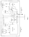
- FIG. 1 illustrates a memory module having built-in self test according to an embodiment of the present invention
- FIG. 2 illustrates a memory component having built-in self test according to an embodiment of the present invention.
- FIG. 1 illustrates a memory module having built-in self test (BIST) according to an embodiment of the present invention.
- BIST built-in self test
- the memory module 100 shown in FIG. 1 utilizes a set of buffers 130 , 140 , 150 in order to provide an interface with a processor component, such as a memory controller (not shown), which may be operating at a different voltage and/or frequency than the memory devices 110 , 120 , such as dynamic random access memory (DRAM) devices.
- a processor component such as a memory controller (not shown)
- DRAM dynamic random access memory
- a three-buffer configuration is utilized for the memory module 100 : two data buffers 1 st 130 , 2 nd 140 , and an address and command buffer 150 .
- the 1 st and 2 nd data buffers 130 , 140 and the address and command buffer 150 may be incorporated into a single buffer device, or additional buffer components may be utilized as well.
- the built-in self test (BIST) logic and circuitry are incorporated with the address and command buffer 150 .
- the address and command buffer preferably includes an address and command generator 154 to generate the address and commands and the test data to be transmitted to the memory devices 110 , 120 for testing.
- the BIST logic may utilize existing data extracted from the memory controller off of the data bus as the test data as well.
- the address and command generator 154 also generates compare test data, which is used to compare the test data read from the memory devices 110 , 120 , with the test data (which is identical to the compare test data) initially transmitted from the address/command generator 154 to the memory devices 110 , 120 for storage.
- the test data generated by the address/command generator 154 is transmitted to the memory devices 110 , 120 for storage therein. Then, the test data stored (written) in the memory devices 110 , 120 are read from the memory devices 110 , 120 and compared with the compare test data, which is identical to the test data, also generated by the address/command generator 154 .
- a comparator 145 such as an “exclusive OR” (XOR) comparator, may be provided in each one of the data buffers 130 , 140 to compare the test data read from the memory devices 110 , 120 with the compare test data provided by the address/command generator 154 .
- a determination of whether the comparison is a match or a failure is made by the comparator 145 , and a result then is preferably transmitted to a test result/status register 156 , that may be provided within the address and command buffer 150 .
- the test result/status register 156 may then provide a test status or result signal to an external device, such as a memory controller.
- the test status/result signal generated by the test result/status register 156 may utilize a two-bit packet, indicating, for example, the following states: BIST not enabled (00); BIST executing (01); BIST failed (10); and BIST passed (11).
- FIG. 1 illustrates a memory module 100 having two memory devices 110 , 120 , the memory module 100 is not limited to only two memory devices, and any suitable number may be used.
- the memory module 100 may use a slow speed clock signal, generating just one clock, and using a clock multiplier 152 within the address and command buffer 150 to multiply and distribute the clock signal to the memory devices 110 , 120 . Accordingly, by utilizing the memory module 100 illustrated in FIG. 1 , the memory module 100 may be tested independently of other systems, and expensive high-speed testers are not required to test the memory devices 110 , 120 and their connections within the memory module 100 itself.
- FIG. 2 illustrates a memory component having BIST according to an embodiment of the present invention.
- BIST logic may be provided completely within a single memory component, such as a buffer 210 and a memory device 220 . That is, each memory component may be taken independently of any other component and tested on its own.
- the buffer 210 may be an address and command buffer 150 , or a data buffer 130 , 140 , as discussed above with respect to FIG. 1 .
- the BIST logic includes a controller 260 to perform the BIST operations.
- the controller 260 preferably receives a clock signal, and also provides test result signals from the memory component, such as a buffer 210 or a memory device 220 .
- the controller 260 like the address and command generator 154 of FIG. 1 , is adapted to generate test data and compare test data to test the functional logic or memory array 250 (depending on the type of memory component, e.g., a buffer or memory device) of the buffer component 210 , or memory device 220 .
- the test data is preferably provided to the functional logic or memory array 250 , which is then transmitted to an input/output interface 230 , 240 .
- the test data may also be transmitted directly to the input/output interface 230 , 240 from the controller 260 to test the input/output interface 230 , 240 .
- the input/output interface 230 , 240 is configured with a loopback so that the test data may be directed back from an input/output connection to a compare register 270 to compare the test data from the input/output interface 230 , 240 , and ultimately, the functional logic or memory array 250 .
- the controller 260 is adapted to generate and provide compare test data to the compare register 270 so that the compare register 270 may compare the test data received from the input/output interface 230 , 240 with the compare test data to determine whether there was a match, and whether the test was successful. Accordingly, the compare register 270 makes a determination regarding the results of the test, and the test results are reported, preferably by the controller 260 .
- the compare register 270 and the controller 260 may be embodied within a single device or a common circuit.
- memory components such as a buffer 210 and a memory device 220 with BIST
- localized self-testing may be performed after the buffer 210 and the memory device 220 is manufactured.
- component-level built-in self test may be performed at various stages of manufacture and packaging, including at the wafer probe stage, during post-packaging, and even during post-assembly. Accordingly, the memory components 210 , 220 of FIG. 2 may be tested independently of other components, and expensive high-speed testers are not required to test the memory components 210 , 220 .
Abstract
A memory component with built-in self test includes a memory array. An input/output interface is coupled to the memory array and has a loopback. A controller is provided to transmit memory array test data to the memory array to store the memory array test data, and to read the memory array test data from the memory array. A compare register is also provided to compare the memory array test data transmitted to the memory array with the memory array test data read from the memory array.
Description
1. Field of the Invention
The present invention relates generally to memory systems, and more specifically, to memory modules and memory components, such as a memory device or a memory buffer, having built-in self test functionality.
2. Discussion of the Related Art
Integrated circuit devices such as random access memories (RAMs) usually undergo device verification testing during manufacture. Typically, such verification tests are designed to detect both static and dynamic defects in a memory array. Static defects include, for example, open circuit and short circuit defects in the integrated circuit device. Dynamic defects include defects such as weak pull-up or pull-down transistors that create timing sensitive defects.
A specialized integrated circuit device tester is normally employed to perform manufacturing verification tests. For example, such an integrated circuit device tester may be used to perform read/write verification cycle tests on the memory array. Relatively low-speed (e.g., 20 MHz), low-cost integrated circuit device testers are usually sufficient for detecting static defects in the memory array. However, extremely expensive integrated device testers are needed to detect dynamic defects in very high-speed memory arrays. Such expensive high-speed integrated circuit testers increase the overall manufacturing costs for such devices. In addition, for integrated circuit devices that include large memory arrays, the cycle time required to perform such read/write tests increases in proportion to the size of the array.
Attempts to overcome some of the difficulties associated with testing integrated circuit devices have included implementing built-in self-test (BIST) circuitry. For example, an integrated circuit cache memory array may contain circuitry to perform a standard static random access memory (SRAM) 13N March test algorithm on the memory array. A state machine is typically used to generate the 13N March test algorithm along with circuitry to sample data output and to generate a signature of the results. The signature is then compared against an expected value to determine whether defects exist in the memory array. Such BIST circuitry usually enables high-speed testing while obviating expensive high-speed testers.
Unfortunately, these BIST routines have generally only been able to apply a preprogrammed test sequence on the memory array. As the process of manufacturing such a memory array evolves, manufacturing test engineers typically develop improved strategies for detecting both static and dynamic defects in the memory array.
Moreover, such improved strategies for detecting defects can only be applied to testing that occurs while the device is placed in an expensive integrated circuit device tester. Therefore, engineers have been unable to achieve the benefits of improved test strategies without the use of an expensive tester, or without redesigning the integrated circuit device. Because of the advances in memory technology, and particularly in the area of narrow high-speed buses, which typically run at speeds of about 1.6 GHz, for use with dynamic random access memory devices (DRAMs), it is very expensive to obtain a high-speed tester capable of testing a memory module or a memory component at such high operating frequencies. Therefore, the added use of expensive high-speed hardware testers increases the time required to ascertain hardware failures, not to mention greatly increasing the overall manufacturing cost of these memory modules and memory components.
The memory module 100 shown in FIG. 1 utilizes a set of buffers 130, 140, 150 in order to provide an interface with a processor component, such as a memory controller (not shown), which may be operating at a different voltage and/or frequency than the memory devices 110, 120, such as dynamic random access memory (DRAM) devices. In the embodiment of FIG. 1 , a three-buffer configuration is utilized for the memory module 100: two data buffers 1st 130, 2nd 140, and an address and command buffer 150. However, the 1st and 2nd data buffers 130, 140 and the address and command buffer 150 may be incorporated into a single buffer device, or additional buffer components may be utilized as well.
In one embodiment, the built-in self test (BIST) logic and circuitry are incorporated with the address and command buffer 150. The address and command buffer preferably includes an address and command generator 154 to generate the address and commands and the test data to be transmitted to the memory devices 110, 120 for testing. However, instead of generating the test data, the BIST logic may utilize existing data extracted from the memory controller off of the data bus as the test data as well. Along with generating the test data, the address and command generator 154 also generates compare test data, which is used to compare the test data read from the memory devices 110, 120, with the test data (which is identical to the compare test data) initially transmitted from the address/command generator 154 to the memory devices 110,120 for storage.
In one embodiment, the test data generated by the address/command generator 154 is transmitted to the memory devices 110, 120 for storage therein. Then, the test data stored (written) in the memory devices 110, 120 are read from the memory devices 110, 120 and compared with the compare test data, which is identical to the test data, also generated by the address/command generator 154. A comparator 145, such as an “exclusive OR” (XOR) comparator, may be provided in each one of the data buffers 130,140 to compare the test data read from the memory devices 110, 120 with the compare test data provided by the address/command generator 154. A determination of whether the comparison is a match or a failure is made by the comparator 145, and a result then is preferably transmitted to a test result/status register 156, that may be provided within the address and command buffer 150. The test result/status register 156 may then provide a test status or result signal to an external device, such as a memory controller. The test status/result signal generated by the test result/status register 156 may utilize a two-bit packet, indicating, for example, the following states: BIST not enabled (00); BIST executing (01); BIST failed (10); and BIST passed (11). Although FIG. 1 illustrates a memory module 100 having two memory devices 110, 120, the memory module 100 is not limited to only two memory devices, and any suitable number may be used.
Additionally, rather than using a high-speed clock signal to perform testing, the memory module 100 may use a slow speed clock signal, generating just one clock, and using a clock multiplier 152 within the address and command buffer 150 to multiply and distribute the clock signal to the memory devices 110, 120. Accordingly, by utilizing the memory module 100 illustrated in FIG. 1 , the memory module 100 may be tested independently of other systems, and expensive high-speed testers are not required to test the memory devices 110,120 and their connections within the memory module 100 itself.
The BIST logic includes a controller 260 to perform the BIST operations. The controller 260 preferably receives a clock signal, and also provides test result signals from the memory component, such as a buffer 210 or a memory device 220. The controller 260, like the address and command generator 154 of FIG. 1 , is adapted to generate test data and compare test data to test the functional logic or memory array 250 (depending on the type of memory component, e.g., a buffer or memory device) of the buffer component 210, or memory device 220. The test data is preferably provided to the functional logic or memory array 250, which is then transmitted to an input/ output interface 230, 240. The test data may also be transmitted directly to the input/ output interface 230, 240 from the controller 260 to test the input/ output interface 230, 240.
The input/ output interface 230, 240 is configured with a loopback so that the test data may be directed back from an input/output connection to a compare register 270 to compare the test data from the input/ output interface 230, 240, and ultimately, the functional logic or memory array 250. The controller 260 is adapted to generate and provide compare test data to the compare register 270 so that the compare register 270 may compare the test data received from the input/ output interface 230, 240 with the compare test data to determine whether there was a match, and whether the test was successful. Accordingly, the compare register 270 makes a determination regarding the results of the test, and the test results are reported, preferably by the controller 260. The compare register 270 and the controller 260 may be embodied within a single device or a common circuit.
Therefore, by having memory components such as a buffer 210 and a memory device 220 with BIST, localized self-testing may be performed after the buffer 210 and the memory device 220 is manufactured. However, component-level built-in self test may be performed at various stages of manufacture and packaging, including at the wafer probe stage, during post-packaging, and even during post-assembly. Accordingly, the memory components 210, 220 of FIG. 2 may be tested independently of other components, and expensive high-speed testers are not required to test the memory components 210, 220.
While the description above refers to particular embodiments of the present invention, it will be understood that many modifications may be made without departing from the spirit thereof. The accompanying claims are intended to cover such modifications as would fall within the true scope and spirit of the present invention. The presently disclosed embodiments are therefore to be considered in all respects as illustrative and not restrictive, the scope of the invention being indicated by the appended claims, rather than the foregoing description, and all changes that come within the meaning and range of equivalency of the claims are therefore intended to be embraced therein.
Claims (64)
1. A memory component with built-in self test, comprising:
an input/output interface having a loopback;
a controller to transmit input/output test data to the input/output interface, and to receive the input/output test data from the loopback of the input/output interface; and
a compare register to store and compare the input/output test data transmitted to the input/output interface with the input/output test data received from the input/output interface, wherein the memory component resides within a memory module having a plurality of memory devices and at least one buffer.
2. The memory component according to claim 1 , wherein the memory component is a dynamic random access memory (DRAM).
3. The memory component according to claim 1 , wherein the memory component is a buffer.
4. The memory component according to claim 3 , wherein the buffer is an address and command buffer.
5. The memory component according to claim 3 , wherein the buffer is a data buffer.
6. The memory component according to claim 3 , wherein the buffer is an address and command and data buffer.
7. The memory component according to claim 1 , wherein the compare register generates a test result based on the input/output test data transmitted to the input/output interface compared with the input/output test data received from the input/output interface.
8. The memory component according to claim 1 , wherein the controller is adapted to transmit memory array test data to a memory array to store the test data therein, and to read the memory array test data from the memory array, and the compare register is adapted to compare the memory array test data transmitted to the memory array with the memory array test data read from the memory array.
9. A memory component with built-in self test, comprising:
a memory array;
an input/output interface coupled to the memory array and having a loopback;
a controller to transmit memory array test data to the memory array to store the memory array test data, and to read the memory array test data from the memory array; and
a compare register to store and compare the memory array test data transmitted to the memory array with the memory array test data read from the memory array, wherein the memory component resides within a memory module having a plurality of memory devices and at least one buffer.
10. The memory component according to claim 9 , wherein the memory component is a dynamic random access memory (DRAM).
11. The memory component according to claim 9 , wherein the memory component is a buffer.
12. The memory component according to claim 11 , wherein the buffer is an address and command buffer.
13. The memory component according to claim 11 , wherein the buffer is a data buffer.
14. The memory component according to claim 11 , wherein the buffer is an address and command and data buffer.
15. The memory component according to claim 9 , wherein the compare register generates a test result based on the memory array test data transmitted to the memory array compared with the memory array test data read from the memory array.
16. A method of testing a memory component with built-in self test, comprising:
transmitting input/output test data to an input/output interface having a loopback;
receiving the input/output test data from the loopback of the input/output interface;
storing the input/output test data transmitted to the input/output interface and the input/output test data received from the input/output interface in a register; and
comparing the input/output test data transmitted to the input/output interface with the input/output test data received from the input/output interface, wherein the memory component resides within a memory module having a plurality of memory devices and at least one buffer.
17. The method according to claim 16 , wherein the memory component is a dynamic random access memory (DRAM).
18. The method according to claim 16 , wherein the memory component is a buffer.
19. The method according to claim 18 , wherein the buffer is an address and command buffer.
20. The method according to claim 18 , wherein the buffer is a data buffer.
21. The method according to claim 18 , wherein the buffer is an address and command and data buffer.
22. The method according to claim 18 , wherein the buffer is an address and command buffer.
23. The method according to claim 18 , wherein the buffer is a data buffer.
24. The method according to claim 18 , wherein the buffer is an address and command and data buffer.
25. The method according to claim 16 , wherein the compare register generates a test result based on the input/output test data transmitted to the input/output interface compared with the input/output test data received from the input/output interface.
26. The method according to claim 16 , further including:
transmitting memory array test data to a memory array;
storing the memory array test data in the memory array;
reading the memory array test data from the memory array; and
comparing the memory array test data transmitted to the memory array with the memory array test data read from the memory array.
27. The method according to claim 24 , wherein the memory component is a dynamic random access memory (DRAM).
28. The method according to claim 24 , wherein the memory component is a buffer.
29. A method of testing a memory component with built-in self test, comprising:
transmitting memory array test data to a memory array;
storing the memory array test data in the memory array;
reading the memory array test data from the memory array;
storing the memory array test data transmitted to the memory array and the memory array test data read from the memory array in a register; and
comparing the memory array test data transmitted to the memory array with the memory array test data read from the memory array, wherein the memory component resides within a memory module having a plurality of memory devices and at least one buffer.
30. The method according to claim 29 , wherein the memory component is a dynamic random access memory (DRAM).
31. The method according to claim 29 , wherein the memory component is a buffer.
32. The method according to claim 31 , wherein the buffer is an address and command buffer.
33. The method according to claim 31 , wherein the buffer is a data buffer.
34. The method according to claim 31 , wherein the buffer is an address and command and data buffer.
35. The method according to claim 29 , wherein the compare register generates a test result based on the memory array test data transmitted to the memory array compared with the memory array test data read from the memory array.
36. A memory module with built-in self test, comprising:
a plurality of memory components;
an address and command buffer adapted to transmit address and command data and test data to one of the plurality of memory components, wherein the address and command buffer includes a register to receive a test result; and
at least one data buffer to receive the test data from the address and command buffer, to receive the test data from the one of the plurality of memory components, and to compare the test data received from the address and command buffer with the test data received from the one of the plurality of memory components to generate the test result, wherein the plurality of memory components, the address and command buffer, and the at least one data buffer all reside within the memory module.
37. The memory module according to claim 36 , wherein the address and command buffer and the data buffer are within a single buffer chip.
38. The memory module according to claim 36 , wherein the at least one memory component is a dynamic random access memory (DRAM).
39. The memory module according to claim 36 , wherein the address and command buffer includes a clock multiplier to receive a clock signal and to multiply the clock signal for transmission to the at least one memory component and the at least one data buffer.
40. The memory module according to claim 36 , wherein the address and command buffer includes an address and command generator to generate the address and command data.
41. The memory module according to claim 36 , wherein the test data is obtained from a data bus through a memory controller.
42. The memory module according to claim 36 , wherein the register receives the test result from the at least one data buffer and reports the test result as one of the following conditions: built-in self test not enabled, built-in self test enabled, built-in self test failed, and built-in self test passed.
43. The memory module according to claim 36 , wherein the at least one data buffer utilizes an exclusive-OR (XOR) comparator to compare the test data received from the address and command buffer with the test data received from the at least one memory component.
44. A method of testing a memory module with built-in self test, the method comprising:
transmitting address and command data and test data to a memory component among a plurality of memory components from an address and command buffer, wherein the plurality of memory components and the address and command buffer all reside within the memory module;
receiving the test data from the address and command buffer;
receiving the test data from the memory component; and
comparing the test data received from the address and command buffer with the test data received from the memory component to generate a test result.
45. The method according to claim 44 , wherein receiving the test data from the address and command buffer, receiving the test data from the memory component, and comparing the test data are performed in a data buffer.
46. The method according to claim 45 , wherein the data buffer and the address and command buffer are within a single buffer chip.
47. The method according to claim 44 , wherein the memory component is a dynamic random access memory (DRAM).
48. The method according to claim 44 , further including:
receiving a clock signal by a clock multiplier of the address and command buffer;
multiplying the clock signal; and
transmitting the clock signal to the memory component and a data buffer.
49. The method according to claim 44 , further including:
generating the address and command data from an address and command data generator of the address and command buffer.
50. The method according to claim 44 , further including:
obtaining the test data from a data bus through a memory controller.
51. The method according to claim 44 , further including:
receiving the test result in a register of the address and command buffer; and
reporting the test result from the register as one of the following conditions: built-in self test not enabled, built-in self test enabled, built-in self test failed, and built-in self test passed.
52. The method according to claim 44 , wherein comparing the test data received from the address and command buffer with the test data received from the memory component is performed by a data buffer utilizing an exclusive-OR (XOR) comparator.
53. A memory module with built-in self test, comprising:
a plurality of memory components;
an address and command buffer adapted to transmit address and command data and test data to one of the plurality of memory components, wherein the address and command buffer includes,
a register to receive a test result,
a clock multiplier to receive a clock signal and to multiply the clock signal for transmission, and
an address and command generator to generate the address and command data; and
at least one data buffer to receive the test data from the address and command buffer, to receive the test data from the one of the plurality of memory components, and to compare the test data received from the address and command buffer with the test data received from the one of the plurality of memory components to generate the test result, wherein the plurality of memory components, the address and command buffer, and the at least one data buffer all reside within the memory module.
54. The memory module according to claim 53 , wherein the address and command buffer and the data buffer are within a single buffer chip.
55. The memory module according to claim 53 , wherein the at least one memory component is a dynamic random access memory (DRAM).
56. The memory module according to claim 53 , wherein the test data is obtained from a data bus through a memory controller.
57. The memory module according to claim 53 , wherein the register receives the test result from the at least one data buffer and reports the test result as one of the following conditions: built-in self test not enabled, built-in self test enabled, built-in self test failed, and built-in self test passed.
58. The memory module according to claim 53 , wherein the at least one data buffer utilizes an exclusive-OR (XOR) comparator to compare the test data received from the address and command buffer with the test data received from the at least one memory component.
59. A memory component with built-in self test, comprising:
a memory array;
an input/output interface coupled to the memory array and having a loopback;
a controller to transmit memory array and test data to the memory array to store the memory array test data, to read the memory array test data from the memory array, to receive the memory array test data from the loopback of the input/output interface that was transmitted by the memory array to the input/output interface, to transmit input/output test data to the input/output interface, and to receive the input/output test data from the loopback of the input/output interface; and
a compare register to store and compare the memory array test data transmitted to the memory array with the memory array test data read from the memory array, to store and compare the memory array test data transmitted to the memory array with the memory array test data received from the loopback of the input/output interface that was transmitted from the memory array, and to store and compare the input/output test data transmitted to the input/output interface with the input/output test data received from the loopback of the input/output interface, wherein the compare register generates a test result based on the memory array test data transmitted to the memory array compared with the memory array test data read from the memory array, generates a test result based on the memory array test data transmitted to the memory array compared with the memory array test data received from the loopback of the input/output interface that was transmitted by the memory array to the input/output interface, and generates a test result based on the input/output test data transmitted to the input/output interface compared with the input/output test data received from the loopback of the input/output interface.
60. The memory component according to claim 59 , wherein the memory component is a dynamic random access memory (DRAM).
61. The memory component according to claim 59 , wherein the memory component is a buffer.
62. The memory component according to claim 61 , wherein the buffer is an address and command buffer.
63. The memory component according to claim 61 , wherein the buffer is a data buffer.
64. A method of testing a memory component with built-in self test, comprising:
transmitting memory array test data to a memory array to store the memory array test data;
reading the memory array test data from the memory array;
receiving the memory array test data from a loopback of an input/output interface that was transmitted by the memory array to the input/output interface;
transmitting input/output test data to the input/output interface;
receiving the input/output test data from the loopback of the input/output interface;
storing and comparing the memory array test data transmitted to the memory array with the memory array test data read from the memory array;
storing and comparing the memory array test data transmitted to the memory array with the memory array test data received from the loopback of the input/output interface that was transmitted from the memory array;
storing and comparing the input/output test data transmitted to the input/output interface with the input/output test data received from the loopback of the input/output interface;
generating a test result based on the memory array test data transmitted to the memory array compared with the memory array test data read from the memory array;
generating a test result based on the memory array test data transmitted to the memory array compared with the memory array test data received from the loopback of the input/output interface that was transmitted by the memory array to the input/output interface; and
generating a test result based on the input/output test data transmitted to the input/output interface compared with the input/output test data received from the loopback of the input/output interface.
Priority Applications (7)
| Application Number | Priority Date | Filing Date | Title |
|---|---|---|---|
| US09/664,910 US6928593B1 (en) | 2000-09-18 | 2000-09-18 | Memory module and memory component built-in self test |
| DE10196635T DE10196635B4 (en) | 2000-09-18 | 2001-09-14 | Memory module and built-in memory component self-test |
| CNB018189849A CN1319072C (en) | 2000-09-18 | 2001-09-14 | Memory module and memory component with built-in self test function |
| PCT/US2001/028774 WO2002025957A2 (en) | 2000-09-18 | 2001-09-14 | Memory module and memory component built-in self test |
| AU2001290935A AU2001290935A1 (en) | 2000-09-18 | 2001-09-14 | Memory module and memory component built-in self test |
| TW090123025A TWI234784B (en) | 2000-09-18 | 2001-09-19 | Memory module and memory component built-in self test |
| HK04105978A HK1063264A1 (en) | 2000-09-18 | 2004-08-10 | Memory module and memory component built-in self test and methods thereof |
Applications Claiming Priority (1)
| Application Number | Priority Date | Filing Date | Title |
|---|---|---|---|
| US09/664,910 US6928593B1 (en) | 2000-09-18 | 2000-09-18 | Memory module and memory component built-in self test |
Publications (1)
| Publication Number | Publication Date |
|---|---|
| US6928593B1 true US6928593B1 (en) | 2005-08-09 |
Family
ID=24667948
Family Applications (1)
| Application Number | Title | Priority Date | Filing Date |
|---|---|---|---|
| US09/664,910 Expired - Lifetime US6928593B1 (en) | 2000-09-18 | 2000-09-18 | Memory module and memory component built-in self test |
Country Status (7)
| Country | Link |
|---|---|
| US (1) | US6928593B1 (en) |
| CN (1) | CN1319072C (en) |
| AU (1) | AU2001290935A1 (en) |
| DE (1) | DE10196635B4 (en) |
| HK (1) | HK1063264A1 (en) |
| TW (1) | TWI234784B (en) |
| WO (1) | WO2002025957A2 (en) |
Cited By (16)
| Publication number | Priority date | Publication date | Assignee | Title |
|---|---|---|---|---|
| US20040145935A1 (en) * | 2002-12-20 | 2004-07-29 | Andreas Jakobs | Memory module with a test device |
| US20040267479A1 (en) * | 2003-06-30 | 2004-12-30 | Bruce Querbach | Automatic self test of an integrated circuit component via AC I/O loopback |
| US20050193253A1 (en) * | 2004-02-13 | 2005-09-01 | International Business Machines Corporation | A Command Multiplier for Built-In-Self-Test |
| US20080307276A1 (en) * | 2007-06-08 | 2008-12-11 | Luka Bodrozic | Memory Controller with Loopback Test Interface |
| US20090055698A1 (en) * | 2007-08-21 | 2009-02-26 | Micron Technology, Inc. | System, apparatus, and method for memory built-in self testing using microcode sequencers |
| US20110004793A1 (en) * | 2009-07-02 | 2011-01-06 | Chinsong Sul | Computer memory test structure |
| US20110158016A1 (en) * | 2009-12-30 | 2011-06-30 | Stmicroelectronics S.R.I. | Integrated solution for identifying malfunctioning components within memory devices |
| US20110167308A1 (en) * | 2010-01-06 | 2011-07-07 | Chinsong Sul | Multi-site testing of computer memory devices and serial io ports |
| US20110188386A1 (en) * | 2010-02-02 | 2011-08-04 | Juniper Networks Inc. | Packet-based memory test of a network device |
| US8001434B1 (en) | 2008-04-14 | 2011-08-16 | Netlist, Inc. | Memory board with self-testing capability |
| US8154901B1 (en) | 2008-04-14 | 2012-04-10 | Netlist, Inc. | Circuit providing load isolation and noise reduction |
| US20130173966A1 (en) * | 2010-07-23 | 2013-07-04 | Panasonic Corporation | Memory controller and memory access system |
| US9299400B2 (en) | 2012-09-28 | 2016-03-29 | Intel Corporation | Distributed row hammer tracking |
| US9548137B2 (en) | 2013-12-26 | 2017-01-17 | Intel Corporation | Integrated circuit defect detection and repair |
| US9564245B2 (en) | 2013-12-26 | 2017-02-07 | Intel Corporation | Integrated circuit defect detection and repair |
| US9959185B2 (en) * | 2016-04-28 | 2018-05-01 | United Microelectronics Corp. | Memory system capable of generating notification signals |
Families Citing this family (14)
| Publication number | Priority date | Publication date | Assignee | Title |
|---|---|---|---|---|
| DE10300781B4 (en) * | 2003-01-11 | 2014-02-06 | Qimonda Ag | Memory module, test system and method for testing one or more memory modules |
| DE10317371A1 (en) * | 2003-04-15 | 2004-11-11 | Infineon Technologies Ag | Data interface circuit for data exchange between integrated circuit and external circuit with data protocol unit preparing exchangeable data, with test data buffer, transmitting stored data in test mode to protocol unit |
| US7184916B2 (en) * | 2003-05-20 | 2007-02-27 | Cray Inc. | Apparatus and method for testing memory cards |
| US20050289287A1 (en) * | 2004-06-11 | 2005-12-29 | Seung-Man Shin | Method and apparatus for interfacing between test system and embedded memory on test mode setting operation |
| DE102004043051A1 (en) * | 2004-09-06 | 2006-03-30 | Infineon Technologies Ag | Loop-back method for measuring the interface timing of semiconductor memory devices using the normal-mode memory |
| KR100770749B1 (en) * | 2006-07-11 | 2007-10-26 | 삼성전자주식회사 | Memory controller adding a self test function and methods using the same |
| EP1927949A1 (en) * | 2006-12-01 | 2008-06-04 | Thomson Licensing | Array of processing elements with local registers |
| CN102013274B (en) * | 2010-11-10 | 2013-08-07 | 无锡中星微电子有限公司 | Self-test circuit and method for storage |
| CN103198001B (en) * | 2013-04-25 | 2017-02-01 | 加弘科技咨询(上海)有限公司 | Storage system capable of self-testing peripheral component interface express (PCIE) interface and test method |
| CN104425040A (en) * | 2013-08-23 | 2015-03-18 | 辉达公司 | Memory testing method and system thereof |
| CN103943152B (en) * | 2014-03-31 | 2017-02-01 | 西安紫光国芯半导体有限公司 | Rapid built-in self-testing system and method of memory |
| CN105070321B (en) * | 2015-08-18 | 2019-03-08 | 珠海市一微半导体有限公司 | The quick test circuit and method of memory device |
| CN107305789B (en) * | 2016-04-21 | 2020-08-07 | 北京兆易创新科技股份有限公司 | Self-testing method and device of non-volatile memory |
| TWI776785B (en) * | 2022-04-07 | 2022-09-01 | 點序科技股份有限公司 | Die test system and die test method thereof |
Citations (19)
| Publication number | Priority date | Publication date | Assignee | Title |
|---|---|---|---|---|
| US4837785A (en) * | 1983-06-14 | 1989-06-06 | Aptec Computer Systems, Inc. | Data transfer system and method of operation thereof |
| USRE34445E (en) | 1985-01-18 | 1993-11-16 | University Of Michigan | Self-testing dynamic RAM |
| US5613153A (en) | 1994-10-03 | 1997-03-18 | International Business Machines Corporation | Coherency and synchronization mechanisms for I/O channel controllers in a data processing system |
| US5633878A (en) * | 1995-01-20 | 1997-05-27 | Telefonaktiebolaget Lm Ericsson | Self-diagnostic data buffers |
| US5638382A (en) * | 1994-06-29 | 1997-06-10 | Intel Corporation | Built-in self test function for a processor including intermediate test results |
| US5748640A (en) | 1996-09-12 | 1998-05-05 | Advanced Micro Devices | Technique for incorporating a built-in self-test (BIST) of a DRAM block with existing functional test vectors for a microprocessor |
| US5815427A (en) * | 1997-04-02 | 1998-09-29 | Micron Technology, Inc. | Modular memory circuit and method for forming same |
| US5835936A (en) * | 1995-07-06 | 1998-11-10 | Mitsubishi Electric Corp | Single-chip flash-memory device using serial command, address, and data communcations |
| US5883843A (en) * | 1996-04-30 | 1999-03-16 | Texas Instruments Incorporated | Built-in self-test arrangement for integrated circuit memory devices |
| US5946247A (en) * | 1994-05-26 | 1999-08-31 | Mitsubishi Denki Kabushiki Kaisha | Semiconductor memory testing device |
| US5961653A (en) | 1997-02-19 | 1999-10-05 | International Business Machines Corporation | Processor based BIST for an embedded memory |
| US5982681A (en) | 1997-10-10 | 1999-11-09 | Lsi Logic Corporation | Reconfigurable built-in self test circuit |
| US6019501A (en) * | 1991-03-29 | 2000-02-01 | Advantest Corporation | Address generating device for memory tester |
| US6058056A (en) * | 1998-04-30 | 2000-05-02 | Micron Technology, Inc. | Data compression circuit and method for testing memory devices |
| US6182257B1 (en) | 1997-07-31 | 2001-01-30 | Mosaid Technologies Incorporated | BIST memory test system |
| US6247070B1 (en) * | 1997-07-01 | 2001-06-12 | Micron Technology, Inc. | Pipelined packet-oriented memory system having a undirectional command and address bus and a bidirectional data bus |
| US20010014925A1 (en) | 2000-02-10 | 2001-08-16 | Ichiro Kumata | Bus emulation apparatus |
| US6415403B1 (en) * | 1999-01-29 | 2002-07-02 | Global Unichip Corporation | Programmable built in self test for embedded DRAM |
| US6477674B1 (en) * | 1999-12-29 | 2002-11-05 | Intel Corporation | Method and apparatus for conducting input/output loop back tests using a local pattern generator and delay elements |
Family Cites Families (3)
| Publication number | Priority date | Publication date | Assignee | Title |
|---|---|---|---|---|
| JPH0553924A (en) * | 1991-08-26 | 1993-03-05 | Nec Corp | System for testing storage device |
| EP0744755A1 (en) * | 1995-05-25 | 1996-11-27 | International Business Machines Corporation | Test method and device for embedded memories on semiconductor substrates |
| US5982684A (en) * | 1998-05-28 | 1999-11-09 | Intel Corporation | Parallel access testing of a memory array |
-
2000
- 2000-09-18 US US09/664,910 patent/US6928593B1/en not_active Expired - Lifetime
-
2001
- 2001-09-14 AU AU2001290935A patent/AU2001290935A1/en not_active Abandoned
- 2001-09-14 WO PCT/US2001/028774 patent/WO2002025957A2/en active Application Filing
- 2001-09-14 CN CNB018189849A patent/CN1319072C/en not_active Expired - Fee Related
- 2001-09-14 DE DE10196635T patent/DE10196635B4/en not_active Expired - Fee Related
- 2001-09-19 TW TW090123025A patent/TWI234784B/en not_active IP Right Cessation
-
2004
- 2004-08-10 HK HK04105978A patent/HK1063264A1/en not_active IP Right Cessation
Patent Citations (19)
| Publication number | Priority date | Publication date | Assignee | Title |
|---|---|---|---|---|
| US4837785A (en) * | 1983-06-14 | 1989-06-06 | Aptec Computer Systems, Inc. | Data transfer system and method of operation thereof |
| USRE34445E (en) | 1985-01-18 | 1993-11-16 | University Of Michigan | Self-testing dynamic RAM |
| US6019501A (en) * | 1991-03-29 | 2000-02-01 | Advantest Corporation | Address generating device for memory tester |
| US5946247A (en) * | 1994-05-26 | 1999-08-31 | Mitsubishi Denki Kabushiki Kaisha | Semiconductor memory testing device |
| US5638382A (en) * | 1994-06-29 | 1997-06-10 | Intel Corporation | Built-in self test function for a processor including intermediate test results |
| US5613153A (en) | 1994-10-03 | 1997-03-18 | International Business Machines Corporation | Coherency and synchronization mechanisms for I/O channel controllers in a data processing system |
| US5633878A (en) * | 1995-01-20 | 1997-05-27 | Telefonaktiebolaget Lm Ericsson | Self-diagnostic data buffers |
| US5835936A (en) * | 1995-07-06 | 1998-11-10 | Mitsubishi Electric Corp | Single-chip flash-memory device using serial command, address, and data communcations |
| US5883843A (en) * | 1996-04-30 | 1999-03-16 | Texas Instruments Incorporated | Built-in self-test arrangement for integrated circuit memory devices |
| US5748640A (en) | 1996-09-12 | 1998-05-05 | Advanced Micro Devices | Technique for incorporating a built-in self-test (BIST) of a DRAM block with existing functional test vectors for a microprocessor |
| US5961653A (en) | 1997-02-19 | 1999-10-05 | International Business Machines Corporation | Processor based BIST for an embedded memory |
| US5815427A (en) * | 1997-04-02 | 1998-09-29 | Micron Technology, Inc. | Modular memory circuit and method for forming same |
| US6247070B1 (en) * | 1997-07-01 | 2001-06-12 | Micron Technology, Inc. | Pipelined packet-oriented memory system having a undirectional command and address bus and a bidirectional data bus |
| US6182257B1 (en) | 1997-07-31 | 2001-01-30 | Mosaid Technologies Incorporated | BIST memory test system |
| US5982681A (en) | 1997-10-10 | 1999-11-09 | Lsi Logic Corporation | Reconfigurable built-in self test circuit |
| US6058056A (en) * | 1998-04-30 | 2000-05-02 | Micron Technology, Inc. | Data compression circuit and method for testing memory devices |
| US6415403B1 (en) * | 1999-01-29 | 2002-07-02 | Global Unichip Corporation | Programmable built in self test for embedded DRAM |
| US6477674B1 (en) * | 1999-12-29 | 2002-11-05 | Intel Corporation | Method and apparatus for conducting input/output loop back tests using a local pattern generator and delay elements |
| US20010014925A1 (en) | 2000-02-10 | 2001-08-16 | Ichiro Kumata | Bus emulation apparatus |
Non-Patent Citations (1)
| Title |
|---|
| A 72K CMOS Channelless Gate Array with Embedded 1Mbit Dynamic RAM, Kazuhiro Sawada, et al., pp. 20.3.1-20.3.4. |
Cited By (44)
| Publication number | Priority date | Publication date | Assignee | Title |
|---|---|---|---|---|
| US20040145935A1 (en) * | 2002-12-20 | 2004-07-29 | Andreas Jakobs | Memory module with a test device |
| US7315969B2 (en) * | 2002-12-20 | 2008-01-01 | Infineon Technologies Ag | Memory module with a test device |
| US20040267479A1 (en) * | 2003-06-30 | 2004-12-30 | Bruce Querbach | Automatic self test of an integrated circuit component via AC I/O loopback |
| US7139957B2 (en) * | 2003-06-30 | 2006-11-21 | Intel Corporation | Automatic self test of an integrated circuit component via AC I/O loopback |
| US20050193253A1 (en) * | 2004-02-13 | 2005-09-01 | International Business Machines Corporation | A Command Multiplier for Built-In-Self-Test |
| US7194670B2 (en) * | 2004-02-13 | 2007-03-20 | International Business Machines Corp. | Command multiplier for built-in-self-test |
| US7836372B2 (en) | 2007-06-08 | 2010-11-16 | Apple Inc. | Memory controller with loopback test interface |
| US20110035560A1 (en) * | 2007-06-08 | 2011-02-10 | Luka Bodrozic | Memory Controller with Loopback Test Interface |
| US8086915B2 (en) | 2007-06-08 | 2011-12-27 | Apple Inc. | Memory controller with loopback test interface |
| US20080307276A1 (en) * | 2007-06-08 | 2008-12-11 | Luka Bodrozic | Memory Controller with Loopback Test Interface |
| US8301941B2 (en) | 2007-06-08 | 2012-10-30 | Apple Inc. | Memory controller with loopback test interface |
| US20100223512A1 (en) * | 2007-08-21 | 2010-09-02 | Micron Technology, Inc. | System, apparatus, and method for memory built in self testing using microcode sequencers |
| US20090055698A1 (en) * | 2007-08-21 | 2009-02-26 | Micron Technology, Inc. | System, apparatus, and method for memory built-in self testing using microcode sequencers |
| US7954029B2 (en) | 2007-08-21 | 2011-05-31 | Micron Technology, Inc. | System, apparatus, and method for memory built-in self testing using microcode sequencers |
| US7721175B2 (en) | 2007-08-21 | 2010-05-18 | Micron Technology, Inc. | System, apparatus, and method for memory built-in self testing using microcode sequencers |
| US11862267B2 (en) | 2008-04-14 | 2024-01-02 | Netlist, Inc. | Multi mode memory module with data handlers |
| US10217523B1 (en) | 2008-04-14 | 2019-02-26 | Netlist, Inc. | Multi-mode memory module with data handlers |
| US8782350B2 (en) | 2008-04-14 | 2014-07-15 | Netlist, Inc. | Circuit providing load isolation and noise reduction |
| US8359501B1 (en) | 2008-04-14 | 2013-01-22 | Netlist, Inc. | Memory board with self-testing capability |
| US8001434B1 (en) | 2008-04-14 | 2011-08-16 | Netlist, Inc. | Memory board with self-testing capability |
| US8154901B1 (en) | 2008-04-14 | 2012-04-10 | Netlist, Inc. | Circuit providing load isolation and noise reduction |
| US20110004793A1 (en) * | 2009-07-02 | 2011-01-06 | Chinsong Sul | Computer memory test structure |
| US8667354B2 (en) | 2009-07-02 | 2014-03-04 | Silicon Image, Inc. | Computer memory test structure |
| WO2011002621A1 (en) | 2009-07-02 | 2011-01-06 | Silicon Image, Inc. | Computer memory test structure |
| US8386867B2 (en) | 2009-07-02 | 2013-02-26 | Silicon Image, Inc. | Computer memory test structure |
| KR20120095842A (en) * | 2009-07-02 | 2012-08-29 | 실리콘 이미지, 인크. | Computer memory test structure |
| KR101714630B1 (en) | 2009-07-02 | 2017-03-09 | 래티스세미컨덕터코퍼레이션 | Computer memory test structure |
| US8924805B2 (en) | 2009-07-02 | 2014-12-30 | Silicon Image, Inc. | Computer memory test structure |
| US8320207B2 (en) * | 2009-12-30 | 2012-11-27 | Stmicroelectronics S.R.L. | Integrated solution for identifying malfunctioning components within memory devices |
| US20110158016A1 (en) * | 2009-12-30 | 2011-06-30 | Stmicroelectronics S.R.I. | Integrated solution for identifying malfunctioning components within memory devices |
| US8588018B2 (en) | 2009-12-30 | 2013-11-19 | Stmicroelectronics S.R.L. | Integrated solution for identifying malfunctioning components within memory devices |
| WO2011084928A3 (en) * | 2010-01-06 | 2013-07-04 | Silicon Image, Inc. | Multi-site testing of computer memory devices and serial io ports |
| US20110167308A1 (en) * | 2010-01-06 | 2011-07-07 | Chinsong Sul | Multi-site testing of computer memory devices and serial io ports |
| US8839058B2 (en) | 2010-01-06 | 2014-09-16 | Silicon Image, Inc. | Multi-site testing of computer memory devices and serial IO ports |
| US8543873B2 (en) | 2010-01-06 | 2013-09-24 | Silicon Image, Inc. | Multi-site testing of computer memory devices and serial IO ports |
| US20110188386A1 (en) * | 2010-02-02 | 2011-08-04 | Juniper Networks Inc. | Packet-based memory test of a network device |
| US8345558B2 (en) * | 2010-02-02 | 2013-01-01 | Juniper Networks, Inc. | Packet-based memory test of a network device |
| US20130173966A1 (en) * | 2010-07-23 | 2013-07-04 | Panasonic Corporation | Memory controller and memory access system |
| US8972790B2 (en) * | 2010-07-23 | 2015-03-03 | Panasonic Intellectual Property Management Co., Ltd. | Memory controller and memory access system with error detection using data comparison of loop-backed signals |
| US9299400B2 (en) | 2012-09-28 | 2016-03-29 | Intel Corporation | Distributed row hammer tracking |
| US9564245B2 (en) | 2013-12-26 | 2017-02-07 | Intel Corporation | Integrated circuit defect detection and repair |
| US9548137B2 (en) | 2013-12-26 | 2017-01-17 | Intel Corporation | Integrated circuit defect detection and repair |
| US9922725B2 (en) | 2013-12-26 | 2018-03-20 | Intel Corporation | Integrated circuit defect detection and repair |
| US9959185B2 (en) * | 2016-04-28 | 2018-05-01 | United Microelectronics Corp. | Memory system capable of generating notification signals |
Also Published As
| Publication number | Publication date |
|---|---|
| CN1475015A (en) | 2004-02-11 |
| DE10196635T1 (en) | 2003-08-21 |
| WO2002025957A2 (en) | 2002-03-28 |
| WO2002025957A3 (en) | 2002-07-11 |
| AU2001290935A1 (en) | 2002-04-02 |
| HK1063264A1 (en) | 2004-12-17 |
| CN1319072C (en) | 2007-05-30 |
| TWI234784B (en) | 2005-06-21 |
| DE10196635B4 (en) | 2011-06-16 |
Similar Documents
| Publication | Publication Date | Title |
|---|---|---|
| US6928593B1 (en) | Memory module and memory component built-in self test | |
| KR100234504B1 (en) | Method and built-in self-test apparatus for testing an integrated circuit which capture failure information for a selected failure | |
| US6658611B1 (en) | Programmable built-in self-test system for semiconductor memory device | |
| JP4571749B2 (en) | Efficient simultaneous testing of integrated circuit devices to produce expected responses using known good devices | |
| US6617842B2 (en) | Semiconductor device testing method and system employing trace data | |
| US7114113B2 (en) | Test circuit provided with built-in self test function | |
| US6424583B1 (en) | System and measuring access time of embedded memories | |
| KR100679586B1 (en) | Integrated circuit memory device having built-in self test circuit with monitor and tester modes | |
| JPH06295599A (en) | Semiconductor memory device | |
| US20100027354A1 (en) | Semiconductor memory device and method for testing same | |
| US7539912B2 (en) | Method and apparatus for testing a fully buffered memory module | |
| US20080082883A1 (en) | System for and method of performing high speed memory diagnostics via built-in-self-test | |
| US6226764B1 (en) | Integrated circuit memory devices including internal stress voltage generating circuits and methods for built-in self test (BIST) | |
| US20030210069A1 (en) | Semiconductor device, and the method of testing or making of the semiconductor device | |
| US5777932A (en) | Semiconductor memory device test circuit having an improved compare signal generator circuit | |
| US6671836B1 (en) | Method and apparatus for testing memory | |
| US7096386B2 (en) | Semiconductor integrated circuit having functional modules each including a built-in self testing circuit | |
| US10650908B2 (en) | Semiconductor device and system including the same | |
| US7490279B1 (en) | Test interface for random access memory (RAM) built-in self-test (BIST) | |
| US20030120989A1 (en) | Method and circuit to implement double data rate testing | |
| CN115691632B (en) | Test control system and method | |
| KR102538991B1 (en) | Semiconductor test device and semiconductor test method | |
| US6115303A (en) | Method and apparatus for testing memory devices | |
| US20030033557A1 (en) | Semiconductor memory testing device | |
| CN114333959A (en) | Memory self-checking device and method |
Legal Events
| Date | Code | Title | Description |
|---|---|---|---|
| AS | Assignment |
Owner name: INTEL CORPORATION, CALIFORNIA Free format text: ASSIGNMENT OF ASSIGNORS INTEREST;ASSIGNORS:HALBERT, JOHN;BONELLA, RANDY M.;REEL/FRAME:011851/0293;SIGNING DATES FROM 20001214 TO 20010105 |
|
| STCF | Information on status: patent grant |
Free format text: PATENTED CASE |
|
| FPAY | Fee payment |
Year of fee payment: 4 |
|
| FPAY | Fee payment |
Year of fee payment: 8 |
|
| SULP | Surcharge for late payment |
Year of fee payment: 7 |
|
| FPAY | Fee payment |
Year of fee payment: 12 |