US6930357B2 - Active SOI structure with a body contact through an insulator - Google Patents
Active SOI structure with a body contact through an insulator Download PDFInfo
- Publication number
- US6930357B2 US6930357B2 US10/463,023 US46302303A US6930357B2 US 6930357 B2 US6930357 B2 US 6930357B2 US 46302303 A US46302303 A US 46302303A US 6930357 B2 US6930357 B2 US 6930357B2
- Authority
- US
- United States
- Prior art keywords
- silicon
- insulator
- oxide layer
- layer
- trench
- Prior art date
- Legal status (The legal status is an assumption and is not a legal conclusion. Google has not performed a legal analysis and makes no representation as to the accuracy of the status listed.)
- Expired - Fee Related
Links
- 239000012212 insulator Substances 0.000 title claims abstract description 20
- 229910052710 silicon Inorganic materials 0.000 claims abstract description 31
- 239000010703 silicon Substances 0.000 claims abstract description 31
- 239000000758 substrate Substances 0.000 claims abstract description 14
- 239000002184 metal Substances 0.000 claims abstract description 9
- XUIMIQQOPSSXEZ-UHFFFAOYSA-N Silicon Chemical compound [Si] XUIMIQQOPSSXEZ-UHFFFAOYSA-N 0.000 claims description 30
- 150000004767 nitrides Chemical class 0.000 claims description 23
- 239000003990 capacitor Substances 0.000 claims description 6
- 238000004891 communication Methods 0.000 claims description 5
- 239000004020 conductor Substances 0.000 claims description 4
- 239000004065 semiconductor Substances 0.000 claims description 2
- 239000002019 doping agent Substances 0.000 abstract description 11
- 230000000694 effects Effects 0.000 abstract description 9
- 238000005530 etching Methods 0.000 abstract description 5
- 238000007667 floating Methods 0.000 abstract description 5
- 238000000034 method Methods 0.000 description 24
- 229920002120 photoresistant polymer Polymers 0.000 description 20
- 238000010586 diagram Methods 0.000 description 12
- 238000002513 implantation Methods 0.000 description 12
- 230000015572 biosynthetic process Effects 0.000 description 7
- 238000007254 oxidation reaction Methods 0.000 description 7
- 238000000407 epitaxy Methods 0.000 description 6
- 230000003647 oxidation Effects 0.000 description 6
- 208000022010 Lhermitte-Duclos disease Diseases 0.000 description 4
- 239000000969 carrier Substances 0.000 description 4
- 125000006850 spacer group Chemical group 0.000 description 4
- 238000004380 ashing Methods 0.000 description 3
- 238000000151 deposition Methods 0.000 description 3
- 230000008021 deposition Effects 0.000 description 3
- 238000009792 diffusion process Methods 0.000 description 3
- 230000005669 field effect Effects 0.000 description 3
- 238000000206 photolithography Methods 0.000 description 3
- 239000000463 material Substances 0.000 description 2
- 230000015556 catabolic process Effects 0.000 description 1
- 230000005684 electric field Effects 0.000 description 1
- 238000005516 engineering process Methods 0.000 description 1
- 238000009499 grossing Methods 0.000 description 1
- 238000002347 injection Methods 0.000 description 1
- 239000007924 injection Substances 0.000 description 1
- 238000009413 insulation Methods 0.000 description 1
- 238000002955 isolation Methods 0.000 description 1
- 230000003071 parasitic effect Effects 0.000 description 1
- 238000005498 polishing Methods 0.000 description 1
- 239000000243 solution Substances 0.000 description 1
- 239000000126 substance Substances 0.000 description 1
Images


Classifications
-
- H—ELECTRICITY
- H01—ELECTRIC ELEMENTS
- H01L—SEMICONDUCTOR DEVICES NOT COVERED BY CLASS H10
- H01L27/00—Devices consisting of a plurality of semiconductor or other solid-state components formed in or on a common substrate
- H01L27/02—Devices consisting of a plurality of semiconductor or other solid-state components formed in or on a common substrate including semiconductor components specially adapted for rectifying, oscillating, amplifying or switching and having at least one potential-jump barrier or surface barrier; including integrated passive circuit elements with at least one potential-jump barrier or surface barrier
- H01L27/12—Devices consisting of a plurality of semiconductor or other solid-state components formed in or on a common substrate including semiconductor components specially adapted for rectifying, oscillating, amplifying or switching and having at least one potential-jump barrier or surface barrier; including integrated passive circuit elements with at least one potential-jump barrier or surface barrier the substrate being other than a semiconductor body, e.g. an insulating body
- H01L27/1203—Devices consisting of a plurality of semiconductor or other solid-state components formed in or on a common substrate including semiconductor components specially adapted for rectifying, oscillating, amplifying or switching and having at least one potential-jump barrier or surface barrier; including integrated passive circuit elements with at least one potential-jump barrier or surface barrier the substrate being other than a semiconductor body, e.g. an insulating body the substrate comprising an insulating body on a semiconductor body, e.g. SOI
-
- H—ELECTRICITY
- H01—ELECTRIC ELEMENTS
- H01L—SEMICONDUCTOR DEVICES NOT COVERED BY CLASS H10
- H01L21/00—Processes or apparatus adapted for the manufacture or treatment of semiconductor or solid state devices or of parts thereof
- H01L21/70—Manufacture or treatment of devices consisting of a plurality of solid state components formed in or on a common substrate or of parts thereof; Manufacture of integrated circuit devices or of parts thereof
- H01L21/71—Manufacture of specific parts of devices defined in group H01L21/70
- H01L21/74—Making of localized buried regions, e.g. buried collector layers, internal connections substrate contacts
- H01L21/743—Making of internal connections, substrate contacts
-
- H—ELECTRICITY
- H01—ELECTRIC ELEMENTS
- H01L—SEMICONDUCTOR DEVICES NOT COVERED BY CLASS H10
- H01L21/00—Processes or apparatus adapted for the manufacture or treatment of semiconductor or solid state devices or of parts thereof
- H01L21/70—Manufacture or treatment of devices consisting of a plurality of solid state components formed in or on a common substrate or of parts thereof; Manufacture of integrated circuit devices or of parts thereof
- H01L21/77—Manufacture or treatment of devices consisting of a plurality of solid state components or integrated circuits formed in, or on, a common substrate
- H01L21/78—Manufacture or treatment of devices consisting of a plurality of solid state components or integrated circuits formed in, or on, a common substrate with subsequent division of the substrate into plural individual devices
- H01L21/82—Manufacture or treatment of devices consisting of a plurality of solid state components or integrated circuits formed in, or on, a common substrate with subsequent division of the substrate into plural individual devices to produce devices, e.g. integrated circuits, each consisting of a plurality of components
- H01L21/84—Manufacture or treatment of devices consisting of a plurality of solid state components or integrated circuits formed in, or on, a common substrate with subsequent division of the substrate into plural individual devices to produce devices, e.g. integrated circuits, each consisting of a plurality of components the substrate being other than a semiconductor body, e.g. being an insulating body
-
- H—ELECTRICITY
- H01—ELECTRIC ELEMENTS
- H01L—SEMICONDUCTOR DEVICES NOT COVERED BY CLASS H10
- H01L29/00—Semiconductor devices adapted for rectifying, amplifying, oscillating or switching, or capacitors or resistors with at least one potential-jump barrier or surface barrier, e.g. PN junction depletion layer or carrier concentration layer; Details of semiconductor bodies or of electrodes thereof ; Multistep manufacturing processes therefor
- H01L29/02—Semiconductor bodies ; Multistep manufacturing processes therefor
- H01L29/06—Semiconductor bodies ; Multistep manufacturing processes therefor characterised by their shape; characterised by the shapes, relative sizes, or dispositions of the semiconductor regions ; characterised by the concentration or distribution of impurities within semiconductor regions
- H01L29/10—Semiconductor bodies ; Multistep manufacturing processes therefor characterised by their shape; characterised by the shapes, relative sizes, or dispositions of the semiconductor regions ; characterised by the concentration or distribution of impurities within semiconductor regions with semiconductor regions connected to an electrode not carrying current to be rectified, amplified or switched and such electrode being part of a semiconductor device which comprises three or more electrodes
- H01L29/107—Substrate region of field-effect devices
- H01L29/1075—Substrate region of field-effect devices of field-effect transistors
- H01L29/1079—Substrate region of field-effect devices of field-effect transistors with insulated gate
- H01L29/1087—Substrate region of field-effect devices of field-effect transistors with insulated gate characterised by the contact structure of the substrate region, e.g. for controlling or preventing bipolar effect
-
- H—ELECTRICITY
- H01—ELECTRIC ELEMENTS
- H01L—SEMICONDUCTOR DEVICES NOT COVERED BY CLASS H10
- H01L29/00—Semiconductor devices adapted for rectifying, amplifying, oscillating or switching, or capacitors or resistors with at least one potential-jump barrier or surface barrier, e.g. PN junction depletion layer or carrier concentration layer; Details of semiconductor bodies or of electrodes thereof ; Multistep manufacturing processes therefor
- H01L29/66—Types of semiconductor device ; Multistep manufacturing processes therefor
- H01L29/66007—Multistep manufacturing processes
- H01L29/66075—Multistep manufacturing processes of devices having semiconductor bodies comprising group 14 or group 13/15 materials
- H01L29/66227—Multistep manufacturing processes of devices having semiconductor bodies comprising group 14 or group 13/15 materials the devices being controllable only by the electric current supplied or the electric potential applied, to an electrode which does not carry the current to be rectified, amplified or switched, e.g. three-terminal devices
- H01L29/66409—Unipolar field-effect transistors
- H01L29/66477—Unipolar field-effect transistors with an insulated gate, i.e. MISFET
- H01L29/66568—Lateral single gate silicon transistors
- H01L29/66651—Lateral single gate silicon transistors with a single crystalline channel formed on the silicon substrate after insulating device isolation
-
- H—ELECTRICITY
- H10—SEMICONDUCTOR DEVICES; ELECTRIC SOLID-STATE DEVICES NOT OTHERWISE PROVIDED FOR
- H10B—ELECTRONIC MEMORY DEVICES
- H10B12/00—Dynamic random access memory [DRAM] devices
- H10B12/01—Manufacture or treatment
- H10B12/02—Manufacture or treatment for one transistor one-capacitor [1T-1C] memory cells
- H10B12/03—Making the capacitor or connections thereto
- H10B12/038—Making the capacitor or connections thereto the capacitor being in a trench in the substrate
- H10B12/0385—Making a connection between the transistor and the capacitor, e.g. buried strap
-
- H—ELECTRICITY
- H10—SEMICONDUCTOR DEVICES; ELECTRIC SOLID-STATE DEVICES NOT OTHERWISE PROVIDED FOR
- H10B—ELECTRONIC MEMORY DEVICES
- H10B12/00—Dynamic random access memory [DRAM] devices
- H10B12/01—Manufacture or treatment
- H10B12/02—Manufacture or treatment for one transistor one-capacitor [1T-1C] memory cells
- H10B12/05—Making the transistor
Definitions
- the present invention relates generally to field effect transistors and, in particular, to field effect transistors with silicon on insulator (“SOI”) structures.
- SOI silicon on insulator
- SOI rectifies this problem because it places a sheet of insulation between the P and N regions, thus eliminating the large depletion region and junction capacitance. Compared to a regular bulk transistor, SOI is advantageous to the extent it has low junction leakage, junction capacitance, and power consumption.
- SOI also has disadvantages.
- One drawback to the SOI structure is the floating body effect, which can degrade current flow.
- the floating body effect occurs when, at NMOS operation, electrons in the source terminal are drawn to a high electric field in the drain terminal and experience impact ionization.
- Impact ionization occurs when high speed carriers, like electrons, collide with atoms in a semiconductor lattice, like atoms in a drain.
- the impact ionization creates electron-hole pairs in the drain region.
- the low potential active Si bottom region draws these generated holes towards its bottom region. In a bulk transistor, the holes collecting at the Si bottom region exit through a low potential body contact.
- insulator separates the active Si region from the body.
- Structures according to the present invention provide a solution to the problems described above by combining an SOI structure with a body contact able to flush out generated holes collecting at the Si bottom region.
- a method for fabricating an SOI active structure on a wafer in an integrated circuit where an interruption is formed in the insulator and silicon is deposited in the interruption.
- Another embodiment according to the present invention provides for an SOI active structure on a wafer in an integrated circuit in which an interruption is formed in the insulator and a body contact is coupled to the insulator and is in communication with the interruption.
- an SOI active structure on a wafer in an integrated circuit has an SOI T-shaped structure. It also provides a means for producing a back bias formed in the SOI T-shaped structure in which extra generated holes may exit a transistor.
- Another embodiment according to the present invention provides for a transistor in an integrated circuit having a SOI structure with a gate, a source, and a drain.
- the drain is in communication with the source via a channel.
- the insulator has an interruption adjacent the channel through which excess change can be conducted away from the channel.
- FIG. 1 is a diagram showing nitride and oxide layers deposited on a wafer to form an intermediate structure in an embodiment of the present invention.
- FIG. 2 is a diagram showing photoresist deposited over the intermediate structure of FIG. 1 , and also showing the photoresist having been etched to form a further intermediate structure, in an embodiment of the present invention.
- FIG. 3 is a diagram showing the intermediate structure of FIG. 2 , having been further etched, to produce another intermediate structure, in an embodiment of the present invention.
- FIG. 4 is a diagram showing photoresist deposited over the intermediate structure of FIG. 3 , a further etch of the deposited photoresist, and a further intermediate structure, in an embodiment of the present invention.
- FIG. 5 is a diagram showing the intermediate structure of FIG. 4 having been further etched, to produce another intermediate structure, in an embodiment of the present invention.
- FIG. 6 shows an oxidation over the intermediate structure in FIG. 5 , and a further intermediate structure in an embodiment of the present invention.
- FIG. 7 shows Si growth over the intermediate structure of FIG. 6 , and a further intermediate structure in an embodiment of the present invention.
- FIG. 8 is a diagram showing a smoothing of the intermediate structure of FIG. 7 , an oxidation of the intermediate structure of FIG. 7 , and a further intermediate structure in an embodiment of the present invention.
- FIG. 9 is a diagram showing an implantation of a well in the intermediate structure of FIG. 8 , and a further intermediate structure in an embodiment of the present invention.
- FIG. 10 shows formation of a gate over the intermediate structure of FIG. 9 , and a further intermediate structure in an embodiment of the present invention.
- FIG. 11 shows implantation of a source or drain in the intermediate structure of FIG. 10 , and a further intermediate structure in an embodiment of the present invention.
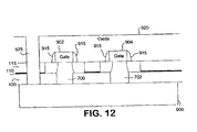
- FIG. 12 is a diagram showing formation of gate spacer and dielectric, deposition of oxide over the gate structure, and formation of a body contact in the intermediate structure of FIG. 11 , and a further intermediate structure, in an embodiment of the present invention.
- FIG. 13 is a diagram showing implantation of a contact plug in the intermediate structure of FIG. 12 , and a further intermediate structure in an embodiment of the present invention.
- FIG. 14 is a diagram showing deposition of metal in the intermediate structure of FIG. 13 to produce a back bias in an embodiment of the present invention.
- FIG. 15 shows another embodiment of the present invention.
- FIG. 16 is a diagram showing an alternative embodiment of the present invention.
- FIG. 1 shows a first step in an embodiment of a method, and an intermediate IC structure, according to the present invention.
- a first layer of oxide 100 is deposited over a Si substrate 105 .
- the thickness of oxide layer 100 is 1000 ⁇ .
- a layer of nitride (“SiN”) 110 having, in this example, but without limitation, a width of 100 ⁇ is deposited over oxide layer 100 . Acting as a stopping liner, SiN layer 110 stops the oxide etch process and prevents it from reaching material underneath SiN 110 .
- SiN 110 permits formation of a vertical T-shaped SOI structure in this embodiment.
- a second layer of oxide 115 in this embodiment having with a width of 1000 ⁇ , is deposited over the nitride layer.
- FIG. 2 shows the intermediate structure of FIG. 1 , where that intermediate structure has been etched.
- Photoresist 200 is deposited over oxide layer 115 , after which active photolithography, as known in the art, is used to etch holes in photoresist 200 .
- Photolithography as known in the art, is used to create openings in the photoresist that can eventually be used for Si epitaxial growth, for example.
- An oxide etch is then performed to etch away any oxide not underneath the photoresist. As described above, the oxide etch cannot penetrate SiN layer 110 ; thus only oxide layer 115 is etched. Oxide layer 100 , located underneath nitride layer 110 , remains unaffected.
- FIG. 3 is a diagram showing the intermediate structure of FIG. 2 following further etching.
- Photoresist layer 200 has been etched completely away, leaving behind a patterned oxide layer 115 .
- Photoresist can be removed by use of a so-called ashing process.
- FIG. 4 a layer of photoresist 400 has been deposited over the intermediate structure of FIG. 3 . Openings in photoresist 400 have been created by a photolithographic step, leaving areas of SiN layer 110 exposed.
- FIG. 5 shows the intermediate structure of FIG. 4 where that intermediate structure has been etched.
- a nitride etch is performed on the nitride 110 layer exposed by the procedure of FIG. 4 , leaving portions of oxide layer 100 exposed. Oxide etching is then performed to etch that portion of oxide layer 100 that is exposed. No other layer is affected, because photoresist 400 blocks the oxide etch from reaching materials located underneath photoresist 400 . Ashing processes are then performed on photoresist 400 to remove the remaining photoresist. Following the ashing process, a nitride etch is performed to remove any portion of nitride layer 110 exposed after photoresist 400 is removed. After the nitride etch, clean active T-shaped areas 500 and 502 , according to an aspect of the present invention, remain in the wafer.
- a thermal oxidization (not deposition) step is performed according to known methods.
- the T-shaped holes or interruptions 500 , 502 will eventually be filled with Si-epitaxy; however, for Si epitaxial growth, a clean and damage-free surface is preferred. It is possible that, while etching oxide layer 100 , the oxide etch could damage the surface at the bottom of the T-shaped interruptions 500 , 502 .
- thermal oxidation of the surface may be performed, followed by removal of the resulting thin thermal oxide 600 .
- Thin thermal oxide 600 in this example, but without limitation is about 100 ⁇ wide.
- FIG. 7 shows Si epitaxy regions grown over the T-shaped interruptions 500 , 502 in FIG. 6 to form T-shaped transistor structures 700 , 702 .
- Structures formed using Si epitaxy may grow in an uneven manner.
- CMP chemical mechanical polishing
- CMP processes ensure a smooth and even Si surface.
- a thermal oxidation step is performed over the Si epitaxy.
- the thermal oxidation forms oxide layers 800 , 802 , which, in this example, but without limitation, are about 100 ⁇ in thickness. This oxidation is used to cure Si surface damage which can occur during the CMP process.
- a well 900 is implanted into substrate 105 (not shown).
- Well 900 is used for CMOS processes, for example, to have NFET and PFET isolation.
- PFET NFET
- N well is used; whereas for an NFET, a P well is used.
- a gate is placed over the T-shaped structures. Therefore, in the illustrated embodiment, as shown in FIG. 10 , gates 902 , 904 are formed according to known methods, over the T-shaped structures 700 , 702 .
- sources and drains 910 , 912 are formed, according to known methods, e.g., by implantation on either side adjacent to gates 902 , 904 .
- T-shaped transistor structures 700 , 702 are formed according to the present invention.
- FIG. 12 shows the formation of gate spacer layers 915 and dielectric layers in the illustrated embodiment.
- Lightly doped drains (“LDD”) are used in many transistors because LDDs reduce transistors' short channel effects. Nevertheless, LDDs of separate transistors should be electrically isolated from each other.
- Gate spacers 915 electrically isolate separate LDDs from each other.
- a third layer of oxide 920 is then deposited over the transistors with gate spacer and dielectric layers.
- a back bias is created in order to remove extra holes that collect at the bottom of T-shaped structure 500 , 502 . Therefore, as shown in FIG. 12 , body contact 925 is formed, extending to Si substrate 105 (as shown in FIG. 1 ).
- a layer of photoresist is first deposited over oxide layer 920 . Photolithography, as known in the art, is then used to open a hole in the photoresist. A dry oxide etch is applied to oxide layer 920 , etching out any portion of oxide layer 920 and oxide layer 115 not underneath the photoresist. The nitride stopper layer 110 is then etched, followed by an oxide etch of oxide layer 100 , yielding body contact 925 that reaches Si substrate 105 (as shown in FIG. 1 ).
- contact plug 930 is implanted, as shown.
- Contact plug 930 is implanted with N+ dopant for an N well and P+ dopant for a P well.
- FIG. 14 shows a process for completing body contact 925 in an embodiment of the invention, in which a conductor, such as metal line 935 , is deposited to complete body contact 925 . Also, metal line 935 may be deposited over oxide layer 920 . Metal line 935 , which forms body contact 925 and contact plug 930 , in this embodiment, is inside the N+ or P+ region, leading to lower contact leakage current.
- a conductor such as metal line 935
- FIG. 15 formation of an “easy” body contact is shown in FIG. 15 .
- the contact plug 930 was deep in the body contact and, therefore, a contact plug implantation was needed.
- the embodiment shown in FIG. 15 has a contact plug that is shallow.
- a contact plug implantation is thus not necessary, since the N+ or P+ contact plug implantation is simultaneously formed during the N+ or P+ source/drain implantation. Instead, Si is grown, for example using epitaxy, in body contact 925 ′.
- an additional hole is formed, as shown in FIG. 15.
- a lower portion of body contact 925 ′ is formed with Si as shown in FIG. 15 , for example through epitaxy processes, and an upper portion of a body contact 925 ′ is also formed with a conductor, such as metal line 935 , in a process analogous to that shown in FIGS. 10 to 14 .
- the additional hole in the Si surface in FIG. 15 is implanted with N+ or P+ when the N+ or P+ source/drain implantation is formed after the gate process. This additional Si epitaxial hole process reduces the contact plug implantation step and makes an easy contact process due to the shallow contact hole.
- FIG. 16 shows another embodiment according to the present invention.
- both an easy body contact 925 ′ and a trench capacitor storage poly 940 are used.
- Storage poly 940 has a trench storage poly insulator 941 and a trench capacitor oxide 943 .
- the top of the storage poly 940 is attached to a transistor source or drain region 910 , 912 .
- the top of trench capacitor storage poly 940 has a high concentration of N-type dopant.
- This high concentration of N-type dopant degrades the cell transistor's short channel effects because of N-dopant source/drain depletion region increase by the lateral diffusion of N-dopant from the attached high N-dopant trench storage poly region 965 to channel center region 950 .
- the N-dopant diffusion is reduced since an oxide region 952 , 954 blocks N-dopant diffusion from the attached high N-dopant trench capacitor region 965 . Therefore, the short channel effects are greatly improved.
Abstract
Description
Claims (13)
Priority Applications (5)
| Application Number | Priority Date | Filing Date | Title |
|---|---|---|---|
| US10/463,023 US6930357B2 (en) | 2003-06-16 | 2003-06-16 | Active SOI structure with a body contact through an insulator |
| JP2006515959A JP2006527914A (en) | 2003-06-16 | 2004-06-16 | Silicon-on-insulator structure, method of manufacturing the same, and integrated circuit |
| CNB2004800169688A CN100373594C (en) | 2003-06-16 | 2004-06-16 | Soi shaped structure |
| EP04736907A EP1634327A1 (en) | 2003-06-16 | 2004-06-16 | Soi shaped structure |
| PCT/EP2004/006498 WO2004112127A1 (en) | 2003-06-16 | 2004-06-16 | Soi shaped structure |
Applications Claiming Priority (1)
| Application Number | Priority Date | Filing Date | Title |
|---|---|---|---|
| US10/463,023 US6930357B2 (en) | 2003-06-16 | 2003-06-16 | Active SOI structure with a body contact through an insulator |
Publications (2)
| Publication Number | Publication Date |
|---|---|
| US20040253773A1 US20040253773A1 (en) | 2004-12-16 |
| US6930357B2 true US6930357B2 (en) | 2005-08-16 |
Family
ID=33511523
Family Applications (1)
| Application Number | Title | Priority Date | Filing Date |
|---|---|---|---|
| US10/463,023 Expired - Fee Related US6930357B2 (en) | 2003-06-16 | 2003-06-16 | Active SOI structure with a body contact through an insulator |
Country Status (5)
| Country | Link |
|---|---|
| US (1) | US6930357B2 (en) |
| EP (1) | EP1634327A1 (en) |
| JP (1) | JP2006527914A (en) |
| CN (1) | CN100373594C (en) |
| WO (1) | WO2004112127A1 (en) |
Cited By (9)
| Publication number | Priority date | Publication date | Assignee | Title |
|---|---|---|---|---|
| US20050042808A1 (en) * | 2003-03-10 | 2005-02-24 | Nec Electronics Corporation | Semiconductor device and method of fabricating the same |
| US20060027877A1 (en) * | 2004-08-05 | 2006-02-09 | Kabushiki Kaisha Toshiba | Semiconductor device with triple-well region |
| US20070224789A1 (en) * | 2006-03-22 | 2007-09-27 | Samsung Electronics Co., Ltd. | Methods of fabricating silicon-on-insulator substrates having a laser-formed single crystalline film |
| US20100052053A1 (en) * | 2008-08-28 | 2010-03-04 | International Business Machines Corporation | Soi body contact using e-dram technology |
| US7985642B2 (en) | 2004-07-15 | 2011-07-26 | Infineon Technologies Ag | Formation of active area using semiconductor growth process without STI integration |
| US9203396B1 (en) | 2013-02-22 | 2015-12-01 | Triquint Semiconductor, Inc. | Radio frequency switch device with source-follower |
| US9214932B2 (en) | 2013-02-11 | 2015-12-15 | Triquint Semiconductor, Inc. | Body-biased switching device |
| US9379698B2 (en) | 2014-02-04 | 2016-06-28 | Triquint Semiconductor, Inc. | Field effect transistor switching circuit |
| US20180145088A1 (en) * | 2016-11-18 | 2018-05-24 | Globalfoundries Inc. | Field-effect transistors with a buried body contact |
Families Citing this family (4)
| Publication number | Priority date | Publication date | Assignee | Title |
|---|---|---|---|---|
| US7091071B2 (en) * | 2005-01-03 | 2006-08-15 | Freescale Semiconductor, Inc. | Semiconductor fabrication process including recessed source/drain regions in an SOI wafer |
| US7298009B2 (en) * | 2005-02-01 | 2007-11-20 | Infineon Technologies Ag | Semiconductor method and device with mixed orientation substrate |
| US8530355B2 (en) * | 2005-12-23 | 2013-09-10 | Infineon Technologies Ag | Mixed orientation semiconductor device and method |
| CN101694846B (en) * | 2009-10-14 | 2011-08-31 | 上海宏力半导体制造有限公司 | SOI-cascaded dual-tube MOS transistor structure |
Citations (14)
| Publication number | Priority date | Publication date | Assignee | Title |
|---|---|---|---|---|
| US4763183A (en) * | 1984-08-01 | 1988-08-09 | American Telephone And Telegraph Co., At&T Bell Laboratories | Semiconductor-on-insulator (SOI) devices and SOI IC fabrication method |
| US4969022A (en) * | 1987-03-20 | 1990-11-06 | Nec Corporation | Dynamic random access memory device having a plurality of improved one-transistor type memory cells |
| US5593912A (en) | 1994-10-06 | 1997-01-14 | International Business Machines Corporation | SOI trench DRAM cell for 256 MB DRAM and beyond |
| US5606188A (en) | 1995-04-26 | 1997-02-25 | International Business Machines Corporation | Fabrication process and structure for a contacted-body silicon-on-insulator dynamic random access memory |
| JPH09283766A (en) | 1996-04-18 | 1997-10-31 | Matsushita Electric Ind Co Ltd | Semiconductor device and manufacture thereof |
| US6174754B1 (en) * | 2000-03-17 | 2001-01-16 | Taiwan Semiconductor Manufacturing Company | Methods for formation of silicon-on-insulator (SOI) and source/drain-on-insulator(SDOI) transistors |
| US6245663B1 (en) * | 1998-09-30 | 2001-06-12 | Conexant Systems, Inc. | IC interconnect structures and methods for making same |
| WO2001043198A2 (en) | 1999-12-13 | 2001-06-14 | Infineon Technologies North America Corp. | Source/drain-on-insulator (s/doi) field effect transistor using silicon nitride and silicon oxide and method of fabrication |
| US6284594B1 (en) | 2000-05-30 | 2001-09-04 | Chartered Semiconductor Manufacturing Ltd. | Formation of an interpoly capacitor structure using a chemical mechanical polishing procedure |
| US6407427B1 (en) * | 1999-11-05 | 2002-06-18 | Hyundai Electronics Industries Co., Ltd. | SOI wafer device and a method of fabricating the same |
| US6429099B1 (en) | 2000-01-05 | 2002-08-06 | International Business Machines Corporation | Implementing contacts for bodies of semiconductor-on-insulator transistors |
| US20020163041A1 (en) | 2000-03-30 | 2002-11-07 | Min-Su Kim | Silicon-on-insulator (SOI) substrate, method for fabricating SOI substrate and SOI MOSFET using the SOI substrate |
| US20030134231A1 (en) * | 2002-01-15 | 2003-07-17 | Taiwan Semiconductor Manufacturing Co., Ltd. | Bi-layer photoresist dry development and reactive ion etch method |
| US6664150B2 (en) * | 2001-10-26 | 2003-12-16 | International Business Machines Corporation | Active well schemes for SOI technology |
Family Cites Families (5)
| Publication number | Priority date | Publication date | Assignee | Title |
|---|---|---|---|---|
| GB2179787B (en) * | 1985-08-26 | 1989-09-20 | Intel Corp | Buried interconnect for mos structure |
| JPS63237560A (en) * | 1987-03-26 | 1988-10-04 | Nec Corp | Insulated-gate field-effect transistor and manufacture thereof |
| JPH11307771A (en) * | 1998-04-23 | 1999-11-05 | Toshiba Corp | Semiconductor device and its manufacture |
| KR100268419B1 (en) * | 1998-08-14 | 2000-10-16 | 윤종용 | A high integrated semiconductor memory device and method fabricating the same |
| JP2002190599A (en) * | 2000-12-20 | 2002-07-05 | Toshiba Corp | Semiconductor device and method of manufacturing the same |
-
2003
- 2003-06-16 US US10/463,023 patent/US6930357B2/en not_active Expired - Fee Related
-
2004
- 2004-06-16 JP JP2006515959A patent/JP2006527914A/en active Pending
- 2004-06-16 WO PCT/EP2004/006498 patent/WO2004112127A1/en active Search and Examination
- 2004-06-16 EP EP04736907A patent/EP1634327A1/en not_active Withdrawn
- 2004-06-16 CN CNB2004800169688A patent/CN100373594C/en not_active Expired - Fee Related
Patent Citations (14)
| Publication number | Priority date | Publication date | Assignee | Title |
|---|---|---|---|---|
| US4763183A (en) * | 1984-08-01 | 1988-08-09 | American Telephone And Telegraph Co., At&T Bell Laboratories | Semiconductor-on-insulator (SOI) devices and SOI IC fabrication method |
| US4969022A (en) * | 1987-03-20 | 1990-11-06 | Nec Corporation | Dynamic random access memory device having a plurality of improved one-transistor type memory cells |
| US5593912A (en) | 1994-10-06 | 1997-01-14 | International Business Machines Corporation | SOI trench DRAM cell for 256 MB DRAM and beyond |
| US5606188A (en) | 1995-04-26 | 1997-02-25 | International Business Machines Corporation | Fabrication process and structure for a contacted-body silicon-on-insulator dynamic random access memory |
| JPH09283766A (en) | 1996-04-18 | 1997-10-31 | Matsushita Electric Ind Co Ltd | Semiconductor device and manufacture thereof |
| US6245663B1 (en) * | 1998-09-30 | 2001-06-12 | Conexant Systems, Inc. | IC interconnect structures and methods for making same |
| US6407427B1 (en) * | 1999-11-05 | 2002-06-18 | Hyundai Electronics Industries Co., Ltd. | SOI wafer device and a method of fabricating the same |
| WO2001043198A2 (en) | 1999-12-13 | 2001-06-14 | Infineon Technologies North America Corp. | Source/drain-on-insulator (s/doi) field effect transistor using silicon nitride and silicon oxide and method of fabrication |
| US6429099B1 (en) | 2000-01-05 | 2002-08-06 | International Business Machines Corporation | Implementing contacts for bodies of semiconductor-on-insulator transistors |
| US6174754B1 (en) * | 2000-03-17 | 2001-01-16 | Taiwan Semiconductor Manufacturing Company | Methods for formation of silicon-on-insulator (SOI) and source/drain-on-insulator(SDOI) transistors |
| US20020163041A1 (en) | 2000-03-30 | 2002-11-07 | Min-Su Kim | Silicon-on-insulator (SOI) substrate, method for fabricating SOI substrate and SOI MOSFET using the SOI substrate |
| US6284594B1 (en) | 2000-05-30 | 2001-09-04 | Chartered Semiconductor Manufacturing Ltd. | Formation of an interpoly capacitor structure using a chemical mechanical polishing procedure |
| US6664150B2 (en) * | 2001-10-26 | 2003-12-16 | International Business Machines Corporation | Active well schemes for SOI technology |
| US20030134231A1 (en) * | 2002-01-15 | 2003-07-17 | Taiwan Semiconductor Manufacturing Co., Ltd. | Bi-layer photoresist dry development and reactive ion etch method |
Non-Patent Citations (4)
| Title |
|---|
| Coping with the floating-body effect in SOI DRAM, Troy Robinson and Alejandro Flores; pp 1-2; http://kabuki.eecs.berkeley.edu/~troyr/class/paper/mid_proposal.html. |
| DRAM Technology for Today's Market and Future DRAM Generations; W. Neumueller, J. Alsmeier, G. Bronner, S. Ishibashi, H. Klose; www.essderc.org/papers-97/315.pdf. |
| Floating Body Effects for Design Engineers or The New Design Frontier, Ted Houston, Texas Instruments; May 25, 2000; engr.smu.edu/orgs/cas/documents/soi_ieee.ppt. |
| SOI Technology: IMB's Next Advance in Chip Design; www-3.ibm.com/chips/bluelogic/showcase/soi/soipaper.pdf. |
Cited By (18)
| Publication number | Priority date | Publication date | Assignee | Title |
|---|---|---|---|---|
| US20050042808A1 (en) * | 2003-03-10 | 2005-02-24 | Nec Electronics Corporation | Semiconductor device and method of fabricating the same |
| US7492009B2 (en) * | 2003-10-03 | 2009-02-17 | Nec Electronics Corporation | Semiconductor device having silicon on insulator structure and method of fabricating the same |
| US8173502B2 (en) | 2004-07-15 | 2012-05-08 | Infineon Technologies Ag | Formation of active area using semiconductor growth process without STI integration |
| US20110237035A1 (en) * | 2004-07-15 | 2011-09-29 | Jiang Yan | Formation of Active Area Using Semiconductor Growth Process without STI Integration |
| US7985642B2 (en) | 2004-07-15 | 2011-07-26 | Infineon Technologies Ag | Formation of active area using semiconductor growth process without STI integration |
| US7259428B2 (en) * | 2004-08-05 | 2007-08-21 | Kabushiki Kaisha Toshiba | Semiconductor device using SOI structure having a triple-well region |
| US20060027877A1 (en) * | 2004-08-05 | 2006-02-09 | Kabushiki Kaisha Toshiba | Semiconductor device with triple-well region |
| US7432173B2 (en) | 2006-03-22 | 2008-10-07 | Samsung Electronics Co., Ltd. | Methods of fabricating silicon-on-insulator substrates having a laser-formed single crystalline film |
| US20070224789A1 (en) * | 2006-03-22 | 2007-09-27 | Samsung Electronics Co., Ltd. | Methods of fabricating silicon-on-insulator substrates having a laser-formed single crystalline film |
| US20100052053A1 (en) * | 2008-08-28 | 2010-03-04 | International Business Machines Corporation | Soi body contact using e-dram technology |
| US7989893B2 (en) * | 2008-08-28 | 2011-08-02 | International Business Machines Corporation | SOI body contact using E-DRAM technology |
| US8053303B2 (en) | 2008-08-28 | 2011-11-08 | International Business Machines Corporation | SOI body contact using E-DRAM technology |
| US20110177659A1 (en) * | 2008-08-28 | 2011-07-21 | International Business Machines Corporation | Soi body contact using e-dram technology |
| US9214932B2 (en) | 2013-02-11 | 2015-12-15 | Triquint Semiconductor, Inc. | Body-biased switching device |
| US9203396B1 (en) | 2013-02-22 | 2015-12-01 | Triquint Semiconductor, Inc. | Radio frequency switch device with source-follower |
| US9379698B2 (en) | 2014-02-04 | 2016-06-28 | Triquint Semiconductor, Inc. | Field effect transistor switching circuit |
| US20180145088A1 (en) * | 2016-11-18 | 2018-05-24 | Globalfoundries Inc. | Field-effect transistors with a buried body contact |
| US10079248B2 (en) * | 2016-11-18 | 2018-09-18 | Globalfoundries Inc. | Field-effect transistors with a buried body contact |
Also Published As
| Publication number | Publication date |
|---|---|
| WO2004112127A1 (en) | 2004-12-23 |
| CN100373594C (en) | 2008-03-05 |
| US20040253773A1 (en) | 2004-12-16 |
| JP2006527914A (en) | 2006-12-07 |
| EP1634327A1 (en) | 2006-03-15 |
| CN1809920A (en) | 2006-07-26 |
Similar Documents
| Publication | Publication Date | Title |
|---|---|---|
| US6808994B1 (en) | Transistor structures and processes for forming same | |
| KR100243715B1 (en) | Cmos structure with fets having isolated wells with merged depletions and methods of making same | |
| KR100259097B1 (en) | Semiconductor device and method for fabricating the same | |
| US6518645B2 (en) | SOI-type semiconductor device and method of forming the same | |
| US6204138B1 (en) | Method for fabricating a MOSFET device structure which facilitates mitigation of junction capacitance and floating body effects | |
| US8395217B1 (en) | Isolation in CMOSFET devices utilizing buried air bags | |
| US6579750B1 (en) | Manufacturing method for fully depleted silicon on insulator semiconductor device | |
| US10211336B2 (en) | LDMOS transistor structures and integrated circuits including LDMOS transistor structures | |
| US20120267724A1 (en) | Mos semiconductor device and methods for its fabrication | |
| US6930357B2 (en) | Active SOI structure with a body contact through an insulator | |
| US20050077590A1 (en) | Guard ring structure for a Schottky diode | |
| CN112825327A (en) | Semiconductor structure and forming method thereof | |
| US6198114B1 (en) | Field effect transistor having dielectrically isolated sources and drains and method for making same | |
| US10319827B2 (en) | High voltage transistor using buried insulating layer as gate dielectric | |
| US6693018B2 (en) | Method for fabricating DRAM cell transistor having trench isolation structure | |
| US6420767B1 (en) | Capacitively coupled DTMOS on SOI | |
| KR100886708B1 (en) | Soi device and method for fabricating the same | |
| KR20120082331A (en) | Fully depleted soi device with buried doped layer | |
| US6359298B1 (en) | Capacitively coupled DTMOS on SOI for multiple devices | |
| US8530967B2 (en) | Lateral insulated-gate bipolar transistor and manufacturing method thereof | |
| JP3463593B2 (en) | Field effect transistor and method of manufacturing the same | |
| JP2891325B2 (en) | SOI semiconductor device and method of manufacturing the same | |
| KR100523053B1 (en) | Smart power device built-in SiGe HBT and fabrication method of the same | |
| KR100259593B1 (en) | A method of fabricating semiconductor device | |
| US6759308B2 (en) | Silicon on insulator field effect transistor with heterojunction gate |
Legal Events
| Date | Code | Title | Description |
|---|---|---|---|
| AS | Assignment |
Owner name: INFINEON TECHNOLOGIES NORTH AMERICA CORP., CALIFOR Free format text: ASSIGNMENT OF ASSIGNORS INTEREST;ASSIGNOR:KANG, WOO-TAG;REEL/FRAME:014395/0644 Effective date: 20030805 |
|
| AS | Assignment |
Owner name: INFINEON TECHNOLOGIES AG, GERMANY Free format text: ASSIGNMENT OF ASSIGNORS INTEREST;ASSIGNOR:INFINEON TECHNOLOGIES NORTH AMERICA CORP.;REEL/FRAME:014590/0798 Effective date: 20040430 |
|
| CC | Certificate of correction | ||
| REMI | Maintenance fee reminder mailed | ||
| FPAY | Fee payment |
Year of fee payment: 4 |
|
| SULP | Surcharge for late payment | ||
| AS | Assignment |
Owner name: QIMONDA AG, GERMANY Free format text: ASSIGNMENT OF ASSIGNORS INTEREST;ASSIGNOR:INFINEON TECHNOLOGIES AG;REEL/FRAME:023821/0535 Effective date: 20060425 Owner name: QIMONDA AG,GERMANY Free format text: ASSIGNMENT OF ASSIGNORS INTEREST;ASSIGNOR:INFINEON TECHNOLOGIES AG;REEL/FRAME:023821/0535 Effective date: 20060425 |
|
| FPAY | Fee payment |
Year of fee payment: 8 |
|
| AS | Assignment |
Owner name: INFINEON TECHNOLOGIES AG, GERMANY Free format text: ASSIGNMENT OF ASSIGNORS INTEREST;ASSIGNOR:QIMONDA AG;REEL/FRAME:035623/0001 Effective date: 20141009 |
|
| AS | Assignment |
Owner name: POLARIS INNOVATIONS LIMITED, IRELAND Free format text: ASSIGNMENT OF ASSIGNORS INTEREST;ASSIGNOR:INFINEON TECHNOLOGIES AG;REEL/FRAME:036873/0758 Effective date: 20150708 |
|
| REMI | Maintenance fee reminder mailed | ||
| LAPS | Lapse for failure to pay maintenance fees |
Free format text: PATENT EXPIRED FOR FAILURE TO PAY MAINTENANCE FEES (ORIGINAL EVENT CODE: EXP.) |
|
| STCH | Information on status: patent discontinuation |
Free format text: PATENT EXPIRED DUE TO NONPAYMENT OF MAINTENANCE FEES UNDER 37 CFR 1.362 |
|
| FP | Lapsed due to failure to pay maintenance fee |
Effective date: 20170816 |