US6946685B1 - Light emitting semiconductor method and device - Google Patents
Light emitting semiconductor method and device Download PDFInfo
- Publication number
- US6946685B1 US6946685B1 US09/652,194 US65219400A US6946685B1 US 6946685 B1 US6946685 B1 US 6946685B1 US 65219400 A US65219400 A US 65219400A US 6946685 B1 US6946685 B1 US 6946685B1
- Authority
- US
- United States
- Prior art keywords
- electrode
- migration
- semiconductor
- guard ring
- type layer
- Prior art date
- Legal status (The legal status is an assumption and is not a legal conclusion. Google has not performed a legal analysis and makes no representation as to the accuracy of the status listed.)
- Expired - Lifetime, expires
Links
Images


Classifications
-
- H—ELECTRICITY
- H01—ELECTRIC ELEMENTS
- H01L—SEMICONDUCTOR DEVICES NOT COVERED BY CLASS H10
- H01L33/00—Semiconductor devices with at least one potential-jump barrier or surface barrier specially adapted for light emission; Processes or apparatus specially adapted for the manufacture or treatment thereof or of parts thereof; Details thereof
- H01L33/36—Semiconductor devices with at least one potential-jump barrier or surface barrier specially adapted for light emission; Processes or apparatus specially adapted for the manufacture or treatment thereof or of parts thereof; Details thereof characterised by the electrodes
- H01L33/40—Materials therefor
- H01L33/405—Reflective materials
-
- H—ELECTRICITY
- H01—ELECTRIC ELEMENTS
- H01L—SEMICONDUCTOR DEVICES NOT COVERED BY CLASS H10
- H01L2224/00—Indexing scheme for arrangements for connecting or disconnecting semiconductor or solid-state bodies and methods related thereto as covered by H01L24/00
- H01L2224/01—Means for bonding being attached to, or being formed on, the surface to be connected, e.g. chip-to-package, die-attach, "first-level" interconnects; Manufacturing methods related thereto
- H01L2224/42—Wire connectors; Manufacturing methods related thereto
- H01L2224/47—Structure, shape, material or disposition of the wire connectors after the connecting process
- H01L2224/49—Structure, shape, material or disposition of the wire connectors after the connecting process of a plurality of wire connectors
- H01L2224/491—Disposition
- H01L2224/49105—Connecting at different heights
- H01L2224/49107—Connecting at different heights on the semiconductor or solid-state body
-
- H—ELECTRICITY
- H01—ELECTRIC ELEMENTS
- H01L—SEMICONDUCTOR DEVICES NOT COVERED BY CLASS H10
- H01L33/00—Semiconductor devices with at least one potential-jump barrier or surface barrier specially adapted for light emission; Processes or apparatus specially adapted for the manufacture or treatment thereof or of parts thereof; Details thereof
- H01L33/02—Semiconductor devices with at least one potential-jump barrier or surface barrier specially adapted for light emission; Processes or apparatus specially adapted for the manufacture or treatment thereof or of parts thereof; Details thereof characterised by the semiconductor bodies
- H01L33/26—Materials of the light emitting region
- H01L33/30—Materials of the light emitting region containing only elements of group III and group V of the periodic system
- H01L33/32—Materials of the light emitting region containing only elements of group III and group V of the periodic system containing nitrogen
Definitions
- This invention relates to light emitting semiconductor structures and methods of making same and, more particularly, to devices and methods employing III-V nitride semiconductors and to improving the operation thereof.
- Light emitting semiconductors which emit in several regions of the visible spectrum, for example group III-V semiconductors such as aluminum gallium arsenide and gallium phosphide, have achieved commercial acceptance for various applications.
- group III-V semiconductors such as aluminum gallium arsenide and gallium phosphide
- efficient semiconductor light emitters have been sought for shorter visible wavelengths. If such solid state light emitting sources were available at reasonable cost, many lighting applications could benefit from the reliability and low energy consumption that characterize semiconductor operation.
- Short wavelength devices also hold promise of providing increased storage capacity on storage media, due to the ability to obtain smaller spot sizes for writing and reading on the media.
- Blue light-emitting diodes utilizing silicon carbide were developed during the early 1990's, but exhibited indirect bandgap luminance which limited the practicality of the devices.
- Zinc selenide, a group II-VI material also produces blue light emission.
- silicon carbide devices, as well as zinc selenide blue light emitting diodes have been found to exhibit relatively short lifetimes that limit their usefulness.
- a type of short wavelength light emitting devices that has direct energy bandgap, and has shown excellent promise, is based on group III-V nitride semiconductors, which include substances such as GaN, AlN, InN, AlInN, GaInN, AlGaN, AlInGaN, BAlN, BInN, BGaN, and BAlGaInN, among others.
- group III-V nitride semiconductors which include substances such as GaN, AlN, InN, AlInN, GaInN, AlGaN, AlInGaN, BAlN, BInN, BGaN, and BAlGaInN, among others.
- An example of a light emitting device of this type is set forth in European Patent Publication EP 0926744, which discloses a light emitting device that has an active region between an n-type layer of III-V nitride semiconductor and a p-type layer of III-V nitride semiconductor.
- the wallplug efficiency of the light emitting diode (LED) structure is defined by the optical power emitted by the device per unit of electric power. To maximize efficiency, both the light generated per watt of drive power and the amount of light exiting from the LED in a useful direction are considered.
- the resistance of the p-type III-V nitride semiconductor layer is much higher than the resistance of the n-type III-V nitride semiconductor layer.
- the p-electrode junction with the p-type layer is inherently more resistive than the n-electrode junction with the n-type layer.
- the p-electrode is generally made much larger than the n-electrode.
- the p-layer can be a layer of silver that is sufficiently thin to be transparent. It is noted that silver advantageously forms an ohmic contact at the p-type III-V nitride semiconductor layers.
- a metal bonding pad is deposited on the silver electrode.
- the silver layer is thick enough to reflect most of the light incident thereon, and light exits via the substrate.
- a fixation layer such as another metal layer, which can be nickel, can be applied over and on the sides, of the silver layer, and prevents the diffusion of the metal (e.g. gold) of the contact bonding pad into the silver layer.
- the diffusion barrier layer is also stated to improve the stability underlying silver layer and improve the mechanical and electrical characteristics of the silver layer. As a result, it is stated that the substrate temperature during the vapor deposition step in which the silver layer is formed can be lowered and the vapor deposition speed increased.
- the p-contact (that is, the electrode coupled to the p-type layer of III-V nitride semiconductor) comprises a metal layer, or multiple metal layers, having a pattern of small openings.
- the metal or metals used are preferably selected from the group consisting of silver, aluminum, and rhodium, and alloys thereof.
- An illustrated electrode or contact is a perforated silver mesh obtained by etching a pattern of holes in a silver layer.
- An optional dielectric encapsulant preferably having an index of refraction greater than 1.5, such as silicon dioxide, silicon nitride, aluminum nitride, aluminum oxide, hafnium oxide, or titanium oxide, may be deposited over the p-contact.
- the encapsulant allows light to be reflected internally above rather than below the silver mirror, which increases its chance for escape without attenuation.
- the encapsulant improves the adhesion of the silver film to the LED surface by tacking down the metal at the open spaces across the surface.
- the dielectric also protects the metal layer from scratches that may occur during fabrication, and protects it from environmental degradation such as oxidation or tarnishing.
- LED's were designed, when using opaque contacts (or contact pads), to have the contacts be as small as possible to minimize obscuration of the surface of the LED.
- the finely patterned electrode can cover the entire surface, or as much thereof as desired, and also can be made as thick as necessary, both of these characteristics serving to minimize contact resistance.
- light can escape through the small openings in the silver electrode, either directly or after one or more reflections. Use of the small openings is not necessarily preferred at present.
- the silver electrode metallization is subject to electrochemical migration in the presence of moisture and an electric field, such as, for example, the field developed as a result of applying an operating voltage at the contacts of the device. Electrochemical migration of the silver metallization to the pn junction of the device results in an alternate shunt path across the junction, which degrades efficiency of the device.
- a light-emitting device which comprises a semiconductor structure having a plurality of semiconductor layers and including an active region within the layers.
- First and second conductive metal electrodes contact respectively different semiconductor layers of the structure.
- a migration barrier is provided for preventing migration of metal from at least one of said electrodes onto the surface of the semiconductor layer with which said at least one electrode is in contact.
- a light emitting device which comprises a semiconductor structure that includes a light-emitting active region between an n-type layer of III-V nitride semiconductor and a p-type layer of III-V nitride semiconductor.
- a p-electrode comprising silver metal is deposited on the p-type layer, and an n-electrode is coupled with the n-type layer.
- Means are provided by which electrical signals can be applied across said electrodes to cause light emission from the active region, and a migration barrier is provided for preventing electrochemical migration of silver metal from the p-electrode toward the active region.
- the migration barrier comprises a guard ring the periphery of the p-electrode or a guard sheet covering the p-electrode.
- the guard ring or guard sheet preferably comprises a conductive material such as a conductive metal or semiconductor that is not susceptible to electrochemical migration under pertinent conditions.
- FIG. 1 is a cross-sectional view of a device of the type set forth in the copending U.S. patent application Ser. No. 09/151,554, and in which improvements in accordance with embodiments of the invention can be implemented.
- FIG. 2 is a top view, partially in plan form, of the FIG. 1 device.
- FIG. 3 is a simplified cross-section of the device of FIGS. 1 and 2 .
- FIG. 4 is another simplified cross-sectional view that is useful in understanding a problem of electrochemical migration that is reduced or eliminated by the invention.
- FIGS. 5 and 6 are scanning electron microscope (SEM) photographs of an edge of the device of FIGS. 1 and 2 , before stress testing, showing the mesh metallization and the junction, and wherein it can be seen that silver metal has not migrated toward the pn junction.
- FIGS. 7 and 8 are SEM photographs of a corner of the device of FIGS. 1 and 2 after the stress of accelerated reliability testing, which show the migration of silver to the pn junction.
- FIG. 9 is a graph of light output versus forward current for a device before and after stressing, illustrating the deterioration of light output for the device which suffered the electrochemical migration of silver to the pn junction due to the stress of the accelerated reliability testing.
- FIG. 10 is a graph of current versus voltage for a device before and after stressing, illustrating the collapse of the I-V curve for the device after the stress of testing.
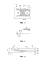
- FIG. 11 is a top view, partially in plan form, of a device including the improvement of an embodiment of the invention.
- FIG. 12 shows a simplified cross-sectional view of the FIG. 11 device.
- FIG. 13 is a simplified cross-section of the device of FIG. 11 or FIG. 12 , useful in understanding how the improvement of the invention operates to reduce or eliminate electrochemical migration of silver metal.
- FIG. 14 is another simplified cross sectional view of a device with a mesh electrode, showing how a guard ring in accordance with an embodiment of the invention can be employed.
- FIG. 15 illustrate another embodiment of the invention, employing a guard sheet.
- FIG. 16 shows a simplified cross sectional view of a device in accordance with a further embodiment of the invention.
- FIG. 17 shows a simplified cross-sectional view of a portion of a device in accordance with a still further embodiment of the invention.
- FIG. 1 illustrates a III-V nitride light emitting diode (LED) 110 that includes a bottom reflective layer 112 , a substrate 115 , which may be for example a sapphire, SiC, or GaN substrate, an n-type layer 120 of a III-V nitride semiconductor for example n-type GaN, and a p-type layer 140 of a III-V nitride semiconductor for example p-type GaN.
- the active region 130 can be the p-n junction itself or, more typically, a single quantum well or multiple quantum wells of III-V nitride between barrier layers of another III-V nitride, for example using InGaN and AlGaN.
- any suitable III-V nitride semiconductors can be used for any of the semiconductor layers of the device, and that suitable additional semiconductor layers can be employed in the device.
- a conductive metal electrode 150 (the n-electrode) is deposited on the n-type layer 120 and a conductive metal electrode 160 (the p-electrode) is deposited on the p-type layer 140 .
- the p-electrode conventionally is of much larger area than the n-electrode.
- the p-electrode 160 and the reflector 112 can comprise silver metal, which has advantageous electrically conductive and light reflective properties, and can form an ohmic contact with the p-type layer 140 .
- the silver electrode 160 can comprise a silver mesh with a pattern of openings, as described in the above-referenced copending Application.
- the finely patterned electrode can cover the entire surface of the p-layer, or as much thereof as desired, and can be made as thick as necessary (both of these characteristics serving to minimize contact resistance), and light can escape through the openings in the p-electrode, either directly or after one or more reflections.
- a contact pad 161 is deposited on the p-electrode to 160 .
- Leads 116 and 117 are respectively attached to the electrode (or contact) 150 and the contact pad 116 , and suitable electrical potentials can be applied across the leads.
- FIG. 2 shows a top view of a device of the general type shown in FIG. 1
- FIG. 3 is a simplified cross-sectional view of part of the FIG. 2 device.
- the silver mesh p-electrode is labeled 160
- the p-contact pad is labeled 161 ( FIG. 2 )
- the n-electrode is labeled 150 .
- the p-type layer is again represented at 140
- the n-type layer is again represented at 120
- the pn junction (where active region layers, not shown in this simplified diagram, can be located) is represented at 130 A.
- the silver electrode metallization is subject to electrochemical migration in the presence of moisture and an electric field, such as the field developed as a result of applying an operating voltage at the contacts of the device. Electrochemical migration of the silver metallization to the pn junction of the device results in an alternate shunt path across the junction, which degrades efficiency of the device.
- FIG. 4 illustrates the type of potential gradient that occurs adjacent an exemplary silver electrode 160 and causes migration of silver toward the pn junction.
- the n-contact 150 to an exemplary n-type layer 120 is at ground potential and that an exemplary p-electrode layer 160 (silver, in this case) is at a potential +V.
- the equipotential surfaces (seen as lines in the cross-section of FIG. 4 ) in the exemplary p-type layer 140 (p-type GaN, in this example, which generally has much higher resistivity than n-type GaN), are shown in the Figure as being at potentials V 1 , V 2 , V 3 , . . .
- the dissolved silver cations migrate along the surface of the layer 140 and toward the pn junction (at which exemplary active region 130 is located in this example), where it can provide a shunt path that deteriorates device operation.
- FIGS. 5 through 10 are SEM photographs of a device of the type diagramed in FIG. 2 , prior to accelerated reliability testing.
- FIG. 5 shows at, ⁇ 500 magnification, from top to bottom, the silver mesh electrode, the p-type layer, the pn junction (curved heavy white line), and the n-type layer.
- FIG. 6 is a similar SEM photograph at higher magnification ( ⁇ 2000). In these photographs, no migration of silver to the pn junction is evident.
- FIGS. 5 and 6 are SEM photographs of a device of the type diagramed in FIG. 2 , prior to accelerated reliability testing.
- FIG. 5 shows at, ⁇ 500 magnification, from top to bottom, the silver mesh electrode, the p-type layer, the pn junction (curved heavy white line), and the n-type layer.
- FIG. 6 is a similar SEM photograph at higher magnification ( ⁇ 2000). In these photographs, no migration of silver to the pn junction is evident.
- FIG. 7 and 8 are SEM photographs (at ⁇ 2,500 and ⁇ 16,000 magnifications, respectively) of a similar light emitting diode device after accelerated reliability testing under conditions of 85 degrees C., 85% RH, at 20 mA DC. Silver migration was confirmed by EDX, showing silver droplets (bright spots) forming at the pn junction.
- FIG. 9 is a graph of light output (L) as a function of forward current (I) for the devices of FIGS. 5 , 6 (before accelerated reliability testing—square shaped points in the FIG. 9 graph) and FIGS. 7 , 8 (after accelerated reliability testing—circular shaped points in the FIG. 9 graph).
- FIG. 10 shows forward bias IV curves (using the same graph point symbols for the respective device states; that is, square shaped points for before the stress of reliability testing, and circular shaped points for after the stress of the testing) which demonstrate collapse of the I-V curve for the stressed device, indicative of an alternate conduction path shunting the pn junction.
- FIGS. 11 and 12 illustrate an embodiment of the invention that employs a migration barrier to prevent migration of the electrode metal, (silver, in this embodiment) toward the pn junction.
- the migration barrier is a guard ring 170 formed around the periphery of the p-electrode 160 .
- the guard ring is preferably a material of high electrical conductivity, such as a conductive metal.
- the guard ring 170 preferably surrounds the entire periphery of the electrode.
- FIG. 13 illustrates how the migration barrier of embodiments hereof, in the form of a conductive guard ring and/or guard sheet, operates to prevent the deleterious migration of metal along the surface of the p-type layer 140 and toward the active region at the pn junction.
- the edge of the silver p-electrode 160 along the line where its periphery contacts the p-layer 140 , is surrounded by the guard ring 170 .
- the p-electrode is again at a potential +V, so the conductive metal guard ring will also be at the potential +V.
- the equipotential surfaces are shown as being at potentials V 1 , V 2 , V 3 . . . where V>V 1 >V 2 >V 3 . . .
- the surface of p-type layer 160 around the periphery of silver electrode 160 (and under the guard ring 170 ) will be at substantially the potential +V, and there will be little, if any, potential gradient at the edge of the silver electrode 160 that could cause silver to migrate along the surface of the p-layer and toward the pn junction of the device.
- any highly conductive material may be used as a guard ring or as a guard sheet (to be described).
- the metals Ni, Ti, W, Al Cr, Cu, Au, S, Rh, Re, Ru, or combinations or alloys thereof, may be used.
- certain stable conducting and semiconducting compounds may be used, for example the metal suicides, metal nitrides, or highly doped semiconductors.
- the properties needed are (1) adherence to the silver and the p-type III-V nitride semiconductor; (2) sufficient conductivity to nullify the electrical field at the silver boundary; (3) a compatible method of deposition; (4) a compatible method of patterning the material; (5) absence of electrochemical migration for the selected material in the presence of an electrical field in a moist environment; and (6) controlled mutual solubility and reactivity with respect to the silver.
- the listed materials are exemplary, and that other suitable materials can be used.
- FIG. 14 shows a simplified cross-sectional view taken through a section defined by arrows 14 — 14 of FIG. 11 , and including illustration of a pattern of openings 167 in the p-electrode, as described in the above-referenced copending U.S. patent application Ser. No. 09/151,554.
- the metal guard ring 170 is seen to be configured such that the transmissivity through the openings of the electrode is unaffected.
- FIG. 15 shows a further embodiment wherein the migration barrier is a conducting guard sheet 175 .
- the guard sheet could also be employed in conjunction with a transparent, or partially transmissive p-electrode by providing an optically transmissive conductive guard sheet using, for example, indium tin oxide.
- the guard ring or guard sheet conductor should encompass the silver thoroughly such that there is no surface electrical pathway from the pn junction to the silver that is not intercepted by the guard conductor. In other words, all the edges of the silver should preferably be covered by the guard conductor.
- a guard sheet should preferably cover the entirety of the underlying silver so as to provide a physical barrier to etchants and other substances from penetrating to and subsequently reacting with said silver layer during the operational life of the structure. In the case where the p-metal is intended to be opaque, then complete encapsulation of the silver by the guard conductor is the simplest and most effective (e.g. FIG.
- guard ring geometry can also perform adequately.
- the guard ring geometry is preferred unless the guard conductor is optically transparent at the wavelengths of interest.
- a transparent guard sheet indium tin oxide, for example may be used.
- the guard sheet may contain additional layers or materials which enhance electrical connections or device fabrication in other ways.
- additional layers or materials which enhance electrical connections or device fabrication in other ways.
- a layer of material that is chemically reactive with ionic silver species may be included. This reaction would form an insoluble immobile silver species from the ionic species.
- Other purposes for including additional layers may be to enhance connection to conductors, soldering to other substrates or chip mounting schemes, or interconnection of adjacent devices.
- FIG. 16 shows a further embodiment of the invention in which the migration barrier is held at a potential that tends to repulse ions back toward the p-electrode from which they would otherwise tend to migrate.
- the illustrated embodiment shows n-type layer 120 (n-type GaN, for example), p-type layer 140 (p-type GaN, for example), and active region 130 therebetween.
- the silver p-electrode is represented at 160 and the n-electrode is represented at 155 .
- the migration barrier in this embodiment is a guard ring 190 , spaced from the p-electrode, on the p-type layer 140 .
- the p-electrode is at a voltage V 3
- the n-electrode is at a voltage V 1
- the guard ring is at a voltage V 2 , where V 2 >V 3 >V 1 .
- the guard ring or guard sheet can also comprise a structure of multiple layers of conducting metals and semiconductors in combination with each other and in possible combination with dielectric interspersing layers which may incorporate vias through which electrical connection between conducting layers can be achieved.
- the guard sheet hereof can also serve the purpose of encapsulating and protecting the silver.
- the following further materials are noted: titanium nitride, tungsten nitride, and nitrogenated titanium-tungsten alloy. These and other suitable materials can be deposited by techniques such as sputtering, evaporation, or chemical vapor deposition. Applicant has noted that coverage of the silver electrode “step” can become compromised by cracking, accentuated grain boundaries, or other material defects, especially adjacent the top edge of the silver electrode. This crack or other defect can provide a path through contaminants, and moisture can penetrate to the silver layer and react with it.
- FIG. 17 addresses and solves this problem.
- the Figure shows p-type layer 140 (p-type GaN, for example) with a silver p-electrode 160 thereon.
- An edge protector 1791 is deposited over the edge of the electrode, and the guard sheet (or ring) 1792 covers the edge protector and at least part of the electrode.
- the edge protector does not have to be conducting so long as electrical connection can be made to the final deposited, conducting guard sheet.
- a material which deposits over the defined silver such that it covers the edge of the silver without cracking would preferentially be chosen.
- This edge protector is also preferably a material over which the final guard sheet can be deposited such that good step coverage of the guard sheet over the edges of the edge protector can be achieved.
- a suitable dielectric such as Al 2 O 3 can be utilized for the edge protector.
Abstract
Description
V>V 1 >V 2 >V 3 . . .
Accordingly, the dissolved silver cations, under the influence of this potential gradient, migrate along the surface of the
V>V 1 >V 2 >V 3 . . .
In this case, the surface of p-
Claims (35)
Priority Applications (1)
| Application Number | Priority Date | Filing Date | Title |
|---|---|---|---|
| US09/652,194 US6946685B1 (en) | 2000-08-31 | 2000-08-31 | Light emitting semiconductor method and device |
Applications Claiming Priority (1)
| Application Number | Priority Date | Filing Date | Title |
|---|---|---|---|
| US09/652,194 US6946685B1 (en) | 2000-08-31 | 2000-08-31 | Light emitting semiconductor method and device |
Publications (1)
| Publication Number | Publication Date |
|---|---|
| US6946685B1 true US6946685B1 (en) | 2005-09-20 |
Family
ID=34991951
Family Applications (1)
| Application Number | Title | Priority Date | Filing Date |
|---|---|---|---|
| US09/652,194 Expired - Lifetime US6946685B1 (en) | 2000-08-31 | 2000-08-31 | Light emitting semiconductor method and device |
Country Status (1)
| Country | Link |
|---|---|
| US (1) | US6946685B1 (en) |
Cited By (19)
| Publication number | Priority date | Publication date | Assignee | Title |
|---|---|---|---|---|
| US20050194603A1 (en) * | 2001-07-23 | 2005-09-08 | Slater David B.Jr. | Light emitting diodes including barrier layers/sublayers and manufacturing methods therefor |
| US20080252212A1 (en) * | 2004-09-09 | 2008-10-16 | Toyoda Gosei Co., Ltd. | Solid state device and light-emitting element |
| US20100164103A1 (en) * | 2008-12-26 | 2010-07-01 | Sumitomo Electric Device Innovations, Inc. | Semiconductor device |
| US7772604B2 (en) | 2006-01-05 | 2010-08-10 | Illumitex | Separate optical device for directing light from an LED |
| US7789531B2 (en) | 2006-10-02 | 2010-09-07 | Illumitex, Inc. | LED system and method |
| US7829358B2 (en) | 2008-02-08 | 2010-11-09 | Illumitex, Inc. | System and method for emitter layer shaping |
| US20110018015A1 (en) * | 2009-07-21 | 2011-01-27 | Koninklijke Philips Electronics N.V. | Contact for a semiconductor light emitting device |
| US8115217B2 (en) | 2008-12-11 | 2012-02-14 | Illumitex, Inc. | Systems and methods for packaging light-emitting diode devices |
| WO2012028511A1 (en) * | 2010-08-31 | 2012-03-08 | Osram Opto Semiconductors Gmbh | Optoelectronic semiconductor chip and method for producing an optoelectronic semiconductor chip |
| CN102569122A (en) * | 2012-03-05 | 2012-07-11 | 复旦大学 | Structure and method for testing quality of LED (Light Emitting Diode) side passivation layer |
| US20120199863A1 (en) * | 2009-06-25 | 2012-08-09 | Koninklijke Philips Electronics N.V. | Contact for a semiconductor light emitting device |
| US8449128B2 (en) | 2009-08-20 | 2013-05-28 | Illumitex, Inc. | System and method for a lens and phosphor layer |
| US8585253B2 (en) | 2009-08-20 | 2013-11-19 | Illumitex, Inc. | System and method for color mixing lens array |
| EP2797127A3 (en) * | 2013-04-25 | 2015-11-04 | Stanley Electric Co., Ltd. | Semiconductor light emitting element |
| US9306124B2 (en) | 2012-05-17 | 2016-04-05 | Epistar Corporation | Light emitting device with reflective electrode |
| US9312449B2 (en) | 2012-10-31 | 2016-04-12 | Xiamen Sanan Optoelectronics Technology Co., Ltd. | Light-emitting device with reflecting electrode |
| CN105489721A (en) * | 2015-09-21 | 2016-04-13 | 大连德豪光电科技有限公司 | LED flip chip comprising reflecting layer and preparation method of LED flip chip |
| CN105489742A (en) * | 2015-09-21 | 2016-04-13 | 大连德豪光电科技有限公司 | LED flip chip and preparation method thereof |
| CN106025033A (en) * | 2016-06-30 | 2016-10-12 | 大连德豪光电科技有限公司 | LED flip chip and preparation method thereof |
Citations (23)
| Publication number | Priority date | Publication date | Assignee | Title |
|---|---|---|---|---|
| US4153905A (en) | 1977-04-01 | 1979-05-08 | Charmakadze Revaz A | Semiconductor light-emitting device |
| US4210389A (en) | 1978-11-14 | 1980-07-01 | Mcdonnell Douglas Corporation | Bond and method of making the same |
| US4347655A (en) | 1978-09-28 | 1982-09-07 | Optical Information Systems, Inc. | Mounting arrangement for semiconductor optoelectronic devices |
| DE3725454A1 (en) | 1987-07-31 | 1989-02-09 | Siemens Ag | ELECTRICAL MULTI-LAYER COMPONENT WITH A SINTERED, MONOLITHIC CERAMIC BODY AND METHOD FOR PRODUCING THE ELECTRICAL MULTI-LAYER COMPONENT |
| US4817854A (en) | 1985-03-11 | 1989-04-04 | The United States Of America As Represented By The Secretary Of The Air Force | LED soldering method utilizing a PT migration barrier |
| US4990970A (en) | 1990-01-16 | 1991-02-05 | General Motors Corporation | Light emitting semiconductor having a rear reflecting surface |
| US5055893A (en) | 1990-04-23 | 1991-10-08 | Eastman Kodak Company | Light-emitting diode array with reflective layer |
| US5132750A (en) | 1989-11-22 | 1992-07-21 | Daido Tokushuko Kabushiki Kaisha | Light-emitting diode having light reflecting layer |
| US5237581A (en) | 1990-11-14 | 1993-08-17 | Nec Corporation | Semiconductor multilayer reflector and light emitting device with the same |
| US5414281A (en) | 1992-08-25 | 1995-05-09 | Mitsubishi Cable Industries, Ltd. | Semiconductor light emitting element with reflecting layers |
| US5460911A (en) | 1994-03-14 | 1995-10-24 | Xerox Corporation | Electrophotographic imaging member free of reflection interference |
| WO1996009653A1 (en) | 1994-09-20 | 1996-03-28 | Cree Research Inc. | Vertical geometry light emitting diode with group iii nitride active layer and extended lifetime |
| US5537433A (en) | 1993-07-22 | 1996-07-16 | Sharp Kabushiki Kaisha | Semiconductor light emitter |
| US5563422A (en) | 1993-04-28 | 1996-10-08 | Nichia Chemical Industries, Ltd. | Gallium nitride-based III-V group compound semiconductor device and method of producing the same |
| DE19537545A1 (en) | 1995-10-09 | 1997-04-10 | Telefunken Microelectron | Luminescence diode manufacturing method with layer group contg. pre-junction |
| DE19648309A1 (en) | 1995-12-21 | 1997-07-03 | Hewlett Packard Co | Reflecting contact device for semiconductor light emitting diode |
| US5760479A (en) | 1996-02-29 | 1998-06-02 | Texas Instruments Incorporated | Flip-chip die attachment for a high temperature die to substrate bond |
| US5854087A (en) | 1993-04-27 | 1998-12-29 | Nec Corporation | Method of manufacturing an optical semiconductor device |
| EP0905797A2 (en) | 1997-09-29 | 1999-03-31 | Siemens Aktiengesellschaft | Semiconductor light source and method of fabrication |
| EP0926744A2 (en) | 1997-12-15 | 1999-06-30 | Hewlett-Packard Company | Light emitting device |
| DE19921987A1 (en) | 1998-05-13 | 1999-11-18 | Toyoda Gosei Kk | Light-radiating flip chip semiconductor device |
| US6091085A (en) | 1998-02-19 | 2000-07-18 | Agilent Technologies, Inc. | GaN LEDs with improved output coupling efficiency |
| US6222207B1 (en) * | 1999-05-24 | 2001-04-24 | Lumileds Lighting, U.S. Llc | Diffusion barrier for increased mirror reflectivity in reflective solderable contacts on high power LED chip |
-
2000
- 2000-08-31 US US09/652,194 patent/US6946685B1/en not_active Expired - Lifetime
Patent Citations (26)
| Publication number | Priority date | Publication date | Assignee | Title |
|---|---|---|---|---|
| US4153905A (en) | 1977-04-01 | 1979-05-08 | Charmakadze Revaz A | Semiconductor light-emitting device |
| US4347655A (en) | 1978-09-28 | 1982-09-07 | Optical Information Systems, Inc. | Mounting arrangement for semiconductor optoelectronic devices |
| US4210389A (en) | 1978-11-14 | 1980-07-01 | Mcdonnell Douglas Corporation | Bond and method of making the same |
| US4817854A (en) | 1985-03-11 | 1989-04-04 | The United States Of America As Represented By The Secretary Of The Air Force | LED soldering method utilizing a PT migration barrier |
| DE3725454A1 (en) | 1987-07-31 | 1989-02-09 | Siemens Ag | ELECTRICAL MULTI-LAYER COMPONENT WITH A SINTERED, MONOLITHIC CERAMIC BODY AND METHOD FOR PRODUCING THE ELECTRICAL MULTI-LAYER COMPONENT |
| US5132750A (en) | 1989-11-22 | 1992-07-21 | Daido Tokushuko Kabushiki Kaisha | Light-emitting diode having light reflecting layer |
| US4990970A (en) | 1990-01-16 | 1991-02-05 | General Motors Corporation | Light emitting semiconductor having a rear reflecting surface |
| US5055893A (en) | 1990-04-23 | 1991-10-08 | Eastman Kodak Company | Light-emitting diode array with reflective layer |
| US5237581A (en) | 1990-11-14 | 1993-08-17 | Nec Corporation | Semiconductor multilayer reflector and light emitting device with the same |
| US5414281A (en) | 1992-08-25 | 1995-05-09 | Mitsubishi Cable Industries, Ltd. | Semiconductor light emitting element with reflecting layers |
| US5854087A (en) | 1993-04-27 | 1998-12-29 | Nec Corporation | Method of manufacturing an optical semiconductor device |
| US5563422A (en) | 1993-04-28 | 1996-10-08 | Nichia Chemical Industries, Ltd. | Gallium nitride-based III-V group compound semiconductor device and method of producing the same |
| US5537433A (en) | 1993-07-22 | 1996-07-16 | Sharp Kabushiki Kaisha | Semiconductor light emitter |
| US5460911A (en) | 1994-03-14 | 1995-10-24 | Xerox Corporation | Electrophotographic imaging member free of reflection interference |
| WO1996009653A1 (en) | 1994-09-20 | 1996-03-28 | Cree Research Inc. | Vertical geometry light emitting diode with group iii nitride active layer and extended lifetime |
| DE19537545A1 (en) | 1995-10-09 | 1997-04-10 | Telefunken Microelectron | Luminescence diode manufacturing method with layer group contg. pre-junction |
| US5917202A (en) | 1995-12-21 | 1999-06-29 | Hewlett-Packard Company | Highly reflective contacts for light emitting semiconductor devices |
| DE19648309A1 (en) | 1995-12-21 | 1997-07-03 | Hewlett Packard Co | Reflecting contact device for semiconductor light emitting diode |
| US5760479A (en) | 1996-02-29 | 1998-06-02 | Texas Instruments Incorporated | Flip-chip die attachment for a high temperature die to substrate bond |
| EP0905797A2 (en) | 1997-09-29 | 1999-03-31 | Siemens Aktiengesellschaft | Semiconductor light source and method of fabrication |
| US6111272A (en) | 1997-09-29 | 2000-08-29 | Siemens Aktiengesellschaft | Semiconductor light source formed of layer stack with total thickness of 50 microns |
| EP0926744A2 (en) | 1997-12-15 | 1999-06-30 | Hewlett-Packard Company | Light emitting device |
| US6194743B1 (en) * | 1997-12-15 | 2001-02-27 | Agilent Technologies, Inc. | Nitride semiconductor light emitting device having a silver p-contact |
| US6091085A (en) | 1998-02-19 | 2000-07-18 | Agilent Technologies, Inc. | GaN LEDs with improved output coupling efficiency |
| DE19921987A1 (en) | 1998-05-13 | 1999-11-18 | Toyoda Gosei Kk | Light-radiating flip chip semiconductor device |
| US6222207B1 (en) * | 1999-05-24 | 2001-04-24 | Lumileds Lighting, U.S. Llc | Diffusion barrier for increased mirror reflectivity in reflective solderable contacts on high power LED chip |
Non-Patent Citations (4)
| Title |
|---|
| G.E. Höfler et al., "High-flux high-efficency transparent-substrate AlGalnP/GaP light-emitting diodes", Electronics Letters, 3<SUP>rd </SUP>Sep. 1998, vol. 34, No. 18, pp. 1-2. |
| J.J. Steppan et al., "A Review Of Corrosion Failure Mechanisms During Accelerated Tests", vol. 134, No. 1, Jan. 1987. |
| K.D. Hobart et al., J. Electrochem. Soc. 146, 3833-3836, 1999. |
| Mensz et al., Electronic Letters 33 (24) pp. 2066-2068, 1997. |
Cited By (42)
| Publication number | Priority date | Publication date | Assignee | Title |
|---|---|---|---|---|
| US20050194603A1 (en) * | 2001-07-23 | 2005-09-08 | Slater David B.Jr. | Light emitting diodes including barrier layers/sublayers and manufacturing methods therefor |
| US20070161137A1 (en) * | 2001-07-23 | 2007-07-12 | Cree, Inc. | Methods of manufacturing light emitting diodes including barrier layers/sublayers |
| US8269241B2 (en) * | 2001-07-23 | 2012-09-18 | Cree, Inc. | Light emitting diodes including barrier layers/sublayers and manufacturing methods therefor |
| US8907366B2 (en) | 2001-07-23 | 2014-12-09 | Cree, Inc. | Light emitting diodes including current spreading layer and barrier sublayers |
| US7611915B2 (en) | 2001-07-23 | 2009-11-03 | Cree, Inc. | Methods of manufacturing light emitting diodes including barrier layers/sublayers |
| US20100006883A1 (en) * | 2001-07-23 | 2010-01-14 | Cree,Inc. | Light emitting diodes including barrier layers/sublayers and manufacturing methods therefor |
| US8604502B2 (en) | 2001-07-23 | 2013-12-10 | Cree, Inc. | Light emitting diodes including barrier sublayers |
| US7211833B2 (en) * | 2001-07-23 | 2007-05-01 | Cree, Inc. | Light emitting diodes including barrier layers/sublayers |
| US8017967B2 (en) * | 2004-09-09 | 2011-09-13 | Toyoda Gosei Co., Ltd. | Light-emitting element including a fusion-bonding portion on contact electrodes |
| US20080252212A1 (en) * | 2004-09-09 | 2008-10-16 | Toyoda Gosei Co., Ltd. | Solid state device and light-emitting element |
| US7968896B2 (en) | 2006-01-05 | 2011-06-28 | Illumitex, Inc. | Separate optical device for directing light from an LED |
| US8896003B2 (en) | 2006-01-05 | 2014-11-25 | Illumitex, Inc. | Separate optical device for directing light from an LED |
| US9574743B2 (en) | 2006-01-05 | 2017-02-21 | Illumitex, Inc. | Separate optical device for directing light from an LED |
| US7772604B2 (en) | 2006-01-05 | 2010-08-10 | Illumitex | Separate optical device for directing light from an LED |
| US7789531B2 (en) | 2006-10-02 | 2010-09-07 | Illumitex, Inc. | LED system and method |
| US8087960B2 (en) | 2006-10-02 | 2012-01-03 | Illumitex, Inc. | LED system and method |
| US8263993B2 (en) | 2008-02-08 | 2012-09-11 | Illumitex, Inc. | System and method for emitter layer shaping |
| US7829358B2 (en) | 2008-02-08 | 2010-11-09 | Illumitex, Inc. | System and method for emitter layer shaping |
| US8115217B2 (en) | 2008-12-11 | 2012-02-14 | Illumitex, Inc. | Systems and methods for packaging light-emitting diode devices |
| US8159068B2 (en) * | 2008-12-26 | 2012-04-17 | Sumitomo Electric Device Innovations, Inc. | Semiconductor device |
| US20100164103A1 (en) * | 2008-12-26 | 2010-07-01 | Sumitomo Electric Device Innovations, Inc. | Semiconductor device |
| US20120199863A1 (en) * | 2009-06-25 | 2012-08-09 | Koninklijke Philips Electronics N.V. | Contact for a semiconductor light emitting device |
| US11695099B2 (en) * | 2009-06-25 | 2023-07-04 | Lumileds Llc | Contact for a semiconductor light emitting device |
| US20110018015A1 (en) * | 2009-07-21 | 2011-01-27 | Koninklijke Philips Electronics N.V. | Contact for a semiconductor light emitting device |
| US8076682B2 (en) | 2009-07-21 | 2011-12-13 | Koninklijke Philips Electronics N.V. | Contact for a semiconductor light emitting device |
| US8257989B2 (en) | 2009-07-21 | 2012-09-04 | Koninklijke Philips Electronics N.V. | Contact for a semiconductor light emitting device |
| WO2011010236A1 (en) | 2009-07-21 | 2011-01-27 | Philips Lumileds Lighting Company, Llc | Reflective contact for a semiconductor light emitting device |
| US8585253B2 (en) | 2009-08-20 | 2013-11-19 | Illumitex, Inc. | System and method for color mixing lens array |
| US9086211B2 (en) | 2009-08-20 | 2015-07-21 | Illumitex, Inc. | System and method for color mixing lens array |
| US8449128B2 (en) | 2009-08-20 | 2013-05-28 | Illumitex, Inc. | System and method for a lens and phosphor layer |
| WO2012028511A1 (en) * | 2010-08-31 | 2012-03-08 | Osram Opto Semiconductors Gmbh | Optoelectronic semiconductor chip and method for producing an optoelectronic semiconductor chip |
| CN102569122A (en) * | 2012-03-05 | 2012-07-11 | 复旦大学 | Structure and method for testing quality of LED (Light Emitting Diode) side passivation layer |
| CN102569122B (en) * | 2012-03-05 | 2014-12-24 | 复旦大学 | Structure and method for testing quality of LED (Light Emitting Diode) side passivation layer |
| US9306124B2 (en) | 2012-05-17 | 2016-04-05 | Epistar Corporation | Light emitting device with reflective electrode |
| US9847460B2 (en) | 2012-05-17 | 2017-12-19 | Epistar Corporation | Light emitting device with reflective electrode |
| US9312449B2 (en) | 2012-10-31 | 2016-04-12 | Xiamen Sanan Optoelectronics Technology Co., Ltd. | Light-emitting device with reflecting electrode |
| EP2797127A3 (en) * | 2013-04-25 | 2015-11-04 | Stanley Electric Co., Ltd. | Semiconductor light emitting element |
| CN105489721A (en) * | 2015-09-21 | 2016-04-13 | 大连德豪光电科技有限公司 | LED flip chip comprising reflecting layer and preparation method of LED flip chip |
| CN105489742A (en) * | 2015-09-21 | 2016-04-13 | 大连德豪光电科技有限公司 | LED flip chip and preparation method thereof |
| CN105489721B (en) * | 2015-09-21 | 2018-02-27 | 大连德豪光电科技有限公司 | A kind of LED flip chip containing reflecting layer and preparation method thereof |
| CN105489742B (en) * | 2015-09-21 | 2018-06-26 | 大连德豪光电科技有限公司 | A kind of LED flip chip and preparation method thereof |
| CN106025033A (en) * | 2016-06-30 | 2016-10-12 | 大连德豪光电科技有限公司 | LED flip chip and preparation method thereof |
Similar Documents
| Publication | Publication Date | Title |
|---|---|---|
| US6946685B1 (en) | Light emitting semiconductor method and device | |
| KR100631976B1 (en) | Group iii-nitride light emitting device | |
| US6992334B1 (en) | Multi-layer highly reflective ohmic contacts for semiconductor devices | |
| US6465808B2 (en) | Method and structure for forming an electrode on a light emitting device | |
| TWI758400B (en) | Light-emitting device | |
| US9209223B2 (en) | Light emitting device and method of manufacturing the same | |
| US8643046B2 (en) | Semiconductor light-emitting element, method for producing the same, lamp, lighting device, electronic equipment, mechanical device and electrode | |
| JP5693852B2 (en) | LIGHT EMITTING DEVICE WITH CURRENT REDUCING STRUCTURE AND METHOD FOR FORMING LIGHT EMITTING DEVICE WITH CURRENT REDUCING STRUCTURE | |
| US20060081869A1 (en) | Flip-chip electrode light-emitting element formed by multilayer coatings | |
| US20070102692A1 (en) | Semiconductor light emitting device | |
| US7491974B2 (en) | Light-emitting device | |
| US20130146920A1 (en) | Ultraviolet light emitting device | |
| JP2003243705A (en) | Light emitting semiconductor method and device | |
| KR100682878B1 (en) | Flip-chip light emitting device | |
| EP1530242B1 (en) | Semiconductor light emitting device | |
| JP2003243704A (en) | Light emitting semiconductor device and method | |
| KR102413447B1 (en) | Light emitting device | |
| KR100674875B1 (en) | Flip chip type light emitting device | |
| WO2002071450A2 (en) | Led lead for improved light extraction | |
| JPH1012921A (en) | Light-emitting semiconductor element | |
| EP2257998B1 (en) | Semiconductor light-emitting device with a highly reflective ohmic-electrode and method for fabrication thereof | |
| CN113555481B (en) | Light-emitting diode chip | |
| JP4622426B2 (en) | Semiconductor light emitting device | |
| KR100691264B1 (en) | Vertical structured nitride based semiconductor light emitting device | |
| US20060273332A1 (en) | Nitride semiconductor light emitting device |
Legal Events
| Date | Code | Title | Description |
|---|---|---|---|
| AS | Assignment |
Owner name: LUMILEDS LIGHTING, U.S. LLC, CALIFORNIA Free format text: ASSIGNMENT OF ASSIGNORS INTEREST;ASSIGNORS:STEIGERWALD, DANIEL A.;LUDOWISE, MICHAEL J.;MARANOWSKI, STEVEN A.;AND OTHERS;REEL/FRAME:011068/0717 Effective date: 20000828 |
|
| STCF | Information on status: patent grant |
Free format text: PATENTED CASE |
|
| CC | Certificate of correction | ||
| FPAY | Fee payment |
Year of fee payment: 4 |
|
| AS | Assignment |
Owner name: PHILIPS LUMILEDS LIGHTING COMPANY LLC, CALIFORNIA Free format text: CHANGE OF NAME;ASSIGNORS:LUMILEDS LIGHTING U.S., LLC;LUMILEDS LIGHTING, U.S., LLC;LUMILEDS LIGHTING, U.S. LLC;AND OTHERS;REEL/FRAME:025850/0770 Effective date: 20110211 |
|
| FPAY | Fee payment |
Year of fee payment: 8 |
|
| FPAY | Fee payment |
Year of fee payment: 12 |
|
| AS | Assignment |
Owner name: DEUTSCHE BANK AG NEW YORK BRANCH, AS COLLATERAL AGENT, NEW YORK Free format text: SECURITY INTEREST;ASSIGNOR:LUMILEDS LLC;REEL/FRAME:043108/0001 Effective date: 20170630 Owner name: DEUTSCHE BANK AG NEW YORK BRANCH, AS COLLATERAL AG Free format text: SECURITY INTEREST;ASSIGNOR:LUMILEDS LLC;REEL/FRAME:043108/0001 Effective date: 20170630 |
|
| AS | Assignment |
Owner name: LUMILEDS LLC, CALIFORNIA Free format text: CHANGE OF NAME;ASSIGNOR:PHILIPS LUMILEDS LIGHTING COMPANY, LLC;REEL/FRAME:046111/0261 Effective date: 20150326 |
|
| AS | Assignment |
Owner name: SOUND POINT AGENCY LLC, NEW YORK Free format text: SECURITY INTEREST;ASSIGNORS:LUMILEDS LLC;LUMILEDS HOLDING B.V.;REEL/FRAME:062299/0338 Effective date: 20221230 |