US6952456B1 - Ultra wide band transmitter - Google Patents
Ultra wide band transmitter Download PDFInfo
- Publication number
- US6952456B1 US6952456B1 US09/599,969 US59996900A US6952456B1 US 6952456 B1 US6952456 B1 US 6952456B1 US 59996900 A US59996900 A US 59996900A US 6952456 B1 US6952456 B1 US 6952456B1
- Authority
- US
- United States
- Prior art keywords
- pulse
- data
- generate
- signals
- transmitter
- Prior art date
- Legal status (The legal status is an assumption and is not a legal conclusion. Google has not performed a legal analysis and makes no representation as to the accuracy of the status listed.)
- Expired - Fee Related, expires
Links
Images


Classifications
-
- H—ELECTRICITY
- H04—ELECTRIC COMMUNICATION TECHNIQUE
- H04L—TRANSMISSION OF DIGITAL INFORMATION, e.g. TELEGRAPHIC COMMUNICATION
- H04L27/00—Modulated-carrier systems
- H04L27/32—Carrier systems characterised by combinations of two or more of the types covered by groups H04L27/02, H04L27/10, H04L27/18 or H04L27/26
- H04L27/34—Amplitude- and phase-modulated carrier systems, e.g. quadrature-amplitude modulated carrier systems
- H04L27/3405—Modifications of the signal space to increase the efficiency of transmission, e.g. reduction of the bit error rate, bandwidth, or average power
-
- H—ELECTRICITY
- H04—ELECTRIC COMMUNICATION TECHNIQUE
- H04L—TRANSMISSION OF DIGITAL INFORMATION, e.g. TELEGRAPHIC COMMUNICATION
- H04L27/00—Modulated-carrier systems
- H04L27/0008—Modulated-carrier systems arrangements for allowing a transmitter or receiver to use more than one type of modulation
-
- H—ELECTRICITY
- H04—ELECTRIC COMMUNICATION TECHNIQUE
- H04L—TRANSMISSION OF DIGITAL INFORMATION, e.g. TELEGRAPHIC COMMUNICATION
- H04L27/00—Modulated-carrier systems
- H04L27/18—Phase-modulated carrier systems, i.e. using phase-shift keying
- H04L27/20—Modulator circuits; Transmitter circuits
- H04L27/2003—Modulator circuits; Transmitter circuits for continuous phase modulation
-
- H—ELECTRICITY
- H04—ELECTRIC COMMUNICATION TECHNIQUE
- H04B—TRANSMISSION
- H04B1/00—Details of transmission systems, not covered by a single one of groups H04B3/00 - H04B13/00; Details of transmission systems not characterised by the medium used for transmission
- H04B1/69—Spread spectrum techniques
- H04B2001/6908—Spread spectrum techniques using time hopping
Definitions
- This invention pertains generally to a wireless data transmitter. More particularly, the invention relates to an ultra wide band transmitter for transmitting base band signals.
- Wireless communication increasingly relies on the transmission of data in digital formats.
- a data stream is modulated onto a carrier frequency, and the modulated carrier signal is transmitted over a communications channel from a transmitter to a receiver.
- these communication systems use conventional narrow band modulated carriers for wireless network communication.
- narrow band modulated carrier frequencies There are important disadvantages associated with using conventional narrowband modulated carrier frequencies. Particularly, in multipath environments such as inside rooms and buildings, data communication degrades because of multipath propagation or fading and can result in poor signal reception. Further, the rapidly increasing use of wireless consumer products has “crowded the airwaves” and will result in increasing interference with reception of data. Still further, narrow band modulated carriers rely on use of relatively expensive components such as high-Q filters, precise local high-frequency oscillators, and power amplifiers.
- Spread-spectrum signals for digital communications were originally developed and used for military communications either to provide resistance to jamming or to hide the signal by transmitting the signal at low power and, thus, make it difficult for an unintended listener to detect its presence in noise. More recently, spread-spectrum signals have been used to provide reliable communications in a variety of civilian applications, including mobile vehicular communications.
- the basic elements of a spread spectrum digital communication system include a channel encoder, modulator, channel decoder, demodulator, and two synchronized sequence generators, one which interfaces with the modulator at the transmitting end and the second which interfaces with a demodulator at the receiving end. These two generators produce a binary-valued sequence that is used to periodically change the carrier frequency and thus spread the transmitted signal frequency at the modulator and to follow the carrier frequency of the received signals at the demodulator.
- the available channel bandwidth is subdivided into a large number of non-overlapping frequency slots.
- the transmitted signal carrier occupies one of the available frequency slots.
- the selection of the frequency slots in each signal interval is made either sequentially or pseudorandomly according to the output from a pseudo-noise generator.
- the receiver tuning follows the frequency hopping of the transmitted carrier.
- Another alternative spread spectrum communication system uses base band signals.
- information may be transmitted in short pulses, modulated by relatively simple keying techniques, with power spread across a frequency band.
- base band technology has previously been used in radar applications, wherein a single short impulse is directed to a target.
- the short impulse, spread across a large bandwidth has significantly reduced spectral power density and thus has a reduced probability of detection and interference.
- Ultra wide band is a wireless technology for transmitting large amounts of digital data over a wide spectrum of frequency bands with very low power.
- UWB is an extension of conventional spread spectrum technology. The major distinction is that while conventional spread spectrum signals require a few megahertz to about 20 to 30 MHz of bandwidth, UWB uses vastly more spectrum from a few megahertz to several gigahertz. Therefore, UWB communication systems broadcast digital pulses that are timed very precisely on a signal across a very wide spectrum. The transmitter and receiver must be coordinated to send and receive at the proper time.
- One of the applications for UWB is to allow low powered voice and data communications at very high bit rates.
- UWB base band transmitter system and method which can transmit data in the form of short UWB pulses which can be used with a network of transceiver node devices, which is not susceptible to multipath fading or interference with a narrowband communication system, which can be used for indoor applications, and which is relatively simple and inexpensive to implement.
- the present invention satisfies these needs, as well as others, and generally overcomes the deficiencies found in the background art.
- the present invention is a transmitter system comprising a data modulation unit, a transmitter unit and an antenna.
- the data modulation unit is configured to generate a digital data pulse stream which is synchronized with a master clock.
- the transmitter unit is coupled to the data modulation unit.
- the transmitter unit is configured to receive the digital stream of pulse data and generates a RF pulse stream for transmission.
- the antenna is coupled to the transmitter unit and the antenna is configured to transmit the RF pulse stream.
- the data modulation unit is configured to support pulse streams having different modulation techniques.
- the different modulation techniques include on-off keying and pulse amplitude modulation.
- the data modulation unit includes a pulse amplitude modulation module which is configured to vary the amplitude of a modulated pulse.
- the data modulation unit may also be configured to include a pulse repetition frequency module which is configured to vary the pulse repetition frequency. Further still, the data modulation unit may be configured to include both a pulse amplitude modulation module and a pulse repetition frequency module.
- the present invention includes a transmitter Medium Access Control (MAC) layer comprising a clock synchronization unit, at least one frequency divider, at least one slot allocation unit, and a multiplexer/demultiplexer.
- the clock synchronization unit has a timing device with a clock speed.
- the at least one frequency divider is coupled to the clock synchronization unit in which the at least one frequency divider is configured to reduce the clock speed to obtain a desired pulse repetition frequency.
- the multiplexer/demultiplexer is operatively coupled to the at least one slot allocation unit and the multiplexer/demultiplexer is configured to merge outgoing signals generated by the slot allocation units and distribute incoming signals.
- the present invention also describes a transmitter system configured to transmit pulse amplitude modulated signals, comprising a clock interface, a pulse generator system, a drive system, a data interface, and a variable gain amplifier or attenuator.
- the clock interface is configured to generate a clock signal.
- the pulse generator system is coupled to the clock interface and generates a pulse shape for incoming pulses.
- the drive system coupled to the pulse generator system is configured to amplify and combine the incoming pulses.
- the data interface is configured to generate a data signal.
- the variable gain amplifier or attenuator is operatively coupled to the data interface and is coupled to the drive system. The variable gain amplifier or attenuator provides a means to obtain the desired amplitude for pulse amplitude modulated transmissions.
- FIG. 1 is a wireless network system having a plurality of mobile transceiver devices.
- FIG. 2 is a functional block diagram of the physical layer of a node having a transmitter and data modulation component.
- FIG. 3 is a TDMA frame generated by the ultra wideband transmitter.
- FIG. 4 is a block diagram of the transmitting system of the present invention.
- FIG. 5 a is a block diagram of the pulse generator system of the ultra wideband transmitter.
- FIG. 5 b is a block diagram of the transmitter drive system of the ultra wideband transmitter.
- FIG. 6 a presents a method for generating a baseband signal.
- FIG. 6 b is an illustrative baseband signal generated by the transmitter.
- FIG. 7 presents a block diagram of a pulse repetition frequency module.
- FIG. 8 is a block diagram of a pulse amplitude modulation module.
- FIG. 9 a provides an illustrative example of an output signal with a variable pulse repetition frequency.
- FIG. 9 b provides illustrative examples of output signals using different modulation techniques.
- the present invention provides a Time Division Multiple Access (TDMA) system and method that allows sharing a wireless medium which can identify and operate in a variable bit rate environment.
- TDMA Time Division Multiple Access
- the present invention provides a system and method capable of supporting devices with vastly different bandwidth requirements. Some devices, such as television receivers, require high bandwidth data communication. The higher cost associated with a television allows for the design of a television receiver having high data rate modulation techniques. Other devices such as home thermostats have lower bandwidth requirements and require simpler modulation techniques for lower cost connectivity.
- the present invention operates within a network which allows devices to operate at different bit rates and employ different modulation techniques and permits sharing of the same wireless medium. Additionally, the transceivers of the present invention are capable of negotiating links between one another which are dependent on environmental characteristics such as noise and reflection. Further still the present invention allows backward compatibility to be designed into the network so that newer devices communicate with older devices.
- the system preferable works in a baseband or ultra wide band environment. However, the system and method may operate in other environments which use carrier signals.
- FIG. 1 shows a wireless network system 10 comprising a plurality of mobile transceivers 12 a – 12 d , also identified as radio devices A–D, wherein each transceiver has a corresponding antenna 14 a – 14 d .
- One transceiver 12 a is acting as a “master” transceiver or device, while the remaining transceivers 12 b , 12 c and 12 d act as “slave” transceivers. It shall be appreciated by those skilled in the art that the terms transceiver and devices may be used interchangeably.
- transceiver node 12 a – 12 d which acts as the master transceiver may change depending upon the manner in which the network system 10 is used, and thus the components and hardware for each transceiver 12 a – 12 d are generally the same.
- the illustrative example of four transceivers 12 a – 12 d are shown in network system 10 .
- the master transceiver 12 a carries out the operation of managing network communications between transceivers 12 b – 12 d by synchronizing the communications between the transceivers using a master clock 13 . Therefore, the master transceiver 12 a maintains communication with slave transceivers 12 b through 12 d . Additionally, the slave transceivers are able to communicate amongst themselves, as illustrated by the typical communications between slave transceiver 12 c and 12 d . The systems and methods for communications are described in further detail below.
- the present invention provides that the master transceiver need not include dedicated communication hardware to provide simultaneous open links between itself and all the slave transceivers. However, the master transceiver must maintain communications with the slave transceivers so that all transceivers on the network are properly synchronized.
- the present design guarantees that media can be broadcast to many nodes at the same time. It shall be appreciated by those skilled in the art and having the benefit of this disclosure, that the network system 10 may comprise a larger number of transceivers, with the actual number of transceivers in network system 10 varying depending on the particular application for the system 10 .
- FIG. 2 a functional block diagram of the “Physical layer” implementation of a transceiver node device 12 in accordance with the present invention is shown.
- the “Physical layer” as described herein refers to the Physical layer according to the Open Systems Interconnection (OSI) Reference Model.
- OSI Open Systems Interconnection
- Each transceiver node device 12 a – 12 d is structured and configured as transceiver device 12 of FIG. 2 .
- the transceiver node device 12 comprises an integrated circuit or like hardware device providing the functions described below.
- Transceiver device 12 comprises an antenna 14 coupled to a transmitter 16 and a receiver 18 .
- the transmitter 16 is connected to a data modulation unit 20 .
- Transmitter gain control 21 is coupled to transmitter 16 .
- Both the transmitter 16 and the data modulation unit 20 are coupled to an interface to Data Link Layer (DLL) 22 .
- the receiver 18 coupled to the antenna 14 comprises generally an RF front end section 24 , a pulse detector 26 , a data demodulation or data recovery unit 28 .
- a receiver gain control 30 is included in association with receiver 18 .
- a framing control unit 32 and a clock synchronization unit 34 are operatively coupled to the receiver 18 and the data modulation unit 20 associated with the transmitter 16 .
- Transmitter 16 and receiver 18 are operatively coupled to antenna 14 , preferably through a RF switch (not shown).
- Data Link Layer interface 22 comprises circuitry which provides an interface or higher communication exchange layer between the Physical Layer of network 10 , as embodied in transceiver 12 , and the “higher” layers according to the OSI reference model.
- the layer immediately “above” the Physical Layer is the Data Link Layer.
- Output information from the Data Link Layer is communicated to data modulation unit 20 via interface 22 .
- Input data from receiver 18 is communicated to the Data Link Layer via interface 22 .
- the data modulation unit 20 comprises circuitry which converts information received from interface 22 into a modulated stream of pulses.
- Various forms of pulse modulation may be employed by data modulator 20 .
- One modulation scheme which may be used is on-off keying wherein the presence and absence of pulses respectively represent the “ones” and “zeros” for digital information. In this situation, data modulation unit 20 causes a pulse to be generated at the appropriate bit time to represent a “one”, or causes the absence of a pulse to represent a “zero”.
- pulse amplitude modulation is employed wherein the amplitude of a pulse represents a digital value. The number of bits that may be represented by a pulse depends on the dynamic range and signal-to-noise ratio available. The data modulation method is described in further detail below.
- the pulse stream generated by data modulator 20 and transmitted by transmitter 16 is synchronized with a master clock associated with the clock synchronization function 34 , and is sent in an appropriate time slot according to a frame definition provided by the framing control unit 32 , as described further below.
- a master clock associated with the clock synchronization function 34
- the pulse stream generated by data modulator 20 and transmitted by transmitter 16 is synchronized with a master clock associated with the clock synchronization function 34 , and is sent in an appropriate time slot according to a frame definition provided by the framing control unit 32 , as described further below.
- one device In order to maintain a synchronized network, one device must serve the function of being a clock master and maintaining the master clock for the network 10 .
- Transmitter 16 is preferably a wide band transmitter device which generates a modulated ultra wide band pulse stream output from data modulation unit 20 and transmits the shaped modulated ultra wide band pulse stream via antenna 14 as a stream of electromagnetic radio frequency (RF) pulses.
- data is transmitted via impulses having 100 picosecond risetime and 200 picosecond width, which corresponds to a bandwidth of between about 2.5 GHz and 5 GHz.
- the transmitter gain control 21 preferably comprises a power control circuit.
- Antenna 14 comprises a radio-frequency (RF) transducer and is structured and configured for both transmission and reception. During reception, antenna 14 converts RF pulses into corresponding voltage signals. During transmission antenna 14 converts an electric current containing pulse information into corresponding ultra wide band RF pulses.
- antenna 14 is structured and configured as a ground plane antenna having an edge with a notch or cutout portion operating at a broad spectrum frequency at about 3.75 GHz. The structure and configuration of antenna 14 may vary in order to accommodate various frequency spectrum ranges.
- Antenna 14 may alternatively comprise a “dual antenna” configuration wherein transmission and reception occur from different portions or regions of antenna 14 .
- Clock synchronization unit 34 includes a clock function (not shown) which maintains a clock or timing device (also not shown).
- the clock is preferably a conventional voltage controlled oscillating crystal device which operates at a multiple of the bit rate for the system 10 .
- the clock in the clock synchronization unit serves as a master clock 13 ( FIG. 1 ) for network 10 .
- any transceiver node 12 a – 12 d may act as the master transceiver for the network.
- a clock recovery function is included with receiver 18 wherein timing information from the master clock is recovered.
- Framing control unit 32 comprises circuitry which carries out the operations of generating and maintaining time frame information with respect to transmitted data. Framing control unit 32 is utilized by the transceiver node which is acting as the master transceiver by dividing up the transmitted pulse information into “frames”. Data transmission between the several node transceivers 12 a – 12 d is preferably carried out via a Medium Access Control protocol utilizing a Time Division Multiple Access (TDMA) frame definition.
- TDMA Time Division Multiple Access
- the TDMA frame definition is provided to transceivers 12 a – 12 d from the Data Link Layer via interface 22 .
- the TDMA frame definition is defined by Medium Access Control (MAC) sublayer software associated with the Data Link Layer.
- Framing control unit 32 in master transceiver 12 a generates and maintains time frame information through use of “Start-Of-Frame” (SOF) symbols, which are used by the slave transceivers 12 b – 12 d to identify the frames in the incoming data stream.
- SOF Start-Of-Frame
- the preferred receiver 18 includes a RF front end module 24 , pulse detection unit 26 , and a data demodulation unit 28 .
- the receiver 18 detects modulated ultra wide band pulses generated by the transmitter.
- the receiver apparatus comprises a RF front end section 28 , a pulse detection unit 26 , and data recovery unit 24 .
- a more detailed description of the preferred receiver of the present invention is provided below.
- Transceiver 12 further includes circuitry providing means for controlling the gain of signals received and transmitted shown as gain control units 30 and 21 , respectively.
- the transmit gain control unit 21 carries out the operation of controlling the power output of the transmitter 12 and receive gain control unit 30 carries out the operation of controlling the input gain of the receiver 18 .
- the optimized gain for each control unit is dependent on maximizing the power demands for transceiver communications while minimizing the energy consumption of each control unit.
- the physical layer of the system 10 includes a transmitter unit 16 and a data modulation unit 20 , the completion of which is capable of modifying the pulse repetition frequency and modulation technique for the base band signals.
- the transmitter unit 16 and data modulation unit 20 are configured to modify the modulation scheme for the network 10 by shifting from on-off keying modulation to pulse amplitude modulation and vice versa.
- the receiver 18 is capable of detecting the variable pulse repetition frequency and different modulation techniques generated by the transmitter 16 .
- the TDMA frame 50 is an illustrative frame arrangement provided by the Medium Access Control (MAC) protocol of the present invention.
- the MAC protocol of the present invention provides services at the MAC sublayer of the Data Link layer according to the Open Systems Interconnection (OSI) reference model.
- the Logical Link Control (LLC) sublayer is the (upper) portion of the Data Link layer and provides virtual linking services to the Network layer of the OSI reference model.
- Data transmission framing for transceivers 12 a – 12 d is provided by the MAC protocol executed within each transceiver on the network.
- the MAC protocol provides a TDMA frame definition and a framing control function.
- the TDMA architecture divides data transmission time into discrete data “frames”. Frames are further subdivided into “slots”.
- the TDMA frame 50 is an illustrative frame arrangement provided by the MAC layer protocol of the present invention.
- the MAC layer of the present invention provides the master transceiver 12 with the functions and routines for carrying out the operation of managing each TDMA frame 50 which is communicated in the network system 10 .
- the TDMA frame 50 comprises a Start-Of-Frame section 52 , a command section 54 , and a data slot section 56 .
- the data slot section 56 is further subdivided into a plurality of data slots 60 a through 60 n.
- TDMA frame definition 50 provides for isochronous data communications between the master transceiver 12 a and the slave transceivers 12 b – 12 d . It shall be appreciated by those skilled in the art that isochronous data communication refers to processes where data must be delivered within a certain time constraint. Isochronous data communication is supported by frame definition 50 by sharing transmit time so that each transceiver 12 a – 12 d is permitted to transmit data during a specific allotted time slot.
- Asynchronous communication is also supported by the frame definition 50 . It shall be appreciated by those skilled in the art that asynchronous data communications refers to communications in which data can be transmitted intermittently rather than in a steady stream.
- slot may be assigned to be random access using a technique such as Carrier Sense Multiple access with Collision Avoidance (CSMA-CA).
- CSMA-CA Carrier Sense Multiple access with Collision Avoidance
- the master 12 a creates a slot to be used as a random access slot.
- the master 12 a then communicates through the command slot to all random access capable devices that this slot is now available for random access.
- the master 12 a also communicates the start and length of the command slot.
- the random access slot might be used for all Internet Protocol (IP) devices, for example, such that all IP capable devices will listen to and transmit using only the random access slot reserved for IP traffic.
- IP Internet Protocol
- Each IP device on the network listens to this slot. If no communication is detected in this slot for certain number of frames, this channel is considered “free”.
- a device wishing to transmit waits until the channel is free before retransmitting, and then start packet transmission by transmitting to the random access slot for each frame until the transmission was completed.
- Various schemes for collision avoidance are known in the art.
- the Start of Frame section 52 includes a synchronization slot 58 and a timestamp slot 59 .
- the synchronization slot 58 identifies the start of each new TDMA frame and synchronizes the master transceiver 12 a with the slave transceiver 12 b through 12 d .
- the synchronization slot 58 from the master transceiver 12 a includes a master synchronization code which is generated at least once per frame.
- the master synchronization code comprises a unique bit pattern which identifies the master transceiver as the source of transmission with timing information associated with the master clock in the clock synchronization unit of the master transceiver.
- the master synchronization code uses a 10-bit code comprising “0111111110”.
- master 12 a synchronization is performed with On-Off Keying where 1's are represented by full amplitude pulses and 0's are represented by lack of pulses.
- encoding schemes known in the art may be used to guarantee that the master synchronization code within synchronization slot 58 will not appear anywhere else in the data sequence of the TDMA frame 50 .
- a common encoding scheme is 4B/5B encoding, where a 4-bit values is encoded as a 5-bit value.
- Several criteria or “rules” specified in a 4B/5B such as “each encoded 5-bit value may contain no more than three ones or three zeros” and “each encoded 5-bit value may not end with three ones or three zeros”, ensure that a pulse stream will not have a string of six or more ones or zeros.
- Other encoding techniques known in the art may also be used for master synchronization code including bit stuffing or zero stuffing.
- the timestamp slot 59 includes a bit-field which is incremented by a timestamp counter (not shown) in the master transceiver 12 a .
- the timestamp slot is used by the master transceiver 12 a and the slave transceivers 12 b through 12 d to coordinate the assignment or changes in slot parameters.
- the timestamp slot 59 permits the master 12 a to dynamically reassign the data slot time and length parameters.
- the master 12 a determines a predetermined time interval required for the modification of the data slot time and/or data slot length to the slave transceivers. Additionally, the master schedules each participating slave device to make the switch to the new time/length at a specific time which is provided by a timecode resident in timestamp slot 59 .
- the command section 54 contains a protocol message exchanged between the transceivers 12 a through 12 d of network 10 , are used by the master transceiver 12 a for managing network communications.
- the flow of protocol messages in the command slot 42 may be governed, for example, by a sequence retransmission request or “SRQ” protocol scheme wherein confirmation of protocol transactions are provided following completion of an entire protocol sequence.
- the data slots 60 a through 60 n are assigned by the master transceiver 12 a to requesting slave transceivers 12 b through 12 d .
- Data slots 60 a through 60 n are further structured and configured to be arranged dynamically and permit the reassigning of the relative start time and the length of the data slots 60 a through 60 n within the data slot section 56 of the frame 50 .
- This arrangement allows the master transceiver 12 a to dynamically manage the usage of the data slot section 56 to optimize the bandwidth capabilities of the transport medium of the network and the transceivers of the network.
- the master transceiver 12 a may allocate a wider data slot to a slave transceiver which can utilize a wider bandwidth.
- the master transceiver 12 a may also allocate a narrower data slot to a slave transceiver which has more limited bandwidth capabilities.
- the granularity for data slots 60 a through 60 n is one (1) bit.
- the granularity for data slots 60 a through 60 n is allocated by the master transceiver 12 a.
- Each data slot 60 a through 60 n has a corresponding data synchronization sub-slot 62 a through 62 n and a data payload sub-slot 64 a through 64 n .
- the data payload 64 a through 64 n contains the encoded actual data or bit information which is transmitted from the source transceiver to the target transceiver.
- the data synchronization sub-slot 62 a through 62 n are used by each transceiver for providing timing synchronization signals to a corresponding target transceivers to accommodate for propagation delays between the source and target transceivers. Propagation delays vary in length depending on the distance between source and target transceivers.
- the master synchronization code provides timing signals to allow slave transceivers to synchronize with the master clock of the master transceiver 12 a .
- the symbols within the data synchronization sub-slot 62 a through 62 n are symbols which allow target slave transceivers to synchronize with corresponding source slave transceivers using similar synchronization algorithms such as phase offset detectors and controllers. Proper target to source transceiver synchronization is fundamental for reliable data communication exchange between the slave transceiver.
- Each data slot 60 a through 60 n has a corresponding slot start time 66 a through 66 n and corresponding slot length 68 a through 68 n .
- the slot start time 66 a through 66 n corresponds to the time position within the data slot section 56 of the frame at which point the device begins its transmission.
- the slot length 68 a through 68 n measured from the slot start time provides the time position within the frame at which transmission is terminated for the data slot for each frame.
- the slot lengths 68 a through 68 n corresponds to the bandwidth allocated to the devices within the data slot section 56 of the frame and may be of varying lengths as assigned by the master transceiver 12 a.
- the framing control unit 32 in the slave transceivers 12 b through 12 d provide framing means such as local counters, correlators, phase lock loop functions, and phase offset detectors and controllers which allow frame synchronization between slave transceivers 12 b through 12 d and the master transceiver 12 a to be reestablished when the size or length of frame 50 is altered by the master transceiver 12 a.
- each device operates as a finite-state machine having at least three states: offline, online and engaged.
- Each slave transceiver maintains and tracks its state by storing its state information internally, usually in random access memory (RAM) (not shown) or other memory means known in the art.
- RAM random access memory
- the state of each slave transceiver is further maintained and tracked by the master transceiver 12 a by storing the states of the slaves in a master table which is well known in the art and which is stored in RAM.
- Each slave transceiver must first be registered with the master transceiver 12 before the slave transceiver may engage in data communication with the other slave transceivers of the network. Once a transceiver is considered “online” it is ready for communication. A slave transceiver that is in the “online” state is ready to send or receive data from the other devices on the network 10 . Additionally, a slave transceiver is in the “online” state if it is not currently engaged in communication with other slave transceivers. A slave transceiver is “engaged” when the transceiver is currently communicating with one or more slave transceivers. For example, where a source slave transceiver is transmitting audio signal data to a target slave transceiver, both the source and target slave transceiver are in the “engaged” state.
- the slave transceivers 12 b through 12 d use the command slot for requesting data transmission and indicating its start-up (on-line) state, engaged state, or shut-down (off-line) state.
- the data slots are used for data transmission between the node transceivers of the network.
- each transmitting device of the networks is assigned one or more corresponding data slots within the frame in which the device may transmit data directly to another slave transceiver without the need for a “store and forward” scheme as is presently used in the prior art.
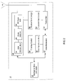
- the transmitter system 70 includes a data modulation unit 20 coupled to a transmitter 16 , a transmit gain control unit 21 which is also coupled to transmitter 16 , and an antenna 14 which receives signals from transmitter 16 for transmission via antenna 14 .
- the data modulation unit 20 further comprises a pulse amplitude modulation module 72 , a pulse repetition frequency module 74 and a transmit module 76 .
- the pulse repetition frequency module is configured to provide a variable pulse repetition frequency to transmitter system 70 .
- the pulse amplitude modulation module is configured to provide modulation techniques in which the amplitude for pulses may be varied depending on the value represented by the pulse amplitude modulated pulse.
- the transmit module 76 is in direct communication with pulse amplitude module 72 and pulse repetition frequency module 74 .
- the pulse amplitude modulation module 72 is coupled to amplitude control system 75 .
- the pulse amplitude modulation module 72 , amplitude control system 75 , and the pulse repetition frequency module 74 are described in further detail below.
- data modulation unit 20 is configured to generate a digital stream of pulse data.
- the digital stream of pulse data generated by the data modulation unit 20 includes a transmit module configured to generate a clock pulse and pulse amplitude modulation module configured to generate a data stream for a desired pulse amplitude.
- the transmit module 76 provides the ability to distinguish between different modulation techniques such as pulse amplitude modulation (PAM) and on-off keying (OOK). If the transmit module detects that a signal is modulated by OOK, the OOK signal is communicated directly to the transmitter 16 . If the transmit module detects that a signal is modulated by PAM, then the transmit signal is communicated to the PAM module 72 .
- PAM pulse amplitude modulation
- OOK on-off keying
- the transmit module 76 communicates with a pulse repetition frequency module 72 .
- the transmit pulses are digital clock pulses which are communicated at the particular pulse repetition frequency.
- the pulse repetition frequency module 72 performs the function of varying the pulse repetition frequency and the corresponding bit rate for communications. The bit rate is varied depending on environmental and network demands. Another benefit provided by the pulse repetition frequency module 72 is to reduce the amount of interference generated by the baseband transmitter by periodically modifying the pulse repetition rate of the baseband transmitter.
- the transmit module 76 generates the transmit pulse signals which are communicated to the transmitter 16 pulse generator system 78 .
- the transmit pulses are digital clock pulses which are communicated at a particular pulse repetition frequency. Additionally, the transmit module 76 provides the ability to distinguish between different modulation techniques such as pulse amplitude modulation (PAM) and on-off keying (OOK). If the transmit module detects that a signal is modulated by OOK, the OOK signal is communicated directly to the transistor drive system 79 . If the transmit module detects that a signal is modulated by PAM, then the transmit signal is communicated to the PAM module 72 .
- PAM pulse amplitude modulation
- OOK on-off keying
- the modulation technique for the pulse stream generated by the data modulator 20 is synchronized with the master clock 13 associated with the clock synchronization unit 34 , and is sent in an appropriate time slot according to a frame definition provided by the framing control unit 32 .
- one device To maintain a synchronized network, one device must serve the function of being a clock master and maintaining the master clock 13 for the network 10 .
- the amplitude control system 75 receives data signals from the pulse amplitude module 72 in which the data signals provide data about the desired pulse amplitude to be generated by the amplitude control system 75 .
- Two illustrative amplitude control systems described in further detail below include a variable gain amplifier and an attenuator.
- the pull-up circuits and pull-down circuits also include a pulse generator system 78 .
- the pulse generator system includes four pulse generators 80 , 82 , 84 and 86 .
- the pulse generating system 78 presents the rising edge of an input transmit pulse 88 to the one or more pulse generators.
- the pulse generator system generates output signals that are presented to the drive system as pull-up turn-on signals 90 , pull-up turn-off signals 92 , pull-down turn-on signals 94 , and pull-down turn-off signals 96 .
- each typical pulse generator includes four pairs of coupled edge delay circuits which are coupled to one another.
- pulse generator 80 includes edge delay circuits 98 through 112 , which function in pairs.
- the pulse generator 80 is composed of four (4) pairs of edge delay circuits in which each pair of edge delay circuit includes an edge delay circuit that generates a leading edge and another edge delay circuit that generates a trailing edge.
- the first pair of edge delay circuits in pulse generator 80 include a first edge delay circuit 98 which generates the leading edge for the delayed pulse signal and the second edge delay circuit 100 which generates the trailing edge for the delayed pulse signal.
- each pair of edge delay circuits generates the leading and trailing edges for each delayed pulse signal. More particularly, each edge delay circuit may comprise a switched bank of capacitors that provide a programmable edge delay. It shall be appreciated by those skilled in the art having the benefit of this disclosure that the outputs from each pair of edge delay circuits are combined to produce a composite series of delayed output pulses for pulse generator 80 . Each of the remaining pulse generators 82 , 84 and 86 also each generate a composite series of delayed output pulses.
- the delayed output pulses from pulse generators 80 , 82 , 84 and 86 are presented as pull-up turn-on signals 90 (identified as Pon), pull-up turn-off signals 92 (identified as Poff), pull-down turn-on signals 94 (identified as Non), and pull-down turn-off signals 96 (identified as Noff) to the drive system 79 .
- the drive system 79 combines these pull-up turn-on signals 90 , pull-up turn-off signals 92 , pull-down turn-on signals 94 , and pull-down turn-off signals 96 to generate a waveform which is communicated to antenna 14 .
- the pull-down circuit which generates the negative going signals excursion includes a bipolar npn transistor 124 .
- the npn transistor 124 is a pull-down transistor in a common emitter configuration that receives the pull down signals at its base 126 .
- the pull-down signals are a combination of the Poff signals 92 and the Non signals 94 .
- the outputs from the bipolar transistors are capacitively coupled to the load 128 .
- the method 150 includes a process 50 in which input transmit pulse 88 for transmission is communicated to pulse generator system 78 .
- the pulse generator system 78 comprises a plurality of pulse generators 82 , 82 , 84 and 86 which produce pull-up turn-on signals 90 (identified as Pon), pull-up turn-off signals 92 (identified as Poff), pull-down turn-on signals 94 (identified as Non), and pull-down turn-off signals 96 (identified as Noff), respectively.
- the positive signal excursions are generated preferably by a bipolar pnp transistor 120 .
- the pnp transistor is a pull-up transistor in a common emitter configuration that receives the pull-up signals at its base 122 .
- the pull-up signals are a combination of the pull-up turn on (Pon) signals 90 and the pull down turn off signals (Noff) 96 .
- the method then proceeds to process 156 .
- negative signal excursions are generated by a pull-down circuit.
- the pull-down circuit which generates the negative going signal excursion includes a bipolar npn transistor 124 .
- the npn transistor 124 is a pull-down transistor in a common emitter configuration the receives the pull down signals at its base 126 .
- the pull down signals are a combination of the pull-up turn off (Poff) signals 92 and the pull-down turn-on (Non) signals 94 .
- the method then proceeds to process 158 .
- the positive and negative signal excursions are combined to generate a base band signal.
- the positive and negative signal excursions are combined and amplified by the drive system 79 to generate a RF pulse stream. The method then proceeds to process 160 .
- the RF pulse stream from process 158 is communicated to an antenna 14 for transmission.
- the RF pulse stream is a baseband signal is a doublet as shouwn in FIG. 6 b.
- FIG. 7 there is shown a block diagram of a pulse repetition frequency module and pulse amplitude modulation module which is resident on the Medium Access Control (MAC) 170 layer of the transmitter of the present invention.
- the MAC 170 is provided at the Data Link Layer, which is located between the Network Layer and Physical Layer of the OSI reference model.
- the MAC 170 of the present invention provides the circuitry for varying the pulse repetition frequency.
- the MAC 170 comprises an integrated circuit or like hardware device providing the functions described herein. It shall be appreciated by those skilled in the art that some MAC services may be implemented in software.
- the MAC functions implemented herein refer to those MAC functions implemented in hardware that are unique to the present invention.
- the MAC hardware includes a clock synchronization function 34 ( FIG. 2 ) which is coupled to a plurality of frequency dividers 174 , 176 , 178 and 180 in which each frequency divider is configured to divide down the clock speed.
- a plurality of slot allocation units 182 , 184 , 186 and 188 having different pulse repetition frequencies and different modulation techniques are each coupled to frequency dividers 174 , 176 , 178 and 180 , respectively.
- Each slot allocation unit 182 through 188 is operatively coupled to a multiplexer/demultiplexer unit 190 which is operatively coupled to an interface to the Physical Layer 192 .
- the clock sync function 34 is configured to synchronize a local clock on the transmitter to the master transceiver 12 a clock 13 .
- the clock sync function 34 produces a high speed clock that is a multiple of the highest pulse repetition frequency supported by the transmitter of the present invention.
- Each programmable frequency divider 174 through 180 is capable of generating a varying pulse repetition frequency by dividing down the high-speed clock associated with the clock sync function 34 .
- Each slot allocation unit 182 through 188 may have a different pulse repetition frequency and different modulation technique.
- each slot allocation unit 182 through 188 also has a common undivided clock (not shown) to serve as reference for counting out the start location of each slot based on a uniform time base.
- each slot allocation unit 182 through 188 is programmed to provide a symbol stream to the physical layer and transmit data pulses and clocking information at the appropriate pulse repetition frequency.
- each slot allocation unit 182 through 188 provides data in the appropriate data width to support different modulation techniques.
- data will be supplied at a rate of one-bit per clock cycle.
- the modulation technique provides for two bits to be communicated per clock cycle.
- the modulation technique provides for three bits to be communicated per clock cycle.
- each slot allocation unit has an associated start time, length, and modulation technique.
- the slot allocation unit will take over control the physical layer through communications with multiplexor/demultiplexor 190 .
- Each slot allocation unit provides data signals having the proper width and proper pulse repetition frequency in the form of data control and clock.
- the slot allocation unit relinquishes control and the following slot allocation unit has the opportunity to take control during its respective designated transmit time.
- the data and clock information supplied by the MAC 170 to the physical layer will be fed to the pulse generation system 78 and the drive system 79 which will generate the proper waveform at the appropriate time and amplitude.
- the Mux/Demux 190 carries out the operation of merging outgoing bit streams from slot allocation units 182 through 188 into a single signal transmitted to the transmit module 76 and then to pulse generating system 78 and drive system 79 .
- FIG. 8 a there is show n a block diagram of one embodiment of an amplitude control system having a variable gain amplifier 204 .
- a transmit module which generates a clock pulse at the proper time, communicates the clock pulse to the pulse generator system 78 of the transmitter 16 .
- the output from pulse generator system 78 is submitted to a drive system 79 which generates a RF pulse stream that is communicated to a variable gain amplifier 204 .
- the variable gain amplifier 204 is operatively coupled to the transmitting antenna 14 .
- a pulse amplitude modulation module 72 is coupled to the variable gain amplifier 204 .
- the variable gain amplifier 204 amplifies the pulse generated by the drive system 79 .
- the pulse generator system 78 is supplied with a clock or strobe signal from transmit module 76 .
- the transmit module 76 generates a clock pulse which is communicated to the pulse generator system 78 .
- the pulse amplitude modulation module 72 is configured to generate a data stream which is communicated to the amplitude control system having a variable gain amplifier 204 .
- the output from the drive system 79 is submitted to the variable gain amplifier 204 which provides the requisite gain to generate an RF pulse for transmission by antenna 14 having the desired amplitude.
- FIG. 8 b there is shown an alternative block diagram of another amplitude control system having an attenuator 214 .
- a transmit module which generates a clock pulse at the proper time, communicates the clock pulse to pulse generator system 78 .
- the output from pulse generator 78 is submitted to a drive system 79 which generates a RF pulse stream at a maximum amplitude.
- the maximum amplitude output from the drive system 79 is communicated to a digitally controlled attenuator 214 which is coupled to antenna 14 .
- a pulse amplitude modulation module 72 is coupled to the attenuator 214 which attenuates the waveform generated by the drive system 79 .
- the attenuator 214 reduces the amplitude of the waveform as needed to provide the correct signal for transmission by antenna 14 .
- the pulse generator system 78 is supplied with a clock or strobe signal from transmit module 76 .
- the transmit module 76 generates a clock pulse which is communicated to the pulse generator system 78 .
- the pulse amplitude modulation module 72 is configured to generate a data stream which is communicated to the amplitude control system having an attenuator 214 .
- the output from the drive system 79 is then submitted to attenuator 214 which reduces the amplitude of the RF pulses according to the output generated by the data interface 216 .
- the present invention is configured to employ various pulse repetition frequencies and various modulation techniques.
- the slot allocation unit e.g. slot allocation unit 184
- the modulation technique to be employed. If the modulation technique is on-off keying, the data interface for the pulse amplitude modulation module 72 will be disabled, and the amplifier 206 or attenuater 214 will be set to a fixed value, typically full power.
- the data interface for the pulse amplitude modulation module 72 will be enabled to support the number of bits used for pulse amplitude modulation. For example if the transmitter supports both four (4) level pulse amplitude modulation (2 bits) and eight (8) level pulse amplitude modulation (3 bits), either, two or three bits of the digital interface are enabled.
- the data interface will typically be tied to logic ‘1’, so that symbols 001, 011, 101 and 111 are used for the four (4) level pulse amplitude modulated signals.
- the pulse amplitude modulation unit may be reconfigured to ignore one bit of the three bit value and generate four equally spaced voltage outputs representing the symbols 00, 01, 10, and 11. It shall be appreciated by those skilled in the art that there are other alternatives for the illustrative four symbols.
- a first typical TDMA slot 220 and second typical TDMA slot 222 provides communications within a data slot.
- the master sync code synchronizes communications between transceiver devices using a clock synchronization unit 34 operating at a nominal pulse repetition frequency that the system 10 will support.
- the transmitter 16 and receiver 18 are capable of frequency multiplying the clock from the clock synchronization unit 34 to support higher pulse repetition frequencies.
- the pulse repetition frequencies employed may depend on the devices particular bandwidth demands, noise constraints, or signal reflection.
- Client bit clock — 1 , 224 provides the timing for the pulse repetition frequency associated with TDMA Slot N+ 1 , 222 .
- the signals transmitted by TDMA slot 222 are transmitted during the leading edge of client bit clock — 1 , 224 .
- Client bit clock — 2 226 provides the timing for the pulse repetition frequency associated with TDMA slot N 220 .
- the signals transmitted by TDMA Slot N 220 are transmitted during the leading edge of client bit clock — 2 226 .
- the pulse repetition frequency for TDMA Slot N, 220 is two times greater, i.e. faster, that the pulse repetition frequency for TDMA Slot N+ 1 , 222 .
- the pulse repetition frequency for TDMA Slot N, 220 , and TDMA Slot N+ 1 , 222 is identified by the frequency pulses, identified by arrows, shown in line 228 .
- a client bit clock 230 provides the timing for the two typical TDMA slot in the data slot section of TDMA frame.
- the two typical TDMA frames are identified as TDMA Slot N, 232 , and TDMA Slot N+ 1 , 234 .
- the signal transmitted employs pulse amplitude modulation as depicted by the symbols in line 236 .
- the timing for each of the pulses having a different amplitude is established by the client bit clock 230 .
- TDMA Slot N+ 1 234 the signal transmitted employs on-off keying as depicted by the symbols in line 236 . Again, the timing for each of the pulses operating with on-off keying is established by the client bit clock 230 .
- pulse-position modulation uses different bit pulse repetition frequencies and modulation techniques for baseband communications or ultra-wide-band communications.
- pulse-position modulation is well known in the art and may also be employed with the present system and method.
- pulses are transmitted at some basic symbol frequency, e.g. 20 MHz. At a 20 MHz symbol repetition frequency that pulses are spaced 50 nanoseconds apart. A pulse falling exactly where expected may indicate a binary “1”, while a pulse delayed by some small delta time may indicate a binary “0”.
Abstract
Description
Claims (6)
Priority Applications (8)
| Application Number | Priority Date | Filing Date | Title |
|---|---|---|---|
| US09/599,969 US6952456B1 (en) | 2000-06-21 | 2000-06-21 | Ultra wide band transmitter |
| DE60128225T DE60128225T2 (en) | 2000-06-21 | 2001-06-21 | ULTRA BROADBAND CHANNEL |
| AU2001268664A AU2001268664A1 (en) | 2000-06-21 | 2001-06-21 | Ultra wide band transmitter |
| PCT/US2001/019908 WO2001099305A2 (en) | 2000-06-21 | 2001-06-21 | Ultra wide band transmitter |
| AT01946645T ATE361614T1 (en) | 2000-06-21 | 2001-06-21 | ULTRA WIDE BAND TRANSMITTER |
| EP01946645A EP1295450B1 (en) | 2000-06-21 | 2001-06-21 | Ultra wide band transmitter |
| ES01946645T ES2284658T3 (en) | 2000-06-21 | 2001-06-21 | ULTRA WIDE BAND TRANSMITTER. |
| US10/820,348 US20040190666A1 (en) | 2000-06-21 | 2004-04-07 | Ultra wide band transmitter |
Applications Claiming Priority (2)
| Application Number | Priority Date | Filing Date | Title |
|---|---|---|---|
| US09/599,969 US6952456B1 (en) | 2000-06-21 | 2000-06-21 | Ultra wide band transmitter |
| PCT/US2001/019908 WO2001099305A2 (en) | 2000-06-21 | 2001-06-21 | Ultra wide band transmitter |
Related Parent Applications (1)
| Application Number | Title | Priority Date | Filing Date |
|---|---|---|---|
| PCT/US2001/019908 Continuation WO2001099305A2 (en) | 2000-06-21 | 2001-06-21 | Ultra wide band transmitter |
Related Child Applications (1)
| Application Number | Title | Priority Date | Filing Date |
|---|---|---|---|
| US10/820,348 Division US20040190666A1 (en) | 2000-06-21 | 2004-04-07 | Ultra wide band transmitter |
Publications (1)
| Publication Number | Publication Date |
|---|---|
| US6952456B1 true US6952456B1 (en) | 2005-10-04 |
Family
ID=24401858
Family Applications (2)
| Application Number | Title | Priority Date | Filing Date |
|---|---|---|---|
| US09/599,969 Expired - Fee Related US6952456B1 (en) | 2000-06-21 | 2000-06-21 | Ultra wide band transmitter |
| US10/820,348 Abandoned US20040190666A1 (en) | 2000-06-21 | 2004-04-07 | Ultra wide band transmitter |
Family Applications After (1)
| Application Number | Title | Priority Date | Filing Date |
|---|---|---|---|
| US10/820,348 Abandoned US20040190666A1 (en) | 2000-06-21 | 2004-04-07 | Ultra wide band transmitter |
Country Status (7)
| Country | Link |
|---|---|
| US (2) | US6952456B1 (en) |
| EP (1) | EP1295450B1 (en) |
| AT (1) | ATE361614T1 (en) |
| AU (1) | AU2001268664A1 (en) |
| DE (1) | DE60128225T2 (en) |
| ES (1) | ES2284658T3 (en) |
| WO (1) | WO2001099305A2 (en) |
Cited By (35)
| Publication number | Priority date | Publication date | Assignee | Title |
|---|---|---|---|---|
| US20030035465A1 (en) * | 2001-08-17 | 2003-02-20 | Kazuhisa Takamura | Radio communications system, transmitter, receiver, radio transmission method, radio reception method and computer program therefor |
| US20030128720A1 (en) * | 2002-01-09 | 2003-07-10 | Jones Delon K. | Method and apparatus for aligning the clock signals of transceivers in a multiple access communication system utilizing programmable, multi-tap phase-locked loops |
| US20030198212A1 (en) * | 2002-04-19 | 2003-10-23 | General Electric Company | Method and apparatus for synchronizing a radio telemetry system by way of transmitted-reference , delay-hopped ultra-wideband pilot signal |
| US20040008641A1 (en) * | 2002-04-15 | 2004-01-15 | Sony Corporation | Communications system, communications control apparatus and method, and computer program therefor |
| US20040032354A1 (en) * | 2002-08-16 | 2004-02-19 | Yaron Knobel | Multi-band ultra-wide band communication method and system |
| US20040077306A1 (en) * | 2002-08-16 | 2004-04-22 | Gadi Shor | Scalable ultra-wide band communication system |
| US20040125859A1 (en) * | 2002-12-31 | 2004-07-01 | Evan Green | Method and apparatus to generate a clock-based transmission |
| US20040131130A1 (en) * | 2002-08-16 | 2004-07-08 | Gadi Shor | System and method for multi-band ultra-wide band signal generators |
| US20050041725A1 (en) * | 2003-05-26 | 2005-02-24 | Commissariat A L'energie Atomique | Receiver of an ultra wide band signal and associated reception method |
| US20050047367A1 (en) * | 2001-12-06 | 2005-03-03 | Ismail Lakkis | Ultra-wideband communication systems and methods |
| US20050068932A1 (en) * | 2000-09-25 | 2005-03-31 | Ismail Lakkis | Ultra-wideband communication system and methods |
| US20050124293A1 (en) * | 2003-12-04 | 2005-06-09 | Alicherry Mansoor A.K. | Method and apparatus for mobile telephone locatability |
| US20050221760A1 (en) * | 2004-03-31 | 2005-10-06 | Tinsley Keith R | Pulse shaping signals for ultrawideband communication |
| US20050237965A1 (en) * | 2004-01-08 | 2005-10-27 | Yefim Kuperschmidt | Method and devices for multicasting information over a network that applied a distributed media access control scheme |
| US20060114879A1 (en) * | 2004-11-30 | 2006-06-01 | Freescale Semiconductor Inc. | Method for sharing bandwidth using reduced duty cycle signals |
| US20060164271A1 (en) * | 2003-03-12 | 2006-07-27 | Walter Hirt | Method and apparatus for converting optical signals to radio channels |
| US20060197618A1 (en) * | 2005-02-18 | 2006-09-07 | Renesas Technology Corp. | Pulse generator and the transmitter with a pulse generator |
| US20060199620A1 (en) * | 2005-02-24 | 2006-09-07 | Firefly Power Technologies, Inc. | Method, apparatus and system for power transmission |
| US20060209769A1 (en) * | 2004-02-05 | 2006-09-21 | Shigeo Akamatsu | Jitter correcting apparatus capable of ensuring synchronism between transmitter apparatus and receiver apparatus |
| US20070149162A1 (en) * | 2005-02-24 | 2007-06-28 | Powercast, Llc | Pulse transmission method |
| US20070147476A1 (en) * | 2004-01-08 | 2007-06-28 | Institut De Microtechnique Université De Neuchâtel | Wireless data communication method via ultra-wide band encoded data signals, and receiver device for implementing the same |
| US20070153875A1 (en) * | 2003-03-03 | 2007-07-05 | Ismail Lakkis | Ultra-wideband pulse modulation system and method |
| WO2007081971A2 (en) * | 2006-01-11 | 2007-07-19 | Powercast Corporation | Pulse transmission method |
| US20070248114A1 (en) * | 2006-04-20 | 2007-10-25 | Qualcomm Incorporated | Media access control for ultra-wide band communication |
| US20080080547A1 (en) * | 2006-09-29 | 2008-04-03 | Motorola, Inc. | System and method for forming a time division multiple access frame in a simulcast system |
| US20080151792A1 (en) * | 2006-12-22 | 2008-06-26 | Teranetics, Inc. | Aiding synchronization between master and slave transceivers |
| US20100130144A1 (en) * | 2008-11-24 | 2010-05-27 | Qualcomm Incorporated | Techniques for improving transmitter performance |
| US20100190517A1 (en) * | 2007-08-03 | 2010-07-29 | Cornell University | Pulse coupled oscillator synchronization for wireless communications |
| US7929596B2 (en) | 2001-12-06 | 2011-04-19 | Pulse-Link, Inc. | Ultra-wideband communication apparatus and methods |
| US20110255449A1 (en) * | 2003-08-22 | 2011-10-20 | Rappaport Theodore S | Broadband Repeater with Security for Ultrawideband Technologies |
| US8045935B2 (en) | 2001-12-06 | 2011-10-25 | Pulse-Link, Inc. | High data rate transmitter and receiver |
| US8351483B1 (en) * | 2006-12-18 | 2013-01-08 | University Of South Florida | Architecture for ultra-wideband radio |
| US20140217967A1 (en) * | 2013-02-04 | 2014-08-07 | Ossia, Inc. | Systems and methods for optimally delivering pulsed wireless power |
| US9685711B2 (en) | 2013-02-04 | 2017-06-20 | Ossia Inc. | High dielectric antenna array |
| US11706707B2 (en) | 2014-01-09 | 2023-07-18 | Transfert Plus, Société En Commandite | Methods and systems relating to ultra wideband transmitters |
Families Citing this family (11)
| Publication number | Priority date | Publication date | Assignee | Title |
|---|---|---|---|---|
| US7023833B1 (en) | 1999-09-10 | 2006-04-04 | Pulse-Link, Inc. | Baseband wireless network for isochronous communication |
| AU2001271297A1 (en) * | 2000-06-12 | 2001-12-24 | Larry W. Fullerton | A method for specifying non-temporal pulse characteristics |
| US6911874B2 (en) * | 2002-02-04 | 2005-06-28 | Honeywell International Inc. | Ultra-wideband impulse generation and modulation circuit |
| US7570627B2 (en) * | 2005-03-11 | 2009-08-04 | Freescale Semiconductor, Inc. | Method for sharing bandwidth using reduced duty cycle signals and media access control |
| US8866347B2 (en) | 2010-01-15 | 2014-10-21 | Idex Asa | Biometric image sensing |
| FR2963512B1 (en) * | 2010-07-27 | 2012-08-17 | Univ Provence Aix Marseille 1 | METHOD AND DEVICE FOR GENERATING ULTRA BROADBAND (UWB) PULSES |
| WO2015081412A1 (en) * | 2013-12-03 | 2015-06-11 | Smart Energy Instruments Inc. | Communication systems and methods for distributed power system measurement |
| EP3584601B1 (en) * | 2018-06-18 | 2023-10-18 | NXP USA, Inc. | Time-encoded messaging for radar cascaded synchronization system |
| EP3591432B1 (en) * | 2018-07-02 | 2021-06-30 | NXP USA, Inc. | Communication unit, integrated circuit and method for clock distribution and synchronization |
| EP3591431B1 (en) * | 2018-07-02 | 2021-05-05 | NXP USA, Inc. | Communication unit and method for clock distribution and synchronization |
| EP3591433B1 (en) | 2018-07-02 | 2023-06-14 | NXP USA, Inc. | Communication unit, integrated circuits and method for clock and data synchronization |
Citations (103)
| Publication number | Priority date | Publication date | Assignee | Title |
|---|---|---|---|---|
| US3668639A (en) | 1971-05-07 | 1972-06-06 | Itt | Sequency filters based on walsh functions for signals with three space variables |
| US3678204A (en) | 1970-10-26 | 1972-07-18 | Itt | Signal processing and transmission by means of walsh functions |
| US3728632A (en) | 1971-03-12 | 1973-04-17 | Sperry Rand Corp | Transmission and reception system for generating and receiving base-band pulse duration pulse signals without distortion for short base-band communication system |
| US3875524A (en) | 1972-08-16 | 1975-04-01 | Wandel & Goltermann | Phase-stable decadically adjustable frequency synthesizer |
| US4232339A (en) | 1978-09-08 | 1980-11-04 | Harris Corporation | Television signal horizontal interval timing reconstruction system |
| US4506267A (en) | 1983-01-26 | 1985-03-19 | Geophysical Survey Systems, Inc. | Frequency independent shielded loop antenna |
| US4574378A (en) | 1982-06-14 | 1986-03-04 | Nec Corporation | Multiple access system and method |
| US4641317A (en) | 1984-12-03 | 1987-02-03 | Charles A. Phillips | Spread spectrum radio transmission system |
| US4644534A (en) | 1984-07-03 | 1987-02-17 | Ant Nachrichtentechnik Gmbh | TDMA point-to-multipoint communications system and its use |
| US4651152A (en) | 1983-09-26 | 1987-03-17 | Geophysical Survey Systems, Inc. | Large relative bandwidth radar |
| US4672608A (en) | 1984-09-26 | 1987-06-09 | U.S. Philips Corporation | Multiple access communications system |
| US4743906A (en) | 1984-12-03 | 1988-05-10 | Charles A. Phillips | Time domain radio transmission system |
| US4763325A (en) | 1985-09-04 | 1988-08-09 | Comsat Telesystems, Inc. | Demand assigned reformatting with an overflow area for time division multiple access communication |
| US4813057A (en) | 1984-12-03 | 1989-03-14 | Charles A. Phillips | Time domain radio transmission system |
| EP0307962A2 (en) | 1987-09-21 | 1989-03-22 | Nec Corporation | Time division multiple access radio communication system |
| US5134408A (en) | 1991-01-30 | 1992-07-28 | Geophysical Survey Systems, Inc. | Detection of radar signals with large radar signatures |
| US5146616A (en) * | 1991-06-27 | 1992-09-08 | Hughes Aircraft Company | Ultra wideband radar transmitter employing synthesized short pulses |
| US5148174A (en) | 1991-02-13 | 1992-09-15 | Geophysical Survey Systems, Inc. | Selective reception of carrier-free radar signals with large relative bandwidth |
| US5153595A (en) | 1990-03-26 | 1992-10-06 | Geophysical Survey Systems, Inc. | Range information from signal distortions |
| US5159343A (en) | 1990-03-26 | 1992-10-27 | Geophysical Survey Systems, Inc. | Range information from signal distortions |
| US5307081A (en) | 1990-11-27 | 1994-04-26 | Geophysical Survey Systems, Inc. | Radiator for slowly varying electromagnetic waves |
| US5334975A (en) | 1991-07-16 | 1994-08-02 | Wachob David E | Residential time reference system |
| US5365240A (en) | 1992-11-04 | 1994-11-15 | Geophysical Survey Systems, Inc. | Efficient driving circuit for large-current radiator |
| US5493691A (en) | 1993-12-23 | 1996-02-20 | Barrett; Terence W. | Oscillator-shuttle-circuit (OSC) networks for conditioning energy in higher-order symmetry algebraic topological forms and RF phase conjugation |
| US5519400A (en) * | 1993-04-12 | 1996-05-21 | The Regents Of The University Of California | Phase coded, micro-power impulse radar motion sensor |
| US5523758A (en) | 1990-01-25 | 1996-06-04 | Geophysical Survey Systems, Inc. | Sliding correlator for nanosecond pulses |
| US5586145A (en) | 1993-01-11 | 1996-12-17 | Morgan; Harry C. | Transmission of electronic information by pulse position modulation utilizing low average power |
| US5592177A (en) | 1993-06-11 | 1997-01-07 | Autometric, Incorporated | Polarization-rotation modulated, spread polarization-rotation, wide-bandwidth radio-wave communications system |
| US5594738A (en) | 1993-10-18 | 1997-01-14 | Motorola, Inc. | Time slot allocation method |
| US5610907A (en) | 1994-07-29 | 1997-03-11 | Barrett; Terence W. | Ultrafast time hopping CDMA-RF communications: code-as-carrier, multichannel operation, high data rate operation and data rate on demand |
| US5644576A (en) * | 1994-10-26 | 1997-07-01 | International Business Machines Corporation | Medium access control scheme for wireless LAN using a variable length interleaved time division frame |
| US5675388A (en) | 1982-06-24 | 1997-10-07 | Cooper; J. Carl | Apparatus and method for transmitting audio signals as part of a television video signal |
| US5677927A (en) * | 1994-09-20 | 1997-10-14 | Pulson Communications Corporation | Ultrawide-band communication system and method |
| US5687169A (en) * | 1995-04-27 | 1997-11-11 | Time Domain Systems, Inc. | Full duplex ultrawide-band communication system and method |
| EP0817399A2 (en) | 1990-06-05 | 1998-01-07 | Siemens Measurements Limited | Polling in a mains metering system |
| US5715236A (en) | 1990-06-25 | 1998-02-03 | Qualcomm Incorporated | System and method for generating signal waveforms in a CDMA cellular telephone system |
| EP0825794A2 (en) | 1996-08-21 | 1998-02-25 | Lucent Technologies Inc. | A network flow framework for online dynamic channel allocation |
| US5748891A (en) | 1994-07-22 | 1998-05-05 | Aether Wire & Location | Spread spectrum localizers |
| US5761197A (en) | 1994-11-14 | 1998-06-02 | Northern Telecom Limited | Communications in a distribution network |
| US5812671A (en) | 1996-07-17 | 1998-09-22 | Xante Corporation | Cryptographic communication system |
| US5832035A (en) * | 1994-09-20 | 1998-11-03 | Time Domain Corporation | Fast locking mechanism for channelized ultrawide-band communications |
| US5850422A (en) | 1995-07-21 | 1998-12-15 | Symbios, Inc. | Apparatus and method for recovering a clock signal which is embedded in an incoming data stream |
| US5886652A (en) | 1995-08-03 | 1999-03-23 | Ntt Mobile Communications Network, Inc. | Pseudo fixed data transmission device and method |
| US5889767A (en) | 1994-08-29 | 1999-03-30 | Nec Corporation | Time-division multidirectional multiplex communication system capable of using message area in radio burst signals divided into a plurality of areas |
| US5903605A (en) | 1995-03-30 | 1999-05-11 | Intel Corporation | Jitter detection method and apparatus |
| US5909491A (en) | 1996-11-06 | 1999-06-01 | Nokia Mobile Phones Limited | Method for sending a secure message in a telecommunications system |
| US5920278A (en) | 1997-05-28 | 1999-07-06 | Gregory D. Gibbons | Method and apparatus for identifying, locating, tracking, or communicating with remote objects |
| US5940435A (en) | 1996-11-21 | 1999-08-17 | Dsp Group, Inc. | Method for compensating filtering delays in a spread-spectrum receiver |
| US6026125A (en) * | 1997-05-16 | 2000-02-15 | Multispectral Solutions, Inc. | Waveform adaptive ultra-wideband transmitter |
| US6041051A (en) | 1996-06-14 | 2000-03-21 | Lucent Technologies, Inc. | Method and apparatus enabling multiple access for multiple services and multiple transmission modes over a broadband communication network utilizing an adaptive digital access protocol |
| US6064697A (en) | 1995-10-30 | 2000-05-16 | Smk Corporation | Pulse modulating method, pulse modulating equipment and pulse demodulating equipment |
| US6067648A (en) | 1998-03-02 | 2000-05-23 | Tanisys Technology, Inc. | Programmable pulse generator |
| US6069887A (en) | 1997-05-28 | 2000-05-30 | Apple Computer, Inc. | Method and system for synchronization in a wireless local area network |
| US6097766A (en) | 1997-10-30 | 2000-08-01 | Mitsubishi Denki Kabushiki Kaisha | Timing phase synchronization detecting circuit and demodulator |
| US6122291A (en) | 1996-03-07 | 2000-09-19 | Motorola, Inc. | Communication system and operating method thereof |
| US6133876A (en) | 1998-03-23 | 2000-10-17 | Time Domain Corporation | System and method for position determination by impulse radio |
| US6133875A (en) | 1996-10-16 | 2000-10-17 | Nikon Corporation | Position determining apparatus and position determining method using the same |
| US6161138A (en) | 1996-04-12 | 2000-12-12 | Peak Audio, Inc. | Media access control for isochronous data packets in carrier sensing multiple access systems |
| US6172965B1 (en) | 1996-12-23 | 2001-01-09 | Nortel Networks Limited | Duplex transmission scheme |
| US6177903B1 (en) | 1999-06-14 | 2001-01-23 | Time Domain Corporation | System and method for intrusion detection using a time domain radar array |
| US6178217B1 (en) | 1994-08-12 | 2001-01-23 | Neosoft, A.G. | Nonlinear digital communications system |
| US6181687B1 (en) | 1998-10-22 | 2001-01-30 | International Business Machines Corporation | System and a method for continuously adjustable, splitting group, multi-contention resolution in multi-access computer communication systems |
| US6212230B1 (en) | 1998-04-04 | 2001-04-03 | Sigmatel, Inc. | Method and apparatus for pulse position modulation |
| US6232910B1 (en) | 1998-02-20 | 2001-05-15 | Amerigon, Inc. | High performance vehicle radar system |
| US6236662B1 (en) | 1998-05-04 | 2001-05-22 | Bae Systems Aerospace Inc. | Multirate time reservation multi-access protocol |
| US6239741B1 (en) * | 1998-07-20 | 2001-05-29 | Multispectral Solutions, Inc. | UWB dual tunnel diode detector for object detection, measurement, or avoidance |
| US6246277B1 (en) | 1997-12-26 | 2001-06-12 | Hitachi, Ltd. | Semiconductor integrated circuit device |
| US6275500B1 (en) | 1999-08-09 | 2001-08-14 | Motorola, Inc. | Method and apparatus for dynamic control of talk groups in a wireless network |
| US6292153B1 (en) | 1999-08-27 | 2001-09-18 | Fantasma Network, Inc. | Antenna comprising two wideband notch regions on one coplanar substrate |
| US6310865B1 (en) | 1997-06-20 | 2001-10-30 | Nec Corporation | High-speed wireless access device |
| US6324397B1 (en) | 1996-03-27 | 2001-11-27 | Aiwa Co., Ltd. | Portable terminal equipment |
| US20010055353A1 (en) | 1998-04-04 | 2001-12-27 | Mathew A. Rybicki | Method and apparatus for amplitude and pulse modulation |
| US20020018458A1 (en) | 1999-09-10 | 2002-02-14 | Fantasma Network, Inc. | Baseband wireless network for isochronous communication |
| US6351652B1 (en) | 1999-10-26 | 2002-02-26 | Time Domain Corporation | Mobile communications system and method utilizing impulse radio |
| US6351468B1 (en) | 1998-07-02 | 2002-02-26 | Gte Service Corporation | Communications protocol in a wireless personal area network |
| US6385461B1 (en) | 1998-11-16 | 2002-05-07 | Ericsson Inc. | User group indication and status change in radiocommunications systems |
| US6400308B1 (en) | 1998-02-20 | 2002-06-04 | Amerigon Inc. | High performance vehicle radar system |
| US6424645B1 (en) | 1998-09-09 | 2002-07-23 | Mitsubishi Denki Kabushiki Kaisha | TDMA radio communication system achieving simultaneous assignment of channels to multiple terminal stations |
| US6437832B1 (en) | 1999-10-21 | 2002-08-20 | General Electric Company | Mitigation of multipath using ultra wideband DTV overlay signal |
| US6449265B1 (en) | 1999-01-15 | 2002-09-10 | Trw Inc. | Media access control layer for satellite ATM networks |
| US20020131370A1 (en) | 2000-12-19 | 2002-09-19 | Chuah Mooi Choo | Clock offset estimation with bias correction |
| US6463042B1 (en) | 1999-05-28 | 2002-10-08 | Nokia Mobile Phones Ltd. | Mobile station having power saving mode for packet data |
| US6477171B1 (en) | 1999-12-01 | 2002-11-05 | Agilent Technologies, Inc. | Method and system for negotiation of the highest common link rate among nodes of a fibre channel arbitrated loop |
| US6480505B1 (en) | 1999-12-06 | 2002-11-12 | Telefonaktiebolaget Lm Ericsson (Publ) | Batched fair exhaustive polling scheduler |
| US6492904B2 (en) | 1999-09-27 | 2002-12-10 | Time Domain Corporation | Method and system for coordinating timing among ultrawideband transmissions |
| US6497656B1 (en) | 2000-02-08 | 2002-12-24 | General Electric Company | Integrated wireless broadband communications network |
| US6505032B1 (en) | 2000-05-26 | 2003-01-07 | Xtremespectrum, Inc. | Carrierless ultra wideband wireless signals for conveying application data |
| US6510150B1 (en) | 1998-12-21 | 2003-01-21 | Koninklijke Philips Electronics N.V. | Method of MAC synchronization in TDMA-based wireless networks |
| US6519460B1 (en) | 1999-05-10 | 2003-02-11 | Telefonaktiebolaget Lm Ericsson | Resource management in uncoordinated frequency hopping system |
| US20030054764A1 (en) | 1998-12-11 | 2003-03-20 | Mccorkle John W. | Carrierless ultra wideband wireless signals for conveying application data |
| US6539213B1 (en) | 1999-06-14 | 2003-03-25 | Time Domain Corporation | System and method for impulse radio power control |
| US6574266B1 (en) | 1999-06-25 | 2003-06-03 | Telefonaktiebolaget Lm Ericsson (Publ) | Base-station-assisted terminal-to-terminal connection setup |
| US6597683B1 (en) | 1999-09-10 | 2003-07-22 | Pulse-Link, Inc. | Medium access control protocol for centralized wireless network communication management |
| US6603818B1 (en) * | 1999-09-23 | 2003-08-05 | Lockheed Martin Energy Research Corporation | Pulse transmission transceiver architecture for low power communications |
| US6621857B1 (en) | 1999-12-31 | 2003-09-16 | Thomson Licensing S.A. | Carrier tracking loop for direct sequence spread spectrum systems |
| US6628642B1 (en) | 1999-08-25 | 2003-09-30 | Telefonaktiebolaget Lm Ericsson (Publ) | Synchronization deviation detection |
| US6633558B1 (en) | 1998-06-13 | 2003-10-14 | Samsung Electronics Co., Ltd. | Device and method for controlling channel access by access slot reserving in a mobile communication system |
| US6668008B1 (en) | 2000-06-06 | 2003-12-23 | Texas Instruments Incorporated | Ultra-wide band communication system and method |
| US6697382B1 (en) | 2000-03-07 | 2004-02-24 | Cisco Technology Inc. | Distributing and synchronizing a representation of time between components of a packet switching system |
| US6707828B1 (en) | 1999-01-16 | 2004-03-16 | Alcatel | Synchronization of a network element in a synchronous digital communications network |
| US6735734B1 (en) | 2000-04-28 | 2004-05-11 | John M. Liebetreu | Multipoint TDM data distribution system |
| US6735238B1 (en) | 2000-05-26 | 2004-05-11 | Xtremespectrum, Inc. | Ultra wideband communication system, method, and device with low noise pulse formation |
| US6747959B1 (en) | 1998-10-07 | 2004-06-08 | At&T Corp. | Voice data integrated mulitaccess by self-reservation and blocked binary tree resolution |
Family Cites Families (41)
| Publication number | Priority date | Publication date | Assignee | Title |
|---|---|---|---|---|
| US4201892A (en) * | 1978-06-27 | 1980-05-06 | Satellite Business Systems | Multi-rate TDMA communication system |
| US4586177A (en) * | 1983-11-15 | 1986-04-29 | M/A-Com Dcc, Inc. | Integrated narrowband and wideband TDMA networks |
| US5952956A (en) * | 1984-12-03 | 1999-09-14 | Time Domain Corporation | Time domain radio transmission system |
| US5363108A (en) * | 1984-12-03 | 1994-11-08 | Charles A. Phillips | Time domain radio transmission system |
| US4675863A (en) * | 1985-03-20 | 1987-06-23 | International Mobile Machines Corp. | Subscriber RF telephone system for providing multiple speech and/or data signals simultaneously over either a single or a plurality of RF channels |
| GB8510808D0 (en) * | 1985-04-29 | 1985-06-05 | Automation & Computer Systems | Communication system |
| US5253202A (en) * | 1991-02-05 | 1993-10-12 | International Business Machines Corporation | Word line driver circuit for dynamic random access memories |
| US5216695A (en) * | 1991-06-14 | 1993-06-01 | Anro Engineering, Inc. | Short pulse microwave source with a high prf and low power drain |
| US5274271A (en) * | 1991-07-12 | 1993-12-28 | Regents Of The University Of California | Ultra-short pulse generator |
| US5349580A (en) * | 1992-05-08 | 1994-09-20 | Scientific-Atlanta, Inc. | Method and apparatus for channel allocation integrity in a communication network |
| JPH0677963A (en) * | 1992-07-07 | 1994-03-18 | Hitachi Ltd | Communication system and terminal equipment |
| JP3372612B2 (en) * | 1992-11-09 | 2003-02-04 | キヤノン株式会社 | Digital cordless telephone system |
| US5319218A (en) * | 1993-05-06 | 1994-06-07 | The United States Of America As Represented By The Secretary Of The Army | Pulse sharpening using an optical pulse |
| US5473668A (en) * | 1993-07-21 | 1995-12-05 | Nec Corporation | Digital cordless telephone system readily capable of setting up |
| US5446736A (en) * | 1993-10-07 | 1995-08-29 | Ast Research, Inc. | Method and apparatus for connecting a node to a wireless network using a standard protocol |
| US5546022A (en) * | 1994-12-16 | 1996-08-13 | Sun Microsystems, Inc. | Static logic circuit with improved output signal levels |
| US5687200A (en) * | 1995-02-17 | 1997-11-11 | Maxtec International Corporation | System for synchronizing distorted data in a data communication system |
| WO1996033590A1 (en) * | 1995-04-21 | 1996-10-24 | Illinois Institute Of Technology | Method and apparatus for distributed queue digital data transmission employing variable length data slots |
| US6097707A (en) * | 1995-05-19 | 2000-08-01 | Hodzic; Migdat I. | Adaptive digital wireless communications network apparatus and process |
| US5742592A (en) * | 1995-09-01 | 1998-04-21 | Motorola, Inc. | Method for communicating data in a wireless communication system |
| DE69630576T2 (en) * | 1995-07-21 | 2004-09-16 | Koninklijke Philips Electronics N.V. | DEVICE FOR WIRELESS DIGITAL COMMUNICATION AND PULSE SHAPING NETWORK |
| CA2226922A1 (en) * | 1995-10-12 | 1997-04-17 | Next Level Communications | Burst mode preamble |
| US5790551A (en) * | 1995-11-28 | 1998-08-04 | At&T Wireless Services Inc. | Packet data transmission using dynamic channel assignment |
| US5940452A (en) * | 1995-11-29 | 1999-08-17 | Motorola, Inc. | Dual mode radio subscriber unit having a diversity receiver apparatus and method therefor |
| JPH09289675A (en) * | 1996-04-22 | 1997-11-04 | Hitachi Ltd | Radio communication system |
| TW317058B (en) * | 1996-04-23 | 1997-10-01 | Ibm | Data communication system for a wireless access to an atm network |
| US5953344A (en) * | 1996-04-30 | 1999-09-14 | Lucent Technologies Inc. | Method and apparatus enabling enhanced throughput efficiency by use of dynamically adjustable mini-slots in access protocols for shared transmission media |
| US5926501A (en) * | 1996-12-12 | 1999-07-20 | Motorola, Inc. | Method and apparatus for dynamic channel configuration |
| US6289209B1 (en) * | 1996-12-18 | 2001-09-11 | Micron Technology, Inc. | Wireless communication system, radio frequency communications system, wireless communications method, radio frequency communications method |
| US6091717A (en) * | 1997-05-05 | 2000-07-18 | Nokia Mobile Phones Limited | Method for scheduling packet data transmission |
| US5901172A (en) * | 1997-06-11 | 1999-05-04 | Multispectral Solutions, Inc. | Ultra wideband receiver with high speed noise and interference tracking threshold |
| US5960000A (en) * | 1997-05-30 | 1999-09-28 | Motorola Inc. | System, device, and method for contention-based reservation in a shared medium network |
| US5909469A (en) * | 1997-08-29 | 1999-06-01 | Telefonaktoebolaget Lm Ericsson | Link adaptation method for links using modulation schemes that have different symbol rates |
| US6226277B1 (en) * | 1997-10-14 | 2001-05-01 | Lucent Technologies Inc. | Method for admitting new connections based on usage priorities in a multiple access system for communications networks |
| US6285873B1 (en) * | 1998-03-09 | 2001-09-04 | Qualcomm Incorporated | Method for generating a broadcast challenge value |
| US5977822A (en) * | 1998-04-04 | 1999-11-02 | Sigmatel, Inc. | Method and apparatus of pulse position demodulation |
| US6347084B1 (en) * | 1998-05-28 | 2002-02-12 | U.S. Philips Corporation | Method of timestamp synchronization of a reservation-based TDMA protocol |
| US6246702B1 (en) * | 1998-08-19 | 2001-06-12 | Path 1 Network Technologies, Inc. | Methods and apparatus for providing quality-of-service guarantees in computer networks |
| US6246377B1 (en) * | 1998-11-02 | 2001-06-12 | Fantasma Networks, Inc. | Antenna comprising two separate wideband notch regions on one coplanar substrate |
| US6285662B1 (en) * | 1999-05-14 | 2001-09-04 | Nokia Mobile Phones Limited | Apparatus, and associated method for selecting a size of a contention window for a packet of data system |
| US6275544B1 (en) * | 1999-11-03 | 2001-08-14 | Fantasma Network, Inc. | Baseband receiver apparatus and method |
-
2000
- 2000-06-21 US US09/599,969 patent/US6952456B1/en not_active Expired - Fee Related
-
2001
- 2001-06-21 AT AT01946645T patent/ATE361614T1/en not_active IP Right Cessation
- 2001-06-21 ES ES01946645T patent/ES2284658T3/en not_active Expired - Lifetime
- 2001-06-21 WO PCT/US2001/019908 patent/WO2001099305A2/en active IP Right Grant
- 2001-06-21 AU AU2001268664A patent/AU2001268664A1/en not_active Abandoned
- 2001-06-21 EP EP01946645A patent/EP1295450B1/en not_active Expired - Lifetime
- 2001-06-21 DE DE60128225T patent/DE60128225T2/en not_active Expired - Fee Related
-
2004
- 2004-04-07 US US10/820,348 patent/US20040190666A1/en not_active Abandoned
Patent Citations (108)
| Publication number | Priority date | Publication date | Assignee | Title |
|---|---|---|---|---|
| US3678204A (en) | 1970-10-26 | 1972-07-18 | Itt | Signal processing and transmission by means of walsh functions |
| US3728632A (en) | 1971-03-12 | 1973-04-17 | Sperry Rand Corp | Transmission and reception system for generating and receiving base-band pulse duration pulse signals without distortion for short base-band communication system |
| US3668639A (en) | 1971-05-07 | 1972-06-06 | Itt | Sequency filters based on walsh functions for signals with three space variables |
| US3875524A (en) | 1972-08-16 | 1975-04-01 | Wandel & Goltermann | Phase-stable decadically adjustable frequency synthesizer |
| US4232339A (en) | 1978-09-08 | 1980-11-04 | Harris Corporation | Television signal horizontal interval timing reconstruction system |
| US4574378A (en) | 1982-06-14 | 1986-03-04 | Nec Corporation | Multiple access system and method |
| US5675388A (en) | 1982-06-24 | 1997-10-07 | Cooper; J. Carl | Apparatus and method for transmitting audio signals as part of a television video signal |
| US4506267A (en) | 1983-01-26 | 1985-03-19 | Geophysical Survey Systems, Inc. | Frequency independent shielded loop antenna |
| US4651152A (en) | 1983-09-26 | 1987-03-17 | Geophysical Survey Systems, Inc. | Large relative bandwidth radar |
| US4644534A (en) | 1984-07-03 | 1987-02-17 | Ant Nachrichtentechnik Gmbh | TDMA point-to-multipoint communications system and its use |
| US4672608A (en) | 1984-09-26 | 1987-06-09 | U.S. Philips Corporation | Multiple access communications system |
| US4641317A (en) | 1984-12-03 | 1987-02-03 | Charles A. Phillips | Spread spectrum radio transmission system |
| US4743906A (en) | 1984-12-03 | 1988-05-10 | Charles A. Phillips | Time domain radio transmission system |
| US4813057A (en) | 1984-12-03 | 1989-03-14 | Charles A. Phillips | Time domain radio transmission system |
| US4763325A (en) | 1985-09-04 | 1988-08-09 | Comsat Telesystems, Inc. | Demand assigned reformatting with an overflow area for time division multiple access communication |
| EP0307962A2 (en) | 1987-09-21 | 1989-03-22 | Nec Corporation | Time division multiple access radio communication system |
| US5523758A (en) | 1990-01-25 | 1996-06-04 | Geophysical Survey Systems, Inc. | Sliding correlator for nanosecond pulses |
| US5153595A (en) | 1990-03-26 | 1992-10-06 | Geophysical Survey Systems, Inc. | Range information from signal distortions |
| US5159343A (en) | 1990-03-26 | 1992-10-27 | Geophysical Survey Systems, Inc. | Range information from signal distortions |
| EP0817399A2 (en) | 1990-06-05 | 1998-01-07 | Siemens Measurements Limited | Polling in a mains metering system |
| US5715236A (en) | 1990-06-25 | 1998-02-03 | Qualcomm Incorporated | System and method for generating signal waveforms in a CDMA cellular telephone system |
| US5307081A (en) | 1990-11-27 | 1994-04-26 | Geophysical Survey Systems, Inc. | Radiator for slowly varying electromagnetic waves |
| US5134408A (en) | 1991-01-30 | 1992-07-28 | Geophysical Survey Systems, Inc. | Detection of radar signals with large radar signatures |
| US5148174A (en) | 1991-02-13 | 1992-09-15 | Geophysical Survey Systems, Inc. | Selective reception of carrier-free radar signals with large relative bandwidth |
| US5146616A (en) * | 1991-06-27 | 1992-09-08 | Hughes Aircraft Company | Ultra wideband radar transmitter employing synthesized short pulses |
| US5334975A (en) | 1991-07-16 | 1994-08-02 | Wachob David E | Residential time reference system |
| US5365240A (en) | 1992-11-04 | 1994-11-15 | Geophysical Survey Systems, Inc. | Efficient driving circuit for large-current radiator |
| US5586145A (en) | 1993-01-11 | 1996-12-17 | Morgan; Harry C. | Transmission of electronic information by pulse position modulation utilizing low average power |
| US5519400A (en) * | 1993-04-12 | 1996-05-21 | The Regents Of The University Of California | Phase coded, micro-power impulse radar motion sensor |
| US5592177A (en) | 1993-06-11 | 1997-01-07 | Autometric, Incorporated | Polarization-rotation modulated, spread polarization-rotation, wide-bandwidth radio-wave communications system |
| US5594738A (en) | 1993-10-18 | 1997-01-14 | Motorola, Inc. | Time slot allocation method |
| US5493691A (en) | 1993-12-23 | 1996-02-20 | Barrett; Terence W. | Oscillator-shuttle-circuit (OSC) networks for conditioning energy in higher-order symmetry algebraic topological forms and RF phase conjugation |
| US6002708A (en) | 1994-07-22 | 1999-12-14 | Aether Wire & Location, Inc. | Spread spectrum localizers |
| US5748891A (en) | 1994-07-22 | 1998-05-05 | Aether Wire & Location | Spread spectrum localizers |
| US5610907A (en) | 1994-07-29 | 1997-03-11 | Barrett; Terence W. | Ultrafast time hopping CDMA-RF communications: code-as-carrier, multichannel operation, high data rate operation and data rate on demand |
| US6178217B1 (en) | 1994-08-12 | 2001-01-23 | Neosoft, A.G. | Nonlinear digital communications system |
| US5889767A (en) | 1994-08-29 | 1999-03-30 | Nec Corporation | Time-division multidirectional multiplex communication system capable of using message area in radio burst signals divided into a plurality of areas |
| US5677927A (en) * | 1994-09-20 | 1997-10-14 | Pulson Communications Corporation | Ultrawide-band communication system and method |
| US6549567B1 (en) | 1994-09-20 | 2003-04-15 | Time Domain Corporation | Full duplex ultrawide-band communication system and method |
| US5832035A (en) * | 1994-09-20 | 1998-11-03 | Time Domain Corporation | Fast locking mechanism for channelized ultrawide-band communications |
| US6031862A (en) * | 1994-09-20 | 2000-02-29 | Time Domain Corporation | Ultrawide-band communication system and method |
| US5644576A (en) * | 1994-10-26 | 1997-07-01 | International Business Machines Corporation | Medium access control scheme for wireless LAN using a variable length interleaved time division frame |
| US5761197A (en) | 1994-11-14 | 1998-06-02 | Northern Telecom Limited | Communications in a distribution network |
| US5903605A (en) | 1995-03-30 | 1999-05-11 | Intel Corporation | Jitter detection method and apparatus |
| US5687169A (en) * | 1995-04-27 | 1997-11-11 | Time Domain Systems, Inc. | Full duplex ultrawide-band communication system and method |
| US5850422A (en) | 1995-07-21 | 1998-12-15 | Symbios, Inc. | Apparatus and method for recovering a clock signal which is embedded in an incoming data stream |
| US5886652A (en) | 1995-08-03 | 1999-03-23 | Ntt Mobile Communications Network, Inc. | Pseudo fixed data transmission device and method |
| US6064697A (en) | 1995-10-30 | 2000-05-16 | Smk Corporation | Pulse modulating method, pulse modulating equipment and pulse demodulating equipment |
| US6122291A (en) | 1996-03-07 | 2000-09-19 | Motorola, Inc. | Communication system and operating method thereof |
| US6324397B1 (en) | 1996-03-27 | 2001-11-27 | Aiwa Co., Ltd. | Portable terminal equipment |
| US6161138A (en) | 1996-04-12 | 2000-12-12 | Peak Audio, Inc. | Media access control for isochronous data packets in carrier sensing multiple access systems |
| US6041051A (en) | 1996-06-14 | 2000-03-21 | Lucent Technologies, Inc. | Method and apparatus enabling multiple access for multiple services and multiple transmission modes over a broadband communication network utilizing an adaptive digital access protocol |
| US5812671A (en) | 1996-07-17 | 1998-09-22 | Xante Corporation | Cryptographic communication system |
| EP0825794A2 (en) | 1996-08-21 | 1998-02-25 | Lucent Technologies Inc. | A network flow framework for online dynamic channel allocation |
| US6133875A (en) | 1996-10-16 | 2000-10-17 | Nikon Corporation | Position determining apparatus and position determining method using the same |
| US5909491A (en) | 1996-11-06 | 1999-06-01 | Nokia Mobile Phones Limited | Method for sending a secure message in a telecommunications system |
| US5940435A (en) | 1996-11-21 | 1999-08-17 | Dsp Group, Inc. | Method for compensating filtering delays in a spread-spectrum receiver |
| US6172965B1 (en) | 1996-12-23 | 2001-01-09 | Nortel Networks Limited | Duplex transmission scheme |
| US6026125A (en) * | 1997-05-16 | 2000-02-15 | Multispectral Solutions, Inc. | Waveform adaptive ultra-wideband transmitter |
| US6069887A (en) | 1997-05-28 | 2000-05-30 | Apple Computer, Inc. | Method and system for synchronization in a wireless local area network |
| US5920278A (en) | 1997-05-28 | 1999-07-06 | Gregory D. Gibbons | Method and apparatus for identifying, locating, tracking, or communicating with remote objects |
| US6310865B1 (en) | 1997-06-20 | 2001-10-30 | Nec Corporation | High-speed wireless access device |
| US6097766A (en) | 1997-10-30 | 2000-08-01 | Mitsubishi Denki Kabushiki Kaisha | Timing phase synchronization detecting circuit and demodulator |
| US6246277B1 (en) | 1997-12-26 | 2001-06-12 | Hitachi, Ltd. | Semiconductor integrated circuit device |
| US6400308B1 (en) | 1998-02-20 | 2002-06-04 | Amerigon Inc. | High performance vehicle radar system |
| US6232910B1 (en) | 1998-02-20 | 2001-05-15 | Amerigon, Inc. | High performance vehicle radar system |
| US6067648A (en) | 1998-03-02 | 2000-05-23 | Tanisys Technology, Inc. | Programmable pulse generator |
| US6133876A (en) | 1998-03-23 | 2000-10-17 | Time Domain Corporation | System and method for position determination by impulse radio |
| US6300903B1 (en) | 1998-03-23 | 2001-10-09 | Time Domain Corporation | System and method for person or object position location utilizing impulse radio |
| US6212230B1 (en) | 1998-04-04 | 2001-04-03 | Sigmatel, Inc. | Method and apparatus for pulse position modulation |
| US20010055353A1 (en) | 1998-04-04 | 2001-12-27 | Mathew A. Rybicki | Method and apparatus for amplitude and pulse modulation |
| US6236662B1 (en) | 1998-05-04 | 2001-05-22 | Bae Systems Aerospace Inc. | Multirate time reservation multi-access protocol |
| US6633558B1 (en) | 1998-06-13 | 2003-10-14 | Samsung Electronics Co., Ltd. | Device and method for controlling channel access by access slot reserving in a mobile communication system |
| US6351468B1 (en) | 1998-07-02 | 2002-02-26 | Gte Service Corporation | Communications protocol in a wireless personal area network |
| US6239741B1 (en) * | 1998-07-20 | 2001-05-29 | Multispectral Solutions, Inc. | UWB dual tunnel diode detector for object detection, measurement, or avoidance |
| US6424645B1 (en) | 1998-09-09 | 2002-07-23 | Mitsubishi Denki Kabushiki Kaisha | TDMA radio communication system achieving simultaneous assignment of channels to multiple terminal stations |
| US6747959B1 (en) | 1998-10-07 | 2004-06-08 | At&T Corp. | Voice data integrated mulitaccess by self-reservation and blocked binary tree resolution |
| US6181687B1 (en) | 1998-10-22 | 2001-01-30 | International Business Machines Corporation | System and a method for continuously adjustable, splitting group, multi-contention resolution in multi-access computer communication systems |
| US6385461B1 (en) | 1998-11-16 | 2002-05-07 | Ericsson Inc. | User group indication and status change in radiocommunications systems |
| US20030054764A1 (en) | 1998-12-11 | 2003-03-20 | Mccorkle John W. | Carrierless ultra wideband wireless signals for conveying application data |
| US6510150B1 (en) | 1998-12-21 | 2003-01-21 | Koninklijke Philips Electronics N.V. | Method of MAC synchronization in TDMA-based wireless networks |
| US6449265B1 (en) | 1999-01-15 | 2002-09-10 | Trw Inc. | Media access control layer for satellite ATM networks |
| US6707828B1 (en) | 1999-01-16 | 2004-03-16 | Alcatel | Synchronization of a network element in a synchronous digital communications network |
| US6519460B1 (en) | 1999-05-10 | 2003-02-11 | Telefonaktiebolaget Lm Ericsson | Resource management in uncoordinated frequency hopping system |
| US6463042B1 (en) | 1999-05-28 | 2002-10-08 | Nokia Mobile Phones Ltd. | Mobile station having power saving mode for packet data |
| US6177903B1 (en) | 1999-06-14 | 2001-01-23 | Time Domain Corporation | System and method for intrusion detection using a time domain radar array |
| US6539213B1 (en) | 1999-06-14 | 2003-03-25 | Time Domain Corporation | System and method for impulse radio power control |
| US6574266B1 (en) | 1999-06-25 | 2003-06-03 | Telefonaktiebolaget Lm Ericsson (Publ) | Base-station-assisted terminal-to-terminal connection setup |
| US6275500B1 (en) | 1999-08-09 | 2001-08-14 | Motorola, Inc. | Method and apparatus for dynamic control of talk groups in a wireless network |
| US6628642B1 (en) | 1999-08-25 | 2003-09-30 | Telefonaktiebolaget Lm Ericsson (Publ) | Synchronization deviation detection |
| US6292153B1 (en) | 1999-08-27 | 2001-09-18 | Fantasma Network, Inc. | Antenna comprising two wideband notch regions on one coplanar substrate |
| US6597683B1 (en) | 1999-09-10 | 2003-07-22 | Pulse-Link, Inc. | Medium access control protocol for centralized wireless network communication management |
| US20020018458A1 (en) | 1999-09-10 | 2002-02-14 | Fantasma Network, Inc. | Baseband wireless network for isochronous communication |
| US6625229B2 (en) | 1999-09-23 | 2003-09-23 | Lockheed Martin Energy Research Corporation | Pulse transmission transmitter including a higher order time derivate filter |
| US6603818B1 (en) * | 1999-09-23 | 2003-08-05 | Lockheed Martin Energy Research Corporation | Pulse transmission transceiver architecture for low power communications |
| US6492904B2 (en) | 1999-09-27 | 2002-12-10 | Time Domain Corporation | Method and system for coordinating timing among ultrawideband transmissions |
| US6437832B1 (en) | 1999-10-21 | 2002-08-20 | General Electric Company | Mitigation of multipath using ultra wideband DTV overlay signal |
| US6351652B1 (en) | 1999-10-26 | 2002-02-26 | Time Domain Corporation | Mobile communications system and method utilizing impulse radio |
| US6477171B1 (en) | 1999-12-01 | 2002-11-05 | Agilent Technologies, Inc. | Method and system for negotiation of the highest common link rate among nodes of a fibre channel arbitrated loop |
| US6480505B1 (en) | 1999-12-06 | 2002-11-12 | Telefonaktiebolaget Lm Ericsson (Publ) | Batched fair exhaustive polling scheduler |
| US6621857B1 (en) | 1999-12-31 | 2003-09-16 | Thomson Licensing S.A. | Carrier tracking loop for direct sequence spread spectrum systems |
| US6497656B1 (en) | 2000-02-08 | 2002-12-24 | General Electric Company | Integrated wireless broadband communications network |
| US6697382B1 (en) | 2000-03-07 | 2004-02-24 | Cisco Technology Inc. | Distributing and synchronizing a representation of time between components of a packet switching system |
| US6735734B1 (en) | 2000-04-28 | 2004-05-11 | John M. Liebetreu | Multipoint TDM data distribution system |
| US6505032B1 (en) | 2000-05-26 | 2003-01-07 | Xtremespectrum, Inc. | Carrierless ultra wideband wireless signals for conveying application data |
| US6735238B1 (en) | 2000-05-26 | 2004-05-11 | Xtremespectrum, Inc. | Ultra wideband communication system, method, and device with low noise pulse formation |
| US6668008B1 (en) | 2000-06-06 | 2003-12-23 | Texas Instruments Incorporated | Ultra-wide band communication system and method |
| US20020131370A1 (en) | 2000-12-19 | 2002-09-19 | Chuah Mooi Choo | Clock offset estimation with bias correction |
Non-Patent Citations (14)
| Title |
|---|
| "802.1D and 802.1Q Bridging Conformance" TA Document IEEE802.17-Jul. 11, 2001/040:3, 1394 Trade Association, 7 pages, Oct. 2001. |
| "IEEE Standards for Local Area Networks: Carrier Sense Multiple Access with Collision Detection", ANSI/IEEE Std. 802.3-1985, The Institute of Electronic and Electrical Engineers, pp. 1-143, Dec. 1984. |
| "Information technology-Open Systems Interconnection-Basic Reference Model: The Basic Mode", ISO/IEC 7498-1:1994(E), pp. 1-59, corrected and reprinted Jun. 15, 1996. |
| "Radio Equipment and Systems (RES); High Performance Radio Local Area Network (HIPERLAN), Type 1 Function specification", European Telecommunication Standards Institute, pp. 1-115, Dec. 1997. |
| Aether Wire & Location, Inc., Robert Fleming et al., "Integrated, Low-Power, Ultra-Wideband Tranceivers for Distributed Position Location and Communication," Technical Abstracts of Proposal to Defense Advanced Research Projects Agency (DARPA), Part I-Technical Proposal, 1998, pp. 1-52. |
| Aether Wire & Location, Inc., Robert Fleming et al., "Low-Power, Miniature, Distributed Position Location and Communication Devices Using Ultra-Wideband, Nonsinusoidal Communication Technology," Semi-Annual Technical Report Prepared for: ARPA/FBI, Jul. 1995, pp. 1-40. |
| B. Schneier, Applied Cryptography, Chapter 10, Sec. 10.3, 12.2, pp. 216-220, 270-278, John Wiley & Sons, Inc., Oct. 1995. |
| Brunoi Pattan, A Brief Exposure to Ultra-Wideband Signaling, Microwave Journal, Dec. 2003, 5 pages. |
| David G. Leeper, Wireless Data Blaster, Scientific American, May 2002, pp. 65-69. |
| Dr. James P. K. Gilb, Wireless Multimedia . . . A Guide to the IEEE 802.15.3 Standard, Mar. 2004, pp. 23-63. |
| J. Husted et al., "A Time-Division Multiple-Access System For The Defense Satellite Communication System", 1970 Eascon, pp. 229-237, Oct. 1970. |
| L. Roberts, "Aloha Packet System With and Without Slots and Capture", Computer Communication Review, vol. 5, No. 2, pp. 28-41, Apr. 1975. |
| M. Win, "ATM-Based TH-SSMA Network for Multimedia PCS", IEEE Journal on Selected Areas in Communication, vol. 17, No. 5, pp. 824-836, May 1999. |
| S. Ramsey et al., "A Wireless Photoconductive Receiver Using Impulse Modulation and Direct Sequence Code Division", Microwave Photonics, pp. 265-268, Nov. 17, 1999. |
Cited By (74)
| Publication number | Priority date | Publication date | Assignee | Title |
|---|---|---|---|---|
| US20050068932A1 (en) * | 2000-09-25 | 2005-03-31 | Ismail Lakkis | Ultra-wideband communication system and methods |
| US7339955B2 (en) * | 2000-09-25 | 2008-03-04 | Pulse-Link, Inc. | TDMA communication method and apparatus using cyclic spreading codes |
| US20030035465A1 (en) * | 2001-08-17 | 2003-02-20 | Kazuhisa Takamura | Radio communications system, transmitter, receiver, radio transmission method, radio reception method and computer program therefor |
| US7164722B2 (en) * | 2001-08-17 | 2007-01-16 | Sony Corporation | Radio communications system, transmitter, receiver, radio transmission method, radio reception method and computer program therefor |
| US20080062921A1 (en) * | 2001-12-06 | 2008-03-13 | Ismail Lakkis | Ultra-wideband communication systems and methods |
| US7929596B2 (en) | 2001-12-06 | 2011-04-19 | Pulse-Link, Inc. | Ultra-wideband communication apparatus and methods |
| US8744389B2 (en) | 2001-12-06 | 2014-06-03 | Intellectual Ventures Holding 73 Llc | High data rate transmitter and receiver |
| US8045935B2 (en) | 2001-12-06 | 2011-10-25 | Pulse-Link, Inc. | High data rate transmitter and receiver |
| US8532586B2 (en) | 2001-12-06 | 2013-09-10 | Intellectual Ventures Holding 73 Llc | High data rate transmitter and receiver |
| US20050047367A1 (en) * | 2001-12-06 | 2005-03-03 | Ismail Lakkis | Ultra-wideband communication systems and methods |
| US7349439B2 (en) * | 2001-12-06 | 2008-03-25 | Pulse-Link, Inc. | Ultra-wideband communication systems and methods |
| US20030128720A1 (en) * | 2002-01-09 | 2003-07-10 | Jones Delon K. | Method and apparatus for aligning the clock signals of transceivers in a multiple access communication system utilizing programmable, multi-tap phase-locked loops |
| US7426220B2 (en) * | 2002-01-09 | 2008-09-16 | L-3 Communications Corporation | Method and apparatus for aligning the clock signals of transceivers in a multiple access communication system utilizing programmable, multi-tap phase-locked loops |
| US7529212B2 (en) | 2002-04-15 | 2009-05-05 | Sony Corporation | Communications system, communications control apparatus and method, and computer program therefor |
| US7277412B2 (en) * | 2002-04-15 | 2007-10-02 | Sony Corporation | Communications system, communications control apparatus and method, and computer program therefor |
| US20040008641A1 (en) * | 2002-04-15 | 2004-01-15 | Sony Corporation | Communications system, communications control apparatus and method, and computer program therefor |
| US20030198212A1 (en) * | 2002-04-19 | 2003-10-23 | General Electric Company | Method and apparatus for synchronizing a radio telemetry system by way of transmitted-reference , delay-hopped ultra-wideband pilot signal |
| US7313127B2 (en) * | 2002-04-19 | 2007-12-25 | General Electric Company | Method and apparatus for synchronizing a radio telemetry system by way of transmitted-reference, delay-hopped ultra-wideband pilot signal |
| US20040131130A1 (en) * | 2002-08-16 | 2004-07-08 | Gadi Shor | System and method for multi-band ultra-wide band signal generators |
| US20040032354A1 (en) * | 2002-08-16 | 2004-02-19 | Yaron Knobel | Multi-band ultra-wide band communication method and system |
| US7539271B2 (en) * | 2002-08-16 | 2009-05-26 | Wisair Ltd. | System and method for multi-band ultra-wide band signal generators |
| US20040077306A1 (en) * | 2002-08-16 | 2004-04-22 | Gadi Shor | Scalable ultra-wide band communication system |
| US7474705B2 (en) * | 2002-08-16 | 2009-01-06 | Wisair Ltd | Scalable ultra-wide band communication system |
| US7221911B2 (en) * | 2002-08-16 | 2007-05-22 | Wisair Ltd. | Multi-band ultra-wide band communication method and system |
| US20040125859A1 (en) * | 2002-12-31 | 2004-07-01 | Evan Green | Method and apparatus to generate a clock-based transmission |
| US7292620B2 (en) * | 2002-12-31 | 2007-11-06 | Intel Corporation | Method and apparatus to generate a clock-based transmission |
| US20070153875A1 (en) * | 2003-03-03 | 2007-07-05 | Ismail Lakkis | Ultra-wideband pulse modulation system and method |
| US20060164271A1 (en) * | 2003-03-12 | 2006-07-27 | Walter Hirt | Method and apparatus for converting optical signals to radio channels |
| US7356019B2 (en) * | 2003-03-12 | 2008-04-08 | International Business Machines Corporation | Method and apparatus for converting optical signals to radio channels |
| US20050041725A1 (en) * | 2003-05-26 | 2005-02-24 | Commissariat A L'energie Atomique | Receiver of an ultra wide band signal and associated reception method |
| US20110255449A1 (en) * | 2003-08-22 | 2011-10-20 | Rappaport Theodore S | Broadband Repeater with Security for Ultrawideband Technologies |
| US10797783B2 (en) | 2003-08-22 | 2020-10-06 | Theodore S. Rappaport | Broadband repeater with security for ultrawideband technologies |
| US8611812B2 (en) | 2003-08-22 | 2013-12-17 | Theodore S. Rappaport | Broadband wireless relay |
| US9667337B2 (en) | 2003-08-22 | 2017-05-30 | Theodore S. Rappaport | Intelligent broadband relay for wireless networks for connectivity to mobile or portable devices |
| US8600295B2 (en) | 2003-08-22 | 2013-12-03 | Theodore S. Rappaport | Networking method with broadband relay |
| US10224999B2 (en) | 2003-08-22 | 2019-03-05 | Theodore S. Rappaport | Broadband repeater with security for ultrawideband technologies |
| US8923754B2 (en) | 2003-08-22 | 2014-12-30 | Theodore S. Rappaport | Intelligent broadband relay for wireless networks |
| US9722690B2 (en) | 2003-08-22 | 2017-08-01 | Theodore S. Rappaport | Network and networking method with intelligent broadband wireless relay for connectivity to mobile or portable devices |
| US8918049B2 (en) | 2003-08-22 | 2014-12-23 | Theodore S. Rappaport | Network with intelligent broadband wireless relay |
| US8331854B2 (en) * | 2003-08-22 | 2012-12-11 | Rappaport Theodore S | Broadband repeater with security for ultrawideband technologies |
| US20050124293A1 (en) * | 2003-12-04 | 2005-06-09 | Alicherry Mansoor A.K. | Method and apparatus for mobile telephone locatability |
| US20070147476A1 (en) * | 2004-01-08 | 2007-06-28 | Institut De Microtechnique Université De Neuchâtel | Wireless data communication method via ultra-wide band encoded data signals, and receiver device for implementing the same |
| US20050237965A1 (en) * | 2004-01-08 | 2005-10-27 | Yefim Kuperschmidt | Method and devices for multicasting information over a network that applied a distributed media access control scheme |
| US7936774B2 (en) * | 2004-01-08 | 2011-05-03 | Wisair Ltd. | Method and devices for multicasting information over a network that applied a distributed media access control scheme |
| US7848456B2 (en) * | 2004-01-08 | 2010-12-07 | Institut De Microtechnique Université De Neuchâtel | Wireless data communication method via ultra-wide band encoded data signals, and receiver device for implementing the same |
| US20060209769A1 (en) * | 2004-02-05 | 2006-09-21 | Shigeo Akamatsu | Jitter correcting apparatus capable of ensuring synchronism between transmitter apparatus and receiver apparatus |
| US7664145B2 (en) * | 2004-02-05 | 2010-02-16 | Sharp Kabushiki Kaisha | Jitter correcting apparatus capable of ensuring synchronism between transmitter apparatus and receiver apparatus |
| US7415245B2 (en) | 2004-03-31 | 2008-08-19 | Intel Corporation | Pulse shaping signals for ultrawideband communication |
| US20050221760A1 (en) * | 2004-03-31 | 2005-10-06 | Tinsley Keith R | Pulse shaping signals for ultrawideband communication |
| US20060114879A1 (en) * | 2004-11-30 | 2006-06-01 | Freescale Semiconductor Inc. | Method for sharing bandwidth using reduced duty cycle signals |
| US7499442B2 (en) * | 2004-11-30 | 2009-03-03 | Freescale Semiconductor, Inc. | Method for sharing bandwidth using reduced duty cycle signals |
| US20060197618A1 (en) * | 2005-02-18 | 2006-09-07 | Renesas Technology Corp. | Pulse generator and the transmitter with a pulse generator |
| US7664161B2 (en) * | 2005-02-18 | 2010-02-16 | Renesas Technology Corp. | Pulse generator and the transmitter with a pulse generator |
| US20060199620A1 (en) * | 2005-02-24 | 2006-09-07 | Firefly Power Technologies, Inc. | Method, apparatus and system for power transmission |
| US20070149162A1 (en) * | 2005-02-24 | 2007-06-28 | Powercast, Llc | Pulse transmission method |
| WO2007081971A3 (en) * | 2006-01-11 | 2008-06-12 | Powercast Corp | Pulse transmission method |
| WO2007081971A2 (en) * | 2006-01-11 | 2007-07-19 | Powercast Corporation | Pulse transmission method |
| US20070248114A1 (en) * | 2006-04-20 | 2007-10-25 | Qualcomm Incorporated | Media access control for ultra-wide band communication |
| US9124357B2 (en) * | 2006-04-20 | 2015-09-01 | Qualcomm Incorporated | Media access control for ultra-wide band communication |
| US20080080547A1 (en) * | 2006-09-29 | 2008-04-03 | Motorola, Inc. | System and method for forming a time division multiple access frame in a simulcast system |
| US8351483B1 (en) * | 2006-12-18 | 2013-01-08 | University Of South Florida | Architecture for ultra-wideband radio |
| US20080151792A1 (en) * | 2006-12-22 | 2008-06-26 | Teranetics, Inc. | Aiding synchronization between master and slave transceivers |
| US7729464B2 (en) | 2006-12-22 | 2010-06-01 | Teranetics, Inc. | Aiding synchronization between master and slave transceivers |
| US8543068B2 (en) * | 2007-08-03 | 2013-09-24 | Cornell University | Pulse coupled oscillator synchronization for wireless communications |
| US20100190517A1 (en) * | 2007-08-03 | 2010-07-29 | Cornell University | Pulse coupled oscillator synchronization for wireless communications |
| US8688058B2 (en) * | 2008-11-24 | 2014-04-01 | Chiewcharn Narathong | Techniques for improving transmitter performance |
| US20100130144A1 (en) * | 2008-11-24 | 2010-05-27 | Qualcomm Incorporated | Techniques for improving transmitter performance |
| US20140217967A1 (en) * | 2013-02-04 | 2014-08-07 | Ossia, Inc. | Systems and methods for optimally delivering pulsed wireless power |
| US10038253B2 (en) | 2013-02-04 | 2018-07-31 | Ossia Inc. | High dielectric antenna array |
| US9685711B2 (en) | 2013-02-04 | 2017-06-20 | Ossia Inc. | High dielectric antenna array |
| US10312744B2 (en) | 2013-02-04 | 2019-06-04 | Ossia Inc. | Techniques for delivering pulsed wireless power |
| US9553473B2 (en) * | 2013-02-04 | 2017-01-24 | Ossia Inc. | Systems and methods for optimally delivering pulsed wireless power |
| US11411440B2 (en) | 2013-02-04 | 2022-08-09 | Ossia Inc. | Techniques for delivering pulsed wireless power |
| US11706707B2 (en) | 2014-01-09 | 2023-07-18 | Transfert Plus, Société En Commandite | Methods and systems relating to ultra wideband transmitters |
Also Published As
| Publication number | Publication date |
|---|---|
| DE60128225D1 (en) | 2007-06-14 |
| ATE361614T1 (en) | 2007-05-15 |
| ES2284658T3 (en) | 2007-11-16 |
| EP1295450B1 (en) | 2007-05-02 |
| EP1295450A2 (en) | 2003-03-26 |
| US20040190666A1 (en) | 2004-09-30 |
| DE60128225T2 (en) | 2008-01-03 |
| WO2001099305A2 (en) | 2001-12-27 |
| AU2001268664A1 (en) | 2002-01-02 |
| WO2001099305A3 (en) | 2002-04-18 |
Similar Documents
| Publication | Publication Date | Title |
|---|---|---|
| US6952456B1 (en) | Ultra wide band transmitter | |
| US6970448B1 (en) | Wireless TDMA system and method for network communications | |
| US7480324B2 (en) | Ultra wide band communication systems and methods | |
| WO2001033714A1 (en) | Ultra wide band base band receiver | |
| US6894975B1 (en) | Synchronization and access of the nodes in a communications network | |
| US8363583B2 (en) | Channel access scheme for ultra-wide band communication | |
| CA2221910C (en) | System and method for spread spectrum code position modulation and wireless local area network employing the same | |
| US7292620B2 (en) | Method and apparatus to generate a clock-based transmission | |
| US7881400B2 (en) | Pulse modulation type transmitter apparatus and pulse modulation type receiver apparatus | |
| US6345066B1 (en) | Reduction of access time delay in frequency-hopping radio systems using a direct sequence mode | |
| US20090232197A1 (en) | Pulse modulated wireless communication device | |
| WO2001099300A2 (en) | Ultra wide band base band receiver | |
| US20050207451A1 (en) | Synchronization and access of the nodes in a wireless network | |
| US8290069B2 (en) | System and method to implement concurrent orthogonal channels in an ultra-wide band wireless communications network | |
| EP1116363B1 (en) | Open loop receiver | |
| WO2006085511A1 (en) | Pulse modulating wireless communication apparatus | |
| US6430211B1 (en) | Frequency hopping for baseband transmitters | |
| Deparis et al. | Transposition of a base band ultra wide band width impulse radio signal at 60 GHz for high data rates multiple access indoor communication systems | |
| JP2003101508A (en) | Wireless communication system, base station apparatus, and terminal equipment | |
| WO2005018159A1 (en) | Rate division multiple access (rdma) scheme | |
| JPH05191378A (en) | Low-speed frequency hopping spreaded spectrum communication system |
Legal Events
| Date | Code | Title | Description |
|---|---|---|---|
| AS | Assignment |
Owner name: FANTASMA NETWORKS, CALIFORNIA Free format text: ASSIGNMENT OF ASSIGNORS INTEREST;ASSIGNORS:AIELLO, ROBERTO;ROGERSON, GERALD;SPARRELL, CARLTON;AND OTHERS;REEL/FRAME:011088/0981 Effective date: 20000823 |
|
| AS | Assignment |
Owner name: SHERWOOD PARTNERS, INC., CALIFORNIA Free format text: ASSIGNMENT OF ASSIGNORS INTEREST;ASSIGNOR:FANTASMA NETWORKS, INC.;REEL/FRAME:012784/0640 Effective date: 20010417 |
|
| AS | Assignment |
Owner name: PULSE LINK, INC, CALIFORNIA Free format text: ASSIGNMENT OF ASSIGNORS INTEREST;ASSIGNOR:SHERWOOD PARTNERS, INC.;REEL/FRAME:013534/0812 Effective date: 20010509 |
|
| REMI | Maintenance fee reminder mailed | ||
| AS | Assignment |
Owner name: AUDIO MPEG, INC., VIRGINIA Free format text: SECURITY AGREEMENT;ASSIGNOR:PULSE~LINK, INC.;REEL/FRAME:022575/0704 Effective date: 20090420 Owner name: AUDIO MPEG, INC., VIRGINIA Free format text: SECURITY AGREEMENT;ASSIGNOR:PULSE LINK, INC.;REEL/FRAME:022575/0704 Effective date: 20090420 |
|
| FPAY | Fee payment |
Year of fee payment: 4 |
|
| SULP | Surcharge for late payment | ||
| FEPP | Fee payment procedure |
Free format text: PAYER NUMBER DE-ASSIGNED (ORIGINAL EVENT CODE: RMPN); ENTITY STATUS OF PATENT OWNER: LARGE ENTITY Free format text: PAYOR NUMBER ASSIGNED (ORIGINAL EVENT CODE: ASPN); ENTITY STATUS OF PATENT OWNER: LARGE ENTITY |
|
| FEPP | Fee payment procedure |
Free format text: PAT HOLDER NO LONGER CLAIMS SMALL ENTITY STATUS, ENTITY STATUS SET TO UNDISCOUNTED (ORIGINAL EVENT CODE: STOL); ENTITY STATUS OF PATENT OWNER: LARGE ENTITY |
|
| AS | Assignment |
Owner name: INTELLECTUAL VENTURES HOLDING 73 LLC, NEVADA Free format text: ASSIGNMENT OF ASSIGNORS INTEREST;ASSIGNOR:PULSE-LINK, INC.;REEL/FRAME:027910/0936 Effective date: 20120213 |
|
| AS | Assignment |
Owner name: FANTASMA NETWORKS, INC., CALIFORNIA Free format text: CORRECTIVE ASSIGNMENT TO CORRECT THE ASSIGNEE'S NAME PREVIOUSLY RECORDED ON REEL 011088 FRAME 0981. ASSIGNOR(S) HEREBY CONFIRMS THE ASSIGNMENT OF ASSIGNOR'S INTEREST;ASSIGNORS:AIELLO, ROBERTO;ROGERSON, GERALD;SPARRELL, CARLTON;AND OTHERS;SIGNING DATES FROM 20000817 TO 20000823;REEL/FRAME:028133/0680 |
|
| CC | Certificate of correction | ||
| REMI | Maintenance fee reminder mailed | ||
| LAPS | Lapse for failure to pay maintenance fees | ||
| STCH | Information on status: patent discontinuation |
Free format text: PATENT EXPIRED DUE TO NONPAYMENT OF MAINTENANCE FEES UNDER 37 CFR 1.362 |
|
| FP | Lapsed due to failure to pay maintenance fee |
Effective date: 20131004 |