US6984565B2 - Method of manufacturing a semiconductor device - Google Patents
Method of manufacturing a semiconductor device Download PDFInfo
- Publication number
- US6984565B2 US6984565B2 US10/917,288 US91728804A US6984565B2 US 6984565 B2 US6984565 B2 US 6984565B2 US 91728804 A US91728804 A US 91728804A US 6984565 B2 US6984565 B2 US 6984565B2
- Authority
- US
- United States
- Prior art keywords
- insulating film
- film
- steps
- forming apparatus
- raw material
- Prior art date
- Legal status (The legal status is an assumption and is not a legal conclusion. Google has not performed a legal analysis and makes no representation as to the accuracy of the status listed.)
- Active
Links
- 239000004065 semiconductor Substances 0.000 title claims description 61
- 238000004519 manufacturing process Methods 0.000 title claims description 40
- 239000000758 substrate Substances 0.000 claims abstract description 45
- 238000010926 purge Methods 0.000 claims description 136
- 239000002994 raw material Substances 0.000 claims description 112
- 239000007789 gas Substances 0.000 claims description 97
- 238000000034 method Methods 0.000 claims description 95
- CJNBYAVZURUTKZ-UHFFFAOYSA-N hafnium(IV) oxide Inorganic materials O=[Hf]=O CJNBYAVZURUTKZ-UHFFFAOYSA-N 0.000 claims description 55
- 239000011261 inert gas Substances 0.000 claims description 45
- 230000001590 oxidative effect Effects 0.000 claims description 21
- VYPSYNLAJGMNEJ-UHFFFAOYSA-N Silicium dioxide Chemical compound O=[Si]=O VYPSYNLAJGMNEJ-UHFFFAOYSA-N 0.000 claims description 18
- PNEYBMLMFCGWSK-UHFFFAOYSA-N aluminium oxide Inorganic materials [O-2].[O-2].[O-2].[Al+3].[Al+3] PNEYBMLMFCGWSK-UHFFFAOYSA-N 0.000 claims description 16
- 229910052593 corundum Inorganic materials 0.000 claims description 16
- 229910001845 yogo sapphire Inorganic materials 0.000 claims description 16
- IJGRMHOSHXDMSA-UHFFFAOYSA-N Atomic nitrogen Chemical compound N#N IJGRMHOSHXDMSA-UHFFFAOYSA-N 0.000 claims description 12
- -1 Pr2O3 Inorganic materials 0.000 claims description 12
- 229910052739 hydrogen Inorganic materials 0.000 claims description 11
- 229910052681 coesite Inorganic materials 0.000 claims description 10
- 229910052906 cristobalite Inorganic materials 0.000 claims description 10
- 229910052682 stishovite Inorganic materials 0.000 claims description 10
- 229910052905 tridymite Inorganic materials 0.000 claims description 10
- QGZKDVFQNNGYKY-UHFFFAOYSA-N Ammonia Chemical compound N QGZKDVFQNNGYKY-UHFFFAOYSA-N 0.000 claims description 9
- 239000000463 material Substances 0.000 claims description 9
- 239000000377 silicon dioxide Substances 0.000 claims description 8
- 239000001257 hydrogen Substances 0.000 claims description 7
- 229910052757 nitrogen Inorganic materials 0.000 claims description 7
- GWEVSGVZZGPLCZ-UHFFFAOYSA-N Titan oxide Chemical compound O=[Ti]=O GWEVSGVZZGPLCZ-UHFFFAOYSA-N 0.000 claims description 4
- MCMNRKCIXSYSNV-UHFFFAOYSA-N Zirconium dioxide Chemical compound O=[Zr]=O MCMNRKCIXSYSNV-UHFFFAOYSA-N 0.000 claims description 4
- 229910021529 ammonia Inorganic materials 0.000 claims description 4
- QXYJCZRRLLQGCR-UHFFFAOYSA-N dioxomolybdenum Chemical compound O=[Mo]=O QXYJCZRRLLQGCR-UHFFFAOYSA-N 0.000 claims description 4
- 239000000203 mixture Substances 0.000 claims description 3
- 229910016697 EuO Inorganic materials 0.000 claims description 2
- 229910019714 Nb2O3 Inorganic materials 0.000 claims description 2
- 229910004481 Ta2O3 Inorganic materials 0.000 claims description 2
- NLQFUUYNQFMIJW-UHFFFAOYSA-N dysprosium(III) oxide Inorganic materials O=[Dy]O[Dy]=O NLQFUUYNQFMIJW-UHFFFAOYSA-N 0.000 claims description 2
- VQCBHWLJZDBHOS-UHFFFAOYSA-N erbium(III) oxide Inorganic materials O=[Er]O[Er]=O VQCBHWLJZDBHOS-UHFFFAOYSA-N 0.000 claims description 2
- CMIHHWBVHJVIGI-UHFFFAOYSA-N gadolinium(III) oxide Inorganic materials [O-2].[O-2].[O-2].[Gd+3].[Gd+3] CMIHHWBVHJVIGI-UHFFFAOYSA-N 0.000 claims description 2
- JYTUFVYWTIKZGR-UHFFFAOYSA-N holmium oxide Inorganic materials [O][Ho]O[Ho][O] JYTUFVYWTIKZGR-UHFFFAOYSA-N 0.000 claims description 2
- MRELNEQAGSRDBK-UHFFFAOYSA-N lanthanum oxide Inorganic materials [O-2].[O-2].[O-2].[La+3].[La+3] MRELNEQAGSRDBK-UHFFFAOYSA-N 0.000 claims description 2
- 229910003443 lutetium oxide Inorganic materials 0.000 claims description 2
- CPLXHLVBOLITMK-UHFFFAOYSA-N magnesium oxide Inorganic materials [Mg]=O CPLXHLVBOLITMK-UHFFFAOYSA-N 0.000 claims description 2
- PLDDOISOJJCEMH-UHFFFAOYSA-N neodymium oxide Inorganic materials [O-2].[O-2].[O-2].[Nd+3].[Nd+3] PLDDOISOJJCEMH-UHFFFAOYSA-N 0.000 claims description 2
- KTUFCUMIWABKDW-UHFFFAOYSA-N oxo(oxolanthaniooxy)lanthanum Chemical compound O=[La]O[La]=O KTUFCUMIWABKDW-UHFFFAOYSA-N 0.000 claims description 2
- FKTOIHSPIPYAPE-UHFFFAOYSA-N samarium(III) oxide Inorganic materials [O-2].[O-2].[O-2].[Sm+3].[Sm+3] FKTOIHSPIPYAPE-UHFFFAOYSA-N 0.000 claims description 2
- HYXGAEYDKFCVMU-UHFFFAOYSA-N scandium(III) oxide Inorganic materials O=[Sc]O[Sc]=O HYXGAEYDKFCVMU-UHFFFAOYSA-N 0.000 claims description 2
- ZIKATJAYWZUJPY-UHFFFAOYSA-N thulium (III) oxide Inorganic materials [O-2].[O-2].[O-2].[Tm+3].[Tm+3] ZIKATJAYWZUJPY-UHFFFAOYSA-N 0.000 claims description 2
- QHGNHLZPVBIIPX-UHFFFAOYSA-N tin(II) oxide Inorganic materials [Sn]=O QHGNHLZPVBIIPX-UHFFFAOYSA-N 0.000 claims description 2
- DZKDPOPGYFUOGI-UHFFFAOYSA-N tungsten dioxide Inorganic materials O=[W]=O DZKDPOPGYFUOGI-UHFFFAOYSA-N 0.000 claims description 2
- RUDFQVOCFDJEEF-UHFFFAOYSA-N yttrium(III) oxide Inorganic materials [O-2].[O-2].[O-2].[Y+3].[Y+3] RUDFQVOCFDJEEF-UHFFFAOYSA-N 0.000 claims description 2
- XLOMVQKBTHCTTD-UHFFFAOYSA-N zinc oxide Inorganic materials [Zn]=O XLOMVQKBTHCTTD-UHFFFAOYSA-N 0.000 claims description 2
- 125000004435 hydrogen atom Chemical class [H]* 0.000 claims 1
- 239000010408 film Substances 0.000 description 386
- 239000012535 impurity Substances 0.000 description 41
- 239000007800 oxidant agent Substances 0.000 description 39
- 239000010410 layer Substances 0.000 description 16
- 238000000231 atomic layer deposition Methods 0.000 description 14
- 229910052799 carbon Inorganic materials 0.000 description 13
- 230000015572 biosynthetic process Effects 0.000 description 11
- 230000008569 process Effects 0.000 description 11
- OKTJSMMVPCPJKN-UHFFFAOYSA-N Carbon Chemical compound [C] OKTJSMMVPCPJKN-UHFFFAOYSA-N 0.000 description 9
- 238000009792 diffusion process Methods 0.000 description 9
- 238000002955 isolation Methods 0.000 description 9
- 229910052814 silicon oxide Inorganic materials 0.000 description 8
- 229910021420 polycrystalline silicon Inorganic materials 0.000 description 6
- 239000000460 chlorine Substances 0.000 description 5
- 229910003865 HfCl4 Inorganic materials 0.000 description 4
- 238000005229 chemical vapour deposition Methods 0.000 description 4
- 238000009826 distribution Methods 0.000 description 4
- PDPJQWYGJJBYLF-UHFFFAOYSA-J hafnium tetrachloride Chemical compound Cl[Hf](Cl)(Cl)Cl PDPJQWYGJJBYLF-UHFFFAOYSA-J 0.000 description 4
- 238000010438 heat treatment Methods 0.000 description 4
- 229910000069 nitrogen hydride Inorganic materials 0.000 description 4
- 230000009467 reduction Effects 0.000 description 4
- JLTRXTDYQLMHGR-UHFFFAOYSA-N trimethylaluminium Chemical compound C[Al](C)C JLTRXTDYQLMHGR-UHFFFAOYSA-N 0.000 description 4
- UFHFLCQGNIYNRP-UHFFFAOYSA-N Hydrogen Chemical compound [H][H] UFHFLCQGNIYNRP-UHFFFAOYSA-N 0.000 description 3
- 239000003638 chemical reducing agent Substances 0.000 description 3
- 229910052801 chlorine Inorganic materials 0.000 description 3
- 238000007796 conventional method Methods 0.000 description 3
- 238000000926 separation method Methods 0.000 description 3
- 238000004140 cleaning Methods 0.000 description 2
- NPEOKFBCHNGLJD-UHFFFAOYSA-N ethyl(methyl)azanide;hafnium(4+) Chemical compound [Hf+4].CC[N-]C.CC[N-]C.CC[N-]C.CC[N-]C NPEOKFBCHNGLJD-UHFFFAOYSA-N 0.000 description 2
- 238000005468 ion implantation Methods 0.000 description 2
- 230000003647 oxidation Effects 0.000 description 2
- 238000007254 oxidation reaction Methods 0.000 description 2
- 239000010409 thin film Substances 0.000 description 2
- 230000005641 tunneling Effects 0.000 description 2
- ZOXJGFHDIHLPTG-UHFFFAOYSA-N Boron Chemical compound [B] ZOXJGFHDIHLPTG-UHFFFAOYSA-N 0.000 description 1
- ZAMOUSCENKQFHK-UHFFFAOYSA-N Chlorine atom Chemical compound [Cl] ZAMOUSCENKQFHK-UHFFFAOYSA-N 0.000 description 1
- 229910003855 HfAlO Inorganic materials 0.000 description 1
- 229910052581 Si3N4 Inorganic materials 0.000 description 1
- BOTDANWDWHJENH-UHFFFAOYSA-N Tetraethyl orthosilicate Chemical compound CCO[Si](OCC)(OCC)OCC BOTDANWDWHJENH-UHFFFAOYSA-N 0.000 description 1
- 238000010521 absorption reaction Methods 0.000 description 1
- 230000003213 activating effect Effects 0.000 description 1
- 230000004913 activation Effects 0.000 description 1
- 230000002411 adverse Effects 0.000 description 1
- 238000000137 annealing Methods 0.000 description 1
- 229910052796 boron Inorganic materials 0.000 description 1
- 230000008859 change Effects 0.000 description 1
- 230000000295 complement effect Effects 0.000 description 1
- 238000000354 decomposition reaction Methods 0.000 description 1
- 230000007423 decrease Effects 0.000 description 1
- KZZFGAYUBYCTNX-UHFFFAOYSA-N diethylsilicon Chemical compound CC[Si]CC KZZFGAYUBYCTNX-UHFFFAOYSA-N 0.000 description 1
- 125000002147 dimethylamino group Chemical group [H]C([H])([H])N(*)C([H])([H])[H] 0.000 description 1
- 239000002019 doping agent Substances 0.000 description 1
- 230000000694 effects Effects 0.000 description 1
- 238000005516 engineering process Methods 0.000 description 1
- 230000002708 enhancing effect Effects 0.000 description 1
- 238000005530 etching Methods 0.000 description 1
- 230000005669 field effect Effects 0.000 description 1
- 125000002887 hydroxy group Chemical group [H]O* 0.000 description 1
- 230000010354 integration Effects 0.000 description 1
- 239000003446 ligand Substances 0.000 description 1
- 239000007788 liquid Substances 0.000 description 1
- 229910052751 metal Inorganic materials 0.000 description 1
- 239000002184 metal Substances 0.000 description 1
- 238000012986 modification Methods 0.000 description 1
- 230000004048 modification Effects 0.000 description 1
- 239000012299 nitrogen atmosphere Substances 0.000 description 1
- 239000001301 oxygen Substances 0.000 description 1
- 229910052760 oxygen Inorganic materials 0.000 description 1
- 239000002356 single layer Substances 0.000 description 1
- 238000004544 sputter deposition Methods 0.000 description 1
- 239000000126 substance Substances 0.000 description 1
Images


Classifications
-
- H—ELECTRICITY
- H01—ELECTRIC ELEMENTS
- H01L—SEMICONDUCTOR DEVICES NOT COVERED BY CLASS H10
- H01L21/00—Processes or apparatus adapted for the manufacture or treatment of semiconductor or solid state devices or of parts thereof
- H01L21/02—Manufacture or treatment of semiconductor devices or of parts thereof
- H01L21/04—Manufacture or treatment of semiconductor devices or of parts thereof the devices having at least one potential-jump barrier or surface barrier, e.g. PN junction, depletion layer or carrier concentration layer
- H01L21/18—Manufacture or treatment of semiconductor devices or of parts thereof the devices having at least one potential-jump barrier or surface barrier, e.g. PN junction, depletion layer or carrier concentration layer the devices having semiconductor bodies comprising elements of Group IV of the Periodic System or AIIIBV compounds with or without impurities, e.g. doping materials
- H01L21/28—Manufacture of electrodes on semiconductor bodies using processes or apparatus not provided for in groups H01L21/20 - H01L21/268
- H01L21/28008—Making conductor-insulator-semiconductor electrodes
- H01L21/28017—Making conductor-insulator-semiconductor electrodes the insulator being formed after the semiconductor body, the semiconductor being silicon
- H01L21/28158—Making the insulator
- H01L21/28167—Making the insulator on single crystalline silicon, e.g. using a liquid, i.e. chemical oxidation
- H01L21/28194—Making the insulator on single crystalline silicon, e.g. using a liquid, i.e. chemical oxidation by deposition, e.g. evaporation, ALD, CVD, sputtering, laser deposition
-
- H—ELECTRICITY
- H01—ELECTRIC ELEMENTS
- H01L—SEMICONDUCTOR DEVICES NOT COVERED BY CLASS H10
- H01L21/00—Processes or apparatus adapted for the manufacture or treatment of semiconductor or solid state devices or of parts thereof
- H01L21/02—Manufacture or treatment of semiconductor devices or of parts thereof
- H01L21/04—Manufacture or treatment of semiconductor devices or of parts thereof the devices having at least one potential-jump barrier or surface barrier, e.g. PN junction, depletion layer or carrier concentration layer
- H01L21/18—Manufacture or treatment of semiconductor devices or of parts thereof the devices having at least one potential-jump barrier or surface barrier, e.g. PN junction, depletion layer or carrier concentration layer the devices having semiconductor bodies comprising elements of Group IV of the Periodic System or AIIIBV compounds with or without impurities, e.g. doping materials
- H01L21/30—Treatment of semiconductor bodies using processes or apparatus not provided for in groups H01L21/20 - H01L21/26
- H01L21/31—Treatment of semiconductor bodies using processes or apparatus not provided for in groups H01L21/20 - H01L21/26 to form insulating layers thereon, e.g. for masking or by using photolithographic techniques; After treatment of these layers; Selection of materials for these layers
- H01L21/314—Inorganic layers
- H01L21/3141—Deposition using atomic layer deposition techniques [ALD]
-
- H—ELECTRICITY
- H01—ELECTRIC ELEMENTS
- H01L—SEMICONDUCTOR DEVICES NOT COVERED BY CLASS H10
- H01L29/00—Semiconductor devices adapted for rectifying, amplifying, oscillating or switching, or capacitors or resistors with at least one potential-jump barrier or surface barrier, e.g. PN junction depletion layer or carrier concentration layer; Details of semiconductor bodies or of electrodes thereof ; Multistep manufacturing processes therefor
- H01L29/40—Electrodes ; Multistep manufacturing processes therefor
- H01L29/43—Electrodes ; Multistep manufacturing processes therefor characterised by the materials of which they are formed
- H01L29/49—Metal-insulator-semiconductor electrodes, e.g. gates of MOSFET
- H01L29/51—Insulating materials associated therewith
- H01L29/511—Insulating materials associated therewith with a compositional variation, e.g. multilayer structures
- H01L29/513—Insulating materials associated therewith with a compositional variation, e.g. multilayer structures the variation being perpendicular to the channel plane
-
- H—ELECTRICITY
- H01—ELECTRIC ELEMENTS
- H01L—SEMICONDUCTOR DEVICES NOT COVERED BY CLASS H10
- H01L29/00—Semiconductor devices adapted for rectifying, amplifying, oscillating or switching, or capacitors or resistors with at least one potential-jump barrier or surface barrier, e.g. PN junction depletion layer or carrier concentration layer; Details of semiconductor bodies or of electrodes thereof ; Multistep manufacturing processes therefor
- H01L29/40—Electrodes ; Multistep manufacturing processes therefor
- H01L29/43—Electrodes ; Multistep manufacturing processes therefor characterised by the materials of which they are formed
- H01L29/49—Metal-insulator-semiconductor electrodes, e.g. gates of MOSFET
- H01L29/51—Insulating materials associated therewith
- H01L29/517—Insulating materials associated therewith the insulating material comprising a metallic compound, e.g. metal oxide, metal silicate
-
- H—ELECTRICITY
- H01—ELECTRIC ELEMENTS
- H01L—SEMICONDUCTOR DEVICES NOT COVERED BY CLASS H10
- H01L29/00—Semiconductor devices adapted for rectifying, amplifying, oscillating or switching, or capacitors or resistors with at least one potential-jump barrier or surface barrier, e.g. PN junction depletion layer or carrier concentration layer; Details of semiconductor bodies or of electrodes thereof ; Multistep manufacturing processes therefor
- H01L29/40—Electrodes ; Multistep manufacturing processes therefor
- H01L29/43—Electrodes ; Multistep manufacturing processes therefor characterised by the materials of which they are formed
- H01L29/49—Metal-insulator-semiconductor electrodes, e.g. gates of MOSFET
- H01L29/51—Insulating materials associated therewith
- H01L29/518—Insulating materials associated therewith the insulating material containing nitrogen, e.g. nitride, oxynitride, nitrogen-doped material
-
- H—ELECTRICITY
- H01—ELECTRIC ELEMENTS
- H01L—SEMICONDUCTOR DEVICES NOT COVERED BY CLASS H10
- H01L21/00—Processes or apparatus adapted for the manufacture or treatment of semiconductor or solid state devices or of parts thereof
- H01L21/02—Manufacture or treatment of semiconductor devices or of parts thereof
- H01L21/02104—Forming layers
- H01L21/02107—Forming insulating materials on a substrate
- H01L21/02109—Forming insulating materials on a substrate characterised by the type of layer, e.g. type of material, porous/non-porous, pre-cursors, mixtures or laminates
- H01L21/02112—Forming insulating materials on a substrate characterised by the type of layer, e.g. type of material, porous/non-porous, pre-cursors, mixtures or laminates characterised by the material of the layer
- H01L21/02123—Forming insulating materials on a substrate characterised by the type of layer, e.g. type of material, porous/non-porous, pre-cursors, mixtures or laminates characterised by the material of the layer the material containing silicon
- H01L21/02164—Forming insulating materials on a substrate characterised by the type of layer, e.g. type of material, porous/non-porous, pre-cursors, mixtures or laminates characterised by the material of the layer the material containing silicon the material being a silicon oxide, e.g. SiO2
-
- H—ELECTRICITY
- H01—ELECTRIC ELEMENTS
- H01L—SEMICONDUCTOR DEVICES NOT COVERED BY CLASS H10
- H01L21/00—Processes or apparatus adapted for the manufacture or treatment of semiconductor or solid state devices or of parts thereof
- H01L21/02—Manufacture or treatment of semiconductor devices or of parts thereof
- H01L21/02104—Forming layers
- H01L21/02107—Forming insulating materials on a substrate
- H01L21/02109—Forming insulating materials on a substrate characterised by the type of layer, e.g. type of material, porous/non-porous, pre-cursors, mixtures or laminates
- H01L21/02112—Forming insulating materials on a substrate characterised by the type of layer, e.g. type of material, porous/non-porous, pre-cursors, mixtures or laminates characterised by the material of the layer
- H01L21/02172—Forming insulating materials on a substrate characterised by the type of layer, e.g. type of material, porous/non-porous, pre-cursors, mixtures or laminates characterised by the material of the layer the material containing at least one metal element, e.g. metal oxides, metal nitrides, metal oxynitrides or metal carbides
- H01L21/02175—Forming insulating materials on a substrate characterised by the type of layer, e.g. type of material, porous/non-porous, pre-cursors, mixtures or laminates characterised by the material of the layer the material containing at least one metal element, e.g. metal oxides, metal nitrides, metal oxynitrides or metal carbides characterised by the metal
- H01L21/02181—Forming insulating materials on a substrate characterised by the type of layer, e.g. type of material, porous/non-porous, pre-cursors, mixtures or laminates characterised by the material of the layer the material containing at least one metal element, e.g. metal oxides, metal nitrides, metal oxynitrides or metal carbides characterised by the metal the material containing hafnium, e.g. HfO2
-
- H—ELECTRICITY
- H01—ELECTRIC ELEMENTS
- H01L—SEMICONDUCTOR DEVICES NOT COVERED BY CLASS H10
- H01L21/00—Processes or apparatus adapted for the manufacture or treatment of semiconductor or solid state devices or of parts thereof
- H01L21/02—Manufacture or treatment of semiconductor devices or of parts thereof
- H01L21/02104—Forming layers
- H01L21/02107—Forming insulating materials on a substrate
- H01L21/02109—Forming insulating materials on a substrate characterised by the type of layer, e.g. type of material, porous/non-porous, pre-cursors, mixtures or laminates
- H01L21/02205—Forming insulating materials on a substrate characterised by the type of layer, e.g. type of material, porous/non-porous, pre-cursors, mixtures or laminates the layer being characterised by the precursor material for deposition
- H01L21/02208—Forming insulating materials on a substrate characterised by the type of layer, e.g. type of material, porous/non-porous, pre-cursors, mixtures or laminates the layer being characterised by the precursor material for deposition the precursor containing a compound comprising Si
- H01L21/02219—Forming insulating materials on a substrate characterised by the type of layer, e.g. type of material, porous/non-porous, pre-cursors, mixtures or laminates the layer being characterised by the precursor material for deposition the precursor containing a compound comprising Si the compound comprising silicon and nitrogen
- H01L21/02222—Forming insulating materials on a substrate characterised by the type of layer, e.g. type of material, porous/non-porous, pre-cursors, mixtures or laminates the layer being characterised by the precursor material for deposition the precursor containing a compound comprising Si the compound comprising silicon and nitrogen the compound being a silazane
-
- H—ELECTRICITY
- H01—ELECTRIC ELEMENTS
- H01L—SEMICONDUCTOR DEVICES NOT COVERED BY CLASS H10
- H01L21/00—Processes or apparatus adapted for the manufacture or treatment of semiconductor or solid state devices or of parts thereof
- H01L21/02—Manufacture or treatment of semiconductor devices or of parts thereof
- H01L21/02104—Forming layers
- H01L21/02107—Forming insulating materials on a substrate
- H01L21/02225—Forming insulating materials on a substrate characterised by the process for the formation of the insulating layer
- H01L21/0226—Forming insulating materials on a substrate characterised by the process for the formation of the insulating layer formation by a deposition process
- H01L21/02263—Forming insulating materials on a substrate characterised by the process for the formation of the insulating layer formation by a deposition process deposition from the gas or vapour phase
- H01L21/02271—Forming insulating materials on a substrate characterised by the process for the formation of the insulating layer formation by a deposition process deposition from the gas or vapour phase deposition by decomposition or reaction of gaseous or vapour phase compounds, i.e. chemical vapour deposition
- H01L21/0228—Forming insulating materials on a substrate characterised by the process for the formation of the insulating layer formation by a deposition process deposition from the gas or vapour phase deposition by decomposition or reaction of gaseous or vapour phase compounds, i.e. chemical vapour deposition deposition by cyclic CVD, e.g. ALD, ALE, pulsed CVD
-
- H—ELECTRICITY
- H01—ELECTRIC ELEMENTS
- H01L—SEMICONDUCTOR DEVICES NOT COVERED BY CLASS H10
- H01L21/00—Processes or apparatus adapted for the manufacture or treatment of semiconductor or solid state devices or of parts thereof
- H01L21/02—Manufacture or treatment of semiconductor devices or of parts thereof
- H01L21/04—Manufacture or treatment of semiconductor devices or of parts thereof the devices having at least one potential-jump barrier or surface barrier, e.g. PN junction, depletion layer or carrier concentration layer
- H01L21/18—Manufacture or treatment of semiconductor devices or of parts thereof the devices having at least one potential-jump barrier or surface barrier, e.g. PN junction, depletion layer or carrier concentration layer the devices having semiconductor bodies comprising elements of Group IV of the Periodic System or AIIIBV compounds with or without impurities, e.g. doping materials
- H01L21/30—Treatment of semiconductor bodies using processes or apparatus not provided for in groups H01L21/20 - H01L21/26
- H01L21/31—Treatment of semiconductor bodies using processes or apparatus not provided for in groups H01L21/20 - H01L21/26 to form insulating layers thereon, e.g. for masking or by using photolithographic techniques; After treatment of these layers; Selection of materials for these layers
- H01L21/314—Inorganic layers
- H01L21/3141—Deposition using atomic layer deposition techniques [ALD]
- H01L21/3142—Deposition using atomic layer deposition techniques [ALD] of nano-laminates, e.g. alternating layers of Al203-Hf02
-
- H—ELECTRICITY
- H01—ELECTRIC ELEMENTS
- H01L—SEMICONDUCTOR DEVICES NOT COVERED BY CLASS H10
- H01L21/00—Processes or apparatus adapted for the manufacture or treatment of semiconductor or solid state devices or of parts thereof
- H01L21/02—Manufacture or treatment of semiconductor devices or of parts thereof
- H01L21/04—Manufacture or treatment of semiconductor devices or of parts thereof the devices having at least one potential-jump barrier or surface barrier, e.g. PN junction, depletion layer or carrier concentration layer
- H01L21/18—Manufacture or treatment of semiconductor devices or of parts thereof the devices having at least one potential-jump barrier or surface barrier, e.g. PN junction, depletion layer or carrier concentration layer the devices having semiconductor bodies comprising elements of Group IV of the Periodic System or AIIIBV compounds with or without impurities, e.g. doping materials
- H01L21/30—Treatment of semiconductor bodies using processes or apparatus not provided for in groups H01L21/20 - H01L21/26
- H01L21/31—Treatment of semiconductor bodies using processes or apparatus not provided for in groups H01L21/20 - H01L21/26 to form insulating layers thereon, e.g. for masking or by using photolithographic techniques; After treatment of these layers; Selection of materials for these layers
- H01L21/314—Inorganic layers
- H01L21/316—Inorganic layers composed of oxides or glassy oxides or oxide based glass
- H01L21/31604—Deposition from a gas or vapour
- H01L21/31608—Deposition of SiO2
- H01L21/31612—Deposition of SiO2 on a silicon body
-
- H—ELECTRICITY
- H01—ELECTRIC ELEMENTS
- H01L—SEMICONDUCTOR DEVICES NOT COVERED BY CLASS H10
- H01L21/00—Processes or apparatus adapted for the manufacture or treatment of semiconductor or solid state devices or of parts thereof
- H01L21/02—Manufacture or treatment of semiconductor devices or of parts thereof
- H01L21/04—Manufacture or treatment of semiconductor devices or of parts thereof the devices having at least one potential-jump barrier or surface barrier, e.g. PN junction, depletion layer or carrier concentration layer
- H01L21/18—Manufacture or treatment of semiconductor devices or of parts thereof the devices having at least one potential-jump barrier or surface barrier, e.g. PN junction, depletion layer or carrier concentration layer the devices having semiconductor bodies comprising elements of Group IV of the Periodic System or AIIIBV compounds with or without impurities, e.g. doping materials
- H01L21/30—Treatment of semiconductor bodies using processes or apparatus not provided for in groups H01L21/20 - H01L21/26
- H01L21/31—Treatment of semiconductor bodies using processes or apparatus not provided for in groups H01L21/20 - H01L21/26 to form insulating layers thereon, e.g. for masking or by using photolithographic techniques; After treatment of these layers; Selection of materials for these layers
- H01L21/314—Inorganic layers
- H01L21/316—Inorganic layers composed of oxides or glassy oxides or oxide based glass
- H01L21/31604—Deposition from a gas or vapour
- H01L21/31645—Deposition of Hafnium oxides, e.g. HfO2
-
- H—ELECTRICITY
- H01—ELECTRIC ELEMENTS
- H01L—SEMICONDUCTOR DEVICES NOT COVERED BY CLASS H10
- H01L28/00—Passive two-terminal components without a potential-jump or surface barrier for integrated circuits; Details thereof; Multistep manufacturing processes therefor
- H01L28/40—Capacitors
- H01L28/55—Capacitors with a dielectric comprising a perovskite structure material
- H01L28/56—Capacitors with a dielectric comprising a perovskite structure material the dielectric comprising two or more layers, e.g. comprising buffer layers, seed layers, gradient layers
-
- H—ELECTRICITY
- H01—ELECTRIC ELEMENTS
- H01L—SEMICONDUCTOR DEVICES NOT COVERED BY CLASS H10
- H01L29/00—Semiconductor devices adapted for rectifying, amplifying, oscillating or switching, or capacitors or resistors with at least one potential-jump barrier or surface barrier, e.g. PN junction depletion layer or carrier concentration layer; Details of semiconductor bodies or of electrodes thereof ; Multistep manufacturing processes therefor
- H01L29/40—Electrodes ; Multistep manufacturing processes therefor
- H01L29/43—Electrodes ; Multistep manufacturing processes therefor characterised by the materials of which they are formed
- H01L29/49—Metal-insulator-semiconductor electrodes, e.g. gates of MOSFET
- H01L29/4916—Metal-insulator-semiconductor electrodes, e.g. gates of MOSFET the conductor material next to the insulator being a silicon layer, e.g. polysilicon doped with boron, phosphorus or nitrogen
Definitions
- the present invention relates to a semiconductor device and a manufacturing method therefor, and more particularly to a semiconductor device including a high dielectric constant insulating film, and a manufacturing method therefor.
- the gate lengths of transistors have been reduced to reduce the power consumption of the semiconductor devices. Accordingly, the gate insulating films have become thinner and thinner to prevent a reduction in the drive current, etc.
- ITRS International Technology Roadmap for Semiconductors
- EOT Equivalent Oxide Thickness
- a gate insulating film including a High-k film generally has a structure in which the High-k film and an interfacial gate insulating film of SiON, etc. are laminated to each other.
- the interfacial gate insulating film is formed through thermal oxidation, etc. under a nitrogen atmosphere, as is done conventionally.
- the High-k film may be formed by a CVD (Chemical Vapor Deposition) technique, sputtering technique, ALD (Atomic Layer Deposition) technique, or the like.
- CVD Chemical Vapor Deposition
- sputtering technique sputtering technique
- ALD Atomic Layer Deposition
- the ALD technique is preferably used since this technique can grow an extremely uniform film in terms of thickness and composition, capitalizing on the advantages of chemical absorption.
- a substrate having an interfacial gate insulating film formed thereon is put in a film forming apparatus, and TEMAHf (tetrakis(ethylmethylamino)hafnium; Hf(NEtMe) 4 ) in a liquid state is introduced into the apparatus at ambient temperature as a film-forming raw material such that a monomolecular layer is chemically absorbed to the substrate.
- H 2 O is supplied as an oxidizer so as to expose the substrate to H 2 O.
- H 2 O is purged from the film forming apparatus.
- the above four steps that is, the supply and purge of TEMAHf and the supply and purge of H 2 O, constitute one formation cycle. This cycle is repeated a plurality of times to form an HfO 2 film.
- a High-k film, such as an HfO 2 film, formed by an ALD technique contains a large amount of impurities attributed to its raw material.
- the present inventor analyzed an HfO 2 film formed at a temperature of 300° C. by an ALD technique using the film-forming raw material HfCl 4 and the oxidizer H 2 O, and found Cl (chlorine) at a concentration of approximately 2 ⁇ 10 21 atoms/cm 3 , H (hydrogen) at approximately 2 ⁇ 10 20 atoms/cm 3 , and C (carbon) at approximately 1 ⁇ 10 21 atoms/cm 3 as impurities.
- an Al 2 O 3 film formed using the film-forming raw material TMA (trimethylaluminum; Al(CH 3 ) 3 ) and the oxidizer H 2 O was found to contain H (hydrogen) at a concentration of approximately 2 ⁇ 10 21 atoms/cm 3 and C (carbon) at a concentration of approximately 8 ⁇ 10 19 atoms/cm 3 as impurities.
- Cl contained within the HfO 2 film and C contained within the HfO 2 film and the Al 2 O 3 film existed predominantly at the HfO 2 /Si surface or the Al 2 O 3 /Si surface. If a gate insulating film contains a large amount of impurities, the leakage current increases. Further, if a large amount of impurities is present at the interfaces, interfacial levels are formed, reducing the mobility.
- the prior Japanese Patent application No. 2002-273765 has proposed a method which also employs the above four steps (such as the supply and purge of the film-forming raw material TEMAHf and the supply and purge of the oxidizer H 2 O) but performs the fourth step of purging the oxidizer for a longer period of time (this method is hereinafter referred to as a “long purge” method).
- the present inventor was able to reduce the concentrations of the impurities Cl and H in an HfO 2 film to approximately 2 ⁇ 10 20 atoms/cm 3 and 1 ⁇ 10 20 atoms/cm 3 , respectively.
- the present inventor has also reduced the concentrations of the impurities H and C in an Al 2 O 3 film to approximately 2 ⁇ 10 20 atoms/cm 3 and 4 ⁇ 10 19 atoms/cm 3 , respectively. That is, the above “long purge” method can reduce the concentrations of the impurities by a factor of 2 to 10, suppressing the leakage current.
- the above “long purge” method may be applied to the initial 10 to 20 cycles or so and the ordinary method (employing a conventional length of purge time) may be applied to the remaining cycles to reduce the amount of C at the interface to the same level as the impurity level within the film. This arrangement also can prevent a reduction in the mobility due to formation of the interfacial level.
- Another proposed method for reducing the amount of impurities in the High-k film is to employ eight steps such as the supply and purge of a film-forming raw material, the supply and purge of H 2 radicals, the supply and purge of O 2 radicals, and the supply and purge of H 2 radicals. These steps collectively constitute one cycle, and this cycle is repeated a plurality of times.
- H 2 radicals and O 2 radicals are supplied such that OH groups are generated on the substrate surface, enabling the film-forming raw material to be smoothly absorbed to the substrate surface.
- its ligands can be removed, which makes it possible to form a High-k film having good characteristics (see, for example, U.S. Pat. No. 6,475,910).
- the High-k film still contains impurities such as H, C, and Cl at concentrations approximately between 1 ⁇ 10 19 and 2 ⁇ 10 20 atoms/cm 3 . Presence of such impurities leads to the problem of increased leakage current, as described above.
- SiON films which have been used as gate insulating films, contain impurities only on the order of (a few) ppm or less. This means that High-k films have a much lower purity than SiON films. Therefore, it is desired to further reduce the amount of impurities in the High-k film to enhance the purity.
- an object of the present invention to provide a method for manufacturing a semiconductor device which includes a High-k film containing only a small amount of impurities, while overcoming the above problem.
- a first insulating film is formd on a semiconductor substrate.
- a second insulating film is formed on the first insulating film, the second insulating film having a relative permittivity higher than that of the first insulating film.
- a gate electrode is formed on the second insulating film.
- the second insulating film forming step includes a first step to a sixth step as following.
- a source gas is supplied to a film forming apparatus so as to cause a raw material to be absorbed to a surface of the first insulating film.
- excessive source gas is purged from the film forming apparatus by an inert gas.
- an oxidizing gas is supplied to the film forming apparatus to oxidize the raw material absorbed to the surface of the first insulating film.
- excessive source gas is purged from the film forming apparatus by an inert gas.
- reducing gas plasma is generated within the film forming apparatus to produce active species, and causing the produced active species to react with an unoxidized portion of the raw material absorbed to the surface of the first insulating film.
- excessive source gas is purged from the film forming apparatus by an inert gas. The first to sixth steps are repeated.
- a first insulating film is formed on a semiconductor substrate.
- a second insulating film is formed on the first insulating film, the second insulating film having a relative permittivity higher than that of the first insulating film.
- a gate electrode is formed on the second insulating film.
- the second insulating film forming step includes a first step to sixth step as following.
- a source gas is supplied to a film forming apparatus so as to cause a raw material to be absorbed to a surface of the first insulating film.
- excessive source gas is purged from the film forming apparatus by an inert gas.
- an oxidizing gas is supplied to the film forming apparatus to oxidize the raw material absorbed to the surface of the first insulating film.
- excessive source gas is purged from the film forming apparatus by an inert gas.
- reducing gas plasma is generated within the film forming apparatus to produce active species, and causing the produced active species to react with an unoxidized portion of the raw material absorbed to the surface of the first insulating film.
- excessive source gas is purged from the film forming apparatus by an inert gas. The first to sixth steps are repeated n times and then the first to fourth steps are repeated until the second insulating film is formed to a predetermined film thickness, where n is an integer equal to or less than 10.
- a first insulating film is formed on a semiconductor substrate.
- a second insulating film is formed on the first insulating film, the second insulating film being made up of a mixed film consisting of two or more types of insulating films, one of the two or more types of insulating films having a relative permittivity higher than that of the first insulating film.
- a gate electrode is formed on the second insulating film.
- the second insulating film forming step includes a first step to twelfth step as following. In the first step a first source gas is supplied to a film forming apparatus so as to cause a first raw material to be absorbed to a surface of the first insulating film.
- the second step excessive source gas is purged from the film forming apparatus by an inert gas.
- a first oxidizing gas is supplied to the film forming apparatus to oxidize the first raw material absorbed to the surface of the first insulating film.
- excessive source gas is purged from the film forming apparatus by an inert gas.
- first reducing gas is generated plasma within the film forming apparatus to produce first active species, and causing the produced first active species to react with an unoxidized portion of the first raw material absorbed to the surface of the first insulating film.
- excessive source gas is purged from the film forming apparatus by an inert gas.
- a second source gas is supplied to the film forming apparatus so as to cause a second raw material to be absorbed to a surface of the oxidized first raw-material.
- excessive source gas is purged from the film forming apparatus by an inert gas.
- a second oxidizing gas is supplied to the film forming apparatus to oxidize the second raw material absorbed to the surface of the first raw material.
- excessive source gas is purged from the film forming apparatus by an inert gas.
- second reducing plasma is generated within the film forming apparatus to produce second active species, and causing the produced second active species to react with an unoxidized portion of the second raw material absorbed to the surface of the first raw material.
- excessive source gas is purged from the film forming apparatus by an inert gas. The first to twelfth steps are repeated.
- a first insulating film is formed on a semiconductor substrate.
- a second insulating film is formed on the first insulating film, the second insulating film being made up of a mixed film consisting of two or more types of insulating films, one of the two or more types of insulating films having a relative permittivity higher than that of the first insulating film.
- a gate electrode is formed on the second insulating film.
- the second insulating film forming step includes a first step to twelfth step as following. In the first step a first source gas is supplied to a film forming apparatus so as to cause a first raw material to be absorbed to a surface of the first insulating film.
- the second step excessive source gas is purged from the film forming apparatus by an inert gas.
- a first oxidizing gas is supplied to the film forming apparatus to oxidize the first raw material absorbed to the surface of the first insulating film.
- excessive source gas is purged from the film forming apparatus by an inert gas.
- first reducing gas plasma is generated to produce first active species, and causing the produced first active species to react with an unoxidized portion of the first raw material absorbed to the surface of the first insulating film.
- excessive source gas is purged from the film forming apparatus by an inert gas.
- a second source gas is supplied to the film forming apparatus so as to cause a second raw material to be absorbed to a surface of the oxidized first raw material.
- excessive source gas is purged from the film forming apparatus by an inert gas.
- a second oxidizing gas is supplied to the film forming apparatus to oxidize the second raw material absorbed to the surface of the first raw material.
- excessive source gas is purged from the film forming apparatus by an inert gas.
- second reducing gas plasma is generated to produce second active species, and causing the produced second active species to react with an unoxidized portion of the second raw material absorbed to the surface of the first raw material.
- excessive source gas is purged from the film forming apparatus by an inert gas. The first to sixth steps are repeated a certain number of times and then the seventh to twelfth steps are repeated.
- a semiconductor device comprises a semiconductor substrate, a first insulating film formed on the semiconductor substrate, a second insulating film formed on the first insulating film, the second insulating film having a relative permittivity higher than that of the first insulating film, a gate electrode formed on the second insulating film, a third insulating film formed on sides of the gate electrode, and a source/drain diffusion layer formed in the semiconductor substrate.
- the carbon concentration of the second insulating film is lower than the nitrogen concentration of the second insulating film.
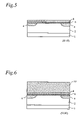
- FIG. 1 is a schematic cross-sectional view of a transistor according to the first embodiment.
- FIG. 2 is a flowchart illustrating a method for manufacturing a transistor according to the first embodiment.
- FIGS. 3 to 8 are schematic cross-sectional views illustrating each step of a method for manufacturing a transistor according to the first embodiment.
- FIG. 9 is a graph showing the carbon contents in a transistor according to the first embodiment.
- FIG. 10A shows concentration distributions of impurities in the conventional transistor.
- FIG. 10B shows concentration distributions of impurities in a transistor according to the first embodiment.
- FIG. 11 is a flowchart illustrating a method for manufacturing a transistor according to the second embodiment.
- FIG. 12 is a flowchart illustrating a method for manufacturing a transistor according to the third embodiment.
- a method for manufacturing a semiconductor device comprises the steps of: forming a first insulating film on a semiconductor substrate; forming a second insulating film on the first insulating film, the second insulating film having a relative permittivity higher than that of the first insulating film; and forming a gate electrode on the second insulating film.
- the second insulating film forming step includes: a first step of supplying a source gas (or a raw material gas) to a film forming apparatus so as to cause a raw material to be adsorbed to a surface of the first insulating film; a second step of purging excessive first source gas from the film forming apparatus by an inert gas; a third step of supplying an oxidizing gas to the film forming apparatus to oxidize the raw material adsorbed to the surface of the first insulating film; a fourth step of purging excessive first source gas from the film forming apparatus by an inert gas; a fifth step of generating reducing gas plasma within the film forming apparatus to produce active species, and causing the produced active species to react with an unoxidized portion of the raw material adsorbed to the surface of the first insulating film; and a sixth step of purging excessive first source gas from the film forming apparatus by an inert gas; wherein the first to sixth steps are repeated.
- FIG. 1 is a schematic cross-sectional view of a transistor according to the first embodiment of the present invention.
- impurities are implanted in a Si substrate 1 , forming a diffusion layer 2 , as shown in FIG. 1 .
- a first gate insulating film 6 is an interfacial gate insulating film of SiON.
- the second gate insulating film 8 is a thin film made up of a high dielectric constant film (High-k film) of HfO 2 , etc.
- the gate electrode 10 is formed of poly-silicon.
- a sidewall 12 is formed on the sides of the gate electrode 10 .
- the sidewall 12 is made of Si 3 N 4 .
- SD extensions 14 which are layers having a relatively low impurity concentration, are formed in the surface portion of the Si substrate 1 such that they extend outside of the gate electrode 10 . Furthermore, a source/drain 16 , which is a diffusion layer having a relatively large junction depth and a high impurity concentration, is also formed in the surface portion of the Si substrate 1 such that it extends outside of the SD extensions (outside of the sidewall 12 ).
- an isolation dielectric film 20 is deposited on the Si substrate 1 such that the gate electrode 10 , the sidewall 12 , etc. are buried in the isolation dielectric film 20 . Furthermore, contact plugs 22 are formed in the isolation dielectric film 20 such that they penetrate through the isolation dielectric film 20 to the source/drain 16 . Further, a wiring layer 24 is formed on the contact plugs 22 .
- the transistor of the first embodiment is configured as described above. It has the same structure as that of conventional transistors.
- the second gate insulating film 8 which is a High-k film, has a lower impurity content than conventional High-k films.
- the amount of C contained in the second gate insulating film 8 is smaller than the amount of N.
- FIG. 2 is a flowchart illustrating a method for manufacturing a transistor according to the first embodiment of the present invention.
- FIGS. 3 to 8 are schematic cross-sectional views illustrating each step of the method for manufacturing the transistor.
- impurities are implanted in the Si substrate 1 , forming the diffusion layer 2 , and then the device separation regions 4 are formed in the Si substrate 1 to separate each region of the Si substrate 1 .
- the surface of the Si substrate 1 is cleaned through HF cleaning in step S 102 .
- an SiON film used as a material for the first gate insulating film 6 is formed on the Si substrate 1 in step S 104 , as shown in FIG. 3 .
- the first gate insulating film 6 is formed of N 2 and N 2 O.
- an HfO 2 film used as a material for the second gate insulating film 8 is formed.
- the HfO 2 film (the second gate insulating film) is formed by repeating a cycle consisting of the supply and purge of a film-forming raw material for the second gate insulating film (steps S 106 and S 108 ), the supply and purge of an oxidizer (steps S 110 and S 112 ), and the supply and purge of active species (steps S 114 and S 116 ).
- step S 106 as a film-forming raw material 30 for the second insulating film, TEMAHf (tetrakis(ethylmethylamino)hafnium; Hf(NEtMe) 4 ) is supplied to a film forming apparatus (not shown) in which the substrate having the first gate insulating film 6 formed thereon has been placed. This causes a monomolecular layer of the film-forming raw material 30 to be chemically absorbed to the surface of the first insulating film 6 , as shown in FIG. 4 . Then, TEMAHf is purged from the film forming apparatus in step S 108 . After that, H 2 O is supplied to the film forming apparatus as an oxidizer in step S 110 without interruption.
- TEMAHf tetrakis(ethylmethylamino)hafnium
- NH 3 /Ar plasma is generated within the film forming apparatus to produce active species in step S 114 .
- the active species are purged from the film forming apparatus in step S 116 .
- the above six steps constitute one formation cycle, and this cycle is repeated a plurality of times.
- the HfO 2 film 8 is formed at a film formation rate of approximately 0.8 ⁇ /cycle. Therefore, when an HfO 2 film having a certain film thickness needs to be formed, the cycle may be repeated the number of times calculated from the film thickness. Thus, the HfO 2 film (the second gate insulating film) 8 having any desired film thickness can be formed.
- a poly-silicon film 6 used as a material for the gate electrode 10 is deposited on the second gate insulating film (HfO 2 film) 8 in step 120 , as shown in FIG. 6 .
- the poly-silicon film (gate electrode) 10 is formed by a CVD (Chemical Vapor Deposition) technique.
- the poly-silicon film (gate electrode) 10 is processed through lithographic and etching processes such that it has a predetermined gate length, as shown in FIG. 7 .
- the second gate insulating film (HfO 2 film) 8 and the first gate insulating film (SiON film) 6 are also etched such that they have the same width as the gate electrode 10 .
- ion implantation is carried out using the gate electrode 10 as a mask to form the SD extensions 14 , which are diffusion layers having a relatively small junction depth.
- step S 126 the sidewall 12 is formed on the sides of the gate electrode 10 , as shown in FIG. 8 . Specifically, first an SiN film, etc. is deposited such that the gate electrode 10 is buried in it. Then, the SiN film is etched back so as to leave the SiN film only on the sides of the gate electrode 10 , thus forming the sidewall 12 .
- step S 128 ion implantation is carried out using the gate electrode 10 and the sidewall 12 as a mask to form the source/drain 16 in the surface of the Si substrate 1 .
- the source/drain 16 is a diffusion layer having a high impurity concentration.
- activation annealing is performed in step S 130 to activate the impurities implanted in the SD extensions 14 and the source/drain 16 .
- an isolation dielectric film 20 is formed on the Si substrate 1 such that the gate electrode 10 , the sidewall 12 , etc. are buried under the isolation dielectric film 20 . Furthermore, the contact plugs 22 are formed in the isolation dielectric film 20 such that they penetrate through the isolation dielectric film 20 to the source/drain 16 . After that, the wiring layer 24 is formed on the contact plugs 22 .
- FIG. 9 is a graph showing the C (carbon) contents of HfO 2 films formed by a conventional ALD technique, the above-described “long purge” method, and the above method of the first embodiment, respectively.
- the horizontal axis represents the depth from the surface of each HfO 2 film and the vertical axis represents the C concentration (atoms/cm 3 ).
- Curve (a) indicates the C concentration (content) of the HfO 2 film formed by the conventional ALD technique;
- curve (b) indicates the C concentration of the HfO 2 film formed by the “long purge” method;
- curve (c) indicates the C concentration of the HfO 2 film formed by the method of the present embodiment which includes the step of supplying NH 3 /Ar plasma.
- the method of the first embodiment has reduced the C (carbon) content concentration of the HfO 2 film at every depth, as compared to the conventional ALD technique and the “long purge” method.
- the C concentration around the HfO 2 /Si interface has been dramatically reduced to approximately 1 ⁇ 10 19 atoms/cm 3 , as can be seen in the figure.
- This is considered to be attributed to the fact that in the case of the manufacturing method of the first embodiment including the step of supplying reducing gas plasma, excited radicals (NH, NH 2 , etc.) formed by the decomposition of NH 3 react with Hf—N—CH 3 C 2 H 5 adhered to the surface of the substrate and as a result, C and H are discharged as gas.
- the N content of the HfO 2 film increases as its C content decreases.
- FIGS. 10A and 10B show concentration distributions of each impurity. Specifically, FIG. 10A shows concentration distributions obtained when a conventional method is used, while FIG. 10B shows those obtained when the method of the present invention (the first embodiment) is used. As shown in the figures, the method of the present invention (the first embodiment) can reduce the concentrations of H (hydrogen) and N (nitrogen) as well as C. Especially, the impurity concentrations around the HfO 2 /SiO 2 and the SiO 2 /Si interfaces have been considerably reduced.
- the process of forming an HfO 2 film (High-k film) constituting the second gate insulating film 8 includes steps such as the supply and purge of active species (steps S 114 and S 116 ) in addition to the supply and purge of a film-forming raw material (S 106 and S 108 ) and the supply and purge of an oxidizer (S 110 and S 112 ).
- the above six steps constitute one cycle, and this cycle is repeated to form the second gate insulating film (HfO 2 film) 8 .
- This can reduce the concentrations of impurities such as C contained in the HfO 2 film, thereby reducing the leakage current and suppressing the formation of interfacial levels due to the impurities.
- the first embodiment can effectively prevent an increase in the impurity concentration around the interface, more effectively suppressing the formation of the interfacial levels and preventing a reduction in the mobility. Further according to the method of the first embodiment, the amount of N contained in the HfO 2 film increases, which prevents diffusion of Si around the interfaces with the substrate and the poly-Si electrode as well as preventing dopants (e.g., boron, etc.) contained in the poly-Si electrode from diffusing into the High-k film. Therefore, it is possible to produce a semiconductor device having good device characteristics.
- dopants e.g., boron, etc.
- a second embodiment of the present invention is characterized in that the second embodiment repeats the first to sixth steps of the first embodiment n times and then further repeats the first to fourth steps until the second insulating film is formed to a predetermined film thickness, where n is an integer equal to or less than 10.
- FIG. 11 is a flowchart illustrating a method for forming the second gate insulating film 6 according to the second embodiment of the present invention.
- the transistor of the second embodiment has the same structure as the transistor of the first embodiment.
- the process of the first embodiment for forming the second insulating film (HfO 2 film) 8 includes 6 steps, namely the supply and purge of a film-forming raw material (steps S 106 and S 108 ), the supply and purge of an oxidizer (steps S 110 and S 112 ), and the supply and purge of active species (steps S 114 and S 116 ).
- the above 6 steps constitute one cycle, and this cycle is simply repeated to form the second insulating film 8 .
- the method of the second embodiment first repeats the above 6-step cycle 10 times and then repeats the steps of the conventional ALD method, that is, the supply and purge of the film-forming raw material (steps 202 and S 204 ) and the supply and purge of the oxidizer (steps S 206 and S 208 ).
- the second insulating film 8 is formed in two stages.
- TEMAHf is supplied to the film forming apparatus as a film-forming raw material in step S 202 .
- This causes the film-forming raw material 30 to be absorbed to the Si substrate 1 .
- the film forming apparatus is purged in step S 204 .
- H 2 O is supplied as an oxidizer in step S 206 and then it is purged in step S 208 .
- ammonia radicals are supplied as reducing gas plasma instep S 210 and then they are purged in step S 212 .
- This 6-step cycle is repeated 10 times.
- the first four steps (S 202 , S 204 , S 206 , and S 208 ) are further repeated. That is, after the 10 th cycle, each cycle only consists of the first four steps, i.e., the supply and purge of TEMAHf and the supply and purge of H 2 O; the supply and purge of the active species (steps S 210 and S 212 ) are not performed.
- An HfO 2 film is formed at a film formation rate of approximately 0.8 ⁇ /cycle. Therefore, when an HfO 2 film having a certain film thickness needs to be formed, the cycle may be repeated the number of times calculated from the target film thickness.
- the gate electrode 10 After the HfO 2 film (the second insulating film) 8 having a desired film thickness is formed, the gate electrode 10 , the SD extensions 14 , the sidewall 12 , the source/drain 16 , etc. are formed (steps S 122 to S 132 ), as in the first embodiment, forming a semiconductor device similar to that of the first embodiment.
- the first 10 cycles each consists of 6 steps, i.e., the supply and purge of TEMAHf, the supply and purge of H 2 O, and the supply and purge of active species.
- each cycle includes only 4 steps, i.e., the supply and purge of TEMAHf and the supply and purge of H 2 O, which is identical to the conventional ALD method.
- the second gate insulating film is formed in two stages, and the steps of supplying the active species and purging them are omitted from the second stage.
- An HfO 2 film with a film thickness of 15 nm formed by the above method contains an amount of C approximately equal to that contained in an HfO 2 formed by the conventional ALD method.
- the method of the second embodiment can prevent an increase in the amount of C around the HfO 2 /Si interface, thereby reducing the amount of impurities around the interface, as compared to the conventional ALD technique. Reducing the amount of impurities around the interface can prevent an increase in the leakage current and a reduction in the mobility due to formation of an interfacial level, thereby enhancing the performance of the transistor.
- the first 10 cycles each include 6 steps, but the eleventh and later cycles each include only 4 steps identical to the steps of the conventional ALD technique. This arrangement allows producing semiconductor devices having good device characteristics without reducing the throughput.
- the method of the second embodiment first repeats the 6-step cycle (consisting of the supply and purge of a film-forming raw material, the supply and purge of an oxidizer, and the supply and purge of active species) 10 times and then repeats the 4-step cycle (not including the supply and purge of active species) a certain number of times.
- the present invention is not limited to this particular arrangement.
- the numbers of times the 6-step cycle (which includes the supply and purge of active species) and the 4-step cycle (which does not include the supply and purge of active species) are repeated may be determined considering the film thickness of the film to be formed, the maximum permissible impurity concentrations, etc.
- the steps of supplying active species and purging them are repeated a plurality of times (10 times) in the initial stage, effectively reducing the amount of impurities around the High-k/Si interface.
- the present invention is not limited to this particular arrangement in which only the first several cycles consist of 6 steps.
- some of the later cycles (4-step cycles) may include the supply and purge of active species.
- a film formation cycle consists of supplying a film-forming raw material in step S 202 , purging it in step S 204 , supplying an oxidizer in step S 206 , purging it in step S 208 , supplying active species in step S 210 , and purging them in step S 212 .
- the present invention is not limited to this particular cycle.
- four steps such as the supply and purge of an oxidizer (steps S 206 and S 208 ) and the supply and purge of active species (steps S 210 and S 212 ) may be repeated a plurality of times after performing the supply and purge of a film-forming raw material (steps S 202 and S 204 ).
- the above four steps are preferably repeated 1 to 10 times.
- the supply and purge of active species may be repeated a plurality of times within one cycle consisting of the supply and purge of a film-forming raw material (steps 202 and 204 ), the supply and purge of an oxidizer (steps 206 and 208 ), and the supply and purge of the active species (steps 210 and 212 ).
- the supply and purge of the active species are preferably repeated approximately 10 times. This arrangement can more effectively prevent impurities from accumulating around the interfaces.
- a method for manufacturing a semiconductor device comprises the steps of: forming a first insulating film on a semiconductor substrate; forming a second insulating film on the first insulating film, the insulating film being made up of a mixed film consisting of two or more types of insulating films, one of the two or more types of insulating films having a relative permittivity higher than that of the first insulating film; and forming a gate electrode on the second insulating film.
- the second insulating film forming step includes: a first step of supplying a first source gas (or a first raw material gas) to a film forming apparatus so as to cause a first raw material to be absorbed to a surface of the first insulating film; a second step of purging excessive first source gas from the film forming apparatus by an inert gas; a third step of supply a first oxidizing gas to the film forming apparatus to oxidize the first raw material absorbed to the surface of the first insulating film; a fourth step of purging excessive first source gas from the film forming apparatus by an inert gas; a fifth step of generating first reducing gas plasma within the film forming apparatus to produce first active species, and causing the produced first active species to react with an unoxidized portion of the first raw material absorbed to the surface of the first insulating film; a sixth step of purging excessive first source gas from the film forming apparatus by an inert gas; a seventh step of supplying a second source gas (or
- the first to twelfth steps may be sequentially repeated a plurality of times.
- the first to sixth steps may be sequentially repeated a plurality of times and then the seventh to twelfth steps may be sequentially repeated a plurality of times.
- FIG. 12 is a flowchart illustrating the method for forming a transistor according to the third embodiment of the present invention.
- the transistor of the third embodiment is almost the same as that of the first embodiment.
- the second gate insulating film 8 of the first embodiment is an HfO 2 film
- that of the third embodiment is made up of a mixed film consisting of an HfO 2 film and an Al 2 O 3 film.
- the method of the third embodiment for manufacturing the transistor is also almost the same as that of the first embodiment. However, as described in detail below, the method of the third embodiment is different from that of the first embodiment in the process of forming the second gate insulating film 8 , since they manufacture transistors having different second gate insulating films.
- the third embodiment performs a first series of 6 steps, namely the supply and purge of a first film-forming raw material (steps S 302 and S 304 ), the supply and purge of an oxidizer (steps S 306 and S 308 ), and the supply and purge of active species (steps S 310 and S 312 ), to form an HfO 2 film on the first gate insulating film formed on the substrate.
- HfCl 4 is supplied to the film forming apparatus as the first film-forming raw material in step S 302 , causing HfCl 4 to be absorbed to the surface of the first gate insulating film. Then, the film forming apparatus is purged in step 304 . After that, H 2 O is supplied as the oxidizer in step S 306 . Then, the film forming apparatus is purged in step S 308 . After that, hydrogen radicals are supplied as the reducer in step S 310 , and then the film forming apparatus is purged in step S 312 .
- the third embodiment performs a second series of 6 steps, namely the supply and purge of a second film-forming raw material (steps S 314 and S 316 ), the supply and purge of an oxidizer (steps S 318 and S 320 ), and the supply and purge of active species (steps S 322 and S 324 ), to form an Al 2 O 3 film.
- TMA trimethylaluminum; Al(CH 3 ) 3
- the film forming apparatus is purged in step S 316 .
- step S 318 O 2 radicals are supplied as the oxidizer in step S 318 .
- step S 320 the film forming apparatus is purged in step S 320 .
- step S 324 hydrogen radicals are supplied in step S 322 , and then the film forming apparatus is purged in step S 324 .
- Steps S 302 to S 312 for forming HfO 2 and steps S 314 to S 324 for forming Al 2 O 3 collectively constitute one formation cycle. This cycle is repeated a plurality of times to form an HfAlO x film as the second insulating film 8 , which is a mixed film consisting of an HfO 2 film and an Al 2 O 3 film.
- the gate electrode 10 , the SD extensions 14 , the sidewall 12 , the source/drain 16 , etc. are formed in the same manner as in the first embodiment, forming the transistor of the third embodiment.
- the third embodiment forms HfAlO, (film) as the second gate insulating film 8 , which is a mixed film consisting of High-k films.
- the supply and purge of active species are carried out in addition to the conventional 4 steps, i.e., the supply and purge of a film-forming raw material and the supply and purge of an oxidizer.
- a High-k film having a low impurity content can be formed, which makes it possible to produce a highly reliable transistor and a semiconductor device having good device characteristics.
- the third embodiment performs the supply and purge of a first film-forming raw material (steps S 302 and S 304 ), the supply and purge of an oxidizer (steps S 306 and S 308 ), and the supply and purge of active species (steps S 310 and S 312 ) to form HfO 2 and then performs the supply and purge of a second film-forming raw material (steps S 314 and S 316 ), the supply and purge of an oxidizer (steps S 318 and S 320 ), and the supply and purge of active species (steps S 322 and S 324 ) to form Al 2 O 3 .
- the supply and purge of active species may be omitted from either the first half cycle, from the supply of the first film-forming raw material to the purge of the active species (6 steps), or the second half cycle, from the supply of the second film-forming raw material to the purge of the active species (6 steps).
- the supply and purge of the active species (in steps S 310 and S 312 or steps S 322 and S 324 ) after supplying the first or second film-forming raw material may be repeated a plurality of times within one cycle, as in the second embodiment.
- the supply and purge of the oxidizer and the supply and purge of the active species may be repeated a plurality of times within one cycle, as in the second embodiment, which makes it possible to effectively prevent impurities from accumulating around the interfaces.
- the present embodiment performs the supply and purge of a first film-forming raw material (steps S 302 and S 304 ), the supply and purge of an oxidizer (steps S 306 and S 308 ), and the supply and purge of active species (steps S 310 and S 312 ) once and then performs the supply and purge of a second film-forming raw material (steps S 314 and S 316 ), the supply and purge of an oxidizer (steps S 318 and S 320 ), and the supply and purge of active species (steps S 322 and 5324 ).
- the present invention is not limited to this particular arrangement.
- the first half cycle (consisting of the supply and purge of the first film-forming raw material, the supply and purge of the oxidizer, and the supply and purge of the active species in steps S 302 to S 312 , respectively) may be repeated a plurality of times, and then the second half cycle (consisting of the supply and purge of the second film-forming raw material, the supply and purge of the oxidizer, and the supply and purge of the active species in steps S 314 to S 324 , respectively) may also be repeated a plurality of times.
- the number of times each half cycle is repeated may be adjusted to form a mixed film, or a multilayer film, made up of two or more types of insulating films (or layers) having desired film thicknesses, as the second gate insulating film.
- the first to third embodiments were described as applied when a single transistor is formed on the Si substrate 1 and therefore the accompanying drawings only show a single transistor on the Si substrate 1 .
- the present invention is not limited to semiconductor devices including only one transistor. They may include a plurality of transistors, such as CMOSFETs (complementary metal-oxide-semiconductor field effect transistors).
- the film forming methods of the first to third embodiments can be applied not only when a High-k film is formed as a gate insulating film, but also when other thin films are formed. That is, the present invention is particularly effective in forming High-k films having a low impurity content, metal wiring, etc. for capacitances, wiring, etc. as well as forming gate insulating films.
- the first to third embodiments form an SiON film as the first gate insulating film 6 .
- the first gate insulating film 6 of the present invention is not limited to SiON films.
- the first gate insulating film 6 may be an insulating film having a comparatively low relative permittivity, such as an SiN film or a thermal oxidation film.
- the first and second embodiments form an HfO 2 film, which is a High-k film having a higher relative permittivity than the first gate insulating film.
- the second insulating film is not limited to this particular type of High-k film. Another type of High-k film may be used.
- the second insulating film may be a High-k film made of Sc 2 O 3 , Y 2 O 3 , La 2 O 3 , Pr 2 O 3 , Nd 2 O 3 , Nb 2 O 3 , Sm 2 O 3 , EuO, Gd 2 O 3 , Tb 2 O 3 , Dy 2 O 3 , Ho 2 O 3 , Er 2 O 3 , Tm 2 O 3 , Lu 2 O 3 , ZrO 2 , TiO 2 , MoO 2 , WO 2 , MgO, ZnO, SnO, InO, Ta 2 O 3 , Al 2 O 3 , etc.
- the third embodiment forms an HfAlO x , film which is a mixed film of HfO 2 and Al 2 O 3 .
- the second insulating film of the present invention is not limited to this particular type of mixed film.
- the second insulating film may be a mixed film made up of some of the above High-k films.
- the second gate insulating film may be a mixed film made up of a High-k film and another type of film, for example, an HfSiO x film made up of an HfO 2 film and an SiO 2 film.
- the first to third embodiments use TEMAHf or HfCl 4 as a film-forming raw material to form an HfO 2 film.
- the HfO 2 film-forming raw material of the present invention is not limited to these materials.
- the film-forming raw material include Hf(OC(CH 3 ) 2 CH 2 OCH 3 ) 4 , Hf(OC(CH 3 ) 3 ) 4 , Hf[N(CH 3 ) 2 ] 4 , Hf[N(C 2 H 5 ) 2 ] 4 , Hf(NO 3 ) 4 , and Hf (C 11 H 19 O 2 ) 4 .
- the third embodiment uses TMA to form an Al 2 O 3 film.
- the Al 2 O 3 film-forming raw material of the present invention is not limited to this material.
- suitable examples of film-forming raw materials for an SiO 2 film constituting the second gate insulating film include, but are not limited to, Si(NEtMe) 4 , Si(OC(CH 3 ) 3 ) 4 , Si(OC 2 H 5 ) 4 , and (C 2 H 5 ) 2 SiH 2 .
- the first to third embodiments use H 2 O as an oxidizer.
- the oxidizer of the present invention is not limited to H 2 O.
- O 3 , O 2 , or O 2 radicals may be used.
- the first to third embodiments use ammonia radicals or hydrogen radicals as reducing gas plasma.
- the reducer of the present invention is not limited to these radicals.
- the reducer may be determined considering the film-forming raw material to be used, etc. For example, it may be N 2 or a mixed gas radical including NH 3 , H 2 , or N 2 .
- Si substrate 1 of the first to third embodiments in which the device separation regions 4 are formed corresponds to the base substrate (or the semiconductor substrate) of the present invention (indicated in the appended claims).
- the mixed film of the third embodiment made up of an HfO 2 film and an Al 2 O 3 film corresponds to the mixed film of the present invention made up of two or more types of insulating films (indicated in the appended claims).
- Step S 104 of the first to third embodiments corresponds to the first insulating film forming step of the present invention
- steps S 120 and S 122 of the first to third embodiments together correspond to the gate electrode forming step of the present invention (indicated in the appended claims).
- steps of the first and second embodiments correspond to steps of the present invention (indicated in the appended claims) as follows.
- Steps S 106 and S 202 correspond to the film-forming raw material supplying step; steps S 108 and S 204 , the film-forming raw material purging step; steps S 110 and S 206 , the oxidizer supplying step; steps S 112 and S 208 , the oxidizer purging step; steps S 114 and S 210 , the active species supplying step; and steps S 116 and S 212 , the active species purging step.
- Step S 302 corresponds to the first film-forming raw material supplying step; step S 304 , the first film-forming raw material purging step; step S 306 , the first oxidizer supplying step; step S 308 , the first oxidizer purging step; step S 310 , the first reducing gas plasma supplying step; step 312 , the first reducing gas plasma purging step; step 314 , the second film-forming raw material supplying step; step S 316 , the second film-forming raw material purging step; step S 318 , the second oxidizer supplying step; step S 320 , the second oxidizer purging step; step S 322 , the second reducing gas plasma supplying step; and step S 324 , the second reducing gas plasma purging step.
- a semiconductor device comprises: a semiconductor substrate; a first insulating film formed on the semiconductor substrate; a second insulating film formed on the first insulating film, the second insulating film having a relative permittivity higher than that of the first insulating film; a gate electrode formed on the second insulating film; a third insulating film formed on sides of the gate electrode; and a source/drain diffusion layer formed in the semiconductor substrate; wherein the carbon concentration of the second insulating film is lower than the nitrogen concentration of the second insulating film.
- heat treatment usually at approximately 1,000° C.
- HfO 2 film HfO 2 crystallizes due to the above heat treatment.
- the second insulating film contains N (nitrogen) or C (carbon), its material hardly crystallizes even during heat treatment.
- the amount of C is preferably smaller than the amount of N.
- the second insulating film contains N and C, which prevents the material of the High-k film to crystallize due to heat treatment. Furthermore, the carbon (C) concentration of the second insulating film is lower than the nitrogen (N) concentration, preventing an increase in the leakage current. In this case, the N concentration is preferably set to a value small enough not to change the threshold voltage Vth.
- the present invention performs the supply and purge of active species in addition to the conventional cycle consisting of the supply and purge of a film-forming raw material and the supply and purge of an oxidizer, which makes it possible to reduce the impurity content of the second insulating film. Therefore, it is possible to prevent an increase in the leakage current and thereby produce a semiconductor device having good device characteristics.
Abstract
Description
Claims (18)
Applications Claiming Priority (4)
| Application Number | Priority Date | Filing Date | Title |
|---|---|---|---|
| JP2003-307149 | 2003-08-29 | ||
| JP2003307149 | 2003-08-29 | ||
| JP2004187217A JP4887604B2 (en) | 2003-08-29 | 2004-06-25 | Manufacturing method of semiconductor device |
| JP2004-187217 | 2004-06-25 |
Publications (2)
| Publication Number | Publication Date |
|---|---|
| US20050048728A1 US20050048728A1 (en) | 2005-03-03 |
| US6984565B2 true US6984565B2 (en) | 2006-01-10 |
Family
ID=34220778
Family Applications (1)
| Application Number | Title | Priority Date | Filing Date |
|---|---|---|---|
| US10/917,288 Active US6984565B2 (en) | 2003-08-29 | 2004-08-13 | Method of manufacturing a semiconductor device |
Country Status (4)
| Country | Link |
|---|---|
| US (1) | US6984565B2 (en) |
| JP (1) | JP4887604B2 (en) |
| KR (1) | KR20050021335A (en) |
| TW (1) | TW200515470A (en) |
Cited By (2)
| Publication number | Priority date | Publication date | Assignee | Title |
|---|---|---|---|---|
| US20060102968A1 (en) * | 2004-11-15 | 2006-05-18 | International Business Machines Corporation | Nitrogen-containing field effect transistor gate stack containing a threshold voltage control layer formed via deposition of a metal oxide |
| US20080242071A1 (en) * | 2007-03-30 | 2008-10-02 | Taiwan Semiconductor Manufacturing Company, Ltd. | Method for passivating gate dielectric films |
Families Citing this family (17)
| Publication number | Priority date | Publication date | Assignee | Title |
|---|---|---|---|---|
| JP2005322668A (en) * | 2004-05-06 | 2005-11-17 | Renesas Technology Corp | Film deposition equipment and film deposition method |
| JP4456533B2 (en) * | 2005-06-14 | 2010-04-28 | 東京エレクトロン株式会社 | Silicon oxide film forming method, silicon oxide film forming apparatus, and program |
| JP2007012684A (en) * | 2005-06-28 | 2007-01-18 | Mitsubishi Electric Corp | Semiconductor device and manufacturing method of gate oxide film |
| JP4981283B2 (en) * | 2005-09-06 | 2012-07-18 | キヤノン株式会社 | Thin film transistor using amorphous oxide layer |
| JP4836761B2 (en) * | 2006-11-29 | 2011-12-14 | 株式会社日立国際電気 | Manufacturing method of semiconductor device |
| JP5039396B2 (en) * | 2007-02-19 | 2012-10-03 | ローム株式会社 | Manufacturing method of semiconductor device |
| EP2040300B1 (en) * | 2007-09-20 | 2016-07-06 | Imec | MOSFET devices and method to fabricate them |
| JP5679622B2 (en) * | 2008-01-31 | 2015-03-04 | 株式会社東芝 | Insulating film and semiconductor device using the same |
| KR101552937B1 (en) | 2009-01-29 | 2015-09-15 | 삼성전자주식회사 | Method of removing water from semiconductor substrate and method of atomic layer deposition using the same |
| JP5342903B2 (en) * | 2009-03-25 | 2013-11-13 | 株式会社東芝 | Semiconductor device |
| JP2010267925A (en) * | 2009-05-18 | 2010-11-25 | Hitachi Kokusai Electric Inc | Method for manufacturing semiconductor device and substrate processing apparatus |
| US20120181584A1 (en) * | 2011-01-19 | 2012-07-19 | Ru Huang | Resistive Field Effect Transistor Having an Ultra-Steep Subthreshold Slope and Method for Fabricating the Same |
| US9064891B2 (en) * | 2013-07-16 | 2015-06-23 | Globalfoundries Inc. | Gate encapsulation achieved by single-step deposition |
| US10153155B2 (en) * | 2015-10-09 | 2018-12-11 | University Of Florida Research Foundation, Incorporated | Doped ferroelectric hafnium oxide film devices |
| US10629749B2 (en) | 2017-11-30 | 2020-04-21 | Taiwan Semiconductor Manufacturing Co., Ltd. | Method of treating interfacial layer on silicon germanium |
| CN109103087A (en) * | 2018-07-13 | 2018-12-28 | 上海华力集成电路制造有限公司 | The manufacturing method of hafnium oxide gate dielectric layer |
| CN115044887A (en) * | 2022-06-27 | 2022-09-13 | 湖北九峰山实验室 | Preparation method of indium tin oxide film |
Citations (6)
| Publication number | Priority date | Publication date | Assignee | Title |
|---|---|---|---|---|
| US5576226A (en) * | 1994-04-21 | 1996-11-19 | Lg Semicon Co., Ltd. | Method of fabricating memory device using a halogen implant |
| US5882993A (en) * | 1996-08-19 | 1999-03-16 | Advanced Micro Devices, Inc. | Integrated circuit with differing gate oxide thickness and process for making same |
| JP2001274260A (en) | 2000-03-24 | 2001-10-05 | Matsushita Electric Ind Co Ltd | Semiconductor device and manufacturing method therefor |
| US6475910B1 (en) | 1999-03-11 | 2002-11-05 | Genus, Inc. | Radical-assisted sequential CVD |
| US6479400B2 (en) | 2000-07-27 | 2002-11-12 | Nec Corporation | Manufacturing method of system-on-chip and manufacturing method of semiconductor device |
| JP2003309188A (en) | 2002-04-15 | 2003-10-31 | Nec Corp | Semiconductor device and its manufacturing method |
Family Cites Families (4)
| Publication number | Priority date | Publication date | Assignee | Title |
|---|---|---|---|---|
| US6297539B1 (en) * | 1999-07-19 | 2001-10-02 | Sharp Laboratories Of America, Inc. | Doped zirconia, or zirconia-like, dielectric film transistor structure and deposition method for same |
| KR100502557B1 (en) * | 2000-09-18 | 2005-07-21 | 동경 엘렉트론 주식회사 | Method for film formation of gate insulator, apparatus for film formation of gate insulator, and cluster tool |
| US6844604B2 (en) * | 2001-02-02 | 2005-01-18 | Samsung Electronics Co., Ltd. | Dielectric layer for semiconductor device and method of manufacturing the same |
| JP4492783B2 (en) * | 2001-09-12 | 2010-06-30 | 日本電気株式会社 | Semiconductor device and manufacturing method thereof |
-
2004
- 2004-06-25 JP JP2004187217A patent/JP4887604B2/en active Active
- 2004-08-10 TW TW093123897A patent/TW200515470A/en unknown
- 2004-08-13 US US10/917,288 patent/US6984565B2/en active Active
- 2004-08-27 KR KR1020040067667A patent/KR20050021335A/en not_active Application Discontinuation
Patent Citations (6)
| Publication number | Priority date | Publication date | Assignee | Title |
|---|---|---|---|---|
| US5576226A (en) * | 1994-04-21 | 1996-11-19 | Lg Semicon Co., Ltd. | Method of fabricating memory device using a halogen implant |
| US5882993A (en) * | 1996-08-19 | 1999-03-16 | Advanced Micro Devices, Inc. | Integrated circuit with differing gate oxide thickness and process for making same |
| US6475910B1 (en) | 1999-03-11 | 2002-11-05 | Genus, Inc. | Radical-assisted sequential CVD |
| JP2001274260A (en) | 2000-03-24 | 2001-10-05 | Matsushita Electric Ind Co Ltd | Semiconductor device and manufacturing method therefor |
| US6479400B2 (en) | 2000-07-27 | 2002-11-12 | Nec Corporation | Manufacturing method of system-on-chip and manufacturing method of semiconductor device |
| JP2003309188A (en) | 2002-04-15 | 2003-10-31 | Nec Corp | Semiconductor device and its manufacturing method |
Non-Patent Citations (1)
| Title |
|---|
| Kawahara et al., "Effect of Purge Time on the Properties of HfO<SUB>2 </SUB>Films Prepared by Atomic Layer Deposition", IEICE Trans. Electron., vol. E87-C, No. 1, Jan. 2004. |
Cited By (5)
| Publication number | Priority date | Publication date | Assignee | Title |
|---|---|---|---|---|
| US20060102968A1 (en) * | 2004-11-15 | 2006-05-18 | International Business Machines Corporation | Nitrogen-containing field effect transistor gate stack containing a threshold voltage control layer formed via deposition of a metal oxide |
| US7242055B2 (en) * | 2004-11-15 | 2007-07-10 | International Business Machines Corporation | Nitrogen-containing field effect transistor gate stack containing a threshold voltage control layer formed via deposition of a metal oxide |
| WO2006055226A3 (en) * | 2004-11-15 | 2007-08-23 | Ibm | Nitrogen-containing field effect transistor gate stack containing a threshold voltage control layer formed via deposition of a metal oxide |
| US20080242071A1 (en) * | 2007-03-30 | 2008-10-02 | Taiwan Semiconductor Manufacturing Company, Ltd. | Method for passivating gate dielectric films |
| US7667247B2 (en) * | 2007-03-30 | 2010-02-23 | Taiwan Semiconductor Manufacturing Company, Ltd. | Method for passivating gate dielectric films |
Also Published As
| Publication number | Publication date |
|---|---|
| US20050048728A1 (en) | 2005-03-03 |
| TW200515470A (en) | 2005-05-01 |
| KR20050021335A (en) | 2005-03-07 |
| JP4887604B2 (en) | 2012-02-29 |
| JP2005101529A (en) | 2005-04-14 |
Similar Documents
| Publication | Publication Date | Title |
|---|---|---|
| US6984565B2 (en) | Method of manufacturing a semiconductor device | |
| US8102013B2 (en) | Lanthanide doped TiOx films | |
| US6806145B2 (en) | Low temperature method of forming a gate stack with a high k layer deposited over an interfacial oxide layer | |
| JP5103056B2 (en) | Manufacturing method of semiconductor device | |
| US7393736B2 (en) | Atomic layer deposition of Zrx Hfy Sn1-x-y O2 films as high k gate dielectrics | |
| KR101139194B1 (en) | Manufacturing method for semiconductor apparatus | |
| US7396719B2 (en) | Method of forming high dielectric film using atomic layer deposition and method of manufacturing capacitor having the high dielectric film | |
| US7510983B2 (en) | Iridium/zirconium oxide structure | |
| US8071452B2 (en) | Atomic layer deposition of hafnium lanthanum oxides | |
| US7989285B2 (en) | Method of forming a film containing dysprosium oxide and hafnium oxide using atomic layer deposition | |
| US20140327065A1 (en) | Conductive layers for hafnium silicon oxynitride films | |
| JP2003218108A (en) | CVD DEPOSITION OF M-SiO GATE DIELECTRIC | |
| US7601578B2 (en) | Defect control in gate dielectrics | |
| US7189660B2 (en) | Method of producing insulator thin film, insulator thin film, method of manufacturing semiconductor device, and semiconductor device | |
| US20050051857A1 (en) | Semiconductor device | |
| US7256145B2 (en) | Manufacture of semiconductor device having insulation film of high dielectric constant | |
| TW201518534A (en) | Method of cyclically depositing thin film, semiconductor manufacturing method, and semiconductor device | |
| EP1425785A2 (en) | Method of fabricating a gate stack at low temperature | |
| JP2006060155A (en) | Semiconductor device and its manufacturing method |
Legal Events
| Date | Code | Title | Description |
|---|---|---|---|
| AS | Assignment |
Owner name: SEMICONDUCTOR LEADING EDGE TECHNOLOGIES, INC., JAP Free format text: ASSIGNMENT OF ASSIGNORS INTEREST;ASSIGNOR:KAWAHARA, TAKAAKI;REEL/FRAME:015685/0384 Effective date: 20040728 |
|
| AS | Assignment |
Owner name: RENESAS TECHNOLOGY CORP., JAPAN Free format text: ASSIGNMENT OF ASSIGNORS INTEREST;ASSIGNOR:SEMICONDUCTOR LEADING EDGE TECHNOLOGIES, INC.;REEL/FRAME:016206/0616 Effective date: 20050601 |
|
| STCF | Information on status: patent grant |
Free format text: PATENTED CASE |
|
| FEPP | Fee payment procedure |
Free format text: PAYOR NUMBER ASSIGNED (ORIGINAL EVENT CODE: ASPN); ENTITY STATUS OF PATENT OWNER: LARGE ENTITY |
|
| FPAY | Fee payment |
Year of fee payment: 4 |
|
| AS | Assignment |
Owner name: RENESAS ELECTRONICS CORPORATION, JAPAN Free format text: CHANGE OF NAME;ASSIGNOR:RENESAS TECHNOLOGY CORP.;REEL/FRAME:024953/0224 Effective date: 20100401 |
|
| FEPP | Fee payment procedure |
Free format text: PAYOR NUMBER ASSIGNED (ORIGINAL EVENT CODE: ASPN); ENTITY STATUS OF PATENT OWNER: LARGE ENTITY Free format text: PAYER NUMBER DE-ASSIGNED (ORIGINAL EVENT CODE: RMPN); ENTITY STATUS OF PATENT OWNER: LARGE ENTITY |
|
| FPAY | Fee payment |
Year of fee payment: 8 |
|
| FPAY | Fee payment |
Year of fee payment: 12 |
|
| AS | Assignment |
Owner name: RENESAS ELECTRONICS CORPORATION, JAPAN Free format text: CHANGE OF ADDRESS;ASSIGNOR:RENESAS ELECTRONICS CORPORATION;REEL/FRAME:044928/0001 Effective date: 20150806 |