US7005350B2 - Method for fabricating programmable memory array structures incorporating series-connected transistor strings - Google Patents
Method for fabricating programmable memory array structures incorporating series-connected transistor strings Download PDFInfo
- Publication number
- US7005350B2 US7005350B2 US10/335,089 US33508902A US7005350B2 US 7005350 B2 US7005350 B2 US 7005350B2 US 33508902 A US33508902 A US 33508902A US 7005350 B2 US7005350 B2 US 7005350B2
- Authority
- US
- United States
- Prior art keywords
- stripes
- recited
- channel
- dielectric layer
- gate
- Prior art date
- Legal status (The legal status is an assumption and is not a legal conclusion. Google has not performed a legal analysis and makes no representation as to the accuracy of the status listed.)
- Expired - Lifetime, expires
Links
Images


Classifications
-
- H—ELECTRICITY
- H10—SEMICONDUCTOR DEVICES; ELECTRIC SOLID-STATE DEVICES NOT OTHERWISE PROVIDED FOR
- H10B—ELECTRONIC MEMORY DEVICES
- H10B43/00—EEPROM devices comprising charge-trapping gate insulators
- H10B43/30—EEPROM devices comprising charge-trapping gate insulators characterised by the memory core region
-
- H—ELECTRICITY
- H10—SEMICONDUCTOR DEVICES; ELECTRIC SOLID-STATE DEVICES NOT OTHERWISE PROVIDED FOR
- H10B—ELECTRONIC MEMORY DEVICES
- H10B69/00—Erasable-and-programmable ROM [EPROM] devices not provided for in groups H10B41/00 - H10B63/00, e.g. ultraviolet erasable-and-programmable ROM [UVEPROM] devices
-
- G—PHYSICS
- G11—INFORMATION STORAGE
- G11C—STATIC STORES
- G11C16/00—Erasable programmable read-only memories
- G11C16/02—Erasable programmable read-only memories electrically programmable
- G11C16/04—Erasable programmable read-only memories electrically programmable using variable threshold transistors, e.g. FAMOS
- G11C16/0483—Erasable programmable read-only memories electrically programmable using variable threshold transistors, e.g. FAMOS comprising cells having several storage transistors connected in series
-
- H—ELECTRICITY
- H10—SEMICONDUCTOR DEVICES; ELECTRIC SOLID-STATE DEVICES NOT OTHERWISE PROVIDED FOR
- H10B—ELECTRONIC MEMORY DEVICES
- H10B53/00—Ferroelectric RAM [FeRAM] devices comprising ferroelectric memory capacitors
Definitions
- the present invention relates to semiconductor integrated circuits containing memory arrays, and in preferred embodiments the invention particularly relates to monolithic three-dimensional memory arrays having series-connected memory cells.
- NAND flash and NROM flash EEPROM memory arrays are known to achieve relatively small memory cells.
- Other small flash EEPROM cells are known which use hot electron programming, such as NROM and floating gate NOR flash memory arrays. Such memory cells are less desirable for a 3D memory because they use many masks to produce a memory layer, and some use relatively high programming currents.
- Aritome entitled “Semiconductor Memory Device on which Selective Transistors are Connected to a Plurality of Respective Memory Cell Units,” describes a NAND flash memory array having TFT block select devices and bulk silicon flash cell devices.
- U.S. Pat. No. 5,621,683 by N. D. Young entitled “Semiconductor Memory with Non-Volatile Memory Transistor,” describes a memory array including TFT memory cells of a dielectric storage type arranged in a configuration other than a NAND architecture.
- An extremely dense memory array may be achieved by using thin film transistors having a charge storage dielectric, and which are connected in a NAND-style architecture.
- a flash memory array may be formed by series-connected NAND strings of SONOS memory cell devices.
- Each NAND string of memory cells includes a first block select device which couples one end of the NAND string to a global bit line, and a second block select device which couples the other end of the NAND string to a shared bias node associated with the string.
- the block select devices are also SONOS devices and may be formed in an identical fashion as the memory cell transistors, thus reducing the number of different structures necessary for each NAND string.
- Pairs of NAND strings within a memory block on a level of the memory array preferably share the same global bit line.
- Two block select signals for the block are routed to each NAND string.
- Each of the NAND strings within the block share the same word lines, but their control signals are reversed for the pairs of NAND strings.
- the first block select signal couples one NAND string to the global bit line and couples the other NAND string to a first shared bias node
- the second block select signal couples the other NAND string to the global bit line and couples the first NAND string to a second shared bias node.
- the block select devices and the memory cells devices are SONOS devices.
- a range of threshold voltages is contemplated, but preferably such devices are formed having a depletion mode threshold voltage.
- the block select devices and the memory cells devices are N-channel devices having a thermal equilibrium threshold voltage of ⁇ 2 to ⁇ 3 volts.
- a threshold voltage preferably corresponds to an erased data state, and the memory cells are programmed to a near depletion threshold voltage of from ⁇ 1 volt to 0 volts.
- the block select devices are preferably fabricated having the same thermal equilibrium threshold voltage but are maintained in a programmed state having a near depletion mode threshold voltage.
- a multi-level memory array includes memory cells formed on each of several memory planes or memory levels.
- NAND strings on more than one layer may be connected to global bit lines on a single layer.
- Such a global bit line layer is preferably disposed on a layer of a monolithic integrated circuit below all the memory levels for more convenient connection to support circuitry for the memory array, which may be disposed in the substrate below the array.
- a global bit line layer may reside in the midst of the memory levels, or above the array.
- the NAND strings on more than one layer may also be connected to shared bias nodes on a single layer, which preferably is disposed above all the memory levels.
- the shared bias nodes may reside in the midst of the memory levels, or below the array.
- the shared bias nodes may likewise be disposed on more than one layer.
- the present invention in preferred embodiments achieves a 4F 2 layout for each memory cell. Moreover, by interleaving the NAND strings on each memory level and using more than one shared bias node per block, very little additional overhead is required for the switch devices at each end of the NAND strings.
- the NAND strings on different levels are preferably connected together by way of vertical stacked vias. Each stacked via preferably connects to a channel or word line feature on more than one memory level.
- the invention is particularly well suited for a three-dimensional memory array because each level of memory cells may be produced with an average of less than three masks per level: one for defining channel stripes on each memory level, another for defining gate stripes on each memory level, and a via mask shared by at least three memory levels.
- An exemplary eight level memory array may be formed using only 19 masking steps.
- preferred embodiments of the present invention provide a memory array which may be programmed and erased using only tunneling currents, and which does not form leakage paths through non-selected memory cells in the memory array. Consequently, a memory of even greater density may be achieved since the memory array may be sized with relatively little regard for such unwanted leakage currents.
- the invention in several aspects is suitable for integrated circuits having a memory array, for memory cell and memory array structures, for methods for operating such integrated circuits and memory arrays, for methods for forming or fabricating such integrated circuits and memory arrays, and for computer readable media encodings of such integrated circuits or memory arrays, all as described herein in greater detail and as set forth in the appended claims.
- FIG. 1 is a perspective view of a multi-level array structure in accordance with an embodiment of the present invention, showing series-connected NAND strings.
- FIG. 2 is a cross-sectional view of a similar structure to that shown in FIG. 1 .
- FIG. 3 is a schematic diagram of a 4:1 interleaved NAND string structure in accordance with an embodiment of the present invention.
- FIG. 4 is a schematic diagram of a several NAND strings within a memory level, in accordance with an embodiment of the present invention.
- FIG. 5 is a schematic diagram as in FIG. 4 , showing exemplary read conditions for an embodiment of the present invention.
- FIG. 6 is a diagram depicting exemplary waveforms for the exemplary read conditions of FIG. 5 .
- FIG. 7 is a schematic diagram as in FIG. 4 , showing exemplary program conditions for an embodiment of the present invention.
- FIG. 8 is a diagram depicting exemplary waveforms for the exemplary program conditions of FIG. 7 .
- FIG. 9 is a schematic diagram as in FIG. 4 , showing exemplary erase conditions for an embodiment of the present invention.
- FIG. 10 is a diagram depicting exemplary waveforms for the exemplary erase conditions of FIG. 9 .
- FIG. 11 is a schematic diagram depicting the interconnection of NAND strings on each of several memory levels, in accordance with an embodiment of the present invention.
- FIG. 12 shown as FIGS. 12 A and FIG. 12B , is a flow diagram of an exemplary semiconductor process flow for forming a memory array in accordance with various embodiments of the present invention.
- FIG. 13 is a flow diagram of a portion of an exemplary semiconductor process flow for forming a charge storage dielectric for a memory array in accordance with various embodiments of the present invention.
- FIG. 14 is a flow diagram of a portion of an exemplary semiconductor process flow for forming a gate layer for a memory array in accordance with various embodiments of the present invention.
- FIG. 15 is a flow diagram of a portion of an exemplary semiconductor process flow for forming a gate layer for a memory array in accordance with various embodiments of the present invention.
- FIG. 16 is a flow diagram of a portion of an exemplary semiconductor process flow for forming a silicide layer for a memory array in accordance with various embodiments of the present invention.
- FIG. 17 is a perspective view of a partially-completed memory array level, in accordance with various embodiments of the present invention.
- FIG. 18 is a perspective view of a partially-completed memory array level, in accordance with various embodiments of the present invention.
- FIG. 19 is a cross-sectional view of a portion of a NAND string within a memory array level, in accordance with various embodiments of the present invention.
- FIG. 20 is a cross-sectional view of a portion of a NAND string within a memory array level, in accordance with various embodiments of the present invention.
- FIG. 21 is a cross-sectional view of a portion of a NAND string within a memory array level, and showing an upper-portion of an underlying memory array level, in accordance with various embodiments of the present invention.
- FIG. 22 is a cross-sectional view along a gate stripe and cutting across several NAND strings within a memory array level, and showing an upper-portion of an underlying memory array level, in accordance with various embodiments of the present invention.
- FIG. 23 is a cross-sectional view between gate stripes and cutting across a NAND string within a memory array level, in accordance with various embodiments of the present invention.
- FIG. 24 is a cross-sectional view of a via structure (i.e., a “zia”) making contact to three layers of the memory array, in accordance with various embodiments of the present invention.
- a via structure i.e., a “zia”
- FIG. 25 is a layout diagram of a zia and three memory array layers which corresponds to the zia structure shown in FIG. 24 .
- FIG. 26 is a layout diagram of a multi-level 4:1 interleaved NAND string memory array structure which corresponds to the schematic diagram shown in FIG. 3 , and includes zias as depicted in FIG. 24 .
- FIG. 27 is a cross-sectional view depicting the vertical interconnection of between the channel strings and gate strings within eight memory levels by use of only three zia levels, in accordance with various embodiments of the present invention.
- FIG. 28 is a cross-sectional view of a via structure (i.e., a “zia”) making contact to four channel string layers of a multi-level memory array, in accordance with various embodiments of the present invention.
- a via structure i.e., a “zia”
- FIG. 29 is a cross-sectional view of a chimney-like via structure (i.e., a “zia”) making contact to four channel string layers of a multi-level memory array, in accordance with various embodiments of the present invention.
- a chimney-like via structure i.e., a “zia”
- FIG. 30 is a layout diagram of a multi-level 2:1 interleaved NAND string memory array structure which might include zias as depicted in FIG. 29 .
- an integrated circuit having a three-dimensional memory array is assumed to be a monolithic integrated circuit, rather than an assembly of more than one monolithic integrated circuit.
- FIG. 1 a three-dimensional view is shown conceptually depicting a portion of a two-level memory array 100 in accordance with the present invention.
- a plurality of channel stripes e.g., 102
- a stored charge dielectric layer 104 such as an oxide/nitride/oxide (ONO) stack, is formed at least on the top surface of the channel stripes 102 .
- a plurality of gate stripes e.g., 106 ) running in a second direction different than the first direction is formed on the stored charge dielectric layer 104 .
- the gate stripes also called word line stripes, run generally orthogonally to the channel stripes.
- a source/drain region (e.g., 110 ) is formed in the channel stripes in the exposed regions between the word line stripes (i.e., not covered by a word line stripe), thus forming a series-connected string of thin-film transistors (TFT).
- TFT thin-film transistors
- Such channel stripes 102 are preferably formed by depositing a polycrystalline polysilicon layer and etching the layer using a channel mask to form the channel stripes.
- the word line stripes 106 may be formed of a stack of more than one layer, such as a polysilicon layer covered by a silicide layer, or may be a three level stack, as shown in the figure, all as described in greater detail herebelow.
- An interlevel dielectric layer 108 is formed above the word line stripes to isolate the word lines on one level (e.g., word line stripes 106 depicted on level 1) from the channel stripes on the next higher level (e.g., channel stripes 102 depicted on level 2). As is described in greater detail below, a dielectric may also be used to fill spaces between the word line stripes of a given level.
- FIG. 2 shows a cross-sectional view of such a plurality of series-connected transistors, which may also be referred to as a series-connected transistor string, and also as a series-connected NAND string.
- Four word lines 106 are shown, forming four individual transistors connected in series along the channel stripe 102 .
- the channel stripe 102 is formed from a lightly-doped p-type (i.e., P ⁇ doped) polycrystalline layer, and includes a heavily-doped n-type (i.e., N+ doped) source/drain region 110 formed in the channel stripe 102 between the word lines 106 .
- each respective transistor is formed in the channel stripe 102 beneath the respective word line 106 , and preferably includes a channel dopant region 112 to adjust the transistor threshold, lying above a P ⁇ region of the channel stripe 102 .
- a via 114 is depicted connected to one end of the channel stripe 102 for making connections to support circuitry for the array, as described in greater detail herebelow.
- the transistors of such a NAND string may be fabricated to contain enhancement or depletion mode devices for the programmed state.
- the erased state is often a zero-volt threshold voltage (VT) or even a depletion mode VT.
- VT zero-volt threshold voltage
- a floating gate device can have a wide range of V T s because the floating gate can store a wide range of charge levels. Consequently, it is more straightforward to make a depletion mode programmed state, as is described in “A Negative Vth Cell Architecture for Highly Scalable, Excellently Noise-Immune, and Highly Reliable NAND Flash Memories” by Takeuchi et al., in IEEE JSSC, Vol. 34, No. 5, May 1999, pp. 675-684. Achieving such a depletion mode erased state has not been done before in a NAND array incorporating SONOS devices.
- utilizing depletion mode devices when erased and near depletion mode devices i.e., around zero volt V T
- near depletion mode devices when programmed
- the cell current can pass more easily through the string even if unselected memory cells are programmed. This voltage reduction is beneficial for reducing disturb effects during the many expected read cycles. For example, an unselected memory cell on an unselected NAND string which is erased could be slowly disturbed to a programmed stated by higher voltages on the word lines.
- the memory structure of FIG. 2 may be fabricated using only two masking layers per memory level-one to define the channel stripes, and another to define the word line stripes. As is described herebelow, a third mask for contacting the layers of the memory level is not necessarily required, as contact structures may be incorporated that achieve electrical connection to at least three layers using a single via mask.
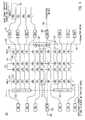
- FIG. 3 an electrical schematic is shown of a portion of an exemplary memory array.
- the portion shown may represent a two-dimensional array having only one plane of memory cells, or may represent one level of three-dimensional memory array having more than one level (i.e., more than one plane) of memory cells.
- a plurality of series-connected NAND transistor strings is shown, one of which is labeled 122 .
- Each string includes a plurality of SONOS transistors connected in series, each gated by a respective one of a plurality of word lines 125 .
- the NAND string 122 also includes a block select device 148 for coupling one end of the NAND string to a global bit line contact 131 in accordance with a block select signal BSEL 2 conveyed on node 126 , and further includes a second block select device 147 for coupling the other end of the NAND string to a shared bias node 128 in accordance with a block select signal BSEL 1 conveyed on node 124 .
- the global bit line contact 131 is shared with another NAND string 132 which is disposed on the other side of (i.e., opposite) the global bit line contact 131 and is independently selectable by another block select signal BSEL 3 .
- a group of four laterally adjacent NAND strings share a common bias node 128 , which may be termed VDRAIN 1 , disposed at the left end of the NAND strings, but are individually coupled to a respective one of four global bit line contacts disposed at the right end of the NAND string.
- VDRAIN 1 a common bias node disposed at the left end of the NAND strings
- VDRAIN 2 a common bias node disposed at the right end of the NAND strings.
- block select signal BSEL 1 couples the left end of half of the NAND strings to an associated global bit line, while the same signal couples the right end of the other half of the NAND strings to the shared bias node VDRAIN 1 .
- block select signal BSEL 2 couples the right end of half of the NAND strings to an associated global bit line, while the same signal couples the right end of the other half of the NAND strings to the shared bias node VDRAIN 2 .
- This structure interleaves the NAND strings by coupling two different NAND strings to the same global bit line.
- the left end of NAND string 134 is coupled by BSEL 1 to a global bit line contact 138
- the right end of NAND string 136 is coupled by BSEL 2 to a global bit line contact 140 .
- These two global bit line contacts 138 and 140 are preferably connected to the same global bit line, which may be routed horizontally on a wire 146 conveyed on a different wiring level.
- Such global bit lines may be conveyed a wiring level below the array, or alternatively above the array, or alternatively on a wiring level within the array (e.g., in a three-dimensional array having more than one level).
- the NAND string 134 and 136 may be referred to as “adjacent” NAND strings, as sharing the same global bit line and sharing the same word lines (i.e., within the same block of the array), even though there is another NAND string disposed between them. It is still possible to select only one of these two NAND strings for reading and writing because the shared bias nodes VDRAIN 1 and VDRAIN 2 are distinct and may be driven to different conditions, as is described in regards to the next several figures.
- Each of these two shared bias nodes VDRAIN 1 and VDRAIN 2 is shared by NAND strings in two adjacent blocks, and thus are preferably conveyed in vertical wires 142 and 144 , respectively, which are preferably conveyed on a wiring level “above” the memory array (i.e., further from the semiconductor substrate). Consequently, the two shared bias nodes VDRAIN 1 and VDRAIN 2 , the block select signals BSEL 1 and BSEL 2 , and the various word lines 125 , which all traverse across the memory array in the same direction, may be more conveniently decoded and driven to appropriate levels.
- the memory cells in the NAND strings are preferably SONOS structures.
- SONOS is meant to refer to the general class of transistor devices having a charge storage dielectric layer between the gate and the underlying channel, and is not used in a restrictive sense to merely imply a literal silicon-oxide-nitride-oxide-silicon layer stack.
- dielectric layers may be employed, such as oxynitrides, as is described in greater detail herebelow.
- a basic NAND string is a very efficient structure, capable of achieving a 4F 2 layout for the incremental transistor memory cell.
- providing the necessary switch devices with appropriate control signals at the ends of the NAND strings, and the overhead of connecting such NAND strings to global bit lines and to bias or ground nodes frequently degrades the resultant total efficiency.
- the structure depicted in FIG. 3 achieves very dense layout because of the interleaving of two NAND strings, both coupled to the same global bit line, thus relaxing the pitch requirements for the global bit lines by a factor of two.
- the structure depicted in FIG. 3 also achieves very dense layout because only one control signal is utilized at each end of the NAND strings.
- the block select devices may be SONOS devices just like the memory cell devices.
- each memory level consequently includes only one type of device, further simplifying the fabrication of each level.
- the block select devices may be sized identically to the memory cell devices, but preferably may have a longer channel length (i.e., wider polysilicon stripe for the block select signals) to increase the breakdown voltage of the block select devices.
- the memory cell devices and block select devices are both SONOS devices which are implanted to shift the thermal equilibrium (i.e., minimum trapped charge in the nitride) threshold voltage V T to depletion mode.
- a depletion mode implant that is a slow diffuser, preferably antimony or arsenic, is preferably used because of the relatively higher diffusion of such dopants in a polycrystalline layer compared with a crystalline substrate, and also due to the extremely small dimensions of the devices.
- the erased state V T is substantially depletion mode, preferably ⁇ 2 V to ⁇ 3 V threshold, while the programmed state V T is preferable about zero volts.
- the memory cells are programmed or erased to one of the two threshold voltages according to the data state, but the block select devices are preferably programmed to have about a zero-volt threshold voltage and maintained in this programmed state
- FIG. 4 a schematic diagram is introduced showing two different NAND strings in each of two blocks which may be coupled to the same global bit line.
- the terminology and structure described here is used in the next several figures to describe the basic read, program, and erase functions for such an array configuration.
- the portion shown may represent a two-dimensional array having only one plane of memory cells, or may represent one level of three-dimensional memory array having more than one level of memory cells.
- the basic operation will be described in the context of a single memory level and also for a multi-level array.
- the upper left NAND string is assumed to be the selected NAND string.
- the selected word line 168 is driven to a V WL voltage, and the selected memory cell 169 is indicated by an “S.”
- Other non-selected word lines 166 in the same block as the selected word line 168 may be termed “passing” word lines because these are usually driven to a V WLPASS voltage suitable to pass current through its respective memory cell 167 irrespective of the stored data state in its respective memory cell 167 . Only two such passing word lines 166 and one selected word line 168 are depicted, but it should be appreciated that in practice each NAND string may include many word lines, such as 16 total word lines.
- One end of the selected NAND string is coupled to a global bit line 162 by select device 165 which is controlled by a block select signal conveyed on node 164 having a voltage at any given time known as the V BSELB voltage, which signal may be thought of as the block select signal coupling the selected NAND string to the global bit line.
- the other end of the selected NAND string is coupled to a shared bias node 172 by select device 171 which is controlled by a block select signal conveyed on node 170 having a voltage of V BSELD , which signal may be thought of as the block select signal coupling the selected NAND string to the shared drain line.
- the voltage of the shared drain line 172 may be known as the V DRAIN voltage.
- Another NAND string (not shown) within the block just above the selected block is also coupled to the global bit line 162 by a select device 173 which is controlled by a block select signal conveyed on node 176 having a voltage at any given time known as the V UNBSEL voltage, which signal may be thought of as an unselected block select signal.
- the two select devices 173 and 165 preferably share a global bit line contact.
- An adjacent NAND string is also depicted just to the right of the selected NAND string.
- such adjacent NAND strings share the same word lines and are coupled to the same global bit line (i.e., by two different block selected signals), but do not share the same shared bias node (i.e., “drain” node).
- the adjacent NAND string includes devices 181 , 183 , 185 , and 187 .
- the lower end of this adjacent NAND string is coupled to the global bit line 162 by select device 187 which is controlled by the block select signal conveyed on node 170 , here referred to as V BSELD .
- the upper end of this adjacent NAND string is coupled to a shared bias node 174 by select device 181 which is controlled by the block select signal conveyed on node 164 , V BSELB .
- the voltage of the shared drain line 174 may be known as the V DADJ voltage, representing the drain voltage for an adjacent NAND string.
- the memory cell devices in the adjacent NAND string merit brief mention, for their respective bias conditions in the various operating modes are important.
- Two memory cell devices labeled 183 are driven by a passing word line 166 and may be termed unselected memory cells (labeled with a “U”).
- Another memory cell device 185 is driven by the selected word line 168 and may be termed a half selected memory cell (labeled with an “H”). Such unselected and half-selected memory cells are found in other non-selected NAND strings across the selected memory block.
- NAND strings are also depicted which are located in the block just below the selected array block. Both of these NAND strings are unselected.
- the block select line 176 at end of both NAND strings and the other block select line 180 at the other end of the NAND strings are both biased at an unselected block select voltage, V UNBSEL .
- An unselected word line 178 (representing the plurality of word lines in the unselected block) is biased at an unselected word line voltage, V WLUNSEL .
- An unselected shared drain node 182 is shown, having a bias voltage of V DUNSEL . Such a shared drain node is representative of any such drain node serving two unselected blocks.
- These two lower NAND strings also represent the bias voltages impressed on the various nodes and devices within other non-selected blocks on the same level as the selected block.
- these two lower NAND strings also represent the bias voltages impressed on the various nodes and devices within all blocks on the non-selected levels in the array.
- Block select devices 187 and 189 share a contact to global bit line 162 .
- a shared bias node (i.e., VDRAIN) contact is also shared by a respective block select device on opposite sides of the shared contact (e.g., select devices 171 and 175 ).
- select devices 171 and 175 select devices 171 and 175 .
- four NAND strings within the same block share such a VDRAIN contact (although each is coupled to a respective global bit line) for a total of eight NAND strings on a given layer sharing each VDRAIN contact.
- the selected NAND string is read by impressing a voltage across the NAND string, ensuring that both block select devices are biased to pass a current, ensuring that all non-selected memory cell devices in the NAND string are biased to pass a current through the string irrespective of the data state stored therein, and biasing the selected word line so that current flows through the NAND string for only one of the two data states.
- One suitable set of read conditions includes driving the “global bit line” block select line V BSELB to a positive power supply voltage V DD (e.g., V DD frequently being in the range from 2.5 to 3.3 volts) and driving the “drain” block select line V BSELD also to V DD .
- the voltage of the global bit line 162 (i.e., V GBL ) is approximately 2 volts, and V DRAIN is approximately 2.5 volts.
- the data state of the selected memory cell may be determined by maintaining the voltage bias on the global bit line and sensing current flow on the global bit line by a sensing circuit 190 , which may be either directly coupled to the global bit line or may be shared among several global bit lines and coupled by decoding circuitry to a desired global bit line.
- Suitable voltage-clamped bit line sensing circuits are described in “Current Sensing Method and Apparatus Particularly Useful for a Memory Array of Cells Having Diode-Like Characteristics” by Roy E. Scheuerlein, U.S. application Ser. No. 09/896,468, filed Jun. 29, 2001, which application is hereby incorporated by reference in its entirety.
- all the word lines in the selected block are driven to approximately 2 volts to charge the intermediate nodes of the selected NAND string (i.e., the source/drain regions between each device) to a voltage having a value between the V GBL voltage and the V DRAIN voltage. Then the selected word line is decreased to approximately 1 volt so that current will still flow through the selected device 169 if erased (i.e., having a threshold of around ⁇ 2 volts) and yet will prevent current flow if the selected device 166 is programmed (i.e., having a threshold of around 0 volts).
- the V DADJ voltage is preferably driven to substantially the same voltage as the V GBL voltage, so that substantially no bias voltage is impressed across the adjacent NAND string. Consequently, even though its block select devices 181 and 187 are turned on, no current flows through the adjacent NAND string onto the global bit line 162 which would interfere with sensing the current on the global bit line 162 .
- the intermediate nodes in the adjacent NAND string are all biased at approximately 2 volts since only the selected word line 168 is at a voltage lower than 2 volts, and since every memory cell and block select device has a threshold no higher than approximately 0 volts.
- the read disturb condition on the unselected devices 183 i.e., the bias voltage from gate to source/drain
- read disturb condition for the half selected cell 185 is approximately ⁇ 1 volt.
- the read disturb condition on the “F” devices 167 is approximately 0-0.5
- the read disturb bias on the selected device 169 is approximately ⁇ 1 volt.
- the read condition has very low gate-to-source bias voltages impressed across the selected memory cell device because the threshold voltage of an erased cell has been shifted to approximately ⁇ 2 volts.
- a ⁇ 1 volt gate-to-source voltage is sufficient to cause conduction through the transistor for the erased state but not for the programmed state, and thus allows discerning the data state of the cell.
- the depletion mode erased state allows all four memory cell devices (i.e., S, F, H, and U) to have very low read disturb bias, but is particularly important for the unselected “U” devices to have virtually no read disturb bias voltage, as a given memory cell must endure many more cycles biased as a “U” device than any other bias condition.
- the NAND strings in the unselected blocks are decoupled from the global bit lines by ensuring that the respective block select devices, such as devices 173 and 189 , remain off.
- the NAND strings in the unselected blocks are de-coupled from the VDRAIN nodes by ensuring that the respective block select devices, such as device 175 , also remain off. This may be achieved by driving V UNBSEL to a voltage such as ⁇ 1 volts, as shown. All the word lines 178 in the unselected blocks maybe conveniently maintained at a V WLUNSEL voltage of ground.
- the selected memory cell device 169 in the selected NAND string is programmed by impressing a sufficiently high programming voltage (i.e., from gate-to-source) across the selected memory cell.
- the passing word lines are driven to a high enough voltage to convey a low voltage on the global bit line to the selected memory cell device, but not high enough to unintentionally program the non-selected memory cells in the selected NAND string.
- the global bit line may be taken to a much higher voltage so that the gate-to-source voltage impressed across the selected memory cell is less than that necessary to program the device.
- the passing word line voltage should be high enough to convey the bit line inhibit voltage to the selected memory cell device, as well.
- One suitable set of program conditions includes driving the “global bit line” block select line V BSELB to approximately 6 volts, and driving the “drain” block select line V BSELD to approximately ⁇ 1 volts, thus leaving the drain block select device 171 turned off.
- the V DRAIN shared bias node is preferably left floating.
- the voltage of the global bit line 162 i.e., V GBL
- the passing word line voltage V WLPASS is approximately 4 volts so that at least most of the bit line inhibit voltage (i.e., at least approximately 5 volts) may be passed to the intermediate nodes in the selected NAND string.
- the voltage on the global bit line may be driven by a bit line driver circuit 190 , which may be either directly coupled to the global bit line or may be shared among several global bit lines and coupled by decoding circuitry to a desired global bit line. Suitable driver and decoder circuits are well known in the art.
- all the word lines in the selected block are driven to the V WLPASS voltage (e.g., approximately 4 volts) to charge the intermediate nodes of the selected NAND string to a voltage at least close to the bit line inhibit voltage. Then the selected word line voltage V WL is increased to a word line programming voltage of, for example, approximately 11 volts. If the V GBL is 0, then substantially 11 volts is impressed across the selected memory cell device 169 . Alternatively, if the V GBL is driven to the inhibit voltage of, for example, approximately 6 volts, then only 5 volts is impressed across the selected memory cell device 169 and programming does not occur.
- V WLPASS voltage e.g., approximately 4 volts
- Some coupling may occur from the selected word line to source/drain nodes near the selected word line, and result in a slightly less bias voltage during inhibit.
- the word lines may be driven to a voltage above the inhibit programming voltage while all the global bit lines and the V DADJ are biased at the inhibit programming voltage to pass the full inhibit voltage to the drains within the NAND strings. Then, the selected word line may be driven upward to the programming voltage and the passing word lines reduced down to the passing word line voltage before the selected global bit lines are brought to ground. This achieves greater disturb protection at the expense of more complex operation.
- the V DADJ voltage is preferably driven to substantially the same voltage as the bit line inhibit voltage, so that the adjacent NAND string is biased in a similar inhibit condition as described above for the selected NAND string.
- the intermediate nodes in the adjacent NAND string are all biased at least at approximately 5 volts since every memory cell has a threshold voltage no higher than approximately 0 volts.
- the program disturb condition on the unselected devices 183 is approximately in a range from ⁇ 1 volt to zero (depending upon the exact S/D voltage for a given device), and the program disturb condition for the half selected cell 185 is approximately 5-6 volts.
- the program disturb condition on the “F” devices 167 is approximately 4 volts (the V WLPASS voltage).
- the programming time i.e., duration of time that the V WL is driven to the word line programming voltage of, for example, 11 volts
- the programming time may fall in the range from 1 to several tens of microseconds.
- the block select device 171 on the drain end of the selected NAND string, is turned off during programming to avoid a leakage path through the selected NAND string that would pull V DRAIN (node 172 ) to a data dependent state. Some strings might pull it high and some strings pull it low, obviously wasting power and potentially interfering with circuit operation.
- the block select devices 171 and 187 have to be off by a slightly negative gate voltage (e.g., by a V BSELD voltage of around ⁇ 1 volts), and the S/D of the device would be at about 6 volts, in at least the adjacent strings and at some of the selected global bit lines. This puts a partial erase bias of approximately ⁇ 7 volts gate-to-source on the block select device. If these block select devices are formed by the same process steps as the cell, these block select devices can get partially “erased” by this bias voltage applied during programming of a selected memory cell, which would slowly decrease the V T of the block select devices into a negative region after a number of program cycles. Such a threshold voltage would prevent the block select device from being turned off with only a V BSELD voltage of around ⁇ 1 volts.
- a post-programming biasing condition is preferably added at the end of each program cycle, where the affected block select device is “programmed” a small amount to bring its V T back up to its maximum of, for example, about 0 volts. This may be accomplished by returning all the word lines in the selected block (V WL and V WLPASS ) back to ground (0 volts), taking the V GBL and V DRAIN to ground, and driving the V BSELD to the programming voltage (e.g., about 10-11 volts) for a short time.
- V WL and V WLPASS the programming voltage
- both block select signals may be driven to the programming voltage as there is little concern for over-programming the threshold of the block select devices.
- the erase time is much longer than the programming time, so that even a relatively short “block select V T adjust program time” is adequate to ensure that its V T stays at its maximum.
- An exemplary duration of time for such a block select V T adjust is approximately 1 ⁇ s.
- exemplary erase conditions are shown for this array structure. All the memory cells in a selected block are erased by impressing a sufficiently high magnitude negative gate-to-source voltage across each memory cell transistor.
- One suitable set of read conditions includes driving essentially the entire memory array to a VEE voltage of, for example, 10 volts.
- the global bit line voltage V GBL both block select lines V BSELB and V BSELD , and both shared bias nodes V DRAIN and V DADJ are all driven to an erase voltage.
- the word lines V WLUNSEL , the block select lines V UNBSEL , and the shared drain nodes V DUNSEL are also all driven to the erase voltage.
- the word lines in the selected block are brought to ground (as shown in FIG. 10 ), thus impressing an erase bias across each memory cell in the block.
- the erase conditions time may advantageously be held for an erase time of up to tens of milliseconds.
- the erase voltage shown as VEE, is preferably set to an initial erase voltage at the start of erase, but then is slowly decreased to a final erase voltage over the duration of the erase cycle. This provides more complete erasure of the memory cells than does holding the erase voltage at a single value (by reducing the charge leakage through the “blocking oxide” closest to the polysilicon gate).
- the support circuitry for the array may be arranged to couple the various signals described to an internally generated VEE signal, which is then controlled to achieve a controlled pulse shape as depicted in FIG. 10 .
- the falling edge of the VEE pulse is preferably controlled to fall no faster than the rate of fall of the various intermediate nodes in the NAND strings of the selected block just erased, which is determined by the leakage currents through the cells.
- the word lines of the selected block could be returned to the VEE voltage, then the entire array brought back to ground by the falling edge of the VEE pulse.
- FIG. 11 a three-dimensional memory array embodiment is shown which utilizes the array configuration described above.
- a respective NAND string is shown on each of eight memory levels, each depicted lying substantially in vertical alignment with each other.
- Each NAND string includes, for example, 16 series-connected memory cell transistors and a respective block select transistor at each end. All eight NAND strings share the same global bit line 162 , and which are all connected byway of a “zia” 234 (the name suggesting a stacked via structure connecting more than one level in the z-direction). As indicated in FIG.
- the zia 234 is preferably connected to a wiring line on a wiring layer below the memory array, labeled R 3 in the figure.
- VDRAIN node 172 i.e., the same shared bias node
- zia 236 which is preferably connected to a interconnection line on a wiring layer above the memory array, labeled TOP METAL in the figure.
- the VDRAIN nodes may also be shared laterally within a memory level by, for example, four adjacent NAND strings, resulting in 32 block select devices connected to the right side of the zia 236 , rather than just the eight block select devices represented in FIG. 11 . With connections to 32 block select devices per zia 236 , such a VDRARN zia may also be termed a “mast.”
- each of the two block select control signals, and each the plurality of word lines on each level is preferably unique to that level, and thus affords independent selection of each level.
- the various bias conditions for blocks within non-selected levels is the same as for non-selected blocks within the selected level.
- Each word line is routed vertically to a wiring layer below the array by a zia which is not electrically connected to other word lines on the same level, nor is it shared with word lines on other levels, although as is described below, one embodiment of such word line zias makes physical contact to small sacrificial features of word lines on intervening memory levels to improve the consistency of zia formation across all memory levels.
- Selecting a word line on just one memory level allows the smallest number of blocks to be biased for programming or reading, thus reducing the disturb time. If one was not limited by a desire to limit the disturb time, some area could be saved by sharing word line zias between word lines on more than one level (e.g., sharing between analogous word lines on two levels of the array). Likewise, the block select lines could then also be shared by more than one level of the array.
- FIG. 12 a flow diagram depicts an exemplary process for forming a memory level as described above. Such a flow may be used repeatedly to form multiple memory levels for a three-dimensional memory array, or may be used once to form a single memory level. Many other variations are contemplated, but the described flow is illustrative to point out various features and advantages of the invention.
- the memory level is formed upon a starting material, as noted in step 262 , which may include a semiconductor wafer already processed to include circuitry and wiring interconnections formed on a plurality of lower-level wiring layers formed above the substrate, or may include such a substrate already processed with memory array levels as described herein.
- a relatively thick oxide is formed by growth, deposition, or other suitable method, to provide a dielectric isolation layer between the memory level and underlying structures.
- Such a dielectric layer may have a thickness in the range of 50 nm to several microns.
- the collective steps 286 are invoked to form a plurality of channel stripes on the top surface of the dielectric layer.
- the individual steps involved include depositing an amorphous silicon layer, frequently known as an ⁇ -Si layer, at step 266 .
- a polycrystalline silicon layer may be deposited.
- Such a silicon layer is preferably lightly-doped p-type polysilicon suitable for constructing N-channel SONOS devices, and is formed preferably to a thickness in the range from 5 nm to 200 nm.
- the silicon layer is preferably doped in-situ during the deposition process to result in activated dopants as deposited.
- the silicon layer may be deposited undoped and implanted.
- the silicon layer is preferably deposited in an amorphous state, and is poly-crystallized during the subsequent heat treatment steps without requiring a specific step just to perform the crystallization.
- Preferred methods for depositing the ⁇ -Si layer are described in co-pending U.S. application Ser. No. 10/334,649, filed on even date herewith, by Andrew J. Walker, et al., entitled “Formation of Thin Channels for TFT Devices to Ensure Low Variability of Threshold Voltages,” which application is hereby incorporated by reference.
- the ⁇ -Si layer is optionally implanted to adjust the eventual threshold voltage of the memory cell devices in the NAND strings, as well as the block select devices.
- these devices are implanted to a depletion mode threshold voltage of approximately ⁇ 2 to ⁇ 3 volts.
- a depletion mode implant that is a slow diffuser, preferably antimony or arsenic, is implanted to shift the UV-erased, (i.e., minimum trapped charge in the nitride) V T of the cell device to depletion mode.
- a photoresist layer is deposited and exposed with a channel mask to define photoresist features corresponding to the desired channel stripes.
- the ⁇ -Si layer is then etched at step 272 , preferably using an anisotropic etch, to form the channel stripes, and the remaining photoresist removed at step 274 .
- the resulting structure is depicted in FIG. 17 , which shows an underlying substrate 372 , a dielectric layer (oxide) 374 , and two ⁇ -Si channel stripes 376 formed on the top surface of the oxide 374 .
- a charge storage dielectric layer such as ONO dielectric stack
- the ONO stack is formed on the sides of the channel stripes 376 as well as on the top surface, and also is formed on the top surface of the oxide 374 where exposed between channel stripes 376 .
- an ONO stack may be formed by forming (at step 330 ) a first oxide layer having a thickness preferably in the range from 1.5 to 3.5 nm. Any of several techniques may be used, such as a Rapid Thermal Oxidation (RTO) in a pure oxygen environment, or in an oxygen environment diluted with nitrogen. Thermal oxidation in a furnace may also be employed to form this first oxide.
- RTO Rapid Thermal Oxidation
- an In-Situ Stearn Generated Oxide may be formed, as is described in co-pending U.S. application Ser. No. 10/079,472, filed on Feb. 19, 2002, by Maitreyee Mahajani, et al., entitled “Gate Dielectric Structures for Integrated Circuits and Methods for Making and Using Such Gate Dielectric Structures,” which application is hereby incorporated by reference.
- a nitride layer is next formed (at step 332 ) having a thickness preferably in the range from 2.0 to 20.0 nm. Any of several techniques may be used, such as a Low Pressure Chemical Vapor Deposition (LPCVD) process to deposit stoichiometric silicon nitride. An oxynitride layer may also be formed rather than a nitride layer.
- LPCVD Low Pressure Chemical Vapor Deposition
- a top or “blocking” oxide layer is next formed (at step 334 ) having a thickness preferably in the range from 2.0 to 20.0 nm. Any of several techniques may be used, and preferably an HTO process is employed.
- the word line stripes are next formed by collective steps 288 .
- the individual steps include depositing a gate material layer, at step 278 .
- a gate material layer preferably includes heavily-doped p-type (i.e., P+) polysilicon at least at the bottom of the gate material layer, as is described in more detail herebelow.
- a photoresist layer is deposited and exposed with a word line mask to define photoresist features corresponding to the desired word line stripes.
- the gate material layer is then etched at step 282 , preferably using an anisotropic etch, to form the word line stripes, and the remaining photoresist removed at step 284 .
- the resulting structure is depicted in FIG. 18 , which shows an underlying substrate 372 , a dielectric layer (oxide) 374 , and a ⁇ -Si channel stripe 376 formed on the top surface of the oxide 374 .
- a composite ONO layer 378 is shown on the top surface of he oxide 374 and the top and side of the channel stripe 376 .
- a word line stripe 380 is also shown conformally following the top surface of the ONO layer as it rises over the underlying channel strip 376 .
- a suitable gate material layer maybe formed as a polysilicon/silicide/polysilicon stack.
- a layer of heavily-doped polysilicon is formed, preferably by in-situ doping during a deposition process to result in activated dopants as deposited, without requiring any separate implantation operation.
- the polysilicon layer may be deposited undoped and implanted.
- a p-type gate layer is believed to result in improved erasure characteristics for the resultant SONOS devices (i.e., having less electron injection from the gate during erase), although N+ polysilicon may alternatively be employed.
- the gate doping concentration is preferably within the range of 10 20 -10 21 atoms/cm 3 .
- a layer of titanium is deposited, followed by a titanium nitride layer, to form a low-resistance titanium silicide layer on top of the polysilicon layer during a subsequent RTA process (at step 344 ).
- Such an RTA is preferably carried out at a temperature in the range from 700-850° C.
- a final polysilicon layer is deposited on the TiN layer to form the sandwich or stack of gate material layers.
- P+ polysilicon is preferred, although N+ polysilicon may also be employed.
- the gate material layer may also be formed by, for example, depositing P+ (or N+) polysilicon (step 350 ), depositing a metal such as titanium or cobalt (step 352 ), then forming a silicide of the metal in a first RTA operation (step 354 ) and a second RTA operation (step 356 ), as is well known in the art.
- Either of these gate material layers may then be masked and etched as described above to form a plurality of word line stripes over the ONO layer and channel stripes.
- the word line stripes may also be formed using a salicide procedure to create low resistance word lines rather than forming a silicide layer prior to gate etch.
- Source/drain regions in the channel stripes in the exposed portions of the channel strips between word line stripes.
- Such source/drain regions may be formed by collective steps 318 , which may include the steps of implanting N ⁇ regions (strep 290 ), forming spacers (steps 292 and 294 ), and implanting N+ source/drain regions (step 296 ).
- the N+ source/drain implant conditions should be chosen to achieve a desired doping and junction depth of the source/drain regions, but should leave at least the bottom portion of the polysilicon gate structure doped P+ (i.e., still P+ doped at the ONO interface).
- a silicide layer may be formed on the word line stripes and also on the source/drain regions, at step 298 . Referring briefly to FIG.
- a self-aligned silicide i.e., a salicide
- a metal such as titanium or cobalt
- step 364 a first RTA operation
- step 366 removing the unreacted metal by a wet etch
- step 368 removing the unreacted metal by a wet etch
- FIG. 19 shows a cross-section view which is “cut” longitudinally along a channel stripe 376 .
- Three word line stripes e.g., 380 ) are shown is shown, having sidewall spacers 391 .
- Each transistor includes a shallow lightly-doped source/drain region 390 formed below each spacer 391 , and a heavily-doped N+ source/drain region 392 is formed between each word line stripe.
- each word line stripe 380 is shown as a poly/silicide/poly stack, comprising a lower polysilicon layer 392 , a silicide layer 396 , and an upper polysilicon layer 398 .
- An ONO layer 378 is shown between the word line stripe (i.e., the gate) and the transistor channel 376 .
- the ONO layer is typically removed over the source/drain regions 392 when forming the sidewall spacers, although any remaining ONO over the source/drain regions is harmless.
- An interlevel dielectric layer 400 is also shown filling the area between the word line stripes and covering the world line stripes.
- the lightly-doped source/drain regions 390 may be absent, and only the more heavily-doped N+ source/drain regions 392 are actually present (and intentionally out-diffused to fall nearer the polysilicon gate edge.
- the sidewall spacers 391 and the lightly-doped source/drain regions 390 may be absent, and only the heavily-doped N+ source/drain regions 392 present.
- the N+ regions 392 may be formed fully through and reach the bottom of the channel stripe 376 .
- FIG. 20 which also shows a cross-sectional view which is “cut” longitudinally along a channel stripe 376 .
- Three word line stripes e.g., 380
- Each transistor includes a shallow lightly-doped source/drain region 390 formed below each spacer 391 , and a heavily-doped N+ source/drain region 392 formed in the channel stripe in “exposed” areas between each word line stripe.
- each word line stripe 380 is shown as a silicided polysilicon line, comprising a polysilicon layer 394 and a silicide layer 412 .
- An ONO layer 378 is shown beneath the gate stripe.
- the ONO layer has been removed over the source/drain regions 392 by formation of the sidewall spacers, and a silicide layer 414 formed on the surface of each source/drain region 392 .
- FIG. 21 another embodiment is depicted showing a heavily-doped source/drain region 422 formed all the way through the channel stripe 376 .
- a threshold implant layer 424 is shown directly below the ONO layer 378 underneath the gate (i.e., the word line stripe). Such an implant layer 424 may result from a depletion mode implant performed into the channel stripes to set the full-erased threshold voltage to a typical value of from ⁇ 2 to ⁇ 3 volts.
- An interlevel dielectric layer 400 is shown, as before, as well as another interlevel dielectric layer 374 separating the memory level depicted from word line stripes 426 for the next lower memory level.
- FIG. 22 Two cross-sectional views presented in subsequent figures are referenced in the figure, one cutting across the channel stripes in the transistor channel region of a memory cell (FIG. 22 ), and the other cutting across the channel stripes in the source/drain region 422 (FIG. 23 ).
- FIG. 22 shows a cross-sectional view of the structure depicted in FIG. 20 , which is “cut” longitudinally along a word line stripe 394 .
- Three channel stripes e.g., 440 , 442 ) are shown, each having a threshold implant layer 424 formed in the upper portion of the channel stripe 376 , and a remaining P ⁇ doped region in the lower portion of the channel stripe.
- the ONO layer 378 is shown conformally disposed on the vertical edges of the channel stripes, and on the top surfaces of the channel stripes and the interlevel dielectric layer 374 .
- the word line stripe 394 is also preferably formed conformally on the ONO layer 378 .
- the effective electrical width of the transistor is wider than the horizontal dimension of the channel stripe, allowing the device to conduct more current for a given voltage drop across the device.
- a dielectric material may fill the spaces between the channel stripes, and the gate stripes thus forming a transistor only on the top surface of the channel stripes.
- a dielectric may be deposited to fill the spaces between channel stripes, and then planarized, such as by chemical-mechanical polishing (CMP).
- CMP chemical-mechanical polishing
- An ONO layer may then be formed on the planarized surface, and then the gate stripes formed on the surface of the ONO layer.
- step 304 a photoresist layer is deposited and exposed with a zia mask to define photoresist features corresponding to the desired zia openings.
- the interlevel dielectric 400 is then etched at step 306 , preferably using an anisotropic etch.
- the zia etch preferably downward, preferably stopping on channel stripes (i.e., silicon) and word line stripes (i.e., silicon or silicide), and the remaining photoresist removed at step 308 .
- a “plug implant” is performed into the openings to ensure low resistance contact to the underlying structures (step 310 ), frequently followed by a deposition of an adhesion layer material, such as TiN. Then a plug metal, such as tungsten, is deposited to fill the openings (step 312 ).
- the resulting structure is polished (step 314 ) to form zia plugs having a top surface coplanar with the top surface of the interlevel dielectric layer 400 . Resulting structures are described herebelow in regard to later figures.
- the ⁇ -Si layer for the next memory level may be formed, as described above.
- the zias may be formed through an interlevel dielectric layer associated with just one memory level to make contact to channel stripes and word line stripes within that memory level. Such a flow requires a separate zia mask for each memory level. In another embodiment, the zias may be formed to make contact simultaneously to structures on more than one memory level, thus requiring fewer zia masking operations.
- a cross-sectional view of a multi-level zia structure 500 is shown.
- a single zia 510 is formed making a connection to a channel string 502 on level 3 (CH3), making a connection to a channel string 504 and a channel string 506 on level 4 (CH4), and making a connection to a channel string 508 on level 5 (CH5).
- the opening through the interlevel dielectric layer between CH4 and CH5, and the narrower opening through the interlevel dielectric layer between CH4 and CH3, may be formed using a single etch operation.
- other operations such as plug implants, adhesion layer deposition, and filling the zia with a metal, such as tungsten, may also be done once, and yet make connection between three levels rather than just two.
- this zia 510 appears to overlap the CH3 feature 502 (thus violating a traditional via enclosure rule), only the portion of the zia feature 510 which lies between the two CH4 features 504 and 506 actually etches down to and reaches the CH3 feature 502 .
- This zia structure is somewhat larger than a pure stacked via structure, but reduces the number of masks and processing steps significantly over a pure stacked via process which forms a separate plugged via at each memory level.
- FIG. 26 an exemplary layout is depicted which corresponds to this schematic.
- the layouts of various channel stripe features are shown, along with various zias, although none of the block select lines and word lines are shown (if shown, they would run vertically in the dashed section in the middle portion of the figure).
- the layout may be viewed as representing the channel strings on all eight levels of a three-dimensional array.
- the layout is labeled to point out three channel levels for consistency with FIG. 24 .
- the cross-hatched portion of the channel string feature labeled 520 corresponds to the CH3 feature 502 shown in FIG. 24 .
- the cross-hatched portions of the channel string features labeled 526 and 528 correspond to the CH4 features 504 and 506
- the cross-hatched portion of the channel string feature labeled 522 corresponds to the CH5 feature 508 .
- the layout feature 524 corresponds to the zia 510 , as does feature 530 .
- a shared VDRAIN “mast” 532 makes connection to the CH3, CH4, and CH5 levels as well.
- the structure depicted provides for very compact shared vertical connections to NAND strings on multiple levels, which is important in preserving array efficiency if the NAND strings are fairly short.
- FIG. 27 a cross-sectional view is depicted of an eight-level memory array, showing the multi-level zias ZIA 1 , ZIA 2 , and ZIA 3 making vertical connections through all eight levels.
- the zia 552 (of the first ZIA 1 level) makes connection to the shared VDRAIN nodes on the CH1, CH2, and CH3 levels.
- the zia 554 makes connection to the CH1, CH2, and CH3 levels to form the shared global bit line contact, and further makes contact to an interconnect line 572 disposed on a lower-level routing layer R 3 , which is routed to sense and driver circuitry for the global bit line (such as through via 574 to an even lower level interconnect layer).
- the zia 556 makes connection to the X 1 X 2 levels (the gate levels forming the word lines and block select lines) to form a connection from a word line level to an interconnect line 576 disposed the routing layer R 3 , which is routed to driver circuitry for the word line by way of via 578 to an even lower level interconnect layer.
- the zias 552 , 558 , and 564 collectively form a shared VDRAIN “mast” 236 for all eight memory levels as depicted in FIG. 11 , and provide connection to a top metal interconnect line 570 which preferably is routed parallel to the word lines.
- the zias 554 , 560 , and 566 collectively form a vertical global bit line contact 234 for all eight memory levels, also as depicted in FIG. 11 .
- the zias 556 , 562 , and 568 provide a vertical connection from an X-level (e.g., X 4 ) to an R 3 interconnect layer.
- each word line and block select line for the various levels are not vertically connected like the shared drain and shared global bit line connections, but rather each word line and block select line is taken to an R 3 interconnect line individually (in a logical sense).
- R 3 interconnect line individually (in a logical sense).
- small layout features on each X-level are preferably used to achieve the zia structure shown in FIG. 27 to better provide a more uniform process flow.
- the surface 580 represents the top surface of zia 556 , which is directly contacted by the next zia 562 .
- a CH3 feature may be placed in this region so that the etch operation forming the hole for the zia 562 may stop on a silicon feature rather than exposing a tungsten feature (i.e., zia 556 ).
- a CH6 feature may be included at the bottom of each ZIA 3 feature making connections to the X-layers. By so doing, all ZIA 2 and ZIA 3 zias may be processed to stop on the same CH6 level.
- a single zia 599 is formed making a connection to a channel string 592 on the CH3 level, making a connection to a channel string 594 and a channel string 595 on the CH4 level, making a connection to a channel string 596 and a channel string 597 on the CH5 level, and making a connection to a channel string 598 on the CH6 level.
- the opening through the interlevel dielectric layer between CH6 and CH5, the narrower opening through the interlevel dielectric layer between CH5 and CH4, and the even narrower opening through the interlevel dielectric layer between CH4 and CH3, may all be formed using a single etch operation.
- FIG. 29 a cross-sectional view of another multi-level zia structure is depicted.
- a single ‘chimney-like’ zia 619 is formed making a connection to a channel string 612 on the CH3 level, making a connection to a channel string 614 and a channel string 615 on the CH4 level, making a connection to a channel string 616 and a channel string 617 on the CH5 level, and making a connection to a channel string 618 on the CH6 level.
- the side walls of the opening formed through the various interlevel dielectric layers are substantially vertical, and electrical connection is provided by the plugged zia mostly to the vertical “ends” of the CH4 and CH5 features.
- Such a chimney-like zia reduces layout area because the opening through each level is more uniform, and may reduce the number of masking steps required. Such a zia may also be useful to ensure that the zia etch does not completely etch through the intermediate channel stripes which are preferably relatively thin. Although the contact resistance may be higher than other via or zia structures, such a chimney-like zia may be advantageously used for connecting the NAND strings to the global bit lines because the current through the NAND strings is frequently quite low.
- FIG. 30 An exemplary layout making use of such a zia 610 is depicted in FIG. 30 .
- two adjacent NAND strings share a VDRAIN connection 636 .
- a shared global bit line zia 634 makes a vertical connection between several coincidently-drawn channel strings 632 .
- Several such zias 634 may be employed to provide connection to a channel strings on a large number of memory levels.
- a series-connected NAND string includes a plurality of devices connected in series and sharing source/drain diffusions between adjacent devices.
- a memory array may be a two dimensional (planar) memory array having a memory level formed in a substrate, or alternatively formed above the substrate.
- the substrate may either be a monocrystalline substrate, such as might include support circuitry for the memory array, or may be another type of substrate, which need not necessarily include support circuitry for the memory array.
- certain embodiments of the invention may be implemented utilizing a silicon-on-insulator (SOI) structure, and others utilizing a silicon-on-sapphire (SOS) structure.
- a memory array may be a three-dimensional array having more than one plane of memory cells (i.e., more than one memory level). The memory levels may be formed above a substrate including support circuitry for the memory array.
- the present invention is contemplated for advantageous use with any of a wide variety of memory array configurations, including both traditional single-level memory arrays and multi-level (i.e., three-dimensional) memory arrays, and particularly those having extremely dense X-line or Y-line pitch requirements. Moreover, the invention is believed to be applicable to memory array having series-connected NAND strings which utilize modifiable conductance switch devices as memory cells, and is not to be limited to memory cells incorporating a charge storage dielectric.
- Such modifiable conductance switch devices are three-terminal devices whose conductance between two of the terminals is modifiable, and further is “switched” or controlled by a signal on the third or control terminal, which is generally connected to the word lines (or to the block select lines, for some embodiments).
- the conductance may be modified during manufacture (e.g., by selective ion implantation using a masking layer), or may be modified post-manufacture (i.e., by programming using a tunneling current; by programming using a hot electron current, etc).
- the modifiable conductance frequently is manifested as a modifiable threshold voltage, but may be manifested as a modifiable transconductance for some technologies.
- a read-only memory may be implemented using memory cell transistors arranged in a NAND string, where the respective threshold voltage of the memory cell transistors is determined during manufacture by any of the known techniques in the art (e.g., by selective ion implantation).
- Another exemplary memory array may implement NAND strings of “polarizable dielectric devices” such as Ferroelectric devices, where the device characteristics are modified by applying a voltage on the gate electrode which changes the polarization state of the Ferroelectric gate material.
- polarizable dielectric devices such as Ferroelectric devices
- Yet another exemplary memory array may implement NAND strings of so-called “single electron” devices or “coulomb blockade” devices, where applied voltages on the word line change the state of electron traps formed by silicon nanoparticles or any quantum well structure in the channel region by which the conduction characteristics of the NAND string devices are changed.
- the structure of the charge storage region of the NAND string devices could also be located in a nanometer sized (i.e., from 0.1 to 10 nanometers) silicon filament formed at the source or drain edges of the gate structure to modify the device characteristic.
- Other alternative embodiments may utilize an organic conducting layer for the channel region and form organic material devices in a NAND string whose conductive state is selectively changed by applying an appropriate voltage to the word lines.
- charge storage dielectric such as an ONO stack
- other memory cells such as ROM programmed threshold devices, polarizable dielectric devices, single electron or coulomb blockade devices, silicon filament charge storage devices, and organic material devices are also contemplated.
- a charge storage dielectric may store charge in a number of localities.
- the charge may be stored substantially uniformly along the device channel length when the programming mechanism acts uniformly along the channel (e.g., such as by tunneling), or the charge may be stored just at the source or drain edges when a programming mechanism such as hot carrier injection is used.
- Multiple bits of information could be stored in each NAND string device by locally storing charge at the source or drain edge in the case of hot electron programming, single electron memory devices or silicon filaments located at the source or drain edges.
- Multiple bits of information could also be stored by injecting several different levels of charge into the charge storage medium and associating different charge levels with different stored states.
- the block select devices are formed using the same process flow as the memory cells to reduce the number of process steps and device structures fabricated at each memory level.
- the block select devices are formed having the same structure as the memory cells, although they may be sized differently.
- such block select devices may be considered to be structurally substantially identical to the memory cell devices, even though the respective threshold voltages may be programmed or erased to different values.
- bias voltages described herein including negative voltages and high-voltage programming and erase voltages, may be received from external sources, or may be generated internally using any of a number of suitable techniques. It should also be appreciated that the designations top, left, bottom, and right are merely convenient descriptive terms for the four sides of a memory array.
- the word lines for a block may be implemented as two inter-digitated groups of word lines oriented horizontally, and the global bit lines for a block may be implemented as two inter-digitated groups of global bit line oriented vertically. Each respective group of word lines or global bit lines may be served by a respective decoder/driver circuit and a respective sense circuit on one of the four sides of the array.
- Suitable row and column circuits are set forth in “Multi-Headed Decoder Structure Utilizing Memory Array Line Driver with Dual Purpose Driver Device,” U.S. patent application Ser. No. 10/306,887, filed Nov. 27, 2002, and in “Tree Decoder Structure Particularly Well Suited to Interfacing Array Lines Having Extremely Small Layout Pitch,” U.S. patent application Ser. No. 10/306,888, filed Nov. 27, 2002, which applications are hereby incorporated by reference in their entirety.
- Word lines may also be referred to as row lines or X-lines, and bit lines may also be referred to as column lines or Y-lines.
- word lines may carry at least two different connotations to those skilled in the art.
- X-lines or word lines
- Y-lines or bit lines
- the memory organization e.g., data bus width, number of bits simultaneously read during an operation, etc.
- the memory organization may have some association with viewing one set of the two array lines more aligned with data “bits” rather than data “words.” Consequently, the designations herein of X-lines, word lines, and row lines, and of Y-lines, bit lines, and column lines are illustrative of the various embodiments but should not be viewed in a restrictive sense, but rather a more general sense.
- word lines and bit lines usually represent orthogonal array lines, and follow the common assumption in the art that word lines are driven and bit lines are sensed, at least during a read operation.
- the global bit lines of an array may also be referred to as sense lines of the array, and may also be referred to as simply global array lines (i.e., even though other array lines also exist). No particular implication should be drawn as to word organization by use of such terms.
- a “global bit line” is an array line that connects to NAND strings in more than one memory block, but no particular inference should be drawn suggesting such a global bit line must traverse across an entire memory array or substantially across an entire integrated circuit.
- node may actually represent a pair of nodes for conveying a differential signal, or may represent multiple separate wires (e.g., a bus) for carrying several related signals or for carrying a plurality of signals forming a digital word or other multi-bit signal.
- circuits and physical structures are generally presumed, it is well recognized that in modem semiconductor design and fabrication, physical structures and circuits may be embodied in computer readable descriptive form suitable for use in subsequent design, test or fabrication stages as well as in resultant fabricated semiconductor integrated circuits. Accordingly, claims directed to traditional circuits or structures may, consistent with particular language thereof, read upon computer readable encodings and representations of same, whether embodied in media or combined with suitable reader facilities to allow fabrication, test, or design refinement of the corresponding circuits and/or structures.
- the invention is contemplated to include circuits, related methods or operation, related methods for making such circuits, and computer-readable medium encodings of such circuits and methods, all as described herein, and as defined in the appended claims.
- a computer-readable medium includes at least disk, tape, or other magnetic, optical, semiconductor (e.g., flash memory cards, ROM), or electronic medium and a network, wireline, wireless or other communications medium.
- An encoding of a circuit may include circuit schematic information, physical layout information, behavioral simulation information, and/or may include any other encoding from which the circuit may be represented or communicated.
Abstract
Description
| TABLE 1 |
| READ DISTURB STRESS VOLTAGE AND TIME |
| CELL | VGS | STRESS CONDITION |
| S | −1.0v | Basic read | |
| F | |||
| 0 to .5v | More often by # cells in string | ||
| H | −1.0v | More often than basic by |
# |
| selectedBLS | |||
| U | |||
| 0 | More often by both factors | ||
| TABLE 2 |
| Read Conditions |
| | Range | ||
| V | |||
| WL | 1V . . . 1.5 | ||
| V | |||
| WLPASS | 2V . . . 2.5V | ||
| VWLUNSEL | 0V | ||
| VBSELB | VDD | ||
| VBSELD | VDD | ||
| VUNBSEL | −3V . . . 0V | ||
| VGBL | 1.5V . . . 2.5 | ||
| V | |||
| DADJ | 2V . . . 3V | ||
| VDRAIN | 1.5V . . . 2.5V | ||
| VDUNSEL | Float | ||
| TABLE 3 |
| PROGRAM DISTURB STRESS VOLTAGE AND TIME |
| CELL | VGS Voltage | STRESS TIME | ||
| H | 5v | Shortest (e.g., typically ms) | ||
| F | 4v | Medium e.g., several ms) | ||
| U | −2 to 0v | Longest (e.g., tens of ms) | ||
| TABLE 4 |
| Program Conditions |
| Signal | Range | ||
| VWL | 7V . . . | ||
| V | |||
| WLPASS | 2V . . . 9V | ||
| VWLUNSEL | Ground | ||
| VBSELB | 4V . . . 10V | ||
| VBSELB | −3V . . . 0V | ||
| VUNBSEL | −3V . . . 0V | ||
| VGBL | 0V/4V . . . | ||
| V | |||
| DADJ | 4V . . . 10V | ||
| VDRAIN | Float | ||
| VDUNSEL | Float | ||
| TABLE 5 |
| Erase Conditions |
| Signal | Range | ||
| VWL | 0V | ||
| VWLPASS | 0V | ||
| VBSELB | 6V . . . | ||
| V | |||
| BSELD | 6V . . . | ||
| V | |||
| UNBSEL | 6V . . . | ||
| V | |||
| GBL | 6V . . . | ||
| V | |||
| DADJ | 6V . . . | ||
| V | |||
| DRAIN | 6V . . . | ||
| V | |||
| DUNSEL | 6V . . .13V | ||
| TABLE 6 | |||
| Parameter | Thickness/Dimensions | ||
| Channel silicon | 50-2000 Å | ||
| ONO | 150 Å | ||
| Dielectric spacer | 200-500 Å | ||
| Gate poly | 1000-2000 Å | ||
| Polycide sheet R | 5-10 Ohm/Sq (500-250 Å CoSi2) | ||
| Channel “cide” sheet R | Not critical | ||
| Poly gate line/space | 0.15μ/0.15μ (for a 0.15μ | ||
| technology) | |||
| Channel line/space | 0.15μ/0.15μ (for a 0.15μ | ||
| technology) | |||
Claims (99)
Priority Applications (6)
| Application Number | Priority Date | Filing Date | Title |
|---|---|---|---|
| US10/335,089 US7005350B2 (en) | 2002-12-31 | 2002-12-31 | Method for fabricating programmable memory array structures incorporating series-connected transistor strings |
| JP2004565772A JP2006512776A (en) | 2002-12-31 | 2003-12-29 | Programmable memory array structure incorporating transistor strings connected in series and method for manufacturing and operating this structure |
| PCT/US2003/041446 WO2004061863A2 (en) | 2002-12-31 | 2003-12-29 | Programmable memory array structure incorporating series-connected transistor strings and methods for fabrication and operation of same |
| AU2003300007A AU2003300007A1 (en) | 2002-12-31 | 2003-12-29 | Programmable memory array structure incorporating series-connected transistor strings and methods for fabrication and operation of same |
| PCT/US2003/041848 WO2004061861A2 (en) | 2002-12-31 | 2003-12-31 | Nand memory array incorporating capacitance boosting of channel regions in unselected memory cells and method for operation of same |
| AU2003300480A AU2003300480A1 (en) | 2002-12-31 | 2003-12-31 | Nand memory array incorporating capacitance boosting of channel regions in unselected memory cells and method for operation of same |
Applications Claiming Priority (1)
| Application Number | Priority Date | Filing Date | Title |
|---|---|---|---|
| US10/335,089 US7005350B2 (en) | 2002-12-31 | 2002-12-31 | Method for fabricating programmable memory array structures incorporating series-connected transistor strings |
Publications (2)
| Publication Number | Publication Date |
|---|---|
| US20040124466A1 US20040124466A1 (en) | 2004-07-01 |
| US7005350B2 true US7005350B2 (en) | 2006-02-28 |
Family
ID=32655251
Family Applications (1)
| Application Number | Title | Priority Date | Filing Date |
|---|---|---|---|
| US10/335,089 Expired - Lifetime US7005350B2 (en) | 2002-12-31 | 2002-12-31 | Method for fabricating programmable memory array structures incorporating series-connected transistor strings |
Country Status (1)
| Country | Link |
|---|---|
| US (1) | US7005350B2 (en) |
Cited By (236)
| Publication number | Priority date | Publication date | Assignee | Title |
|---|---|---|---|---|
| US20060022282A1 (en) * | 2004-07-30 | 2006-02-02 | Frank Wirbeleit | Self-biasing transistor structure and an SRAM cell having less than six transistors |
| US20060044872A1 (en) * | 2004-09-02 | 2006-03-02 | Nazarian Hagop A | NAND flash depletion cell structure |
| US20070008773A1 (en) * | 2005-07-11 | 2007-01-11 | Matrix Semiconductor, Inc. | Nonvolatile memory cell comprising switchable resistor and transistor |
| US7217966B1 (en) * | 2005-02-18 | 2007-05-15 | National Semiconductor Corporation | Self-protecting transistor array |
| US20070263423A1 (en) * | 2003-03-31 | 2007-11-15 | Scheuerlein Roy E | Three-dimensional memory device incorporating segmented array line memory array |
| US20080013355A1 (en) * | 2003-12-18 | 2008-01-17 | Herner S B | Selective oxidation of silicon in diode, tft and monolithic three dimensional memory arrays |
| US20080012065A1 (en) * | 2006-07-11 | 2008-01-17 | Sandisk Corporation | Bandgap engineered charge storage layer for 3D TFT |
| US20080025068A1 (en) * | 2006-07-31 | 2008-01-31 | Scheuerlein Roy E | Reverse bias trim operations in non-volatile memory |
| US20080025078A1 (en) * | 2006-07-31 | 2008-01-31 | Scheuerlein Roy E | Systems for reverse bias trim operations in non-volatile memory |
| US20080025077A1 (en) * | 2006-07-31 | 2008-01-31 | Scheuerlein Roy E | Systems for controlled pulse operations in non-volatile memory |
| US20080025067A1 (en) * | 2006-07-31 | 2008-01-31 | Scheuerlein Roy E | Systems for high bandwidth one time field-programmable memory |
| US20080025076A1 (en) * | 2006-07-31 | 2008-01-31 | Scheuerlein Roy E | Controlled pulse operations in non-volatile memory |
| US20080025061A1 (en) * | 2006-07-31 | 2008-01-31 | Scheuerlein Roy E | High bandwidth one time field-programmable memory |
| KR100819005B1 (en) | 2007-02-16 | 2008-04-03 | 삼성전자주식회사 | Nonvolatile memory device using variable resistive element |
| US20080254615A1 (en) * | 2005-03-25 | 2008-10-16 | Dunton Samuel V | Method for reducing dielectric overetch using a dielectric etch stop at a planar surface |
| US20080311710A1 (en) * | 2007-06-15 | 2008-12-18 | Herner S Brad | Method to form low-defect polycrystalline semiconductor material for use in a transistor |
| US20080310231A1 (en) * | 2003-12-05 | 2008-12-18 | Cleeves James M | Optimization of critical dimensions and pitch of patterned features in and above a substrate |
| US20080315206A1 (en) * | 2007-06-19 | 2008-12-25 | Herner S Brad | Highly Scalable Thin Film Transistor |
| US20090004786A1 (en) * | 2007-06-27 | 2009-01-01 | Radigan Steven J | Method for fabricating a 3-d integrated circuit using a hard mask of silicon-oxynitride on amorphous carbon |
| US20090008695A1 (en) * | 2007-07-05 | 2009-01-08 | Industrial Technology Research Institute | Semiconductor device and method for fabricating the same |
| US20090087979A1 (en) * | 2007-09-28 | 2009-04-02 | Usha Raghuram | Dual damascene with amorphous carbon for 3d deep via/trench application |
| US20090142921A1 (en) * | 2005-03-25 | 2009-06-04 | Sandisk 3D Llc | Method for reducing dielectric overetch when making contact to conductive features |
| US20090242966A1 (en) * | 2008-02-29 | 2009-10-01 | Sumsung Electronics Co., Ltd. | Vertical-type semiconductor devices |
| US20090258462A1 (en) * | 2004-09-29 | 2009-10-15 | Konevecki Michael W | Method for forming doped polysilicon via connecting polysilicon layers |
| US20090272960A1 (en) * | 2008-05-02 | 2009-11-05 | Bhaskar Srinivasan | Non-Volatile Resistive Oxide Memory Cells, and Methods Of Forming Non-Volatile Resistive Oxide Memory Cells |
| US20090294836A1 (en) * | 2008-06-03 | 2009-12-03 | Kabushiki Kaisha Toshiba | Nonvolatile semiconductor storage device and method for manufacturing same |
| US20090309089A1 (en) * | 2008-06-13 | 2009-12-17 | Kang-Jay Hsia | Non-Volatile Memory Arrays Comprising Rail Stacks with a Shared Diode Component Portion for Diodes of Electrically Isolated Pillars |
| US20090315187A1 (en) * | 2008-06-19 | 2009-12-24 | Hoo-Sung Cho | Semiconductor device |
| US20090316467A1 (en) * | 2008-06-18 | 2009-12-24 | Jun Liu | Memory Device Constructions, Memory Cell Forming Methods, and Semiconductor Construction Forming Methods |
| US20100003782A1 (en) * | 2008-07-02 | 2010-01-07 | Nishant Sinha | Methods Of Forming A Non-Volatile Resistive Oxide Memory Cell And Methods Of Forming A Non-Volatile Resistive Oxide Memory Array |
| US20100072538A1 (en) * | 2008-09-25 | 2010-03-25 | Kabushiki Kaisha Toshiba | Nonvolatile semiconductor memory device and method of manufacturing the same |
| US20100124813A1 (en) * | 2008-11-18 | 2010-05-20 | George Matamis | Self-Aligned Three-Dimensional Non-Volatile Memory Fabrication |
| US20100148220A1 (en) * | 2008-12-15 | 2010-06-17 | Samsung Electronics Co., Ltd. | Stack array structure for a semiconductor memory device |
| US20100155784A1 (en) * | 2008-12-24 | 2010-06-24 | Scheuerlein Roy E | Three-Dimensional Memory Structures Having Shared Pillar Memory Cells |
| US20100254176A1 (en) * | 2009-04-03 | 2010-10-07 | Scheuerlein Roy E | Multi-Bit Resistance-Switching Memory Cell |
| US20100252877A1 (en) * | 2009-04-06 | 2010-10-07 | Toshiro Nakanishi | Non-Volatile Semiconductor Memory Devices Having Charge Trap Layers Between Word Lines and Active Regions Thereof |
| US20100254175A1 (en) * | 2009-04-03 | 2010-10-07 | Scheuerlein Roy E | Cross point non-volatile memory cell |
| US20100254177A1 (en) * | 2009-04-03 | 2010-10-07 | Scheuerlein Roy E | Programming Non-Volatile Storage Element Using Current From Other Element |
| US20100271863A1 (en) * | 2008-01-15 | 2010-10-28 | Jun Liu | Memory Cells, Memory Cell Programming Methods, Memory Cell Reading Methods, Memory Cell Operating Methods, and Memory Devices |
| US7880239B2 (en) | 2008-01-31 | 2011-02-01 | Globalfoundries Inc. | Body controlled double channel transistor and circuits comprising the same |
| US20110051512A1 (en) * | 2009-08-25 | 2011-03-03 | Micron Technology, Inc. | 3d memory devices decoding and routing systems and methods |
| US8034655B2 (en) | 2008-04-08 | 2011-10-11 | Micron Technology, Inc. | Non-volatile resistive oxide memory cells, non-volatile resistive oxide memory arrays, and methods of forming non-volatile resistive oxide memory cells and memory arrays |
| US20120051137A1 (en) * | 2010-09-01 | 2012-03-01 | Macronix International Co., Ltd. | Memory Architecture of 3D Array With Diode In Memory String |
| US8187936B2 (en) | 2010-06-30 | 2012-05-29 | SanDisk Technologies, Inc. | Ultrahigh density vertical NAND memory device and method of making thereof |
| US8193054B2 (en) | 2010-06-30 | 2012-06-05 | SanDisk Technologies, Inc. | Ultrahigh density vertical NAND memory device and method of making thereof |
| US8198672B2 (en) | 2010-06-30 | 2012-06-12 | SanDisk Technologies, Inc. | Ultrahigh density vertical NAND memory device |
| US8349681B2 (en) | 2010-06-30 | 2013-01-08 | Sandisk Technologies Inc. | Ultrahigh density monolithic, three dimensional vertical NAND memory device |
| US20130058165A1 (en) * | 2011-09-07 | 2013-03-07 | Hiroshi Maejima | Semiconductor memory device |
| US8412979B2 (en) | 2006-12-06 | 2013-04-02 | Fusion-Io, Inc. | Apparatus, system, and method for data storage using progressive raid |
| US8411477B2 (en) | 2010-04-22 | 2013-04-02 | Micron Technology, Inc. | Arrays of vertically stacked tiers of non-volatile cross point memory cells, methods of forming arrays of vertically stacked tiers of non-volatile cross point memory cells, and methods of reading a data value stored by an array of vertically stacked tiers of non-volatile cross point memory cells |
| US8427859B2 (en) | 2010-04-22 | 2013-04-23 | Micron Technology, Inc. | Arrays of vertically stacked tiers of non-volatile cross point memory cells, methods of forming arrays of vertically stacked tiers of non-volatile cross point memory cells, and methods of reading a data value stored by an array of vertically stacked tiers of non-volatile cross point memory cells |
| US8431458B2 (en) | 2010-12-27 | 2013-04-30 | Micron Technology, Inc. | Methods of forming a nonvolatile memory cell and methods of forming an array of nonvolatile memory cells |
| US8441855B2 (en) | 2011-01-14 | 2013-05-14 | Micron Technology, Inc. | Strings of memory cells having string select gates, memory devices incorporating such strings, and methods of accessing and forming the same |
| US8445347B2 (en) | 2011-04-11 | 2013-05-21 | Sandisk Technologies Inc. | 3D vertical NAND and method of making thereof by front and back side processing |
| US8465906B2 (en) | 2011-04-06 | 2013-06-18 | Sandisk Technologies Inc. | Method and mask for enhancing the resolution of patterning 2-row holes |
| US8537592B2 (en) | 2011-04-15 | 2013-09-17 | Micron Technology, Inc. | Arrays of nonvolatile memory cells and methods of forming arrays of nonvolatile memory cells |
| US8614126B1 (en) | 2012-08-15 | 2013-12-24 | Sandisk Technologies Inc. | Method of making a three-dimensional memory array with etch stop |
| US8634248B1 (en) | 2012-11-09 | 2014-01-21 | Sandisk Technologies Inc. | On-device data analytics using NAND flash based intelligent memory |
| US8634247B1 (en) * | 2012-11-09 | 2014-01-21 | Sandisk Technologies Inc. | NAND flash based content addressable memory |
| US8648471B2 (en) | 2007-11-22 | 2014-02-11 | Kabushiki Kaisha Toshiba | Nonvolatile semiconductor memory device including a via-hole with a narrowing cross-section and method of manufacturing the same |
| US20140043909A1 (en) * | 2012-08-09 | 2014-02-13 | Kabushiki Kaisha Toshiba | Writing method of nonvolatile semiconductor memory device |
| US8658499B2 (en) | 2012-07-09 | 2014-02-25 | Sandisk Technologies Inc. | Three dimensional NAND device and method of charge trap layer separation and floating gate formation in the NAND device |
| US8681531B2 (en) | 2011-02-24 | 2014-03-25 | Micron Technology, Inc. | Memory cells, methods of forming memory cells, and methods of programming memory cells |
| US8681555B2 (en) | 2011-01-14 | 2014-03-25 | Micron Technology, Inc. | Strings of memory cells having string select gates, memory devices incorporating such strings, and methods of accessing and forming the same |
| US20140136762A1 (en) * | 2012-11-09 | 2014-05-15 | Sandisk Technologies Inc. | Data search using bloom filters and nand based content addressable memory |
| US8753949B2 (en) | 2010-11-01 | 2014-06-17 | Micron Technology, Inc. | Nonvolatile memory cells and methods of forming nonvolatile memory cells |
| US8759809B2 (en) | 2010-10-21 | 2014-06-24 | Micron Technology, Inc. | Integrated circuitry comprising nonvolatile memory cells having platelike electrode and ion conductive material layer |
| US8773909B2 (en) * | 2012-11-09 | 2014-07-08 | Sandisk Technologies Inc. | CAM NAND with or function and full chip search capability |
| US8780632B2 (en) * | 2012-11-09 | 2014-07-15 | Sandisk Technologies Inc. | De-duplication techniques using NAND flash based content addressable memory |
| US8780634B2 (en) * | 2012-11-09 | 2014-07-15 | Sandisk Technologies Inc. | CAM NAND with OR function and full chip search capability |
| US8780633B2 (en) * | 2012-11-09 | 2014-07-15 | SanDisk Technologies, Inc. | De-duplication system using NAND flash based content addressable memory |
| US8780635B2 (en) * | 2012-11-09 | 2014-07-15 | Sandisk Technologies Inc. | Use of bloom filter and improved program algorithm for increased data protection in CAM NAND memory |
| US8792279B2 (en) * | 2012-11-09 | 2014-07-29 | Sandisk Technologies Inc. | Architectures for data analytics using computational NAND memory |
| US8791447B2 (en) | 2011-01-20 | 2014-07-29 | Micron Technology, Inc. | Arrays of nonvolatile memory cells and methods of forming arrays of nonvolatile memory cells |
| US8811063B2 (en) | 2010-11-01 | 2014-08-19 | Micron Technology, Inc. | Memory cells, methods of programming memory cells, and methods of forming memory cells |
| US8811085B2 (en) * | 2012-11-09 | 2014-08-19 | Sandisk Technologies Inc. | On-device data analytics using NAND flash based intelligent memory |
| US8828884B2 (en) | 2012-05-23 | 2014-09-09 | Sandisk Technologies Inc. | Multi-level contact to a 3D memory array and method of making |
| US8847302B2 (en) | 2012-04-10 | 2014-09-30 | Sandisk Technologies Inc. | Vertical NAND device with low capacitance and silicided word lines |
| US8928061B2 (en) | 2010-06-30 | 2015-01-06 | SanDisk Technologies, Inc. | Three dimensional NAND device with silicide containing floating gates |
| US8951862B2 (en) * | 2012-01-10 | 2015-02-10 | Macronix International Co., Ltd. | Damascene word line |
| US8976566B2 (en) | 2010-09-29 | 2015-03-10 | Micron Technology, Inc. | Electronic devices, memory devices and memory arrays |
| US8987098B2 (en) | 2012-06-19 | 2015-03-24 | Macronix International Co., Ltd. | Damascene word line |
| US9023719B2 (en) | 2013-09-17 | 2015-05-05 | Sandisk Technologies Inc. | High aspect ratio memory hole channel contact formation |
| US9076535B2 (en) | 2013-07-08 | 2015-07-07 | Macronix International Co., Ltd. | Array arrangement including carrier source |
| US9075424B2 (en) | 2013-03-06 | 2015-07-07 | Sandisk Technologies Inc. | Compensation scheme to improve the stability of the operational amplifiers |
| US9099538B2 (en) | 2013-09-17 | 2015-08-04 | Macronix International Co., Ltd. | Conductor with a plurality of vertical extensions for a 3D device |
| US9105736B2 (en) | 2009-03-19 | 2015-08-11 | Samsung Electronics Co., Ltd. | Three-dimensional nonvolatile memory devices including interposed floating gates |
| US9117526B2 (en) | 2013-07-08 | 2015-08-25 | Macronix International Co., Ltd. | Substrate connection of three dimensional NAND for improving erase performance |
| US9123778B2 (en) | 2013-03-13 | 2015-09-01 | Macronix International Co., Ltd. | Damascene conductor for 3D array |
| US9159739B2 (en) | 2010-06-30 | 2015-10-13 | Sandisk Technologies Inc. | Floating gate ultrahigh density vertical NAND flash memory |
| US9177966B1 (en) | 2014-07-08 | 2015-11-03 | Sandisk Technologies Inc. | Three dimensional NAND devices with air gap or low-k core |
| US20150348984A1 (en) * | 2014-05-30 | 2015-12-03 | SanDisk Technologies, Inc. | Method of making a monolithic three dimensional nand string using a select gate etch stop layer |
| US9214351B2 (en) | 2013-03-12 | 2015-12-15 | Macronix International Co., Ltd. | Memory architecture of thin film 3D array |
| US9224747B2 (en) | 2014-03-26 | 2015-12-29 | Sandisk Technologies Inc. | Vertical NAND device with shared word line steps |
| US9224474B2 (en) | 2013-01-09 | 2015-12-29 | Macronix International Co., Ltd. | P-channel 3D memory array and methods to program and erase the same at bit level and block level utilizing band-to-band and fowler-nordheim tunneling principals |
| US9230905B2 (en) | 2014-01-08 | 2016-01-05 | Sandisk 3D Llc | Trench multilevel contact to a 3D memory array and method of making thereof |
| US9230979B1 (en) | 2014-10-31 | 2016-01-05 | Sandisk Technologies Inc. | High dielectric constant etch stop layer for a memory structure |
| US9230980B2 (en) | 2013-09-15 | 2016-01-05 | Sandisk Technologies Inc. | Single-semiconductor-layer channel in a memory opening for a three-dimensional non-volatile memory device |
| US9236392B1 (en) | 2014-08-26 | 2016-01-12 | Sandisk Technologies Inc. | Multiheight electrically conductive via contacts for a multilevel interconnect structure |
| US20160064281A1 (en) * | 2014-08-26 | 2016-03-03 | Sandisk Technologies Inc. | Multiheight contact via structures for a multilevel interconnect structure |
| US9305934B1 (en) | 2014-10-17 | 2016-04-05 | Sandisk Technologies Inc. | Vertical NAND device containing peripheral devices on epitaxial semiconductor pedestal |
| US9331088B2 (en) | 2014-03-25 | 2016-05-03 | Sandisk 3D Llc | Transistor device with gate bottom isolation and method of making thereof |
| US9343507B2 (en) | 2014-03-12 | 2016-05-17 | Sandisk 3D Llc | Dual channel vertical field effect transistor including an embedded electrode |
| US9356034B1 (en) | 2015-02-05 | 2016-05-31 | Sandisk Technologies Inc. | Multilevel interconnect structure and methods of manufacturing the same |
| US9356043B1 (en) | 2015-06-22 | 2016-05-31 | Sandisk Technologies Inc. | Three-dimensional memory devices containing memory stack structures with position-independent threshold voltage |
| US9379126B2 (en) | 2013-03-14 | 2016-06-28 | Macronix International Co., Ltd. | Damascene conductor for a 3D device |
| US9412421B2 (en) | 2010-06-07 | 2016-08-09 | Micron Technology, Inc. | Memory arrays |
| US9419058B1 (en) | 2015-02-05 | 2016-08-16 | Sandisk Technologies Llc | Memory device with comb-shaped electrode having a plurality of electrode fingers and method of making thereof |
| US9437606B2 (en) | 2013-07-02 | 2016-09-06 | Sandisk Technologies Llc | Method of making a three-dimensional memory array with etch stop |
| US9443861B1 (en) | 2015-05-28 | 2016-09-13 | Sandisk Technologies Llc | Fluorine-blocking insulating spacer for backside contact structure of three-dimensional memory structures |
| US9449983B2 (en) | 2013-12-19 | 2016-09-20 | Sandisk Technologies Llc | Three dimensional NAND device with channel located on three sides of lower select gate and method of making thereof |
| US9449987B1 (en) | 2015-08-21 | 2016-09-20 | Sandisk Technologies Llc | Three dimensional memory device with epitaxial semiconductor pedestal for peripheral transistors |
| US9449980B2 (en) | 2014-10-31 | 2016-09-20 | Sandisk Technologies Llc | Band gap tailoring for a tunneling dielectric for a three-dimensional memory structure |
| US9454997B2 (en) | 2010-12-02 | 2016-09-27 | Micron Technology, Inc. | Array of nonvolatile memory cells having at least five memory cells per unit cell, having a plurality of the unit cells which individually comprise three elevational regions of programmable material, and/or having a continuous volume having a combination of a plurality of vertically oriented memory cells and a plurality of horizontally oriented memory cells; array of vertically stacked tiers of nonvolatile memory cells |
| US9455263B2 (en) | 2014-06-27 | 2016-09-27 | Sandisk Technologies Llc | Three dimensional NAND device with channel contacting conductive source line and method of making thereof |
| US9484296B2 (en) | 2015-02-12 | 2016-11-01 | Sandisk Technologies Llc | Self-aligned integrated line and via structure for a three-dimensional semiconductor device |
| US9515085B2 (en) | 2014-09-26 | 2016-12-06 | Sandisk Technologies Llc | Vertical memory device with bit line air gap |
| US9524779B2 (en) | 2014-06-24 | 2016-12-20 | Sandisk Technologies Llc | Three dimensional vertical NAND device with floating gates |
| US9530788B2 (en) | 2015-03-17 | 2016-12-27 | Sandisk Technologies Llc | Metallic etch stop layer in a three-dimensional memory structure |
| US9543318B1 (en) | 2015-08-21 | 2017-01-10 | Sandisk Technologies Llc | Three dimensional memory device with epitaxial semiconductor pedestal for peripheral transistors |
| US9553146B2 (en) | 2014-06-05 | 2017-01-24 | Sandisk Technologies Llc | Three dimensional NAND device having a wavy charge storage layer |
| US9552991B2 (en) | 2014-04-30 | 2017-01-24 | Sandisk Technologies Llc | Trench vertical NAND and method of making thereof |
| US9559113B2 (en) | 2014-05-01 | 2017-01-31 | Macronix International Co., Ltd. | SSL/GSL gate oxide in 3D vertical channel NAND |
| US9576966B1 (en) | 2015-09-21 | 2017-02-21 | Sandisk Technologies Llc | Cobalt-containing conductive layers for control gate electrodes in a memory structure |
| US9583615B2 (en) | 2015-02-17 | 2017-02-28 | Sandisk Technologies Llc | Vertical transistor and local interconnect structure |
| US9583539B2 (en) | 2014-08-19 | 2017-02-28 | Sandisk Technologies Llc | Word line connection for memory device and method of making thereof |
| US9589981B2 (en) | 2015-06-15 | 2017-03-07 | Sandisk Technologies Llc | Passive devices for integration with three-dimensional memory devices |
| US9595535B1 (en) | 2016-02-18 | 2017-03-14 | Sandisk Technologies Llc | Integration of word line switches with word line contact via structures |
| US9601502B2 (en) | 2014-08-26 | 2017-03-21 | Sandisk Technologies Llc | Multiheight contact via structures for a multilevel interconnect structure |
| US20170084338A1 (en) * | 2008-04-23 | 2017-03-23 | Kabushiki Kaisha Toshiba | Three dimensional stacked nonvolatile semiconductor memory |
| US9620512B1 (en) | 2015-10-28 | 2017-04-11 | Sandisk Technologies Llc | Field effect transistor with a multilevel gate electrode for integration with a multilevel memory device |
| US9627399B2 (en) | 2015-07-24 | 2017-04-18 | Sandisk Technologies Llc | Three-dimensional memory device with metal and silicide control gates |
| US9646975B2 (en) | 2015-09-21 | 2017-05-09 | Sandisk Technologies Llc | Lateral stack of cobalt and a cobalt-semiconductor alloy for control gate electrodes in a memory structure |
| US9646981B2 (en) | 2015-06-15 | 2017-05-09 | Sandisk Technologies Llc | Passive devices for integration with three-dimensional memory devices |
| US9666590B2 (en) | 2014-09-24 | 2017-05-30 | Sandisk Technologies Llc | High stack 3D memory and method of making |
| US9666281B2 (en) | 2015-05-08 | 2017-05-30 | Sandisk Technologies Llc | Three-dimensional P-I-N memory device and method reading thereof using hole current detection |
| US9673213B1 (en) | 2016-02-15 | 2017-06-06 | Sandisk Technologies Llc | Three dimensional memory device with peripheral devices under dummy dielectric layer stack and method of making thereof |
| US9698202B2 (en) | 2015-03-02 | 2017-07-04 | Sandisk Technologies Llc | Parallel bit line three-dimensional resistive random access memory |
| US9721663B1 (en) | 2016-02-18 | 2017-08-01 | Sandisk Technologies Llc | Word line decoder circuitry under a three-dimensional memory array |
| US9721964B2 (en) | 2014-06-05 | 2017-08-01 | Macronix International Co., Ltd. | Low dielectric constant insulating material in 3D memory |
| US9728547B1 (en) | 2016-05-19 | 2017-08-08 | Sandisk Technologies Llc | Three-dimensional memory device with aluminum-containing etch stop layer for backside contact structure and method of making thereof |
| US9748266B1 (en) | 2016-07-20 | 2017-08-29 | Sandisk Technologies Llc | Three-dimensional memory device with select transistor having charge trapping gate dielectric layer and methods of making and operating thereof |
| US9754820B2 (en) | 2016-02-01 | 2017-09-05 | Sandisk Technologies Llc | Three-dimensional memory device containing an aluminum oxide etch stop layer for backside contact structure and method of making thereof |
| US9768192B1 (en) | 2016-03-16 | 2017-09-19 | Sandisk Technologies Llc | Three-dimensional memory device containing annular etch-stop spacer and method of making thereof |
| US9780195B2 (en) | 2014-12-25 | 2017-10-03 | Powerchip Tehnology Corporation | Non-volatile memory and fabricating method thereof |
| US9780108B2 (en) | 2015-10-19 | 2017-10-03 | Sandisk Technologies Llc | Ultrathin semiconductor channel three-dimensional memory devices |
| US9780034B1 (en) * | 2016-03-16 | 2017-10-03 | Sandisk Technologies Llc | Three-dimensional memory device containing annular etch-stop spacer and method of making thereof |
| US9780182B2 (en) | 2015-02-04 | 2017-10-03 | Sandisk Technologies Llc | Molybdenum-containing conductive layers for control gate electrodes in a memory structure |
| US20170287566A1 (en) * | 2016-03-31 | 2017-10-05 | Sandisk Technologies Llc | Nand structure with tier select gate transistors |
| US9799671B2 (en) | 2015-04-07 | 2017-10-24 | Sandisk Technologies Llc | Three-dimensional integration schemes for reducing fluorine-induced electrical shorts |
| US9799670B2 (en) | 2015-11-20 | 2017-10-24 | Sandisk Technologies Llc | Three dimensional NAND device containing dielectric pillars for a buried source line and method of making thereof |
| US9805805B1 (en) | 2016-08-23 | 2017-10-31 | Sandisk Technologies Llc | Three-dimensional memory device with charge carrier injection wells for vertical channels and method of making and using thereof |
| US9806089B2 (en) | 2015-09-21 | 2017-10-31 | Sandisk Technologies Llc | Method of making self-assembling floating gate electrodes for a three-dimensional memory device |
| US9824966B1 (en) | 2016-08-12 | 2017-11-21 | Sandisk Technologies Llc | Three-dimensional memory device containing a lateral source contact and method of making the same |
| US9831266B2 (en) | 2015-11-20 | 2017-11-28 | Sandisk Technologies Llc | Three-dimensional NAND device containing support pedestal structures for a buried source line and method of making the same |
| US9842907B2 (en) | 2015-09-29 | 2017-12-12 | Sandisk Technologies Llc | Memory device containing cobalt silicide control gate electrodes and method of making thereof |
| US9842651B2 (en) | 2015-11-25 | 2017-12-12 | Sunrise Memory Corporation | Three-dimensional vertical NOR flash thin film transistor strings |
| US9859422B2 (en) | 2015-05-28 | 2018-01-02 | Sandisk Technologies Llc | Field effect transistor with elevated active regions and methods of manufacturing the same |
| US9870945B2 (en) | 2015-03-10 | 2018-01-16 | Sandisk Technologies Llc | Crystalline layer stack for forming conductive layers in a three-dimensional memory structure |
| US9876025B2 (en) | 2015-10-19 | 2018-01-23 | Sandisk Technologies Llc | Methods for manufacturing ultrathin semiconductor channel three-dimensional memory devices |
| US9876031B1 (en) | 2016-11-30 | 2018-01-23 | Sandisk Technologies Llc | Three-dimensional memory device having passive devices at a buried source line level and method of making thereof |
| US9892800B2 (en) | 2015-09-30 | 2018-02-13 | Sunrise Memory Corporation | Multi-gate NOR flash thin-film transistor strings arranged in stacked horizontal active strips with vertical control gates |
| US9899399B2 (en) | 2015-10-30 | 2018-02-20 | Sandisk Technologies Llc | 3D NAND device with five-folded memory stack structure configuration |
| US9917100B2 (en) | 2015-11-20 | 2018-03-13 | Sandisk Technologies Llc | Three-dimensional NAND device containing support pedestal structures for a buried source line and method of making the same |
| US9929174B1 (en) | 2016-10-28 | 2018-03-27 | Sandisk Technologies Llc | Three-dimensional memory device having non-uniform spacing among memory stack structures and method of making thereof |
| US9985046B2 (en) | 2016-06-13 | 2018-05-29 | Sandisk Technologies Llc | Method of forming a staircase in a semiconductor device using a linear alignment control feature |
| US9985098B2 (en) | 2016-11-03 | 2018-05-29 | Sandisk Technologies Llc | Bulb-shaped memory stack structures for direct source contact in three-dimensional memory device |
| US9984963B2 (en) | 2015-02-04 | 2018-05-29 | Sandisk Technologies Llc | Cobalt-containing conductive layers for control gate electrodes in a memory structure |
| US10032908B1 (en) | 2017-01-06 | 2018-07-24 | Sandisk Technologies Llc | Multi-gate vertical field effect transistor with channel strips laterally confined by gate dielectric layers, and method of making thereof |
| US10050054B2 (en) | 2016-10-05 | 2018-08-14 | Sandisk Technologies Llc | Three-dimensional memory device having drain select level isolation structure and method of making thereof |
| US10056399B2 (en) | 2016-12-22 | 2018-08-21 | Sandisk Technologies Llc | Three-dimensional memory devices containing inter-tier dummy memory cells and methods of making the same |
| US10074661B2 (en) | 2015-05-08 | 2018-09-11 | Sandisk Technologies Llc | Three-dimensional junction memory device and method reading thereof using hole current detection |
| US10115459B1 (en) | 2017-09-29 | 2018-10-30 | Sandisk Technologies Llc | Multiple liner interconnects for three dimensional memory devices and method of making thereof |
| US10121553B2 (en) | 2015-09-30 | 2018-11-06 | Sunrise Memory Corporation | Capacitive-coupled non-volatile thin-film transistor NOR strings in three-dimensional arrays |
| US10121794B2 (en) | 2016-06-20 | 2018-11-06 | Sandisk Technologies Llc | Three-dimensional memory device having epitaxial germanium-containing vertical channel and method of making thereof |
| US10127979B2 (en) | 2016-03-11 | 2018-11-13 | Western Digital Technologies, Inc. | Memory cell located pulse generator |
| US10128261B2 (en) | 2010-06-30 | 2018-11-13 | Sandisk Technologies Llc | Cobalt-containing conductive layers for control gate electrodes in a memory structure |
| US10224340B2 (en) | 2017-06-19 | 2019-03-05 | Sandisk Technologies Llc | Three-dimensional memory device having discrete direct source strap contacts and method of making thereof |
| US10224104B2 (en) | 2016-03-23 | 2019-03-05 | Sandisk Technologies Llc | Three dimensional NAND memory device with common bit line for multiple NAND strings in each memory block |
| US10256247B1 (en) | 2018-02-08 | 2019-04-09 | Sandisk Technologies Llc | Three-dimensional memory device with silicided word lines, air gap layers and discrete charge storage elements, and method of making thereof |
| US10276583B2 (en) | 2015-10-29 | 2019-04-30 | Sandisk Technologies Llc | Three-dimensional memory device containing composite word lines including a metal silicide and an elemental metal and method of making thereof |
| US10283493B1 (en) | 2018-01-17 | 2019-05-07 | Sandisk Technologies Llc | Three-dimensional memory device containing bonded memory die and peripheral logic die and method of making thereof |
| US10312326B1 (en) | 2017-12-18 | 2019-06-04 | International Business Machines Corporation | Long channels for transistors |
| US10355017B1 (en) | 2018-03-23 | 2019-07-16 | Sandisk Technologies Llc | CMOS devices containing asymmetric contact via structures and method of making the same |
| US10355015B2 (en) | 2016-03-23 | 2019-07-16 | Sandisk Technologies Llc | Three-dimensional NAND memory device with common bit line for multiple NAND strings in each memory block |
| US10373969B2 (en) | 2018-01-09 | 2019-08-06 | Sandisk Technologies Llc | Three-dimensional memory device including partially surrounding select gates and fringe field assisted programming thereof |
| US10381408B2 (en) * | 2016-03-24 | 2019-08-13 | Western Digital Technologies, Inc. | Method to fabricate discrete vertical transistors |
| US10381322B1 (en) | 2018-04-23 | 2019-08-13 | Sandisk Technologies Llc | Three-dimensional memory device containing self-aligned interlocking bonded structure and method of making the same |
| US10381378B1 (en) | 2018-02-02 | 2019-08-13 | Sunrise Memory Corporation | Three-dimensional vertical NOR flash thin-film transistor strings |
| US10438964B2 (en) | 2017-06-26 | 2019-10-08 | Sandisk Technologies Llc | Three-dimensional memory device having direct source contact and metal oxide blocking dielectric and method of making thereof |
| US10453798B2 (en) | 2017-09-27 | 2019-10-22 | Sandisk Technologies Llc | Three-dimensional memory device with gated contact via structures and method of making thereof |
| US10510738B2 (en) | 2018-01-17 | 2019-12-17 | Sandisk Technologies Llc | Three-dimensional memory device having support-die-assisted source power distribution and method of making thereof |
| US10608011B2 (en) * | 2017-06-20 | 2020-03-31 | Sunrise Memory Corporation | 3-dimensional NOR memory array architecture and methods for fabrication thereof |
| US10622368B2 (en) | 2015-06-24 | 2020-04-14 | Sandisk Technologies Llc | Three-dimensional memory device with semicircular metal-semiconductor alloy floating gate electrodes and methods of making thereof |
| US10720448B2 (en) | 2018-02-02 | 2020-07-21 | Sunrise Memory Corporation | Three-dimensional vertical NOR flash thin-film transistor strings |
| US10741572B2 (en) | 2015-02-04 | 2020-08-11 | Sandisk Technologies Llc | Three-dimensional memory device having multilayer word lines containing selectively grown cobalt or ruthenium and method of making the same |
| US10756186B2 (en) | 2018-04-12 | 2020-08-25 | Sandisk Technologies Llc | Three-dimensional memory device including germanium-containing vertical channels and method of making the same |
| US10770459B2 (en) | 2018-03-23 | 2020-09-08 | Sandisk Technologies Llc | CMOS devices containing asymmetric contact via structures |
| US10797060B2 (en) | 2018-12-17 | 2020-10-06 | Sandisk Technologies Llc | Three-dimensional memory device having stressed vertical semiconductor channels and method of making the same |
| US10797061B2 (en) | 2018-12-17 | 2020-10-06 | Sandisk Technologies Llc | Three-dimensional memory device having stressed vertical semiconductor channels and method of making the same |
| US10879260B2 (en) | 2019-02-28 | 2020-12-29 | Sandisk Technologies Llc | Bonded assembly of a support die and plural memory dies containing laterally shifted vertical interconnections and methods for making the same |
| US10879313B2 (en) | 2019-05-13 | 2020-12-29 | Sandisk Technologies Llc | Three-dimensional cross-point memory device containing inter-level connection structures and method of making the same |
| US10896916B2 (en) | 2017-11-17 | 2021-01-19 | Sunrise Memory Corporation | Reverse memory cell |
| US10950616B2 (en) | 2017-06-20 | 2021-03-16 | Sunrise Memory Corporation | 3-dimensional NOR strings with segmented shared source regions |
| US10985172B2 (en) | 2019-01-18 | 2021-04-20 | Sandisk Technologies Llc | Three-dimensional memory device with mobility-enhanced vertical channels and methods of forming the same |
| US10991761B2 (en) | 2019-05-13 | 2021-04-27 | Sandisk Technologies Llc | Three-dimensional cross-point memory device containing inter-level connection structures and method of making the same |
| US11120884B2 (en) | 2015-09-30 | 2021-09-14 | Sunrise Memory Corporation | Implementing logic function and generating analog signals using NOR memory strings |
| US11158620B2 (en) | 2018-09-24 | 2021-10-26 | Sunrise Memory Corporation | Wafer bonding in fabrication of 3-dimensional NOR memory circuits |
| US11180861B2 (en) | 2017-06-20 | 2021-11-23 | Sunrise Memory Corporation | 3-dimensional NOR string arrays in segmented stacks |
| EP3913631A1 (en) | 2015-11-25 | 2021-11-24 | Sunrise Memory Corporation | Three-dimensional vertical nor flash thin film transistor strings |
| US11217600B2 (en) | 2019-07-09 | 2022-01-04 | Sunrise Memory Corporation | Process for a 3-dimensional array of horizontal NOR-type memory strings |
| US11322509B2 (en) | 2018-12-17 | 2022-05-03 | Sandisk Technologies Llc | Three-dimensional memory device including a silicon-germanium source contact layer and method of making the same |
| US20220293678A1 (en) * | 2021-03-11 | 2022-09-15 | Kioxia Corporation | Magnetic memory |
| US11507301B2 (en) | 2020-02-24 | 2022-11-22 | Sunrise Memory Corporation | Memory module implementing memory centric architecture |
| US11508693B2 (en) | 2020-02-24 | 2022-11-22 | Sunrise Memory Corporation | High capacity memory module including wafer-section memory circuit |
| US11515309B2 (en) | 2019-12-19 | 2022-11-29 | Sunrise Memory Corporation | Process for preparing a channel region of a thin-film transistor in a 3-dimensional thin-film transistor array |
| US11561911B2 (en) | 2020-02-24 | 2023-01-24 | Sunrise Memory Corporation | Channel controller for shared memory access |
| US11580038B2 (en) | 2020-02-07 | 2023-02-14 | Sunrise Memory Corporation | Quasi-volatile system-level memory |
| US11600519B2 (en) * | 2019-09-16 | 2023-03-07 | International Business Machines Corporation | Skip-via proximity interconnect |
| US11621277B2 (en) | 2017-05-12 | 2023-04-04 | Sandisk Technologies Llc | Multilevel memory stack structure with tapered inter-tier joint region and methods of making thereof |
| US11647631B2 (en) | 2020-03-09 | 2023-05-09 | Kioxia Corporation | Semiconductor memory device |
| US11670620B2 (en) | 2019-01-30 | 2023-06-06 | Sunrise Memory Corporation | Device with embedded high-bandwidth, high-capacity memory using wafer bonding |
| US11675500B2 (en) | 2020-02-07 | 2023-06-13 | Sunrise Memory Corporation | High capacity memory circuit with low effective latency |
| US11705496B2 (en) | 2020-04-08 | 2023-07-18 | Sunrise Memory Corporation | Charge-trapping layer with optimized number of charge-trapping sites for fast program and erase of a memory cell in a 3-dimensional NOR memory string array |
| US11721727B2 (en) | 2018-12-17 | 2023-08-08 | Sandisk Technologies Llc | Three-dimensional memory device including a silicon-germanium source contact layer and method of making the same |
| US11730000B2 (en) | 2017-06-20 | 2023-08-15 | Sunrise Memory Corporation | 3-dimensional nor string arrays in segmented stacks |
| US11751392B2 (en) | 2018-07-12 | 2023-09-05 | Sunrise Memory Corporation | Fabrication method for a 3-dimensional NOR memory array |
| US11751391B2 (en) | 2018-07-12 | 2023-09-05 | Sunrise Memory Corporation | Methods for fabricating a 3-dimensional memory structure of nor memory strings |
| US11839086B2 (en) | 2021-07-16 | 2023-12-05 | Sunrise Memory Corporation | 3-dimensional memory string array of thin-film ferroelectric transistors |
| US11842777B2 (en) | 2020-11-17 | 2023-12-12 | Sunrise Memory Corporation | Methods for reducing disturb errors by refreshing data alongside programming or erase operations |
| US11844217B2 (en) | 2018-12-07 | 2023-12-12 | Sunrise Memory Corporation | Methods for forming multi-layer vertical nor-type memory string arrays |
| US11848056B2 (en) | 2020-12-08 | 2023-12-19 | Sunrise Memory Corporation | Quasi-volatile memory with enhanced sense amplifier operation |
| US11910612B2 (en) | 2019-02-11 | 2024-02-20 | Sunrise Memory Corporation | Process for forming a vertical thin-film transistor that serves as a connector to a bit-line of a 3-dimensional memory array |
| US11917821B2 (en) | 2019-07-09 | 2024-02-27 | Sunrise Memory Corporation | Process for a 3-dimensional array of horizontal nor-type memory strings |
| US11937424B2 (en) | 2020-08-31 | 2024-03-19 | Sunrise Memory Corporation | Thin-film storage transistors in a 3-dimensional array of nor memory strings and process for fabricating the same |
| US11960412B2 (en) | 2022-10-19 | 2024-04-16 | Unification Technologies Llc | Systems and methods for identifying storage resources that are not in use |
Families Citing this family (48)
| Publication number | Priority date | Publication date | Assignee | Title |
|---|---|---|---|---|
| US7233522B2 (en) * | 2002-12-31 | 2007-06-19 | Sandisk 3D Llc | NAND memory array incorporating capacitance boosting of channel regions in unselected memory cells and method for operation of same |
| US7505321B2 (en) * | 2002-12-31 | 2009-03-17 | Sandisk 3D Llc | Programmable memory array structure incorporating series-connected transistor strings and methods for fabrication and operation of same |
| US7023739B2 (en) * | 2003-12-05 | 2006-04-04 | Matrix Semiconductor, Inc. | NAND memory array incorporating multiple write pulse programming of individual memory cells and method for operation of same |
| US7221588B2 (en) | 2003-12-05 | 2007-05-22 | Sandisk 3D Llc | Memory array incorporating memory cells arranged in NAND strings |
| US20050128807A1 (en) * | 2003-12-05 | 2005-06-16 | En-Hsing Chen | Nand memory array incorporating multiple series selection devices and method for operation of same |
| US20060067127A1 (en) * | 2004-09-30 | 2006-03-30 | Matrix Semiconductor, Inc. | Method of programming a monolithic three-dimensional memory |
| US6980471B1 (en) * | 2004-12-23 | 2005-12-27 | Sandisk Corporation | Substrate electron injection techniques for programming non-volatile charge storage memory cells |
| DE102005017071B4 (en) * | 2004-12-29 | 2011-09-15 | Hynix Semiconductor Inc. | Floating-gate memory device |
| KR100605782B1 (en) | 2004-12-29 | 2006-08-01 | 주식회사 하이닉스반도체 | Float gate memory device |
| US7298665B2 (en) * | 2004-12-30 | 2007-11-20 | Sandisk 3D Llc | Dual-mode decoder circuit, integrated circuit memory array incorporating same, and related methods of operation |
| US7286439B2 (en) | 2004-12-30 | 2007-10-23 | Sandisk 3D Llc | Apparatus and method for hierarchical decoding of dense memory arrays using multiple levels of multiple-headed decoders |
| US7177191B2 (en) * | 2004-12-30 | 2007-02-13 | Sandisk 3D Llc | Integrated circuit including memory array incorporating multiple types of NAND string structures |
| US7709334B2 (en) * | 2005-12-09 | 2010-05-04 | Macronix International Co., Ltd. | Stacked non-volatile memory device and methods for fabricating the same |
| US8482052B2 (en) * | 2005-01-03 | 2013-07-09 | Macronix International Co., Ltd. | Silicon on insulator and thin film transistor bandgap engineered split gate memory |
| US7303959B2 (en) * | 2005-03-11 | 2007-12-04 | Sandisk 3D Llc | Bottom-gate SONOS-type cell having a silicide gate |
| US7054219B1 (en) | 2005-03-31 | 2006-05-30 | Matrix Semiconductor, Inc. | Transistor layout configuration for tight-pitched memory array lines |
| US7359279B2 (en) | 2005-03-31 | 2008-04-15 | Sandisk 3D Llc | Integrated circuit memory array configuration including decoding compatibility with partial implementation of multiple memory layers |
| US7142471B2 (en) * | 2005-03-31 | 2006-11-28 | Sandisk 3D Llc | Method and apparatus for incorporating block redundancy in a memory array |
| US7272052B2 (en) * | 2005-03-31 | 2007-09-18 | Sandisk 3D Llc | Decoding circuit for non-binary groups of memory line drivers |
| US20060273298A1 (en) * | 2005-06-02 | 2006-12-07 | Matrix Semiconductor, Inc. | Rewriteable memory cell comprising a transistor and resistance-switching material in series |
| US7755129B2 (en) * | 2005-08-15 | 2010-07-13 | Macronix International Co., Ltd. | Systems and methods for memory structure comprising a PPROM and an embedded flash memory |
| KR100689842B1 (en) * | 2006-01-06 | 2007-03-08 | 삼성전자주식회사 | Memory devices employing ferroelectric layer as information storage elements and methods of fabricating the same |
| JP2009530843A (en) * | 2006-03-20 | 2009-08-27 | エスティーマイクロエレクトロニクス エス.アール.エル. | Semiconductor field effect transistor, memory cell, and memory element |
| JP5010192B2 (en) * | 2006-06-22 | 2012-08-29 | 株式会社東芝 | Nonvolatile semiconductor memory device |
| JP2008034456A (en) | 2006-07-26 | 2008-02-14 | Toshiba Corp | Nonvolatile semiconductor memory device |
| US7420832B1 (en) * | 2007-04-30 | 2008-09-02 | International Business Machines Corporation | Array split across three-dimensional interconnected chips |
| US8130528B2 (en) | 2008-08-25 | 2012-03-06 | Sandisk 3D Llc | Memory system with sectional data lines |
| US8027209B2 (en) | 2008-10-06 | 2011-09-27 | Sandisk 3D, Llc | Continuous programming of non-volatile memory |
| TWI433302B (en) * | 2009-03-03 | 2014-04-01 | Macronix Int Co Ltd | Integrated circuit self aligned 3d memory array and manufacturing method |
| US8279650B2 (en) * | 2009-04-20 | 2012-10-02 | Sandisk 3D Llc | Memory system with data line switching scheme |
| US8174893B2 (en) * | 2009-10-20 | 2012-05-08 | Micron Technology, Inc. | Independent well bias management in a memory device |
| TWI462116B (en) * | 2010-01-25 | 2014-11-21 | Macronix Int Co Ltd | 3d memory array with improved ssl and bl contact layout |
| TWI427744B (en) * | 2010-09-01 | 2014-02-21 | Macronix Int Co Ltd | Memory architecture of 3d array with diode in memory string |
| US8258020B2 (en) * | 2010-11-04 | 2012-09-04 | Crossbar Inc. | Interconnects for stacked non-volatile memory device and method |
| KR20120130939A (en) * | 2011-05-24 | 2012-12-04 | 에스케이하이닉스 주식회사 | 3d structured non-volatile memory device and method for manufacturing the same |
| US8837222B2 (en) | 2011-10-26 | 2014-09-16 | Micron Technology, Inc. | Methods and apparatuses including a select transistor having a body region including monocrystalline semiconductor material and/or at least a portion of its gate located in a substrate |
| US10134916B2 (en) * | 2012-08-27 | 2018-11-20 | Micron Technology, Inc. | Transistor devices, memory cells, and arrays of memory cells |
| US9508739B2 (en) | 2014-09-11 | 2016-11-29 | Kabushiki Kaisha Toshiba | Semiconductor memory device and method for manufacturing the same |
| US10032524B2 (en) * | 2015-02-09 | 2018-07-24 | Sandisk Technologies Llc | Techniques for determining local interconnect defects |
| CN105261617B (en) * | 2015-10-28 | 2018-03-30 | 中国科学院微电子研究所 | Three-dimensional semiconductor device and its manufacture method |
| KR20170073980A (en) * | 2015-12-21 | 2017-06-29 | 에스케이하이닉스 주식회사 | Semiconductor memory device and operating method thereof |
| US9876055B1 (en) | 2016-12-02 | 2018-01-23 | Macronix International Co., Ltd. | Three-dimensional semiconductor device and method for forming the same |
| US10840254B2 (en) * | 2018-05-22 | 2020-11-17 | Macronix International Co., Ltd. | Pitch scalable 3D NAND |
| KR102649536B1 (en) * | 2019-01-23 | 2024-03-21 | 에스케이하이닉스 주식회사 | Nonvolatile memory device and method for fabricating the same |
| WO2021056513A1 (en) | 2019-09-29 | 2021-04-01 | Yangtze Memory Technologies Co., Ltd. | Three-dimensional memory devices and methods for forming the same |
| CN110870069B (en) | 2019-09-29 | 2021-01-29 | 长江存储科技有限责任公司 | Three-dimensional memory device and method of forming the same |
| WO2021056514A1 (en) * | 2019-09-29 | 2021-04-01 | Yangtze Memory Technologies Co., Ltd. | Three-dimensional memory devices and forming methods |
| US11011209B2 (en) | 2019-10-01 | 2021-05-18 | Sandisk Technologies Llc | Three-dimensional memory device including contact-level bit-line-connection structures and methods of making the same |
Citations (71)
| Publication number | Priority date | Publication date | Assignee | Title |
|---|---|---|---|---|
| US4142176A (en) | 1976-09-27 | 1979-02-27 | Mostek Corporation | Series read only memory structure |
| US4602354A (en) | 1983-01-10 | 1986-07-22 | Ncr Corporation | X-and-OR memory array |
| US4646266A (en) | 1984-09-28 | 1987-02-24 | Energy Conversion Devices, Inc. | Programmable semiconductor structures and methods for using the same |
| JPS62142363A (en) | 1985-12-17 | 1987-06-25 | Mitsubishi Electric Corp | Semiconductor memory device and manufacture thereof |
| JPS62155568A (en) | 1985-12-27 | 1987-07-10 | Nec Corp | Nonvolatile semiconductor memory device |
| US4868616A (en) * | 1986-12-11 | 1989-09-19 | Energy Conversion Devices, Inc. | Amorphous electronic matrix array for liquid crystal display |
| EP0528367A1 (en) | 1991-08-13 | 1993-02-24 | Fujitsu Limited | Three-dimensional multi-chip module |
| US5197027A (en) | 1991-01-24 | 1993-03-23 | Nexcom Technology, Inc. | Single transistor eeprom architecture |
| EP0575051A1 (en) | 1992-05-22 | 1993-12-22 | National Semiconductor Corporation | Stacked multi-chip modules and method of manufacturing |
| US5301144A (en) | 1990-07-16 | 1994-04-05 | Nec Corporation | Semiconductor memory device having a decoding circuit for reducing electric field stress applied to memory cells |
| US5429968A (en) | 1991-07-12 | 1995-07-04 | Nec Corporation | Method of forming a mask programmable read only memory device with multi-level memory cell array |
| US5514907A (en) | 1995-03-21 | 1996-05-07 | Simple Technology Incorporated | Apparatus for stacking semiconductor chips |
| US5568421A (en) | 1994-03-14 | 1996-10-22 | Kabushiki Kaisha Toshiba | Semiconductor memory device on which selective transistors are connected to a plurality of respective memory cell units |
| US5621683A (en) | 1994-12-06 | 1997-04-15 | U.S. Philips Corporation | Semiconductor memory with non-volatile memory transistor |
| US5644533A (en) | 1992-11-02 | 1997-07-01 | Nvx Corporation | Flash memory system, and methods of constructing and utilizing same |
| US5703382A (en) | 1995-11-20 | 1997-12-30 | Xerox Corporation | Array having multiple channel structures with continuously doped interchannel regions |
| US5715194A (en) | 1996-07-24 | 1998-02-03 | Advanced Micro Devices, Inc. | Bias scheme of program inhibit for random programming in a nand flash memory |
| US5751012A (en) * | 1995-06-07 | 1998-05-12 | Micron Technology, Inc. | Polysilicon pillar diode for use in a non-volatile memory cell |
| USRE35838E (en) | 1987-12-28 | 1998-07-07 | Kabushiki Kaisha Toshiba | Electrically erasable programmable read-only memory with NAND cell structure |
| US5814853A (en) | 1996-01-22 | 1998-09-29 | Advanced Micro Devices, Inc. | Sourceless floating gate memory device and method of storing data |
| US5835396A (en) | 1996-10-17 | 1998-11-10 | Zhang; Guobiao | Three-dimensional read-only memory |
| US5898615A (en) | 1997-03-19 | 1999-04-27 | Fujitsu Limited | Semiconductor memory device having non-volatile memory cells connected in series |
| US5923587A (en) | 1996-09-21 | 1999-07-13 | Samsung Electronics, Co., Ltd. | Multi-bit memory cell array of a non-volatile semiconductor memory device and method for driving the same |
| US5926415A (en) | 1996-06-07 | 1999-07-20 | Lg Semicon Co., Ltd. | Semiconductor memory having NAND cell array and method of making thereof |
| US5940321A (en) | 1994-06-29 | 1999-08-17 | Kabushiki Kaisha Toshiba | Nonvolatile semiconductor memory device |
| US5978265A (en) | 1988-09-30 | 1999-11-02 | Kabushiki Kaisha Toshiba | Non-volatile semiconductor memory device with nand type memory cell arrays |
| US6005270A (en) | 1997-11-10 | 1999-12-21 | Sony Corporation | Semiconductor nonvolatile memory device and method of production of same |
| US6034882A (en) | 1998-11-16 | 2000-03-07 | Matrix Semiconductor, Inc. | Vertically stacked field programmable nonvolatile memory and method of fabrication |
| US6055180A (en) | 1997-06-17 | 2000-04-25 | Thin Film Electronics Asa | Electrically addressable passive device, method for electrical addressing of the same and uses of the device and the method |
| US6061270A (en) | 1997-12-31 | 2000-05-09 | Samsung Electronics Co., Ltd. | Method for programming a non-volatile memory device with program disturb control |
| US6107658A (en) | 1997-02-27 | 2000-08-22 | Kabushiki Kaisha Toshiba | Non-volatile semiconductor memory device |
| US6163048A (en) | 1995-10-25 | 2000-12-19 | Cypress Semiconductor Corporation | Semiconductor non-volatile memory device having a NAND cell structure |
| US6188611B1 (en) | 1993-06-29 | 2001-02-13 | Kabushiki Kaisha Toshiba | Non-volatile semiconductor memory device |
| US6291836B1 (en) * | 1996-06-05 | 2001-09-18 | U. S. Philips Corporation | Method of operating a programmable, non-volatile memory device |
| US6307807B1 (en) | 1998-09-10 | 2001-10-23 | Kabushiki Kaisha Toshiba | Nonvolatile semiconductor memory |
| US6326269B1 (en) | 2000-12-08 | 2001-12-04 | Macronix International Co., Ltd. | Method of fabricating self-aligned multilevel mask ROM |
| JP2001358237A (en) | 2000-05-08 | 2001-12-26 | Hynix Semiconductor Inc | Flash memory device, data programming method thereof and data erasing method |
| US20010055838A1 (en) | 2000-04-28 | 2001-12-27 | Matrix Semiconductor Inc. | Nonvolatile memory on SOI and compound semiconductor substrates and method of fabrication |
| US6335890B1 (en) | 2000-11-01 | 2002-01-01 | International Business Machines Corporation | Segmented write line architecture for writing magnetic random access memories |
| US20020028541A1 (en) | 2000-08-14 | 2002-03-07 | Lee Thomas H. | Dense arrays and charge storage devices, and methods for making same |
| US6373746B1 (en) | 1999-09-28 | 2002-04-16 | Kabushiki Kaisha Toshiba | Nonvolatile semiconductor memory having plural data storage portions for a bit line connected to memory cells |
| US6420215B1 (en) | 2000-04-28 | 2002-07-16 | Matrix Semiconductor, Inc. | Three-dimensional memory array and method of fabrication |
| US6434053B1 (en) * | 1999-12-06 | 2002-08-13 | Sony Corporation | Nonvolatile semiconductor memory device and method of operation thereof |
| US6445613B1 (en) | 2000-06-16 | 2002-09-03 | Mitsubishi Denki Kabushiki Kaisha | Magnetic random access memory |
| US6456528B1 (en) | 2001-09-17 | 2002-09-24 | Sandisk Corporation | Selective operation of a multi-state non-volatile memory system in a binary mode |
| JP2002280467A (en) | 2001-03-17 | 2002-09-27 | Samsung Electronics Co Ltd | Sonos flash memory element and its fabricating method |
| US6469933B2 (en) | 2000-11-22 | 2002-10-22 | Samsung Electronics Co., Ltd. | Flash memory device capable of preventing program disturb and method for programming the same |
| US6473328B1 (en) | 2001-08-30 | 2002-10-29 | Micron Technology, Inc. | Three-dimensional magnetic memory array with a minimal number of access conductors therein |
| US6477077B2 (en) | 2000-07-28 | 2002-11-05 | Nec Corporation | Non-volatile memory device |
| US6490194B2 (en) | 2001-01-24 | 2002-12-03 | Infineon Technologies Ag | Serial MRAM device |
| US6515888B2 (en) | 2000-08-14 | 2003-02-04 | Matrix Semiconductor, Inc. | Low cost three-dimensional memory array |
| US6522594B1 (en) | 2001-03-21 | 2003-02-18 | Matrix Semiconductor, Inc. | Memory array incorporating noise detection line |
| US6525953B1 (en) | 2001-08-13 | 2003-02-25 | Matrix Semiconductor, Inc. | Vertically-stacked, field-programmable, nonvolatile memory and method of fabrication |
| US6545898B1 (en) | 2001-03-21 | 2003-04-08 | Silicon Valley Bank | Method and apparatus for writing memory arrays using external source of high programming voltage |
| US6567287B2 (en) | 2001-03-21 | 2003-05-20 | Matrix Semiconductor, Inc. | Memory device with row and column decoder circuits arranged in a checkerboard pattern under a plurality of memory arrays |
| US6567312B1 (en) | 2000-05-15 | 2003-05-20 | Fujitsu Limited | Non-volatile semiconductor memory device having a charge storing insulation film and data holding method therefor |
| US6584006B2 (en) | 2001-01-24 | 2003-06-24 | Infineon Technologies North America Corp. | MRAM bit line word line architecture |
| US20030128581A1 (en) | 2000-04-28 | 2003-07-10 | Scheuerlein Roy E. | Multi-headed decoder structure utilizing memory array line driver with dual purpose driver device |
| US6597609B2 (en) | 2001-08-30 | 2003-07-22 | Micron Technology, Inc. | Non-volatile memory with test rows for disturb detection |
| US20030155582A1 (en) | 2002-02-19 | 2003-08-21 | Maitreyee Mahajani | Gate dielectric structures for integrated circuits and methods for making and using such gate dielectric structures |
| US6611453B2 (en) | 2001-01-24 | 2003-08-26 | Infineon Technologies Ag | Self-aligned cross-point MRAM device with aluminum metallization layers |
| US6614688B2 (en) | 2000-12-28 | 2003-09-02 | Samsung Electronic Co. Ltd. | Method of programming non-volatile semiconductor memory device |
| US6618295B2 (en) | 2001-03-21 | 2003-09-09 | Matrix Semiconductor, Inc. | Method and apparatus for biasing selected and unselected array lines when writing a memory array |
| US6618292B2 (en) | 2000-11-13 | 2003-09-09 | Kabushiki Kaisha Toshiba | Semiconductor memory device and method of operating the same |
| US6621743B2 (en) | 2001-04-27 | 2003-09-16 | Oki Electric Industry Co., Ltd. | Word-line driving circuit with reduced current leakage |
| US6631085B2 (en) | 2000-04-28 | 2003-10-07 | Matrix Semiconductor, Inc. | Three-dimensional memory array incorporating serial chain diode stack |
| US20040002184A1 (en) | 2002-06-27 | 2004-01-01 | Cleeves James M. | Three-dimensional memory |
| US20040100852A1 (en) | 2002-11-27 | 2004-05-27 | Scheuerlein Roy E. | Tree decoder structure particularly well-suited to interfacing array lines having extremely small layout pitch |
| US20040119122A1 (en) | 2002-12-23 | 2004-06-24 | Alper Ilkbahar | Semiconductor device with localized charge storage dielectric and method of making same |
| US20040125629A1 (en) | 2002-12-31 | 2004-07-01 | Scheuerlein Roy E. | Programmable memory array structure incorporating series-connected transistor strings and methods for fabrication and operation of same |
| US20040124415A1 (en) | 2002-12-31 | 2004-07-01 | Walker Andrew J. | Formation of thin channels for TFT devices to ensure low variability of threshold voltages |
-
2002
- 2002-12-31 US US10/335,089 patent/US7005350B2/en not_active Expired - Lifetime
Patent Citations (74)
| Publication number | Priority date | Publication date | Assignee | Title |
|---|---|---|---|---|
| US4142176A (en) | 1976-09-27 | 1979-02-27 | Mostek Corporation | Series read only memory structure |
| US4602354A (en) | 1983-01-10 | 1986-07-22 | Ncr Corporation | X-and-OR memory array |
| US4646266A (en) | 1984-09-28 | 1987-02-24 | Energy Conversion Devices, Inc. | Programmable semiconductor structures and methods for using the same |
| JPS62142363A (en) | 1985-12-17 | 1987-06-25 | Mitsubishi Electric Corp | Semiconductor memory device and manufacture thereof |
| JPS62155568A (en) | 1985-12-27 | 1987-07-10 | Nec Corp | Nonvolatile semiconductor memory device |
| US4868616A (en) * | 1986-12-11 | 1989-09-19 | Energy Conversion Devices, Inc. | Amorphous electronic matrix array for liquid crystal display |
| USRE35838E (en) | 1987-12-28 | 1998-07-07 | Kabushiki Kaisha Toshiba | Electrically erasable programmable read-only memory with NAND cell structure |
| US5978265A (en) | 1988-09-30 | 1999-11-02 | Kabushiki Kaisha Toshiba | Non-volatile semiconductor memory device with nand type memory cell arrays |
| US5301144A (en) | 1990-07-16 | 1994-04-05 | Nec Corporation | Semiconductor memory device having a decoding circuit for reducing electric field stress applied to memory cells |
| US5197027A (en) | 1991-01-24 | 1993-03-23 | Nexcom Technology, Inc. | Single transistor eeprom architecture |
| US5429968A (en) | 1991-07-12 | 1995-07-04 | Nec Corporation | Method of forming a mask programmable read only memory device with multi-level memory cell array |
| EP0528367A1 (en) | 1991-08-13 | 1993-02-24 | Fujitsu Limited | Three-dimensional multi-chip module |
| EP0575051A1 (en) | 1992-05-22 | 1993-12-22 | National Semiconductor Corporation | Stacked multi-chip modules and method of manufacturing |
| US5644533A (en) | 1992-11-02 | 1997-07-01 | Nvx Corporation | Flash memory system, and methods of constructing and utilizing same |
| US6188611B1 (en) | 1993-06-29 | 2001-02-13 | Kabushiki Kaisha Toshiba | Non-volatile semiconductor memory device |
| US5568421A (en) | 1994-03-14 | 1996-10-22 | Kabushiki Kaisha Toshiba | Semiconductor memory device on which selective transistors are connected to a plurality of respective memory cell units |
| US5940321A (en) | 1994-06-29 | 1999-08-17 | Kabushiki Kaisha Toshiba | Nonvolatile semiconductor memory device |
| US5621683A (en) | 1994-12-06 | 1997-04-15 | U.S. Philips Corporation | Semiconductor memory with non-volatile memory transistor |
| US5514907A (en) | 1995-03-21 | 1996-05-07 | Simple Technology Incorporated | Apparatus for stacking semiconductor chips |
| US5751012A (en) * | 1995-06-07 | 1998-05-12 | Micron Technology, Inc. | Polysilicon pillar diode for use in a non-volatile memory cell |
| US6163048A (en) | 1995-10-25 | 2000-12-19 | Cypress Semiconductor Corporation | Semiconductor non-volatile memory device having a NAND cell structure |
| US5703382A (en) | 1995-11-20 | 1997-12-30 | Xerox Corporation | Array having multiple channel structures with continuously doped interchannel regions |
| US5814853A (en) | 1996-01-22 | 1998-09-29 | Advanced Micro Devices, Inc. | Sourceless floating gate memory device and method of storing data |
| US6291836B1 (en) * | 1996-06-05 | 2001-09-18 | U. S. Philips Corporation | Method of operating a programmable, non-volatile memory device |
| US5926415A (en) | 1996-06-07 | 1999-07-20 | Lg Semicon Co., Ltd. | Semiconductor memory having NAND cell array and method of making thereof |
| US5715194A (en) | 1996-07-24 | 1998-02-03 | Advanced Micro Devices, Inc. | Bias scheme of program inhibit for random programming in a nand flash memory |
| US5923587A (en) | 1996-09-21 | 1999-07-13 | Samsung Electronics, Co., Ltd. | Multi-bit memory cell array of a non-volatile semiconductor memory device and method for driving the same |
| US5835396A (en) | 1996-10-17 | 1998-11-10 | Zhang; Guobiao | Three-dimensional read-only memory |
| US6107658A (en) | 1997-02-27 | 2000-08-22 | Kabushiki Kaisha Toshiba | Non-volatile semiconductor memory device |
| US5898615A (en) | 1997-03-19 | 1999-04-27 | Fujitsu Limited | Semiconductor memory device having non-volatile memory cells connected in series |
| US6055180A (en) | 1997-06-17 | 2000-04-25 | Thin Film Electronics Asa | Electrically addressable passive device, method for electrical addressing of the same and uses of the device and the method |
| US6005270A (en) | 1997-11-10 | 1999-12-21 | Sony Corporation | Semiconductor nonvolatile memory device and method of production of same |
| US6061270A (en) | 1997-12-31 | 2000-05-09 | Samsung Electronics Co., Ltd. | Method for programming a non-volatile memory device with program disturb control |
| US20020021587A1 (en) | 1998-09-10 | 2002-02-21 | Koji Sakui | Nonvolatile semiconductor memory |
| US6512703B2 (en) | 1998-09-10 | 2003-01-28 | Tokyo Shibaura Electric Co | Nonvolatile semiconductor memory |
| US6307807B1 (en) | 1998-09-10 | 2001-10-23 | Kabushiki Kaisha Toshiba | Nonvolatile semiconductor memory |
| US6185122B1 (en) | 1998-11-16 | 2001-02-06 | Matrix Semiconductor, Inc. | Vertically stacked field programmable nonvolatile memory and method of fabrication |
| US6034882A (en) | 1998-11-16 | 2000-03-07 | Matrix Semiconductor, Inc. | Vertically stacked field programmable nonvolatile memory and method of fabrication |
| US6373746B1 (en) | 1999-09-28 | 2002-04-16 | Kabushiki Kaisha Toshiba | Nonvolatile semiconductor memory having plural data storage portions for a bit line connected to memory cells |
| US6434053B1 (en) * | 1999-12-06 | 2002-08-13 | Sony Corporation | Nonvolatile semiconductor memory device and method of operation thereof |
| US20010055838A1 (en) | 2000-04-28 | 2001-12-27 | Matrix Semiconductor Inc. | Nonvolatile memory on SOI and compound semiconductor substrates and method of fabrication |
| US20030128581A1 (en) | 2000-04-28 | 2003-07-10 | Scheuerlein Roy E. | Multi-headed decoder structure utilizing memory array line driver with dual purpose driver device |
| US6631085B2 (en) | 2000-04-28 | 2003-10-07 | Matrix Semiconductor, Inc. | Three-dimensional memory array incorporating serial chain diode stack |
| US6420215B1 (en) | 2000-04-28 | 2002-07-16 | Matrix Semiconductor, Inc. | Three-dimensional memory array and method of fabrication |
| JP2001358237A (en) | 2000-05-08 | 2001-12-26 | Hynix Semiconductor Inc | Flash memory device, data programming method thereof and data erasing method |
| US6567312B1 (en) | 2000-05-15 | 2003-05-20 | Fujitsu Limited | Non-volatile semiconductor memory device having a charge storing insulation film and data holding method therefor |
| US6445613B1 (en) | 2000-06-16 | 2002-09-03 | Mitsubishi Denki Kabushiki Kaisha | Magnetic random access memory |
| US6477077B2 (en) | 2000-07-28 | 2002-11-05 | Nec Corporation | Non-volatile memory device |
| US20020028541A1 (en) | 2000-08-14 | 2002-03-07 | Lee Thomas H. | Dense arrays and charge storage devices, and methods for making same |
| US6515888B2 (en) | 2000-08-14 | 2003-02-04 | Matrix Semiconductor, Inc. | Low cost three-dimensional memory array |
| US6335890B1 (en) | 2000-11-01 | 2002-01-01 | International Business Machines Corporation | Segmented write line architecture for writing magnetic random access memories |
| US6618292B2 (en) | 2000-11-13 | 2003-09-09 | Kabushiki Kaisha Toshiba | Semiconductor memory device and method of operating the same |
| US6469933B2 (en) | 2000-11-22 | 2002-10-22 | Samsung Electronics Co., Ltd. | Flash memory device capable of preventing program disturb and method for programming the same |
| US6326269B1 (en) | 2000-12-08 | 2001-12-04 | Macronix International Co., Ltd. | Method of fabricating self-aligned multilevel mask ROM |
| US6614688B2 (en) | 2000-12-28 | 2003-09-02 | Samsung Electronic Co. Ltd. | Method of programming non-volatile semiconductor memory device |
| US6611453B2 (en) | 2001-01-24 | 2003-08-26 | Infineon Technologies Ag | Self-aligned cross-point MRAM device with aluminum metallization layers |
| US6490194B2 (en) | 2001-01-24 | 2002-12-03 | Infineon Technologies Ag | Serial MRAM device |
| US6584006B2 (en) | 2001-01-24 | 2003-06-24 | Infineon Technologies North America Corp. | MRAM bit line word line architecture |
| JP2002280467A (en) | 2001-03-17 | 2002-09-27 | Samsung Electronics Co Ltd | Sonos flash memory element and its fabricating method |
| US6522594B1 (en) | 2001-03-21 | 2003-02-18 | Matrix Semiconductor, Inc. | Memory array incorporating noise detection line |
| US6545898B1 (en) | 2001-03-21 | 2003-04-08 | Silicon Valley Bank | Method and apparatus for writing memory arrays using external source of high programming voltage |
| US6567287B2 (en) | 2001-03-21 | 2003-05-20 | Matrix Semiconductor, Inc. | Memory device with row and column decoder circuits arranged in a checkerboard pattern under a plurality of memory arrays |
| US6618295B2 (en) | 2001-03-21 | 2003-09-09 | Matrix Semiconductor, Inc. | Method and apparatus for biasing selected and unselected array lines when writing a memory array |
| US6621743B2 (en) | 2001-04-27 | 2003-09-16 | Oki Electric Industry Co., Ltd. | Word-line driving circuit with reduced current leakage |
| US6525953B1 (en) | 2001-08-13 | 2003-02-25 | Matrix Semiconductor, Inc. | Vertically-stacked, field-programmable, nonvolatile memory and method of fabrication |
| US6597609B2 (en) | 2001-08-30 | 2003-07-22 | Micron Technology, Inc. | Non-volatile memory with test rows for disturb detection |
| US6473328B1 (en) | 2001-08-30 | 2002-10-29 | Micron Technology, Inc. | Three-dimensional magnetic memory array with a minimal number of access conductors therein |
| US6456528B1 (en) | 2001-09-17 | 2002-09-24 | Sandisk Corporation | Selective operation of a multi-state non-volatile memory system in a binary mode |
| US20030155582A1 (en) | 2002-02-19 | 2003-08-21 | Maitreyee Mahajani | Gate dielectric structures for integrated circuits and methods for making and using such gate dielectric structures |
| US20040002184A1 (en) | 2002-06-27 | 2004-01-01 | Cleeves James M. | Three-dimensional memory |
| US20040100852A1 (en) | 2002-11-27 | 2004-05-27 | Scheuerlein Roy E. | Tree decoder structure particularly well-suited to interfacing array lines having extremely small layout pitch |
| US20040119122A1 (en) | 2002-12-23 | 2004-06-24 | Alper Ilkbahar | Semiconductor device with localized charge storage dielectric and method of making same |
| US20040125629A1 (en) | 2002-12-31 | 2004-07-01 | Scheuerlein Roy E. | Programmable memory array structure incorporating series-connected transistor strings and methods for fabrication and operation of same |
| US20040124415A1 (en) | 2002-12-31 | 2004-07-01 | Walker Andrew J. | Formation of thin channels for TFT devices to ensure low variability of threshold voltages |
Non-Patent Citations (23)
| Title |
|---|
| Durisety, Chandra Sekhar Acharyulu, "Analysis and Characterization of Single-Poly Floating Gate Devices in 0.35 um PDSOI Process," A Thesis Presented for the Master of Science Degree, The University of Tennessee, Knoxville, Dec., 2002, pp. i-viii and 1-80. |
| Evans, Robert J., et al., "Energy Consumption Modeling and Optimization for SRAM's," IEEE Journal of Solid-State Circuits, vol. 30, No. 5, May, 1995, pp. 571-579. |
| Jung, Tae-Sung, et al., "A 117-mm<SUP>2 </SUP>3.3-V Only 128-Mb Multilevel NAND Flash Memory for Mass Storage Applications," IEEE Journal of Solid-State Circuits, vol. 31, No. 11, Nov., 1996, pp. 1575-1583. |
| Kawagoe, Hiroto, et al., "Minimum Size ROM Structure Compatible with Silicon-Gate E/D MOS LSI," IEEE Journal of Solid-State Circuits, vol. SC-11, No. 3, Jun., 1976, pp. 360-364. |
| Kim Byungcheul, et al., "A Scaled SONOS Single-Transistor Memory Cell for a High-Density NOR Structure with Common Source Lines," Journal of the Korean Physical Society, vol. 41, No. 6, Dec., 2002, pp. 945-948. |
| Kim, Byungcheul, et al., "Single Power Supply Operated and Highly Reliable SONOS EEPROMs," Journal of the Korean Physical Society, vol. 40, No. 4, Apr., 2002, pp. 642-644. |
| Kim, et al, "Scaled SONOSFET NAND Flash EEPROM; The NAND Type Flash EEPROM using the Scaled SONOSFET", Transcripts KIEB, Vol. 49C, No. 1, Jan 2000, pp. 1-7. |
| Kim, Kyu-Hyoun, et al., "An 8-Bit-Resolution, 360-mus Write Time Nonvolatile Analog Memory Based on Differentially Balanced Constant-Tunneling-Current Scheme (DBCS)," IEEE Journal of Solid-State Circuits, vol. 33, No. 11, Nov., 1998, pp. 1758-1762. |
| Kitano, Yoshitaka, et al., "A 4-Mbit Full-Wafer ROM," IEEE Journal of Solid-State Circuits, vol. SC-15, No. 4, Aug., 1980, pp. 686-693. |
| Kobayashi, et al, "TA 7.2: A 3.3V-Only 16 Mb DINOR FLash Memory", ISSCC95, Session 7, Flash Memory, 1995 IEEE International Solid-State Circuits Conference, pp. 122-123, 349. |
| Lee, Yong Kyu, et al., "Multilevel Vertical-Channel SONOS Nonvolatile Memory on SOI," IEEE Electron Device Letters, vol. 23, No. 11, Nov., 2002, pp. 664-666. |
| Lin, Horng-Chih, et al., "Ambiopolar Schottky-Barrier TFTs," IEEE Transactions on Electron Devices, vol. 49, No. 2, Feb., 2002, pp. 264-270. |
| Naji, Peter K., et al., "A 256kb 3.0V ITIMTJ Nonvolatile Magnetoresistive RAM,"2001 IEEE ISSCC, Feb. 6, 2001, Paper 7.6, and associated slide handouts, 35 pages. |
| Nishihara, Toshiyuki, et al., "A Quasi-Matrix Ferroelectric Memory for Future Silicon Storage," IEEE Journal of Solid-State Circuits, vol. 37, No. 11, Nov., 2002, pp. 1479-1484. |
| Park, Ki-Tae, "Recent Non-Volatile Memory Device & Circuit Technology," Halo LSI Inc, (date unknown), 35 pages. |
| Roizin, Yakov, et al., "Plasma-Induced Charging in Two Bit per Cell SONOS Memories," Tower Semiconductor Ltd., Migdal HaEmek 23105, Israel, (date unknown), 4 pages. |
| Shin, Jongshin, et al., "A New Charge Pump Without Degradation in Threshold Voltage Due to Body Effect," IEEE Journal of Solid-State Circuits, vol. 35, No. 8, Aug., 2000, pp. 1227-1230. |
| Sturm, J. C., et al., "Leakage Current Modeling of Series-Connected Thin Film Transistors," IEEE Transactions on Electron Devices, vol. 42, No. 8, Aug., 1995, pp. 1561-1563. |
| Sugibayashi, Tadahiko, et al., "A 30-ns 256-Mb DRAM with a Multidivided Array Structure," IEEE Journal of Solid-State Circuits, vol. 28, No. 11, Nov., 1993, pp. 1092-1098. |
| Suh, Kang-Deog, et al., "A 3.3 V 32 Mb NAND Flash Memory with Incremental Step Pulse Programming Scheme," IEEE Journal of Solid-State Circuits, vol. 30, No. 11, Nov., 1995, pp. 1149-1156. |
| Takeuchi, Ken, et al., "A Negative V<SUB>th </SUB>Cell Architecture for Highly Scalable, Excellently Noise-Immune, and Highly Reliable NAND Flash Memories," IEEE Journal of Solid-State Circuits, Vol. 34, No. 5, May, 1999, pp. 675-684. |
| Thean, Aaron, et al., "Flash memory: towards single-electronics," IEEE Potentials, Oct./Nov., 2002, pp. 35-41. |
| U.S. Appl. No. 10/326,470, filed Dec. 19, 2002, Herner et al, entitled "An Improved Method for Making Hifh-Density Nonvotile Memory,". * |
Cited By (437)
| Publication number | Priority date | Publication date | Assignee | Title |
|---|---|---|---|---|
| US8659028B2 (en) | 2003-03-31 | 2014-02-25 | Sandisk 3D Llc | Three-dimensional memory device incorporating segmented array line memory array |
| US8637870B2 (en) | 2003-03-31 | 2014-01-28 | Sandisk 3D Llc | Three-dimensional memory device incorporating segmented array line memory array |
| US20070263423A1 (en) * | 2003-03-31 | 2007-11-15 | Scheuerlein Roy E | Three-dimensional memory device incorporating segmented array line memory array |
| US8766332B2 (en) | 2003-12-05 | 2014-07-01 | Sandisk 3D Llc | Optimization of critical dimensions and pitch of patterned features in and above a substrate |
| US8283706B2 (en) | 2003-12-05 | 2012-10-09 | Sandisk 3D Llc | Optimization of critical dimensions and pitch of patterned features in and above a substrate |
| US20080310231A1 (en) * | 2003-12-05 | 2008-12-18 | Cleeves James M | Optimization of critical dimensions and pitch of patterned features in and above a substrate |
| US20080013355A1 (en) * | 2003-12-18 | 2008-01-17 | Herner S B | Selective oxidation of silicon in diode, tft and monolithic three dimensional memory arrays |
| US7414274B2 (en) | 2003-12-18 | 2008-08-19 | Sandisk 3D Llp | Selective oxidation of silicon in diode, TFT and monolithic three dimensional memory arrays |
| US20090026521A1 (en) * | 2004-07-30 | 2009-01-29 | Frank Wirbeleit | Self-biasing transistor structure and an sram cell having less than six transistors |
| US20060022282A1 (en) * | 2004-07-30 | 2006-02-02 | Frank Wirbeleit | Self-biasing transistor structure and an SRAM cell having less than six transistors |
| US7442971B2 (en) * | 2004-07-30 | 2008-10-28 | Advanced Micro Devices, Inc. | Self-biasing transistor structure and an SRAM cell having less than six transistors |
| US7457156B2 (en) * | 2004-09-02 | 2008-11-25 | Micron Technology, Inc. | NAND flash depletion cell structure |
| US20060044872A1 (en) * | 2004-09-02 | 2006-03-02 | Nazarian Hagop A | NAND flash depletion cell structure |
| US7915164B2 (en) | 2004-09-29 | 2011-03-29 | Sandisk 3D Llc | Method for forming doped polysilicon via connecting polysilicon layers |
| US20110021019A1 (en) * | 2004-09-29 | 2011-01-27 | Konevecki Michael W | Method for forming doped polysilicon via connecting polysilicon layers |
| US7915163B2 (en) | 2004-09-29 | 2011-03-29 | Sandisk 3D Llc | Method for forming doped polysilicon via connecting polysilicon layers |
| US20090258462A1 (en) * | 2004-09-29 | 2009-10-15 | Konevecki Michael W | Method for forming doped polysilicon via connecting polysilicon layers |
| US7217966B1 (en) * | 2005-02-18 | 2007-05-15 | National Semiconductor Corporation | Self-protecting transistor array |
| US20110189840A1 (en) * | 2005-03-25 | 2011-08-04 | Petti Christopher J | Method for reducing dielectric overetch when making contact to conductive features |
| US8741768B2 (en) | 2005-03-25 | 2014-06-03 | Sandisk 3D Llc | Method for reducing dielectric overetch when making contact to conductive features |
| US8497204B2 (en) | 2005-03-25 | 2013-07-30 | Sandisk 3D Llc | Method for reducing dielectric overetch when making contact to conductive features |
| US20100297834A1 (en) * | 2005-03-25 | 2010-11-25 | Dunton Samuel V | Method for reducing dielectric overetch using a dielectric etch stop at a planar surface |
| US8008187B2 (en) | 2005-03-25 | 2011-08-30 | Sandisk 3D Llc | Method for reducing dielectric overetch using a dielectric etch stop at a planar surface |
| US7790607B2 (en) | 2005-03-25 | 2010-09-07 | Sandisk 3D Llc | Method for reducing dielectric overetch using a dielectric etch stop at a planar surface |
| US20080254615A1 (en) * | 2005-03-25 | 2008-10-16 | Dunton Samuel V | Method for reducing dielectric overetch using a dielectric etch stop at a planar surface |
| US7928007B2 (en) | 2005-03-25 | 2011-04-19 | Sandisk 3D Llc | Method for reducing dielectric overetch when making contact to conductive features |
| US20090142921A1 (en) * | 2005-03-25 | 2009-06-04 | Sandisk 3D Llc | Method for reducing dielectric overetch when making contact to conductive features |
| US7426128B2 (en) * | 2005-07-11 | 2008-09-16 | Sandisk 3D Llc | Switchable resistive memory with opposite polarity write pulses |
| US20070008773A1 (en) * | 2005-07-11 | 2007-01-11 | Matrix Semiconductor, Inc. | Nonvolatile memory cell comprising switchable resistor and transistor |
| US20080012065A1 (en) * | 2006-07-11 | 2008-01-17 | Sandisk Corporation | Bandgap engineered charge storage layer for 3D TFT |
| US20080025078A1 (en) * | 2006-07-31 | 2008-01-31 | Scheuerlein Roy E | Systems for reverse bias trim operations in non-volatile memory |
| US7499355B2 (en) | 2006-07-31 | 2009-03-03 | Sandisk 3D Llc | High bandwidth one time field-programmable memory |
| US7522448B2 (en) | 2006-07-31 | 2009-04-21 | Sandisk 3D Llc | Controlled pulse operations in non-volatile memory |
| US20080025061A1 (en) * | 2006-07-31 | 2008-01-31 | Scheuerlein Roy E | High bandwidth one time field-programmable memory |
| US20080025076A1 (en) * | 2006-07-31 | 2008-01-31 | Scheuerlein Roy E | Controlled pulse operations in non-volatile memory |
| US20080025067A1 (en) * | 2006-07-31 | 2008-01-31 | Scheuerlein Roy E | Systems for high bandwidth one time field-programmable memory |
| US20080025077A1 (en) * | 2006-07-31 | 2008-01-31 | Scheuerlein Roy E | Systems for controlled pulse operations in non-volatile memory |
| US7492630B2 (en) | 2006-07-31 | 2009-02-17 | Sandisk 3D Llc | Systems for reverse bias trim operations in non-volatile memory |
| US20080025068A1 (en) * | 2006-07-31 | 2008-01-31 | Scheuerlein Roy E | Reverse bias trim operations in non-volatile memory |
| US7495947B2 (en) | 2006-07-31 | 2009-02-24 | Sandisk 3D Llc | Reverse bias trim operations in non-volatile memory |
| US7719874B2 (en) | 2006-07-31 | 2010-05-18 | Sandisk 3D Llc | Systems for controlled pulse operations in non-volatile memory |
| US7499304B2 (en) | 2006-07-31 | 2009-03-03 | Sandisk 3D Llc | Systems for high bandwidth one time field-programmable memory |
| US11573909B2 (en) | 2006-12-06 | 2023-02-07 | Unification Technologies Llc | Apparatus, system, and method for managing commands of solid-state storage using bank interleave |
| US8412979B2 (en) | 2006-12-06 | 2013-04-02 | Fusion-Io, Inc. | Apparatus, system, and method for data storage using progressive raid |
| US11847066B2 (en) | 2006-12-06 | 2023-12-19 | Unification Technologies Llc | Apparatus, system, and method for managing commands of solid-state storage using bank interleave |
| US11640359B2 (en) | 2006-12-06 | 2023-05-02 | Unification Technologies Llc | Systems and methods for identifying storage resources that are not in use |
| US8417774B2 (en) | 2006-12-06 | 2013-04-09 | Fusion-Io, Inc. | Apparatus, system, and method for a reconfigurable baseboard management controller |
| KR100819005B1 (en) | 2007-02-16 | 2008-04-03 | 삼성전자주식회사 | Nonvolatile memory device using variable resistive element |
| US20080198646A1 (en) * | 2007-02-16 | 2008-08-21 | Samsung Electronics Co., Ltd. | Nonvolatile memory device using resistance material |
| US7924639B2 (en) | 2007-02-16 | 2011-04-12 | Samsung Electronics Co., Ltd. | Nonvolatile memory device using resistance material |
| US20080311710A1 (en) * | 2007-06-15 | 2008-12-18 | Herner S Brad | Method to form low-defect polycrystalline semiconductor material for use in a transistor |
| US7790534B2 (en) | 2007-06-15 | 2010-09-07 | Sandisk 3D Llc | Method to form low-defect polycrystalline semiconductor material for use in a transistor |
| WO2008156624A1 (en) * | 2007-06-15 | 2008-12-24 | Sandisk 3D Llc | Method to form low-defect polycrystalline semiconductor material for use in a transistor |
| US20080315206A1 (en) * | 2007-06-19 | 2008-12-25 | Herner S Brad | Highly Scalable Thin Film Transistor |
| US20100173457A1 (en) * | 2007-06-19 | 2010-07-08 | Sandisk 3D Llc | Highly scalable thin film transistor |
| US7888205B2 (en) | 2007-06-19 | 2011-02-15 | Sandisk 3D Llc | Highly scalable thin film transistor |
| US20090004786A1 (en) * | 2007-06-27 | 2009-01-01 | Radigan Steven J | Method for fabricating a 3-d integrated circuit using a hard mask of silicon-oxynitride on amorphous carbon |
| US20100184259A1 (en) * | 2007-06-27 | 2010-07-22 | Radigan Steven J | Method for fabricating a 3-d integrated circuit using a hard mask of silicon-oxynitride on amorphous carbon |
| US7994068B2 (en) | 2007-06-27 | 2011-08-09 | Sandisk 3D Llc | Method for fabricating a 3-D integrated circuit using a hard mask of silicon-oxynitride on amorphous carbon |
| US7718546B2 (en) | 2007-06-27 | 2010-05-18 | Sandisk 3D Llc | Method for fabricating a 3-D integrated circuit using a hard mask of silicon-oxynitride on amorphous carbon |
| US8072018B2 (en) | 2007-07-05 | 2011-12-06 | Industrial Technology Research Institute | Semiconductor device and method for fabricating the same |
| US20090008695A1 (en) * | 2007-07-05 | 2009-01-08 | Industrial Technology Research Institute | Semiconductor device and method for fabricating the same |
| US20090087979A1 (en) * | 2007-09-28 | 2009-04-02 | Usha Raghuram | Dual damascene with amorphous carbon for 3d deep via/trench application |
| US8298931B2 (en) | 2007-09-28 | 2012-10-30 | Sandisk 3D Llc | Dual damascene with amorphous carbon for 3D deep via/trench application |
| US8648471B2 (en) | 2007-11-22 | 2014-02-11 | Kabushiki Kaisha Toshiba | Nonvolatile semiconductor memory device including a via-hole with a narrowing cross-section and method of manufacturing the same |
| US11393530B2 (en) | 2008-01-15 | 2022-07-19 | Micron Technology, Inc. | Memory cells, memory cell programming methods, memory cell reading methods, memory cell operating methods, and memory devices |
| US9343145B2 (en) | 2008-01-15 | 2016-05-17 | Micron Technology, Inc. | Memory cells, memory cell programming methods, memory cell reading methods, memory cell operating methods, and memory devices |
| US10790020B2 (en) | 2008-01-15 | 2020-09-29 | Micron Technology, Inc. | Memory cells, memory cell programming methods, memory cell reading methods, memory cell operating methods, and memory devices |
| US10262734B2 (en) | 2008-01-15 | 2019-04-16 | Micron Technology, Inc. | Memory cells, memory cell programming methods, memory cell reading methods, memory cell operating methods, and memory devices |
| US9805792B2 (en) | 2008-01-15 | 2017-10-31 | Micron Technology, Inc. | Memory cells, memory cell programming methods, memory cell reading methods, memory cell operating methods, and memory devices |
| US20100271863A1 (en) * | 2008-01-15 | 2010-10-28 | Jun Liu | Memory Cells, Memory Cell Programming Methods, Memory Cell Reading Methods, Memory Cell Operating Methods, and Memory Devices |
| US8154906B2 (en) | 2008-01-15 | 2012-04-10 | Micron Technology, Inc. | Memory cells, memory cell programming methods, memory cell reading methods, memory cell operating methods, and memory devices |
| US20110080772A1 (en) * | 2008-01-31 | 2011-04-07 | Globalfoundries Inc. | Body Controlled Double Channel Transistor and Circuits Comprising the Same |
| US7880239B2 (en) | 2008-01-31 | 2011-02-01 | Globalfoundries Inc. | Body controlled double channel transistor and circuits comprising the same |
| US8507953B2 (en) | 2008-01-31 | 2013-08-13 | Globalfoundries Inc. | Body controlled double channel transistor and circuits comprising the same |
| US8603878B2 (en) | 2008-02-29 | 2013-12-10 | Samsung Electronics Co., Ltd. | Vertical-type semiconductor devices and methods of manufacturing the same |
| US8063438B2 (en) | 2008-02-29 | 2011-11-22 | Samsung Electronics Co., Ltd. | Vertical-type semiconductor devices |
| US8309417B2 (en) | 2008-02-29 | 2012-11-13 | Samsung Electronics Co., Ltd. | Vertical-type semiconductor devices and methods of manufacturing the same |
| US10109642B2 (en) | 2008-02-29 | 2018-10-23 | Samsung Electronics Co., Ltd. | Vertical-type semiconductor devices and methods of manufacturing the same |
| US9496277B2 (en) | 2008-02-29 | 2016-11-15 | Samsung Electronics Co., Ltd. | Vertical-type semiconductor devices and methods of manufacturing the same |
| US20090242966A1 (en) * | 2008-02-29 | 2009-10-01 | Sumsung Electronics Co., Ltd. | Vertical-type semiconductor devices |
| US9070581B2 (en) | 2008-02-29 | 2015-06-30 | Samsung Electronics Co., Ltd. | Vertical-type semiconductor devices and methods of manufacturing the same |
| US8034655B2 (en) | 2008-04-08 | 2011-10-11 | Micron Technology, Inc. | Non-volatile resistive oxide memory cells, non-volatile resistive oxide memory arrays, and methods of forming non-volatile resistive oxide memory cells and memory arrays |
| US8674336B2 (en) | 2008-04-08 | 2014-03-18 | Micron Technology, Inc. | Non-volatile resistive oxide memory cells, non-volatile resistive oxide memory arrays, and methods of forming non-volatile resistive oxide memory cells and memory arrays |
| US9953708B2 (en) * | 2008-04-23 | 2018-04-24 | Toshiba Memory Corporation | Memory performing write operation in which a string transistor channel voltage is boosted before applying a program voltage to a word line |
| US11430521B2 (en) | 2008-04-23 | 2022-08-30 | Kioxia Corporation | Three dimensional stacked nonvolatile semiconductor memory in which the channel potential of a memory cell in a non-selected NAND cell unit is increased |
| US11727993B2 (en) | 2008-04-23 | 2023-08-15 | Kioxia Corporation | Three dimensional stacked nonvolatile semiconductor memory wherein first through fifth voltages are applied at different timings in a program operation |
| US10720216B2 (en) | 2008-04-23 | 2020-07-21 | Toshiba Memory Corporation | Memory in which the channel potential of a memory cell in a non-selected NAND cell unit is increased |
| US10224106B2 (en) | 2008-04-23 | 2019-03-05 | Toshiba Memory Corporation | Method of controlling programming of a three dimensional stacked nonvolatile semiconductor memory |
| US20170084338A1 (en) * | 2008-04-23 | 2017-03-23 | Kabushiki Kaisha Toshiba | Three dimensional stacked nonvolatile semiconductor memory |
| US20090272960A1 (en) * | 2008-05-02 | 2009-11-05 | Bhaskar Srinivasan | Non-Volatile Resistive Oxide Memory Cells, and Methods Of Forming Non-Volatile Resistive Oxide Memory Cells |
| US9577186B2 (en) | 2008-05-02 | 2017-02-21 | Micron Technology, Inc. | Non-volatile resistive oxide memory cells and methods of forming non-volatile resistive oxide memory cells |
| US8211743B2 (en) | 2008-05-02 | 2012-07-03 | Micron Technology, Inc. | Methods of forming non-volatile memory cells having multi-resistive state material between conductive electrodes |
| US20110027981A1 (en) * | 2008-06-03 | 2011-02-03 | Kabushiki Kaisha Toshiba | Nonvolatile semiconductor storage device and method for manufacturing same |
| US8124514B2 (en) | 2008-06-03 | 2012-02-28 | Kabushiki Kaisha Toshiba | Nonvolatile semiconductor storage device and method for manufacturing same |
| USRE45732E1 (en) | 2008-06-03 | 2015-10-06 | Kabushiki Kaisha Toshiba | Nonvolatile semiconductor storage device and method for manufacturing same |
| US20090294836A1 (en) * | 2008-06-03 | 2009-12-03 | Kabushiki Kaisha Toshiba | Nonvolatile semiconductor storage device and method for manufacturing same |
| US7851849B2 (en) | 2008-06-03 | 2010-12-14 | Kabushiki Kaisha Toshiba | Nonvolatile semiconductor storage device and method for manufacturing same |
| US20090309089A1 (en) * | 2008-06-13 | 2009-12-17 | Kang-Jay Hsia | Non-Volatile Memory Arrays Comprising Rail Stacks with a Shared Diode Component Portion for Diodes of Electrically Isolated Pillars |
| US8154005B2 (en) | 2008-06-13 | 2012-04-10 | Sandisk 3D Llc | Non-volatile memory arrays comprising rail stacks with a shared diode component portion for diodes of electrically isolated pillars |
| US8748859B2 (en) | 2008-06-13 | 2014-06-10 | Sandisk 3D Llc | Non-volatile memory arrays comprising rail stacks with a shared diode component portion for diodes of electrically isolated pillars |
| US9111788B2 (en) | 2008-06-18 | 2015-08-18 | Micron Technology, Inc. | Memory device constructions, memory cell forming methods, and semiconductor construction forming methods |
| US9257430B2 (en) | 2008-06-18 | 2016-02-09 | Micron Technology, Inc. | Semiconductor construction forming methods |
| US9559301B2 (en) | 2008-06-18 | 2017-01-31 | Micron Technology, Inc. | Methods of forming memory device constructions, methods of forming memory cells, and methods of forming semiconductor constructions |
| US8134137B2 (en) | 2008-06-18 | 2012-03-13 | Micron Technology, Inc. | Memory device constructions, memory cell forming methods, and semiconductor construction forming methods |
| US20090316467A1 (en) * | 2008-06-18 | 2009-12-24 | Jun Liu | Memory Device Constructions, Memory Cell Forming Methods, and Semiconductor Construction Forming Methods |
| US20090315187A1 (en) * | 2008-06-19 | 2009-12-24 | Hoo-Sung Cho | Semiconductor device |
| US8222742B2 (en) | 2008-06-19 | 2012-07-17 | Samsung Electronics Co., Ltd. | Semiconductor device |
| US9666801B2 (en) | 2008-07-02 | 2017-05-30 | Micron Technology, Inc. | Methods of forming a non-volatile resistive oxide memory cell and methods of forming a non-volatile resistive oxide memory array |
| US9343665B2 (en) | 2008-07-02 | 2016-05-17 | Micron Technology, Inc. | Methods of forming a non-volatile resistive oxide memory cell and methods of forming a non-volatile resistive oxide memory array |
| US20100003782A1 (en) * | 2008-07-02 | 2010-01-07 | Nishant Sinha | Methods Of Forming A Non-Volatile Resistive Oxide Memory Cell And Methods Of Forming A Non-Volatile Resistive Oxide Memory Array |
| US8148769B2 (en) * | 2008-09-25 | 2012-04-03 | Kabushiki Kaisha Toshiba | Nonvolatile semiconductor memory device and method of manufacturing the same |
| US8569133B2 (en) | 2008-09-25 | 2013-10-29 | Kabushiki Kaisha Toshiba | Nonvolatile semiconductor memory device and method of manufacturing the same |
| TWI449133B (en) * | 2008-09-25 | 2014-08-11 | Toshiba Kk | Nonvolatile semiconductor memory device and method of manufacturing the same |
| US20100072538A1 (en) * | 2008-09-25 | 2010-03-25 | Kabushiki Kaisha Toshiba | Nonvolatile semiconductor memory device and method of manufacturing the same |
| US20100124813A1 (en) * | 2008-11-18 | 2010-05-20 | George Matamis | Self-Aligned Three-Dimensional Non-Volatile Memory Fabrication |
| US8105867B2 (en) | 2008-11-18 | 2012-01-31 | Sandisk 3D Llc | Self-aligned three-dimensional non-volatile memory fabrication |
| KR101471492B1 (en) * | 2008-12-15 | 2014-12-10 | 삼성전자주식회사 | Stack array structure of a semiconductor memory device |
| US20100148220A1 (en) * | 2008-12-15 | 2010-06-17 | Samsung Electronics Co., Ltd. | Stack array structure for a semiconductor memory device |
| US8461627B2 (en) | 2008-12-15 | 2013-06-11 | Samsung Electronics Co., Ltd. | Stack array structure for a semiconductor memory device |
| US9076518B2 (en) | 2008-12-24 | 2015-07-07 | Sandisk 3D Llc | Three-dimensional memory structures having shared pillar memory cells |
| US20100155784A1 (en) * | 2008-12-24 | 2010-06-24 | Scheuerlein Roy E | Three-Dimensional Memory Structures Having Shared Pillar Memory Cells |
| US8120068B2 (en) | 2008-12-24 | 2012-02-21 | Sandisk 3D Llc | Three-dimensional memory structures having shared pillar memory cells |
| US9105736B2 (en) | 2009-03-19 | 2015-08-11 | Samsung Electronics Co., Ltd. | Three-dimensional nonvolatile memory devices including interposed floating gates |
| US9190533B2 (en) | 2009-03-19 | 2015-11-17 | Samsung Electronics Co., Ltd. | Three-dimensional nonvolatile memory devices including interposed floating gates |
| US10037888B2 (en) | 2009-03-19 | 2018-07-31 | Samsung Electronics Co., Ltd. | Three-dimensional nonvolatile memory devices including interposed floating gates |
| US9337351B2 (en) | 2009-03-19 | 2016-05-10 | Samsung Electronics Co., Ltd. | Three-dimensional nonvolatile memory devices including interposed floating gates |
| US8649206B2 (en) | 2009-04-03 | 2014-02-11 | Sandisk 3D Llc | Multi-bit resistance-switching memory cell |
| US20100254177A1 (en) * | 2009-04-03 | 2010-10-07 | Scheuerlein Roy E | Programming Non-Volatile Storage Element Using Current From Other Element |
| US20100254176A1 (en) * | 2009-04-03 | 2010-10-07 | Scheuerlein Roy E | Multi-Bit Resistance-Switching Memory Cell |
| US7978498B2 (en) | 2009-04-03 | 2011-07-12 | Sandisk 3D, Llc | Programming non-volatile storage element using current from other element |
| US20110235405A1 (en) * | 2009-04-03 | 2011-09-29 | Scheuerlein Roy E | Programming non-volatile storage element using current from other element |
| US8270202B2 (en) | 2009-04-03 | 2012-09-18 | Sandisk 3D, Llc | Programming non-volatile storage element using current from other element |
| US8605486B2 (en) | 2009-04-03 | 2013-12-10 | Sandisk 3D Llc | Cross point non-volatile memory cell |
| US20100254175A1 (en) * | 2009-04-03 | 2010-10-07 | Scheuerlein Roy E | Cross point non-volatile memory cell |
| US8270199B2 (en) | 2009-04-03 | 2012-09-18 | Sandisk 3D Llc | Cross point non-volatile memory cell |
| US8482960B2 (en) | 2009-04-03 | 2013-07-09 | Sandisk 3D Llc | Multi-bit resistance-switching memory cell |
| US8139391B2 (en) | 2009-04-03 | 2012-03-20 | Sandisk 3D Llc | Multi-bit resistance-switching memory cell |
| US20100252877A1 (en) * | 2009-04-06 | 2010-10-07 | Toshiro Nakanishi | Non-Volatile Semiconductor Memory Devices Having Charge Trap Layers Between Word Lines and Active Regions Thereof |
| US8319276B2 (en) * | 2009-04-06 | 2012-11-27 | Samsung Electronics Co., Ltd. | Non-volatile semiconductor memory devices having charge trap layers between word lines and active regions thereof |
| US20110051512A1 (en) * | 2009-08-25 | 2011-03-03 | Micron Technology, Inc. | 3d memory devices decoding and routing systems and methods |
| US8320181B2 (en) | 2009-08-25 | 2012-11-27 | Micron Technology, Inc. | 3D memory devices decoding and routing systems and methods |
| US8542513B2 (en) | 2010-04-22 | 2013-09-24 | Micron Technology, Inc. | Arrays of vertically stacked tiers of non-volatile cross point memory cells, methods of forming arrays of vertically stacked tiers of non-volatile cross point memory cells, and methods of reading a data value stored by an array of vertically stacked tiers of non-volatile cross point memory cells |
| US8743589B2 (en) | 2010-04-22 | 2014-06-03 | Micron Technology, Inc. | Arrays of vertically stacked tiers of non-volatile cross point memory cells and methods of reading a data value stored by an array of vertically stacked tiers of non-volatile cross point memory cells |
| US8411477B2 (en) | 2010-04-22 | 2013-04-02 | Micron Technology, Inc. | Arrays of vertically stacked tiers of non-volatile cross point memory cells, methods of forming arrays of vertically stacked tiers of non-volatile cross point memory cells, and methods of reading a data value stored by an array of vertically stacked tiers of non-volatile cross point memory cells |
| US8760910B2 (en) | 2010-04-22 | 2014-06-24 | Micron Technology, Inc. | Arrays of vertically stacked tiers of non-volatile cross point memory cells, methods of forming arrays of vertically stacked tiers of non-volatile cross point memory cells, and methods of reading a data value stored by an array of vertically stacked tiers of non-volatile cross point memory cells |
| US8427859B2 (en) | 2010-04-22 | 2013-04-23 | Micron Technology, Inc. | Arrays of vertically stacked tiers of non-volatile cross point memory cells, methods of forming arrays of vertically stacked tiers of non-volatile cross point memory cells, and methods of reading a data value stored by an array of vertically stacked tiers of non-volatile cross point memory cells |
| US9036402B2 (en) | 2010-04-22 | 2015-05-19 | Micron Technology, Inc. | Arrays of vertically stacked tiers of non-volatile cross point memory cells |
| US9989616B2 (en) | 2010-06-07 | 2018-06-05 | Micron Technology, Inc. | Memory arrays |
| US10241185B2 (en) | 2010-06-07 | 2019-03-26 | Micron Technology, Inc. | Memory arrays |
| US9697873B2 (en) | 2010-06-07 | 2017-07-04 | Micron Technology, Inc. | Memory arrays |
| US9887239B2 (en) | 2010-06-07 | 2018-02-06 | Micron Technology, Inc. | Memory arrays |
| US10746835B1 (en) | 2010-06-07 | 2020-08-18 | Micron Technology, Inc. | Memory arrays |
| US10859661B2 (en) | 2010-06-07 | 2020-12-08 | Micron Technology, Inc. | Memory arrays |
| US9412421B2 (en) | 2010-06-07 | 2016-08-09 | Micron Technology, Inc. | Memory arrays |
| US10656231B1 (en) | 2010-06-07 | 2020-05-19 | Micron Technology, Inc. | Memory Arrays |
| US10613184B2 (en) | 2010-06-07 | 2020-04-07 | Micron Technology, Inc. | Memory arrays |
| US9831268B2 (en) | 2010-06-30 | 2017-11-28 | Sandisk Technologies Llc | Ultrahigh density vertical NAND memory device and method of making thereof |
| US9484358B2 (en) | 2010-06-30 | 2016-11-01 | Sandisk Technologies Llc | Ultrahigh density vertical NAND memory device and method of making thereof |
| US10128261B2 (en) | 2010-06-30 | 2018-11-13 | Sandisk Technologies Llc | Cobalt-containing conductive layers for control gate electrodes in a memory structure |
| US8349681B2 (en) | 2010-06-30 | 2013-01-08 | Sandisk Technologies Inc. | Ultrahigh density monolithic, three dimensional vertical NAND memory device |
| US8829591B2 (en) | 2010-06-30 | 2014-09-09 | Sandisk Technologies Inc. | Ultrahigh density vertical NAND memory device |
| US8765543B2 (en) | 2010-06-30 | 2014-07-01 | SanDisk Technologies, Inc. | Method of making an ultrahigh density vertical NAND memory device with shielding wings |
| US9165940B2 (en) | 2010-06-30 | 2015-10-20 | Sandisk Technologies Inc. | Three dimensional NAND device with silicide containing floating gates and method of making thereof |
| US8187936B2 (en) | 2010-06-30 | 2012-05-29 | SanDisk Technologies, Inc. | Ultrahigh density vertical NAND memory device and method of making thereof |
| US9159739B2 (en) | 2010-06-30 | 2015-10-13 | Sandisk Technologies Inc. | Floating gate ultrahigh density vertical NAND flash memory |
| US8330208B2 (en) | 2010-06-30 | 2012-12-11 | Sandisk Technologies Inc. | Ultrahigh density monolithic three dimensional vertical NAND string memory device and method of making thereof |
| US9230976B2 (en) | 2010-06-30 | 2016-01-05 | Sandisk Technologies Inc. | Method of making ultrahigh density vertical NAND memory device |
| US8928061B2 (en) | 2010-06-30 | 2015-01-06 | SanDisk Technologies, Inc. | Three dimensional NAND device with silicide containing floating gates |
| US8450791B2 (en) | 2010-06-30 | 2013-05-28 | Sandisk Technologies Inc. | Ultrahigh density vertical NAND memory device |
| US8946810B2 (en) | 2010-06-30 | 2015-02-03 | Sandisk Technologies Inc. | Ultrahigh density vertical NAND memory device |
| US8580639B2 (en) | 2010-06-30 | 2013-11-12 | Sandisk Technologies Inc. | Method of making ultrahigh density vertical NAND memory device |
| US8283228B2 (en) | 2010-06-30 | 2012-10-09 | Sandisk Technologies Inc. | Method of making ultrahigh density vertical NAND memory device |
| US8461000B2 (en) | 2010-06-30 | 2013-06-11 | Sandisk Technologies Inc. | Method of making ultrahigh density vertical NAND memory device |
| US8198672B2 (en) | 2010-06-30 | 2012-06-12 | SanDisk Technologies, Inc. | Ultrahigh density vertical NAND memory device |
| US8193054B2 (en) | 2010-06-30 | 2012-06-05 | SanDisk Technologies, Inc. | Ultrahigh density vertical NAND memory device and method of making thereof |
| US8461641B2 (en) | 2010-06-30 | 2013-06-11 | Sandisk Technologies Inc. | Ultrahigh density vertical NAND memory device and method of making thereof |
| US8947936B2 (en) | 2010-09-01 | 2015-02-03 | Macronix International Co., Ltd. | Memory architecture of 3D array with diode in memory string |
| US20120051137A1 (en) * | 2010-09-01 | 2012-03-01 | Macronix International Co., Ltd. | Memory Architecture of 3D Array With Diode In Memory String |
| US8659944B2 (en) * | 2010-09-01 | 2014-02-25 | Macronix International Co., Ltd. | Memory architecture of 3D array with diode in memory string |
| US9214471B2 (en) | 2010-09-01 | 2015-12-15 | Macronix International Co., Ltd. | Memory architecture of 3D array with diode in memory string |
| US8976566B2 (en) | 2010-09-29 | 2015-03-10 | Micron Technology, Inc. | Electronic devices, memory devices and memory arrays |
| US8883604B2 (en) | 2010-10-21 | 2014-11-11 | Micron Technology, Inc. | Integrated circuitry comprising nonvolatile memory cells and methods of forming a nonvolatile memory cell |
| US8759809B2 (en) | 2010-10-21 | 2014-06-24 | Micron Technology, Inc. | Integrated circuitry comprising nonvolatile memory cells having platelike electrode and ion conductive material layer |
| US9406878B2 (en) | 2010-11-01 | 2016-08-02 | Micron Technology, Inc. | Resistive memory cells with two discrete layers of programmable material, methods of programming memory cells, and methods of forming memory cells |
| US8753949B2 (en) | 2010-11-01 | 2014-06-17 | Micron Technology, Inc. | Nonvolatile memory cells and methods of forming nonvolatile memory cells |
| US8811063B2 (en) | 2010-11-01 | 2014-08-19 | Micron Technology, Inc. | Memory cells, methods of programming memory cells, and methods of forming memory cells |
| US8796661B2 (en) | 2010-11-01 | 2014-08-05 | Micron Technology, Inc. | Nonvolatile memory cells and methods of forming nonvolatile memory cell |
| US9117998B2 (en) | 2010-11-01 | 2015-08-25 | Micron Technology, Inc. | Nonvolatile memory cells and methods of forming nonvolatile memory cells |
| US9454997B2 (en) | 2010-12-02 | 2016-09-27 | Micron Technology, Inc. | Array of nonvolatile memory cells having at least five memory cells per unit cell, having a plurality of the unit cells which individually comprise three elevational regions of programmable material, and/or having a continuous volume having a combination of a plurality of vertically oriented memory cells and a plurality of horizontally oriented memory cells; array of vertically stacked tiers of nonvolatile memory cells |
| US8431458B2 (en) | 2010-12-27 | 2013-04-30 | Micron Technology, Inc. | Methods of forming a nonvolatile memory cell and methods of forming an array of nonvolatile memory cells |
| US8652909B2 (en) | 2010-12-27 | 2014-02-18 | Micron Technology, Inc. | Methods of forming a nonvolatile memory cell and methods of forming an array of nonvolatile memory cells array of nonvolatile memory cells |
| US9034710B2 (en) | 2010-12-27 | 2015-05-19 | Micron Technology, Inc. | Methods of forming a nonvolatile memory cell and methods of forming an array of nonvolatile memory cells |
| US9036421B2 (en) | 2011-01-14 | 2015-05-19 | Micron Technology, Inc. | Strings of memory cells having string select gates, memory devices incorporating such strings, and methods of accessing and forming the same |
| US8792280B2 (en) | 2011-01-14 | 2014-07-29 | Micron Technology, Inc. | Strings of memory cells having string select gates, memory devices incorporating such strings, and methods of accessing and forming the same |
| US8441855B2 (en) | 2011-01-14 | 2013-05-14 | Micron Technology, Inc. | Strings of memory cells having string select gates, memory devices incorporating such strings, and methods of accessing and forming the same |
| US8681555B2 (en) | 2011-01-14 | 2014-03-25 | Micron Technology, Inc. | Strings of memory cells having string select gates, memory devices incorporating such strings, and methods of accessing and forming the same |
| US9093368B2 (en) | 2011-01-20 | 2015-07-28 | Micron Technology, Inc. | Nonvolatile memory cells and arrays of nonvolatile memory cells |
| US8791447B2 (en) | 2011-01-20 | 2014-07-29 | Micron Technology, Inc. | Arrays of nonvolatile memory cells and methods of forming arrays of nonvolatile memory cells |
| US9424920B2 (en) | 2011-02-24 | 2016-08-23 | Micron Technology, Inc. | Memory cells, methods of forming memory cells, and methods of programming memory cells |
| US8681531B2 (en) | 2011-02-24 | 2014-03-25 | Micron Technology, Inc. | Memory cells, methods of forming memory cells, and methods of programming memory cells |
| US9257648B2 (en) | 2011-02-24 | 2016-02-09 | Micron Technology, Inc. | Memory cells, methods of forming memory cells, and methods of programming memory cells |
| US8465906B2 (en) | 2011-04-06 | 2013-06-18 | Sandisk Technologies Inc. | Method and mask for enhancing the resolution of patterning 2-row holes |
| US8445347B2 (en) | 2011-04-11 | 2013-05-21 | Sandisk Technologies Inc. | 3D vertical NAND and method of making thereof by front and back side processing |
| USRE45554E1 (en) | 2011-04-11 | 2015-06-09 | Sandisk Technologies Inc. | 3D vertical NAND and method of making thereof by front and back side processing |
| US8854863B2 (en) | 2011-04-15 | 2014-10-07 | Micron Technology, Inc. | Arrays of nonvolatile memory cells and methods of forming arrays of nonvolatile memory cells |
| US8537592B2 (en) | 2011-04-15 | 2013-09-17 | Micron Technology, Inc. | Arrays of nonvolatile memory cells and methods of forming arrays of nonvolatile memory cells |
| US9184385B2 (en) | 2011-04-15 | 2015-11-10 | Micron Technology, Inc. | Arrays of nonvolatile memory cells and methods of forming arrays of nonvolatile memory cells |
| US9105335B2 (en) | 2011-09-07 | 2015-08-11 | Kabushiki Kaisha Toshiba | Semiconductor memory device |
| US8830751B2 (en) * | 2011-09-07 | 2014-09-09 | Kabushiki Kaisha Toshiba | Semiconductor memory device |
| US20130058165A1 (en) * | 2011-09-07 | 2013-03-07 | Hiroshi Maejima | Semiconductor memory device |
| US9368210B2 (en) | 2011-09-07 | 2016-06-14 | Kabushiki Kaisha Toshiba | Semiconductor memory device |
| US8951862B2 (en) * | 2012-01-10 | 2015-02-10 | Macronix International Co., Ltd. | Damascene word line |
| US8847302B2 (en) | 2012-04-10 | 2014-09-30 | Sandisk Technologies Inc. | Vertical NAND device with low capacitance and silicided word lines |
| US9449984B2 (en) | 2012-04-10 | 2016-09-20 | Sandisk Technologies Llc | Vertical NAND device with low capacitance and silicided word lines |
| US8994099B2 (en) | 2012-05-23 | 2015-03-31 | Sandisk Technologies Inc. | Multi-level contact to a 3D memory array and method of making |
| US9305935B2 (en) | 2012-05-23 | 2016-04-05 | Sandisk Technologies Inc. | Multi-level contact to a 3D memory array and method of making |
| US8828884B2 (en) | 2012-05-23 | 2014-09-09 | Sandisk Technologies Inc. | Multi-level contact to a 3D memory array and method of making |
| US8987098B2 (en) | 2012-06-19 | 2015-03-24 | Macronix International Co., Ltd. | Damascene word line |
| US8933501B2 (en) | 2012-07-09 | 2015-01-13 | Sandisk Technologies Inc. | Three dimensional NAND device and method of charge trap layer separation and floating gate formation in the NAND device |
| US8658499B2 (en) | 2012-07-09 | 2014-02-25 | Sandisk Technologies Inc. | Three dimensional NAND device and method of charge trap layer separation and floating gate formation in the NAND device |
| US9093321B2 (en) | 2012-07-09 | 2015-07-28 | Sandisk Technologies Inc. | Three dimensional NAND device and method of charge trap layer separation and floating gate formation in the NAND device |
| US8755228B2 (en) * | 2012-08-09 | 2014-06-17 | Kabushiki Kaisha Toshiba | Writing method of nonvolatile semiconductor memory device |
| US20140043909A1 (en) * | 2012-08-09 | 2014-02-13 | Kabushiki Kaisha Toshiba | Writing method of nonvolatile semiconductor memory device |
| US8614126B1 (en) | 2012-08-15 | 2013-12-24 | Sandisk Technologies Inc. | Method of making a three-dimensional memory array with etch stop |
| US9431409B2 (en) | 2012-08-15 | 2016-08-30 | Sandisk Technologies Llc | Method of making a three-dimensional memory array with etch stop |
| US10127150B2 (en) | 2012-11-09 | 2018-11-13 | Sandisk Technologies Llc | Key value addressed storage drive using NAND flash based content addressable memory |
| US8792279B2 (en) * | 2012-11-09 | 2014-07-29 | Sandisk Technologies Inc. | Architectures for data analytics using computational NAND memory |
| US8634248B1 (en) | 2012-11-09 | 2014-01-21 | Sandisk Technologies Inc. | On-device data analytics using NAND flash based intelligent memory |
| US20140136756A1 (en) * | 2012-11-09 | 2014-05-15 | Sandisk Technologies Inc. | NAND Flash Based Content Addressable Memory |
| US20140136762A1 (en) * | 2012-11-09 | 2014-05-15 | Sandisk Technologies Inc. | Data search using bloom filters and nand based content addressable memory |
| US8773909B2 (en) * | 2012-11-09 | 2014-07-08 | Sandisk Technologies Inc. | CAM NAND with or function and full chip search capability |
| US9098403B2 (en) | 2012-11-09 | 2015-08-04 | Sandisk Technologies Inc. | NAND flash based content addressable memory |
| US8780632B2 (en) * | 2012-11-09 | 2014-07-15 | Sandisk Technologies Inc. | De-duplication techniques using NAND flash based content addressable memory |
| US8780634B2 (en) * | 2012-11-09 | 2014-07-15 | Sandisk Technologies Inc. | CAM NAND with OR function and full chip search capability |
| US9104551B2 (en) * | 2012-11-09 | 2015-08-11 | Sandisk Technologies Inc. | NAND flash based content addressable memory |
| US8780633B2 (en) * | 2012-11-09 | 2014-07-15 | SanDisk Technologies, Inc. | De-duplication system using NAND flash based content addressable memory |
| US8634247B1 (en) * | 2012-11-09 | 2014-01-21 | Sandisk Technologies Inc. | NAND flash based content addressable memory |
| US9116796B2 (en) | 2012-11-09 | 2015-08-25 | Sandisk Technologies Inc. | Key-value addressed storage drive using NAND flash based content addressable memory |
| US8780635B2 (en) * | 2012-11-09 | 2014-07-15 | Sandisk Technologies Inc. | Use of bloom filter and improved program algorithm for increased data protection in CAM NAND memory |
| US8817541B2 (en) * | 2012-11-09 | 2014-08-26 | Sandisk Technologies Inc. | Data search using bloom filters and NAND based content addressable memory |
| US8811085B2 (en) * | 2012-11-09 | 2014-08-19 | Sandisk Technologies Inc. | On-device data analytics using NAND flash based intelligent memory |
| US9224474B2 (en) | 2013-01-09 | 2015-12-29 | Macronix International Co., Ltd. | P-channel 3D memory array and methods to program and erase the same at bit level and block level utilizing band-to-band and fowler-nordheim tunneling principals |
| US9075424B2 (en) | 2013-03-06 | 2015-07-07 | Sandisk Technologies Inc. | Compensation scheme to improve the stability of the operational amplifiers |
| US9214351B2 (en) | 2013-03-12 | 2015-12-15 | Macronix International Co., Ltd. | Memory architecture of thin film 3D array |
| US9123778B2 (en) | 2013-03-13 | 2015-09-01 | Macronix International Co., Ltd. | Damascene conductor for 3D array |
| US9379126B2 (en) | 2013-03-14 | 2016-06-28 | Macronix International Co., Ltd. | Damascene conductor for a 3D device |
| US9437606B2 (en) | 2013-07-02 | 2016-09-06 | Sandisk Technologies Llc | Method of making a three-dimensional memory array with etch stop |
| US9076535B2 (en) | 2013-07-08 | 2015-07-07 | Macronix International Co., Ltd. | Array arrangement including carrier source |
| US9117526B2 (en) | 2013-07-08 | 2015-08-25 | Macronix International Co., Ltd. | Substrate connection of three dimensional NAND for improving erase performance |
| US9230980B2 (en) | 2013-09-15 | 2016-01-05 | Sandisk Technologies Inc. | Single-semiconductor-layer channel in a memory opening for a three-dimensional non-volatile memory device |
| US9799669B2 (en) | 2013-09-15 | 2017-10-24 | Sandisk Technologies Llc | Single-semiconductor-layer channel in a memory opening for a three-dimensional non-volatile memory device |
| US9099538B2 (en) | 2013-09-17 | 2015-08-04 | Macronix International Co., Ltd. | Conductor with a plurality of vertical extensions for a 3D device |
| US9460931B2 (en) | 2013-09-17 | 2016-10-04 | Sandisk Technologies Llc | High aspect ratio memory hole channel contact formation |
| US9023719B2 (en) | 2013-09-17 | 2015-05-05 | Sandisk Technologies Inc. | High aspect ratio memory hole channel contact formation |
| US9876027B2 (en) | 2013-12-19 | 2018-01-23 | Sandisk Technologies Llc | Three dimensional NAND device with channel located on three sides of lower select gate and method of making thereof |
| US9449983B2 (en) | 2013-12-19 | 2016-09-20 | Sandisk Technologies Llc | Three dimensional NAND device with channel located on three sides of lower select gate and method of making thereof |
| US9230905B2 (en) | 2014-01-08 | 2016-01-05 | Sandisk 3D Llc | Trench multilevel contact to a 3D memory array and method of making thereof |
| US9343507B2 (en) | 2014-03-12 | 2016-05-17 | Sandisk 3D Llc | Dual channel vertical field effect transistor including an embedded electrode |
| US9331088B2 (en) | 2014-03-25 | 2016-05-03 | Sandisk 3D Llc | Transistor device with gate bottom isolation and method of making thereof |
| US9224747B2 (en) | 2014-03-26 | 2015-12-29 | Sandisk Technologies Inc. | Vertical NAND device with shared word line steps |
| US9552991B2 (en) | 2014-04-30 | 2017-01-24 | Sandisk Technologies Llc | Trench vertical NAND and method of making thereof |
| US9559113B2 (en) | 2014-05-01 | 2017-01-31 | Macronix International Co., Ltd. | SSL/GSL gate oxide in 3D vertical channel NAND |
| US9548313B2 (en) * | 2014-05-30 | 2017-01-17 | Sandisk Technologies Llc | Method of making a monolithic three dimensional NAND string using a select gate etch stop layer |
| US20150348984A1 (en) * | 2014-05-30 | 2015-12-03 | SanDisk Technologies, Inc. | Method of making a monolithic three dimensional nand string using a select gate etch stop layer |
| US9721964B2 (en) | 2014-06-05 | 2017-08-01 | Macronix International Co., Ltd. | Low dielectric constant insulating material in 3D memory |
| US9553146B2 (en) | 2014-06-05 | 2017-01-24 | Sandisk Technologies Llc | Three dimensional NAND device having a wavy charge storage layer |
| US9524779B2 (en) | 2014-06-24 | 2016-12-20 | Sandisk Technologies Llc | Three dimensional vertical NAND device with floating gates |
| US9455263B2 (en) | 2014-06-27 | 2016-09-27 | Sandisk Technologies Llc | Three dimensional NAND device with channel contacting conductive source line and method of making thereof |
| US9748267B2 (en) | 2014-06-27 | 2017-08-29 | Sandisk Technologies Llc | Three dimensional NAND device with channel contacting conductive source line and method of making thereof |
| US9177966B1 (en) | 2014-07-08 | 2015-11-03 | Sandisk Technologies Inc. | Three dimensional NAND devices with air gap or low-k core |
| US9583539B2 (en) | 2014-08-19 | 2017-02-28 | Sandisk Technologies Llc | Word line connection for memory device and method of making thereof |
| US20160064281A1 (en) * | 2014-08-26 | 2016-03-03 | Sandisk Technologies Inc. | Multiheight contact via structures for a multilevel interconnect structure |
| US9236392B1 (en) | 2014-08-26 | 2016-01-12 | Sandisk Technologies Inc. | Multiheight electrically conductive via contacts for a multilevel interconnect structure |
| US9691778B2 (en) | 2014-08-26 | 2017-06-27 | Sandisk Technologies Llc | Multiheight contact via structures for a multilevel interconnect structure |
| US9401309B2 (en) * | 2014-08-26 | 2016-07-26 | Sandisk Technologies Llc | Multiheight contact via structures for a multilevel interconnect structure |
| US9601502B2 (en) | 2014-08-26 | 2017-03-21 | Sandisk Technologies Llc | Multiheight contact via structures for a multilevel interconnect structure |
| US9666590B2 (en) | 2014-09-24 | 2017-05-30 | Sandisk Technologies Llc | High stack 3D memory and method of making |
| US9515085B2 (en) | 2014-09-26 | 2016-12-06 | Sandisk Technologies Llc | Vertical memory device with bit line air gap |
| US9305934B1 (en) | 2014-10-17 | 2016-04-05 | Sandisk Technologies Inc. | Vertical NAND device containing peripheral devices on epitaxial semiconductor pedestal |
| US9449980B2 (en) | 2014-10-31 | 2016-09-20 | Sandisk Technologies Llc | Band gap tailoring for a tunneling dielectric for a three-dimensional memory structure |
| US9230979B1 (en) | 2014-10-31 | 2016-01-05 | Sandisk Technologies Inc. | High dielectric constant etch stop layer for a memory structure |
| US9780195B2 (en) | 2014-12-25 | 2017-10-03 | Powerchip Tehnology Corporation | Non-volatile memory and fabricating method thereof |
| US9984963B2 (en) | 2015-02-04 | 2018-05-29 | Sandisk Technologies Llc | Cobalt-containing conductive layers for control gate electrodes in a memory structure |
| US9780182B2 (en) | 2015-02-04 | 2017-10-03 | Sandisk Technologies Llc | Molybdenum-containing conductive layers for control gate electrodes in a memory structure |
| US10741572B2 (en) | 2015-02-04 | 2020-08-11 | Sandisk Technologies Llc | Three-dimensional memory device having multilayer word lines containing selectively grown cobalt or ruthenium and method of making the same |
| US9356034B1 (en) | 2015-02-05 | 2016-05-31 | Sandisk Technologies Inc. | Multilevel interconnect structure and methods of manufacturing the same |
| US9419058B1 (en) | 2015-02-05 | 2016-08-16 | Sandisk Technologies Llc | Memory device with comb-shaped electrode having a plurality of electrode fingers and method of making thereof |
| US9716062B2 (en) | 2015-02-05 | 2017-07-25 | Sandisk Technologies Llc | Multilevel interconnect structure and methods of manufacturing the same |
| US9484296B2 (en) | 2015-02-12 | 2016-11-01 | Sandisk Technologies Llc | Self-aligned integrated line and via structure for a three-dimensional semiconductor device |
| US9583615B2 (en) | 2015-02-17 | 2017-02-28 | Sandisk Technologies Llc | Vertical transistor and local interconnect structure |
| US9698202B2 (en) | 2015-03-02 | 2017-07-04 | Sandisk Technologies Llc | Parallel bit line three-dimensional resistive random access memory |
| US9870945B2 (en) | 2015-03-10 | 2018-01-16 | Sandisk Technologies Llc | Crystalline layer stack for forming conductive layers in a three-dimensional memory structure |
| US9530788B2 (en) | 2015-03-17 | 2016-12-27 | Sandisk Technologies Llc | Metallic etch stop layer in a three-dimensional memory structure |
| US9799671B2 (en) | 2015-04-07 | 2017-10-24 | Sandisk Technologies Llc | Three-dimensional integration schemes for reducing fluorine-induced electrical shorts |
| US9666281B2 (en) | 2015-05-08 | 2017-05-30 | Sandisk Technologies Llc | Three-dimensional P-I-N memory device and method reading thereof using hole current detection |
| US10074661B2 (en) | 2015-05-08 | 2018-09-11 | Sandisk Technologies Llc | Three-dimensional junction memory device and method reading thereof using hole current detection |
| US9859422B2 (en) | 2015-05-28 | 2018-01-02 | Sandisk Technologies Llc | Field effect transistor with elevated active regions and methods of manufacturing the same |
| US9443861B1 (en) | 2015-05-28 | 2016-09-13 | Sandisk Technologies Llc | Fluorine-blocking insulating spacer for backside contact structure of three-dimensional memory structures |
| US9646981B2 (en) | 2015-06-15 | 2017-05-09 | Sandisk Technologies Llc | Passive devices for integration with three-dimensional memory devices |
| US9589981B2 (en) | 2015-06-15 | 2017-03-07 | Sandisk Technologies Llc | Passive devices for integration with three-dimensional memory devices |
| US9356043B1 (en) | 2015-06-22 | 2016-05-31 | Sandisk Technologies Inc. | Three-dimensional memory devices containing memory stack structures with position-independent threshold voltage |
| US10622368B2 (en) | 2015-06-24 | 2020-04-14 | Sandisk Technologies Llc | Three-dimensional memory device with semicircular metal-semiconductor alloy floating gate electrodes and methods of making thereof |
| US9627399B2 (en) | 2015-07-24 | 2017-04-18 | Sandisk Technologies Llc | Three-dimensional memory device with metal and silicide control gates |
| US9543318B1 (en) | 2015-08-21 | 2017-01-10 | Sandisk Technologies Llc | Three dimensional memory device with epitaxial semiconductor pedestal for peripheral transistors |
| KR20180034326A (en) * | 2015-08-21 | 2018-04-04 | 샌디스크 테크놀로지스 엘엘씨 | A three-dimensional memory device having an epitaxial semiconductor pedestal for peripheral transistors |
| KR101968856B1 (en) | 2015-08-21 | 2019-04-12 | 샌디스크 테크놀로지스 엘엘씨 | A three-dimensional memory device having an epitaxial semiconductor pedestal for peripheral transistors |
| US9449987B1 (en) | 2015-08-21 | 2016-09-20 | Sandisk Technologies Llc | Three dimensional memory device with epitaxial semiconductor pedestal for peripheral transistors |
| US9646975B2 (en) | 2015-09-21 | 2017-05-09 | Sandisk Technologies Llc | Lateral stack of cobalt and a cobalt-semiconductor alloy for control gate electrodes in a memory structure |
| US9576966B1 (en) | 2015-09-21 | 2017-02-21 | Sandisk Technologies Llc | Cobalt-containing conductive layers for control gate electrodes in a memory structure |
| US9806089B2 (en) | 2015-09-21 | 2017-10-31 | Sandisk Technologies Llc | Method of making self-assembling floating gate electrodes for a three-dimensional memory device |
| US9842907B2 (en) | 2015-09-29 | 2017-12-12 | Sandisk Technologies Llc | Memory device containing cobalt silicide control gate electrodes and method of making thereof |
| US11120884B2 (en) | 2015-09-30 | 2021-09-14 | Sunrise Memory Corporation | Implementing logic function and generating analog signals using NOR memory strings |
| US11915768B2 (en) | 2015-09-30 | 2024-02-27 | Sunrise Memory Corporation | Memory circuit, system and method for rapid retrieval of data sets |
| US11270779B2 (en) | 2015-09-30 | 2022-03-08 | Sunrise Memory Corporation | Multi-gate NOR flash thin-film transistor strings arranged in stacked horizontal active strips with vertical control gates |
| US10748629B2 (en) | 2015-09-30 | 2020-08-18 | Sunrise Memory Corporation | Capacitive-coupled non-volatile thin-film transistor strings in three dimensional arrays |
| US10741264B2 (en) | 2015-09-30 | 2020-08-11 | Sunrise Memory Corporation | Multi-gate nor flash thin-film transistor strings arranged in stacked horizontal active strips with vertical control gates |
| US11127461B2 (en) | 2015-09-30 | 2021-09-21 | Sunrise Memory Corporation | Three-dimensional vertical NOR flash thin-film transistor strings |
| US11315645B2 (en) | 2015-09-30 | 2022-04-26 | Sunrise Memory Corporation | 3-dimensional arrays of NOR-type memory strings |
| US11488676B2 (en) | 2015-09-30 | 2022-11-01 | Sunrise Memory Corporation | Implementing logic function and generating analog signals using NOR memory strings |
| US11302406B2 (en) | 2015-09-30 | 2022-04-12 | Sunrise Memory Corporation | Array of nor memory strings and system for rapid data retrieval |
| US10902917B2 (en) | 2015-09-30 | 2021-01-26 | Sunrise Memory Corporation | Three-dimensional vertical NOR flash thin-film transistor strings |
| US11508445B2 (en) | 2015-09-30 | 2022-11-22 | Sunrise Memory Corporation | Capacitive-coupled non-volatile thin-film transistor strings in three dimensional arrays |
| US11749344B2 (en) | 2015-09-30 | 2023-09-05 | Sunrise Memory Corporation | Three-dimensional vertical nor flash thin-film transistor strings |
| US10121554B2 (en) | 2015-09-30 | 2018-11-06 | Sunrise Memory Corporation | Multi-gate nor flash thin-film transistor strings arranged in stacked horizontal active strips with vertical control gates |
| US10121553B2 (en) | 2015-09-30 | 2018-11-06 | Sunrise Memory Corporation | Capacitive-coupled non-volatile thin-film transistor NOR strings in three-dimensional arrays |
| US11817156B2 (en) | 2015-09-30 | 2023-11-14 | Sunrise Memory Corporation | Multi-gate nor flash thin-film transistor strings arranged in stacked horizontal active strips with vertical control gates |
| US9892800B2 (en) | 2015-09-30 | 2018-02-13 | Sunrise Memory Corporation | Multi-gate NOR flash thin-film transistor strings arranged in stacked horizontal active strips with vertical control gates |
| US10971239B2 (en) | 2015-09-30 | 2021-04-06 | Sunrise Memory Corporation | Memory circuit, system and method for rapid retrieval of data sets |
| US9780108B2 (en) | 2015-10-19 | 2017-10-03 | Sandisk Technologies Llc | Ultrathin semiconductor channel three-dimensional memory devices |
| US9876025B2 (en) | 2015-10-19 | 2018-01-23 | Sandisk Technologies Llc | Methods for manufacturing ultrathin semiconductor channel three-dimensional memory devices |
| US9620512B1 (en) | 2015-10-28 | 2017-04-11 | Sandisk Technologies Llc | Field effect transistor with a multilevel gate electrode for integration with a multilevel memory device |
| US10276583B2 (en) | 2015-10-29 | 2019-04-30 | Sandisk Technologies Llc | Three-dimensional memory device containing composite word lines including a metal silicide and an elemental metal and method of making thereof |
| US9899399B2 (en) | 2015-10-30 | 2018-02-20 | Sandisk Technologies Llc | 3D NAND device with five-folded memory stack structure configuration |
| US10403632B2 (en) | 2015-10-30 | 2019-09-03 | Sandisk Technologies Llc | 3D NAND device with five-folded memory stack structure configuration |
| US9831266B2 (en) | 2015-11-20 | 2017-11-28 | Sandisk Technologies Llc | Three-dimensional NAND device containing support pedestal structures for a buried source line and method of making the same |
| US9799670B2 (en) | 2015-11-20 | 2017-10-24 | Sandisk Technologies Llc | Three dimensional NAND device containing dielectric pillars for a buried source line and method of making thereof |
| US9917100B2 (en) | 2015-11-20 | 2018-03-13 | Sandisk Technologies Llc | Three-dimensional NAND device containing support pedestal structures for a buried source line and method of making the same |
| EP3913631A1 (en) | 2015-11-25 | 2021-11-24 | Sunrise Memory Corporation | Three-dimensional vertical nor flash thin film transistor strings |
| US9842651B2 (en) | 2015-11-25 | 2017-12-12 | Sunrise Memory Corporation | Three-dimensional vertical NOR flash thin film transistor strings |
| US9754820B2 (en) | 2016-02-01 | 2017-09-05 | Sandisk Technologies Llc | Three-dimensional memory device containing an aluminum oxide etch stop layer for backside contact structure and method of making thereof |
| US9673213B1 (en) | 2016-02-15 | 2017-06-06 | Sandisk Technologies Llc | Three dimensional memory device with peripheral devices under dummy dielectric layer stack and method of making thereof |
| US10720213B2 (en) | 2016-02-18 | 2020-07-21 | Sandisk Technologies Llc | Word line decoder circuitry under a three-dimensional memory array |
| US10991429B2 (en) | 2016-02-18 | 2021-04-27 | Sandisk Technologies Llc | Word line decoder circuitry under a three-dimensional memory array |
| US9721663B1 (en) | 2016-02-18 | 2017-08-01 | Sandisk Technologies Llc | Word line decoder circuitry under a three-dimensional memory array |
| US9595535B1 (en) | 2016-02-18 | 2017-03-14 | Sandisk Technologies Llc | Integration of word line switches with word line contact via structures |
| US10127979B2 (en) | 2016-03-11 | 2018-11-13 | Western Digital Technologies, Inc. | Memory cell located pulse generator |
| US9780034B1 (en) * | 2016-03-16 | 2017-10-03 | Sandisk Technologies Llc | Three-dimensional memory device containing annular etch-stop spacer and method of making thereof |
| US9768192B1 (en) | 2016-03-16 | 2017-09-19 | Sandisk Technologies Llc | Three-dimensional memory device containing annular etch-stop spacer and method of making thereof |
| US10224104B2 (en) | 2016-03-23 | 2019-03-05 | Sandisk Technologies Llc | Three dimensional NAND memory device with common bit line for multiple NAND strings in each memory block |
| US10355015B2 (en) | 2016-03-23 | 2019-07-16 | Sandisk Technologies Llc | Three-dimensional NAND memory device with common bit line for multiple NAND strings in each memory block |
| US10381408B2 (en) * | 2016-03-24 | 2019-08-13 | Western Digital Technologies, Inc. | Method to fabricate discrete vertical transistors |
| US20170287566A1 (en) * | 2016-03-31 | 2017-10-05 | Sandisk Technologies Llc | Nand structure with tier select gate transistors |
| US9953717B2 (en) * | 2016-03-31 | 2018-04-24 | Sandisk Technologies Llc | NAND structure with tier select gate transistors |
| US9728547B1 (en) | 2016-05-19 | 2017-08-08 | Sandisk Technologies Llc | Three-dimensional memory device with aluminum-containing etch stop layer for backside contact structure and method of making thereof |
| US9985046B2 (en) | 2016-06-13 | 2018-05-29 | Sandisk Technologies Llc | Method of forming a staircase in a semiconductor device using a linear alignment control feature |
| US10121794B2 (en) | 2016-06-20 | 2018-11-06 | Sandisk Technologies Llc | Three-dimensional memory device having epitaxial germanium-containing vertical channel and method of making thereof |
| US9748266B1 (en) | 2016-07-20 | 2017-08-29 | Sandisk Technologies Llc | Three-dimensional memory device with select transistor having charge trapping gate dielectric layer and methods of making and operating thereof |
| US9824966B1 (en) | 2016-08-12 | 2017-11-21 | Sandisk Technologies Llc | Three-dimensional memory device containing a lateral source contact and method of making the same |
| US9805805B1 (en) | 2016-08-23 | 2017-10-31 | Sandisk Technologies Llc | Three-dimensional memory device with charge carrier injection wells for vertical channels and method of making and using thereof |
| US10050054B2 (en) | 2016-10-05 | 2018-08-14 | Sandisk Technologies Llc | Three-dimensional memory device having drain select level isolation structure and method of making thereof |
| US9929174B1 (en) | 2016-10-28 | 2018-03-27 | Sandisk Technologies Llc | Three-dimensional memory device having non-uniform spacing among memory stack structures and method of making thereof |
| US9985098B2 (en) | 2016-11-03 | 2018-05-29 | Sandisk Technologies Llc | Bulb-shaped memory stack structures for direct source contact in three-dimensional memory device |
| US10008570B2 (en) | 2016-11-03 | 2018-06-26 | Sandisk Technologies Llc | Bulb-shaped memory stack structures for direct source contact in three-dimensional memory device |
| US10020363B2 (en) | 2016-11-03 | 2018-07-10 | Sandisk Technologies Llc | Bulb-shaped memory stack structures for direct source contact in three-dimensional memory device |
| US10381443B2 (en) * | 2016-11-03 | 2019-08-13 | Sandisk Technologies Llc | Bulb-shaped memory stack structures for direct source contact in three-dimensional memory device |
| US9991282B1 (en) | 2016-11-30 | 2018-06-05 | Sandisk Technologies Llc | Three-dimensional memory device having passive devices at a buried source line level and method of making thereof |
| US9876031B1 (en) | 2016-11-30 | 2018-01-23 | Sandisk Technologies Llc | Three-dimensional memory device having passive devices at a buried source line level and method of making thereof |
| US10056399B2 (en) | 2016-12-22 | 2018-08-21 | Sandisk Technologies Llc | Three-dimensional memory devices containing inter-tier dummy memory cells and methods of making the same |
| US10032908B1 (en) | 2017-01-06 | 2018-07-24 | Sandisk Technologies Llc | Multi-gate vertical field effect transistor with channel strips laterally confined by gate dielectric layers, and method of making thereof |
| US11621277B2 (en) | 2017-05-12 | 2023-04-04 | Sandisk Technologies Llc | Multilevel memory stack structure with tapered inter-tier joint region and methods of making thereof |
| US10224340B2 (en) | 2017-06-19 | 2019-03-05 | Sandisk Technologies Llc | Three-dimensional memory device having discrete direct source strap contacts and method of making thereof |
| US20220199643A1 (en) * | 2017-06-20 | 2022-06-23 | Sunrise Memory Corporation | 3-dimensional nor memory array architecture and methods for fabrication thereof |
| US11309331B2 (en) * | 2017-06-20 | 2022-04-19 | Sunrise Memory Corporation | 3-dimensional NOR memory array architecture and methods for fabrication thereof |
| US10950616B2 (en) | 2017-06-20 | 2021-03-16 | Sunrise Memory Corporation | 3-dimensional NOR strings with segmented shared source regions |
| US11751388B2 (en) | 2017-06-20 | 2023-09-05 | Sunrise Memory Corporation | 3-dimensional nor strings with segmented shared source regions |
| US11180861B2 (en) | 2017-06-20 | 2021-11-23 | Sunrise Memory Corporation | 3-dimensional NOR string arrays in segmented stacks |
| US10608011B2 (en) * | 2017-06-20 | 2020-03-31 | Sunrise Memory Corporation | 3-dimensional NOR memory array architecture and methods for fabrication thereof |
| US11335693B2 (en) | 2017-06-20 | 2022-05-17 | Sunrise Memory Corporation | 3-dimensional NOR strings with segmented shared source regions |
| US11729980B2 (en) * | 2017-06-20 | 2023-08-15 | Sunrise Memory Corporation | 3-dimensional NOR memory array architecture and methods for fabrication thereof |
| US11730000B2 (en) | 2017-06-20 | 2023-08-15 | Sunrise Memory Corporation | 3-dimensional nor string arrays in segmented stacks |
| US10818692B2 (en) * | 2017-06-20 | 2020-10-27 | Sunrise Memory Corporation | 3-dimensional NOR memory array architecture and methods for fabrication thereof |
| US10438964B2 (en) | 2017-06-26 | 2019-10-08 | Sandisk Technologies Llc | Three-dimensional memory device having direct source contact and metal oxide blocking dielectric and method of making thereof |
| US10453798B2 (en) | 2017-09-27 | 2019-10-22 | Sandisk Technologies Llc | Three-dimensional memory device with gated contact via structures and method of making thereof |
| US10115459B1 (en) | 2017-09-29 | 2018-10-30 | Sandisk Technologies Llc | Multiple liner interconnects for three dimensional memory devices and method of making thereof |
| US10896916B2 (en) | 2017-11-17 | 2021-01-19 | Sunrise Memory Corporation | Reverse memory cell |
| US10312326B1 (en) | 2017-12-18 | 2019-06-04 | International Business Machines Corporation | Long channels for transistors |
| US10373969B2 (en) | 2018-01-09 | 2019-08-06 | Sandisk Technologies Llc | Three-dimensional memory device including partially surrounding select gates and fringe field assisted programming thereof |
| US11133297B2 (en) | 2018-01-17 | 2021-09-28 | Sandisk Technologies Llc | Three-dimensional memory device having support-die-assisted source power distribution and method of making thereof |
| US11791327B2 (en) | 2018-01-17 | 2023-10-17 | Sandisk Technologies Llc | Three-dimensional memory device having support-die-assisted source power distribution and method of making thereof |
| US10283493B1 (en) | 2018-01-17 | 2019-05-07 | Sandisk Technologies Llc | Three-dimensional memory device containing bonded memory die and peripheral logic die and method of making thereof |
| US10510738B2 (en) | 2018-01-17 | 2019-12-17 | Sandisk Technologies Llc | Three-dimensional memory device having support-die-assisted source power distribution and method of making thereof |
| US11758727B2 (en) | 2018-02-02 | 2023-09-12 | Sunrise Memory Corporation | Three-dimensional vertical nor flash thin-film transistor strings |
| US10854634B2 (en) | 2018-02-02 | 2020-12-01 | Sunrise Memory Corporation | Three-dimensional vertical NOR flash thin-film transistor strings |
| US11049879B2 (en) | 2018-02-02 | 2021-06-29 | Sunrise Memory Corporation | Three-dimensional vertical NOR flash thin-film transistor strings |
| US10720448B2 (en) | 2018-02-02 | 2020-07-21 | Sunrise Memory Corporation | Three-dimensional vertical NOR flash thin-film transistor strings |
| US10381378B1 (en) | 2018-02-02 | 2019-08-13 | Sunrise Memory Corporation | Three-dimensional vertical NOR flash thin-film transistor strings |
| US10256247B1 (en) | 2018-02-08 | 2019-04-09 | Sandisk Technologies Llc | Three-dimensional memory device with silicided word lines, air gap layers and discrete charge storage elements, and method of making thereof |
| US10770459B2 (en) | 2018-03-23 | 2020-09-08 | Sandisk Technologies Llc | CMOS devices containing asymmetric contact via structures |
| US10355017B1 (en) | 2018-03-23 | 2019-07-16 | Sandisk Technologies Llc | CMOS devices containing asymmetric contact via structures and method of making the same |
| US10756186B2 (en) | 2018-04-12 | 2020-08-25 | Sandisk Technologies Llc | Three-dimensional memory device including germanium-containing vertical channels and method of making the same |
| US10381322B1 (en) | 2018-04-23 | 2019-08-13 | Sandisk Technologies Llc | Three-dimensional memory device containing self-aligned interlocking bonded structure and method of making the same |
| US11751391B2 (en) | 2018-07-12 | 2023-09-05 | Sunrise Memory Corporation | Methods for fabricating a 3-dimensional memory structure of nor memory strings |
| US11751392B2 (en) | 2018-07-12 | 2023-09-05 | Sunrise Memory Corporation | Fabrication method for a 3-dimensional NOR memory array |
| US11710729B2 (en) | 2018-09-24 | 2023-07-25 | Sunrise Memory Corporation | Wafer bonding in fabrication of 3-dimensional NOR memory circuits |
| US11158620B2 (en) | 2018-09-24 | 2021-10-26 | Sunrise Memory Corporation | Wafer bonding in fabrication of 3-dimensional NOR memory circuits |
| US11844217B2 (en) | 2018-12-07 | 2023-12-12 | Sunrise Memory Corporation | Methods for forming multi-layer vertical nor-type memory string arrays |
| US10797061B2 (en) | 2018-12-17 | 2020-10-06 | Sandisk Technologies Llc | Three-dimensional memory device having stressed vertical semiconductor channels and method of making the same |
| US10797060B2 (en) | 2018-12-17 | 2020-10-06 | Sandisk Technologies Llc | Three-dimensional memory device having stressed vertical semiconductor channels and method of making the same |
| US11322509B2 (en) | 2018-12-17 | 2022-05-03 | Sandisk Technologies Llc | Three-dimensional memory device including a silicon-germanium source contact layer and method of making the same |
| US11721727B2 (en) | 2018-12-17 | 2023-08-08 | Sandisk Technologies Llc | Three-dimensional memory device including a silicon-germanium source contact layer and method of making the same |
| US10985172B2 (en) | 2019-01-18 | 2021-04-20 | Sandisk Technologies Llc | Three-dimensional memory device with mobility-enhanced vertical channels and methods of forming the same |
| US11670620B2 (en) | 2019-01-30 | 2023-06-06 | Sunrise Memory Corporation | Device with embedded high-bandwidth, high-capacity memory using wafer bonding |
| US11923341B2 (en) | 2019-01-30 | 2024-03-05 | Sunrise Memory Corporation | Memory device including modular memory units and modular circuit units for concurrent memory operations |
| US11910612B2 (en) | 2019-02-11 | 2024-02-20 | Sunrise Memory Corporation | Process for forming a vertical thin-film transistor that serves as a connector to a bit-line of a 3-dimensional memory array |
| US10879260B2 (en) | 2019-02-28 | 2020-12-29 | Sandisk Technologies Llc | Bonded assembly of a support die and plural memory dies containing laterally shifted vertical interconnections and methods for making the same |
| US10991761B2 (en) | 2019-05-13 | 2021-04-27 | Sandisk Technologies Llc | Three-dimensional cross-point memory device containing inter-level connection structures and method of making the same |
| US10879313B2 (en) | 2019-05-13 | 2020-12-29 | Sandisk Technologies Llc | Three-dimensional cross-point memory device containing inter-level connection structures and method of making the same |
| US11917821B2 (en) | 2019-07-09 | 2024-02-27 | Sunrise Memory Corporation | Process for a 3-dimensional array of horizontal nor-type memory strings |
| US11217600B2 (en) | 2019-07-09 | 2022-01-04 | Sunrise Memory Corporation | Process for a 3-dimensional array of horizontal NOR-type memory strings |
| US11600519B2 (en) * | 2019-09-16 | 2023-03-07 | International Business Machines Corporation | Skip-via proximity interconnect |
| US11844204B2 (en) | 2019-12-19 | 2023-12-12 | Sunrise Memory Corporation | Process for preparing a channel region of a thin-film transistor in a 3-dimensional thin-film transistor array |
| US11515309B2 (en) | 2019-12-19 | 2022-11-29 | Sunrise Memory Corporation | Process for preparing a channel region of a thin-film transistor in a 3-dimensional thin-film transistor array |
| US11675500B2 (en) | 2020-02-07 | 2023-06-13 | Sunrise Memory Corporation | High capacity memory circuit with low effective latency |
| US11580038B2 (en) | 2020-02-07 | 2023-02-14 | Sunrise Memory Corporation | Quasi-volatile system-level memory |
| US11507301B2 (en) | 2020-02-24 | 2022-11-22 | Sunrise Memory Corporation | Memory module implementing memory centric architecture |
| US11508693B2 (en) | 2020-02-24 | 2022-11-22 | Sunrise Memory Corporation | High capacity memory module including wafer-section memory circuit |
| US11789644B2 (en) | 2020-02-24 | 2023-10-17 | Sunrise Memory Corporation | Memory centric system incorporating computational memory |
| US11561911B2 (en) | 2020-02-24 | 2023-01-24 | Sunrise Memory Corporation | Channel controller for shared memory access |
| US11647631B2 (en) | 2020-03-09 | 2023-05-09 | Kioxia Corporation | Semiconductor memory device |
| US11705496B2 (en) | 2020-04-08 | 2023-07-18 | Sunrise Memory Corporation | Charge-trapping layer with optimized number of charge-trapping sites for fast program and erase of a memory cell in a 3-dimensional NOR memory string array |
| US11937424B2 (en) | 2020-08-31 | 2024-03-19 | Sunrise Memory Corporation | Thin-film storage transistors in a 3-dimensional array of nor memory strings and process for fabricating the same |
| US11842777B2 (en) | 2020-11-17 | 2023-12-12 | Sunrise Memory Corporation | Methods for reducing disturb errors by refreshing data alongside programming or erase operations |
| US11848056B2 (en) | 2020-12-08 | 2023-12-19 | Sunrise Memory Corporation | Quasi-volatile memory with enhanced sense amplifier operation |
| US20220293678A1 (en) * | 2021-03-11 | 2022-09-15 | Kioxia Corporation | Magnetic memory |
| US11839086B2 (en) | 2021-07-16 | 2023-12-05 | Sunrise Memory Corporation | 3-dimensional memory string array of thin-film ferroelectric transistors |
| US11960412B2 (en) | 2022-10-19 | 2024-04-16 | Unification Technologies Llc | Systems and methods for identifying storage resources that are not in use |
Also Published As
| Publication number | Publication date |
|---|---|
| US20040124466A1 (en) | 2004-07-01 |
Similar Documents
| Publication | Publication Date | Title |
|---|---|---|
| US7005350B2 (en) | Method for fabricating programmable memory array structures incorporating series-connected transistor strings | |
| US7505321B2 (en) | Programmable memory array structure incorporating series-connected transistor strings and methods for fabrication and operation of same | |
| JP7117406B2 (en) | 3D Vertical NOR Flash Thin Film Transistor String | |
| US10593698B2 (en) | Three-dimensional vertical NOR flash thin-film transistor strings | |
| USRE48766E1 (en) | Three-dimensional nonvolatile memory cell structure with upper body connection | |
| US10381378B1 (en) | Three-dimensional vertical NOR flash thin-film transistor strings | |
| US10644021B2 (en) | Dense arrays and charge storage devices | |
| US6580120B2 (en) | Two bit non-volatile electrically erasable and programmable memory structure, a process for producing said memory structure and methods for programming, reading and erasing said memory structure | |
| KR101975812B1 (en) | Memory architecture of 3d array with diode in memory string | |
| US6940109B2 (en) | High density 3d rail stack arrays and method of making | |
| US8947936B2 (en) | Memory architecture of 3D array with diode in memory string | |
| US8482057B2 (en) | Circuit and method for a three dimensional non-volatile memory | |
| US6411548B1 (en) | Semiconductor memory having transistors connected in series | |
| US7843718B2 (en) | Non-volatile memory devices including stacked NAND-type resistive memory cell strings and methods of fabricating the same | |
| US7371642B2 (en) | Multi-state NROM device | |
| US6826084B1 (en) | Accessing individual storage nodes in a bi-directional nonvolatile memory cell | |
| WO2004061863A2 (en) | Programmable memory array structure incorporating series-connected transistor strings and methods for fabrication and operation of same | |
| US20060273404A1 (en) | TFT charge storage memory cell having high-mobility corrugated channel | |
| KR20030024878A (en) | Non-volatile memory, method of manufacture and programming | |
| KR20120022676A (en) | Memory architecture of 3d array with diode in memory string | |
| WO2006132903A2 (en) | Non-volatile memory cells without diffusion junctions | |
| TWI399834B (en) | Nand flash memory with nitride charge storage gates and fabrication process |
Legal Events
| Date | Code | Title | Description |
|---|---|---|---|
| AS | Assignment |
Owner name: MATRIX SEMICONDUCTOR, INC., CALIFORNIA Free format text: ASSIGNMENT OF ASSIGNORS INTEREST;ASSIGNORS:WALKER, ANDREW J.;CHEN, EN-HSING;NALLAMOTHU, SUCHETA;AND OTHERS;REEL/FRAME:014091/0619;SIGNING DATES FROM 20030418 TO 20030430 |
|
| STCF | Information on status: patent grant |
Free format text: PATENTED CASE |
|
| AS | Assignment |
Owner name: SANDISK 3D LLC,CALIFORNIA Free format text: MERGER;ASSIGNOR:MATRIX SEMICONDUCTOR, INC.;REEL/FRAME:017544/0769 Effective date: 20051020 Owner name: SANDISK 3D LLC, CALIFORNIA Free format text: MERGER;ASSIGNOR:MATRIX SEMICONDUCTOR, INC.;REEL/FRAME:017544/0769 Effective date: 20051020 |
|
| CC | Certificate of correction | ||
| AS | Assignment |
Owner name: SANDISK 3D LLC, CALIFORNIA Free format text: CORRECTIVE ASSIGNMENT TO CORRECT THE CORRECTIVE MERGER TO ADD PAGES TO THE MERGER DOCUMENT PREVIOUSLY RECORDED PREVIOUSLY RECORDED ON REEL 017544 FRAME 0769;ASSIGNOR:MATRIX SEMICONDUCTOR, INC.;REEL/FRAME:018950/0686 Effective date: 20051020 Owner name: SANDISK 3D LLC,CALIFORNIA Free format text: CORRECTIVE ASSIGNMENT TO CORRECT THE CORRECTIVE MERGER TO ADD PAGES TO THE MERGER DOCUMENT PREVIOUSLY RECORDED PREVIOUSLY RECORDED ON REEL 017544 FRAME 0769. ASSIGNOR(S) HEREBY CONFIRMS THE MERGER;ASSIGNOR:MATRIX SEMICONDUCTOR, INC.;REEL/FRAME:018950/0686 Effective date: 20051020 Owner name: SANDISK 3D LLC, CALIFORNIA Free format text: CORRECTIVE ASSIGNMENT TO CORRECT THE CORRECTIVE MERGER TO ADD PAGES TO THE MERGER DOCUMENT PREVIOUSLY RECORDED PREVIOUSLY RECORDED ON REEL 017544 FRAME 0769. ASSIGNOR(S) HEREBY CONFIRMS THE MERGER;ASSIGNOR:MATRIX SEMICONDUCTOR, INC.;REEL/FRAME:018950/0686 Effective date: 20051020 |
|
| FPAY | Fee payment |
Year of fee payment: 4 |
|
| FPAY | Fee payment |
Year of fee payment: 8 |
|
| AS | Assignment |
Owner name: SANDISK TECHNOLOGIES INC., TEXAS Free format text: ASSIGNMENT OF ASSIGNORS INTEREST;ASSIGNOR:SANDISK 3D LLC.;REEL/FRAME:038300/0665 Effective date: 20160324 |
|
| AS | Assignment |
Owner name: SANDISK TECHNOLOGIES INC., TEXAS Free format text: CORRECTIVE ASSIGNMENT TO CORRECT THE INCORRECT LISTED PATENT NUMBER 8853569 TO THE CORRECT PATENT NUMBER 8883569 PREVIOUSLY RECORDED ON REEL 038300 FRAME 0665. ASSIGNOR(S) HEREBY CONFIRMS THE ASSIGNMENT;ASSIGNOR:SANDISK 3D LLC;REEL/FRAME:038520/0552 Effective date: 20160324 |
|
| AS | Assignment |
Owner name: SANDISK TECHNOLOGIES LLC, TEXAS Free format text: CHANGE OF NAME;ASSIGNOR:SANDISK TECHNOLOGIES INC;REEL/FRAME:038813/0004 Effective date: 20160516 |
|
| FPAY | Fee payment |
Year of fee payment: 12 |