US7009227B2 - Photodiode structure and image pixel structure - Google Patents
Photodiode structure and image pixel structure Download PDFInfo
- Publication number
- US7009227B2 US7009227B2 US10/461,802 US46180203A US7009227B2 US 7009227 B2 US7009227 B2 US 7009227B2 US 46180203 A US46180203 A US 46180203A US 7009227 B2 US7009227 B2 US 7009227B2
- Authority
- US
- United States
- Prior art keywords
- photodiode
- region
- photodiodes
- conductivity
- type
- Prior art date
- Legal status (The legal status is an assumption and is not a legal conclusion. Google has not performed a legal analysis and makes no representation as to the accuracy of the status listed.)
- Expired - Lifetime
Links
- 239000002019 doping agent Substances 0.000 claims abstract description 52
- 238000002955 isolation Methods 0.000 claims abstract description 44
- 239000000758 substrate Substances 0.000 claims abstract description 40
- 239000004065 semiconductor Substances 0.000 claims description 19
- 238000003384 imaging method Methods 0.000 claims description 8
- 150000002500 ions Chemical class 0.000 abstract description 29
- 239000010410 layer Substances 0.000 description 53
- 238000009792 diffusion process Methods 0.000 description 38
- 238000007667 floating Methods 0.000 description 31
- 238000012546 transfer Methods 0.000 description 29
- 238000000034 method Methods 0.000 description 16
- VYPSYNLAJGMNEJ-UHFFFAOYSA-N Silicium dioxide Chemical compound O=[Si]=O VYPSYNLAJGMNEJ-UHFFFAOYSA-N 0.000 description 11
- XUIMIQQOPSSXEZ-UHFFFAOYSA-N Silicon Chemical compound [Si] XUIMIQQOPSSXEZ-UHFFFAOYSA-N 0.000 description 10
- 229910052710 silicon Inorganic materials 0.000 description 10
- 239000010703 silicon Substances 0.000 description 10
- 239000000463 material Substances 0.000 description 9
- 239000002344 surface layer Substances 0.000 description 9
- 230000015572 biosynthetic process Effects 0.000 description 7
- 238000002513 implantation Methods 0.000 description 7
- 238000012545 processing Methods 0.000 description 7
- 239000004020 conductor Substances 0.000 description 6
- 150000004767 nitrides Chemical class 0.000 description 6
- 229910021332 silicide Inorganic materials 0.000 description 6
- FVBUAEGBCNSCDD-UHFFFAOYSA-N silicide(4-) Chemical compound [Si-4] FVBUAEGBCNSCDD-UHFFFAOYSA-N 0.000 description 6
- 241000220010 Rhode Species 0.000 description 5
- 239000003989 dielectric material Substances 0.000 description 5
- 229910052751 metal Inorganic materials 0.000 description 5
- 239000002184 metal Substances 0.000 description 5
- 229910052581 Si3N4 Inorganic materials 0.000 description 4
- 239000000377 silicon dioxide Substances 0.000 description 4
- HQVNEWCFYHHQES-UHFFFAOYSA-N silicon nitride Chemical compound N12[Si]34N5[Si]62N3[Si]51N64 HQVNEWCFYHHQES-UHFFFAOYSA-N 0.000 description 4
- 230000008901 benefit Effects 0.000 description 3
- 238000005516 engineering process Methods 0.000 description 3
- 238000004519 manufacturing process Methods 0.000 description 3
- 235000012239 silicon dioxide Nutrition 0.000 description 3
- 229910052814 silicon oxide Inorganic materials 0.000 description 3
- 238000009825 accumulation Methods 0.000 description 2
- 230000003321 amplification Effects 0.000 description 2
- 230000004888 barrier function Effects 0.000 description 2
- 238000005229 chemical vapour deposition Methods 0.000 description 2
- 238000013461 design Methods 0.000 description 2
- 230000006870 function Effects 0.000 description 2
- 239000012212 insulator Substances 0.000 description 2
- 238000003199 nucleic acid amplification method Methods 0.000 description 2
- 238000000623 plasma-assisted chemical vapour deposition Methods 0.000 description 2
- 125000006850 spacer group Chemical group 0.000 description 2
- 238000003860 storage Methods 0.000 description 2
- JBRZTFJDHDCESZ-UHFFFAOYSA-N AsGa Chemical compound [As]#[Ga] JBRZTFJDHDCESZ-UHFFFAOYSA-N 0.000 description 1
- ZOXJGFHDIHLPTG-UHFFFAOYSA-N Boron Chemical compound [B] ZOXJGFHDIHLPTG-UHFFFAOYSA-N 0.000 description 1
- 229910001218 Gallium arsenide Inorganic materials 0.000 description 1
- FYYHWMGAXLPEAU-UHFFFAOYSA-N Magnesium Chemical compound [Mg] FYYHWMGAXLPEAU-UHFFFAOYSA-N 0.000 description 1
- OAICVXFJPJFONN-UHFFFAOYSA-N Phosphorus Chemical compound [P] OAICVXFJPJFONN-UHFFFAOYSA-N 0.000 description 1
- -1 SiO or SiO2 Chemical compound 0.000 description 1
- 229910000577 Silicon-germanium Inorganic materials 0.000 description 1
- BOTDANWDWHJENH-UHFFFAOYSA-N Tetraethyl orthosilicate Chemical compound CCO[Si](OCC)(OCC)OCC BOTDANWDWHJENH-UHFFFAOYSA-N 0.000 description 1
- ATJFFYVFTNAWJD-UHFFFAOYSA-N Tin Chemical compound [Sn] ATJFFYVFTNAWJD-UHFFFAOYSA-N 0.000 description 1
- LEVVHYCKPQWKOP-UHFFFAOYSA-N [Si].[Ge] Chemical compound [Si].[Ge] LEVVHYCKPQWKOP-UHFFFAOYSA-N 0.000 description 1
- 229910052787 antimony Inorganic materials 0.000 description 1
- WATWJIUSRGPENY-UHFFFAOYSA-N antimony atom Chemical compound [Sb] WATWJIUSRGPENY-UHFFFAOYSA-N 0.000 description 1
- 229910052785 arsenic Inorganic materials 0.000 description 1
- RQNWIZPPADIBDY-UHFFFAOYSA-N arsenic atom Chemical compound [As] RQNWIZPPADIBDY-UHFFFAOYSA-N 0.000 description 1
- 230000009286 beneficial effect Effects 0.000 description 1
- 229910052790 beryllium Inorganic materials 0.000 description 1
- ATBAMAFKBVZNFJ-UHFFFAOYSA-N beryllium atom Chemical compound [Be] ATBAMAFKBVZNFJ-UHFFFAOYSA-N 0.000 description 1
- YXTPWUNVHCYOSP-UHFFFAOYSA-N bis($l^{2}-silanylidene)molybdenum Chemical compound [Si]=[Mo]=[Si] YXTPWUNVHCYOSP-UHFFFAOYSA-N 0.000 description 1
- 229910052796 boron Inorganic materials 0.000 description 1
- 239000005380 borophosphosilicate glass Substances 0.000 description 1
- 230000008859 change Effects 0.000 description 1
- 238000006243 chemical reaction Methods 0.000 description 1
- 239000010941 cobalt Substances 0.000 description 1
- 229910017052 cobalt Inorganic materials 0.000 description 1
- GUTLYIVDDKVIGB-UHFFFAOYSA-N cobalt atom Chemical compound [Co] GUTLYIVDDKVIGB-UHFFFAOYSA-N 0.000 description 1
- 229910052681 coesite Inorganic materials 0.000 description 1
- 238000004891 communication Methods 0.000 description 1
- 238000007796 conventional method Methods 0.000 description 1
- 229910052906 cristobalite Inorganic materials 0.000 description 1
- 230000001419 dependent effect Effects 0.000 description 1
- 238000000151 deposition Methods 0.000 description 1
- 238000001514 detection method Methods 0.000 description 1
- 230000000694 effects Effects 0.000 description 1
- 230000005670 electromagnetic radiation Effects 0.000 description 1
- 238000005530 etching Methods 0.000 description 1
- 238000011049 filling Methods 0.000 description 1
- 229910052732 germanium Inorganic materials 0.000 description 1
- GNPVGFCGXDBREM-UHFFFAOYSA-N germanium atom Chemical compound [Ge] GNPVGFCGXDBREM-UHFFFAOYSA-N 0.000 description 1
- 238000009499 grossing Methods 0.000 description 1
- 239000007943 implant Substances 0.000 description 1
- 239000012535 impurity Substances 0.000 description 1
- 229910052738 indium Inorganic materials 0.000 description 1
- APFVFJFRJDLVQX-UHFFFAOYSA-N indium atom Chemical compound [In] APFVFJFRJDLVQX-UHFFFAOYSA-N 0.000 description 1
- 230000010354 integration Effects 0.000 description 1
- 238000005468 ion implantation Methods 0.000 description 1
- 229910052749 magnesium Inorganic materials 0.000 description 1
- 239000011777 magnesium Substances 0.000 description 1
- 238000012986 modification Methods 0.000 description 1
- 230000004048 modification Effects 0.000 description 1
- 229910021344 molybdenum silicide Inorganic materials 0.000 description 1
- 238000002161 passivation Methods 0.000 description 1
- 230000002093 peripheral effect Effects 0.000 description 1
- 229910052698 phosphorus Inorganic materials 0.000 description 1
- 239000011574 phosphorus Substances 0.000 description 1
- 229910021420 polycrystalline silicon Inorganic materials 0.000 description 1
- 229920000642 polymer Polymers 0.000 description 1
- 229920005591 polysilicon Polymers 0.000 description 1
- 230000008569 process Effects 0.000 description 1
- 238000003672 processing method Methods 0.000 description 1
- 239000003870 refractory metal Substances 0.000 description 1
- 230000004044 response Effects 0.000 description 1
- 229910052594 sapphire Inorganic materials 0.000 description 1
- 239000010980 sapphire Substances 0.000 description 1
- HBMJWWWQQXIZIP-UHFFFAOYSA-N silicon carbide Chemical compound [Si+]#[C-] HBMJWWWQQXIZIP-UHFFFAOYSA-N 0.000 description 1
- 229910010271 silicon carbide Inorganic materials 0.000 description 1
- LIVNPJMFVYWSIS-UHFFFAOYSA-N silicon monoxide Chemical compound [Si-]#[O+] LIVNPJMFVYWSIS-UHFFFAOYSA-N 0.000 description 1
- 230000006641 stabilisation Effects 0.000 description 1
- 238000011105 stabilization Methods 0.000 description 1
- 229910052682 stishovite Inorganic materials 0.000 description 1
- 238000006467 substitution reaction Methods 0.000 description 1
- 229910052715 tantalum Inorganic materials 0.000 description 1
- GUVRBAGPIYLISA-UHFFFAOYSA-N tantalum atom Chemical compound [Ta] GUVRBAGPIYLISA-UHFFFAOYSA-N 0.000 description 1
- 229910021341 titanium silicide Inorganic materials 0.000 description 1
- 229910052905 tridymite Inorganic materials 0.000 description 1
- WQJQOUPTWCFRMM-UHFFFAOYSA-N tungsten disilicide Chemical compound [Si]#[W]#[Si] WQJQOUPTWCFRMM-UHFFFAOYSA-N 0.000 description 1
- 229910021342 tungsten silicide Inorganic materials 0.000 description 1
Images


Classifications
-
- H—ELECTRICITY
- H01—ELECTRIC ELEMENTS
- H01L—SEMICONDUCTOR DEVICES NOT COVERED BY CLASS H10
- H01L27/00—Devices consisting of a plurality of semiconductor or other solid-state components formed in or on a common substrate
- H01L27/14—Devices consisting of a plurality of semiconductor or other solid-state components formed in or on a common substrate including semiconductor components sensitive to infrared radiation, light, electromagnetic radiation of shorter wavelength or corpuscular radiation and specially adapted either for the conversion of the energy of such radiation into electrical energy or for the control of electrical energy by such radiation
- H01L27/144—Devices controlled by radiation
- H01L27/146—Imager structures
- H01L27/14601—Structural or functional details thereof
- H01L27/14609—Pixel-elements with integrated switching, control, storage or amplification elements
Definitions
- the present invention relates generally to the field of semiconductor devices and more particularly, to a CMOS imager device having a photodiode.
- CCD charge coupled devices
- CMOS imager devices Because of the inherent limitations in CCD technology, CMOS imagers have been increasingly used as low-cost imaging devices. A fully compatible CMOS sensor technology enabling a higher level of integration of an image array with associated processing circuits is beneficial for many digital applications.
- a CMOS image sensor circuit includes a focal plane array of pixel cells, each one of the cells including a photoconversion device, for example, a photogate, photoconductor, or a photodiode for accumulating photogenerated charge in a doped portion of the substrate.
- a readout circuit is connected to each pixel cell and includes at least an output transistor, which receives photogenerated charges, typically from a doped floating diffusion region, and produces an output signal which is periodically read-out through a row select access transistor.
- the imager may optionally include a transistor for transferring charge from the photoconversion device to the floating diffusion region or the floating diffusion region may be directly connected to or part of the photoconversion device.
- a transistor is also typically provided for resetting the diffusion region to a predetermined charge level before it receives the photoconverted charges.
- CMOS imaging circuits Exemplary CMOS imaging circuits, processing steps thereof, and detailed descriptions of the functions of various CMOS elements of an imaging circuit are described, for example, in U.S. Pat. No. 6,140,630 to Rhodes, U.S. Pat. No. 6,376,868 to Rhodes, U.S. Pat. No. 6,310,366 to Rhodes et al., U.S. Pat. No. 6,326,652 to Rhodes, U.S. Pat. No. 6,204,524 to Rhodes, and U.S. Pat. No. 6,333,205 to Rhodes.
- the disclosures of each of the foregoing patents are hereby incorporated by reference herein in their entirety.
- the active elements of a pixel cell perform the necessary functions of: (1) photon to charge conversion; (2) accumulation of image charge; (3) transfer of charge to the floating diffusion node accompanied by charge amplification; (4) resetting the floating diffusion node to a known state before the transfer of charge to it; (5) selection of a pixel for readout; and (6) output and amplification of signals representing the reset state and a pixel charge signal.
- Photo-charge may be amplified when it moves from the initial charge accumulation region to the floating diffusion node through a transfer transistor. The charge at the floating diffusion node is converted to a pixel output voltage by the source follower output transistor.
- a known three-transistor (3T) CMOS active pixel sensor (APS) design used in many applications contains a photodiode for producing charges which are stored at a diffusion region, a reset transistor for resetting the diffusion region charge, a source follower transistor having a gate connected to the diffusion region for producing an output signal, and a row select transistor for selectively connecting the source follower transistor to a column line of a pixel array.
- a transfer transistor is employed to gate charges from the photodiode to the diffusion region.
- FIG. 1 illustrates a diagrammatic side sectional view of a portion of a CMOS image sensor four-transistor (4T) pixel employing a n+ highly-doped floating diffusion region 10 .
- the CMOS image sensor pixel 100 generally comprises a charge collection region 35 of a photodiode 11 for collecting charges generated by light incident on the pixel, and a transfer transistor having a gate 60 for transferring photoelectric charges from the collection region 35 to the floating diffusion region 10 .
- the floating diffusion region 10 is electrically connected to the gate of an output source follower transistor 40 .
- the pixel 100 also includes a reset transistor having a gate 50 for resetting the floating diffusion region 10 to a predetermined voltage before charge is transferred thereto from the photodiode 11 , the source follower transistor 40 which receives at its gate an electrical signal from the floating diffusion region 10 , and a row select transistor 70 for selectively outputting a signal from the source follower transistor 40 to a column line 71 in response to a decoded row address driver signal applied to the gate of the transistor 70 .
- a reset transistor having a gate 50 for resetting the floating diffusion region 10 to a predetermined voltage before charge is transferred thereto from the photodiode 11
- the source follower transistor 40 which receives at its gate an electrical signal from the floating diffusion region 10
- a row select transistor 70 for selectively outputting a signal from the source follower transistor 40 to a column line 71 in response to a decoded row address driver signal applied to the gate of the transistor 70 .
- the exemplary pixel 100 of FIG. 1 employs pinned photodiode 11 having charge collection region 35 for converting photons to charge on a semiconductor substrate 2 .
- the pinned photodiode 11 is termed such since the potential in the photodiode 11 is pinned to a constant value when the photodiode 11 is fully depleted.
- the pinned photodiode 11 has a photosensitive p-n junction region comprising a p ⁇ type surface layer 4 and a n ⁇ type photodiode region 35 e.g., a charge collection region, within a p ⁇ type type 6 .
- the p ⁇ type region 6 is formed within semiconductor substrate 2 .
- the two p ⁇ type regions 4 , 6 cause the n ⁇ type photodiode region 35 to be fully depleted at a pinning voltage.
- Impurity doped source/drain regions having n ⁇ type conductivity are provided about the transistor gates 50 and 60 .
- the floating diffusion region 10 adjacent to transfer gates 51 , 61 is a common source/drain region for a transfer transistor having gate 60 and the reset transistor having gate 50 .
- trench isolation regions 8 formed in a p-well active layer 6 and adjacent to the charge collection region 35 are used to isolate the pixels.
- the gate stacks for the pixel transistors are formed before or after the trench isolation regions are formed. The order of these preliminary process steps may be varied as is required or convenient for a particular process flow.
- a transparent insulating layer 99 is typically formed over the pixel 100 .
- Conventional processing methods are then carried out to form, for example, metal conductor 15 in the insulating layer to provide an electrical connection/contact to the floating diffusion region 10 , and other wiring to connect gate lines and other connections in pixel 100 .
- the entire substrate surface may be covered with a passivation layer of e.g., silicon dioxide, BSG, PSG, or BPSG, as a transparent insulating layer 99 , which is planarized and etched to provide contact holes, which are then metallized to provide contacts to diffusion node 10 .
- CMOS image sensors In conventional CMOS image sensors, electrons are generated from light incident externally and accumulate in the n ⁇ type photodiode region 35 . These charges are transferred to the floating diffusion region 10 by the gate 60 of the transfer transistor. The source follower transistor 40 produces an output signal from the transferred charges.
- a maximum output signal is proportional to the number of electrons extracted from the n ⁇ type photodiode region 35 .
- the maximum output signal increases with increased electron capacitance or acceptability of the photodiode.
- the electron capacity of pinned photodiodes typically depends on doping levels and the dopants implanted to form regions 4 , 6 , and 35 . In particular, regions 4 and 35 dominate the pinned photodiode's 11 capacitance. Accordingly, increasing the pinned photodiode's 11 capacitance is useful to allow capture of greater levels of photoconverted charges.
- dark current of the photodiode 11 is also important in CMOS image sensor fabrication. Dark current is generally attributed to leakage in the charge collection region 35 of the pinned photodiode 11 , which is strongly dependent on the doping implantation conditions of the photodiode. In particular, high dopant concentrations in p-type electrical connection region 23 typically increases dark current.
- CMOS imagers further suffer from poor signal to noise ratios and poor dynamic range as a result of the inability to fully collect and store the electric charge collected in the region 35 . Since the size of the pixel electrical signal is very small, the signal to noise ratio and dynamic range of the pixel should be as high as possible.
- Embodiments of the present invention provide two photodiodes having a doped regions of a first conductivity in contact with a doped region of a second conductivity.
- the active area regions between two adjacent pixels are commonly shared by their associated photodiodes.
- the trench isolation structure is omitted, thereby allowing two adjacent pixels to commonly share an active area region.
- the commonly shared active area region isolates the two adjacent photodiodes and provides good ground contact from the surface to the substrate in the absence of n ⁇ type dopants. As a result, the size of the imager can be scaled down and the two adjacent pixel photodiodes have increased capacitance.
- FIG. 1 is a diagrammatic side sectional view of a portion of a conventionally-formed CMOS image sensor pixel.
- FIG. 2 is a diagrammatic side sectional view of a portion of the photodiodes of two conventionally-formed adjacent pixels.
- FIG. 3 is a diagrammatic side sectional view of a CMOS image structure formed in accordance with a first embodiment of the present invention in a 4T transistor.
- FIGS. 4A–4F are diagrammatic side sectional views of a CMOS image structure formed in accordance with a first embodiment of the present invention and its method of formation.
- FIG. 5 is a diagrammatic side sectional view of a CMOS image structure formed in accordance with a second embodiment of the present invention.
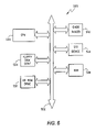
- FIG. 6 illustrates a CMOS imager containing the invention with a processing system.
- wafer and substrate are to be understood as a semiconductor-based material including silicon, silicon-on-insulator (SOI) or silicon-on-sapphire (SOS) technology, doped and undoped semiconductors, epitaxial layers of silicon supported by a base semiconductor foundation, and other semiconductor structures.
- SOI silicon-on-insulator
- SOS silicon-on-sapphire
- doped and undoped semiconductors epitaxial layers of silicon supported by a base semiconductor foundation, and other semiconductor structures.
- previous process steps may have been utilized to form regions or junctions in or over the base semiconductor structure or foundation.
- the semiconductor need not be silicon-based, but could be based on silicon-germanium, silicon-on-insulator, silicon-on-saphire, germanium, or gallium arsenide, among others.
- pixel refers to a picture element unit cell containing a photosensor and transistors for converting electromagnetic radiation to an electrical signal.
- a representative pixel is illustrated in the figures and description herein and, typically, fabrication of all pixels in an imager array will proceed simultaneously in a similar fashion.
- FIG. 2 illustrates two conventionally formed adjacent pixel cells 100 and 101 with pinned photodiodes 11 of a 4T pixel.
- the pixel cells 100 , 101 each have a single pinned photodiode 11 that is formed having a photosensitive p-n junction region comprising a p ⁇ type surface layer 4 and a n ⁇ type photodiode region 35 within a p ⁇ type region 6 .
- P ⁇ type region 6 is formed on semiconductor substrate 2 .
- Trench isolation region 8 is formed in the active layer 6 adjacent to the pinned photodiodes 11 and physically separates the two adjacent pixel cells' photodiodes 11 .
- Trench isolation region 8 is typically formed by etching trenches into the active layer 6 to provide a physical barrier between adjacent pixel cells, such as pixel cells 100 and 101 . This serves to isolate pixel cells electrically and optically from one another. The presence of trench isolation region 8 requires additional real estate in the formation of a pixel array. As FIG. 2 illustrates, below the trench isolation region 8 , a p-well 14 is present in the active layer 6 .
- the trench isolation region 8 dopant ions that are implanted in the active layer 6 surrounding the trench isolation region 8 , induce current leakage at the junction between the active device region and trench region.
- the presence of the STI region 8 also introduces stress that can have an undesirable effect on leakage.
- the dominant crystallographic planes along the bottom and sidewalls of the trench isolation region 8 possess a higher silicon density than the adjacent silicon substrate and, therefore, creates a high density of trap sites along the side and bottom of the trench isolation region 8 . These trap sites can become charged and can lead to undesired dark current.
- a minimal distance “D” needs to be maintained between the charge collection region 35 and trench isolation region 8 to avoid generating dark current and to have good substrate 2 to pinned layer 4 contact. This results in a decrease of pixel area available to the charge collection region 35 , e.g., a n-type region 35 , for electron storage which limits the capacitance of pixel cell 101 .
- FIGS. 3–5 illustrate exemplary embodiments of a semiconductor device with a pinned photodiode region constructed in accordance with the invention.
- the pinned photodiode region includes a charge collection region for collecting electrons generated from photons. It should be understood that similar reference numbers correspond to similar elements for FIGS. 3A–4 .
- the present invention provides a first pixel cell 200 a adjacent a mirror-image second pixel cell 200 b to form the structure 300 .
- the pinned photodiode 211 a of the first pixel cell 200 a shares a common p-type active region 280 , which includes p-well 214 , with the pinned photodiode 211 b of the second pixel cell 200 b .
- the common area, or active region 280 serves to isolate the pinned photodiode 211 a of the pixel cell 200 a from the pinned photodiode 211 b of the adjacent pixel cell 200 b .
- an intervening trench isolation region 8 is not required.
- the active region 280 provides good substrate to layers 204 a and 204 b contact for both pixel cells 200 a and 200 b .
- the active region 280 does not possess n ⁇ type dopant implants and includes p-type p-well region 214 .
- Pixel cell 200 a and pixel cell 200 b are isolated from other pixel cells by trench isolation regions 208 a and 208 b . However, there is no intervening trench isolation region between pixel cell 200 a and 200 b .
- layers 204 a and 204 b are preferably p-type pinned layers 204 a and 204 b.
- Active region 280 includes these p-type pinned layers 204 a and 204 b .
- the p-type pinned layers 204 a and 204 b may be implanted with p-type ions to form a p+ pinned layer 204 a and 204 b .
- p-type pinned layers 204 a and 204 b can be formed as p+ pinned layers 204 a and 204 b
- the pinned layers 204 a and 204 b can be formed as p ⁇ pinned layers 204 a and 204 b .
- pinned layers 204 a and 204 b can possess different concentrations of dopant ions from each other and pinned layers 204 a and 204 b can be formed by methods other than implantation as is known in the art.
- p-type pinned layers 204 a and 204 b can be formed by diffusion or other known methods.
- the p-type pinned layers 204 a and 204 b are preferably formed with a dopant ion concentration in the range from approximately 5.0 ⁇ 10 17 per cm 3 to approximately 5.0 ⁇ 10 19 per cm 3 .
- the p-well region 214 is preferably formed with a dopant ion concentration in the range from approximately 1.0 ⁇ 10 16 per cm 3 to approximately 5.0 ⁇ 10 17 per cm 3 .
- the n-type regions 235 a and 235 b are preferably formed with a dopant ion concentration in the range from approximately 5.0 ⁇ 10 15 per cm 3 to approximately 1.0 ⁇ 10 18 per cm 3 .
- the p+ substrate region 202 is preferably formed with a dopant ion concentration in the range from approximately 5.0 ⁇ 10 17 per cm 3 to approximately 5.0 ⁇ 10 19 per cm 3 .
- the epitaxial layers, e.g., p-type regions 206 a and 206 b are preferably formed with a dopant ion concentration in the range from approximately 1.0 ⁇ 10 14 per cm 3 to approximately 1.0 ⁇ 10 16 per cm 3 .
- the resulting structure 300 enables a CMOS image device to be packaged to a smaller dimension than conventionally formed CMOS image devices, since adjacent pixel cells 200 a , 200 b are formed without the presence of an intervening trench isolation region and share a common area 280 which includes p-well region 214 and p-type pinned layers 204 a and 204 b . Further, a CMOS imager employing adjacent pixels 200 a and 200 b , will not generate as much dark current as some prior isolated pixel cells since the number of trench isolation regions for the imager is reduced.
- pinned photodiode's capacitance for pixel cells 200 a and 200 b can be increased, if desired.
- pinned photodiode's 211 a and 211 b can be formed with larger charge collection regions 235 a and 235 b since the trench isolation region that typically separates adjacent pinned photodiodes is not present.
- CMOS imager including, for example, a three-transistor (3T) cell which differs from the 4T cell in the omission of a transfer transistor gate, illustrated and describe in FIG. 5 .
- pinned photodiode 211 a and 211 b share a common active region 280 , which includes p-well 214 and p-type pinned layers 204 a and 204 b , of the 4T FIG. 3 embodiment, pinned photodiode 211 a sends electrons to transfer transistor gate 260 a and pinned photodiode 211 b , sends electrons to transfer transistor gate 260 b .
- pinned photodiode 211 a sends electrons to floating diffusion region 210 a and pinned photodiode 211 b sends electrons to floating diffusion region 210 b.
- a method for forming structure 300 will now be explained in reference to FIGS. 4A–4F .
- Elements designated with an “a” belong to the first pixel cell 200 and elements designated with a “b” belong to the second pixel cell 201 .
- FIG. 4A illustrates a substrate 202 along a diagrammatic side sectional view of a CMOS image structure formed in accordance with a first embodiment of the present invention.
- the substrate 202 is a silicon substrate formed to a predetermined thickness.
- the invention has equal utility with other semiconductor substrates.
- the substrate 202 is shared by the two pixel cells 200 a and 200 b .
- the substrate region 202 is preferably formed with a p-type dopant ion concentration in the range from approximately 5.0 ⁇ 10 17 per cm 3 to approximately 5.0 ⁇ 10 19 per cm 3 . It should be appreciated that the substrate region 202 can have p-type dopant ions added at a subsequent processing step.
- FIG. 4B illustrates transfer transistor gate stacks 260 a , 260 b formed over the silicon substrate 202 .
- the transfer transistor gate stacks 260 a , 260 b comprise a first gate oxide layer 231 a , 231 b of grown or deposited silicon oxide on the silicon substrate 202 , a conductive layer 232 a , 232 b of doped polysilicon or other suitable conductor material, and a second insulating layer 233 a , 233 b which may be formed of, for example, silicon oxide (silicon dioxide), nitride (silicon nitride), oxynitride (silicon oxynitride), ON (oxide-nitride), NO (nitride-oxide), or ONO (oxide-nitride-oxide), among others.
- the transfer transistor gate stack 260 a can comprise a different material, a different thickness, and a different shape from the transfer transistor gate stack 260 b.
- the first and second insulating layers 231 a , 231 b , 233 a , and 233 b , and the conductive layer 232 a , 232 b may be formed by conventional deposition methods, for example, chemical vapor deposition (CVD) or plasma enhanced chemical vapor deposition (PECVD), among many others. Further, it should be appreciated that the first and second insulating layers 231 a , 233 a and the conductive layer 232 a can comprise different materials, be made to different thicknesses, or even be a different shape from the first and second insulating layers 231 b , 233 b and the conductive layer 232 b of the second pixel cell 200 b.
- CVD chemical vapor deposition
- PECVD plasma enhanced chemical vapor deposition
- a silicide layer may be also formed in the transfer transistor gate stacks 260 a , 260 b , between the conductive layers 232 a , 232 b and the second insulating layers 233 a , 233 b .
- the gate structures of all other transistors (not illustrated) in the imager circuit design may have this additionally formed silicide layer.
- This silicide layer may be titanium silicide, tungsten silicide, cobalt silicide, molybdenum silicide, or tantalum silicide, among others.
- the silicide layer could also be a barrier layer/refractory metal such as TiN/W or WN X /W, or it could be entirely formed of WN X , among others.
- FIG. 4C illustrates insulating sidewall spacers 234 a , 234 b formed on the sides of the transfer transistor gate stacks 260 a , 260 b through conventional methods.
- the sidewall spacers 234 a , 234 b may be formed, for example, of silicon dioxide, silicon nitride, silicon oxynitride, ON, NO, ONO or TEOS, among others.
- additional transistors can be provided such as reset transistors 250 a , 250 b , source follower transistors (not shown), and row select transistors (not shown) as described above in forming the transfer transistors 260 a , 260 b.
- trench isolation regions 208 a , 208 b are formed within the substrate 202 to separate pixel cells 200 a and 200 b from adjacent pixel cells or structures.
- the trench isolation regions 208 a , 208 b are filled with a dielectric material, which may be an oxide material, for example a silicon oxide such as SiO or SiO 2 , a thermally grown oxide, oxynitride, a nitride material such as silicon nitride, silicon carbide, a high temperature polymer, or other suitable dielectric materials.
- the dielectric may be also formed of any combination of oxide/nitride, nitride/oxide and oxide/nitride/oxide materials.
- the trench isolation regions 208 a , 208 b are shallow trench isolation regions and the dielectric material is a high density plasma (HDP) oxide, a material which has a high ability to effectively fill narrow trenches.
- HDP high density plasma
- the isolation regions 208 a , 208 b are described as being formed after gate stacks 260 a , 260 b are formed, it should be appreciated that the trench isolation regions 208 a , 208 b can be formed prior to gate stacks 260 a , 260 b formation or even in a later step, such as after formation of pinned photodiodes 211 a , 211 b.
- a thin insulating layer may be formed on the sidewalls and bottoms of the shallow trench isolation regions before the filling of the trenches with the dielectric material which, as noted, is preferably a high density plasma (HDP) oxide.
- the thin insulating layer may be formed of an oxide or of silicon nitride or an oxide/nitride combination, for example, to aid in smoothing out the corners in the bottom of the trench and to reduce the amount of stress in the dielectric material used to later fill in the trenches.
- p-n-p pinned photodiode 211 a is formed by regions 204 a , 206 a , and 235 a .
- Regions 204 a , 206 a , and 235 a are formed to a predetermined dopant concentration.
- region 204 a is formed to have a p+ dopant concentration.
- region 204 a is described as a p+ type region, region 204 a can also be a p-type region.
- Region 206 a is formed to have a p ⁇ type dopant concentration that is less than the dopant concentration of region 204 a .
- Region 235 a is formed to have a n ⁇ type dopant concentration.
- Photodiode 211 b also a p-n-p pinned photodiode, is formed by regions 204 b , 206 b , and 235 b .
- regions 204 b , 206 b , and 235 b are formed in a similar manner to regions 204 a , 206 a , and 235 a.
- Active region 280 is the active area between the two adjacent pixel cells 200 a and 200 b which includes p-well 214 and p-type pinned surface layers 204 a and 204 b .
- the active region 280 provides a good surface to substrate contact e.g., p-type pinned surface layer 204 a through p-well 214 to p ⁇ type region 206 a to p-type substrate 202 , for pixel cell 200 a and p-type pinned surface layer 204 b through p-well 214 to p ⁇ type region 206 b to p-type substrate 202 , for pixel cell 200 b .
- the p-well region 214 is preferably formed with a dopant ion concentration in the range from approximately 1.0 ⁇ 10 16 per cm 3 to approximately 5.0 ⁇ 10 17 per cm 3 .
- the p-well region 214 can be formed by implantation or other methods well known in the art.
- the p ⁇ type doped regions or wells 206 a and 206 b are formed in the areas of the substrate 202 directly beneath the active area of the pixel cells 200 a and 200 b by conducting a dopant implantation with a dopant of a first conductivity type, which for exemplary purposes is p ⁇ type.
- p ⁇ type doped regions 206 a and 206 b can be formed by methods other than ion implantation.
- the p-type doped layers or wells 206 a , 206 b may be formed subsequent to the formation of trench isolation regions 208 a , 208 b and of the transfer transistor gate stacks 260 a , 260 b .
- the p-type doped layers or wells 206 a and 206 b may also be formed prior to the formation of trench isolation regions 208 a , 208 b .
- the epitaxial layers, e.g., p ⁇ type regions 206 a and 206 b are preferably formed with a dopant ion concentration in the range from approximately 1.0 ⁇ 10 14 per cm 3 to approximately 1.0 ⁇ 10 16 per cm 3 .
- the n ⁇ type regions 235 a and 235 b are formed by implanting dopants of a second conductivity type, which for exemplary purposes is n-type, in the area of the substrate 202 directly beneath the active area of the pixel cells 200 a and 200 b .
- the implanted n-doped regions 235 a and 235 b form a photosensitive charge storage region for collecting photogenerated electrons for the pixel cells 200 a and 200 b .
- the n ⁇ type regions 235 a and 235 b are preferably formed with a dopant ion concentration in the range from approximately 5.0 ⁇ 10 15 per cm 3 to approximately 1.0 ⁇ 10 18 per cm 3 . It should be appreciated that the n ⁇ type regions 235 a and 235 b can be formed with by methods other than implantation as is known in the art.
- n ⁇ type regions 235 a and 235 b are not connected nor touching each other.
- Active region 280 is present to at least some degree between the n ⁇ type regions 235 a and 235 b of the two adjacent pixel cells 200 a and 200 b .
- the presence of the active region 280 which includes p-well 214 and p-type pinned surface layers 204 a and 204 b , serves to isolate the two adjacent photodiodes 211 a and 211 b from each other.
- active region 280 is commonly shared by the adjacent pixel cells 200 a and 200 b .
- Active region 280 should also not contain the dopant ions used to form charge collection regions 235 a and 235 b , e.g., n-type dopant ions.
- the p ⁇ type pinned surface layers 204 a and 204 b are also formed by conducting a dopant implantation with a dopant of the first conductivity type, which for exemplary purposes is p ⁇ type, so that p ⁇ type ions are implanted into the area of the substrate 202 over the implanted n ⁇ type regions 235 a and 235 b and between the transfer transistor gates 460 a and 460 b .
- the p ⁇ type pinned layers 204 a and 204 b are preferably formed with a dopant ion concentration in the range from approximately 5.0 ⁇ 10 17 per cm 3 to approximately 5.0 ⁇ 10 19 per cm 3 . It should be appreciated that the p ⁇ type pinned surface layers 204 a and 204 b can be formed with by methods other than implantation as is known in the art.
- the pixel cells 200 a and 200 b can have regions of different dopant ion concentrations from each other.
- n-type region 235 a can possess a different dopant ion concentration from n-type region 235 b .
- the p ⁇ type region 206 a can have a different dopant ion concentration from p ⁇ type region 206 b.
- regions 204 a , 206 a , and 235 a are described as being formed simultaneously with regions 204 b , 206 b , and 235 b , it should be appreciated that these regions can be formed at different times, with different dopant concentrations, and even different depths from each other so long as active region 280 , which includes p-well 214 , is shared by adjacent pixel cells 200 a and 200 b.
- FIG. 4E illustrates forming a n ⁇ type floating diffusion region 210 a located adjacent the transfer transistor gate stack 260 a and opposite the n ⁇ type doped region 235 a of the p-n-p photodiode 211 a .
- n ⁇ type floating diffusion region 210 b is formed adjacent the transfer transistor gate stack 260 b and opposite the n ⁇ type doped region 235 b of the p-n-p photodiode 211 b .
- the transfer transistor gate stack 260 a transfers charge accumulated in the charge collection region 235 a of the pinned photodiode 211 a to the floating diffusion region 210 a for example.
- FIG. 4E illustrates forming source/drain regions 205 a and 205 b for reset transistors 250 a and 250 b .
- the source/drain region 205 a can have a different dopant concentration from the floating diffusion region 210 a of reset transistor 250 a .
- the source/drain region 205 b can have a different dopant concentration from the floating diffusion region 210 b of the reset transistor 250 b.
- the dopant concentrations and dopant ions used for pixel cell 200 a can be different from dopant concentrations and dopant ions used in pixel cell 200 b .
- floating diffusion regions 210 a , 210 b , source/drain regions 205 a , 205 b , and pinned photodiodes 211 a , 211 b can possess different dopant concentrations and can be formed from different dopant ions.
- the n ⁇ type dopant ions used for doping different regions of pixel cell 200 a and pixel cell 200 b may comprise phosphorus, arsenic, antimony, or other n ⁇ type dopant ions known in the art.
- the p ⁇ type dopant ions used for doping different regions of pixel cell 200 a and pixel cell 200 b may comprise boron, beryllium, indium, magnesium, or other p ⁇ type dopant ions known in the art.
- the CMOS pixel structure 300 is then processed according to known methods to produce an operative pixel.
- a transparent insulating layer 299 a , 299 b can be provided over the transfer transistors 260 a , 260 b and reset transistors 250 a , and 250 b .
- An opening can be formed and a metal conductor 215 a can be used to connect the floating diffusion region 210 a with a source follower transistor (not shown) and row select transistor (not shown).
- an opening can be formed and a metal conductor 215 b can be used to connect the floating diffusion region 210 b with a source follower transistor (not shown) and row select transistor (not shown).
- pinned photodiodes 211 a , 211 b can be formed with a greater charge collection region 235 a , 235 b .
- structure 300 has a greater capacitance than previous prior art structures as illustrated in FIG. 2 .
- a minimum distance D needed to be maintained from the trench isolation region 8 to avoid generating dark current and to have good p-surface 4 to p-type region 6 and p-type substrate 2 contact.
- active area region 280 which includes p-well 214 and p ⁇ type pinned surface layers 204 a and 204 b , provides good p-type pinned surface 204 a , 204 b through p-well region 214 to p-type region 206 a , 206 b to p-type substrate 202 contact.
- Structure 300 also does not generate the dark current associated with the presence of a trench isolation region.
- the structure 300 depicted in FIG. 3A and methods of forming such a structure depicted in FIGS. 4A–4F relate to a 4T pixel which utilizes transfer transistors 260 and 260 b for gating charge from the pinned photodiodes 211 a and 211 b to the floating diffusion regions 210 a and 210 b .
- FIG. 5 illustrates another exemplary embodiment of the present invention in a 3T pixel.
- the charge collection regions 435 a and 435 b are connected with the floating diffusion regions 410 a and 410 b respectively, and the transfer transistors 260 a and 260 b of FIG. 3 are omitted.
- the structure 600 shown in FIG. 5 is the same as structure 300 in FIG. 3 .
- adjacent pixels 400 a and 400 b share a common active region 480 with p-well 414 .
- the methods of forming structure 600 is similar to the methods described above for forming structure 300 .
- the transfer transistors 260 a , 260 b of FIG. 3 are not provided in this embodiment.
- pinned photodiode 411 a is connected to floating diffusion region 410 a for pixel cell 400 a .
- pinned photodiode 411 b is connected to floating diffusion region 410 b for pixel cell 400 b.
- the CMOS pixel structure 600 is then processed according to known methods to produce an operative pixel.
- a transparent insulating layer 499 can be provided over the reset transistors 450 a and 450 b .
- An opening can be formed for pixel cell 400 a in the insulating layer 499 a , 499 b and a metal conductor 415 a can be used to connect the floating diffusion region 410 a with a source follower transistor (not shown) and row select transistor (not shown).
- an opening can be formed for pixel cell 400 b and a metal conductor 415 b can be used to connect the floating diffusion region 410 b with a source follower transistor (not shown) and row select transistor (not shown).
- structure 300 or 600 enables a CMOS (or PMOS) image device to be formed with smaller dimensions. Specifically, the absence of a trench isolation region separating adjacent pixel cells allows more pixel cells to be formed on a semiconductor substrate for a given device. The pixel cell size is smaller since adjacent pixel cells share a common active region. In addition, reducing the number of trench isolation regions for a given CMOS or PMOS image device, can also reduce the generation of dark current since the presence of isolation regions can generate dark current.
- the structures 300 and 600 described above, can also provide the benefit of increasing the pinned photodiode's capacitance for each pixel cell.
- a pixel cell can possess a larger photodiode collection region with the absence of a trench isolation region; thus, increasing the pixel cell's charge collection region and therefore its capacitance. Moreover, good p-type surface to p-type substrate contact is maintained through the common active region.
- a typical processor based system which includes a CMOS imager device 542 having a pixel array in which the pixels are constructed according to the present invention is illustrated generally at 500 in FIG. 6 .
- the imager device produces an output image from signals supplied from the pixel array.
- a processor based system is exemplary of a system receiving the output of a CMOS imager device. Without being limiting, such a system could include a computer system, camera system, scanner, machine vision system, vehicle navigation system, video phone, surveillance system, auto focus system, star tracker system, motion detection system, image stabilization system, all of which can utilize the present invention.
- a processor based system such as a computer system, for example generally comprises a central processing unit (CPU) 544 , for example, a microprocessor, that communicates with an input/output (I/O) device 546 over a bus 552 .
- the CMOS imager device 542 also communicates with the system over bus 552 or other communication link.
- the computer system 500 also includes random access memory (RAM) 548 , and, in the case of a computer system may include peripheral devices such as a floppy disk drive 554 and a compact disk (CD) ROM drive 556 which also communicate with CPU 544 over the bus 552 . It may also be desirable to integrate the processor 554 , CMOS imager device 542 and memory 548 on a single IC chip.
- the invention has been described with reference to pixels employing n ⁇ channel transistors. However, it should be understood that the invention is not so limited and may be employed in pixels have p ⁇ channel devices formed within a n ⁇ type substrate.
Abstract
Description
Claims (33)
Priority Applications (2)
| Application Number | Priority Date | Filing Date | Title |
|---|---|---|---|
| US10/461,802 US7009227B2 (en) | 2003-06-16 | 2003-06-16 | Photodiode structure and image pixel structure |
| US11/086,347 US7244646B2 (en) | 2003-06-16 | 2005-03-23 | Pixel design to improve photodiode capacitance and method of forming same |
Applications Claiming Priority (1)
| Application Number | Priority Date | Filing Date | Title |
|---|---|---|---|
| US10/461,802 US7009227B2 (en) | 2003-06-16 | 2003-06-16 | Photodiode structure and image pixel structure |
Related Child Applications (1)
| Application Number | Title | Priority Date | Filing Date |
|---|---|---|---|
| US11/086,347 Division US7244646B2 (en) | 2003-06-16 | 2005-03-23 | Pixel design to improve photodiode capacitance and method of forming same |
Publications (2)
| Publication Number | Publication Date |
|---|---|
| US20040262646A1 US20040262646A1 (en) | 2004-12-30 |
| US7009227B2 true US7009227B2 (en) | 2006-03-07 |
Family
ID=33538975
Family Applications (2)
| Application Number | Title | Priority Date | Filing Date |
|---|---|---|---|
| US10/461,802 Expired - Lifetime US7009227B2 (en) | 2003-06-16 | 2003-06-16 | Photodiode structure and image pixel structure |
| US11/086,347 Expired - Lifetime US7244646B2 (en) | 2003-06-16 | 2005-03-23 | Pixel design to improve photodiode capacitance and method of forming same |
Family Applications After (1)
| Application Number | Title | Priority Date | Filing Date |
|---|---|---|---|
| US11/086,347 Expired - Lifetime US7244646B2 (en) | 2003-06-16 | 2005-03-23 | Pixel design to improve photodiode capacitance and method of forming same |
Country Status (1)
| Country | Link |
|---|---|
| US (2) | US7009227B2 (en) |
Cited By (27)
| Publication number | Priority date | Publication date | Assignee | Title |
|---|---|---|---|---|
| US20060181625A1 (en) * | 2005-01-24 | 2006-08-17 | Korea Advanced Institute Of Science And Technology | CMOS image sensor with wide dynamic range |
| US20070012966A1 (en) * | 2005-07-13 | 2007-01-18 | Won-Je Park | Image Sensors and Methods of Fabricating Same |
| US20070023799A1 (en) * | 2005-08-01 | 2007-02-01 | Micro Technology, Inc. | Structure and method for building a light tunnel for use with imaging devices |
| US20080217718A1 (en) * | 2007-03-06 | 2008-09-11 | Micron Technology, Inc. | Method, apparatus, and system to reduce ground resistance in a pixel array |
| US20080217720A1 (en) * | 2007-03-09 | 2008-09-11 | Micron Technology, Inc. | Dual isolation for image sensors |
| US20080225144A1 (en) * | 2007-03-12 | 2008-09-18 | Micron Technology, Inc. | Multi-purpose image sensor circuits, imager, system and method of operation |
| US20080257187A1 (en) * | 2007-04-18 | 2008-10-23 | Micron Technology, Inc. | Methods of forming a stamp, methods of patterning a substrate, and a stamp and a patterning system for same |
| US20080277693A1 (en) * | 2007-05-10 | 2008-11-13 | Micron Technology, Inc. | Imager element, device and system with recessed transfer gate |
| US20080315263A1 (en) * | 2007-06-20 | 2008-12-25 | Micron Technology, Inc. | Imager pixel structure and circuit |
| US20080315270A1 (en) * | 2007-06-21 | 2008-12-25 | Micron Technology, Inc. | Multilayer antireflection coatings, structures and devices including the same and methods of making the same |
| US20090166793A1 (en) * | 2007-12-28 | 2009-07-02 | Joon Hwang | Image sensor and method for manufacturing the same |
| US20100102415A1 (en) * | 2008-10-28 | 2010-04-29 | Micron Technology, Inc. | Methods for selective permeation of self-assembled block copolymers with metal oxides, methods for forming metal oxide structures, and semiconductor structures including same |
| US8557128B2 (en) | 2007-03-22 | 2013-10-15 | Micron Technology, Inc. | Sub-10 nm line features via rapid graphoepitaxial self-assembly of amphiphilic monolayers |
| US8609221B2 (en) | 2007-06-12 | 2013-12-17 | Micron Technology, Inc. | Alternating self-assembling morphologies of diblock copolymers controlled by variations in surfaces |
| US8633112B2 (en) | 2008-03-21 | 2014-01-21 | Micron Technology, Inc. | Thermal anneal of block copolymer films with top interface constrained to wet both blocks with equal preference |
| US8641914B2 (en) | 2008-03-21 | 2014-02-04 | Micron Technology, Inc. | Methods of improving long range order in self-assembly of block copolymer films with ionic liquids |
| US8642157B2 (en) | 2008-02-13 | 2014-02-04 | Micron Technology, Inc. | One-dimensional arrays of block copolymer cylinders and applications thereof |
| US8753738B2 (en) | 2007-03-06 | 2014-06-17 | Micron Technology, Inc. | Registered structure formation via the application of directed thermal energy to diblock copolymer films |
| US8785559B2 (en) | 2007-06-19 | 2014-07-22 | Micron Technology, Inc. | Crosslinkable graft polymer non-preferentially wetted by polystyrene and polyethylene oxide |
| US8900963B2 (en) | 2011-11-02 | 2014-12-02 | Micron Technology, Inc. | Methods of forming semiconductor device structures, and related structures |
| US8993088B2 (en) | 2008-05-02 | 2015-03-31 | Micron Technology, Inc. | Polymeric materials in self-assembled arrays and semiconductor structures comprising polymeric materials |
| US8999492B2 (en) | 2008-02-05 | 2015-04-07 | Micron Technology, Inc. | Method to produce nanometer-sized features with directed assembly of block copolymers |
| US9087699B2 (en) | 2012-10-05 | 2015-07-21 | Micron Technology, Inc. | Methods of forming an array of openings in a substrate, and related methods of forming a semiconductor device structure |
| US9129872B2 (en) | 2012-09-20 | 2015-09-08 | Semiconductor Components Industries, Llc | Imaging pixels with improved photodiode structures |
| US9142420B2 (en) | 2007-04-20 | 2015-09-22 | Micron Technology, Inc. | Extensions of self-assembled structures to increased dimensions via a “bootstrap” self-templating method |
| US9177795B2 (en) | 2013-09-27 | 2015-11-03 | Micron Technology, Inc. | Methods of forming nanostructures including metal oxides |
| US9229328B2 (en) | 2013-05-02 | 2016-01-05 | Micron Technology, Inc. | Methods of forming semiconductor device structures, and related semiconductor device structures |
Families Citing this family (13)
| Publication number | Priority date | Publication date | Assignee | Title |
|---|---|---|---|---|
| KR100614653B1 (en) * | 2004-11-18 | 2006-08-22 | 삼성전자주식회사 | CMOS Image Sensor Capable Of A Global Exposure Without White Spot And Overflow And Method Of Fabricating The Same |
| US8686481B2 (en) * | 2005-04-29 | 2014-04-01 | Trixell | Semiconductor device with an image sensor and method for the manufacturing of such a device |
| KR100632954B1 (en) * | 2005-05-06 | 2006-10-12 | 삼성전자주식회사 | Cmos image sensor and method of fabricating the same |
| US7432121B2 (en) * | 2005-05-24 | 2008-10-07 | Micron Technology, Inc. | Isolation process and structure for CMOS imagers |
| US7608874B2 (en) * | 2006-03-17 | 2009-10-27 | Sharp Laboratories Of America, Inc. | Fully isolated photodiode stack |
| US20080243991A1 (en) * | 2007-03-29 | 2008-10-02 | Ryan Thomas A | Content Purchase and Transfer Management for Reader Device |
| JP4350768B2 (en) | 2007-04-16 | 2009-10-21 | キヤノン株式会社 | Photoelectric conversion device and imaging device |
| US7924333B2 (en) | 2007-08-17 | 2011-04-12 | Aptina Imaging Corporation | Method and apparatus providing shared pixel straight gate architecture |
| US7989749B2 (en) * | 2007-10-05 | 2011-08-02 | Aptina Imaging Corporation | Method and apparatus providing shared pixel architecture |
| US20090272881A1 (en) * | 2008-05-05 | 2009-11-05 | Xiangli Li | Apparatus, method, and system providing pixel having increased fill factor |
| JP4759590B2 (en) | 2008-05-09 | 2011-08-31 | キヤノン株式会社 | Photoelectric conversion device and imaging system using the same |
| US9349785B2 (en) | 2013-11-27 | 2016-05-24 | Taiwan Semiconductor Manufacturing Co., Ltd. | Formation of semiconductor device with resistors |
| CN105405918B (en) * | 2014-09-10 | 2017-06-06 | 中芯国际集成电路制造(上海)有限公司 | A kind of photodiode preparation method |
Citations (7)
| Publication number | Priority date | Publication date | Assignee | Title |
|---|---|---|---|---|
| US5286990A (en) * | 1991-08-19 | 1994-02-15 | Texas Instruments Incorporated | Top buss virtual phase frame interline transfer CCD image sensor |
| US6140630A (en) * | 1998-10-14 | 2000-10-31 | Micron Technology, Inc. | Vcc pump for CMOS imagers |
| US6204524B1 (en) * | 1999-07-14 | 2001-03-20 | Micron Technology, Inc. | CMOS imager with storage capacitor |
| US6310366B1 (en) * | 1999-06-16 | 2001-10-30 | Micron Technology, Inc. | Retrograde well structure for a CMOS imager |
| US6326652B1 (en) * | 1999-06-18 | 2001-12-04 | Micron Technology, Inc., | CMOS imager with a self-aligned buried contact |
| US6333205B1 (en) * | 1999-08-16 | 2001-12-25 | Micron Technology, Inc. | CMOS imager with selectively silicided gates |
| US6376868B1 (en) * | 1999-06-15 | 2002-04-23 | Micron Technology, Inc. | Multi-layered gate for a CMOS imager |
Family Cites Families (5)
| Publication number | Priority date | Publication date | Assignee | Title |
|---|---|---|---|---|
| US5903021A (en) * | 1997-01-17 | 1999-05-11 | Eastman Kodak Company | Partially pinned photodiode for solid state image sensors |
| JP3554483B2 (en) * | 1998-04-22 | 2004-08-18 | シャープ株式会社 | CMOS solid-state imaging device |
| US6489643B1 (en) * | 1998-06-27 | 2002-12-03 | Hynix Semiconductor Inc. | Photodiode having a plurality of PN junctions and image sensor having the same |
| KR20010061351A (en) * | 1999-12-28 | 2001-07-07 | 박종섭 | CMOS image sensor having photodiode coupled capacitor |
| US6372537B1 (en) * | 2000-03-17 | 2002-04-16 | Taiwan Semiconductor Manufacturing Company | Pinned photodiode structure in a 3T active pixel sensor |
-
2003
- 2003-06-16 US US10/461,802 patent/US7009227B2/en not_active Expired - Lifetime
-
2005
- 2005-03-23 US US11/086,347 patent/US7244646B2/en not_active Expired - Lifetime
Patent Citations (7)
| Publication number | Priority date | Publication date | Assignee | Title |
|---|---|---|---|---|
| US5286990A (en) * | 1991-08-19 | 1994-02-15 | Texas Instruments Incorporated | Top buss virtual phase frame interline transfer CCD image sensor |
| US6140630A (en) * | 1998-10-14 | 2000-10-31 | Micron Technology, Inc. | Vcc pump for CMOS imagers |
| US6376868B1 (en) * | 1999-06-15 | 2002-04-23 | Micron Technology, Inc. | Multi-layered gate for a CMOS imager |
| US6310366B1 (en) * | 1999-06-16 | 2001-10-30 | Micron Technology, Inc. | Retrograde well structure for a CMOS imager |
| US6326652B1 (en) * | 1999-06-18 | 2001-12-04 | Micron Technology, Inc., | CMOS imager with a self-aligned buried contact |
| US6204524B1 (en) * | 1999-07-14 | 2001-03-20 | Micron Technology, Inc. | CMOS imager with storage capacitor |
| US6333205B1 (en) * | 1999-08-16 | 2001-12-25 | Micron Technology, Inc. | CMOS imager with selectively silicided gates |
Cited By (58)
| Publication number | Priority date | Publication date | Assignee | Title |
|---|---|---|---|---|
| US20060181625A1 (en) * | 2005-01-24 | 2006-08-17 | Korea Advanced Institute Of Science And Technology | CMOS image sensor with wide dynamic range |
| US7619674B2 (en) * | 2005-01-24 | 2009-11-17 | Korea Advanced Institute Of Science And Technology | CMOS image sensor with wide dynamic range |
| US20070012966A1 (en) * | 2005-07-13 | 2007-01-18 | Won-Je Park | Image Sensors and Methods of Fabricating Same |
| US7772624B2 (en) * | 2005-07-13 | 2010-08-10 | Samsung Electronics Co., Ltd. | Image sensors and methods of fabricating same |
| US20070023799A1 (en) * | 2005-08-01 | 2007-02-01 | Micro Technology, Inc. | Structure and method for building a light tunnel for use with imaging devices |
| US20080217718A1 (en) * | 2007-03-06 | 2008-09-11 | Micron Technology, Inc. | Method, apparatus, and system to reduce ground resistance in a pixel array |
| US7728279B2 (en) | 2007-03-06 | 2010-06-01 | Aptina Imaging Corporation | Methods, devices, and systems related to pixel arrays |
| US7459668B2 (en) | 2007-03-06 | 2008-12-02 | Micron Technology, Inc. | Method, apparatus, and system to reduce ground resistance in a pixel array |
| US8753738B2 (en) | 2007-03-06 | 2014-06-17 | Micron Technology, Inc. | Registered structure formation via the application of directed thermal energy to diblock copolymer films |
| US20090067702A1 (en) * | 2007-03-06 | 2009-03-12 | Micron Technology, Inc. | Methods, devices, and systems related to pixel arrays |
| US20080217720A1 (en) * | 2007-03-09 | 2008-09-11 | Micron Technology, Inc. | Dual isolation for image sensors |
| US7642608B2 (en) | 2007-03-09 | 2010-01-05 | Aptina Imaging Corporation | Dual isolation for image sensors |
| US20080225144A1 (en) * | 2007-03-12 | 2008-09-18 | Micron Technology, Inc. | Multi-purpose image sensor circuits, imager, system and method of operation |
| US7724293B2 (en) | 2007-03-12 | 2010-05-25 | Aptina Imaging Corporation | Multi-purpose image sensor circuits, imager, system and method of operation |
| US8557128B2 (en) | 2007-03-22 | 2013-10-15 | Micron Technology, Inc. | Sub-10 nm line features via rapid graphoepitaxial self-assembly of amphiphilic monolayers |
| US8784974B2 (en) | 2007-03-22 | 2014-07-22 | Micron Technology, Inc. | Sub-10 NM line features via rapid graphoepitaxial self-assembly of amphiphilic monolayers |
| US8801894B2 (en) | 2007-03-22 | 2014-08-12 | Micron Technology, Inc. | Sub-10 NM line features via rapid graphoepitaxial self-assembly of amphiphilic monolayers |
| US9768021B2 (en) | 2007-04-18 | 2017-09-19 | Micron Technology, Inc. | Methods of forming semiconductor device structures including metal oxide structures |
| US8956713B2 (en) | 2007-04-18 | 2015-02-17 | Micron Technology, Inc. | Methods of forming a stamp and a stamp |
| US20080257187A1 (en) * | 2007-04-18 | 2008-10-23 | Micron Technology, Inc. | Methods of forming a stamp, methods of patterning a substrate, and a stamp and a patterning system for same |
| US7959975B2 (en) | 2007-04-18 | 2011-06-14 | Micron Technology, Inc. | Methods of patterning a substrate |
| US9276059B2 (en) | 2007-04-18 | 2016-03-01 | Micron Technology, Inc. | Semiconductor device structures including metal oxide structures |
| US9142420B2 (en) | 2007-04-20 | 2015-09-22 | Micron Technology, Inc. | Extensions of self-assembled structures to increased dimensions via a “bootstrap” self-templating method |
| US20080277693A1 (en) * | 2007-05-10 | 2008-11-13 | Micron Technology, Inc. | Imager element, device and system with recessed transfer gate |
| US7768047B2 (en) | 2007-05-10 | 2010-08-03 | Micron Technology, Inc. | Imager element, device and system with recessed transfer gate |
| US8609221B2 (en) | 2007-06-12 | 2013-12-17 | Micron Technology, Inc. | Alternating self-assembling morphologies of diblock copolymers controlled by variations in surfaces |
| US9257256B2 (en) | 2007-06-12 | 2016-02-09 | Micron Technology, Inc. | Templates including self-assembled block copolymer films |
| US8785559B2 (en) | 2007-06-19 | 2014-07-22 | Micron Technology, Inc. | Crosslinkable graft polymer non-preferentially wetted by polystyrene and polyethylene oxide |
| US7642580B2 (en) | 2007-06-20 | 2010-01-05 | Apitina Imaging Corporation | Imager pixel structure and circuit |
| US20080315263A1 (en) * | 2007-06-20 | 2008-12-25 | Micron Technology, Inc. | Imager pixel structure and circuit |
| US20080315270A1 (en) * | 2007-06-21 | 2008-12-25 | Micron Technology, Inc. | Multilayer antireflection coatings, structures and devices including the same and methods of making the same |
| US8551808B2 (en) | 2007-06-21 | 2013-10-08 | Micron Technology, Inc. | Methods of patterning a substrate including multilayer antireflection coatings |
| US8294139B2 (en) | 2007-06-21 | 2012-10-23 | Micron Technology, Inc. | Multilayer antireflection coatings, structures and devices including the same and methods of making the same |
| US8089106B2 (en) * | 2007-12-28 | 2012-01-03 | Dongbu Hitek Co., Ltd. | Image sensor and method for manufacturing the same |
| US20090166793A1 (en) * | 2007-12-28 | 2009-07-02 | Joon Hwang | Image sensor and method for manufacturing the same |
| US10005308B2 (en) | 2008-02-05 | 2018-06-26 | Micron Technology, Inc. | Stamps and methods of forming a pattern on a substrate |
| US10828924B2 (en) | 2008-02-05 | 2020-11-10 | Micron Technology, Inc. | Methods of forming a self-assembled block copolymer material |
| US11560009B2 (en) | 2008-02-05 | 2023-01-24 | Micron Technology, Inc. | Stamps including a self-assembled block copolymer material, and related methods |
| US8999492B2 (en) | 2008-02-05 | 2015-04-07 | Micron Technology, Inc. | Method to produce nanometer-sized features with directed assembly of block copolymers |
| US8642157B2 (en) | 2008-02-13 | 2014-02-04 | Micron Technology, Inc. | One-dimensional arrays of block copolymer cylinders and applications thereof |
| US8633112B2 (en) | 2008-03-21 | 2014-01-21 | Micron Technology, Inc. | Thermal anneal of block copolymer films with top interface constrained to wet both blocks with equal preference |
| US10153200B2 (en) | 2008-03-21 | 2018-12-11 | Micron Technology, Inc. | Methods of forming a nanostructured polymer material including block copolymer materials |
| US11282741B2 (en) | 2008-03-21 | 2022-03-22 | Micron Technology, Inc. | Methods of forming a semiconductor device using block copolymer materials |
| US8641914B2 (en) | 2008-03-21 | 2014-02-04 | Micron Technology, Inc. | Methods of improving long range order in self-assembly of block copolymer films with ionic liquids |
| US9682857B2 (en) | 2008-03-21 | 2017-06-20 | Micron Technology, Inc. | Methods of improving long range order in self-assembly of block copolymer films with ionic liquids and materials produced therefrom |
| US9315609B2 (en) | 2008-03-21 | 2016-04-19 | Micron Technology, Inc. | Thermal anneal of block copolymer films with top interface constrained to wet both blocks with equal preference |
| US8993088B2 (en) | 2008-05-02 | 2015-03-31 | Micron Technology, Inc. | Polymeric materials in self-assembled arrays and semiconductor structures comprising polymeric materials |
| US8669645B2 (en) | 2008-10-28 | 2014-03-11 | Micron Technology, Inc. | Semiconductor structures including polymer material permeated with metal oxide |
| US8097175B2 (en) | 2008-10-28 | 2012-01-17 | Micron Technology, Inc. | Method for selectively permeating a self-assembled block copolymer, method for forming metal oxide structures, method for forming a metal oxide pattern, and method for patterning a semiconductor structure |
| US20100102415A1 (en) * | 2008-10-28 | 2010-04-29 | Micron Technology, Inc. | Methods for selective permeation of self-assembled block copolymers with metal oxides, methods for forming metal oxide structures, and semiconductor structures including same |
| US8900963B2 (en) | 2011-11-02 | 2014-12-02 | Micron Technology, Inc. | Methods of forming semiconductor device structures, and related structures |
| US9431605B2 (en) | 2011-11-02 | 2016-08-30 | Micron Technology, Inc. | Methods of forming semiconductor device structures |
| US9129872B2 (en) | 2012-09-20 | 2015-09-08 | Semiconductor Components Industries, Llc | Imaging pixels with improved photodiode structures |
| US9087699B2 (en) | 2012-10-05 | 2015-07-21 | Micron Technology, Inc. | Methods of forming an array of openings in a substrate, and related methods of forming a semiconductor device structure |
| US9229328B2 (en) | 2013-05-02 | 2016-01-05 | Micron Technology, Inc. | Methods of forming semiconductor device structures, and related semiconductor device structures |
| US9177795B2 (en) | 2013-09-27 | 2015-11-03 | Micron Technology, Inc. | Methods of forming nanostructures including metal oxides |
| US10049874B2 (en) | 2013-09-27 | 2018-08-14 | Micron Technology, Inc. | Self-assembled nanostructures including metal oxides and semiconductor structures comprised thereof |
| US11532477B2 (en) | 2013-09-27 | 2022-12-20 | Micron Technology, Inc. | Self-assembled nanostructures including metal oxides and semiconductor structures comprised thereof |
Also Published As
| Publication number | Publication date |
|---|---|
| US20040262646A1 (en) | 2004-12-30 |
| US20050164421A1 (en) | 2005-07-28 |
| US7244646B2 (en) | 2007-07-17 |
Similar Documents
| Publication | Publication Date | Title |
|---|---|---|
| US7244646B2 (en) | Pixel design to improve photodiode capacitance and method of forming same | |
| US7750382B2 (en) | Image sensor having a charge storage region provided within an implant region | |
| US7217589B2 (en) | Deep photodiode isolation process | |
| US7190041B2 (en) | Well for CMOS imager | |
| US7514715B2 (en) | Angled implant for trench isolation | |
| US6744084B2 (en) | Two-transistor pixel with buried reset channel and method of formation | |
| US6900484B2 (en) | Angled pinned photodiode for high quantum efficiency | |
| US7422924B2 (en) | Image device and photodiode structure | |
| US7432121B2 (en) | Isolation process and structure for CMOS imagers | |
| US20070045682A1 (en) | Imager with gradient doped EPI layer | |
| US7745858B2 (en) | Photodiode with self-aligned implants for high quantum efficiency and method of formation |
Legal Events
| Date | Code | Title | Description |
|---|---|---|---|
| AS | Assignment |
Owner name: MICRON TECHNOLOGY, INC., IDAHO Free format text: ASSIGNMENT OF ASSIGNORS INTEREST;ASSIGNORS:PATRICK, INNA;BEREZIN, VLADIMIR;REEL/FRAME:014582/0547;SIGNING DATES FROM 20030516 TO 20030603 |
|
| STCF | Information on status: patent grant |
Free format text: PATENTED CASE |
|
| CC | Certificate of correction | ||
| FEPP | Fee payment procedure |
Free format text: PAYER NUMBER DE-ASSIGNED (ORIGINAL EVENT CODE: RMPN); ENTITY STATUS OF PATENT OWNER: LARGE ENTITY Free format text: PAYOR NUMBER ASSIGNED (ORIGINAL EVENT CODE: ASPN); ENTITY STATUS OF PATENT OWNER: LARGE ENTITY |
|
| FEPP | Fee payment procedure |
Free format text: PAYOR NUMBER ASSIGNED (ORIGINAL EVENT CODE: ASPN); ENTITY STATUS OF PATENT OWNER: LARGE ENTITY |
|
| FPAY | Fee payment |
Year of fee payment: 4 |
|
| AS | Assignment |
Owner name: APTINA IMAGING CORPORATION, CAYMAN ISLANDS Free format text: ASSIGNMENT OF ASSIGNORS INTEREST;ASSIGNOR:MICRON TECHNOLOGY, INC.;REEL/FRAME:023245/0186 Effective date: 20080926 Owner name: APTINA IMAGING CORPORATION,CAYMAN ISLANDS Free format text: ASSIGNMENT OF ASSIGNORS INTEREST;ASSIGNOR:MICRON TECHNOLOGY, INC.;REEL/FRAME:023245/0186 Effective date: 20080926 |
|
| FPAY | Fee payment |
Year of fee payment: 8 |
|
| MAFP | Maintenance fee payment |
Free format text: PAYMENT OF MAINTENANCE FEE, 12TH YEAR, LARGE ENTITY (ORIGINAL EVENT CODE: M1553) Year of fee payment: 12 |