US7071545B1 - Shielded integrated circuit package - Google Patents
Shielded integrated circuit package Download PDFInfo
- Publication number
- US7071545B1 US7071545B1 US10/323,658 US32365802A US7071545B1 US 7071545 B1 US7071545 B1 US 7071545B1 US 32365802 A US32365802 A US 32365802A US 7071545 B1 US7071545 B1 US 7071545B1
- Authority
- US
- United States
- Prior art keywords
- semiconductor die
- leads
- die
- attach pad
- integrated circuit
- Prior art date
- Legal status (The legal status is an assumption and is not a legal conclusion. Google has not performed a legal analysis and makes no representation as to the accuracy of the status listed.)
- Expired - Lifetime, expires
Links
Images


Classifications
-
- H—ELECTRICITY
- H01—ELECTRIC ELEMENTS
- H01L—SEMICONDUCTOR DEVICES NOT COVERED BY CLASS H10
- H01L23/00—Details of semiconductor or other solid state devices
- H01L23/48—Arrangements for conducting electric current to or from the solid state body in operation, e.g. leads, terminal arrangements ; Selection of materials therefor
- H01L23/488—Arrangements for conducting electric current to or from the solid state body in operation, e.g. leads, terminal arrangements ; Selection of materials therefor consisting of soldered or bonded constructions
- H01L23/495—Lead-frames or other flat leads
- H01L23/49537—Plurality of lead frames mounted in one device
-
- H—ELECTRICITY
- H01—ELECTRIC ELEMENTS
- H01L—SEMICONDUCTOR DEVICES NOT COVERED BY CLASS H10
- H01L23/00—Details of semiconductor or other solid state devices
- H01L23/28—Encapsulations, e.g. encapsulating layers, coatings, e.g. for protection
- H01L23/31—Encapsulations, e.g. encapsulating layers, coatings, e.g. for protection characterised by the arrangement or shape
- H01L23/3107—Encapsulations, e.g. encapsulating layers, coatings, e.g. for protection characterised by the arrangement or shape the device being completely enclosed
- H01L23/3135—Double encapsulation or coating and encapsulation
-
- H—ELECTRICITY
- H01—ELECTRIC ELEMENTS
- H01L—SEMICONDUCTOR DEVICES NOT COVERED BY CLASS H10
- H01L23/00—Details of semiconductor or other solid state devices
- H01L23/48—Arrangements for conducting electric current to or from the solid state body in operation, e.g. leads, terminal arrangements ; Selection of materials therefor
- H01L23/488—Arrangements for conducting electric current to or from the solid state body in operation, e.g. leads, terminal arrangements ; Selection of materials therefor consisting of soldered or bonded constructions
- H01L23/495—Lead-frames or other flat leads
- H01L23/49575—Assemblies of semiconductor devices on lead frames
-
- H—ELECTRICITY
- H01—ELECTRIC ELEMENTS
- H01L—SEMICONDUCTOR DEVICES NOT COVERED BY CLASS H10
- H01L23/00—Details of semiconductor or other solid state devices
- H01L23/552—Protection against radiation, e.g. light or electromagnetic waves
-
- H—ELECTRICITY
- H01—ELECTRIC ELEMENTS
- H01L—SEMICONDUCTOR DEVICES NOT COVERED BY CLASS H10
- H01L2224/00—Indexing scheme for arrangements for connecting or disconnecting semiconductor or solid-state bodies and methods related thereto as covered by H01L24/00
- H01L2224/01—Means for bonding being attached to, or being formed on, the surface to be connected, e.g. chip-to-package, die-attach, "first-level" interconnects; Manufacturing methods related thereto
- H01L2224/10—Bump connectors; Manufacturing methods related thereto
- H01L2224/15—Structure, shape, material or disposition of the bump connectors after the connecting process
- H01L2224/16—Structure, shape, material or disposition of the bump connectors after the connecting process of an individual bump connector
- H01L2224/161—Disposition
- H01L2224/16151—Disposition the bump connector connecting between a semiconductor or solid-state body and an item not being a semiconductor or solid-state body, e.g. chip-to-substrate, chip-to-passive
- H01L2224/16221—Disposition the bump connector connecting between a semiconductor or solid-state body and an item not being a semiconductor or solid-state body, e.g. chip-to-substrate, chip-to-passive the body and the item being stacked
- H01L2224/16245—Disposition the bump connector connecting between a semiconductor or solid-state body and an item not being a semiconductor or solid-state body, e.g. chip-to-substrate, chip-to-passive the body and the item being stacked the item being metallic
-
- H—ELECTRICITY
- H01—ELECTRIC ELEMENTS
- H01L—SEMICONDUCTOR DEVICES NOT COVERED BY CLASS H10
- H01L2224/00—Indexing scheme for arrangements for connecting or disconnecting semiconductor or solid-state bodies and methods related thereto as covered by H01L24/00
- H01L2224/01—Means for bonding being attached to, or being formed on, the surface to be connected, e.g. chip-to-package, die-attach, "first-level" interconnects; Manufacturing methods related thereto
- H01L2224/26—Layer connectors, e.g. plate connectors, solder or adhesive layers; Manufacturing methods related thereto
- H01L2224/31—Structure, shape, material or disposition of the layer connectors after the connecting process
- H01L2224/32—Structure, shape, material or disposition of the layer connectors after the connecting process of an individual layer connector
- H01L2224/321—Disposition
- H01L2224/32151—Disposition the layer connector connecting between a semiconductor or solid-state body and an item not being a semiconductor or solid-state body, e.g. chip-to-substrate, chip-to-passive
- H01L2224/32221—Disposition the layer connector connecting between a semiconductor or solid-state body and an item not being a semiconductor or solid-state body, e.g. chip-to-substrate, chip-to-passive the body and the item being stacked
- H01L2224/32245—Disposition the layer connector connecting between a semiconductor or solid-state body and an item not being a semiconductor or solid-state body, e.g. chip-to-substrate, chip-to-passive the body and the item being stacked the item being metallic
-
- H—ELECTRICITY
- H01—ELECTRIC ELEMENTS
- H01L—SEMICONDUCTOR DEVICES NOT COVERED BY CLASS H10
- H01L2224/00—Indexing scheme for arrangements for connecting or disconnecting semiconductor or solid-state bodies and methods related thereto as covered by H01L24/00
- H01L2224/01—Means for bonding being attached to, or being formed on, the surface to be connected, e.g. chip-to-package, die-attach, "first-level" interconnects; Manufacturing methods related thereto
- H01L2224/42—Wire connectors; Manufacturing methods related thereto
- H01L2224/44—Structure, shape, material or disposition of the wire connectors prior to the connecting process
- H01L2224/45—Structure, shape, material or disposition of the wire connectors prior to the connecting process of an individual wire connector
- H01L2224/45001—Core members of the connector
- H01L2224/45099—Material
- H01L2224/451—Material with a principal constituent of the material being a metal or a metalloid, e.g. boron (B), silicon (Si), germanium (Ge), arsenic (As), antimony (Sb), tellurium (Te) and polonium (Po), and alloys thereof
- H01L2224/45138—Material with a principal constituent of the material being a metal or a metalloid, e.g. boron (B), silicon (Si), germanium (Ge), arsenic (As), antimony (Sb), tellurium (Te) and polonium (Po), and alloys thereof the principal constituent melting at a temperature of greater than or equal to 950°C and less than 1550°C
- H01L2224/45144—Gold (Au) as principal constituent
-
- H—ELECTRICITY
- H01—ELECTRIC ELEMENTS
- H01L—SEMICONDUCTOR DEVICES NOT COVERED BY CLASS H10
- H01L2224/00—Indexing scheme for arrangements for connecting or disconnecting semiconductor or solid-state bodies and methods related thereto as covered by H01L24/00
- H01L2224/01—Means for bonding being attached to, or being formed on, the surface to be connected, e.g. chip-to-package, die-attach, "first-level" interconnects; Manufacturing methods related thereto
- H01L2224/42—Wire connectors; Manufacturing methods related thereto
- H01L2224/47—Structure, shape, material or disposition of the wire connectors after the connecting process
- H01L2224/48—Structure, shape, material or disposition of the wire connectors after the connecting process of an individual wire connector
- H01L2224/4805—Shape
- H01L2224/4809—Loop shape
- H01L2224/48091—Arched
-
- H—ELECTRICITY
- H01—ELECTRIC ELEMENTS
- H01L—SEMICONDUCTOR DEVICES NOT COVERED BY CLASS H10
- H01L2224/00—Indexing scheme for arrangements for connecting or disconnecting semiconductor or solid-state bodies and methods related thereto as covered by H01L24/00
- H01L2224/01—Means for bonding being attached to, or being formed on, the surface to be connected, e.g. chip-to-package, die-attach, "first-level" interconnects; Manufacturing methods related thereto
- H01L2224/42—Wire connectors; Manufacturing methods related thereto
- H01L2224/47—Structure, shape, material or disposition of the wire connectors after the connecting process
- H01L2224/48—Structure, shape, material or disposition of the wire connectors after the connecting process of an individual wire connector
- H01L2224/481—Disposition
- H01L2224/48151—Connecting between a semiconductor or solid-state body and an item not being a semiconductor or solid-state body, e.g. chip-to-substrate, chip-to-passive
- H01L2224/48221—Connecting between a semiconductor or solid-state body and an item not being a semiconductor or solid-state body, e.g. chip-to-substrate, chip-to-passive the body and the item being stacked
- H01L2224/48245—Connecting between a semiconductor or solid-state body and an item not being a semiconductor or solid-state body, e.g. chip-to-substrate, chip-to-passive the body and the item being stacked the item being metallic
- H01L2224/48247—Connecting between a semiconductor or solid-state body and an item not being a semiconductor or solid-state body, e.g. chip-to-substrate, chip-to-passive the body and the item being stacked the item being metallic connecting the wire to a bond pad of the item
-
- H—ELECTRICITY
- H01—ELECTRIC ELEMENTS
- H01L—SEMICONDUCTOR DEVICES NOT COVERED BY CLASS H10
- H01L2224/00—Indexing scheme for arrangements for connecting or disconnecting semiconductor or solid-state bodies and methods related thereto as covered by H01L24/00
- H01L2224/01—Means for bonding being attached to, or being formed on, the surface to be connected, e.g. chip-to-package, die-attach, "first-level" interconnects; Manufacturing methods related thereto
- H01L2224/42—Wire connectors; Manufacturing methods related thereto
- H01L2224/47—Structure, shape, material or disposition of the wire connectors after the connecting process
- H01L2224/48—Structure, shape, material or disposition of the wire connectors after the connecting process of an individual wire connector
- H01L2224/481—Disposition
- H01L2224/48151—Connecting between a semiconductor or solid-state body and an item not being a semiconductor or solid-state body, e.g. chip-to-substrate, chip-to-passive
- H01L2224/48221—Connecting between a semiconductor or solid-state body and an item not being a semiconductor or solid-state body, e.g. chip-to-substrate, chip-to-passive the body and the item being stacked
- H01L2224/48245—Connecting between a semiconductor or solid-state body and an item not being a semiconductor or solid-state body, e.g. chip-to-substrate, chip-to-passive the body and the item being stacked the item being metallic
- H01L2224/48257—Connecting between a semiconductor or solid-state body and an item not being a semiconductor or solid-state body, e.g. chip-to-substrate, chip-to-passive the body and the item being stacked the item being metallic connecting the wire to a die pad of the item
-
- H—ELECTRICITY
- H01—ELECTRIC ELEMENTS
- H01L—SEMICONDUCTOR DEVICES NOT COVERED BY CLASS H10
- H01L2224/00—Indexing scheme for arrangements for connecting or disconnecting semiconductor or solid-state bodies and methods related thereto as covered by H01L24/00
- H01L2224/73—Means for bonding being of different types provided for in two or more of groups H01L2224/10, H01L2224/18, H01L2224/26, H01L2224/34, H01L2224/42, H01L2224/50, H01L2224/63, H01L2224/71
- H01L2224/732—Location after the connecting process
- H01L2224/73251—Location after the connecting process on different surfaces
- H01L2224/73265—Layer and wire connectors
-
- H—ELECTRICITY
- H01—ELECTRIC ELEMENTS
- H01L—SEMICONDUCTOR DEVICES NOT COVERED BY CLASS H10
- H01L24/00—Arrangements for connecting or disconnecting semiconductor or solid-state bodies; Methods or apparatus related thereto
- H01L24/01—Means for bonding being attached to, or being formed on, the surface to be connected, e.g. chip-to-package, die-attach, "first-level" interconnects; Manufacturing methods related thereto
- H01L24/42—Wire connectors; Manufacturing methods related thereto
- H01L24/44—Structure, shape, material or disposition of the wire connectors prior to the connecting process
- H01L24/45—Structure, shape, material or disposition of the wire connectors prior to the connecting process of an individual wire connector
-
- H—ELECTRICITY
- H01—ELECTRIC ELEMENTS
- H01L—SEMICONDUCTOR DEVICES NOT COVERED BY CLASS H10
- H01L24/00—Arrangements for connecting or disconnecting semiconductor or solid-state bodies; Methods or apparatus related thereto
- H01L24/01—Means for bonding being attached to, or being formed on, the surface to be connected, e.g. chip-to-package, die-attach, "first-level" interconnects; Manufacturing methods related thereto
- H01L24/42—Wire connectors; Manufacturing methods related thereto
- H01L24/47—Structure, shape, material or disposition of the wire connectors after the connecting process
- H01L24/48—Structure, shape, material or disposition of the wire connectors after the connecting process of an individual wire connector
-
- H—ELECTRICITY
- H01—ELECTRIC ELEMENTS
- H01L—SEMICONDUCTOR DEVICES NOT COVERED BY CLASS H10
- H01L24/00—Arrangements for connecting or disconnecting semiconductor or solid-state bodies; Methods or apparatus related thereto
- H01L24/73—Means for bonding being of different types provided for in two or more of groups H01L24/10, H01L24/18, H01L24/26, H01L24/34, H01L24/42, H01L24/50, H01L24/63, H01L24/71
-
- H—ELECTRICITY
- H01—ELECTRIC ELEMENTS
- H01L—SEMICONDUCTOR DEVICES NOT COVERED BY CLASS H10
- H01L2924/00—Indexing scheme for arrangements or methods for connecting or disconnecting semiconductor or solid-state bodies as covered by H01L24/00
- H01L2924/01—Chemical elements
- H01L2924/01046—Palladium [Pd]
-
- H—ELECTRICITY
- H01—ELECTRIC ELEMENTS
- H01L—SEMICONDUCTOR DEVICES NOT COVERED BY CLASS H10
- H01L2924/00—Indexing scheme for arrangements or methods for connecting or disconnecting semiconductor or solid-state bodies as covered by H01L24/00
- H01L2924/01—Chemical elements
- H01L2924/01078—Platinum [Pt]
-
- H—ELECTRICITY
- H01—ELECTRIC ELEMENTS
- H01L—SEMICONDUCTOR DEVICES NOT COVERED BY CLASS H10
- H01L2924/00—Indexing scheme for arrangements or methods for connecting or disconnecting semiconductor or solid-state bodies as covered by H01L24/00
- H01L2924/01—Chemical elements
- H01L2924/01079—Gold [Au]
-
- H—ELECTRICITY
- H01—ELECTRIC ELEMENTS
- H01L—SEMICONDUCTOR DEVICES NOT COVERED BY CLASS H10
- H01L2924/00—Indexing scheme for arrangements or methods for connecting or disconnecting semiconductor or solid-state bodies as covered by H01L24/00
- H01L2924/10—Details of semiconductor or other solid state devices to be connected
- H01L2924/11—Device type
- H01L2924/14—Integrated circuits
-
- H—ELECTRICITY
- H01—ELECTRIC ELEMENTS
- H01L—SEMICONDUCTOR DEVICES NOT COVERED BY CLASS H10
- H01L2924/00—Indexing scheme for arrangements or methods for connecting or disconnecting semiconductor or solid-state bodies as covered by H01L24/00
- H01L2924/15—Details of package parts other than the semiconductor or other solid state devices to be connected
- H01L2924/151—Die mounting substrate
- H01L2924/153—Connection portion
- H01L2924/1532—Connection portion the connection portion being formed on the die mounting surface of the substrate
-
- H—ELECTRICITY
- H01—ELECTRIC ELEMENTS
- H01L—SEMICONDUCTOR DEVICES NOT COVERED BY CLASS H10
- H01L2924/00—Indexing scheme for arrangements or methods for connecting or disconnecting semiconductor or solid-state bodies as covered by H01L24/00
- H01L2924/15—Details of package parts other than the semiconductor or other solid state devices to be connected
- H01L2924/181—Encapsulation
-
- H—ELECTRICITY
- H01—ELECTRIC ELEMENTS
- H01L—SEMICONDUCTOR DEVICES NOT COVERED BY CLASS H10
- H01L2924/00—Indexing scheme for arrangements or methods for connecting or disconnecting semiconductor or solid-state bodies as covered by H01L24/00
- H01L2924/30—Technical effects
- H01L2924/301—Electrical effects
- H01L2924/3025—Electromagnetic shielding
Definitions
- the present invention relates in general to integrated circuit packaging, and more particularly to an integrated circuit package with unique radio frequency and electromagnetic interference shielding.
- IC integrated circuit packaging methodologies
- semiconductor dice are singulated and mounted using epoxy or other conventional means onto respective die attach pads (attach paddles) of a leadframe strip.
- Traditional QFP (Quad Flat Pack) packages incorporate inner leads which function as lands for wire bonding the semiconductor die bond pads. These inner leads typically require mold locking features to ensure proper positioning of the leadframe strip during subsequent molding to encapsulate the package.
- the inner leads terminate in outer leads that are bent down to contact a motherboard.
- plastic molding materials are plastic and serve to encapsulate, protect and provide support for the semiconductor dice and wire bonds. While such structures have achieved considerable use, these packages fail to provide shielding which is desirable for certain applications, such as radio frequency (RF) applications.
- the plastic molding materials are substantially transparent to radio frequency electromagnetic radiation and consequently radio frequency interference signals or electromagnetic interference signals are permitted to enter and escape from the IC package.
- IC package shield systems and packages including shields have found use in these applications, in order to inhibit the interference signals from entering or exiting the IC package.
- Conventional shields include a metallic cap which is adhered to a top surface of the IC package. While the incorporation of such a cap is generally effective in shielding the IC package, there is an associated increase in the size of the package, thereby decreasing package density.
- a shielded integrated circuit package in one aspect of the present invention, there is provided a shielded integrated circuit package.
- the package includes a die attach pad having a first side and a second side.
- a first semiconductor die is mounted to the first side of the die attach pad, a plurality of contact pads disposed in close proximity to the first semiconductor die.
- a first plurality of wire bonds connect the first semiconductor die and ones of the contact pads.
- An overmold encapsulates the first plurality of wire bonds and the first semiconductor die, the die attach pad and the contact pads being embedded in the overmold.
- a plurality of leads are disposed proximal the second side of the die attach pad.
- a second semiconductor die is mounted to one of the second side of the die attach pad and ones of the plurality of leads such that the ones of the plurality of leads are electrically connected to the second semiconductor die.
- the second semiconductor die and the leads are embedded in an encapsulant.
- the die attach pad shields the second semiconductor die.
- a process for fabricating a shielded integrated circuit package includes providing a strip having at least one leadless plastic chip carrier comprising a die attach pad having a first side and a second side, a first semiconductor die mounted to the first side of the die attach pad, a plurality of contact pads disposed in close proximity to the first semiconductor die, a first plurality of wire bonds connecting the first semiconductor die and ones of the contact pads, and an overmold encapsulating the first plurality of wire bonds and the first semiconductor die, the die attach pad and the contact pads being embedded in the overmold.
- a plurality of leads are mounted on the leadless plastic chip carrier package, proximal the second side of the die attach pad.
- a second semiconductor die is mounted on one of the second side of the die attach pad and ones of the leads and electrically connect the second semiconductor die to the ones of the leads.
- the second semiconductor die is shielded by the die attach pad.
- the second semiconductor die and the plurality of leads are embedded in an encapsulant and the shielded integrated circuit package is singulated from the strip.
- the die attach pad provides shields radio frequency interference signals or electromagnetic interference signals to or from the second semiconductor die.
- a multiple chip package is provided.
- the first semiconductor die is a CMOS chip and the second semiconductor die is an RF chip, thereby providing a package for use in a wireless transceiver.
- FIG. 1 shows a sectional side view of a shielded integrated circuit package according to an embodiment of the present invention
- FIGS. 2A to 2O show processing steps for manufacturing the shielded integrated circuit package of FIG. 1 , according an embodiment of the present invention
- FIGS. 3A to 3O show processing steps for manufacturing the shielded integrated circuit package of FIG. 1 , according to an alternative embodiment of the present invention
- FIGS. 4A to 4D show processing steps for manufacturing the shielded integrated circuit package of FIG. 1 , according to another embodiment of the present invention.
- FIG. 5 is a sectional side view of a shielded integrated circuit package according to yet another embodiment of the present invention.
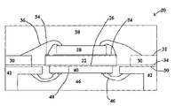
- FIG. 1 a sectional side view of a shielded integrated circuit package indicated generally by the numeral 20 .
- the package 20 includes a die attach pad 22 having a first side 24 and a second side 26 .
- a first semiconductor die 28 is mounted to the first side 24 of the die attach pad 22 .
- a plurality of contact pads 30 are disposed in close proximity to the first semiconductor die 28 and each contact pad 30 has a first side 32 and a second side 34 .
- a first plurality of wire bonds 36 connect the first semiconductor die 28 and ones of the contact pads 30 .
- An overmold 38 encapsulates the first plurality of wire bonds 36 and the first semiconductor die 28 .
- the die attach pad 22 and the contact pads 30 are embedded in the overmold 38 such that the first side 24 of the die attach pad 22 and the first side 32 of each of the contact pads 30 are encapsulated in the overmold 38 .
- a second semiconductor die 40 is mounted to the second side 26 of the die attach pad 22 and a plurality of leads 42 are disposed in close proximity to the second semiconductor die 40 .
- a second plurality of wire bonds 44 connect the second semiconductor die 40 and ones of the leads 42 and an encapsulant 46 encapsulates the second plurality of wire bonds 44 .
- the second semiconductor die 40 and the leads 42 are embedded in the encapsulant 46 such that a first side 48 of the second semiconductor die 40 and a first side 50 of each of the leads 42 are encapsulated in the encapsulant 46 .
- FIG. 2A there is provided an elevation view of a copper (Cu) panel substrate which forms the raw material of the leadframe indicated generally by the numeral 52 .
- the leadframe strip 52 is divided into a plurality of sections, each of which incorporates a plurality of leadframe units in an array (e.g. 5 ⁇ 5 array). Only one such unit is depicted in the elevation view of FIG. 2A , portions of adjacent units being shown by stippled lines.
- an upper and a lower surface of the leadframe strip 52 is coated with a layer of photo-imageable etch resist such as a photo-imageable epoxy.
- the photo resist is spin coated on the leadframe strip.
- the layer of photo-imageable etch resist is imaged with a photo-tool. This is accomplished by exposure of the etch resist to ultraviolet light masked by the photo-tool, as shown in FIG. 2C , and subsequent developing of the etch resist, as shown in FIG. 2D .
- the etch resist is thereby patterned to provide pits on both the upper and the lower surfaces of the leadframe strip, in which the Cu substrate is exposed.
- the leadframe strip 52 is then immersion etched in order to etch both the top and bottom surfaces and, following which, the etch resist is stripped away using conventional means.
- the resulting pattern of die attach pad 22 and contact pads 30 is shown in FIG. 2E .
- the die attach pad 22 has first side 24 and second side 26 .
- each contact pad 30 has first side 32 and second side 34 .
- the leadframe strip 52 is selectively plated with silver (Ag) or nickel and palladium (Ni/Pd) or nickel and gold (Ni/Au) to facilitate wire bonding ( FIG. 2F ).
- the plating covers a peripheral portion of the first side 24 of the die attach pad 22 and the first side 32 of each of the contact pads 30 . It will be appreciated that the peripheral portion of the die attach pad 22 is plated to form a ground ring 54 for ground bond application.
- a singulated semiconductor die 28 is conventionally mounted via epoxy (or other means) on the first side 24 of the die attach pad 22 , and the epoxy is cured. Gold wires 36 are then bonded between the semiconductor die 28 and peripheral contact pads 30 and between the semiconductor die 28 and the ground ring 54 .
- the leadframe 52 is then molded using a modified mold with the bottom cavity being a flat plate, and subsequently cured, as discussed in Applicants' U.S. Pat. No. 6,229,200, the contents of which are incorporated herein by reference.
- the leadframe 52 after the foregoing steps, is shown in FIG. 2G , which includes overmold 38 of cured plastic or epoxy. Clearly the second side 34 of the contact pads 30 and the second side 26 of the die attach pad 22 are exposed.
- an upper and a lower surface of a second leadframe strip 56 is coated with a layer of photo-imageable etch resist such as a photo-imageable epoxy.
- the photo-imageable etch resist is spin coated on the second leadframe strip 56 .
- the layer of photo-imageable etch resist is imaged with a photo-tool. This is accomplished by exposure of the photo-imageable etch resist to ultraviolet light masked by the photo-tool, as shown in FIG. 2I , and subsequent developing of the etch resist, as shown in FIG. 2J .
- the photo-imageable etch resist is thereby patterned to provide pits on both the upper and the lower surfaces of the second leadframe strip 56 , in which the copper substrate is exposed.
- the second leadframe strip 56 is then immersion etched in order to etch both the top and bottom surfaces and the photo-imageable etch resist is then stripped away using conventional means.
- the resulting pattern of leads 42 is shown in FIG. 2K .
- the leads 42 are selectively plated with silver (Ag) or nickel and palladium (Ni/Pd) or nickel and gold (Ni/Au) to facilitate wire bonding ( FIG. 2L ).
- the strip of leads 42 is then attached to the leadframe strip 52 using a conductive adhesive, or other suitable conductive attachment means.
- a conductive adhesive or other suitable conductive attachment means.
- the second side 34 of the contact pads 30 are in electrical contact with a side 50 of the leads 42 as the leads 42 are attached to the contact pads 30 by conductive material.
- a second singulated semiconductor die 40 is conventionally mounted via epoxy (or other means) on the second (exposed) side 26 of the die attach pad 22 , and the epoxy is cured.
- Gold wires 44 are then bonded between the second semiconductor die 40 and the leads 42 .
- a glob-top material is then added to encapsulate the wires 44 between the second semiconductor die 40 and the leads 42 . As shown in FIG. 2N , the glob-top material surrounds the second semiconductor die 40 and the leads 42 such that the second semiconductor die 40 and the leads 42 are embedded in the glob-top.
- Singulation of the individual units from the full leadframe array 52 is then performed either by saw singulation or die punching resulting in the final configuration of FIG. 2O .
- the individual package 20 is isolated.
- the first semiconductor die 28 is a complementary metal oxide semiconductor (CMOS) analog chip and the second semiconductor die is a radio frequency (RF) chip which is effectively shielded by the die attach pad 22 .
- CMOS complementary metal oxide semiconductor
- RF radio frequency
- FIGS. 3A top 3 O show the processing steps for manufacturing a shielded integrated circuit package according to another embodiment of the present invention.
- FIGS. 3A to 3G of the present embodiment are similar to FIGS. 2A to 2G of the above-described embodiment and will not be further described herein.
- FIG. 3H shows a pair of copper strips 58 , 60 , which form a second leadframe strip.
- the first copper strip 58 is coated on a first surface thereof, with solder plating ( FIG. 3I ). The coating is added to enhance lamination and provide a surface for soldering and solder flux is then added to a portion of the first copper strip 58 ( FIG. 3J ).
- the second copper strip 60 is plated with solder plating on both the top and bottom surface ( FIG. 3K ).
- the second copper strip 60 is then laminated to the first copper strip 58 using a proximity placement and thermal solder reflow technique to form the strip of leads 42 ( FIG. 3L ).
- the second copper strip 60 is laminated to the first copper strip 58 by a hot roller thermo-compressive cladding process.
- the strip of leads 42 is then attached to the leadframe strip 52 using a conductive adhesive, or other suitable conductive attachment means.
- a conductive adhesive or other suitable conductive attachment means.
- the second side 34 of the contact pads 30 are in electrical contact with the side 50 of the leads 42 as the leads 42 are attached to the contact pads 30 by conductive material.
- FIG. 3M is similar to FIG. 2M , except that the strip of leads 42 are formed of a pair of laminated copper strips, rather than formed by an etch process.
- FIGS. 3N and 3O are similar to FIGS. 2N and 2O , respectively, and are not further described herein.
- a strip of LPCC packages is assembled, as described above and shown in FIG. 4A and a strip of exposed die packages is assembled as shown in FIG. 4B .
- the strips are aligned and joined by solder reflow technique ( FIG. 4C ).
- the individual units are saw singulated ( FIG. 4D ).
- FIG. 5 is a sectional side view of a shielded integrated circuit package according to yet another embodiment of the present invention.
- the leads 42 and the second semiconductor die 40 are arranged in a flip-chip manner.
- the semiconductor die 40 is attached to the leads 42 , rather than the second side of the die attach pad 22 such that pads of the semiconductor die 40 are electrically connected to the leads 42 .
- wire bonds between the semiconductor die 40 and the 42 are not required in the present embodiment.
- the leadframe strip is not limited to copper as other leadframe strip materials will occur to those skilled in the art.
- other LPCC manufacturing processes are possible. Rather than building a second package on the LPCC package, the second package can be pre-manufactured and the entire package is then mounted to the LPCC package.
- additional semiconductor dice can be added to provide multi-chip packages. Still other embodiments and variations may occur to those of skill in the art. All such embodiments and variations are believed to be within the scope and sphere of the present invention.
Abstract
Description
Claims (7)
Priority Applications (2)
| Application Number | Priority Date | Filing Date | Title |
|---|---|---|---|
| US10/323,658 US7071545B1 (en) | 2002-12-20 | 2002-12-20 | Shielded integrated circuit package |
| US10/885,966 US7381588B1 (en) | 2002-12-20 | 2004-07-08 | Shielded integrated circuit package |
Applications Claiming Priority (1)
| Application Number | Priority Date | Filing Date | Title |
|---|---|---|---|
| US10/323,658 US7071545B1 (en) | 2002-12-20 | 2002-12-20 | Shielded integrated circuit package |
Related Child Applications (1)
| Application Number | Title | Priority Date | Filing Date |
|---|---|---|---|
| US10/885,966 Division US7381588B1 (en) | 2002-12-20 | 2004-07-08 | Shielded integrated circuit package |
Publications (1)
| Publication Number | Publication Date |
|---|---|
| US7071545B1 true US7071545B1 (en) | 2006-07-04 |
Family
ID=36613735
Family Applications (2)
| Application Number | Title | Priority Date | Filing Date |
|---|---|---|---|
| US10/323,658 Expired - Lifetime US7071545B1 (en) | 2002-12-20 | 2002-12-20 | Shielded integrated circuit package |
| US10/885,966 Expired - Lifetime US7381588B1 (en) | 2002-12-20 | 2004-07-08 | Shielded integrated circuit package |
Family Applications After (1)
| Application Number | Title | Priority Date | Filing Date |
|---|---|---|---|
| US10/885,966 Expired - Lifetime US7381588B1 (en) | 2002-12-20 | 2004-07-08 | Shielded integrated circuit package |
Country Status (1)
| Country | Link |
|---|---|
| US (2) | US7071545B1 (en) |
Cited By (43)
| Publication number | Priority date | Publication date | Assignee | Title |
|---|---|---|---|---|
| US20050176380A1 (en) * | 2004-02-05 | 2005-08-11 | Renesas Technology Corp. | Radio frequency circuit module |
| US20050221604A1 (en) * | 2002-09-30 | 2005-10-06 | Jun He | Interconnect structure for an integrated circuit and method of fabrication |
| US20050253225A1 (en) * | 2003-10-02 | 2005-11-17 | Interdigital Technology Corporation | Wireless coupling of semiconductor dies |
| US20060175696A1 (en) * | 2005-02-04 | 2006-08-10 | Stats Chippac Ltd. | Nested integrated circuit package on package system |
| US20060197207A1 (en) * | 2005-02-22 | 2006-09-07 | Stats Chippac Ltd. | Integrated circuit package system with die and package combination |
| WO2008011585A2 (en) * | 2006-07-21 | 2008-01-24 | Analog Devices, Inc. | Package having a plurality of mounting orientations |
| US20090001563A1 (en) * | 2007-06-27 | 2009-01-01 | Henry Descalzo Bathan | Integrated circuit package in package system with adhesiveless package attach |
| WO2010043205A1 (en) * | 2008-10-16 | 2010-04-22 | Osram Opto Semiconductors Gmbh | Electrical terminal lead for a semiconductor component, semiconductor component, and method for producing an electrical terminal lead |
| US20100127363A1 (en) * | 2006-04-28 | 2010-05-27 | Utac Thai Limited | Very extremely thin semiconductor package |
| CN101183677B (en) * | 2007-03-28 | 2010-06-02 | 日月光半导体制造股份有限公司 | Packaging structure and method for manufacturing the packaging structure |
| US7790512B1 (en) | 2007-11-06 | 2010-09-07 | Utac Thai Limited | Molded leadframe substrate semiconductor package |
| US20100311208A1 (en) * | 2008-05-22 | 2010-12-09 | Utac Thai Limited | Method and apparatus for no lead semiconductor package |
| US20100327432A1 (en) * | 2006-09-26 | 2010-12-30 | Utac Thai Limited | Package with heat transfer |
| US20110018111A1 (en) * | 2009-07-23 | 2011-01-27 | Utac Thai Limited | Leadframe feature to minimize flip-chip semiconductor die collapse during flip-chip reflow |
| US20110039371A1 (en) * | 2008-09-04 | 2011-02-17 | Utac Thai Limited | Flip chip cavity package |
| US20110062568A1 (en) * | 2009-09-15 | 2011-03-17 | Manolito Galera | Folded lands and vias for multichip semiconductor packages |
| US20110133319A1 (en) * | 2009-12-04 | 2011-06-09 | Utac Thai Limited | Auxiliary leadframe member for stabilizing the bond wire process |
| US20110147931A1 (en) * | 2006-04-28 | 2011-06-23 | Utac Thai Limited | Lead frame land grid array with routing connector trace under unit |
| US20110198752A1 (en) * | 2006-04-28 | 2011-08-18 | Utac Thai Limited | Lead frame ball grid array with traces under die |
| US8013437B1 (en) | 2006-09-26 | 2011-09-06 | Utac Thai Limited | Package with heat transfer |
| US20110221051A1 (en) * | 2010-03-11 | 2011-09-15 | Utac Thai Limited | Leadframe based multi terminal ic package |
| US20110232693A1 (en) * | 2009-03-12 | 2011-09-29 | Utac Thai Limited | Metallic solderability preservation coating on metal part of semiconductor package to prevent oxide |
| US20130082405A1 (en) * | 2011-09-30 | 2013-04-04 | Jung Hwan CHUN | Semiconductor Package |
| US8460970B1 (en) | 2006-04-28 | 2013-06-11 | Utac Thai Limited | Lead frame ball grid array with traces under die having interlocking features |
| US8461694B1 (en) | 2006-04-28 | 2013-06-11 | Utac Thai Limited | Lead frame ball grid array with traces under die having interlocking features |
| US8871571B2 (en) | 2010-04-02 | 2014-10-28 | Utac Thai Limited | Apparatus for and methods of attaching heat slugs to package tops |
| US8969136B2 (en) | 2011-03-25 | 2015-03-03 | Stats Chippac Ltd. | Integrated circuit packaging system for electromagnetic interference shielding and method of manufacture thereof |
| US9000590B2 (en) | 2012-05-10 | 2015-04-07 | Utac Thai Limited | Protruding terminals with internal routing interconnections semiconductor device |
| US9006034B1 (en) | 2012-06-11 | 2015-04-14 | Utac Thai Limited | Post-mold for semiconductor package having exposed traces |
| US9082607B1 (en) | 2006-12-14 | 2015-07-14 | Utac Thai Limited | Molded leadframe substrate semiconductor package |
| US9355940B1 (en) | 2009-12-04 | 2016-05-31 | Utac Thai Limited | Auxiliary leadframe member for stabilizing the bond wire process |
| CN105826209A (en) * | 2011-06-20 | 2016-08-03 | 乾坤科技股份有限公司 | Package structure and method to fabricate same |
| US9449905B2 (en) | 2012-05-10 | 2016-09-20 | Utac Thai Limited | Plated terminals with routing interconnections semiconductor device |
| US9601419B1 (en) * | 2014-06-06 | 2017-03-21 | Altera Corporation | Stacked leadframe packages |
| US9761435B1 (en) | 2006-12-14 | 2017-09-12 | Utac Thai Limited | Flip chip cavity package |
| US9805955B1 (en) | 2015-11-10 | 2017-10-31 | UTAC Headquarters Pte. Ltd. | Semiconductor package with multiple molding routing layers and a method of manufacturing the same |
| US9899349B2 (en) | 2009-01-29 | 2018-02-20 | Semiconductor Components Industries, Llc | Semiconductor packages and related methods |
| US10163766B2 (en) | 2016-11-21 | 2018-12-25 | Semiconductor Components Industries, Llc | Methods of forming leadless semiconductor packages with plated leadframes and wettable flanks |
| US10199311B2 (en) | 2009-01-29 | 2019-02-05 | Semiconductor Components Industries, Llc | Leadless semiconductor packages, leadframes therefor, and methods of making |
| US10242953B1 (en) | 2015-05-27 | 2019-03-26 | Utac Headquarters PTE. Ltd | Semiconductor package with plated metal shielding and a method thereof |
| US10242934B1 (en) | 2014-05-07 | 2019-03-26 | Utac Headquarters Pte Ltd. | Semiconductor package with full plating on contact side surfaces and methods thereof |
| US10276477B1 (en) | 2016-05-20 | 2019-04-30 | UTAC Headquarters Pte. Ltd. | Semiconductor package with multiple stacked leadframes and a method of manufacturing the same |
| CN110517998A (en) * | 2018-05-21 | 2019-11-29 | 德州仪器公司 | Two sides are in combination with lead frame |
Families Citing this family (7)
| Publication number | Priority date | Publication date | Assignee | Title |
|---|---|---|---|---|
| JP2006509371A (en) * | 2002-12-09 | 2006-03-16 | アドバンスド インターコネクト テクノロジーズ リミテッド | Package with exposed integrated circuit device |
| US8535986B2 (en) * | 2003-01-13 | 2013-09-17 | Infineon Technologies Ag | Method of packaging an integrated circuit using a laser to remove material from a portion of a lead frame |
| US7709935B2 (en) * | 2003-08-26 | 2010-05-04 | Unisem (Mauritius) Holdings Limited | Reversible leadless package and methods of making and using same |
| US20080179722A1 (en) * | 2007-01-31 | 2008-07-31 | Cyntec Co., Ltd. | Electronic package structure |
| US7868471B2 (en) * | 2007-09-13 | 2011-01-11 | Stats Chippac Ltd. | Integrated circuit package-in-package system with leads |
| US8766428B2 (en) * | 2009-12-02 | 2014-07-01 | Stats Chippac Ltd. | Integrated circuit packaging system with flip chip and method of manufacture thereof |
| US20130200503A1 (en) * | 2012-02-08 | 2013-08-08 | Carsem (M) Sdn, Bhd. | Protective layers in semiconductor packaging |
Citations (22)
| Publication number | Priority date | Publication date | Assignee | Title |
|---|---|---|---|---|
| US4677458A (en) | 1983-11-04 | 1987-06-30 | Control Data Corporation | Ceramic IC package attachment apparatus |
| US5557142A (en) | 1991-02-04 | 1996-09-17 | Motorola, Inc. | Shielded semiconductor device package |
| US5637916A (en) | 1996-02-02 | 1997-06-10 | National Semiconductor Corporation | Carrier based IC packaging arrangement |
| US5644167A (en) * | 1996-03-01 | 1997-07-01 | National Semiconductor Corporation | Integrated circuit package assemblies including an electrostatic discharge interposer |
| US5650659A (en) | 1995-08-04 | 1997-07-22 | National Semiconductor Corporation | Semiconductor component package assembly including an integral RF/EMI shield |
| US5679975A (en) | 1995-12-18 | 1997-10-21 | Integrated Device Technology, Inc. | Conductive encapsulating shield for an integrated circuit |
| US6072122A (en) | 1995-05-31 | 2000-06-06 | Nec Corporation | Multi-chip packaging structure having chips sealably mounted on opposing surfaces of substrates |
| US6222265B1 (en) | 1997-03-10 | 2001-04-24 | Micron Technology, Inc. | Method of constructing stacked packages |
| US6229200B1 (en) | 1998-06-10 | 2001-05-08 | Asat Limited | Saw-singulated leadless plastic chip carrier |
| US6281581B1 (en) | 1997-03-12 | 2001-08-28 | International Business Machines Corporation | Substrate structure for improving attachment reliability of semiconductor chips and modules |
| US6303981B1 (en) | 1999-09-01 | 2001-10-16 | Micron Technology, Inc. | Semiconductor package having stacked dice and leadframes and method of fabrication |
| US6377464B1 (en) | 1999-01-29 | 2002-04-23 | Conexant Systems, Inc. | Multiple chip module with integrated RF capabilities |
| US6410981B2 (en) | 1997-10-24 | 2002-06-25 | Nec Corporation | Vented semiconductor device package having separate substrate, strengthening ring and cap structures |
| US6414383B1 (en) | 1999-07-16 | 2002-07-02 | Agere Systems Guardian Corp. | Very low magnetic field integrated circuit |
| US6545365B2 (en) | 2000-04-26 | 2003-04-08 | Mitsubishi Denki Kabushiki Kaisha | Resin-sealed chip stack type semiconductor device |
| US6569712B2 (en) | 2001-10-19 | 2003-05-27 | Via Technologies, Inc. | Structure of a ball-grid array package substrate and processes for producing thereof |
| US6593662B1 (en) | 2000-06-16 | 2003-07-15 | Siliconware Precision Industries Co., Ltd. | Stacked-die package structure |
| US6593647B2 (en) | 2001-06-15 | 2003-07-15 | Oki Electric Industry Co., Ltd. | Semiconductor device |
| US20040063246A1 (en) | 2002-09-17 | 2004-04-01 | Chippac, Inc. | Semiconductor multi-package module having package stacked over die-down flip chip ball grid array package and having wire bond interconnect between stacked packages |
| US6744126B1 (en) | 2002-01-09 | 2004-06-01 | Bridge Semiconductor Corporation | Multichip semiconductor package device |
| US6744121B2 (en) * | 2001-04-19 | 2004-06-01 | Walton Advanced Electronics Ltd | Multi-chip package |
| US6818978B1 (en) * | 2002-11-19 | 2004-11-16 | Asat Ltd. | Ball grid array package with shielding |
Family Cites Families (9)
| Publication number | Priority date | Publication date | Assignee | Title |
|---|---|---|---|---|
| US6933594B2 (en) * | 1998-06-10 | 2005-08-23 | Asat Ltd. | Leadless plastic chip carrier with etch back pad singulation |
| US6545345B1 (en) * | 2001-03-20 | 2003-04-08 | Amkor Technology, Inc. | Mounting for a package containing a chip |
| US6856007B2 (en) * | 2001-08-28 | 2005-02-15 | Tessera, Inc. | High-frequency chip packages |
| JP3973402B2 (en) * | 2001-10-25 | 2007-09-12 | 株式会社日立製作所 | High frequency circuit module |
| US6916682B2 (en) * | 2001-11-08 | 2005-07-12 | Freescale Semiconductor, Inc. | Semiconductor package device for use with multiple integrated circuits in a stacked configuration and method of formation and testing |
| JP2003174111A (en) * | 2001-12-06 | 2003-06-20 | Sanyo Electric Co Ltd | Semiconductor device |
| US6940154B2 (en) * | 2002-06-24 | 2005-09-06 | Asat Limited | Integrated circuit package and method of manufacturing the integrated circuit package |
| US6933597B1 (en) * | 2002-07-09 | 2005-08-23 | National Semiconductor Corporation | Spacer with passive components for use in multi-chip modules |
| US7064426B2 (en) * | 2002-09-17 | 2006-06-20 | Chippac, Inc. | Semiconductor multi-package module having wire bond interconnect between stacked packages |
-
2002
- 2002-12-20 US US10/323,658 patent/US7071545B1/en not_active Expired - Lifetime
-
2004
- 2004-07-08 US US10/885,966 patent/US7381588B1/en not_active Expired - Lifetime
Patent Citations (22)
| Publication number | Priority date | Publication date | Assignee | Title |
|---|---|---|---|---|
| US4677458A (en) | 1983-11-04 | 1987-06-30 | Control Data Corporation | Ceramic IC package attachment apparatus |
| US5557142A (en) | 1991-02-04 | 1996-09-17 | Motorola, Inc. | Shielded semiconductor device package |
| US6072122A (en) | 1995-05-31 | 2000-06-06 | Nec Corporation | Multi-chip packaging structure having chips sealably mounted on opposing surfaces of substrates |
| US5650659A (en) | 1995-08-04 | 1997-07-22 | National Semiconductor Corporation | Semiconductor component package assembly including an integral RF/EMI shield |
| US5679975A (en) | 1995-12-18 | 1997-10-21 | Integrated Device Technology, Inc. | Conductive encapsulating shield for an integrated circuit |
| US5637916A (en) | 1996-02-02 | 1997-06-10 | National Semiconductor Corporation | Carrier based IC packaging arrangement |
| US5644167A (en) * | 1996-03-01 | 1997-07-01 | National Semiconductor Corporation | Integrated circuit package assemblies including an electrostatic discharge interposer |
| US6222265B1 (en) | 1997-03-10 | 2001-04-24 | Micron Technology, Inc. | Method of constructing stacked packages |
| US6281581B1 (en) | 1997-03-12 | 2001-08-28 | International Business Machines Corporation | Substrate structure for improving attachment reliability of semiconductor chips and modules |
| US6410981B2 (en) | 1997-10-24 | 2002-06-25 | Nec Corporation | Vented semiconductor device package having separate substrate, strengthening ring and cap structures |
| US6229200B1 (en) | 1998-06-10 | 2001-05-08 | Asat Limited | Saw-singulated leadless plastic chip carrier |
| US6377464B1 (en) | 1999-01-29 | 2002-04-23 | Conexant Systems, Inc. | Multiple chip module with integrated RF capabilities |
| US6414383B1 (en) | 1999-07-16 | 2002-07-02 | Agere Systems Guardian Corp. | Very low magnetic field integrated circuit |
| US6303981B1 (en) | 1999-09-01 | 2001-10-16 | Micron Technology, Inc. | Semiconductor package having stacked dice and leadframes and method of fabrication |
| US6545365B2 (en) | 2000-04-26 | 2003-04-08 | Mitsubishi Denki Kabushiki Kaisha | Resin-sealed chip stack type semiconductor device |
| US6593662B1 (en) | 2000-06-16 | 2003-07-15 | Siliconware Precision Industries Co., Ltd. | Stacked-die package structure |
| US6744121B2 (en) * | 2001-04-19 | 2004-06-01 | Walton Advanced Electronics Ltd | Multi-chip package |
| US6593647B2 (en) | 2001-06-15 | 2003-07-15 | Oki Electric Industry Co., Ltd. | Semiconductor device |
| US6569712B2 (en) | 2001-10-19 | 2003-05-27 | Via Technologies, Inc. | Structure of a ball-grid array package substrate and processes for producing thereof |
| US6744126B1 (en) | 2002-01-09 | 2004-06-01 | Bridge Semiconductor Corporation | Multichip semiconductor package device |
| US20040063246A1 (en) | 2002-09-17 | 2004-04-01 | Chippac, Inc. | Semiconductor multi-package module having package stacked over die-down flip chip ball grid array package and having wire bond interconnect between stacked packages |
| US6818978B1 (en) * | 2002-11-19 | 2004-11-16 | Asat Ltd. | Ball grid array package with shielding |
Cited By (105)
| Publication number | Priority date | Publication date | Assignee | Title |
|---|---|---|---|---|
| US20050221604A1 (en) * | 2002-09-30 | 2005-10-06 | Jun He | Interconnect structure for an integrated circuit and method of fabrication |
| US7151051B2 (en) * | 2002-09-30 | 2006-12-19 | Intel Corporation | Interconnect structure for an integrated circuit and method of fabrication |
| US7304374B2 (en) * | 2003-10-02 | 2007-12-04 | Interdigital Technology Corporation | Wireless coupling of semiconductor dies |
| US20050253225A1 (en) * | 2003-10-02 | 2005-11-17 | Interdigital Technology Corporation | Wireless coupling of semiconductor dies |
| US7515879B2 (en) * | 2004-02-05 | 2009-04-07 | Renesas Technology Corp. | Radio frequency circuit module |
| US20050176380A1 (en) * | 2004-02-05 | 2005-08-11 | Renesas Technology Corp. | Radio frequency circuit module |
| US7279786B2 (en) * | 2005-02-04 | 2007-10-09 | Stats Chippac Ltd. | Nested integrated circuit package on package system |
| US20070290319A1 (en) * | 2005-02-04 | 2007-12-20 | Hyun Uk Kim | Nested integrated circuit package on package system |
| US8169064B2 (en) * | 2005-02-04 | 2012-05-01 | Stats Chippac Ltd. | Nested integrated circuit package on package system |
| US20060175696A1 (en) * | 2005-02-04 | 2006-08-10 | Stats Chippac Ltd. | Nested integrated circuit package on package system |
| US7598606B2 (en) * | 2005-02-22 | 2009-10-06 | Stats Chippac Ltd. | Integrated circuit package system with die and package combination |
| US8102040B2 (en) | 2005-02-22 | 2012-01-24 | Stats Chippac Ltd. | Integrated circuit package system with die and package combination |
| US20090309207A1 (en) * | 2005-02-22 | 2009-12-17 | Seng Guan Chow | Integrated circuit package system with die and package combination |
| US20060197207A1 (en) * | 2005-02-22 | 2006-09-07 | Stats Chippac Ltd. | Integrated circuit package system with die and package combination |
| US8652879B2 (en) | 2006-04-28 | 2014-02-18 | Utac Thai Limited | Lead frame ball grid array with traces under die |
| US8685794B2 (en) | 2006-04-28 | 2014-04-01 | Utac Thai Limited | Lead frame land grid array with routing connector trace under unit |
| US8575762B2 (en) | 2006-04-28 | 2013-11-05 | Utac Thai Limited | Very extremely thin semiconductor package |
| US20100127363A1 (en) * | 2006-04-28 | 2010-05-27 | Utac Thai Limited | Very extremely thin semiconductor package |
| US8492906B2 (en) | 2006-04-28 | 2013-07-23 | Utac Thai Limited | Lead frame ball grid array with traces under die |
| US8487451B2 (en) | 2006-04-28 | 2013-07-16 | Utac Thai Limited | Lead frame land grid array with routing connector trace under unit |
| US8461694B1 (en) | 2006-04-28 | 2013-06-11 | Utac Thai Limited | Lead frame ball grid array with traces under die having interlocking features |
| US8460970B1 (en) | 2006-04-28 | 2013-06-11 | Utac Thai Limited | Lead frame ball grid array with traces under die having interlocking features |
| US8310060B1 (en) | 2006-04-28 | 2012-11-13 | Utac Thai Limited | Lead frame land grid array |
| US8704381B2 (en) | 2006-04-28 | 2014-04-22 | Utac Thai Limited | Very extremely thin semiconductor package |
| US9099317B2 (en) | 2006-04-28 | 2015-08-04 | Utac Thai Limited | Method for forming lead frame land grid array |
| US20110198752A1 (en) * | 2006-04-28 | 2011-08-18 | Utac Thai Limited | Lead frame ball grid array with traces under die |
| US20110147931A1 (en) * | 2006-04-28 | 2011-06-23 | Utac Thai Limited | Lead frame land grid array with routing connector trace under unit |
| US7968807B2 (en) * | 2006-07-21 | 2011-06-28 | Analog Devices, Inc. | Package having a plurality of mounting orientations |
| WO2008011585A2 (en) * | 2006-07-21 | 2008-01-24 | Analog Devices, Inc. | Package having a plurality of mounting orientations |
| US20080205025A1 (en) * | 2006-07-21 | 2008-08-28 | Analog Devices, Inc. | Package Having a Plurality of Mounting Orientations |
| WO2008011585A3 (en) * | 2006-07-21 | 2008-03-06 | Analog Devices Inc | Package having a plurality of mounting orientations |
| US8125077B2 (en) | 2006-09-26 | 2012-02-28 | Utac Thai Limited | Package with heat transfer |
| US20100327432A1 (en) * | 2006-09-26 | 2010-12-30 | Utac Thai Limited | Package with heat transfer |
| US8013437B1 (en) | 2006-09-26 | 2011-09-06 | Utac Thai Limited | Package with heat transfer |
| US9711343B1 (en) | 2006-12-14 | 2017-07-18 | Utac Thai Limited | Molded leadframe substrate semiconductor package |
| US9196470B1 (en) | 2006-12-14 | 2015-11-24 | Utac Thai Limited | Molded leadframe substrate semiconductor package |
| US9099294B1 (en) | 2006-12-14 | 2015-08-04 | Utac Thai Limited | Molded leadframe substrate semiconductor package |
| US9761435B1 (en) | 2006-12-14 | 2017-09-12 | Utac Thai Limited | Flip chip cavity package |
| US9093486B2 (en) | 2006-12-14 | 2015-07-28 | Utac Thai Limited | Molded leadframe substrate semiconductor package |
| US9082607B1 (en) | 2006-12-14 | 2015-07-14 | Utac Thai Limited | Molded leadframe substrate semiconductor package |
| US9899208B2 (en) | 2006-12-14 | 2018-02-20 | Utac Thai Limited | Molded leadframe substrate semiconductor package |
| CN101183677B (en) * | 2007-03-28 | 2010-06-02 | 日月光半导体制造股份有限公司 | Packaging structure and method for manufacturing the packaging structure |
| US8203214B2 (en) * | 2007-06-27 | 2012-06-19 | Stats Chippac Ltd. | Integrated circuit package in package system with adhesiveless package attach |
| US20090001563A1 (en) * | 2007-06-27 | 2009-01-01 | Henry Descalzo Bathan | Integrated circuit package in package system with adhesiveless package attach |
| US7790512B1 (en) | 2007-11-06 | 2010-09-07 | Utac Thai Limited | Molded leadframe substrate semiconductor package |
| US8338922B1 (en) | 2007-11-06 | 2012-12-25 | Utac Thai Limited | Molded leadframe substrate semiconductor package |
| US20100311208A1 (en) * | 2008-05-22 | 2010-12-09 | Utac Thai Limited | Method and apparatus for no lead semiconductor package |
| US8071426B2 (en) | 2008-05-22 | 2011-12-06 | Utac Thai Limited | Method and apparatus for no lead semiconductor package |
| US8063470B1 (en) | 2008-05-22 | 2011-11-22 | Utac Thai Limited | Method and apparatus for no lead semiconductor package |
| US9947605B2 (en) | 2008-09-04 | 2018-04-17 | UTAC Headquarters Pte. Ltd. | Flip chip cavity package |
| US20110039371A1 (en) * | 2008-09-04 | 2011-02-17 | Utac Thai Limited | Flip chip cavity package |
| TWI404186B (en) * | 2008-10-16 | 2013-08-01 | Osram Opto Semiconductors Gmbh | Electric connection conductor for a semiconductor component, semiconductor component and method for the production of an electric connection conductor |
| WO2010043205A1 (en) * | 2008-10-16 | 2010-04-22 | Osram Opto Semiconductors Gmbh | Electrical terminal lead for a semiconductor component, semiconductor component, and method for producing an electrical terminal lead |
| US10756006B2 (en) | 2009-01-29 | 2020-08-25 | Semiconductor Components Industries, Llc | Leadless semiconductor packages, leadframes therefor, and methods of making |
| US10304798B2 (en) | 2009-01-29 | 2019-05-28 | Semiconductor Components Industries, Llc | Semiconductor packages with leadframes and related methods |
| US11049843B2 (en) | 2009-01-29 | 2021-06-29 | Semiconductor Components Industries, Llc | Semiconductor packages |
| US9899349B2 (en) | 2009-01-29 | 2018-02-20 | Semiconductor Components Industries, Llc | Semiconductor packages and related methods |
| US10199311B2 (en) | 2009-01-29 | 2019-02-05 | Semiconductor Components Industries, Llc | Leadless semiconductor packages, leadframes therefor, and methods of making |
| US20110232693A1 (en) * | 2009-03-12 | 2011-09-29 | Utac Thai Limited | Metallic solderability preservation coating on metal part of semiconductor package to prevent oxide |
| US8367476B2 (en) | 2009-03-12 | 2013-02-05 | Utac Thai Limited | Metallic solderability preservation coating on metal part of semiconductor package to prevent oxide |
| US8569877B2 (en) | 2009-03-12 | 2013-10-29 | Utac Thai Limited | Metallic solderability preservation coating on metal part of semiconductor package to prevent oxide |
| US8431443B2 (en) | 2009-03-12 | 2013-04-30 | Utac Thai Limited | Metallic solderability preservation coating on metal part of semiconductor package to prevent oxide |
| US20110018111A1 (en) * | 2009-07-23 | 2011-01-27 | Utac Thai Limited | Leadframe feature to minimize flip-chip semiconductor die collapse during flip-chip reflow |
| US9449900B2 (en) | 2009-07-23 | 2016-09-20 | UTAC Headquarters Pte. Ltd. | Leadframe feature to minimize flip-chip semiconductor die collapse during flip-chip reflow |
| US8072051B2 (en) * | 2009-09-15 | 2011-12-06 | Fairchild Semiconductor Corporation | Folded lands and vias for multichip semiconductor packages |
| US20110062568A1 (en) * | 2009-09-15 | 2011-03-17 | Manolito Galera | Folded lands and vias for multichip semiconductor packages |
| US9355940B1 (en) | 2009-12-04 | 2016-05-31 | Utac Thai Limited | Auxiliary leadframe member for stabilizing the bond wire process |
| US20110133319A1 (en) * | 2009-12-04 | 2011-06-09 | Utac Thai Limited | Auxiliary leadframe member for stabilizing the bond wire process |
| US8368189B2 (en) | 2009-12-04 | 2013-02-05 | Utac Thai Limited | Auxiliary leadframe member for stabilizing the bond wire process |
| US8575732B2 (en) | 2010-03-11 | 2013-11-05 | Utac Thai Limited | Leadframe based multi terminal IC package |
| US8722461B2 (en) | 2010-03-11 | 2014-05-13 | Utac Thai Limited | Leadframe based multi terminal IC package |
| US20110221051A1 (en) * | 2010-03-11 | 2011-09-15 | Utac Thai Limited | Leadframe based multi terminal ic package |
| US8871571B2 (en) | 2010-04-02 | 2014-10-28 | Utac Thai Limited | Apparatus for and methods of attaching heat slugs to package tops |
| US8969136B2 (en) | 2011-03-25 | 2015-03-03 | Stats Chippac Ltd. | Integrated circuit packaging system for electromagnetic interference shielding and method of manufacture thereof |
| CN105826209A (en) * | 2011-06-20 | 2016-08-03 | 乾坤科技股份有限公司 | Package structure and method to fabricate same |
| US20200176270A1 (en) * | 2011-06-20 | 2020-06-04 | Cyntec Co., Ltd. | A Stack Frame for Electrical Connections and the Method to Fabricate Thereof |
| US11031255B2 (en) * | 2011-06-20 | 2021-06-08 | Cyntec Co., Ltd. | Stack frame for electrical connections and the method to fabricate thereof |
| US9514964B2 (en) * | 2011-06-20 | 2016-12-06 | Cyntec Co., Ltd. | Stack frame for electrical connections and the method to fabricate thereof |
| CN105826209B (en) * | 2011-06-20 | 2021-07-13 | 乾坤科技股份有限公司 | Packaging structure and manufacturing method thereof |
| US8952514B2 (en) * | 2011-09-30 | 2015-02-10 | Sts Semiconductor & Telecommunications Co., Ltd. | Semiconductor package |
| US20130082405A1 (en) * | 2011-09-30 | 2013-04-04 | Jung Hwan CHUN | Semiconductor Package |
| US9000590B2 (en) | 2012-05-10 | 2015-04-07 | Utac Thai Limited | Protruding terminals with internal routing interconnections semiconductor device |
| US9922914B2 (en) | 2012-05-10 | 2018-03-20 | Utac Thai Limited | Plated terminals with routing interconnections semiconductor device |
| US9972563B2 (en) | 2012-05-10 | 2018-05-15 | UTAC Headquarters Pte. Ltd. | Plated terminals with routing interconnections semiconductor device |
| US9029198B2 (en) | 2012-05-10 | 2015-05-12 | Utac Thai Limited | Methods of manufacturing semiconductor devices including terminals with internal routing interconnections |
| US9922913B2 (en) | 2012-05-10 | 2018-03-20 | Utac Thai Limited | Plated terminals with routing interconnections semiconductor device |
| US9449905B2 (en) | 2012-05-10 | 2016-09-20 | Utac Thai Limited | Plated terminals with routing interconnections semiconductor device |
| US9006034B1 (en) | 2012-06-11 | 2015-04-14 | Utac Thai Limited | Post-mold for semiconductor package having exposed traces |
| US9397031B2 (en) | 2012-06-11 | 2016-07-19 | Utac Thai Limited | Post-mold for semiconductor package having exposed traces |
| US10242934B1 (en) | 2014-05-07 | 2019-03-26 | Utac Headquarters Pte Ltd. | Semiconductor package with full plating on contact side surfaces and methods thereof |
| US9601419B1 (en) * | 2014-06-06 | 2017-03-21 | Altera Corporation | Stacked leadframe packages |
| US10269686B1 (en) | 2015-05-27 | 2019-04-23 | UTAC Headquarters PTE, LTD. | Method of improving adhesion between molding compounds and an apparatus thereof |
| US10242953B1 (en) | 2015-05-27 | 2019-03-26 | Utac Headquarters PTE. Ltd | Semiconductor package with plated metal shielding and a method thereof |
| US10096490B2 (en) | 2015-11-10 | 2018-10-09 | UTAC Headquarters Pte. Ltd. | Semiconductor package with multiple molding routing layers and a method of manufacturing the same |
| US9805955B1 (en) | 2015-11-10 | 2017-10-31 | UTAC Headquarters Pte. Ltd. | Semiconductor package with multiple molding routing layers and a method of manufacturing the same |
| US10325782B2 (en) | 2015-11-10 | 2019-06-18 | UTAC Headquarters Pte. Ltd. | Semiconductor package with multiple molding routing layers and a method of manufacturing the same |
| US9917038B1 (en) | 2015-11-10 | 2018-03-13 | Utac Headquarters Pte Ltd | Semiconductor package with multiple molding routing layers and a method of manufacturing the same |
| US10734247B2 (en) | 2015-11-10 | 2020-08-04 | Utac Headquarters PTE. Ltd | Semiconductor package with multiple molding routing layers and a method of manufacturing the same |
| US10163658B2 (en) | 2015-11-10 | 2018-12-25 | UTAC Headquarters PTE, LTD. | Semiconductor package with multiple molding routing layers and a method of manufacturing the same |
| US10032645B1 (en) | 2015-11-10 | 2018-07-24 | UTAC Headquarters Pte. Ltd. | Semiconductor package with multiple molding routing layers and a method of manufacturing the same |
| US9922843B1 (en) | 2015-11-10 | 2018-03-20 | UTAC Headquarters Pte. Ltd. | Semiconductor package with multiple molding routing layers and a method of manufacturing the same |
| US10276477B1 (en) | 2016-05-20 | 2019-04-30 | UTAC Headquarters Pte. Ltd. | Semiconductor package with multiple stacked leadframes and a method of manufacturing the same |
| US10163766B2 (en) | 2016-11-21 | 2018-12-25 | Semiconductor Components Industries, Llc | Methods of forming leadless semiconductor packages with plated leadframes and wettable flanks |
| US11145581B2 (en) | 2016-11-21 | 2021-10-12 | Semiconductor Components Industries, Llc | Methods of forming leadless semiconductor packages with plated leadframes and wettable flanks |
| CN110517998A (en) * | 2018-05-21 | 2019-11-29 | 德州仪器公司 | Two sides are in combination with lead frame |
Also Published As
| Publication number | Publication date |
|---|---|
| US7381588B1 (en) | 2008-06-03 |
Similar Documents
| Publication | Publication Date | Title |
|---|---|---|
| US7071545B1 (en) | Shielded integrated circuit package | |
| US11289409B2 (en) | Method for fabricating carrier-free semiconductor package | |
| US6818978B1 (en) | Ball grid array package with shielding | |
| US7009286B1 (en) | Thin leadless plastic chip carrier | |
| US6585905B1 (en) | Leadless plastic chip carrier with partial etch die attach pad | |
| US7411289B1 (en) | Integrated circuit package with partially exposed contact pads and process for fabricating the same | |
| US6459163B1 (en) | Semiconductor device and method for fabricating the same | |
| US7247526B1 (en) | Process for fabricating an integrated circuit package | |
| US6586834B1 (en) | Die-up tape ball grid array package | |
| US7259445B2 (en) | Thermal enhanced package for block mold assembly | |
| US6964918B1 (en) | Electronic components such as thin array plastic packages and process for fabricating same | |
| US7358119B2 (en) | Thin array plastic package without die attach pad and process for fabricating the same | |
| US7482690B1 (en) | Electronic components such as thin array plastic packages and process for fabricating same | |
| US5953589A (en) | Ball grid array semiconductor package with solder balls fused on printed circuit board and method for fabricating the same | |
| US5467253A (en) | Semiconductor chip package and method of forming | |
| US7226811B1 (en) | Process for fabricating a leadless plastic chip carrier | |
| US7049177B1 (en) | Leadless plastic chip carrier with standoff contacts and die attach pad | |
| US7348663B1 (en) | Integrated circuit package and method for fabricating same | |
| US7595225B1 (en) | Leadless plastic chip carrier with contact standoff | |
| US9520306B2 (en) | Method of fabricating an integrated circuit (IC) package having a plurality of spaced apart pad portion | |
| US20050218499A1 (en) | Method for manufacturing leadless semiconductor packages | |
| US20070065984A1 (en) | Thermal enhanced package for block mold assembly | |
| US7410830B1 (en) | Leadless plastic chip carrier and method of fabricating same | |
| US6876087B2 (en) | Chip scale package with heat dissipating part | |
| US10658277B2 (en) | Semiconductor package with a heat spreader and method of manufacturing thereof |
Legal Events
| Date | Code | Title | Description |
|---|---|---|---|
| AS | Assignment |
Owner name: ASAT LTD., HONG KONG Free format text: ASSIGNMENT OF ASSIGNORS INTEREST;ASSIGNORS:PATEL, VIRESH;KIRLOSKAR, MOHAN;REEL/FRAME:014025/0871;SIGNING DATES FROM 20030304 TO 20030305 |
|
| STCF | Information on status: patent grant |
Free format text: PATENTED CASE |
|
| FEPP | Fee payment procedure |
Free format text: PAYER NUMBER DE-ASSIGNED (ORIGINAL EVENT CODE: RMPN); ENTITY STATUS OF PATENT OWNER: LARGE ENTITY Free format text: PAYOR NUMBER ASSIGNED (ORIGINAL EVENT CODE: ASPN); ENTITY STATUS OF PATENT OWNER: LARGE ENTITY |
|
| FPAY | Fee payment |
Year of fee payment: 4 |
|
| AS | Assignment |
Owner name: JPMORGAN CHASE BANK, N.A., AS COLLATERAL AGENT,TEX Free format text: GRANT OF SECURITY INTEREST IN PATENT RIGHTS - FIRST PRIORITY;ASSIGNOR:UTAC HONG KONG LIMITED;REEL/FRAME:024599/0743 Effective date: 20100604 Owner name: JPMORGAN CHASE BANK, N.A., AS COLLATERAL AGENT,TEX Free format text: GRANT OF SECURITY INTEREST IN PATENT RIGHTS - SECOND PRIORITY;ASSIGNOR:UTAC HONG KONG LIMITED;REEL/FRAME:024599/0827 Effective date: 20100604 Owner name: THE HONGKONG AND SHANGHAI BANKING CORPORATION LIMI Free format text: GRANT OF SECURITY INTEREST IN PATENT RIGHTS - SECOND PRIORITY;ASSIGNOR:UTAC HONG KONG LIMITED;REEL/FRAME:024611/0097 Effective date: 20100604 Owner name: JPMORGAN CHASE BANK, N.A., AS COLLATERAL AGENT, TE Free format text: GRANT OF SECURITY INTEREST IN PATENT RIGHTS - FIRST PRIORITY;ASSIGNOR:UTAC HONG KONG LIMITED;REEL/FRAME:024599/0743 Effective date: 20100604 Owner name: JPMORGAN CHASE BANK, N.A., AS COLLATERAL AGENT, TE Free format text: GRANT OF SECURITY INTEREST IN PATENT RIGHTS - SECOND PRIORITY;ASSIGNOR:UTAC HONG KONG LIMITED;REEL/FRAME:024599/0827 Effective date: 20100604 |
|
| AS | Assignment |
Owner name: UTAC HONG KONG LIMITED, HONG KONG Free format text: CHANGE OF NAME;ASSIGNOR:ASAT LIMITED;REEL/FRAME:025217/0366 Effective date: 20100325 |
|
| FPAY | Fee payment |
Year of fee payment: 8 |
|
| AS | Assignment |
Owner name: UTAC HEADQUARTERS PTE. LTD., SINGAPORE Free format text: ASSIGNMENT OF ASSIGNORS INTEREST;ASSIGNOR:UTAC HONG KONG LIMITED;REEL/FRAME:037880/0534 Effective date: 20150508 |
|
| AS | Assignment |
Owner name: UTAC HEADQUARTERS PTE. LTD., SINGAPORE Free format text: CORRECTIVE ASSIGNMENT TO CORRECT THE ADD ANNEX INADVERTENTLY LEFT OUT ORIGINAL ASSIGNMENT DOCUMENT PREVIOUSLY RECORDED AT REEL: 037880 FRAME: 0534. ASSIGNOR(S) HEREBY CONFIRMS THE ASSIGNMENT;ASSIGNOR:UTAC HONG KONG LIMITED;REEL/FRAME:039822/0591 Effective date: 20150508 |
|
| MAFP | Maintenance fee payment |
Free format text: PAYMENT OF MAINTENANCE FEE, 12TH YEAR, LARGE ENTITY (ORIGINAL EVENT CODE: M1553) Year of fee payment: 12 |