US7115811B2 - Semiconductor body forming a solar cell with a bypass diode - Google Patents
Semiconductor body forming a solar cell with a bypass diode Download PDFInfo
- Publication number
- US7115811B2 US7115811B2 US10/336,247 US33624703A US7115811B2 US 7115811 B2 US7115811 B2 US 7115811B2 US 33624703 A US33624703 A US 33624703A US 7115811 B2 US7115811 B2 US 7115811B2
- Authority
- US
- United States
- Prior art keywords
- solar cell
- layers
- sequence
- bypass diode
- region
- Prior art date
- Legal status (The legal status is an assumption and is not a legal conclusion. Google has not performed a legal analysis and makes no representation as to the accuracy of the status listed.)
- Expired - Lifetime, expires
Links
- 239000004065 semiconductor Substances 0.000 title claims description 18
- 229910052751 metal Inorganic materials 0.000 claims description 29
- 239000002184 metal Substances 0.000 claims description 29
- 239000000758 substrate Substances 0.000 claims description 25
- 229910001218 Gallium arsenide Inorganic materials 0.000 claims description 24
- 239000000463 material Substances 0.000 claims description 18
- 230000002441 reversible effect Effects 0.000 claims description 16
- 229910052732 germanium Inorganic materials 0.000 claims description 9
- GNPVGFCGXDBREM-UHFFFAOYSA-N germanium atom Chemical compound [Ge] GNPVGFCGXDBREM-UHFFFAOYSA-N 0.000 claims description 9
- 239000012212 insulator Substances 0.000 claims description 8
- 239000000203 mixture Substances 0.000 claims description 4
- 239000002674 ointment Substances 0.000 claims 1
- 238000000034 method Methods 0.000 abstract description 29
- 229920002120 photoresistant polymer Polymers 0.000 description 14
- 238000012545 processing Methods 0.000 description 13
- 239000006059 cover glass Substances 0.000 description 8
- CSCPPACGZOOCGX-UHFFFAOYSA-N Acetone Chemical compound CC(C)=O CSCPPACGZOOCGX-UHFFFAOYSA-N 0.000 description 6
- 230000001681 protective effect Effects 0.000 description 5
- 229910000980 Aluminium gallium arsenide Inorganic materials 0.000 description 4
- 230000008901 benefit Effects 0.000 description 4
- 238000007796 conventional method Methods 0.000 description 4
- 230000015556 catabolic process Effects 0.000 description 3
- KRKNYBCHXYNGOX-UHFFFAOYSA-N citric acid Chemical compound OC(=O)CC(O)(C(O)=O)CC(O)=O KRKNYBCHXYNGOX-UHFFFAOYSA-N 0.000 description 3
- 230000000295 complement effect Effects 0.000 description 3
- 238000004519 manufacturing process Methods 0.000 description 3
- 150000002739 metals Chemical class 0.000 description 3
- 230000008569 process Effects 0.000 description 3
- 230000005855 radiation Effects 0.000 description 3
- 238000012360 testing method Methods 0.000 description 3
- 229910000530 Gallium indium arsenide Inorganic materials 0.000 description 2
- 239000006117 anti-reflective coating Substances 0.000 description 2
- 150000001875 compounds Chemical class 0.000 description 2
- 239000013078 crystal Substances 0.000 description 2
- 238000000151 deposition Methods 0.000 description 2
- 230000008021 deposition Effects 0.000 description 2
- 239000002019 doping agent Substances 0.000 description 2
- 230000005611 electricity Effects 0.000 description 2
- 238000005530 etching Methods 0.000 description 2
- 238000005259 measurement Methods 0.000 description 2
- 238000001741 metal-organic molecular beam epitaxy Methods 0.000 description 2
- 229910052594 sapphire Inorganic materials 0.000 description 2
- 239000010980 sapphire Substances 0.000 description 2
- 238000001228 spectrum Methods 0.000 description 2
- 229910017401 Au—Ge Inorganic materials 0.000 description 1
- 229910001374 Invar Inorganic materials 0.000 description 1
- ZOKXTWBITQBERF-UHFFFAOYSA-N Molybdenum Chemical compound [Mo] ZOKXTWBITQBERF-UHFFFAOYSA-N 0.000 description 1
- 239000002253 acid Substances 0.000 description 1
- 239000000853 adhesive Substances 0.000 description 1
- 230000001070 adhesive effect Effects 0.000 description 1
- 229910045601 alloy Inorganic materials 0.000 description 1
- 239000000956 alloy Substances 0.000 description 1
- 230000003667 anti-reflective effect Effects 0.000 description 1
- 238000013459 approach Methods 0.000 description 1
- 238000003491 array Methods 0.000 description 1
- 230000000712 assembly Effects 0.000 description 1
- 238000000429 assembly Methods 0.000 description 1
- 230000015572 biosynthetic process Effects 0.000 description 1
- 230000008859 change Effects 0.000 description 1
- 238000005229 chemical vapour deposition Methods 0.000 description 1
- 239000011248 coating agent Substances 0.000 description 1
- 238000000576 coating method Methods 0.000 description 1
- 239000004020 conductor Substances 0.000 description 1
- 230000008878 coupling Effects 0.000 description 1
- 238000010168 coupling process Methods 0.000 description 1
- 238000005859 coupling reaction Methods 0.000 description 1
- 230000001351 cycling effect Effects 0.000 description 1
- 238000006731 degradation reaction Methods 0.000 description 1
- 238000013461 design Methods 0.000 description 1
- 238000009792 diffusion process Methods 0.000 description 1
- 230000002900 effect on cell Effects 0.000 description 1
- 238000005516 engineering process Methods 0.000 description 1
- 238000000407 epitaxy Methods 0.000 description 1
- 230000005496 eutectics Effects 0.000 description 1
- 239000002803 fossil fuel Substances 0.000 description 1
- 230000017525 heat dissipation Effects 0.000 description 1
- 238000005286 illumination Methods 0.000 description 1
- 239000012535 impurity Substances 0.000 description 1
- 239000007788 liquid Substances 0.000 description 1
- 230000007246 mechanism Effects 0.000 description 1
- 238000001883 metal evaporation Methods 0.000 description 1
- 229910052750 molybdenum Inorganic materials 0.000 description 1
- 239000011733 molybdenum Substances 0.000 description 1
- 230000003287 optical effect Effects 0.000 description 1
- 238000012856 packing Methods 0.000 description 1
- 239000002245 particle Substances 0.000 description 1
- 230000006798 recombination Effects 0.000 description 1
- 238000005215 recombination Methods 0.000 description 1
- 229910052709 silver Inorganic materials 0.000 description 1
- 239000004332 silver Substances 0.000 description 1
- 238000005476 soldering Methods 0.000 description 1
- 230000002459 sustained effect Effects 0.000 description 1
- 238000000927 vapour-phase epitaxy Methods 0.000 description 1
Images


Classifications
-
- H—ELECTRICITY
- H01—ELECTRIC ELEMENTS
- H01L—SEMICONDUCTOR DEVICES NOT COVERED BY CLASS H10
- H01L31/00—Semiconductor devices sensitive to infrared radiation, light, electromagnetic radiation of shorter wavelength or corpuscular radiation and specially adapted either for the conversion of the energy of such radiation into electrical energy or for the control of electrical energy by such radiation; Processes or apparatus specially adapted for the manufacture or treatment thereof or of parts thereof; Details thereof
- H01L31/04—Semiconductor devices sensitive to infrared radiation, light, electromagnetic radiation of shorter wavelength or corpuscular radiation and specially adapted either for the conversion of the energy of such radiation into electrical energy or for the control of electrical energy by such radiation; Processes or apparatus specially adapted for the manufacture or treatment thereof or of parts thereof; Details thereof adapted as photovoltaic [PV] conversion devices
- H01L31/06—Semiconductor devices sensitive to infrared radiation, light, electromagnetic radiation of shorter wavelength or corpuscular radiation and specially adapted either for the conversion of the energy of such radiation into electrical energy or for the control of electrical energy by such radiation; Processes or apparatus specially adapted for the manufacture or treatment thereof or of parts thereof; Details thereof adapted as photovoltaic [PV] conversion devices characterised by at least one potential-jump barrier or surface barrier
- H01L31/068—Semiconductor devices sensitive to infrared radiation, light, electromagnetic radiation of shorter wavelength or corpuscular radiation and specially adapted either for the conversion of the energy of such radiation into electrical energy or for the control of electrical energy by such radiation; Processes or apparatus specially adapted for the manufacture or treatment thereof or of parts thereof; Details thereof adapted as photovoltaic [PV] conversion devices characterised by at least one potential-jump barrier or surface barrier the potential barriers being only of the PN homojunction type, e.g. bulk silicon PN homojunction solar cells or thin film polycrystalline silicon PN homojunction solar cells
- H01L31/0687—Multiple junction or tandem solar cells
- H01L31/06875—Multiple junction or tandem solar cells inverted grown metamorphic [IMM] multiple junction solar cells, e.g. III-V compounds inverted metamorphic multi-junction cells
-
- H—ELECTRICITY
- H01—ELECTRIC ELEMENTS
- H01L—SEMICONDUCTOR DEVICES NOT COVERED BY CLASS H10
- H01L27/00—Devices consisting of a plurality of semiconductor or other solid-state components formed in or on a common substrate
- H01L27/14—Devices consisting of a plurality of semiconductor or other solid-state components formed in or on a common substrate including semiconductor components sensitive to infrared radiation, light, electromagnetic radiation of shorter wavelength or corpuscular radiation and specially adapted either for the conversion of the energy of such radiation into electrical energy or for the control of electrical energy by such radiation
- H01L27/142—Energy conversion devices
- H01L27/1421—Energy conversion devices comprising bypass diodes integrated or directly associated with the device, e.g. bypass diode integrated or formed in or on the same substrate as the solar cell
-
- H—ELECTRICITY
- H01—ELECTRIC ELEMENTS
- H01L—SEMICONDUCTOR DEVICES NOT COVERED BY CLASS H10
- H01L31/00—Semiconductor devices sensitive to infrared radiation, light, electromagnetic radiation of shorter wavelength or corpuscular radiation and specially adapted either for the conversion of the energy of such radiation into electrical energy or for the control of electrical energy by such radiation; Processes or apparatus specially adapted for the manufacture or treatment thereof or of parts thereof; Details thereof
- H01L31/04—Semiconductor devices sensitive to infrared radiation, light, electromagnetic radiation of shorter wavelength or corpuscular radiation and specially adapted either for the conversion of the energy of such radiation into electrical energy or for the control of electrical energy by such radiation; Processes or apparatus specially adapted for the manufacture or treatment thereof or of parts thereof; Details thereof adapted as photovoltaic [PV] conversion devices
- H01L31/042—PV modules or arrays of single PV cells
- H01L31/0445—PV modules or arrays of single PV cells including thin film solar cells, e.g. single thin film a-Si, CIS or CdTe solar cells
- H01L31/046—PV modules composed of a plurality of thin film solar cells deposited on the same substrate
-
- H—ELECTRICITY
- H01—ELECTRIC ELEMENTS
- H01L—SEMICONDUCTOR DEVICES NOT COVERED BY CLASS H10
- H01L31/00—Semiconductor devices sensitive to infrared radiation, light, electromagnetic radiation of shorter wavelength or corpuscular radiation and specially adapted either for the conversion of the energy of such radiation into electrical energy or for the control of electrical energy by such radiation; Processes or apparatus specially adapted for the manufacture or treatment thereof or of parts thereof; Details thereof
- H01L31/04—Semiconductor devices sensitive to infrared radiation, light, electromagnetic radiation of shorter wavelength or corpuscular radiation and specially adapted either for the conversion of the energy of such radiation into electrical energy or for the control of electrical energy by such radiation; Processes or apparatus specially adapted for the manufacture or treatment thereof or of parts thereof; Details thereof adapted as photovoltaic [PV] conversion devices
- H01L31/042—PV modules or arrays of single PV cells
- H01L31/05—Electrical interconnection means between PV cells inside the PV module, e.g. series connection of PV cells
- H01L31/0504—Electrical interconnection means between PV cells inside the PV module, e.g. series connection of PV cells specially adapted for series or parallel connection of solar cells in a module
- H01L31/0508—Electrical interconnection means between PV cells inside the PV module, e.g. series connection of PV cells specially adapted for series or parallel connection of solar cells in a module the interconnection means having a particular shape
-
- Y—GENERAL TAGGING OF NEW TECHNOLOGICAL DEVELOPMENTS; GENERAL TAGGING OF CROSS-SECTIONAL TECHNOLOGIES SPANNING OVER SEVERAL SECTIONS OF THE IPC; TECHNICAL SUBJECTS COVERED BY FORMER USPC CROSS-REFERENCE ART COLLECTIONS [XRACs] AND DIGESTS
- Y02—TECHNOLOGIES OR APPLICATIONS FOR MITIGATION OR ADAPTATION AGAINST CLIMATE CHANGE
- Y02E—REDUCTION OF GREENHOUSE GAS [GHG] EMISSIONS, RELATED TO ENERGY GENERATION, TRANSMISSION OR DISTRIBUTION
- Y02E10/00—Energy generation through renewable energy sources
- Y02E10/50—Photovoltaic [PV] energy
- Y02E10/544—Solar cells from Group III-V materials
-
- Y—GENERAL TAGGING OF NEW TECHNOLOGICAL DEVELOPMENTS; GENERAL TAGGING OF CROSS-SECTIONAL TECHNOLOGIES SPANNING OVER SEVERAL SECTIONS OF THE IPC; TECHNICAL SUBJECTS COVERED BY FORMER USPC CROSS-REFERENCE ART COLLECTIONS [XRACs] AND DIGESTS
- Y10—TECHNICAL SUBJECTS COVERED BY FORMER USPC
- Y10S—TECHNICAL SUBJECTS COVERED BY FORMER USPC CROSS-REFERENCE ART COLLECTIONS [XRACs] AND DIGESTS
- Y10S136/00—Batteries: thermoelectric and photoelectric
- Y10S136/291—Applications
- Y10S136/293—Circuits
Definitions
- the present invention relates to solar cells.
- the present invention relates to methods and apparatuses for providing a solar cell with an integral diode.
- Photovoltaic cells are well-known devices which convert solar energy into electrical energy. Solar cells have long been used to generate electrical power in both terrestrial and space applications. Solar cells offer several advantages over more conventional power sources. For example, solar cells offer a clean method for generating electricity. Furthermore, solar cells do not have to be replenished with fossil fuels. Instead, solar cells are powered by the virtually limitless energy of the sun. However, the use of solar cells has been limited because solar cells are a relatively expensive method of generating electricity. Nonetheless, the solar cell is an attractive device for generating energy in space, where low-cost conventional power sources are unavailable.
- Solar cells are typically assembled into arrays of solar cells connected together in series, or in parallel, or in a series-parallel combination.
- the desired output voltage and current at least in part, determine the number of cells in an array, as well as the array topology.
- each cell when all cells in an array are illuminated, each cell will be forward biased. However, if one or more of the cells is shadowed (i.e., not illuminated), by a satellite antenna or the like, the shadowed cell or cells may become reversed biased because of the voltage generated by the unshadowed cells. Reverse biasing of a cell can cause permanent degradation in cell performance or even complete cell failure. To guard against such damage, it is customary to provide protective bypass diodes. One bypass diode may be connected across several cells, or for enhanced reliability, each cell may have its own bypass diode. Multijunction solar cells are particularly susceptible to damage when subjected to a reverse bias condition. Thus, multijunction cells in particular benefit from having one bypass diode per cell.
- a bypass diode is connected in an anti-parallel configuration, with the anode and the cathode of the bypass diode respectively connected to the cathode and the anode of the solar cell, so that the bypass diode will be reversed biased when the cells are illuminated.
- the bypass diode connected across the shadowed cell in turn becomes forward biased. Most of the current will flow through the bypass diode rather than through the shadowed cell, thereby allowing current to continue flowing through the array.
- the bypass diode limits the reverse bias voltage across the shadowed cell, thereby protecting the shadowed cell.
- Another conventional technique providing a bypass diode for each cell requires that a recess be formed on the back of the cell in which a bypass diode is placed.
- Each cell is provided with a first polarity contact on a front surface of the cell and a second polarity contact is provided on a back surface of each cell.
- An “S” shaped interconnect must then be welded from a back surface contact of a first cell to a front surface contact of an adjoining cell.
- this technique disadvantageously requires the cells to be spaced far enough apart to accommodate the interconnect which must pass between the adjoining cells. Additional disadvantages of this method include the possibility of microcracks generated during formation of the recess.
- this technique requires a thick bondline of adhesive, thereby adding stress-risers, increasing stresses generated during temperature cycling.
- the present conventional technique requires the connection of the interconnect to the adjoining cell to be performed by the array assembler as opposed to the cell manufacturer.
- the solar cell is a multijunction cell.
- the bypass diode is monolithically grown over at least a portion of the solar cell.
- the solar cell is formed from at least group III, IV, or V materials.
- the diode includes at least an N-type GaAs layer and a P-type GasAs layer.
- the diode is formed using lower bandgap materials, such as germanium or InGaAs.
- the solar cell includes a germanium Ge substrate.
- the Ge substrate may further include a photoactive junction.
- the substrate is formed from at least one of the following materials: semiconductors, such as GaAs, Si, or InP, and insulators, such as sapphire.
- the substrate is a single crystal.
- a C-clamp conductor interconnects at least one solar cell contact to at least one bypass diode contact.
- an integrally metallized layer is used to interconnect at least one solar cell contact to at least one bypass diode contact.
- the integrally metallized layer is deposited over an insulating layer to prevent the integrally metallized layer from shorting to one or more other layers.
- a cap layer interconnects a first diode polarity with the solar cell.
- the bypass diode is epitaxially grown on a solar cell having one or more junctions.
- the solar cell may be formed from at least one or more of the following materials: GaAs, InP, GaInP 2 , and AIGaAs.
- other 111-V compounds are used to form at least a portion of the solar cell.
- FIG. 1 illustrates a first processing step used to construct one embodiment of the present invention
- FIG. 2 illustrates a second processing step used to construct one embodiment of the present invention
- FIG. 3 illustrates a third processing step used to construct one embodiment of the present invention
- FIG. 4 illustrates a fourth processing step used to construct one embodiment of the present invention
- FIG. 5 illustrates a fifth processing step used to construct one embodiment of the present invention
- FIG. 6 illustrates a sixth processing step used to construct one embodiment of the present invention
- FIG. 7 illustrates a seventh processing step used to construct one embodiment of the present invention
- FIG. 8 illustrates an eighth processing step used to construct one embodiment of the present invention
- FIG. 9 illustrates a ninth processing step used to construct one embodiment of the present invention.
- FIG. 10 illustrates a tenth processing step used to construct one embodiment of the present invention
- FIG. 11 illustrates one embodiment of the present invention, including a discrete interconnect
- FIG. 12 illustrates one embodiment of the present invention, including an integral interconnect
- FIG. 13A illustrates a perspective view of one embodiment of the present invention
- FIG. 13B illustrates in greater detail the bypass diode illustrated in FIG. 13A .
- FIG. 14A illustrates one embodiment of the present invention with a buried bypass diode
- FIG. 14B illustrates the embodiment of FIG. 14A after further processing acts are performed
- FIG. 15A illustrates a first method of interconnecting solar cells
- FIG. 15B illustrates a second method of interconnecting solar cells.
- the present invention relates to a solar cell with at least one integral bypass diode.
- the solar cell may be a single junction or multijunction cell.
- a bypass diode is epitaxially grown on a multijunction solar cell.
- the solar cell/bypass diode device may be interconnected with other solar cells to form series and/or parallel strings of solar cells. The strings may be further connected to form a reliable and robust solar cell array.
- the solar cell array may be mounted to a space vehicle, thereby providing power to the space vehicle.
- FIG. 1 shows a sequence of I11-V layers 106 – 122 which are grown sequentially on a Ge substrate 102 in one embodiment of the present invention to form a multijunction solar cell 100 .
- the Ge substrate 102 may further include a photoactive junction.
- the layers are epitaxially grown, meaning that they replicate the single crystalline structure of material.
- the growth parameters (deposition temperature, growth rate, compound alloy composition, and impurity dopant concentrations) are preferably optimized to provide layers with the desired electrical qualities and thickness, to thereby obtain the required overall cell performance.
- the epitaxial techniques which may be used to grow the cell layers include, by way of example, MOCVD (metal-organic chemical vapor deposition) epitaxy, sometimes called OMVPE (organic-metallic vapor phase epitaxy), MBE (molecular beam expitaxy), and MOMBE (metal-organic molecular beam epitaxy).
- MOCVD metal-organic chemical vapor deposition
- OMVPE organic-metallic vapor phase epitaxy
- MBE molecular beam expitaxy
- MOMBE metal-organic molecular beam epitaxy
- an N doped GaAs base layer 106 is grown over and overlays at least a portion of the substrate 102 .
- a photoactive junction is formed at the interface between layer 102 and layer 106 .
- the photoactive junction is an N+GaAs/N+Ge heterodiode.
- a P-type Ge substrate 102 is used, and diffusion of As from the layer 106 forms an N/P junction in the substrate 102 .
- a highly P doped GaAs emitter layer 108 is grown over at least a portion of the GaAs base layer 106 .
- the base layer 106 and the emitter layer 108 together form a lower cell stage.
- a highly P doped AlGaAs window layer 110 overlays the emitter layer 108 .
- a tunnel diode, including very highly doped P and N layers 112 , 114 is grown over the window layer 110 .
- a second, or upper cell stage, including an N doped base layer 116 and a highly P doped emitter layer 118 is formed over the tunnel diode.
- the last two layers grown for the solar cell are respectively a highly P doped Al GaAs window 120 , which is a thin, transparent layer that passivates (reduces carrier recombination) the surface of the emitter layer 118 of the top cell (GaInP 2 ), and a GaAs cap-layer 122 onto which the front surface ohmic contacts are deposited.
- the contacts are in grid-finger form, to balance low electrical resistance and high optical transparency. However, other contact patterns may be used as well.
- the integral bypass diode is included in the monolithically-grown cell structure by the growth of several additional layers.
- the cap layer 122 is selectively removed between the gridlines, and anti-reflective coatings are deposited over the top window layer 120 .
- the three cell, three-junction, solar cell 100 illustrated in FIG. 1
- a complementary structure with the polarities of one or more layers switched (i.e., N doped layers are, instead, P doped, and P doped layers are, instead, N doped), may be used.
- the cell and diode configurations illustrated in the figures and discussed below can be changed from P/N to N/P.
- the doping concentrations or layer thicknesses may be varied.
- the solar cell 100 may include four or more photovoltaic cells, or only one or two cells.
- the solar cell may alternatively include only one junction or two or more junctions.
- the cell 100 may include four junctions.
- the solar cell 100 may include cells made from other materials, such as AlGaAs or InP.
- the substrate 102 may be formed using a variety of different materials.
- the solar cell 100 may use other semiconductors, such as GaAs, Si, or InP for the substrate, rather than the Ge substrate 102 illustrated in FIG. 1 .
- insulating substrates such as sapphire, may be used.
- the substrate 102 is a single crystal. If the solar cell 100 is intended for space use, such as on a space vehicle or satellite, then the cell materials are preferably space-qualified for the appropriate space environment. For example, the solar cell 100 and bypass diode may be space qualified to operate in an AMO radiation environment.
- bypass diode 212 is included in the solar cell structure using five additional grown layers 202 , 204 , 206 , 208 , 216 .
- the layers 106 – 122 comprising the photovoltaic portions 124 of the multijunction solar cell, 100 , are first grown, and the growth cycle is continued to grow the additional layers 202 – 210 .
- the additional layers in order are:
- embodiments of the present invention may utilize a different number of layers, formed from different types of materials, and having different dopants than the embodiment described above.
- the use of the complementary structure that is, N/P rather than P/N, can similarly consist of N/P multijunction solar cells, and an N/P bypass diode.
- the diode 212 may be formed using lower bandgap materials, such as germanium or InGaAs.
- the layer 202 may be omitted, leaving the layer 204 to provide stop-etching and electrical conduction.
- the process steps are used to grow, define by mesa etch, and interconnect one embodiment of the bypass diode 212 into the cascade (multijunction) cell 100 .
- the photoactive solar cell layers and the diode layers illustrated in FIG. 2 are epitaxially grown using conventional MOCVD and/or MBE technologies.
- the front surface of the grown layer sequence is protected with a photoresist layer 302 , which is exposed through a photomask (not shown) patterned to leave the diode layers covered with resist.
- the diode cap layer 210 and the N and P diode layers 206 , 208 are etched down to the stop-etch layer 204 .
- the etching may be performed using citric acid heated to 45° C. As illustrated in FIG.
- the stop etch layer 204 is removed where the photoresist layer 302 does not mask, and appropriate portions of the N doped GaAs connecting layer 202 is exposed.
- the etchant may be BHF (buffered hydrofloric) acid.
- the etchant may be HCl.
- the photoresist layer 302 is removed using acetone. Microstripping techniques may be used to remove any residual photoresist left remaining after the acetone removal process.
- the front contact fabrication process including corresponding photoresist coating, baking, exposing, developing, metal evaporation, and lift off operations, can take place.
- Another photoresist layer (not shown) is coated over the whole surface.
- the photoresist layer is then baked and exposed with a photomask which leaves opened areas where contacts are to be deposited to the front surface gridlines and pads, to a small region of the exposed N doped GaAs layer 202 , and to the diode cap layer 216 .
- Metals predominantly including Ag, are evaporated into the exposed areas and over the remaining photoresist layer.
- the photoresist also provides open slots in the photoresist, to provide gridlines, and bars/pad contacts to the cell.
- a lift-off process is performed.
- the solar cell slice 100 is immersed in acetone, causing the photoresist to swell, and thereby breaks the metal film everywhere except on the regions designated to retain contacts, including contacts 702 , 704 .
- metals are evaporated over the back surface of the Ge substrate 102 to form a back metal contact 802 .
- the contacts 702 , 704 , 802 are then heat-treated or sintered.
- the GaAs cap layer 122 is etched off the major part of the exposed front surface, as illustrated in FIG. 9 .
- the cap layer 122 remains under the metallized areas, forming part of a low resistance contact mechanism.
- the diode pad metal contacts 702 , 704 , and the small contacts shown around the diode 212 are protected with a resist mask, and on the rest of the surface, an anti-reflecting layer 1002 is deposited.
- the top, P-side, diode contact 702 is connected to the back cell (N-grid) contact 802 by bonding a thin interconnect 1102 .
- the electrical connection between the P-layer 208 of the P/N GaAs diode 212 and the backside of the N doped Ge substrate 102 is formed by a C-clamp 1102 , which is bonded to both the front diode contact 702 and the rear Ge contact 802 .
- bypass diode 212 is connected across both of the photovoltaic cells.
- the bypass diode may be used to bypass one or more photovoltaic cells:
- one embodiment of the present invention can be used to bypass all the cells in a solar cell structure 100 , or less than all the cells in the solar cell structure 100 .
- a short contact between the diode top contact and a metallized area on a small trough etched down through the cascade cell layers 1206 – 1218 to expose the Ge substrate 1204 may be used, rather than a C-clamp.
- the trough may remove less than 1% of the active cell area, and may be located close to the top contact of the bypass diode.
- the embodiment illustrated in FIG. 12 includes a front metal contact 1224 , a rear metal contact 1202 , and an anti-reflective coasting 1226 .
- Several different contact configurations may be used. By way of example:
- a short discrete metal interconnect is bonded to the diode contact at one end, and is bonded directly to the Ge surface exposed in the trough.
- the interconnect is gold-plated.
- a variety of techniques may be used to make the bond.
- the bond is made using eutectic Au—Ge soldering.
- an additional step may be added to the normal cell processing.
- the front surface is masked at substantially all regions except where the Ge contact area is needed using dry film or liquid photoresist. Then, when the front metal contacts are deposited through another photoresist mask to form the grid, ohmic and diode contacts, the edges of the trough may be protected with resist by using an opened area just inside the etched area.
- the metal for contacting the N—Ge may be deposited in the same or a similar deposition sequence as when the front contacts to the cascade cell 100 and the diode contacts 702 , 704 are formed. In the present case, TiAuAg or equivalent contacts may serve for the exposed areas on the front surface.
- a short discrete metal interconnect is bonded to the diode P-contact and the contact to the N-Ge.
- a trough or recess is etched to the Ge interface 1204 through the diode and cell layers 1206 – 1218 .
- the wall or walls of the trough are formed by the cell layers.
- a mask is then used to expose the edges of the trough, and an insulating layer 1220 is deposited on the layer edges and on the area between the diode cap layer 1218 and the trough.
- Another mask which can be included in the main front contact mask, is used to deposit metal 1222 , which connects the front contact of the diode to the trough exposing the Ge substrate 1204 .
- no diode contacts are necessary for the substrate-to-diode interconnect 1222 .
- FIG. 13A illustrates a perspective view of one embodiment of the solar cell 100 , including the bypass diode circuit 212 .
- the front surface of the solar cell 100 includes grid lines 1302 interconnected by an ohmic bar 1306 .
- the bar 1306 is shaped to provide an area or recess where the diode 212 is formed.
- the diode 212 is interconnected to the back contact 802 of the solar cell 100 using the C-clamp connector 1102 illustrated in FIG. 11 .
- FIG. 13B illustrates in greater detail the bypass diode 212 illustrated in FIG. 13A .
- the sides of the diode 212 are interdigitated with the ohmic bar 1306 . Thus, the distance between the diode 212 and the bar 1306 is reduced, and more of the bar 1306 is in proximity with the diode 212 .
- three tabs 1304 are mounted on the solar cell 100 for interconnection to an adjoining assembly.
- the tabs 1304 may include a U-shaped stress relief section, also called a Z-tab.
- a first side of each of the tabs 1304 is connected to an anode of the cell 100 .
- the solar cell 10 Q may be interconnected to a second solar cell by connecting a second side of the tabs 1304 to a cathode of the second solar cell.
- the tabs are formed from silver, silver-Invar, or silver-clad molybdenum materials.
- a coverglass may be used to protect the solar cell/bypass diode device.
- the coverglass may be composed of ceria-doped borosilicate coverglass.
- the coverglass may have a thickness around 50 ⁇ m to 200 ⁇ m.
- the ceria-doped coverglass provides radiation resistant shielding for charged and uncharged particles.
- the coverglass will remain substantially transparent when exposed to an AMO space radiation environment spectrum (the spectrum found at Earth's orbit around the sun, outside of Earth's atmosphere).
- a major advantage of one embodiment of the integral bypass diode is that the diode does not extend above the front surface of the solar cell 100 , and therefore does not require the use of a notched or slotted coverglass to accommodate the integral diode.
- the integral diode may extend above the front or top surface of the solar cell 100 .
- coverglass materials and dimensions can be used as well.
- FIG. 14A illustrates still another embodiment of the present invention.
- the illustrated solar cell 1400 includes a novel buried protective bypass diode 1410 .
- the protective bypass diode 1410 is used to protect the solar cell from reverse bias conditions which can result from the shadowing of the cell.
- the exemplary grown layer sequence illustrated in FIG. 14A is similar to that of FIG. 1A .
- Two additional buried layers 1406 , 1408 are provided for polarity matching with the Ge+ emitter 1404 .
- the solar cell 1400 includes a Ge substrate 1402 over which the Ge emitter layer 1404 is grown.
- Isolated diode layers 1412 – 1420 form a portion of the bypass diode function.
- Layers 1422 , 1424 form the conventional top cell, over which is a window layer 1426 , and a cap layer 1428 .
- a complementary structure with the polarities of one or more layers switched from those illustrated in FIG. 14A (i.e., P doped layers are, instead, N doped, and N doped layers are, instead, P doped), may be used.
- the solar cell is processed, and, as illustrated in FIG. 14B , a back metal contact 1430 and a front metal diode contact 1440 are formed. In addition, an anti-reflective coating 1432 is applied.
- a short integral connector 1436 is formed over an insulator 1434 from the cap layer 1428 on a small trough 1438 etched down through the cell layers 1420 – 1412 to the tunnel diode layer 1408 .
- An interconnect such as a C-clamp 1442 , may then be used to connect the front metal contact 1440 and the back metal contact 1430 .
- the bypass diode 1410 is connected in an anti-parallel configuration with respect to the photovoltaic portions of the solar cell 1400 and thereby is configured to provide reverse bias protection to the photovoltaic portions of the solar cell 1400 .
- a solar cell incorporating an integral diode onto cascaded cells has achieved efficiencies of well over 21%, and even over 23.5%. These efficiencies are comparable to conventional cascade cells lacking the integral bypass diode.
- the integral bypass diode has a forward bias voltage drop of approximately 1.4 to 1.8 volts when conducting 400 mA of forward current.
- the reverse breakdown voltage is sufficient to block current passing into the bypass diode when the solar cell is forward biased during normal, unshadowed, illumination. In one embodiment, the reverse breakdown voltage is greater than 2.5V.
- samples of one embodiment of the present invention with cell areas of approximately 24 cm 2 , have sustained repeated 10-second pulses of 400 mA of reverse current with no significant change in performance.
- samples of one embodiment of the present invention with cell areas of approximately 24 cm 2 , have sustained repeated 10-second pulses of 400 mA of reverse current with no significant change in performance.
- the following performance changes were observed:
- the solar cell design described above is modified to even further facilitate its use in either space-based or terrestrial-based concentrator systems.
- non-concentrator systems there is a need to ‘protect against shadowing of the solar cells from clouds, birds, buildings, antennas, or other structures.
- protective diodes are still used to protect solar cells from reverse bias conditions resulting from shadowing.
- solar cells in concentrator assemblies typically generate much more power than non-concentrator solar cells.
- the protective diodes need to be capable of dissipating heat associated with the much greater power that is bypassed.
- distributing multiple separated bypass integral diodes across at least a portion of the surface of the solar cell helps distribute the heat dissipation.
- each of the multiple integral diodes bypasses a portion of the reverse bias power, and correspondingly dissipates a portion of the associated heat.
- a single integral diode does not have to bypass all the reverse bias power or dissipate all the heat associated with such bypass function.
- the multiple integral bypass diodes maybe formed using the same technique described above with regard to forming one integral diode.
- different photomasks are used to form the diodes and diode contacts.
- FIG. 15A illustrates one method of interconnecting in series solar cells having integral bypass diodes.
- two solar cells 1502 , 1510 with corresponding integral bypass diodes 1504 , 1514 , are interconnected to form a solar cell string 1500 .
- a first interconnect 1508 is connected to a front contact 1506 , overlaying cascaded cells of the solar cell 1502 , and to a front contact 1512 , overlaying the integral bypass diode 1514 of the solar cell 1510 , thereby electrically coupling the solar cells 1502 , 1510 .
- the first interconnect 1508 may be a jumper bar, wire, or the like.
- a second interconnect 1518 is connected to the front contact 1506 of the solar cell 1502 , and to a back contact 1516 of the solar cell 1510 .
- the second interconnect 1518 may be a z-tab, wire, or the like.
- the bypass diodes 1504 , 1514 are conveniently located on the edge or side opposite the Ohmic cell contact pads 1506 , 1520 .
- FIG. 15B illustrates another method of interconnecting in series solar cells having integral bypass diodes.
- the first interconnect 1508 is connected to the front contact 1506 of the solar cell 1502 , and to the front contact 1512 of the solar cell 1510 .
- the second interconnect 1518 is connected to the front contact 1512 and to the back contact 1516 of the solar cell 1510 .
- the second interconnect 1518 may be a C-clamp, wire, or the like.
- This embodiment can advantageously use only one interconnect between two adjacent cells, and the series connection between the cells can be made on the front surfaces of the cells.
- the cells can first have their corresponding C-clamps individually affixed by the cell manufacturer.
- the solar cell panel assembler can then appropriately position the cells in long strings, and then interconnect the front contacts of the cells as illustrated in FIG. 15B . This procedure can provide for the efficient, high yield manufacture of solar cells, solar cell strings, and solar cell panels.
Abstract
Description
-
- the highly doped N—
GaAs connecting layer 202 used to reduce contact resistance to the N—GaAs diode layer 206 and to the highly dopedGaAs cap layer 122. - the stop-etch layer 204 (highly N-doped AlGaAs or GaImP) used to allow controlled etch-removal of the three
diode layers 206–210. - the N doped
GaAs layer 206, comprising the negatively doped part of thebypass diode 212. - the P doped
GaAs layer 208, comprising the positively doped part of the of thebypass diode 212. - the highly doped P-
GaAs cap layer 216, used to provide good metallic contact to the P-layer 208 of thediode 212.
- the highly doped N—
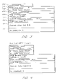
| Pre-test | Post-test | |
| Parameter | Measurement | Measurement |
| VOC (OPEN CIRCUIT VOLTAGE) | 2476 mV | 2476 mV |
| ISC (SHORT CIRCUIT CURRENT) | 360.5 mA | 359.0 mA |
| CFF (CURVE FIELD FACTOR) | 81.5% | 81.5% |
| Efficiency | 22.1% | 22% |
Claims (44)
Priority Applications (2)
| Application Number | Priority Date | Filing Date | Title |
|---|---|---|---|
| US10/336,247 US7115811B2 (en) | 1998-05-28 | 2003-01-03 | Semiconductor body forming a solar cell with a bypass diode |
| US11/100,066 US7449630B2 (en) | 1998-05-28 | 2005-04-06 | Solar cell having an integral monolithically grown bypass diode |
Applications Claiming Priority (4)
| Application Number | Priority Date | Filing Date | Title |
|---|---|---|---|
| US8720698P | 1998-05-28 | 1998-05-28 | |
| US09/314,597 US6278054B1 (en) | 1998-05-28 | 1999-05-19 | Solar cell having an integral monolithically grown bypass diode |
| US09/934,221 US6600100B2 (en) | 1998-05-28 | 2001-08-21 | Solar cell having an integral monolithically grown bypass diode |
| US10/336,247 US7115811B2 (en) | 1998-05-28 | 2003-01-03 | Semiconductor body forming a solar cell with a bypass diode |
Related Parent Applications (1)
| Application Number | Title | Priority Date | Filing Date |
|---|---|---|---|
| US09/934,221 Continuation US6600100B2 (en) | 1998-05-28 | 2001-08-21 | Solar cell having an integral monolithically grown bypass diode |
Related Child Applications (1)
| Application Number | Title | Priority Date | Filing Date |
|---|---|---|---|
| US11/100,066 Division US7449630B2 (en) | 1998-05-28 | 2005-04-06 | Solar cell having an integral monolithically grown bypass diode |
Publications (2)
| Publication Number | Publication Date |
|---|---|
| US20040040593A1 US20040040593A1 (en) | 2004-03-04 |
| US7115811B2 true US7115811B2 (en) | 2006-10-03 |
Family
ID=26776720
Family Applications (5)
| Application Number | Title | Priority Date | Filing Date |
|---|---|---|---|
| US09/314,597 Expired - Lifetime US6278054B1 (en) | 1998-05-28 | 1999-05-19 | Solar cell having an integral monolithically grown bypass diode |
| US09/753,492 Expired - Lifetime US6359210B2 (en) | 1998-05-28 | 2001-01-02 | Solar cell having an integral monolithically grown bypass diode |
| US09/934,221 Expired - Lifetime US6600100B2 (en) | 1998-05-28 | 2001-08-21 | Solar cell having an integral monolithically grown bypass diode |
| US10/336,247 Expired - Lifetime US7115811B2 (en) | 1998-05-28 | 2003-01-03 | Semiconductor body forming a solar cell with a bypass diode |
| US11/100,066 Expired - Fee Related US7449630B2 (en) | 1998-05-28 | 2005-04-06 | Solar cell having an integral monolithically grown bypass diode |
Family Applications Before (3)
| Application Number | Title | Priority Date | Filing Date |
|---|---|---|---|
| US09/314,597 Expired - Lifetime US6278054B1 (en) | 1998-05-28 | 1999-05-19 | Solar cell having an integral monolithically grown bypass diode |
| US09/753,492 Expired - Lifetime US6359210B2 (en) | 1998-05-28 | 2001-01-02 | Solar cell having an integral monolithically grown bypass diode |
| US09/934,221 Expired - Lifetime US6600100B2 (en) | 1998-05-28 | 2001-08-21 | Solar cell having an integral monolithically grown bypass diode |
Family Applications After (1)
| Application Number | Title | Priority Date | Filing Date |
|---|---|---|---|
| US11/100,066 Expired - Fee Related US7449630B2 (en) | 1998-05-28 | 2005-04-06 | Solar cell having an integral monolithically grown bypass diode |
Country Status (1)
| Country | Link |
|---|---|
| US (5) | US6278054B1 (en) |
Cited By (24)
| Publication number | Priority date | Publication date | Assignee | Title |
|---|---|---|---|---|
| US20060018583A1 (en) * | 2004-05-05 | 2006-01-26 | Iannelli John M | Method and apparatus for distortion control for optical transmitters |
| US20060210282A1 (en) * | 2005-03-15 | 2006-09-21 | John Iannelli | Directly modulated laser optical transmission system with phase modulation |
| US20070044832A1 (en) * | 2005-08-25 | 2007-03-01 | Fritzemeier Leslie G | Photovoltaic template |
| US20070095384A1 (en) * | 2005-10-28 | 2007-05-03 | Farquhar Donald S | Photovoltaic modules and interconnect methodology for fabricating the same |
| US20070206962A1 (en) * | 2006-03-02 | 2007-09-06 | Emcore Corporation | Externally modulated laser optical transmission system with feed forward noise cancellation |
| US20070206961A1 (en) * | 2006-03-02 | 2007-09-06 | Emcore Corporation | Directly modulated or externally modulated laser optical transmission system with feed forward noise cancellation |
| US20080072953A1 (en) * | 2006-09-27 | 2008-03-27 | Thinsilicon Corp. | Back contact device for photovoltaic cells and method of manufacturing a back contact device |
| US20080092943A1 (en) * | 2006-10-19 | 2008-04-24 | Emcore Corporation | Solar cell structure with localized doping in cap layer |
| US20080149173A1 (en) * | 2006-12-21 | 2008-06-26 | Sharps Paul R | Inverted metamorphic solar cell with bypass diode |
| US20080185038A1 (en) * | 2007-02-02 | 2008-08-07 | Emcore Corporation | Inverted metamorphic solar cell with via for backside contacts |
| US20090117679A1 (en) * | 2007-11-02 | 2009-05-07 | Fritzemeier Leslie G | Methods for forming crystalline thin-film photovoltaic structures |
| US20100078064A1 (en) * | 2008-09-29 | 2010-04-01 | Thinsilicion Corporation | Monolithically-integrated solar module |
| US20100233839A1 (en) * | 2009-01-29 | 2010-09-16 | Emcore Solar Power, Inc. | String Interconnection and Fabrication of Inverted Metamorphic Multijunction Solar Cells |
| US20100229913A1 (en) * | 2009-01-29 | 2010-09-16 | Emcore Solar Power, Inc. | Contact Layout and String Interconnection of Inverted Metamorphic Multijunction Solar Cells |
| US20100243038A1 (en) * | 2009-03-27 | 2010-09-30 | The Boeing Company | Solar cell assembly with combined handle substrate and bypass diode and method |
| US20100275969A1 (en) * | 2009-05-04 | 2010-11-04 | Microlink Devices, Inc. | Assembly techniques for solar cell arrays and solar cells formed therefrom |
| US20100313942A1 (en) * | 2009-06-10 | 2010-12-16 | Thinsilicion Corporation | Photovoltaic module and method of manufacturing a photovoltaic module having multiple semiconductor layer stacks |
| US8236603B1 (en) | 2008-09-04 | 2012-08-07 | Solexant Corp. | Polycrystalline semiconductor layers and methods for forming the same |
| US8415187B2 (en) | 2009-01-28 | 2013-04-09 | Solexant Corporation | Large-grain crystalline thin-film structures and devices and methods for forming the same |
| US8460964B2 (en) | 2010-11-17 | 2013-06-11 | E I Du Pont De Nemours And Company | Method for producing an array of thin-film photovoltaic cells having a totally separated integrated bypass diode and method for producing a panel incorporating the same |
| US8604330B1 (en) | 2010-12-06 | 2013-12-10 | 4Power, Llc | High-efficiency solar-cell arrays with integrated devices and methods for forming them |
| USRE44647E1 (en) | 2005-03-15 | 2013-12-17 | Emcore Corporation | Directly modulated laser optical transmission system with phase modulation |
| US9627565B2 (en) | 2013-11-27 | 2017-04-18 | Space Systems/Loral, Llc | Integral corner bypass diode interconnecting configuration for multiple solar cells |
| US10153388B1 (en) | 2013-03-15 | 2018-12-11 | Solaero Technologies Corp. | Emissivity coating for space solar cell arrays |
Families Citing this family (245)
| Publication number | Priority date | Publication date | Assignee | Title |
|---|---|---|---|---|
| US6278054B1 (en) * | 1998-05-28 | 2001-08-21 | Tecstar Power Systems, Inc. | Solar cell having an integral monolithically grown bypass diode |
| WO2002009187A2 (en) * | 2000-07-24 | 2002-01-31 | Motorola, Inc. | Heterojunction tunneling diodes and process for fabricating same |
| US6476314B2 (en) * | 2001-03-20 | 2002-11-05 | The Boeing Company | Solar tile and associated method for fabricating the same |
| WO2003010143A1 (en) * | 2001-07-26 | 2003-02-06 | Samsung Electronics Co., Ltd. | Dialkylhydroxybenzoic acid derivatives containing metal chelating groups and their therapeutic uses |
| JP3507828B2 (en) * | 2001-09-11 | 2004-03-15 | シャープ株式会社 | Heterojunction bipolar transistor and method of manufacturing the same |
| WO2003054926A2 (en) * | 2001-10-24 | 2003-07-03 | Emcore Corporation | An apparatus and method for integral bypass diode in solar cells |
| US6864414B2 (en) * | 2001-10-24 | 2005-03-08 | Emcore Corporation | Apparatus and method for integral bypass diode in solar cells |
| US6680432B2 (en) * | 2001-10-24 | 2004-01-20 | Emcore Corporation | Apparatus and method for optimizing the efficiency of a bypass diode in multijunction solar cells |
| DE10235048A1 (en) * | 2002-07-31 | 2004-02-12 | Astrium Gmbh | Solar cell connector with frame-shaped compensation section and method of manufacture |
| US7071407B2 (en) * | 2002-10-31 | 2006-07-04 | Emcore Corporation | Method and apparatus of multiplejunction solar cell structure with high band gap heterojunction middle cell |
| US6784358B2 (en) * | 2002-11-08 | 2004-08-31 | The Boeing Co. | Solar cell structure utilizing an amorphous silicon discrete by-pass diode |
| AU2003297649A1 (en) * | 2002-12-05 | 2004-06-30 | Blue Photonics, Inc. | High efficiency, monolithic multijunction solar cells containing lattice-mismatched materials and methods of forming same |
| US7535019B1 (en) | 2003-02-18 | 2009-05-19 | Nanosolar, Inc. | Optoelectronic fiber |
| US20050022857A1 (en) * | 2003-08-01 | 2005-02-03 | Daroczi Shandor G. | Solar cell interconnect structure |
| DE102004023856B4 (en) * | 2004-05-12 | 2006-07-13 | Rwe Space Solar Power Gmbh | Solar cell with integrated protection diode and additionally arranged on this tunnel diode |
| ITMI20041128A1 (en) * | 2004-06-04 | 2004-09-04 | Cesi Ct Elettrotecnico Sperime | PHOTOVOLTAIC CELL WITH PROTECTION DEVICE |
| DE102004044061A1 (en) * | 2004-09-11 | 2006-04-20 | Rwe Space Solar Power Gmbh | Solar cell arrangement and method for interconnecting a solar cell string |
| US7732706B1 (en) * | 2004-09-17 | 2010-06-08 | The United States Of America As Represented By The Administrator Of The National Aeronautics And Space Administration | Solar cell circuit and method for manufacturing solar cells |
| US8697987B2 (en) * | 2004-10-08 | 2014-04-15 | The Boeing Company | Solar cell having front grid metallization that does not contact the active layers |
| DE102004055225B4 (en) * | 2004-11-16 | 2014-07-31 | Fraunhofer-Gesellschaft zur Förderung der angewandten Forschung e.V. | Arrangement with solar cell and integrated bypass diode |
| US20060180198A1 (en) * | 2005-02-16 | 2006-08-17 | Sharp Kabushiki Kaisha | Solar cell, solar cell string and method of manufacturing solar cell string |
| US10374120B2 (en) * | 2005-02-18 | 2019-08-06 | Koninklijke Philips N.V. | High efficiency solar cells utilizing wafer bonding and layer transfer to integrate non-lattice matched materials |
| DE102005015132A1 (en) * | 2005-03-31 | 2006-10-05 | Rwe Space Solar Power Gmbh | solar cell |
| US20060231130A1 (en) * | 2005-04-19 | 2006-10-19 | Sharps Paul R | Solar cell with feedthrough via |
| US7906722B2 (en) * | 2005-04-19 | 2011-03-15 | Palo Alto Research Center Incorporated | Concentrating solar collector with solid optical element |
| US7196262B2 (en) * | 2005-06-20 | 2007-03-27 | Solyndra, Inc. | Bifacial elongated solar cell devices |
| US7394016B2 (en) * | 2005-10-11 | 2008-07-01 | Solyndra, Inc. | Bifacial elongated solar cell devices with internal reflectors |
| US8344238B2 (en) * | 2005-07-19 | 2013-01-01 | Solyndra Llc | Self-cleaning protective coatings for use with photovoltaic cells |
| EP1920468B1 (en) | 2005-09-01 | 2014-02-26 | Merck Patent GmbH | Photovoltaic cells integrated with bypass diode |
| US7542287B2 (en) | 2005-09-19 | 2009-06-02 | Chatsworth Products, Inc. | Air diverter for directing air upwardly in an equipment enclosure |
| US11259446B2 (en) | 2005-09-19 | 2022-02-22 | Chatsworth Products, Inc. | Vertical exhaust duct for electronic equipment enclosure |
| US11212928B2 (en) | 2005-09-19 | 2021-12-28 | Chatsworth Products, Inc. | Vertical exhaust duct for electronic equipment enclosure |
| US8107238B2 (en) | 2005-09-19 | 2012-01-31 | Chatsworth Products, Inc. | Ducted exhaust equipment enclosure |
| US7804685B2 (en) | 2005-09-19 | 2010-09-28 | Chatsworth Products, Inc. | Ducted exhaust equipment enclosure |
| US7732705B2 (en) * | 2005-10-11 | 2010-06-08 | Emcore Solar Power, Inc. | Reliable interconnection of solar cells including integral bypass diode |
| US7687707B2 (en) * | 2005-11-16 | 2010-03-30 | Emcore Solar Power, Inc. | Via structures in solar cells with bypass diode |
| US20070107773A1 (en) | 2005-11-17 | 2007-05-17 | Palo Alto Research Center Incorporated | Bifacial cell with extruded gridline metallization |
| US20070169806A1 (en) * | 2006-01-20 | 2007-07-26 | Palo Alto Research Center Incorporated | Solar cell production using non-contact patterning and direct-write metallization |
| US7765949B2 (en) | 2005-11-17 | 2010-08-03 | Palo Alto Research Center Incorporated | Extrusion/dispensing systems and methods |
| US7799371B2 (en) * | 2005-11-17 | 2010-09-21 | Palo Alto Research Center Incorporated | Extruding/dispensing multiple materials to form high-aspect ratio extruded structures |
| US9029685B2 (en) * | 2005-11-18 | 2015-05-12 | The Boeing Company | Monolithic bypass diode and photovoltaic cell with bypass diode formed in back of substrate |
| US11881814B2 (en) | 2005-12-05 | 2024-01-23 | Solaredge Technologies Ltd. | Testing of a photovoltaic panel |
| US10693415B2 (en) | 2007-12-05 | 2020-06-23 | Solaredge Technologies Ltd. | Testing of a photovoltaic panel |
| US7259322B2 (en) * | 2006-01-09 | 2007-08-21 | Solyndra, Inc. | Interconnects for solar cell devices |
| US20080302418A1 (en) * | 2006-03-18 | 2008-12-11 | Benyamin Buller | Elongated Photovoltaic Devices in Casings |
| US8183458B2 (en) | 2007-03-13 | 2012-05-22 | Solyndra Llc | Photovoltaic apparatus having a filler layer and method for making the same |
| US20090014055A1 (en) * | 2006-03-18 | 2009-01-15 | Solyndra, Inc. | Photovoltaic Modules Having a Filling Material |
| US20070215195A1 (en) * | 2006-03-18 | 2007-09-20 | Benyamin Buller | Elongated photovoltaic cells in tubular casings |
| US20070215197A1 (en) * | 2006-03-18 | 2007-09-20 | Benyamin Buller | Elongated photovoltaic cells in casings |
| JP5266205B2 (en) * | 2006-04-13 | 2013-08-21 | シェル・エルノイエルバーレ・エネルギエン・ゲーエムベーハー | Solar cell module |
| US7855335B2 (en) * | 2006-04-26 | 2010-12-21 | Palo Alto Research Center Incorporated | Beam integration for concentrating solar collector |
| US7851693B2 (en) * | 2006-05-05 | 2010-12-14 | Palo Alto Research Center Incorporated | Passively cooled solar concentrating photovoltaic device |
| US7638708B2 (en) * | 2006-05-05 | 2009-12-29 | Palo Alto Research Center Incorporated | Laminated solar concentrating photovoltaic device |
| US8536445B2 (en) | 2006-06-02 | 2013-09-17 | Emcore Solar Power, Inc. | Inverted metamorphic multijunction solar cells |
| US20070283997A1 (en) * | 2006-06-13 | 2007-12-13 | Miasole | Photovoltaic module with integrated current collection and interconnection |
| JP4290747B2 (en) * | 2006-06-23 | 2009-07-08 | シャープ株式会社 | Photoelectric conversion element and photoelectric conversion element with interconnector |
| US20080029152A1 (en) * | 2006-08-04 | 2008-02-07 | Erel Milshtein | Laser scribing apparatus, systems, and methods |
| US7879685B2 (en) * | 2006-08-04 | 2011-02-01 | Solyndra, Inc. | System and method for creating electric isolation between layers comprising solar cells |
| US8686282B2 (en) | 2006-08-07 | 2014-04-01 | Emcore Solar Power, Inc. | Solar power system for space vehicles or satellites using inverted metamorphic multijunction solar cells |
| US20080029151A1 (en) * | 2006-08-07 | 2008-02-07 | Mcglynn Daniel | Terrestrial solar power system using III-V semiconductor solar cells |
| US8148627B2 (en) * | 2006-08-25 | 2012-04-03 | Sunpower Corporation | Solar cell interconnect with multiple current paths |
| KR20080021428A (en) * | 2006-09-04 | 2008-03-07 | 엘지전자 주식회사 | Thin-film type solar cell including by-pass diode and manufacturing method thereof |
| US7922471B2 (en) | 2006-11-01 | 2011-04-12 | Palo Alto Research Center Incorporated | Extruded structure with equilibrium shape |
| US7780812B2 (en) | 2006-11-01 | 2010-08-24 | Palo Alto Research Center Incorporated | Extrusion head with planarized edge surface |
| US8322025B2 (en) * | 2006-11-01 | 2012-12-04 | Solarworld Innovations Gmbh | Apparatus for forming a plurality of high-aspect ratio gridline structures |
| US8226391B2 (en) | 2006-11-01 | 2012-07-24 | Solarworld Innovations Gmbh | Micro-extrusion printhead nozzle with tapered cross-section |
| US8816535B2 (en) | 2007-10-10 | 2014-08-26 | Solaredge Technologies, Ltd. | System and method for protection during inverter shutdown in distributed power installations |
| US11735910B2 (en) | 2006-12-06 | 2023-08-22 | Solaredge Technologies Ltd. | Distributed power system using direct current power sources |
| US8319483B2 (en) | 2007-08-06 | 2012-11-27 | Solaredge Technologies Ltd. | Digital average input current control in power converter |
| US11855231B2 (en) | 2006-12-06 | 2023-12-26 | Solaredge Technologies Ltd. | Distributed power harvesting systems using DC power sources |
| US11309832B2 (en) | 2006-12-06 | 2022-04-19 | Solaredge Technologies Ltd. | Distributed power harvesting systems using DC power sources |
| US11569659B2 (en) | 2006-12-06 | 2023-01-31 | Solaredge Technologies Ltd. | Distributed power harvesting systems using DC power sources |
| US11687112B2 (en) | 2006-12-06 | 2023-06-27 | Solaredge Technologies Ltd. | Distributed power harvesting systems using DC power sources |
| US8963369B2 (en) | 2007-12-04 | 2015-02-24 | Solaredge Technologies Ltd. | Distributed power harvesting systems using DC power sources |
| US11888387B2 (en) | 2006-12-06 | 2024-01-30 | Solaredge Technologies Ltd. | Safety mechanisms, wake up and shutdown methods in distributed power installations |
| US9130401B2 (en) | 2006-12-06 | 2015-09-08 | Solaredge Technologies Ltd. | Distributed power harvesting systems using DC power sources |
| US11728768B2 (en) | 2006-12-06 | 2023-08-15 | Solaredge Technologies Ltd. | Pairing of components in a direct current distributed power generation system |
| US8947194B2 (en) | 2009-05-26 | 2015-02-03 | Solaredge Technologies Ltd. | Theft detection and prevention in a power generation system |
| US8473250B2 (en) | 2006-12-06 | 2013-06-25 | Solaredge, Ltd. | Monitoring of distributed power harvesting systems using DC power sources |
| US8013472B2 (en) | 2006-12-06 | 2011-09-06 | Solaredge, Ltd. | Method for distributed power harvesting using DC power sources |
| US8618692B2 (en) | 2007-12-04 | 2013-12-31 | Solaredge Technologies Ltd. | Distributed power system using direct current power sources |
| US9112379B2 (en) | 2006-12-06 | 2015-08-18 | Solaredge Technologies Ltd. | Pairing of components in a direct current distributed power generation system |
| US11296650B2 (en) | 2006-12-06 | 2022-04-05 | Solaredge Technologies Ltd. | System and method for protection during inverter shutdown in distributed power installations |
| US8319471B2 (en) | 2006-12-06 | 2012-11-27 | Solaredge, Ltd. | Battery power delivery module |
| US8384243B2 (en) | 2007-12-04 | 2013-02-26 | Solaredge Technologies Ltd. | Distributed power harvesting systems using DC power sources |
| US9088178B2 (en) | 2006-12-06 | 2015-07-21 | Solaredge Technologies Ltd | Distributed power harvesting systems using DC power sources |
| US7638438B2 (en) * | 2006-12-12 | 2009-12-29 | Palo Alto Research Center Incorporated | Solar cell fabrication using extrusion mask |
| US7928015B2 (en) * | 2006-12-12 | 2011-04-19 | Palo Alto Research Center Incorporated | Solar cell fabrication using extruded dopant-bearing materials |
| US20100093127A1 (en) * | 2006-12-27 | 2010-04-15 | Emcore Solar Power, Inc. | Inverted Metamorphic Multijunction Solar Cell Mounted on Metallized Flexible Film |
| US20080245409A1 (en) * | 2006-12-27 | 2008-10-09 | Emcore Corporation | Inverted Metamorphic Solar Cell Mounted on Flexible Film |
| US20080178927A1 (en) * | 2007-01-30 | 2008-07-31 | Thomas Brezoczky | Photovoltaic apparatus having an elongated photovoltaic device using an involute-based concentrator |
| US8350417B1 (en) | 2007-01-30 | 2013-01-08 | Sunpower Corporation | Method and apparatus for monitoring energy consumption of a customer structure |
| US20080186593A1 (en) | 2007-02-02 | 2008-08-07 | Sol Focus, Inc. | Metal trace fabrication for optical element |
| US20080196759A1 (en) * | 2007-02-16 | 2008-08-21 | Thomas Brezoczky | Photovoltaic assembly with elongated photovoltaic devices and integrated involute-based reflectors |
| DE102007011403A1 (en) * | 2007-03-08 | 2008-09-11 | Fraunhofer-Gesellschaft zur Förderung der angewandten Forschung e.V. | Front side series connected solar module |
| US8158877B2 (en) * | 2007-03-30 | 2012-04-17 | Sunpower Corporation | Localized power point optimizer for solar cell installations |
| US7825328B2 (en) | 2007-04-09 | 2010-11-02 | Taiwan Semiconductor Manufacturing Company, Ltd. | Nitride-based multi-junction solar cell modules and methods for making the same |
| US7954449B2 (en) * | 2007-05-08 | 2011-06-07 | Palo Alto Research Center Incorporated | Wiring-free, plumbing-free, cooled, vacuum chuck |
| US7838062B2 (en) * | 2007-05-29 | 2010-11-23 | Sunpower Corporation | Array of small contacts for solar cell fabrication |
| US8697980B2 (en) * | 2007-06-19 | 2014-04-15 | Hanergy Holding Group Ltd. | Photovoltaic module utilizing an integrated flex circuit and incorporating a bypass diode |
| US20090014049A1 (en) * | 2007-07-13 | 2009-01-15 | Miasole | Photovoltaic module with integrated energy storage |
| US20090014058A1 (en) * | 2007-07-13 | 2009-01-15 | Miasole | Rooftop photovoltaic systems |
| US20090032090A1 (en) * | 2007-07-30 | 2009-02-05 | Emcore Corporation | Method for assembling a terrestrial solar array including a rigid support frame |
| US7381886B1 (en) * | 2007-07-30 | 2008-06-03 | Emcore Corporation | Terrestrial solar array |
| US20090038679A1 (en) * | 2007-08-09 | 2009-02-12 | Emcore Corporation | Thin Multijunction Solar Cells With Plated Metal OHMIC Contact and Support |
| US20100233838A1 (en) * | 2009-03-10 | 2010-09-16 | Emcore Solar Power, Inc. | Mounting of Solar Cells on a Flexible Substrate |
| US8895342B2 (en) | 2007-09-24 | 2014-11-25 | Emcore Solar Power, Inc. | Heterojunction subcells in inverted metamorphic multijunction solar cells |
| US10381505B2 (en) | 2007-09-24 | 2019-08-13 | Solaero Technologies Corp. | Inverted metamorphic multijunction solar cells including metamorphic layers |
| US20090078303A1 (en) * | 2007-09-24 | 2009-03-26 | Solyndra, Inc. | Encapsulated Photovoltaic Device Used With A Reflector And A Method of Use for the Same |
| US8614395B1 (en) * | 2007-11-01 | 2013-12-24 | Sandia Corporation | Solar cell with back side contacts |
| US8892738B2 (en) | 2007-11-07 | 2014-11-18 | Numecent Holdings, Inc. | Deriving component statistics for a stream enabled application |
| WO2009072076A2 (en) | 2007-12-05 | 2009-06-11 | Solaredge Technologies Ltd. | Current sensing on a mosfet |
| US11264947B2 (en) | 2007-12-05 | 2022-03-01 | Solaredge Technologies Ltd. | Testing of a photovoltaic panel |
| US20090188561A1 (en) * | 2008-01-25 | 2009-07-30 | Emcore Corporation | High concentration terrestrial solar array with III-V compound semiconductor cell |
| US20090188554A1 (en) * | 2008-01-25 | 2009-07-30 | Emcore Corporation | III-V Compound Semiconductor Solar Cell for Terrestrial Solar Array |
| US8513514B2 (en) * | 2008-10-24 | 2013-08-20 | Suncore Photovoltaics, Inc. | Solar tracking for terrestrial solar arrays with variable start and stop positions |
| DE102008008504A1 (en) * | 2008-02-11 | 2009-08-13 | Siemens Aktiengesellschaft | Method for theft detection of a PV module and failure detection of a bypass diode of a PV module as well as corresponding PV sub-generator junction box, PV inverter and corresponding PV system |
| US8759138B2 (en) | 2008-02-11 | 2014-06-24 | Suncore Photovoltaics, Inc. | Concentrated photovoltaic system modules using III-V semiconductor solar cells |
| US9331228B2 (en) | 2008-02-11 | 2016-05-03 | Suncore Photovoltaics, Inc. | Concentrated photovoltaic system modules using III-V semiconductor solar cells |
| US20110197947A1 (en) | 2008-03-20 | 2011-08-18 | Miasole | Wire network for interconnecting photovoltaic cells |
| US8912429B2 (en) * | 2008-03-20 | 2014-12-16 | Hanergy Holding Group Ltd. | Interconnect assembly |
| US20100043863A1 (en) | 2008-03-20 | 2010-02-25 | Miasole | Interconnect assembly |
| EP4145691A1 (en) | 2008-03-24 | 2023-03-08 | Solaredge Technologies Ltd. | Switch mode converter including auxiliary commutation circuit for achieving zero current switching |
| WO2009136358A1 (en) | 2008-05-05 | 2009-11-12 | Solaredge Technologies Ltd. | Direct current power combiner |
| US20090283137A1 (en) * | 2008-05-15 | 2009-11-19 | Steven Thomas Croft | Solar-cell module with in-laminate diodes and external-connection mechanisms mounted to respective edge regions |
| US20100012170A1 (en) * | 2008-07-20 | 2010-01-21 | Varonides Argyrios C | High Efficiency Solar Cell |
| US7999175B2 (en) | 2008-09-09 | 2011-08-16 | Palo Alto Research Center Incorporated | Interdigitated back contact silicon solar cells with laser ablated grooves |
| US8062693B2 (en) * | 2008-09-22 | 2011-11-22 | Sunpower Corporation | Generation of contact masks for inkjet printing on solar cell substrates |
| US8866005B2 (en) * | 2008-10-17 | 2014-10-21 | Kopin Corporation | InGaP heterojunction barrier solar cells |
| EP2345088A2 (en) * | 2008-10-23 | 2011-07-20 | Alta Devices, Inc. | Integration of a photovoltaic device |
| TW201029195A (en) * | 2008-10-23 | 2010-08-01 | Alta Devices Inc | Photovoltaic device with back side contacts |
| US20120104460A1 (en) | 2010-11-03 | 2012-05-03 | Alta Devices, Inc. | Optoelectronic devices including heterojunction |
| TW201030998A (en) | 2008-10-23 | 2010-08-16 | Alta Devices Inc | Photovoltaic device |
| WO2010048543A2 (en) * | 2008-10-23 | 2010-04-29 | Alta Devices, Inc. | Thin absorber layer of a photovoltaic device |
| WO2010048547A2 (en) * | 2008-10-23 | 2010-04-29 | Alta Devices, Inc. | Photovoltaic device with increased light trapping |
| US8507837B2 (en) * | 2008-10-24 | 2013-08-13 | Suncore Photovoltaics, Inc. | Techniques for monitoring solar array performance and applications thereof |
| US9059351B2 (en) | 2008-11-04 | 2015-06-16 | Apollo Precision (Fujian) Limited | Integrated diode assemblies for photovoltaic modules |
| US8586857B2 (en) * | 2008-11-04 | 2013-11-19 | Miasole | Combined diode, lead assembly incorporating an expansion joint |
| US8117983B2 (en) * | 2008-11-07 | 2012-02-21 | Solarworld Innovations Gmbh | Directional extruded bead control |
| US20100117254A1 (en) * | 2008-11-07 | 2010-05-13 | Palo Alto Research Center Incorporated | Micro-Extrusion System With Airjet Assisted Bead Deflection |
| US8080729B2 (en) | 2008-11-24 | 2011-12-20 | Palo Alto Research Center Incorporated | Melt planarization of solar cell bus bars |
| US8960120B2 (en) | 2008-12-09 | 2015-02-24 | Palo Alto Research Center Incorporated | Micro-extrusion printhead with nozzle valves |
| US9608149B2 (en) * | 2008-12-19 | 2017-03-28 | Sphelar Power Corporation | Solar cell module and method for producing the same |
| US9105783B2 (en) * | 2009-01-26 | 2015-08-11 | The Aerospace Corporation | Holographic solar concentrator |
| US8409911B2 (en) * | 2009-02-24 | 2013-04-02 | Sunpower Corporation | Methods for metallization of solar cells |
| EP2602831B1 (en) | 2009-05-22 | 2014-07-16 | Solaredge Technologies Ltd. | Electrically isolated heat dissipating junction box |
| US20110168236A1 (en) * | 2009-06-16 | 2011-07-14 | Winston Kong Chan | Portable photovoltaics with scalable integrated concentrator of light energy |
| US20110048505A1 (en) * | 2009-08-27 | 2011-03-03 | Gabriela Bunea | Module Level Solution to Solar Cell Polarization Using an Encapsulant with Opened UV Transmission Curve |
| US20110048488A1 (en) * | 2009-09-01 | 2011-03-03 | Gabriel Karim M | Combined thermoelectric/photovoltaic device and method of making the same |
| US20110048489A1 (en) * | 2009-09-01 | 2011-03-03 | Gabriel Karim M | Combined thermoelectric/photovoltaic device for high heat flux applications and method of making the same |
| US9806215B2 (en) | 2009-09-03 | 2017-10-31 | Suncore Photovoltaics, Inc. | Encapsulated concentrated photovoltaic system subassembly for III-V semiconductor solar cells |
| US9012771B1 (en) | 2009-09-03 | 2015-04-21 | Suncore Photovoltaics, Inc. | Solar cell receiver subassembly with a heat shield for use in a concentrating solar system |
| US9691921B2 (en) | 2009-10-14 | 2017-06-27 | Alta Devices, Inc. | Textured metallic back reflector |
| ES2400634B2 (en) * | 2009-10-20 | 2013-12-03 | Suncore Photovoltaics Inc. | CONCENTRATION PHOTOVOLTAIC SYSTEM MODULES USING SOLAR SEMICONDUCTOR CELLS III-V. |
| US9502594B2 (en) | 2012-01-19 | 2016-11-22 | Alta Devices, Inc. | Thin-film semiconductor optoelectronic device with textured front and/or back surface prepared from template layer and etching |
| US11271128B2 (en) | 2009-10-23 | 2022-03-08 | Utica Leaseco, Llc | Multi-junction optoelectronic device |
| US9768329B1 (en) | 2009-10-23 | 2017-09-19 | Alta Devices, Inc. | Multi-junction optoelectronic device |
| US20170141256A1 (en) | 2009-10-23 | 2017-05-18 | Alta Devices, Inc. | Multi-junction optoelectronic device with group iv semiconductor as a bottom junction |
| US20150380576A1 (en) | 2010-10-13 | 2015-12-31 | Alta Devices, Inc. | Optoelectronic device with dielectric layer and method of manufacture |
| US9337360B1 (en) * | 2009-11-16 | 2016-05-10 | Solar Junction Corporation | Non-alloyed contacts for III-V based solar cells |
| US8356640B1 (en) | 2010-01-14 | 2013-01-22 | Mia Solé | Apparatuses and methods for fabricating wire current collectors and interconnects for solar cells |
| US9214586B2 (en) * | 2010-04-30 | 2015-12-15 | Solar Junction Corporation | Semiconductor solar cell package |
| US20110265857A1 (en) * | 2010-05-03 | 2011-11-03 | DuPont Apollo Ltd. | Monolithic integration of bypass diodes with a thin film solar module |
| US9061344B1 (en) | 2010-05-26 | 2015-06-23 | Apollo Precision (Fujian) Limited | Apparatuses and methods for fabricating wire current collectors and interconnects for solar cells |
| EP2395563A1 (en) * | 2010-06-10 | 2011-12-14 | Megawatt Solar, Inc. | Receivers for Concentrating Photovoltaic Systems and Methods for Fabricating the Same |
| US8377738B2 (en) | 2010-07-01 | 2013-02-19 | Sunpower Corporation | Fabrication of solar cells with counter doping prevention |
| US8426974B2 (en) | 2010-09-29 | 2013-04-23 | Sunpower Corporation | Interconnect for an optoelectronic device |
| US10026859B2 (en) | 2010-10-04 | 2018-07-17 | Beijing Apollo Ding Rong Solar Technology Co., Ltd. | Small gauge wire solar cell interconnect |
| GB2485527B (en) | 2010-11-09 | 2012-12-19 | Solaredge Technologies Ltd | Arc detection and prevention in a power generation system |
| US10230310B2 (en) | 2016-04-05 | 2019-03-12 | Solaredge Technologies Ltd | Safety switch for photovoltaic systems |
| US10673229B2 (en) | 2010-11-09 | 2020-06-02 | Solaredge Technologies Ltd. | Arc detection and prevention in a power generation system |
| US10673222B2 (en) | 2010-11-09 | 2020-06-02 | Solaredge Technologies Ltd. | Arc detection and prevention in a power generation system |
| US20120295395A1 (en) * | 2010-11-17 | 2012-11-22 | E.I. Du Pont De Nemours And Company | Method for producing an array of thin-film photovoltaic cells having a totally separated integrated bypass diode associated with a plurality of cells and method for producing a panel incorporating the same |
| US8884156B2 (en) | 2010-11-29 | 2014-11-11 | Palo Alto Research Center Incorporated | Solar energy harvesting device using stimuli-responsive material |
| US8040609B1 (en) | 2010-11-29 | 2011-10-18 | Palo Alto Research Center Incorporated | Self-adjusting solar light transmission apparatus |
| GB2486408A (en) | 2010-12-09 | 2012-06-20 | Solaredge Technologies Ltd | Disconnection of a string carrying direct current |
| US9083121B2 (en) | 2010-12-17 | 2015-07-14 | Sunpower Corporation | Diode-included connector, photovoltaic laminate and photovoltaic assembly using same |
| US9029689B2 (en) | 2010-12-23 | 2015-05-12 | Sunpower Corporation | Method for connecting solar cells |
| US8173452B1 (en) | 2010-12-29 | 2012-05-08 | Twin Creeks Technologies, Inc. | Method to form a device by constructing a support element on a thin semiconductor lamina |
| US8268645B2 (en) | 2010-12-29 | 2012-09-18 | Twin Creeks Technologies, Inc. | Method and apparatus for forming a thin lamina |
| US8536448B2 (en) | 2010-12-29 | 2013-09-17 | Gtat Corporation | Zener diode within a diode structure providing shunt protection |
| US8435804B2 (en) | 2010-12-29 | 2013-05-07 | Gtat Corporation | Method and apparatus for forming a thin lamina |
| GB2483317B (en) | 2011-01-12 | 2012-08-22 | Solaredge Technologies Ltd | Serially connected inverters |
| US8859892B2 (en) | 2011-02-03 | 2014-10-14 | Solar Junction Corporation | Integrated semiconductor solar cell package |
| US8962988B2 (en) | 2011-02-03 | 2015-02-24 | Solar Junction Corporation | Integrated semiconductor solar cell package |
| US9716196B2 (en) | 2011-02-09 | 2017-07-25 | Alta Devices, Inc. | Self-bypass diode function for gallium arsenide photovoltaic devices |
| US11121272B2 (en) | 2011-02-09 | 2021-09-14 | Utica Leaseco, Llc | Self-bypass diode function for gallium arsenide photovoltaic devices |
| US9502897B2 (en) | 2011-02-12 | 2016-11-22 | SolarBread LTD | Systems and methods for photovoltaic micro-inverter power harvesting efficiency increase in shaded conditions |
| US8951824B1 (en) | 2011-04-08 | 2015-02-10 | Apollo Precision (Fujian) Limited | Adhesives for attaching wire network to photovoltaic cells |
| CA2834131A1 (en) * | 2011-05-02 | 2012-11-08 | Mcmaster University | Areal current matching of tandem solar cells |
| EP2528097A1 (en) * | 2011-05-27 | 2012-11-28 | Nederlandse Organisatie voor toegepast -natuurwetenschappelijk onderzoek TNO | Photovoltaic device and method of manufacturing the same |
| US20120318318A1 (en) * | 2011-06-17 | 2012-12-20 | Solopower, Inc. | Cigs based thin film solar cells having shared bypass diodes |
| DE102011115659A1 (en) * | 2011-09-28 | 2013-03-28 | Osram Opto Semiconductors Gmbh | Photovoltaic semiconductor chip |
| DE102011119467A1 (en) | 2011-11-25 | 2013-05-29 | Fraunhofer-Gesellschaft zur Förderung der angewandten Forschung e.V. | Solar cell module and concentrator module and their use |
| RU2479888C1 (en) * | 2011-11-29 | 2013-04-20 | Открытое акционерное общество "Российская корпорация ракетно-космического приборостроения и информационных систем" (ОАО "Российские космические системы") | Method to manufacture shunting diode for solar batteries of spacecrafts |
| GB2498365A (en) | 2012-01-11 | 2013-07-17 | Solaredge Technologies Ltd | Photovoltaic module |
| US11038080B2 (en) | 2012-01-19 | 2021-06-15 | Utica Leaseco, Llc | Thin-film semiconductor optoelectronic device with textured front and/or back surface prepared from etching |
| GB2498791A (en) | 2012-01-30 | 2013-07-31 | Solaredge Technologies Ltd | Photovoltaic panel circuitry |
| GB2498790A (en) | 2012-01-30 | 2013-07-31 | Solaredge Technologies Ltd | Maximising power in a photovoltaic distributed power system |
| US9853565B2 (en) | 2012-01-30 | 2017-12-26 | Solaredge Technologies Ltd. | Maximized power in a photovoltaic distributed power system |
| US8581242B2 (en) * | 2012-02-21 | 2013-11-12 | Atomic Energy Council—Institute of Nuclear Energy Research | Apparatus combining bypass diode and wire |
| GB2499991A (en) | 2012-03-05 | 2013-09-11 | Solaredge Technologies Ltd | DC link circuit for photovoltaic array |
| US8884157B2 (en) * | 2012-05-11 | 2014-11-11 | Epistar Corporation | Method for manufacturing optoelectronic devices |
| US8752380B2 (en) | 2012-05-22 | 2014-06-17 | Palo Alto Research Center Incorporated | Collapsible solar-thermal concentrator for renewable, sustainable expeditionary power generator system |
| US10115841B2 (en) | 2012-06-04 | 2018-10-30 | Solaredge Technologies Ltd. | Integrated photovoltaic panel circuitry |
| RU2515420C2 (en) * | 2012-08-16 | 2014-05-10 | Открытое акционерное общество "Сатурн" | Method of making photoconverter with integrated diode |
| WO2014062850A1 (en) | 2012-10-16 | 2014-04-24 | Solexel, Inc. | Systems and methods for monolithically integrated bypass switches in photovoltaic solar cells and modules |
| US20140102529A1 (en) * | 2012-10-17 | 2014-04-17 | Emcore Solar Power, Inc. | Solar cell interconnect assembly and method for manufacturing the same |
| US9812590B2 (en) | 2012-10-25 | 2017-11-07 | Sunpower Corporation | Bifacial solar cell module with backside reflector |
| TWI524551B (en) * | 2012-11-19 | 2016-03-01 | 新世紀光電股份有限公司 | Nitride semiconductor structure and semiconductor light-emitting element |
| TWI499080B (en) | 2012-11-19 | 2015-09-01 | Genesis Photonics Inc | Nitride semiconductor structure and semiconductor light-emitting element |
| TWI535055B (en) | 2012-11-19 | 2016-05-21 | 新世紀光電股份有限公司 | Nitride semiconductor structure and semiconductor light-emitting element |
| US9035172B2 (en) | 2012-11-26 | 2015-05-19 | Sunpower Corporation | Crack resistant solar cell modules |
| US8796061B2 (en) | 2012-12-21 | 2014-08-05 | Sunpower Corporation | Module assembly for thin solar cells |
| US9548619B2 (en) | 2013-03-14 | 2017-01-17 | Solaredge Technologies Ltd. | Method and apparatus for storing and depleting energy |
| EP3506370B1 (en) | 2013-03-15 | 2023-12-20 | Solaredge Technologies Ltd. | Bypass mechanism |
| FR3004002B1 (en) * | 2013-03-29 | 2016-09-02 | Soitec Silicon On Insulator | PROCESS FOR ADVANCED ASSEMBLY OF CONCENTRATED PHOTOVOLTAIC CELL |
| US20150236638A1 (en) * | 2013-04-13 | 2015-08-20 | Solexel, Inc. | Solar photovoltaic module power control and status monitoring system utilizing laminateembedded remote access module switch |
| US10784815B2 (en) | 2013-04-13 | 2020-09-22 | Sigmagen, Inc. | Solar photovoltaic module remote access module switch and real-time temperature monitoring |
| US20150101761A1 (en) * | 2013-05-12 | 2015-04-16 | Solexel, Inc. | Solar photovoltaic blinds and curtains for residential and commercial buildings |
| US9685571B2 (en) | 2013-08-14 | 2017-06-20 | Sunpower Corporation | Solar cell module with high electric susceptibility layer |
| US20150048497A1 (en) * | 2013-08-16 | 2015-02-19 | Qualcomm Incorporated | Interposer with electrostatic discharge protection |
| DE102015002513A1 (en) | 2015-03-02 | 2016-09-08 | Azur Space Solar Power Gmbh | solar cell device |
| CN107408632B (en) * | 2015-03-31 | 2020-01-14 | 株式会社钟化 | Photoelectric conversion device and photoelectric conversion module |
| US20170040479A1 (en) | 2015-08-07 | 2017-02-09 | Solaero Technologies Corp. | Reliable interconnection of solar cells |
| CN105336749B (en) * | 2015-10-14 | 2018-05-08 | 天津三安光电有限公司 | Upside-down mounting multijunction solar cell chip of integrated bypass diode and preparation method thereof |
| US10090420B2 (en) | 2016-01-22 | 2018-10-02 | Solar Junction Corporation | Via etch method for back contact multijunction solar cells |
| CN107153212B (en) | 2016-03-03 | 2023-07-28 | 太阳能安吉科技有限公司 | Method for mapping a power generation facility |
| US10599113B2 (en) | 2016-03-03 | 2020-03-24 | Solaredge Technologies Ltd. | Apparatus and method for determining an order of power devices in power generation systems |
| US11081608B2 (en) | 2016-03-03 | 2021-08-03 | Solaredge Technologies Ltd. | Apparatus and method for determining an order of power devices in power generation systems |
| US11018623B2 (en) | 2016-04-05 | 2021-05-25 | Solaredge Technologies Ltd. | Safety switch for photovoltaic systems |
| US11177663B2 (en) | 2016-04-05 | 2021-11-16 | Solaredge Technologies Ltd. | Chain of power devices |
| US9680035B1 (en) | 2016-05-27 | 2017-06-13 | Solar Junction Corporation | Surface mount solar cell with integrated coverglass |
| US10128391B2 (en) | 2016-06-22 | 2018-11-13 | Beijing Apollo Ding Rong Solar Technology Co., Ltd. | Photovoltaic module with flexible wire interconnection |
| CN107068786A (en) * | 2016-12-28 | 2017-08-18 | 中国电子科技集团公司第十八研究所 | The structure design and manufacture method of solar cell integrated form binode diode |
| CN107068787A (en) * | 2016-12-28 | 2017-08-18 | 中国电子科技集团公司第十八研究所 | The structure design and manufacture method of solar cell integrated form GaAs junction diodes |
| KR101883759B1 (en) * | 2017-04-25 | 2018-07-31 | 엘지전자 주식회사 | Compound semiconductor solar cell and method for manufacturing the same |
| USD845889S1 (en) | 2018-01-16 | 2019-04-16 | Solaero Technologies Corp. | Flexible interconnecting member for solar cells |
| US10529881B2 (en) | 2018-03-01 | 2020-01-07 | Solaero Technologies Corp. | Interconnect member |
| CN109768104B (en) * | 2018-12-28 | 2021-02-19 | 中国电子科技集团公司第十八研究所 | Self-protection type integrated diode battery structure and preparation method thereof |
| US11271126B2 (en) | 2019-03-21 | 2022-03-08 | Beijing Apollo Ding Rong Solar Technology Co., Ltd. | Photovoltaic panels with folded panel edges and methods of forming the same |
| US11081252B2 (en) * | 2019-03-27 | 2021-08-03 | The United States Of America As Represented By The Secretary Of The Army | Electrophoretic deposition (EPD) of radioisotope and phosphor composite layer for hybrid radioisotope batteries and radioluminescent surfaces |
| US11563137B2 (en) | 2019-09-16 | 2023-01-24 | Meta Platforms Technologies, Llc | Optical transformer |
| US11431236B2 (en) | 2020-08-18 | 2022-08-30 | Meta Platforms Technologies, Llc | Dynamically addressable high voltage optical transformer with integrated optically triggered switches |
| EP4064368A1 (en) | 2021-03-24 | 2022-09-28 | Sunpower Corporation | Cross-tied photovoltaic array |
Citations (18)
| Publication number | Priority date | Publication date | Assignee | Title |
|---|---|---|---|---|
| US4083063A (en) * | 1973-10-09 | 1978-04-04 | General Electric Company | Gate turnoff thyristor with a pilot scr |
| JPS60160181A (en) * | 1984-01-30 | 1985-08-21 | Mitsubishi Electric Corp | Amorphous solar cell |
| US4759803A (en) * | 1987-08-07 | 1988-07-26 | Applied Solar Energy Corporation | Monolithic solar cell and bypass diode system |
| US5009720A (en) * | 1988-11-16 | 1991-04-23 | Mitsubishi Denki Kabushiki Kaisha | Solar cell |
| US5405453A (en) * | 1993-11-08 | 1995-04-11 | Applied Solar Energy Corporation | High efficiency multi-junction solar cell |
| WO1996018213A1 (en) * | 1994-12-08 | 1996-06-13 | Pacific Solar Pty. Limited | Multilayer solar cells with bypass diode protection |
| JPH0964397A (en) * | 1995-08-29 | 1997-03-07 | Canon Inc | Solar cell and solar cell module |
| US5616185A (en) * | 1995-10-10 | 1997-04-01 | Hughes Aircraft Company | Solar cell with integrated bypass diode and method |
| GB2346010A (en) * | 1999-01-25 | 2000-07-26 | Marconi Applied Technologies | Solar cell arrangements |
| US6278054B1 (en) * | 1998-05-28 | 2001-08-21 | Tecstar Power Systems, Inc. | Solar cell having an integral monolithically grown bypass diode |
| US6316716B1 (en) * | 1999-05-11 | 2001-11-13 | Angewandte Solarenergie - Ase Gmbh | Solar cell and method for producing such a cell |
| US6326540B1 (en) * | 1998-08-20 | 2001-12-04 | Tecstar Power Systems, Inc. | Solar cell having a front-mounted bypass diode |
| US20020040727A1 (en) * | 2000-06-20 | 2002-04-11 | Stan Mark A. | Apparatus and method for optimizing the efficiency of germanium junctions in multi-junction solar cells |
| US6452086B1 (en) * | 1998-10-05 | 2002-09-17 | Astrium Gmbh | Solar cell comprising a bypass diode |
| US20020164834A1 (en) * | 1999-07-14 | 2002-11-07 | Boutros Karim S. | Monolithic bypass-diode and solar-cell string assembly |
| US20030140962A1 (en) * | 2001-10-24 | 2003-07-31 | Sharps Paul R. | Apparatus and method for integral bypass diode in solar cells |
| US6680432B2 (en) * | 2001-10-24 | 2004-01-20 | Emcore Corporation | Apparatus and method for optimizing the efficiency of a bypass diode in multijunction solar cells |
| US20040166681A1 (en) * | 2002-12-05 | 2004-08-26 | Iles Peter A. | High efficiency, monolithic multijunction solar cells containing lattice-mismatched materials and methods of forming same |
Family Cites Families (50)
| Publication number | Priority date | Publication date | Assignee | Title |
|---|---|---|---|---|
| US3489615A (en) | 1966-07-05 | 1970-01-13 | Spectrolab | Solar cells with insulated wraparound electrodes |
| GB1382072A (en) | 1972-02-03 | 1975-01-29 | Ferranti Ltd | Solar cells |
| US3899689A (en) | 1972-05-25 | 1975-08-12 | Massachusetts Inst Technology | Electric power source |
| DE2253830C3 (en) | 1972-11-03 | 1983-06-16 | Licentia Patent-Verwaltungs-Gmbh, 6000 Frankfurt | Method for manufacturing a solar cell and a solar cell battery |
| DE2253831C3 (en) | 1972-11-03 | 1981-01-22 | Licentia Patent-Verwaltungs-Gmbh, 6000 Frankfurt | Solar cell battery |
| US4195621A (en) | 1977-12-27 | 1980-04-01 | Richdel, Inc. | Solid state differential temperature regulator for a solar heating system |
| US4133698A (en) | 1977-12-27 | 1979-01-09 | Texas Instruments Incorporated | Tandem junction solar cell |
| JPS5664475A (en) | 1979-08-23 | 1981-06-01 | Unisearch Ltd | Solar battery with branching diode |
| US4281278A (en) | 1979-12-05 | 1981-07-28 | Rca Corporation | Redundant battery protection system |
| US4361950A (en) | 1980-03-24 | 1982-12-07 | Exxon Research & Engineering Co. | Method of making solar cell with wrap-around electrode |
| US4322571A (en) | 1980-07-17 | 1982-03-30 | The Boeing Company | Solar cells and methods for manufacture thereof |
| US4367365A (en) | 1981-07-13 | 1983-01-04 | Acurex Solar Corporation | Solar energy conversion arrangement utilizing photovoltaic members |
| US4481378A (en) | 1982-07-30 | 1984-11-06 | Motorola, Inc. | Protected photovoltaic module |
| DE3307202A1 (en) | 1983-03-01 | 1984-09-06 | Siemens AG, 1000 Berlin und 8000 München | SOLAR CELL MODULE |
| US4610077A (en) | 1984-04-30 | 1986-09-09 | Hughes Aircraft Company | Process for fabricating a wraparound contact solar cell |
| US4577051A (en) | 1984-09-28 | 1986-03-18 | The Standard Oil Company | Bypass diode assembly for photovoltaic modules |
| US4612408A (en) | 1984-10-22 | 1986-09-16 | Sera Solar Corporation | Electrically isolated semiconductor integrated photodiode circuits and method |
| US4776893A (en) | 1985-06-03 | 1988-10-11 | Chevron Research Company | GaAs on GaSb mechanically stacked photovoltaic cells, package assembly, and modules |
| US4771017A (en) | 1987-06-23 | 1988-09-13 | Spire Corporation | Patterning process |
| US4824489A (en) | 1988-02-02 | 1989-04-25 | Sera Solar Corporation | Ultra-thin solar cell and method |
| US4909856A (en) | 1988-08-22 | 1990-03-20 | Hughes Aircraft Company | Composite coverglass for solar cell |
| EP0369635A3 (en) | 1988-11-12 | 1992-03-04 | British Aerospace Public Limited Company | Power supplies |
| US4933022A (en) | 1988-11-14 | 1990-06-12 | Board Of Trustees Of The Leland Stanford Univ. & Electric Power Research Institute | Solar cell having interdigitated contacts and internal bypass diodes |
| JPH02135786A (en) * | 1988-11-16 | 1990-05-24 | Mitsubishi Electric Corp | Solar battery cell |
| EP0373235A1 (en) | 1988-12-12 | 1990-06-20 | Siemens Aktiengesellschaft | Solar cell array |
| US4915744A (en) * | 1989-02-03 | 1990-04-10 | Applied Solar Energy Corporation | High efficiency solar cell |
| US5248346A (en) | 1989-04-17 | 1993-09-28 | The Boeing Company | Photovoltaic cell and array with inherent bypass diode |
| US5389158A (en) | 1989-04-17 | 1995-02-14 | The Boeing Company | Low bandgap photovoltaic cell with inherent bypass diode |
| US5011544A (en) | 1989-09-08 | 1991-04-30 | Solarex Corporation | Solar panel with interconnects and masking structure, and method |
| US5138403A (en) | 1989-10-27 | 1992-08-11 | Kopin Corporation | High temperature Schottky barrier bypass diodes |
| US5131341A (en) | 1990-12-03 | 1992-07-21 | Edwin Newman | Solar powered electric ship system |
| US5223043A (en) | 1991-02-11 | 1993-06-29 | The United States Of America As Represented By The United States Department Of Energy | Current-matched high-efficiency, multijunction monolithic solar cells |
| JP2912496B2 (en) | 1991-09-30 | 1999-06-28 | シャープ株式会社 | Solar cell module |
| JP2837296B2 (en) | 1991-10-17 | 1998-12-14 | シャープ株式会社 | Solar cell |
| US5230746A (en) | 1992-03-03 | 1993-07-27 | Amoco Corporation | Photovoltaic device having enhanced rear reflecting contact |
| US5391235A (en) | 1992-03-31 | 1995-02-21 | Canon Kabushiki Kaisha | Solar cell module and method of manufacturing the same |
| US5342453A (en) | 1992-11-13 | 1994-08-30 | Midwest Research Institute | Heterojunction solar cell |
| FR2701786B1 (en) | 1993-02-17 | 1995-09-22 | Europ Agence Spatiale | PHOTOVOLTAUIC CELL, ITS MANUFACTURING METHOD, AND SOLAR PANEL COMPRISING SUCH CELLS. |
| JPH0758355A (en) | 1993-05-12 | 1995-03-03 | Optical Coating Lab Inc | Uv / ir reflection solar cell cover |
| EP0681335B1 (en) | 1993-09-30 | 2001-11-28 | Canon Kabushiki Kaisha | Solar cell module having surface coating material of three-layer structure |
| US5498297A (en) | 1994-09-15 | 1996-03-12 | Entech, Inc. | Photovoltaic receiver |
| US5514223A (en) | 1995-02-17 | 1996-05-07 | United Solar Systems Corporation | Dual discharge photovoltaic module |
| US5753319A (en) | 1995-03-08 | 1998-05-19 | Corion Corporation | Method for ion plating deposition |
| FR2732170B1 (en) | 1995-03-24 | 1997-05-09 | Guyonneau Claude | HIGH VOLTAGE PHOTOVOLTAIC ENERGY STATION WITH PERSONALIZED STORAGE |
| US5567248A (en) | 1995-09-05 | 1996-10-22 | Chung; Darius | Modular solar cell contact arrangement |
| GB9525111D0 (en) | 1995-12-08 | 1996-02-07 | Pilkington Plc | Glass and glass products |
| US5741370A (en) | 1996-06-27 | 1998-04-21 | Evergreen Solar, Inc. | Solar cell modules with improved backskin and methods for forming same |
| US6121541A (en) * | 1997-07-28 | 2000-09-19 | Bp Solarex | Monolithic multi-junction solar cells with amorphous silicon and CIS and their alloys |
| WO1999062125A1 (en) * | 1998-05-28 | 1999-12-02 | Tecstar Power Systems, Inc. | Solar cell having an integral monolithically grown bypass diode |
| JP3888860B2 (en) * | 2000-05-24 | 2007-03-07 | シャープ株式会社 | Solar cell protection method |
-
1999
- 1999-05-19 US US09/314,597 patent/US6278054B1/en not_active Expired - Lifetime
-
2001
- 2001-01-02 US US09/753,492 patent/US6359210B2/en not_active Expired - Lifetime
- 2001-08-21 US US09/934,221 patent/US6600100B2/en not_active Expired - Lifetime
-
2003
- 2003-01-03 US US10/336,247 patent/US7115811B2/en not_active Expired - Lifetime
-
2005
- 2005-04-06 US US11/100,066 patent/US7449630B2/en not_active Expired - Fee Related
Patent Citations (24)
| Publication number | Priority date | Publication date | Assignee | Title |
|---|---|---|---|---|
| US4083063A (en) * | 1973-10-09 | 1978-04-04 | General Electric Company | Gate turnoff thyristor with a pilot scr |
| JPS60160181A (en) * | 1984-01-30 | 1985-08-21 | Mitsubishi Electric Corp | Amorphous solar cell |
| US4759803A (en) * | 1987-08-07 | 1988-07-26 | Applied Solar Energy Corporation | Monolithic solar cell and bypass diode system |
| US5009720A (en) * | 1988-11-16 | 1991-04-23 | Mitsubishi Denki Kabushiki Kaisha | Solar cell |
| US5405453A (en) * | 1993-11-08 | 1995-04-11 | Applied Solar Energy Corporation | High efficiency multi-junction solar cell |
| WO1996018213A1 (en) * | 1994-12-08 | 1996-06-13 | Pacific Solar Pty. Limited | Multilayer solar cells with bypass diode protection |
| JPH0964397A (en) * | 1995-08-29 | 1997-03-07 | Canon Inc | Solar cell and solar cell module |
| US5616185A (en) * | 1995-10-10 | 1997-04-01 | Hughes Aircraft Company | Solar cell with integrated bypass diode and method |
| US6359210B2 (en) * | 1998-05-28 | 2002-03-19 | Tecstar Power System, Inc. | Solar cell having an integral monolithically grown bypass diode |
| US20040040593A1 (en) * | 1998-05-28 | 2004-03-04 | Frank Ho | Solar cell having an integral monolithically grown bypass diode |
| US20050183765A1 (en) * | 1998-05-28 | 2005-08-25 | Frank Ho | Solar cell having an integral monolithically grown bypass diode |
| US6278054B1 (en) * | 1998-05-28 | 2001-08-21 | Tecstar Power Systems, Inc. | Solar cell having an integral monolithically grown bypass diode |
| US6600100B2 (en) * | 1998-05-28 | 2003-07-29 | Emcore Corporation | Solar cell having an integral monolithically grown bypass diode |
| US6326540B1 (en) * | 1998-08-20 | 2001-12-04 | Tecstar Power Systems, Inc. | Solar cell having a front-mounted bypass diode |
| US6452086B1 (en) * | 1998-10-05 | 2002-09-17 | Astrium Gmbh | Solar cell comprising a bypass diode |
| GB2346010A (en) * | 1999-01-25 | 2000-07-26 | Marconi Applied Technologies | Solar cell arrangements |
| US6316716B1 (en) * | 1999-05-11 | 2001-11-13 | Angewandte Solarenergie - Ase Gmbh | Solar cell and method for producing such a cell |
| US20020164834A1 (en) * | 1999-07-14 | 2002-11-07 | Boutros Karim S. | Monolithic bypass-diode and solar-cell string assembly |
| US20020040727A1 (en) * | 2000-06-20 | 2002-04-11 | Stan Mark A. | Apparatus and method for optimizing the efficiency of germanium junctions in multi-junction solar cells |
| US6680432B2 (en) * | 2001-10-24 | 2004-01-20 | Emcore Corporation | Apparatus and method for optimizing the efficiency of a bypass diode in multijunction solar cells |
| US20030140962A1 (en) * | 2001-10-24 | 2003-07-31 | Sharps Paul R. | Apparatus and method for integral bypass diode in solar cells |
| US20040149331A1 (en) * | 2001-10-24 | 2004-08-05 | Sharps Paul R. | Apparatus and method for optimizing the efficiency of a bypass diode in solar cells |
| US20040166681A1 (en) * | 2002-12-05 | 2004-08-26 | Iles Peter A. | High efficiency, monolithic multijunction solar cells containing lattice-mismatched materials and methods of forming same |
| US6951819B2 (en) * | 2002-12-05 | 2005-10-04 | Blue Photonics, Inc. | High efficiency, monolithic multijunction solar cells containing lattice-mismatched materials and methods of forming same |
Non-Patent Citations (2)
| Title |
|---|
| Chiang et al, "Achieving 26% triple junction cascade solar cell production," Conference Record of the 28th Photovoltaic Specialists Conference, pp. 1002-1005, Sep. 15-22, 2000. * |
| Wenham et al, "Limits to the Efficiency of Silicon Multilayer Thin Film Solar Cells," First WCPEC, IEEE, pp. 1234-1241, Dec. 5-9, 1996. * |
Cited By (42)
| Publication number | Priority date | Publication date | Assignee | Title |
|---|---|---|---|---|
| US20060018583A1 (en) * | 2004-05-05 | 2006-01-26 | Iannelli John M | Method and apparatus for distortion control for optical transmitters |
| US7412174B2 (en) | 2004-05-05 | 2008-08-12 | Emcore Corporation | Method and apparatus for distortion control for optical transmitters |
| USRE44647E1 (en) | 2005-03-15 | 2013-12-17 | Emcore Corporation | Directly modulated laser optical transmission system with phase modulation |
| US20060210282A1 (en) * | 2005-03-15 | 2006-09-21 | John Iannelli | Directly modulated laser optical transmission system with phase modulation |
| US7848661B2 (en) | 2005-03-15 | 2010-12-07 | Emcore Corporation | Directly modulated laser optical transmission system with phase modulation |
| US20070044832A1 (en) * | 2005-08-25 | 2007-03-01 | Fritzemeier Leslie G | Photovoltaic template |
| US20070095384A1 (en) * | 2005-10-28 | 2007-05-03 | Farquhar Donald S | Photovoltaic modules and interconnect methodology for fabricating the same |
| US7881621B2 (en) | 2006-03-02 | 2011-02-01 | Emcore Corporation | Optical transmission system with directly modulated laser and feed forward noise cancellation |
| US8023830B2 (en) | 2006-03-02 | 2011-09-20 | Emcore Corporation | Externally modulated laser optical transmission system with feed forward noise cancellation |
| US7792432B2 (en) | 2006-03-02 | 2010-09-07 | Emcore Corporation | Externally modulated laser optical transmission system with feed forward noise cancellation |
| US20110020005A1 (en) * | 2006-03-02 | 2011-01-27 | Emcore Corporation | Externally modulated laser optical transmission system with feed forward noise cancellation |
| US20070206961A1 (en) * | 2006-03-02 | 2007-09-06 | Emcore Corporation | Directly modulated or externally modulated laser optical transmission system with feed forward noise cancellation |
| US20070206962A1 (en) * | 2006-03-02 | 2007-09-06 | Emcore Corporation | Externally modulated laser optical transmission system with feed forward noise cancellation |
| US20080072953A1 (en) * | 2006-09-27 | 2008-03-27 | Thinsilicon Corp. | Back contact device for photovoltaic cells and method of manufacturing a back contact device |
| US7842881B2 (en) * | 2006-10-19 | 2010-11-30 | Emcore Solar Power, Inc. | Solar cell structure with localized doping in cap layer |
| US20080092943A1 (en) * | 2006-10-19 | 2008-04-24 | Emcore Corporation | Solar cell structure with localized doping in cap layer |
| US20080149173A1 (en) * | 2006-12-21 | 2008-06-26 | Sharps Paul R | Inverted metamorphic solar cell with bypass diode |
| US20080185038A1 (en) * | 2007-02-02 | 2008-08-07 | Emcore Corporation | Inverted metamorphic solar cell with via for backside contacts |
| US20090114274A1 (en) * | 2007-11-02 | 2009-05-07 | Fritzemeier Leslie G | Crystalline thin-film photovoltaic structures |
| US8927392B2 (en) | 2007-11-02 | 2015-01-06 | Siva Power, Inc. | Methods for forming crystalline thin-film photovoltaic structures |
| US20090117679A1 (en) * | 2007-11-02 | 2009-05-07 | Fritzemeier Leslie G | Methods for forming crystalline thin-film photovoltaic structures |
| US8236603B1 (en) | 2008-09-04 | 2012-08-07 | Solexant Corp. | Polycrystalline semiconductor layers and methods for forming the same |
| US20100078064A1 (en) * | 2008-09-29 | 2010-04-01 | Thinsilicion Corporation | Monolithically-integrated solar module |
| US8415187B2 (en) | 2009-01-28 | 2013-04-09 | Solexant Corporation | Large-grain crystalline thin-film structures and devices and methods for forming the same |
| US20100233839A1 (en) * | 2009-01-29 | 2010-09-16 | Emcore Solar Power, Inc. | String Interconnection and Fabrication of Inverted Metamorphic Multijunction Solar Cells |
| US20100229913A1 (en) * | 2009-01-29 | 2010-09-16 | Emcore Solar Power, Inc. | Contact Layout and String Interconnection of Inverted Metamorphic Multijunction Solar Cells |
| US7960201B2 (en) * | 2009-01-29 | 2011-06-14 | Emcore Solar Power, Inc. | String interconnection and fabrication of inverted metamorphic multijunction solar cells |
| US8283558B2 (en) | 2009-03-27 | 2012-10-09 | The Boeing Company | Solar cell assembly with combined handle substrate and bypass diode and method |
| US20100243038A1 (en) * | 2009-03-27 | 2010-09-30 | The Boeing Company | Solar cell assembly with combined handle substrate and bypass diode and method |
| WO2010129566A1 (en) * | 2009-05-04 | 2010-11-11 | Microlink Devices, Inc. | Assembly techniques for solar cell arrays and solar cells formed therefrom |
| US8361827B2 (en) | 2009-05-04 | 2013-01-29 | Microlink Devices, Inc. | Assembly techniques for solar cell arrays and solar cells formed therefrom |
| US20100275969A1 (en) * | 2009-05-04 | 2010-11-04 | Microlink Devices, Inc. | Assembly techniques for solar cell arrays and solar cells formed therefrom |
| US8426237B2 (en) | 2009-05-04 | 2013-04-23 | Microlink Devices, Inc. | Assembly techniques for solar cell arrays and solar cells formed therefrom |
| US8440492B2 (en) | 2009-05-04 | 2013-05-14 | Microlink Devices, Inc. | Assembly techniques for solar cell arrays and solar cells formed therefrom |
| US20100313935A1 (en) * | 2009-06-10 | 2010-12-16 | Thinsilicion Corporation | Photovoltaic modules and methods for manufacturing photovoltaic modules having tandem semiconductor layer stacks |
| US20100313942A1 (en) * | 2009-06-10 | 2010-12-16 | Thinsilicion Corporation | Photovoltaic module and method of manufacturing a photovoltaic module having multiple semiconductor layer stacks |
| US8563347B2 (en) | 2010-11-17 | 2013-10-22 | E I Du Pont De Nemours And Company | Method for producing a thin-film photovoltaic cell having an etchant-resistant electrode and an integrated bypass diode and a panel incorporating the same |
| US8460964B2 (en) | 2010-11-17 | 2013-06-11 | E I Du Pont De Nemours And Company | Method for producing an array of thin-film photovoltaic cells having a totally separated integrated bypass diode and method for producing a panel incorporating the same |
| US8604330B1 (en) | 2010-12-06 | 2013-12-10 | 4Power, Llc | High-efficiency solar-cell arrays with integrated devices and methods for forming them |
| US9178095B2 (en) | 2010-12-06 | 2015-11-03 | 4Power, Llc | High-efficiency solar-cell arrays with integrated devices and methods for forming them |
| US10153388B1 (en) | 2013-03-15 | 2018-12-11 | Solaero Technologies Corp. | Emissivity coating for space solar cell arrays |
| US9627565B2 (en) | 2013-11-27 | 2017-04-18 | Space Systems/Loral, Llc | Integral corner bypass diode interconnecting configuration for multiple solar cells |
Also Published As
| Publication number | Publication date |
|---|---|
| US6600100B2 (en) | 2003-07-29 |
| US6278054B1 (en) | 2001-08-21 |
| US20010027805A1 (en) | 2001-10-11 |
| US20040040593A1 (en) | 2004-03-04 |
| US6359210B2 (en) | 2002-03-19 |
| US7449630B2 (en) | 2008-11-11 |
| US20020179141A1 (en) | 2002-12-05 |
| US20050183765A1 (en) | 2005-08-25 |
Similar Documents
| Publication | Publication Date | Title |
|---|---|---|
| US7115811B2 (en) | Semiconductor body forming a solar cell with a bypass diode | |
| US6617508B2 (en) | Solar cell having a front-mounted bypass diode | |
| WO1999062125A1 (en) | Solar cell having an integral monolithically grown bypass diode | |
| EP1443566B1 (en) | Solar cell having an integral monolithically grown bypass diode | |
| JP3661941B2 (en) | Monolithic bypass diode and solar cell string device | |
| US7732705B2 (en) | Reliable interconnection of solar cells including integral bypass diode | |
| US5716459A (en) | Monolithically integrated solar cell microarray and fabrication method | |
| US7687707B2 (en) | Via structures in solar cells with bypass diode | |
| US5853497A (en) | High efficiency multi-junction solar cells | |
| US6680432B2 (en) | Apparatus and method for optimizing the efficiency of a bypass diode in multijunction solar cells | |
| US4997491A (en) | Solar cell and a production method therefor | |
| KR20110073600A (en) | Integration of a photovoltaic device | |
| EP1428267B1 (en) | Solar cell having a bypass diode for reverse bias protection | |
| JP4606959B2 (en) | Solar cell with bypass diode | |
| JP2005512306A (en) | Solar cell device having bypass diode for reverse bias protection and method for manufacturing the same | |
| JPH0548134A (en) | Solar battery and its manufacture |
Legal Events
| Date | Code | Title | Description |
|---|---|---|---|
| STCF | Information on status: patent grant |
Free format text: PATENTED CASE |
|
| AS | Assignment |
Owner name: EMCORE SOLAR POWER, INC., NEW MEXICO Free format text: ASSIGNMENT OF ASSIGNORS INTEREST;ASSIGNOR:EMCORE CORPORATION;REEL/FRAME:021817/0929 Effective date: 20081106 Owner name: BANK OF AMERICA, N.A., ILLINOIS Free format text: SECURITY AGREEMENT;ASSIGNOR:EMCORE CORPORATION;REEL/FRAME:021824/0019 Effective date: 20080926 Owner name: EMCORE SOLAR POWER, INC.,NEW MEXICO Free format text: ASSIGNMENT OF ASSIGNORS INTEREST;ASSIGNOR:EMCORE CORPORATION;REEL/FRAME:021817/0929 Effective date: 20081106 Owner name: BANK OF AMERICA, N.A.,ILLINOIS Free format text: SECURITY AGREEMENT;ASSIGNOR:EMCORE CORPORATION;REEL/FRAME:021824/0019 Effective date: 20080926 |
|
| FPAY | Fee payment |
Year of fee payment: 4 |
|
| AS | Assignment |
Owner name: WELLS FARGO BANK, NATIONAL ASSOCIATION, ARIZONA Free format text: SECURITY AGREEMENT;ASSIGNORS:EMCORE CORPORATION;EMCORE SOLAR POWER, INC.;REEL/FRAME:026304/0142 Effective date: 20101111 |
|
| AS | Assignment |
Owner name: EMCORE CORPORATION, NEW MEXICO Free format text: RELEASE BY SECURED PARTY;ASSIGNOR:BANK OF AMERICA, N.A.;REEL/FRAME:027050/0880 Effective date: 20110831 Owner name: EMCORE SOLAR POWER, INC., NEW MEXICO Free format text: RELEASE BY SECURED PARTY;ASSIGNOR:BANK OF AMERICA, N.A.;REEL/FRAME:027050/0880 Effective date: 20110831 |
|
| FPAY | Fee payment |
Year of fee payment: 8 |
|
| AS | Assignment |
Owner name: EMCORE SOLAR POWER, INC., NEW MEXICO Free format text: RELEASE BY SECURED PARTY;ASSIGNOR:WELLS FARGO BANK, N.A.;REEL/FRAME:034590/0761 Effective date: 20141210 |
|
| AS | Assignment |
Owner name: CITIZENS BANK OF PENNSYLVANIA, AS ADMINISTRATIVE AGENT, VIRGINIA Free format text: SECURITY INTEREST;ASSIGNOR:EMCORE SOLAR POWER, INC.;REEL/FRAME:034612/0961 Effective date: 20141210 Owner name: CITIZENS BANK OF PENNSYLVANIA, AS ADMINISTRATIVE A Free format text: SECURITY INTEREST;ASSIGNOR:EMCORE SOLAR POWER, INC.;REEL/FRAME:034612/0961 Effective date: 20141210 |
|
| AS | Assignment |
Owner name: SOLAERO TECHNOLOGIES CORP., NEW MEXICO Free format text: ASSIGNMENT OF ASSIGNORS INTEREST;ASSIGNOR:EMCORE SOLAR POWER, INC.;REEL/FRAME:034750/0211 Effective date: 20150108 |
|
| MAFP | Maintenance fee payment |
Free format text: PAYMENT OF MAINTENANCE FEE, 12TH YEAR, LARGE ENTITY (ORIGINAL EVENT CODE: M1553) Year of fee payment: 12 |
|
| AS | Assignment |
Owner name: CITIZENS BANK OF PENNSYLVANIA, AS ADMINISTRATIVE A Free format text: SECURITY INTEREST;ASSIGNOR:SOLAERO TECHNOLOGIES CORP.;REEL/FRAME:047246/0418 Effective date: 20181016 |
|
| AS | Assignment |
Owner name: SOLAERO TECHNOLOGIES CORP., NEW MEXICO Free format text: NOTICE OF RELEASE OF SECURITY INTEREST IN PATENTS;ASSIGNOR:CITIZENS BANK, N.A. (SUCCESSOR BY MERGER TO CITIZENS BANK OF PENNSYLVANIA), AS ADMINISTRATIVE AGENT;REEL/FRAME:048877/0802 Effective date: 20190412 Owner name: SOLAERO SOLAR POWER INC. (F/K/A EMCORE SOLAR POWER Free format text: NOTICE OF RELEASE OF SECURITY INTEREST IN PATENTS;ASSIGNOR:CITIZENS BANK, N.A. (SUCCESSOR BY MERGER TO CITIZENS BANK OF PENNSYLVANIA), AS ADMINISTRATIVE AGENT;REEL/FRAME:049455/0179 Effective date: 20190412 Owner name: SOLAERO SOLAR POWER INC. (F/K/A EMCORE SOLAR POWER, INC), NEW MEXICO Free format text: NOTICE OF RELEASE OF SECURITY INTEREST IN PATENTS;ASSIGNOR:CITIZENS BANK, N.A. (SUCCESSOR BY MERGER TO CITIZENS BANK OF PENNSYLVANIA), AS ADMINISTRATIVE AGENT;REEL/FRAME:049455/0179 Effective date: 20190412 |
|
| AS | Assignment |
Owner name: CITIZENS BANK, N.A., AS ADMINISTRATIVE AGENT, MASS Free format text: SECURITY INTEREST;ASSIGNOR:SOLAERO TECHNOLOGIES CORP.;REEL/FRAME:048930/0952 Effective date: 20190412 |