US7136953B1 - Apparatus, system, and method for bus link width optimization - Google Patents
Apparatus, system, and method for bus link width optimization Download PDFInfo
- Publication number
- US7136953B1 US7136953B1 US10/431,994 US43199403A US7136953B1 US 7136953 B1 US7136953 B1 US 7136953B1 US 43199403 A US43199403 A US 43199403A US 7136953 B1 US7136953 B1 US 7136953B1
- Authority
- US
- United States
- Prior art keywords
- state
- bus
- link
- lanes
- data lanes
- Prior art date
- Legal status (The legal status is an assumption and is not a legal conclusion. Google has not performed a legal analysis and makes no representation as to the accuracy of the status listed.)
- Active, expires
Links
Images


Classifications
-
- G—PHYSICS
- G06—COMPUTING; CALCULATING OR COUNTING
- G06F—ELECTRIC DIGITAL DATA PROCESSING
- G06F13/00—Interconnection of, or transfer of information or other signals between, memories, input/output devices or central processing units
- G06F13/38—Information transfer, e.g. on bus
- G06F13/40—Bus structure
- G06F13/4004—Coupling between buses
- G06F13/4009—Coupling between buses with data restructuring
- G06F13/4018—Coupling between buses with data restructuring with data-width conversion
-
- G—PHYSICS
- G09—EDUCATION; CRYPTOGRAPHY; DISPLAY; ADVERTISING; SEALS
- G09G—ARRANGEMENTS OR CIRCUITS FOR CONTROL OF INDICATING DEVICES USING STATIC MEANS TO PRESENT VARIABLE INFORMATION
- G09G2330/00—Aspects of power supply; Aspects of display protection and defect management
- G09G2330/02—Details of power systems and of start or stop of display operation
- G09G2330/021—Power management, e.g. power saving
-
- G—PHYSICS
- G09—EDUCATION; CRYPTOGRAPHY; DISPLAY; ADVERTISING; SEALS
- G09G—ARRANGEMENTS OR CIRCUITS FOR CONTROL OF INDICATING DEVICES USING STATIC MEANS TO PRESENT VARIABLE INFORMATION
- G09G2350/00—Solving problems of bandwidth in display systems
-
- Y—GENERAL TAGGING OF NEW TECHNOLOGICAL DEVELOPMENTS; GENERAL TAGGING OF CROSS-SECTIONAL TECHNOLOGIES SPANNING OVER SEVERAL SECTIONS OF THE IPC; TECHNICAL SUBJECTS COVERED BY FORMER USPC CROSS-REFERENCE ART COLLECTIONS [XRACs] AND DIGESTS
- Y02—TECHNOLOGIES OR APPLICATIONS FOR MITIGATION OR ADAPTATION AGAINST CLIMATE CHANGE
- Y02D—CLIMATE CHANGE MITIGATION TECHNOLOGIES IN INFORMATION AND COMMUNICATION TECHNOLOGIES [ICT], I.E. INFORMATION AND COMMUNICATION TECHNOLOGIES AIMING AT THE REDUCTION OF THEIR OWN ENERGY USE
- Y02D10/00—Energy efficient computing, e.g. low power processors, power management or thermal management
Definitions
- the present invention is generally related to bus power optimization for a bus comprised of a plurality of serial data lanes. More particularly, the present invention is directed towards optimizing bus power in peripheral component interfaces.
- a high-power consumption is undesirable because it increases the cooling requirements of the personal computer. Additionally, a high-power consumption is undesirable because it reduces the battery lifetime of mobile computers.
- the chip containing the central processing unit (CPU) draws power.
- the chip containing the central processing unit (CPU) draws power.
- other chips such as a graphics processing unit (GPU) or a bridge chipset, also consume power.
- a high-performance personal computer requires high-bandwidth data buses to transfer data between components.
- High-bandwidth data buses also consume a significant amount of power.
- the power required to operate a high-bandwidth data bus can be significant, particularly in the context of a mobile personal computer having a limited power budget.
- a data bus has a plurality of operable data lanes that may be associated to form a data link between components.
- the data bus permits the number of active data lanes of the data link to be adaptively adjusted in response to changes in bus bandwidth requirements.
- the bus is configured to have a sufficient number of active lanes to provide a high bandwidth for operational states requiring high bandwidth. However, for operational states requiring less bandwidth, the bus is configured to have a smaller number of active lanes sufficient to supply the reduced bandwidth requirement of the operational state, reducing the bus power requirements.
- a first link width is negotiated having a first integer number, M, of active data lanes, where M is less than or equal to a maximum integer number, K, of operable data lanes.
- a second link width is negotiated having a second integer number, N, of active data lanes, where N is not equal to M, and N is also less than or equal to K.
- the bus includes a first data interface, a second data interface, and a plurality of data lanes for communicating data between the first data interface and the second data interface.
- the first and second data interfaces are adapted to initiate a negotiation for a number of active data lanes corresponding to a subset of operable data lanes.
- the first and second data interfaces also re-negotiate the number of active data lanes to place a constraint on the number of active data lanes associated to form the link in response to a re-negotiation signal.
- a computing system of the present invention comprises a root complex, a CPU coupled to the root complex for executing a software application stored in a memory, an endpoint device associating a graphical processing unit, and a bus having a plurality of data lanes coupling the root complex to the endpoint device.
- the bus is configured to associate data lanes into a common link having a link width corresponding to a number of active data lanes selected to adapt to the bandwidth requirements of the graphical processing unit.
- FIG. 1 illustrates a system including a bus apparatus in accordance with one embodiment of the present invention
- FIG. 2 is a flowchart illustrating a method for negotiating bus bandwidth in accordance with one embodiment of the present invention
- FIG. 3 is a flowchart illustrating a method for negotiating bus bandwidth in accordance with one embodiment of the present invention
- FIG. 4 is a state diagram illustrating a method for triggering re-negotiation of bus bandwidth in accordance with one embodiment of the present invention
- FIG. 5 is a state diagram illustrating a method of triggering re-negotiation of bus bandwidth in accordance with one embodiment of the present invention
- FIG. 6 is a sub-state diagram of a detect state in accordance with one embodiment of the present invention.
- FIG. 7 is a sub-state diagram of a polling state in accordance with one embodiment of the present invention.
- FIG. 8 is a sub-state diagram of a configuration state in accordance with one embodiment of the present invention.
- FIG. 9 is a sub-state diagram of a recovery state in accordance with one embodiment of the present invention.
- FIG. 10 is sub-state diagram of a loopback state in accordance with one embodiment of the present invention.
- FIGS. 11A and 11B are a flow chart illustrating a method of bus link width reduction in accordance with one embodiment of the present invention.
- FIGS. 12A and 12B are a flow chart illustrating a method of bus link width increase in accordance with one embodiment of the present invention.
- FIGS. 13A and 13B are a flow chart illustrating a method of bus link width increase in accordance with one embodiment of the present invention.
- FIG. 14 is a flow chart illustrating a method of adapting bus bandwidth for a graphics system in which a software application may run software applications having different processing requirements and different bus bandwidth requirements.
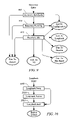
- FIG. 1 is an illustrative block diagram of a system 100 in accordance with one embodiment of the present invention.
- system 100 includes two components 105 and 110 that are communicatively coupled by a data bus 115 comprised of a plurality of serial data lanes 120 and bus interfaces 130 and 135 .
- bus 115 is part of a system in which a first component 105 is an end-point device, such as a graphical processing unit (GPU).
- the other component 110 may correspond to a bridge, such as a root complex for peripheral devices.
- a CPU 170 and memory 180 having executable software instructions 190 may be coupled to component 110 .
- bus 115 may be utilized in a variety of systems other than that illustrated in FIG. 1 .
- each of the serial data lanes 120 corresponds to a pair of serial simplex data links to transmit and receive data.
- each serial simplex data link may correspond to a high-speed differential pair with a transmitter disposed in one bus interface and a corresponding receiver in the other bus interface, with the high-speed differential pair having a data rate and associated data bandwidth.
- Each serial simplex data link may transmit an embedded data clock. A logical idle may be transmitted on the data lanes even when no data is being transmitted.
- Each bus interface 130 and 135 includes its own local link state machine 140 for initializing a common data link between the components in which one or more of the data lanes are associated to form a common data link.
- N active serial data lanes where N is an integer
- the link between the components is a “by N link” having N active lanes.
- the bandwidth of the link scales with the number of active lanes that are associated to form the link between the components.
- a transmission code such as 8 bit/10 bit encoding, may be used to send serial data symbols on each data lane that represent bytes of a larger word of data transmitted on the bus, i.e., the word of data is encoded for transmission on one or more lanes of the bus.
- the bandwidth of the bus scales with the number of active lanes. Consequently, a by N link has a bandwidth proportional to its link width, where the link width is the integer number of active data lanes that are associated to form the common data link between the components. (The link width is also commonly referred to as the “bus width.”) Additionally, since only the active lanes (i.e., powered lanes with embedded clocks) consume significant power, the power consumption of the bus also scales proportionally with the number of active lanes used in the link.
- At least one of the bus interfaces includes an adaptive link width controller 150 .
- Adaptive link width controller 150 acts to adjust the integer number of active lanes in accordance with changes in bandwidth requirements for the bus, i.e., it selects a subset of operable data lanes to be used to transmit/receive data, where the subset is in the range of 1 to K lanes, where K is the maximum integer number of operable data lanes supported by the interfaces. This permits the link width to be adapted to be a minimum number sufficient to provide the required bandwidth, thereby reducing the power consumption of the bus during time periods when a low bandwidth is sufficient while permitting the bus bandwidth to be increased during time periods when a high bandwidth is required.
- the bus determines 205 operable serial data lanes and operating parameters for the data lanes.
- the interfaces of the bus negotiate 210 an integer number, M (M ⁇ K), of active data lanes for an operational linkwidth.
- M integer number
- the bus may then enter a normal operational state in which data may be exchanged across the bus using the M active data lanes.
- the interfaces of the bus In response to a condition for which the bus bandwidth requirements change, the interfaces of the bus re-negotiate 215 the number of active data lanes used in the link to a different integer number, N, corresponding to a different link width (i.e., M ⁇ N, N ⁇ K).
- the bus may then enter a normal operational state in which data is exchanged across the bus using the N data lanes. The process may continue based on other conditions. For example, another condition may occur which triggers the interfaces of the bus to renegotiate 220 the number of active data lanes used in the link to a third integer number, L, of active data lanes.
- a computing system may have bus bandwidth requirements corresponding to two or more levels of bus traffic, such as low and high bandwidth requirements or high, medium, and low bandwidth requirements.
- the bandwidth requirements may be associated with the type of software being executed by system 100 .
- word processing applications commonly have comparatively low bandwidth requirements in comparison to high-performance three-dimensional graphics applications.
- the bandwidth requirements of a software application may be detected from an attribute of the software.
- some software applications, such as high-performance graphics applications include function or resource calls that are indicative of their bandwidth requirements.
- some system states may be detected by hardware, such as idle states or busy “wait states” in which a portion of system 100 may be internally processing information such that the system generates comparatively little traffic for bus 115 .
- power management software may reduce bus bandwidth in a low power mode and increase bus bandwidth for an active mode.
- adaptive link width controller 150 includes link width control registers 160 that may be written into by hardware or software detection elements (not shown in FIG. 1 ) when an event is detected corresponding to a change in the bandwidth requirements for bus 115 .
- the bus interfaces 130 and 135 form the link between the components through a training sequence in which training sequence signals are sent back and forth between the bus interfaces to communicate information and coordinate the states of each interface.
- the training sequence messages permit one of the interfaces to trigger the other interface to enter a different state of its link state machine 140 .
- a first link width may be negotiated whereas a second link width may be subsequently negotiated using a second training sequence.
- a first bus interface receives 305 a signal enabling re-negotiation of link width and which places a constraint on the bus link width.
- the first bus interfaces exits the normal operational state (sometimes known as “L0”) and generates 310 one or more training sequences selected to trigger itself and the second bus interface to enter a configuration state.
- the first bus interface imposes 315 a constraint on the number of operable data lanes that may be used. This may, for example, include creating training sequence messages that indicate to the other interface that certain lanes are not to be used, even though they are operable lanes (e.g., by sending a signal indicating that one or more lanes are disabled).
- the bus completes configuration 320 and returns to the normal operational state with the modified bus lane width.
- one interface control the renegotiation process, i.e., both trigger the initial re-negotiation and also place a constraint on the lane width during the negotiation.
- one interface may trigger the re-negotiation process while the other interface places the constraint on the lane width during the re-negotiation.
- Each re-negotiation process is significantly faster that the initial negotiation because one or more steps used in the initial link initialization process may be omitted in the renegotiation process.
- a conventional bus reset or power up operation includes resetting the state of registers, detecting operable data lanes, and setting common communication parameters of the lanes. This corresponds to Reset, Detect, and Polling states used in an initialization process.
- the Reset, Detect, and Polling states require a substantial amount of time in comparison to the configuration state used to negotiate link width. Consequently, in the present invention each re-negotiation can be fast in comparison to a reset process.
- FIG. 4 is a state diagram for link state machine 140 in one embodiment of the present invention.
- the link is initialized by triggering a reset state 405 .
- a detect state 410 is entered to detect operable lanes.
- a Polling state 415 is entered to poll the lanes and arrive at common operating parameters such that the lanes may communicate training sequences.
- a configuration state 420 is entered to configure the link.
- the configuration state 420 includes link width negotiation. After the link is configured, the bus enters an operational state 425 in which the bus is capable of transmitting data.
- additional low power operational modes may be entered from operational state 425 .
- additional low power operational modes e.g., L1 and L2 sleep states for the entire link width
- L1 and L2 sleep states for the entire link width
- the renegotiation process uses one or more additional states of the link state machine to access the configuration state 420 from operational state 425 .
- a recovery state 430 is sometimes included in a link state machine to permit a bus to recover an attribute of the bus.
- the renegotiation process begins in the normal operational state 425 .
- One of the interfaces generates a training sequence that causes both interfaces to enter recovery state 430 .
- From recovery state 430 the interfaces then enter configuration state 420 and re-negotiate link width using any constraints on link width imposed by the initiating user interface.
- FIG. 5 illustrates a state machine diagram for an alternate embodiment.
- the initiating interface generates training messages that cause a transition to the Recovery state 430 .
- the state machines From the recovery state 430 the state machines enter a Loopback state 435 .
- Loopback states are sometimes included in bus interfaces to perform diagnostics of individual components.
- the Detect state 410 is entered from the Loopback state 435 .
- the Reset state 405 is avoided.
- the interactions of the state machines may be adapted to eliminate some of the sub-states of the detect state.
- bus 115 is compliant with the Peripheral Component Interconnect (PCI) ExpressTM standard and a PCI express implementation will now be described.
- PCI ExpressTM is a standard developed by the PCI-SIG industry organization. The protocols of the PCI ExpressTM specification are described in the “PCI ExpressTM Base Specification,” version 1(a), available from the PCI-SIG organization via the World Wide Web at the URL address: www.pcisig.com, the contents of which are hereby incorporated by reference.
- each point-to-point link between components may have 1, 2, 4, 8, 12, 16, or 32 dual simplex 2.5 Gbps lanes.
- PCI ExpressTM calls for 8 bit/10 bit data encoding to create a 2 differential pair, 2.5 Gbps (2.0 Gbps effective rate) dual simplex data stream with an embedded clock.
- a “symbol” is the 10 bit quantity produced as a result of 8b/10b encoding.
- the PCI ExpressTM specification calls for the link width to be negotiated to the maximum link width supported by both sides of the bus.
- link state machine 140 executes the states of the link training and status state machine (LTSSM) of the PCI ExpressTM specification.
- LTSSM link training and status state machine
- the PCI ExpressTM specification specifies mandatory LTSSM states and training set protocols. However, the PCI ExpressTM specification also permits individual developers to implement optional modifications as long as they are compatible with mandatory states and mandatory protocols. In the PCI ExpressTM protocol, training sequences are commonly denoted as TS1 or TS2 training sets.
- downstream refers to a relative position that is farther away from a root complex and a downstream request is one in which information is flowing away from root complex (e.g., towards an endpoint device).
- upstream refers to a relative position that is closer to the root complex and upstream request is one in which information is flowing towards the root complex (e.g., from an endpoint device).
- the signal that triggers a link width renegotiation may be received by a re-negotiation control register(s) within the link width control registers 160 .
- a signal from hardware or software indicative of a change in bus bandwidth requirements may be used to generate an enable signal and maximum lane width written into re-negotiation control registers (RNCTRL).
- the maximum lane width estimate should be compliant with a supported integer number of lane widths.
- re-negotiation control register includes an enable bit, RNCTRL.Enable to enable re-negotiation and a maximum width bus field RNCTRL.Maxwidth to indicate the maximum number of lanes required.
- training sequences are in the form of ordered sets TS1 and TS2 for initializing bit alignment, symbol alignment, and to negotiate physical layer parameters for operation, such as the link identification number and the lane ordering within the link.
- Control bits are included in TS1 and TS2 to perform specific functions.
- the TS1 and TS2 training sequences are used to discover and determine link width, link data rate, lane reversal, and polarity inversion.
- Training also includes link data rate negotiation, bit lock per lane, lane polarity, symbol lock per lane, lane ordering within a link, link width negotiation, and lane-to-lane deskew.
- the PCI ExpressTM protocol uses TS1 training ordered-sets to provide proposals or counter-proposals of certain physical layer operational parameters and uses TS2 training ordered-sets to accept the proposals and confirm the parameters.
- PCI ExpressTM also includes special symbols that are distinct from data symbols. These include special symbols used for link management.
- the symbol “PAD” is used in framing and link width and lane ordering negotiations.
- the LTSSM of each interface of a PCI ExpressTM implementation includes a Reset state 405 , Detect state 410 , Polling state 415 , Configuration state 420 , Normal Operational state 425 , Recovery state 430 , and Loopback state 435 . Details of these states specific to practicing a PCI ExpressTM embodiment will now be described.
- FIG. 6 is a block diagram illustrating a detect sub-state machine for implementing a detect state of a PCI ExpressTM LTSSM.
- a detect state the transmitter performs a receiver detection sequence on unconfigured lanes that can form one or more links.
- a Detect.Quiet state 605 is entered if a receiver is not detected on any lanes. If a receiver is detected on all active lanes, the Detect.Active state 610 is entered. If the Detect.Active state 610 succeeds in detecting receivers on all active lanes then the detect state exits to polling 615 .
- a re-association process is initiated in the LTSSM for unconfigured lanes that did not detect a receiver.
- the PCI ExpressTM specification defines a protocol of training sets for each detect sub-state.
- FIG. 7 is a block diagram illustrating a polling sub-state machine for implementing a polling state of a PCI ExpressTM LTSSM.
- the polling state training ordered sets are sent and received.
- bit lock is established, symbol lock is established, lane polarity is established, and lane data rate is established.
- the polling sub-states correspond to a Polling.Active state 705 that sends out TS1 ordered sets to indicate that polling is active and to establish bit and symbol lock, a Polling.Compliance state 710 for use with test equipment to assess if the bus is compliant with voltage and timing specifications, a Polling.Configuration state 715 sending out TS2 training ordered sets to confirm bit lock, symbol lock, and data rate, and to invert the polarity, if necessary, and a Polling.Speed state 720 to change the data rate to the highest data rate supported on both sides of the bus.
- the PCI ExpressTM specification defines a protocol of training sets for each polling sub-state.
- FIG. 8 is a block diagram illustrating a configuration sub-state machine for implementing a configuration state of a PCI ExpressTM implementation.
- the lanes are configured into a link through a link width and lane ordering negotiation sequence.
- the PCI ExpressTM specification includes the configuration sub-states of Configuration.Linkwidth.start 805 to initiate a link width negotiation by proposing a link identification number on the desired active lanes of the link, Configuration.Linkwidth.Accept 810 to accept the link identification number and to counter-propose the number of desired active lanes, Configuration.Lanenum.Wait 815 for proposing and counter-proposing the desired lane ordering, Configuration.Lanenum.Accept 820 for accepting lane ordering assignments, Configuration.Complete 825 to confirm completion of configuration, and Configuration.Idle 830 to place the link in a logically idle condition prior to the normal operational state.
- the PCI ExpressTM specification defines a protocol of training sets for each configuration sub-state.
- FIG. 9 is a block diagram illustrating a sub-state machine for implementing a recovery state of a PCI ExpressTM LTSSM.
- the recovery state allows a configured link to re-establish bit lock, symbol lock, and lane-to-lane de-skew.
- the transmitter and receivers are sending and receiving data using the configured link and lane number as well as the previously negotiated data rate.
- the recovery sub-state machine includes a Recovery.Rcvrlock state 905 that sends ordered training sets to re-establish bit and symbol lock, a Recovery.RcvrCfg state 910 to re-establish lane-to-lane deskew and re-confirm the lane ordering assignment, and a Recovery.Idle state 915 that permits access to other states, based upon directions or other conditions.
- the PCI ExpressTM specification defines a protocol of training sets for each recovery sub-state.
- FIG. 10 is a block diagram illustrating the sub-states of loopback specified in PCI ExpressTM for the LTSSM.
- Loopback state 450 is conventionally included to allow for component testing and fault isolation. During loopback data that is sent out is looped back to test data paths of the bus. These include a Loopback.Entry state 1005 to enter loopback, a Loopback.Active state 1010 for an active loopback mode, and a Loopback.Exit state 1015 for a condition exiting loopback.
- the PCI ExpressTM specification defines a protocol of training sets for each loopback sub-state.
- the two LTSSMs of the bus interfaces interact through TS1 and TS2 ordered training sets that are exchanged between the LTSSMs.
- the interactions between the LTSSMs cause them to move through a sequence of sub-states.
- at least one of the LTSSMs is adapted to create training sequences that initiate the link width renegotiation process and that places a constraint on the link width negotiation.
- the PAD symbol is inserted in training sequences to disable selected lanes.
- FIGS. 11A and 11B are a flow chart illustrating a PCI ExpressTM implementation in which an end point device initiates the renegotiation process by triggering entry into the recovery state to enter the configuration state to renegotiate lane widths.
- Steps 1105 – 1140 illustrate a reduction of link width whereas steps 1145 – 1170 outline the steps for an increase in link width (which are illustrated in FIGS. 12A–13B in more detail).
- a hardware or software entity activates re-negotiation in the endpoint device. This includes asserting 1105 the RNCTRL.Enable bit and writing the RNCTRL.Maxwidth field of the renegotiation control register(s).
- the interface compares 1110 RNCTRL.Maxwidth to the value of the LinkStat.Linkwidth, the currently negotiated bus width recorded in a link status register. If LinkState.Linkwidth, M, is greater than RNCTRL.Maxwidth, N, (e.g., N ⁇ M), it corresponds to a determination that the bus width can be reduced to save power.
- the endpoint device LTSSM then enters 1115 the recovery state. It sends out training sets TS1 and TS2 according to the current link and lane numbers as specified by the PCI ExpressTM for the Recovery.Rcvrlock and Recovery.Rcvrcfg states of the recovery sub-state machine.
- the upstream device e.g., the root complex
- the upstream device is driven 1120 into the recovery state upon detecting the TS1/TS2 training sets sent by the downstream device.
- the link number and lane number fields in the TS1/TS2 remain the same as for previously negotiated values during Recovery.Rcvrlock and Recovery.Rcvrcfg. Since the link number and lane number fields are unchanged, the Recover.RcvrLock and Recovery.RcvrCfg sub-states may be completed comparatively quickly, e.g., around 32 TS1/TS2 periods, or 512 Symbol times. This results in both ends of the link being driven into the Recovery.Idle sub-state at the end of recovery.
- the endpoint device sends out 1125 TS1 ordered sets on all configured lanes with the link number the same as the original value.
- the lane number field of the TS1 ordered sets is assigned the value of “PAD”.
- the endpoint device enters the configuration sub-state Configuration.Linkwidth.Start.
- the upstream component is driven 1130 into the configuration state by receiving TS1 ordered sets with lane number being “PAD”.
- TS1 ordered sets with lane number field being “PAD” on the Recovery.Idle state causes the upstream component to enter the Configuration.Linkwidth.Start sub-state.
- link width re-negotiation begins.
- the endpoint device uses the RNCTRL.MAXWIDTH setting to disable 1135 a selected number of the originally enabled lanes such that the total number of enabled lanes at the endpoint component is no greater than RNCTRL.Maxwidth.
- the normal operation state is entered 1140 with the new bus width of RNCTRL.Maxwidth.
- link width which corresponds to RNCTRL.Maxwidth being greater than the current negotiated link width (N>M).
- the route depends whether the current negotiated link width is less than the maximum link width (K) (e.g., the maximum that would be negotiated without a RNCTR.Maxwidth constraint, which is obtained during the initial power-up negotiation process) and upon whether the upstream device is adapted to support renegotiation by entering the configuration state directly from the recovery state.
- K maximum link width
- the condition N>M and M ⁇ K is evaluated 1145 to see if further increase in link width is possible. If no further increase in link width is permitted, a return 1160 is made to the operational state with the bandwidth unchanged (since it is already at a maximum). If the link width can be increased, a determination is made whether the upstream device supports 1150 a fast bus width re-negotiation protocol that enters 1155 the configuration state directly from the recovery state. If the upstream device does not support a fast bus width renegotiation protocol, a protocol is used 1170 which enters the configuration state through the loopback state.
- FIG. 12 illustrates an embodiment in which fast renegotiation of an increase in bus width is not supported by the upstream device.
- a determination that the upstream devices does not support fast renegotiation can be made 1205 , for example, by examining a vendor ID field to determine the functionality of the upstream device.
- the endpoint device LTSSM enters 1210 the recovery state and sends out TSI/TS2 training sets according to the current link and lane numbers during the Recovery.RcvrLock and Recovery.RcvrCfg sub-states. Additionally, the loopback bit in the training control field of the TS1/TS2 training sets is asserted.
- the upstream device In response to the TS1/TS2 ordered sets, the upstream device is driven 1220 into the Recovery state. Consequently, both ends of the link are driven into the Recovery.Idle sub-state of the recovery state after Recovery.RcvrLock and Recovery.RcvrCfg.
- the endpoint device sends out 1230 TS1 ordered sets on all configured lanes with the loopback bit in the training control field asserted.
- the endpoint device LTSSM enters the Loopback.Entry sub-state of the loopback state as the loopback master.
- the upstream component is driven 1240 into the Loopback.Active sub-state as a loopback slave after receiving TS1 with loopback asserted while it is in the Recovery.Idle state.
- the upstream component then starts looping back the TS1 ordered sets with the loopback bit asserted that are received from the endpoint component.
- the endpoint component can then exit 1260 the loopback state.
- the endpoint component enters the Polling.Active sub-state with all K lanes that are maximally configured without a RNCTR.Maxwidth constraint.
- the (K–M) lanes which are enabled at the initial power-up negotiation process but are disabled for power reduction, are re-activated here to start the link-width increase negotiation process.
- the upstream component exits 1270 the Loopback.Exit sub-state and enters the Detect.Quiet sub-state.
- the upstream component will be driven into the Polling state with K active lanes as well.
- the re-negotiation begins with the maximum number of active lanes negotiated during the initial power-up negotiation. For a maximum number of lanes, K, and a RNCTRL.Maxwidth value of N, the endpoint device selects the minimum of N and K as the new lane width, and use the information to constrain the re-negotiation process.
- lanes that are selected to be disabled send 1280 pad symbols in the link and lane numbers fields of TS1/TS2 ordered sets. In this way, the bus exits 1290 to the normal operating state at the end of configuration with a new link width no greater than RNCTRL.Maxwidth.
- FIGS. 13A and 13B are a flowchart illustrating a bus width upgrade protocol that is supported by the upstream device.
- a determination that the upstream device supports 1305 fast renegotiation may be made, for example, using a vendor ID field of a training set.
- the endpoint device enters 1310 the Recovery.RcvrLock sub-state.
- the M currently configured lanes send out TS1 training sets according to the current link and lane numbers.
- the previously disabled (K–M) lanes among the K maximally negotiated lanes are re-activated.
- the PAD symbol is sent in the link number and lane number fields of TS1 training sets, and their receivers have to perform bit and symbol lock as well during the Recovery.RcvrCfg state.
- the next state, Recover.RcvrCfg, for the endpoint device is not reached until all of the K lanes achieve bit and symbol lock.
- the upstream device is driven 1320 into the Recovery.RcvrLock state upon detecting TS1 ordered sets from the endpoint device on the M currently configured lanes. Once an electrical idle exit is detected on the formerly disabled (K–M) lanes, the lanes are re-activated and start sending TS1 ordered sets with link and lane number fields set to PAD. The next state Recover.RcvrCfg is not entered until all K lanes achieve bit and symbol lock.
- the endpoint device sends out 1340 TS1 ordered sets with link and lane number fields set to PAD on all K enabled lanes (including M currently configured and (K–M) re-activated lanes).
- the endpoint device LTSSM enters the configuration sub-state Configuration.Linkwidth.Start.
- the upstream component After receiving a TS1 ordered set with the lane numbers set to PAD, the upstream component is driven 1350 into the Configuration state and begins the lane width re-negotiation with K active lanes.
- the re-negotiation begins with the maximum number of active lanes negotiated during the initial power-up negotiation. For a maximum number of lanes, K, and a RNCTRL.Maxwidth value of N, the endpoint selects the minimum of N and K as the new link width, and uses the information to constrain the re-negotiation process.
- lanes that are to be disabled send 1360 pad symbols in the link and lane numbers fields of TS1/TS2 ordered sets. In this way, the bus then exits 1370 to the normal operating state at the end of configuration with a new link width no greater than RNCTRL.Maxwidth.
- One application of the present invention is in a computer system having a CPU, GPU, and software applications with different bus bandwidth needs.
- some high performance graphics applications e.g., three-dimensional graphics applications
- a GPU executing a high performance graphics applications requires substantial computing power.
- the bus of the present invention preferably is part of a larger power saving architecture in which the GPU and the bus have power-saving modes that permit both GPU power and bus power to be decreased when high performance graphics applications are not in use.
- FIG. 14 is a flow chart of one method of saving power in a graphics system. Responsive to detecting an idle state for the system, 3-D graphics may be disabled 1410 . This may include, for example, switching a GPU to a low-power consumption state.
- the bus is configured to have a minimum link width 1420 (e.g., one lane).
- the bus is configured 1440 to have a link width appropriate for the application.
- the GPU is configured 1450 for the need of the application.
- a bus having 16 active lanes may be required.
- the power consumption may be 100 milliwatts per active lane per direction, or 200 milliwatts per lane.
- the link width may be negotiated to a low number for other applications, e.g., one lane for a text processing application.
- Negotiating a 1 lane configuration when high bus bandwidth is not required results in a savings of 3 Watts, or 94% of the bus power.
- the present invention permits the bus width to be negotiated in a comparatively short time.
- completion of the detect and polling states takes at least 12 milliseconds.
- the configuration state takes only a few microseconds to complete. Consequently, the present invention permits a comparatively fast renegotiation.
- the renegotiation process may be sufficiently rapid that it does not interfere with a user's experience.
- An embodiment of the present invention relates to a computer storage product with a computer-readable medium having computer code thereon for performing various computer-implemented operations.
- the media and computer code may be those specially designed and constructed for the purposes of the present invention, or they may be of the kind well known and available to those having skill in the computer software arts.
- Examples of computer-readable media include, but are not limited to: magnetic media such as hard disks, floppy disks, and magnetic tape; optical media such as CD-ROMs and holographic devices; magneto-optical media such as floptical disks; and hardware devices that are specially configured to store and execute program code, such as application-specific integrated circuits (“ASICs”), programmable logic devices (“PLDs”) and ROM and RAM devices.
- ASICs application-specific integrated circuits
- PLDs programmable logic devices
- Examples of computer code include machine code, such as produced by a compiler, and files containing higher-level code that are executed by a computer using an interpreter.
- machine code such as produced by a compiler
- files containing higher-level code that are executed by a computer using an interpreter.
- an embodiment of the invention may be implemented using Java, C++, or other object-oriented programming language and development tools.
- Another embodiment of the invention may be implemented in hardwired circuitry in place of, or in combination with, machine-executable software instructions.
Abstract
A bus permits the number of active serial data lanes of a data link to be re-negotiated in response to changes in bus bandwidth requirements. In one embodiment, one of the bus interfaces triggers a re-negotiation of link width and places a constraint on link width during the re-negotiation.
Description
The present invention is generally related to bus power optimization for a bus comprised of a plurality of serial data lanes. More particularly, the present invention is directed towards optimizing bus power in peripheral component interfaces.
There is an increasing need to reduce the power consumption of personal computers and other types of computing devices. A high-power consumption is undesirable because it increases the cooling requirements of the personal computer. Additionally, a high-power consumption is undesirable because it reduces the battery lifetime of mobile computers.
There are several components of a personal computer that draw significant amounts of power. First, the chip containing the central processing unit (CPU) draws power. Second, other chips, such as a graphics processing unit (GPU) or a bridge chipset, also consume power.
Additionally, a high-performance personal computer requires high-bandwidth data buses to transfer data between components. High-bandwidth data buses also consume a significant amount of power. The power required to operate a high-bandwidth data bus can be significant, particularly in the context of a mobile personal computer having a limited power budget.
Therefore, what is desired is an apparatus, system, and method for reducing bus power for a high bandwidth data bus.
An apparatus, system, and method is disclosed in which a data bus has a plurality of operable data lanes that may be associated to form a data link between components. The data bus permits the number of active data lanes of the data link to be adaptively adjusted in response to changes in bus bandwidth requirements. The bus is configured to have a sufficient number of active lanes to provide a high bandwidth for operational states requiring high bandwidth. However, for operational states requiring less bandwidth, the bus is configured to have a smaller number of active lanes sufficient to supply the reduced bandwidth requirement of the operational state, reducing the bus power requirements.
In one embodiment of a method of the present invention, in a first operational state having a first link bandwidth requirement, a first link width is negotiated having a first integer number, M, of active data lanes, where M is less than or equal to a maximum integer number, K, of operable data lanes. In response to detecting a second operational state having a second link bandwidth requirement, a second link width is negotiated having a second integer number, N, of active data lanes, where N is not equal to M, and N is also less than or equal to K.
In one embodiment of a bus of the present invention, the bus includes a first data interface, a second data interface, and a plurality of data lanes for communicating data between the first data interface and the second data interface. The first and second data interfaces are adapted to initiate a negotiation for a number of active data lanes corresponding to a subset of operable data lanes. The first and second data interfaces also re-negotiate the number of active data lanes to place a constraint on the number of active data lanes associated to form the link in response to a re-negotiation signal.
In one embodiment of a computing system of the present invention comprises a root complex, a CPU coupled to the root complex for executing a software application stored in a memory, an endpoint device associating a graphical processing unit, and a bus having a plurality of data lanes coupling the root complex to the endpoint device. The bus is configured to associate data lanes into a common link having a link width corresponding to a number of active data lanes selected to adapt to the bandwidth requirements of the graphical processing unit.
The invention is more fully appreciated in connection with the following detailed description taken in conjunction with the accompanying drawings, in which:
Like reference numerals refer to corresponding parts throughout the several views of the drawings.
The present invention is directed towards an apparatus, system, and method for adaptively adjusting bus bandwidth. FIG. 1 is an illustrative block diagram of a system 100 in accordance with one embodiment of the present invention. Referring to FIG. 1 , system 100 includes two components 105 and 110 that are communicatively coupled by a data bus 115 comprised of a plurality of serial data lanes 120 and bus interfaces 130 and 135.
In some embodiments, bus 115 is part of a system in which a first component 105 is an end-point device, such as a graphical processing unit (GPU). The other component 110 may correspond to a bridge, such as a root complex for peripheral devices. A CPU 170 and memory 180 having executable software instructions 190 may be coupled to component 110. However, it will be understood in the following description that bus 115 may be utilized in a variety of systems other than that illustrated in FIG. 1 .
In one embodiment, each of the serial data lanes 120 corresponds to a pair of serial simplex data links to transmit and receive data. For example, each serial simplex data link may correspond to a high-speed differential pair with a transmitter disposed in one bus interface and a corresponding receiver in the other bus interface, with the high-speed differential pair having a data rate and associated data bandwidth. Each serial simplex data link may transmit an embedded data clock. A logical idle may be transmitted on the data lanes even when no data is being transmitted.
Each bus interface 130 and 135 includes its own local link state machine 140 for initializing a common data link between the components in which one or more of the data lanes are associated to form a common data link. With N active serial data lanes, where N is an integer, the link between the components is a “by N link” having N active lanes. The bandwidth of the link scales with the number of active lanes that are associated to form the link between the components. In particular, a transmission code, such as 8 bit/10 bit encoding, may be used to send serial data symbols on each data lane that represent bytes of a larger word of data transmitted on the bus, i.e., the word of data is encoded for transmission on one or more lanes of the bus.
Assuming that each data lane transmits data at the same rate, the bandwidth of the bus scales with the number of active lanes. Consequently, a by N link has a bandwidth proportional to its link width, where the link width is the integer number of active data lanes that are associated to form the common data link between the components. (The link width is also commonly referred to as the “bus width.”) Additionally, since only the active lanes (i.e., powered lanes with embedded clocks) consume significant power, the power consumption of the bus also scales proportionally with the number of active lanes used in the link.
At least one of the bus interfaces includes an adaptive link width controller 150. Adaptive link width controller 150 acts to adjust the integer number of active lanes in accordance with changes in bandwidth requirements for the bus, i.e., it selects a subset of operable data lanes to be used to transmit/receive data, where the subset is in the range of 1 to K lanes, where K is the maximum integer number of operable data lanes supported by the interfaces. This permits the link width to be adapted to be a minimum number sufficient to provide the required bandwidth, thereby reducing the power consumption of the bus during time periods when a low bandwidth is sufficient while permitting the bus bandwidth to be increased during time periods when a high bandwidth is required.
Referring to the flowchart of FIG. 2 , in one embodiment the bus determines 205 operable serial data lanes and operating parameters for the data lanes. As an illustrative example, there may be a maximum integer number, K, of operable data lanes that are supported by both interfaces, where K is ≧2. At a certain point of time, the interfaces of the bus negotiate 210 an integer number, M (M≦K), of active data lanes for an operational linkwidth. The bus may then enter a normal operational state in which data may be exchanged across the bus using the M active data lanes. In response to a condition for which the bus bandwidth requirements change, the interfaces of the bus re-negotiate 215 the number of active data lanes used in the link to a different integer number, N, corresponding to a different link width (i.e., M≠N, N≦K). The bus may then enter a normal operational state in which data is exchanged across the bus using the N data lanes. The process may continue based on other conditions. For example, another condition may occur which triggers the interfaces of the bus to renegotiate 220 the number of active data lanes used in the link to a third integer number, L, of active data lanes.
For example, a computing system may have bus bandwidth requirements corresponding to two or more levels of bus traffic, such as low and high bandwidth requirements or high, medium, and low bandwidth requirements. The bandwidth requirements may be associated with the type of software being executed by system 100. For example, word processing applications commonly have comparatively low bandwidth requirements in comparison to high-performance three-dimensional graphics applications. The bandwidth requirements of a software application may be detected from an attribute of the software. For example, some software applications, such as high-performance graphics applications, include function or resource calls that are indicative of their bandwidth requirements. Additionally, some system states may be detected by hardware, such as idle states or busy “wait states” in which a portion of system 100 may be internally processing information such that the system generates comparatively little traffic for bus 115. Moreover, in one embodiment, power management software may reduce bus bandwidth in a low power mode and increase bus bandwidth for an active mode.
In one embodiment, adaptive link width controller 150 includes link width control registers 160 that may be written into by hardware or software detection elements (not shown in FIG. 1 ) when an event is detected corresponding to a change in the bandwidth requirements for bus 115.
In one embodiment, the bus interfaces 130 and 135 form the link between the components through a training sequence in which training sequence signals are sent back and forth between the bus interfaces to communicate information and coordinate the states of each interface. Among other tasks, the training sequence messages permit one of the interfaces to trigger the other interface to enter a different state of its link state machine 140. Thus, in a first training sequence a first link width may be negotiated whereas a second link width may be subsequently negotiated using a second training sequence.
Referring to the flowchart of FIG. 3 , in one embodiment a first bus interface receives 305 a signal enabling re-negotiation of link width and which places a constraint on the bus link width. The first bus interfaces exits the normal operational state (sometimes known as “L0”) and generates 310 one or more training sequences selected to trigger itself and the second bus interface to enter a configuration state. In the configuration state, the first bus interface imposes 315 a constraint on the number of operable data lanes that may be used. This may, for example, include creating training sequence messages that indicate to the other interface that certain lanes are not to be used, even though they are operable lanes (e.g., by sending a signal indicating that one or more lanes are disabled). The bus completes configuration 320 and returns to the normal operational state with the modified bus lane width.
It is preferable to have one interface control the renegotiation process, i.e., both trigger the initial re-negotiation and also place a constraint on the lane width during the negotiation. However, it will be understood that in alternative embodiments one interface may trigger the re-negotiation process while the other interface places the constraint on the lane width during the re-negotiation.
Each re-negotiation process is significantly faster that the initial negotiation because one or more steps used in the initial link initialization process may be omitted in the renegotiation process. For example, a conventional bus reset or power up operation includes resetting the state of registers, detecting operable data lanes, and setting common communication parameters of the lanes. This corresponds to Reset, Detect, and Polling states used in an initialization process. The Reset, Detect, and Polling states require a substantial amount of time in comparison to the configuration state used to negotiate link width. Consequently, in the present invention each re-negotiation can be fast in comparison to a reset process.
Referring to arrows 480 and 485, the renegotiation process uses one or more additional states of the link state machine to access the configuration state 420 from operational state 425. A recovery state 430 is sometimes included in a link state machine to permit a bus to recover an attribute of the bus. In one embodiment, the renegotiation process begins in the normal operational state 425. One of the interfaces generates a training sequence that causes both interfaces to enter recovery state 430. From recovery state 430 the interfaces then enter configuration state 420 and re-negotiate link width using any constraints on link width imposed by the initiating user interface.
The apparatus, system, and method of the present invention may be adapted for use in a variety of bus types and bus protocols. In one embodiment, bus 115 is compliant with the Peripheral Component Interconnect (PCI) Express™ standard and a PCI express implementation will now be described. PCI Express™ is a standard developed by the PCI-SIG industry organization. The protocols of the PCI Express™ specification are described in the “PCI Express™ Base Specification,” version 1(a), available from the PCI-SIG organization via the World Wide Web at the URL address: www.pcisig.com, the contents of which are hereby incorporated by reference.
In the PCI Express™ specification each point-to-point link between components may have 1, 2, 4, 8, 12, 16, or 32 dual simplex 2.5 Gbps lanes. PCI Express™ calls for 8 bit/10 bit data encoding to create a 2 differential pair, 2.5 Gbps (2.0 Gbps effective rate) dual simplex data stream with an embedded clock. In PCI Express™, a “symbol” is the 10 bit quantity produced as a result of 8b/10b encoding. The PCI Express™ specification calls for the link width to be negotiated to the maximum link width supported by both sides of the bus.
In a PCI Express™ implementation, link state machine 140 executes the states of the link training and status state machine (LTSSM) of the PCI Express™ specification. The PCI Express™ specification specifies mandatory LTSSM states and training set protocols. However, the PCI Express™ specification also permits individual developers to implement optional modifications as long as they are compatible with mandatory states and mandatory protocols. In the PCI Express™ protocol, training sequences are commonly denoted as TS1 or TS2 training sets.
In a PCI Express™ implementation the term “downstream” refers to a relative position that is farther away from a root complex and a downstream request is one in which information is flowing away from root complex (e.g., towards an endpoint device). Conversely, in a PCI Express™ implementation the term “upstream” refers to a relative position that is closer to the root complex and upstream request is one in which information is flowing towards the root complex (e.g., from an endpoint device).
Referring back to FIG. 1 , in one embodiment of a PCI Express™ implementation the signal that triggers a link width renegotiation may be received by a re-negotiation control register(s) within the link width control registers 160. For example, a signal from hardware or software indicative of a change in bus bandwidth requirements may be used to generate an enable signal and maximum lane width written into re-negotiation control registers (RNCTRL). The maximum lane width estimate should be compliant with a supported integer number of lane widths. In one implementation, re-negotiation control register includes an enable bit, RNCTRL.Enable to enable re-negotiation and a maximum width bus field RNCTRL.Maxwidth to indicate the maximum number of lanes required.
In PCI Express™, training sequences are in the form of ordered sets TS1 and TS2 for initializing bit alignment, symbol alignment, and to negotiate physical layer parameters for operation, such as the link identification number and the lane ordering within the link. Control bits are included in TS1 and TS2 to perform specific functions. The TS1 and TS2 training sequences are used to discover and determine link width, link data rate, lane reversal, and polarity inversion. Training also includes link data rate negotiation, bit lock per lane, lane polarity, symbol lock per lane, lane ordering within a link, link width negotiation, and lane-to-lane deskew. In general, the PCI Express™ protocol uses TS1 training ordered-sets to provide proposals or counter-proposals of certain physical layer operational parameters and uses TS2 training ordered-sets to accept the proposals and confirm the parameters.
PCI Express™ also includes special symbols that are distinct from data symbols. These include special symbols used for link management. The symbol “PAD” is used in framing and link width and lane ordering negotiations.
Referring again to FIGS. 4 and 5 , the LTSSM of each interface of a PCI Express™ implementation includes a Reset state 405, Detect state 410, Polling state 415, Configuration state 420, Normal Operational state 425, Recovery state 430, and Loopback state 435. Details of these states specific to practicing a PCI Express™ embodiment will now be described.
In a PCI Express™ implementation, the two LTSSMs of the bus interfaces interact through TS1 and TS2 ordered training sets that are exchanged between the LTSSMs. The interactions between the LTSSMs cause them to move through a sequence of sub-states. In the present invention, at least one of the LTSSMs is adapted to create training sequences that initiate the link width renegotiation process and that places a constraint on the link width negotiation. As described below in more detail, in one embodiment the PAD symbol is inserted in training sequences to disable selected lanes.
Referring to FIGS. 11A and 11B , in one embodiment a hardware or software entity activates re-negotiation in the endpoint device. This includes asserting 1105 the RNCTRL.Enable bit and writing the RNCTRL.Maxwidth field of the renegotiation control register(s).
The interface compares 1110 RNCTRL.Maxwidth to the value of the LinkStat.Linkwidth, the currently negotiated bus width recorded in a link status register. If LinkState.Linkwidth, M, is greater than RNCTRL.Maxwidth, N, (e.g., N<M), it corresponds to a determination that the bus width can be reduced to save power. The endpoint device LTSSM then enters 1115 the recovery state. It sends out training sets TS1 and TS2 according to the current link and lane numbers as specified by the PCI Express™ for the Recovery.Rcvrlock and Recovery.Rcvrcfg states of the recovery sub-state machine.
As a result the upstream device (e.g., the root complex) is driven 1120 into the recovery state upon detecting the TS1/TS2 training sets sent by the downstream device. The link number and lane number fields in the TS1/TS2 remain the same as for previously negotiated values during Recovery.Rcvrlock and Recovery.Rcvrcfg. Since the link number and lane number fields are unchanged, the Recover.RcvrLock and Recovery.RcvrCfg sub-states may be completed comparatively quickly, e.g., around 32 TS1/TS2 periods, or 512 Symbol times. This results in both ends of the link being driven into the Recovery.Idle sub-state at the end of recovery.
At the recovery.idle sub-state, instead of placing the link into a locally idle state by sending null symbols, the endpoint device sends out 1125 TS1 ordered sets on all configured lanes with the link number the same as the original value. The lane number field of the TS1 ordered sets is assigned the value of “PAD”. The endpoint device enters the configuration sub-state Configuration.Linkwidth.Start.
The upstream component is driven 1130 into the configuration state by receiving TS1 ordered sets with lane number being “PAD”. In one embodiment, two consecutive TS1 ordered sets with lane number field being “PAD” on the Recovery.Idle state causes the upstream component to enter the Configuration.Linkwidth.Start sub-state.
With both components in the Configuration.Linkwidt.Start sub-state, link width re-negotiation begins. During re-negotiation, the endpoint device uses the RNCTRL.MAXWIDTH setting to disable 1135 a selected number of the originally enabled lanes such that the total number of enabled lanes at the endpoint component is no greater than RNCTRL.Maxwidth. As a result, the normal operation state is entered 1140 with the new bus width of RNCTRL.Maxwidth.
Referring to comparison step 1110, it is also necessary to negotiate increases in link width, which corresponds to RNCTRL.Maxwidth being greater than the current negotiated link width (N>M). The route depends whether the current negotiated link width is less than the maximum link width (K) (e.g., the maximum that would be negotiated without a RNCTR.Maxwidth constraint, which is obtained during the initial power-up negotiation process) and upon whether the upstream device is adapted to support renegotiation by entering the configuration state directly from the recovery state.
The condition N>M and M<K is evaluated 1145 to see if further increase in link width is possible. If no further increase in link width is permitted, a return 1160 is made to the operational state with the bandwidth unchanged (since it is already at a maximum). If the link width can be increased, a determination is made whether the upstream device supports 1150 a fast bus width re-negotiation protocol that enters 1155 the configuration state directly from the recovery state. If the upstream device does not support a fast bus width renegotiation protocol, a protocol is used 1170 which enters the configuration state through the loopback state.
Negotiating an increase in link width depends upon whether the upstream device (e.g., the root complex) obeys the standard PCI Express™ protocol or has been modified to support a fast renegotiation. This is due, in part, to the nature of the specific mandatory protocols of the PCI Express™ specification. For the case that the upstream device does not support fast renegotiation, the entry to the configuration step may require entry via the loopback step, as illustrated in FIG. 5 . However, if the upstream device supports fast negotiation, the entry to the configuration may be made directly from the configuration step, as illustrated in FIG. 4 .
In response to the TS1/TS2 ordered sets, the upstream device is driven 1220 into the Recovery state. Consequently, both ends of the link are driven into the Recovery.Idle sub-state of the recovery state after Recovery.RcvrLock and Recovery.RcvrCfg.
At the Recovery.Idle sub-state, the endpoint device sends out 1230 TS1 ordered sets on all configured lanes with the loopback bit in the training control field asserted. The endpoint device LTSSM enters the Loopback.Entry sub-state of the loopback state as the loopback master.
The upstream component is driven 1240 into the Loopback.Active sub-state as a loopback slave after receiving TS1 with loopback asserted while it is in the Recovery.Idle state. The upstream component then starts looping back the TS1 ordered sets with the loopback bit asserted that are received from the endpoint component.
In response to the endpoint component receiving the TS1 looped back from the upstream device, it skips the Loopback.Active state and enters 1250 Loopback.Exit immediately. This drives the upstream device into the Loopback.Exit state as well.
The endpoint component can then exit 1260 the loopback state. In one embodiment, the endpoint component enters the Polling.Active sub-state with all K lanes that are maximally configured without a RNCTR.Maxwidth constraint. The (K–M) lanes, which are enabled at the initial power-up negotiation process but are disabled for power reduction, are re-activated here to start the link-width increase negotiation process.
The upstream component exits 1270 the Loopback.Exit sub-state and enters the Detect.Quiet sub-state. In response to the K active lanes in the endpoint component, the upstream component will be driven into the Polling state with K active lanes as well.
Note that by re-activating the disabled lanes in the endpoint component, the re-negotiation begins with the maximum number of active lanes negotiated during the initial power-up negotiation. For a maximum number of lanes, K, and a RNCTRL.Maxwidth value of N, the endpoint device selects the minimum of N and K as the new lane width, and use the information to constrain the re-negotiation process. During configuration, lanes that are selected to be disabled send 1280 pad symbols in the link and lane numbers fields of TS1/TS2 ordered sets. In this way, the bus exits 1290 to the normal operating state at the end of configuration with a new link width no greater than RNCTRL.Maxwidth.
The endpoint device enters 1310 the Recovery.RcvrLock sub-state. The M currently configured lanes send out TS1 training sets according to the current link and lane numbers. The previously disabled (K–M) lanes among the K maximally negotiated lanes are re-activated. For the re-activated lanes, the PAD symbol is sent in the link number and lane number fields of TS1 training sets, and their receivers have to perform bit and symbol lock as well during the Recovery.RcvrCfg state. The next state, Recover.RcvrCfg, for the endpoint device is not reached until all of the K lanes achieve bit and symbol lock.
The upstream device is driven 1320 into the Recovery.RcvrLock state upon detecting TS1 ordered sets from the endpoint device on the M currently configured lanes. Once an electrical idle exit is detected on the formerly disabled (K–M) lanes, the lanes are re-activated and start sending TS1 ordered sets with link and lane number fields set to PAD. The next state Recover.RcvrCfg is not entered until all K lanes achieve bit and symbol lock.
At the Recovery.RcvrCfg sub-state, all of the M currently configured lanes send out 1330 and detect TS2 ordered sets. The (K–M) re-activated lanes also send TS1 or TS2 ordered sets in order to keep the bit and symbol lock on the other side of the link. Both ends of the link then enter the Recovery.Idle sub-state.
At the Recovery.Idle sub-state, the endpoint device sends out 1340 TS1 ordered sets with link and lane number fields set to PAD on all K enabled lanes (including M currently configured and (K–M) re-activated lanes). The endpoint device LTSSM enters the configuration sub-state Configuration.Linkwidth.Start.
After receiving a TS1 ordered set with the lane numbers set to PAD, the upstream component is driven 1350 into the Configuration state and begins the lane width re-negotiation with K active lanes.
Note that by re-activating the disabled lanes in both components, the re-negotiation begins with the maximum number of active lanes negotiated during the initial power-up negotiation. For a maximum number of lanes, K, and a RNCTRL.Maxwidth value of N, the endpoint selects the minimum of N and K as the new link width, and uses the information to constrain the re-negotiation process. During Configuration sub-states, lanes that are to be disabled send 1360 pad symbols in the link and lane numbers fields of TS1/TS2 ordered sets. In this way, the bus then exits 1370 to the normal operating state at the end of configuration with a new link width no greater than RNCTRL.Maxwidth.
One application of the present invention is in a computer system having a CPU, GPU, and software applications with different bus bandwidth needs. In particular, some high performance graphics applications (e.g., three-dimensional graphics applications) have extremely high bandwidth requirements in comparison to other applications, such as text processing or two-dimensional graphics. Additionally, a GPU executing a high performance graphics applications requires substantial computing power. In a graphics system the bus of the present invention preferably is part of a larger power saving architecture in which the GPU and the bus have power-saving modes that permit both GPU power and bus power to be decreased when high performance graphics applications are not in use.
Some of the benefits of the present invention will now be discussed with regards to an exemplary implementation. In a high performance graphics system, a bus having 16 active lanes may be required. For the operational (L0) state, the power consumption may be 100 milliwatts per active lane per direction, or 200 milliwatts per lane. Thus, in 16 lane configuration a PCI Express™ bus may consume 3.2 Watts of power. However, in the present invention, the link width may be negotiated to a low number for other applications, e.g., one lane for a text processing application. Negotiating a 1 lane configuration when high bus bandwidth is not required results in a savings of 3 Watts, or 94% of the bus power.
Additionally, the present invention permits the bus width to be negotiated in a comparatively short time. In a PCI Express implementation, completion of the detect and polling states takes at least 12 milliseconds. By comparison, the configuration state takes only a few microseconds to complete. Consequently, the present invention permits a comparatively fast renegotiation. In the context of a graphics system, the renegotiation process may be sufficiently rapid that it does not interfere with a user's experience.
An embodiment of the present invention relates to a computer storage product with a computer-readable medium having computer code thereon for performing various computer-implemented operations. The media and computer code may be those specially designed and constructed for the purposes of the present invention, or they may be of the kind well known and available to those having skill in the computer software arts. Examples of computer-readable media include, but are not limited to: magnetic media such as hard disks, floppy disks, and magnetic tape; optical media such as CD-ROMs and holographic devices; magneto-optical media such as floptical disks; and hardware devices that are specially configured to store and execute program code, such as application-specific integrated circuits (“ASICs”), programmable logic devices (“PLDs”) and ROM and RAM devices. Examples of computer code include machine code, such as produced by a compiler, and files containing higher-level code that are executed by a computer using an interpreter. For example, an embodiment of the invention may be implemented using Java, C++, or other object-oriented programming language and development tools. Another embodiment of the invention may be implemented in hardwired circuitry in place of, or in combination with, machine-executable software instructions.
The foregoing description, for purposes of explanation, used specific nomenclature to provide a thorough understanding of the invention. However, it will be apparent to one skilled in the art that specific details are not required in order to practice the invention. Thus, the foregoing descriptions of specific embodiments of the invention are presented for purposes of illustration and description. They are not intended to be exhaustive or to limit the invention to the precise forms disclosed; obviously, many modifications and variations are possible in view of the above teachings. The embodiments were chosen and described in order to best explain the principles of the invention and its practical applications, they thereby enable others skilled in the art to best utilize the invention and various embodiments with various modifications as are suited to the particular use contemplated. It is intended that the following claims and their equivalents define the scope of the invention.
Claims (23)
1. A method of bus power management, comprising:
for a first operational state having a first link bandwidth requirement for a bus, negotiating a first link width between a first bus interface and a second bus interface disposed at opposite ends of said bus based on said first link bandwidth requirement, said first link width having a first integer number, M, of active data lanes that is less than or equal to a maximum integer number, K, of operable data lanes; and
in response to detecting a second operational state having a second link bandwidth requirement, negotiating a second link width between said first bus interface and said second bus interface based on said second link bandwidth requirement said second link width having a second integer number, N, of active data lanes, where N is not equal to M, and N is also less than or equal to K;
wherein the number of active data lanes that is negotiated is based on a bandwidth constraint to reduce the power consumption associated with active data lanes.
2. The method of claim 1 , wherein said negotiating said first link width comprises:
selecting M=K.
3. The method of claim 2 , wherein negotiating said second link width comprises:
selecting N to be a minimum number sufficient to provide the bandwidth required for said second operational state.
4. The method of claim 1 , further comprising: prior to negotiating said first link width, detecting operable data lanes and establishing common communication parameters on said lanes.
5. The method of claim 4 , further comprising: storing initialization data describing operable data lanes and their communication parameters for subsequent negotiations.
6. The method of claim 1 , wherein said second operational state is associated with a change in a type of software application being executed.
7. The method of claim 1 , wherein said second operational state is associated with a change in a state of operation of a central processing unit.
8. The method of claim 7 , wherein said state of operation of said central processing unit is selected from the group consisting of a busy state, an idle state, and a run state.
9. The method of claim 1 , wherein said negotiating said second link width comprises: generating a disable signal to disable operable data lanes to reduce link bandwidth.
10. The method of claim 1 , wherein said negotiating said second link width comprises: enabling previously disabled operable data lanes to increase link bandwidth.
11. The method of claim 1 , wherein negotiating said second link width further comprises:
a first component triggering entry of a second component into a recovery state;
said first component further generating training sets during said recovery state to trigger said first component and said second component to enter a configuration state in which lane widths are negotiated for said bus.
12. The method of claim 11 , wherein said first component generates training sets in said configuration state that selectively disable a subset of operable data lanes.
13. The method of claim 1 , wherein negotiating said second link width further comprises:
a first component triggering entry of a second component into a recovery state;
said first component further generating training sets during said recovery state to initiate said second component to enter a loopback state;
said first component generating training sets during loopback to initiate said second component to enter a detect state, from which a configuration state is entered in which lane width is negotiated;
wherein re-negotiation of lane widths occurs without a reset phase.
14. A method of bus power management:
detecting operable data lanes in a detect state;
establishing common communication parameters for said data lanes in a subsequent polling state;
entering a configuration state;
for a first operational state having a first link bandwidth requirement, negotiating a first link width between a first bus interface at one end of a bus and a second bus interface at another end of the bus, said first link width having a first integer number, M, of active data lanes that is less than or equal to a maximum integer number, K, of operable data lanes;
entering an operational state with said first integer number, M, of active data lanes associated as a link between bus components;
triggering entry back into said configuration state in response to detecting a second operational state having a second link bandwidth requirement;
negotiating a second link width between said first bus interface and said second bus interface, said second link width having a second integer number, N, of active data lanes, where N is not equal to M, and N is also less than or equal to K;
and entering said second operational state with said second integer number, N, of active data lanes associated as said link between said bus components
wherein the number of active data lanes that is negotiated is based on a bandwidth constraint to reduce the power consumption associated with active data lanes.
15. The method of claim 14 , wherein triggering entry back into said configuration state comprises:
in response to detecting said second operational state, entering a recovery state; and
from said recovery state, entering said configuration state.
16. The method of claim 14 , wherein triggering entry back into said configuration state further comprises:
in response to detecting said second operational state, entering a recovery state; and
from said recovery state, entering a loopback state;
from said loopback state, re-entering said detect state;
wherein a reset state is avoided.
17. A data bus, comprising:
a first data interface disposed at one end of said data bus;
a second data interface disposed at the other end of said data bus;
a plurality of data lanes for communicating data between said first data interface and said second data interface;
said first data interface and said second data interface adapted to initiate a negotiation for a number of active lanes corresponding to a subset of operable data lanes;
said first data interface and said second data interface re-negotiating the number of active data lanes to place a constraint on the number of active data lanes associated to form a link in response to a re-negotiation signal;
wherein the number of active data lanes that is negotiated is based on a bandwidth constraint to reduce the power consumption associated with active data lanes.
18. The bus of claim 17 , wherein said first and second interfaces are PCI Express™ compliant.
19. The bus of claim 17 , wherein one of said interfaces selectively disables a number of operable data lanes to adjust bandwidth.
20. The bus of claim 17 , wherein one of the interfaces selectively enables a number of operable data lanes to adjust bandwidth.
21. A computing system, comprising:
a root complex;
a CPU coupled to the root complex for executing a software application stored in a memory;
an endpoint device associating a graphical processing unit (GPU);
a bus having a plurality of data lanes coupling the root complex to the endpoint device;
the bus having bus interface disposed at two ends of the bus configured to associate active data lanes into a common link having a lane width corresponding to a number of active data lanes selected to adapt to the bandwidth requirements of the GPU;
wherein the number of active data lanes that is negotiated is based on a bandwidth constraint to reduce the power consumption associated with active data lanes.
22. The computing system of claim 21 , wherein the bus includes bus interfaces disposed in the root complex and the endpoint device, wherein the interfaces are configured to re-negotiate a lane width of the bus in response to a re-negotiation signal.
23. The computing system of claim 21 , wherein the bus retains detect and polling information from an initial set-up procedure for use during subsequent lane width negotiations.
Priority Applications (5)
| Application Number | Priority Date | Filing Date | Title |
|---|---|---|---|
| US10/431,994 US7136953B1 (en) | 2003-05-07 | 2003-05-07 | Apparatus, system, and method for bus link width optimization |
| US11/229,208 US7426597B1 (en) | 2003-05-07 | 2005-09-16 | Apparatus, system, and method for bus link width optimization of a graphics system |
| US11/281,718 US7370132B1 (en) | 2003-05-07 | 2005-11-16 | Logical-to-physical lane assignment to reduce clock power dissipation in a bus having a variable link width |
| US11/613,150 US7469311B1 (en) | 2003-05-07 | 2006-12-19 | Asymmetrical bus |
| US12/252,525 US7788439B1 (en) | 2003-05-07 | 2008-10-16 | Asymmetrical bus for bus link width optimization of a graphics system |
Applications Claiming Priority (1)
| Application Number | Priority Date | Filing Date | Title |
|---|---|---|---|
| US10/431,994 US7136953B1 (en) | 2003-05-07 | 2003-05-07 | Apparatus, system, and method for bus link width optimization |
Related Child Applications (1)
| Application Number | Title | Priority Date | Filing Date |
|---|---|---|---|
| US11/229,208 Continuation-In-Part US7426597B1 (en) | 2003-05-07 | 2005-09-16 | Apparatus, system, and method for bus link width optimization of a graphics system |
Publications (1)
| Publication Number | Publication Date |
|---|---|
| US7136953B1 true US7136953B1 (en) | 2006-11-14 |
Family
ID=37397788
Family Applications (2)
| Application Number | Title | Priority Date | Filing Date |
|---|---|---|---|
| US10/431,994 Active 2024-12-18 US7136953B1 (en) | 2003-05-07 | 2003-05-07 | Apparatus, system, and method for bus link width optimization |
| US11/281,718 Expired - Fee Related US7370132B1 (en) | 2003-05-07 | 2005-11-16 | Logical-to-physical lane assignment to reduce clock power dissipation in a bus having a variable link width |
Family Applications After (1)
| Application Number | Title | Priority Date | Filing Date |
|---|---|---|---|
| US11/281,718 Expired - Fee Related US7370132B1 (en) | 2003-05-07 | 2005-11-16 | Logical-to-physical lane assignment to reduce clock power dissipation in a bus having a variable link width |
Country Status (1)
| Country | Link |
|---|---|
| US (2) | US7136953B1 (en) |
Cited By (135)
| Publication number | Priority date | Publication date | Assignee | Title |
|---|---|---|---|---|
| US20050027900A1 (en) * | 2003-04-18 | 2005-02-03 | Nextio Inc. | Method and apparatus for a shared I/O serial ATA controller |
| US20050083954A1 (en) * | 2003-08-16 | 2005-04-21 | Phoenix Contact Gmbh & Co. Kg | Method and apparatus for the transmission of data via a bus network using the broadcast principle |
| US20050228932A1 (en) * | 2004-04-09 | 2005-10-13 | Asrock Incorporation | Computer system with a PCI express interface |
| US20050256984A1 (en) * | 2004-05-13 | 2005-11-17 | Jenkins Peter J | Implementation of a master loopback mode |
| US20050262284A1 (en) * | 2004-05-21 | 2005-11-24 | Naveen Cherukuri | Method for identifying bad lanes and exchanging width capabilities of two CSI agents connected across a link |
| US20050268137A1 (en) * | 2003-01-21 | 2005-12-01 | Nextio Inc. | Method and apparatus for a shared I/O network interface controller |
| US20050270988A1 (en) * | 2004-06-04 | 2005-12-08 | Dehaemer Eric | Mechanism of dynamic upstream port selection in a PCI express switch |
| US20060023633A1 (en) * | 2004-07-16 | 2006-02-02 | Ati Technologies Inc. | Method and apparatus for managing power consumption relating to a differential serial communication link |
| US20060034295A1 (en) * | 2004-05-21 | 2006-02-16 | Intel Corporation | Dynamically modulating link width |
| US20060200598A1 (en) * | 2004-04-08 | 2006-09-07 | Janzen Jeffery W | System and method for optimizing interconnections of components in a multichip memory module |
| US20060282602A1 (en) * | 2005-06-09 | 2006-12-14 | Tse-Hsine Liao | Data transmission device and method thereof |
| US20060285847A1 (en) * | 2005-06-17 | 2006-12-21 | Intel Corporation | Systems with variable link widths |
| US20070008898A1 (en) * | 2005-06-29 | 2007-01-11 | Intel Corporation | Point-to-point link negotiation method and apparatus |
| US20070025354A1 (en) * | 2003-01-21 | 2007-02-01 | Nextio Inc. | Method and apparatus for shared i/o in a load/store fabric |
| US20070041405A1 (en) * | 2005-06-23 | 2007-02-22 | Navada Muraleedhara H | Method and system for response determinism by synchronization |
| US20070067548A1 (en) * | 2005-08-19 | 2007-03-22 | Juenger Randall E | System and method for dynamic adjustment of an information handling system graphics bus |
| US20070079047A1 (en) * | 2005-09-28 | 2007-04-05 | Ati Technologies Inc. | Lane merging |
| US20070088894A1 (en) * | 2004-02-04 | 2007-04-19 | Hofmann Richard G | Scalable Bus Structure |
| US20070094437A1 (en) * | 2005-10-26 | 2007-04-26 | Jabori Monji G | Dynamic lane management system and method |
| US20070130407A1 (en) * | 2005-11-22 | 2007-06-07 | Olson David M | Bus system with multiple modes of operation |
| US20070150762A1 (en) * | 2005-12-28 | 2007-06-28 | Sharma Debendra D | Using asymmetric lanes dynamically in a multi-lane serial link |
| US20070233930A1 (en) * | 2006-03-14 | 2007-10-04 | International Business Machines Corporation | System and method of resizing PCI Express bus widths on-demand |
| US20070239925A1 (en) * | 2006-04-11 | 2007-10-11 | Nec Corporation | PCI express link, multi host computer system, and method of reconfiguring PCI express link |
| US20070239922A1 (en) * | 2005-12-09 | 2007-10-11 | Horigan John W | Technique for link reconfiguration |
| US20070276981A1 (en) * | 2006-05-24 | 2007-11-29 | Atherton William E | Dynamically Allocating Lanes to a Plurality of PCI Express Connectors |
| US20080022024A1 (en) * | 2006-07-20 | 2008-01-24 | Jin-Liang Mao | Method for link bandwidth management |
| US20080028126A1 (en) * | 2006-07-26 | 2008-01-31 | Gerald Keith Bartley | Memory System Having an Apportionable Data Bus and Daisy Chained Memory Chips |
| US20080028175A1 (en) * | 2006-07-26 | 2008-01-31 | Gerald Keith Bartley | Self Timed Memory Chip Having an Apportionable Data Bus |
| US20080028125A1 (en) * | 2006-07-26 | 2008-01-31 | Gerald Keith Bartley | Computer System Having an Apportionable Data Bus |
| US20080040529A1 (en) * | 2006-07-26 | 2008-02-14 | Gerald Keith Bartley | Memory Chip Having an Apportionable Data Bus |
| US7366864B2 (en) * | 2004-03-08 | 2008-04-29 | Micron Technology, Inc. | Memory hub architecture having programmable lane widths |
| US20080228981A1 (en) * | 2006-05-24 | 2008-09-18 | Atherton William E | Design structure for dynamically allocating lanes to a plurality of pci express connectors |
| US20080263246A1 (en) * | 2007-04-17 | 2008-10-23 | Larson Chad J | System and Method for Balancing PCI-Express Bandwidth |
| US20080263254A1 (en) * | 2007-04-20 | 2008-10-23 | Via Technologies, Inc. | Method and System For Adjusting Bus Frequency And Link Width On A Bus |
| US20080288798A1 (en) * | 2007-05-14 | 2008-11-20 | Barnes Cooper | Power management of low power link states |
| US20080298383A1 (en) * | 2007-06-01 | 2008-12-04 | James Wang | Buffer Minimization in Interface Controller |
| US20090043931A1 (en) * | 2004-03-19 | 2009-02-12 | Koninklijke Philips Electronics, N.V. | Automatic configuration of a communication port as transmitter or receiver depending on the sensed transfer direction of a connected device |
| US20090094401A1 (en) * | 2007-10-03 | 2009-04-09 | Larson Chad J | System for Dynamically Balancing PCI-Express Bandwidth |
| US20090103444A1 (en) * | 2007-10-22 | 2009-04-23 | Dell Products L.P. | Method and Apparatus for Power Throttling of Highspeed Multi-Lane Serial Links |
| US20090103443A1 (en) * | 2007-10-22 | 2009-04-23 | Ting Sheng Ku | Loopback configuration for bi-directional interfaces |
| US20090119532A1 (en) * | 2007-11-06 | 2009-05-07 | Russell Newcomb | Method and system for a free running strobe tolerant interface |
| US20090157920A1 (en) * | 2007-12-13 | 2009-06-18 | International Business Machines Corporation | Dynamically Allocating Communication Lanes For A Plurality Of Input/Output ('I/O') Adapter Sockets In A Point-To-Point, Serial I/O Expansion Subsystem Of A Computing System |
| US20090164684A1 (en) * | 2007-12-20 | 2009-06-25 | International Business Machines Corporation | Throttling A Point-To-Point, Serial Input/Output Expansion Subsystem Within A Computing System |
| US20090187683A1 (en) * | 2008-01-22 | 2009-07-23 | International Business Machines Corporation | Adaptive link width control |
| US20090228626A1 (en) * | 2008-03-07 | 2009-09-10 | Via Technologies, Inc. | Host modules, electronic devices, electronic systems and data transmission method thereof |
| US7617333B2 (en) | 2003-01-21 | 2009-11-10 | Nextio Inc. | Fibre channel controller shareable by a plurality of operating system domains within a load-store architecture |
| US7620064B2 (en) | 2003-01-21 | 2009-11-17 | Nextio Inc. | Method and apparatus for shared I/O in a load/store fabric |
| US20090307437A1 (en) * | 2003-03-13 | 2009-12-10 | Marvell World Trade Ltd. | Multiport Memory Architecture, Devices and Systems Including the Same, and Methods of Using the Same |
| US7639627B1 (en) * | 2005-02-18 | 2009-12-29 | Sprint Communications Company L.P. | System and method for trace replay using parallelized streams |
| US20090327536A1 (en) * | 2008-06-30 | 2009-12-31 | Gary Solomon | Asymmetrical universal serial bus communications |
| US7698489B1 (en) * | 2008-02-04 | 2010-04-13 | Nvidia Corporation | Method for dynamically turning off bus signals into a GPU |
| US7698483B2 (en) | 2003-01-21 | 2010-04-13 | Nextio, Inc. | Switching apparatus and method for link initialization in a shared I/O environment |
| US7746095B2 (en) | 2003-06-11 | 2010-06-29 | Round Rock Research, Llc | Memory module and method having improved signal routing topology |
| US7788439B1 (en) | 2003-05-07 | 2010-08-31 | Nvidia Corporation | Asymmetrical bus for bus link width optimization of a graphics system |
| US7793029B1 (en) | 2005-05-17 | 2010-09-07 | Nvidia Corporation | Translation device apparatus for configuring printed circuit board connectors |
| US7805586B2 (en) | 2002-08-29 | 2010-09-28 | Micron Technology, Inc. | System and method for optimizing interconnections of memory devices in a multichip module |
| US7836211B2 (en) | 2003-01-21 | 2010-11-16 | Emulex Design And Manufacturing Corporation | Shared input/output load-store architecture |
| US7899969B2 (en) | 2004-03-25 | 2011-03-01 | Round Rock Research, Llc | System and method for memory hub-based expansion bus |
| US7917658B2 (en) | 2003-01-21 | 2011-03-29 | Emulex Design And Manufacturing Corporation | Switching apparatus and method for link initialization in a shared I/O environment |
| US7949817B1 (en) * | 2007-07-31 | 2011-05-24 | Marvell International Ltd. | Adaptive bus profiler |
| US7949803B2 (en) | 2004-08-31 | 2011-05-24 | Micron Technology, Inc. | System and method for transmitting data packets in a computer system having a memory hub architecture |
| US7953074B2 (en) | 2003-01-21 | 2011-05-31 | Emulex Design And Manufacturing Corporation | Apparatus and method for port polarity initialization in a shared I/O device |
| US20110128963A1 (en) * | 2009-11-30 | 2011-06-02 | Nvidia Corproation | System and method for virtual channel communication |
| CN101609442B (en) * | 2009-06-17 | 2011-06-08 | 成都市华为赛门铁克科技有限公司 | Interface self-adapting method, device and system thereof |
| US20110173352A1 (en) * | 2010-01-13 | 2011-07-14 | Mellanox Technologies Ltd | Power Reduction on Idle Communication Lanes |
| US7983181B1 (en) * | 2006-03-28 | 2011-07-19 | Advanced Micro Devices, Inc. | Technique for negotiating a width of a packet-based communication link |
| US8021193B1 (en) | 2005-04-25 | 2011-09-20 | Nvidia Corporation | Controlled impedance display adapter |
| US8102843B2 (en) * | 2003-01-21 | 2012-01-24 | Emulex Design And Manufacturing Corporation | Switching apparatus and method for providing shared I/O within a load-store fabric |
| US8234425B1 (en) | 2007-06-27 | 2012-07-31 | Marvell International Ltd. | Arbiter module |
| US8346884B2 (en) | 2003-01-21 | 2013-01-01 | Nextio Inc. | Method and apparatus for a shared I/O network interface controller |
| US20130067127A1 (en) * | 2011-08-24 | 2013-03-14 | Nvidia Corporation | Method and apparatus for interleaving bursts of high-speed serial interconnect link training with bus data transactions |
| US8412872B1 (en) | 2005-12-12 | 2013-04-02 | Nvidia Corporation | Configurable GPU and method for graphics processing using a configurable GPU |
| US8417838B2 (en) | 2005-12-12 | 2013-04-09 | Nvidia Corporation | System and method for configurable digital communication |
| US20130159589A1 (en) * | 2010-08-19 | 2013-06-20 | Fujitsu Limited | Bus control device and bus control method |
| EP2642480A1 (en) * | 2010-11-19 | 2013-09-25 | Sharp Kabushiki Kaisha | Data forwarding circuit, data forwarding method, display device, host-side device, and electronic apparatus |
| US8589643B2 (en) | 2003-10-20 | 2013-11-19 | Round Rock Research, Llc | Arbitration system and method for memory responses in a hub-based memory system |
| US20130346653A1 (en) * | 2012-06-20 | 2013-12-26 | International Business Machines Corporation | Versatile lane configuration using a pcie pie-8 interface |
| US20140019654A1 (en) * | 2011-12-21 | 2014-01-16 | Malay Trivedi | Dynamic link width adjustment |
| US8683085B1 (en) | 2008-05-06 | 2014-03-25 | Marvell International Ltd. | USB interface configurable for host or device mode |
| US8687639B2 (en) | 2009-06-04 | 2014-04-01 | Nvidia Corporation | Method and system for ordering posted packets and non-posted packets transfer |
| US8688922B1 (en) | 2010-03-11 | 2014-04-01 | Marvell International Ltd | Hardware-supported memory management |
| US8704275B2 (en) | 2004-09-15 | 2014-04-22 | Nvidia Corporation | Semiconductor die micro electro-mechanical switch management method |
| US8711156B1 (en) | 2004-09-30 | 2014-04-29 | Nvidia Corporation | Method and system for remapping processing elements in a pipeline of a graphics processing unit |
| US8711161B1 (en) | 2003-12-18 | 2014-04-29 | Nvidia Corporation | Functional component compensation reconfiguration system and method |
| US8732644B1 (en) | 2003-09-15 | 2014-05-20 | Nvidia Corporation | Micro electro mechanical switch system and method for testing and configuring semiconductor functional circuits |
| US8768642B2 (en) | 2003-09-15 | 2014-07-01 | Nvidia Corporation | System and method for remotely configuring semiconductor functional circuits |
| US8775997B2 (en) | 2003-09-15 | 2014-07-08 | Nvidia Corporation | System and method for testing and configuring semiconductor functional circuits |
| US8819326B1 (en) * | 2006-12-12 | 2014-08-26 | Spansion Llc | Host/client system having a scalable serial bus interface |
| US20140244904A1 (en) * | 2013-02-28 | 2014-08-28 | Kabushiki Kaisha Toshiba | Memory device and computer system |
| US8843723B1 (en) | 2010-07-07 | 2014-09-23 | Marvell International Ltd. | Multi-dimension memory timing tuner |
| US8868955B2 (en) | 2011-07-01 | 2014-10-21 | Intel Corporation | Enhanced interconnect link width modulation for power savings |
| US8874833B1 (en) | 2009-03-23 | 2014-10-28 | Marvell International Ltd. | Sequential writes to flash memory |
| US8904077B1 (en) * | 2007-06-26 | 2014-12-02 | Qlogic, Corporation | Power management for host bus adapters |
| US20150156007A1 (en) * | 2013-11-29 | 2015-06-04 | Huawei Technologies Co., Ltd. | Link adjusting method and apparatus |
| US9053244B2 (en) | 2012-06-28 | 2015-06-09 | Intel Corporation | Utilization-aware low-overhead link-width modulation for power reduction in interconnects |
| US9070454B1 (en) | 2009-04-21 | 2015-06-30 | Marvell International Ltd. | Flash memory |
| US9070451B1 (en) | 2008-04-11 | 2015-06-30 | Marvell International Ltd. | Modifying data stored in a multiple-write flash memory cell |
| US20150212755A1 (en) * | 2014-01-30 | 2015-07-30 | Avalanche Technology, Inc. | Method of managing throughput of redundant array of independent disks (raid) groups in a solid state disk array |
| US9176909B2 (en) * | 2009-12-11 | 2015-11-03 | Nvidia Corporation | Aggregating unoccupied PCI-e links to provide greater bandwidth |
| US9183171B2 (en) | 2012-09-29 | 2015-11-10 | Intel Corporation | Fast deskew when exiting low-power partial-width high speed link state |
| US9223735B2 (en) | 2012-05-22 | 2015-12-29 | Intel Corporation | Providing a consolidated sideband communication channel between devices |
| US9262360B2 (en) * | 2012-06-29 | 2016-02-16 | Intel Corporation | Architected protocol for changing link operating mode |
| US20160050301A1 (en) * | 2014-08-18 | 2016-02-18 | International Business Machines Corporation | System interconnect dynamic scaling handshake using spare bit-lane |
| US20160062943A1 (en) * | 2014-08-28 | 2016-03-03 | Fujitsu Limited | Apparatus and method for controlling the number of lanes used for transferring data between information processing apparatuses |
| US9331869B2 (en) | 2010-03-04 | 2016-05-03 | Nvidia Corporation | Input/output request packet handling techniques by a device specific kernel mode driver |
| US9330031B2 (en) | 2011-12-09 | 2016-05-03 | Nvidia Corporation | System and method for calibration of serial links using a serial-to-parallel loopback |
| US9390046B2 (en) | 2012-06-27 | 2016-07-12 | Intel Corporation | Controlling a physical link of a first protocol using an extended capability structure of a second protocol |
| US9423864B2 (en) | 2011-07-27 | 2016-08-23 | Huawei Technologies Co., Ltd. | PCI express device and link energy management method and device |
| US9524013B2 (en) | 2014-04-16 | 2016-12-20 | International Business Machines Corporation | System interconnect dynamic scaling by lane width and operating frequency balancing |
| US9552045B2 (en) | 2014-03-20 | 2017-01-24 | Intel Corporation | Method, apparatus, and system for controlling power consumption of unused hardware of a link interface |
| US9569188B1 (en) * | 2015-08-04 | 2017-02-14 | International Business Machines Corporation | Compiling source code to reduce run-time execution of vector element reverse operations |
| US9606780B2 (en) | 2014-12-19 | 2017-03-28 | International Business Machines Corporation | Compiler method for generating instructions for vector operations on a multi-endian processor |
| US9619214B2 (en) | 2014-08-13 | 2017-04-11 | International Business Machines Corporation | Compiler optimizations for vector instructions |
| WO2017165657A1 (en) * | 2016-03-23 | 2017-09-28 | Qualcomm Incorporated | Link speed control systems for power optimization |
| US9847891B2 (en) | 2011-08-24 | 2017-12-19 | Nvidia Corporation | System and method for detecting reuse of an existing known high-speed serial interconnect link |
| US9880821B2 (en) | 2015-08-17 | 2018-01-30 | International Business Machines Corporation | Compiler optimizations for vector operations that are reformatting-resistant |
| CN107918594A (en) * | 2016-10-05 | 2018-04-17 | 三星电子株式会社 | Semiconductor device, the method for operating semiconductor device and the system including the device |
| US10169014B2 (en) | 2014-12-19 | 2019-01-01 | International Business Machines Corporation | Compiler method for generating instructions for vector operations in a multi-endian instruction set |
| US20190064915A1 (en) * | 2016-06-30 | 2019-02-28 | Intel IP Corporation | Interprocessor power state transitions |
| US20190081900A1 (en) * | 2018-11-13 | 2019-03-14 | Intel Corporation | System, Apparatus And Method For Traffic Shaping Of Data Communication Via An Interconnect |
| US10412673B2 (en) | 2017-05-28 | 2019-09-10 | Mellanox Technologies Tlv Ltd. | Power-efficient activation of multi-lane ports in a network element |
| US20190286605A1 (en) * | 2019-06-07 | 2019-09-19 | Intel Corporation | Data structures for refined link training |
| US10521391B1 (en) * | 2018-11-29 | 2019-12-31 | Apple Inc. | Chip to chip interface with scalable bandwidth |
| US20200226084A1 (en) * | 2019-11-27 | 2020-07-16 | Intel Corporation | Partial link width states for bidirectional multilane links |
| EP3706008A1 (en) * | 2019-03-05 | 2020-09-09 | INTEL Corporation | Partial link width states for multilane links |
| US10817043B2 (en) * | 2011-07-26 | 2020-10-27 | Nvidia Corporation | System and method for entering and exiting sleep mode in a graphics subsystem |
| US11073894B2 (en) | 2019-05-24 | 2021-07-27 | Qualcomm Incorporated | System power management for peripheral component interconnect express (PCIE)-based devices |
| US11157068B2 (en) * | 2019-01-25 | 2021-10-26 | Intel Corporation | Power state management for lanes of a communication port |
| US11188494B2 (en) | 2019-05-21 | 2021-11-30 | Google Llc | Asymmetric data communication for host-device interface |
| US11239843B2 (en) | 2018-05-30 | 2022-02-01 | Intel Corporation | Width and frequency conversion with PHY layer devices in PCI-express |
| US20220075752A1 (en) * | 2018-04-16 | 2022-03-10 | Intel Corporation | Precoding mechanism in pci-express |
| WO2022156778A1 (en) * | 2021-01-25 | 2022-07-28 | 华为技术有限公司 | Method and apparatus for adjusting link width |
| CN115098427A (en) * | 2022-06-24 | 2022-09-23 | 中国电子科技集团公司第五十八研究所 | Method for realizing link width self-adaption |
| US11467999B2 (en) | 2018-06-29 | 2022-10-11 | Intel Corporation | Negotiating asymmetric link widths dynamically in a multi-lane link |
| DE112013007752B3 (en) | 2012-10-22 | 2023-04-27 | Intel Corporation | High performance wiring physical layer |
Families Citing this family (28)
| Publication number | Priority date | Publication date | Assignee | Title |
|---|---|---|---|---|
| US20060280202A1 (en) * | 2005-06-13 | 2006-12-14 | Analog Devices, Inc. | MEMS sensor with configuration module |
| US20070169551A1 (en) * | 2005-06-13 | 2007-07-26 | Analog Devices, Inc. | MEMS Sensor System with Configurable Signal Module |
| US7496742B2 (en) | 2006-02-07 | 2009-02-24 | Dell Products L.P. | Method and system of supporting multi-plugging in X8 and X16 PCI express slots |
| US7716536B2 (en) * | 2006-06-29 | 2010-05-11 | Intel Corporation | Techniques for entering a low-power link state |
| KR100805836B1 (en) * | 2006-07-26 | 2008-02-21 | 삼성전자주식회사 | Bus width configuration device, display device, and the method configuring bus width |
| US7793089B2 (en) * | 2007-01-31 | 2010-09-07 | Hewlett-Packard Development Company, L.P. | Configurable backplane connectivity for an electrical device |
| KR100882484B1 (en) * | 2007-04-10 | 2009-02-09 | 삼성전자주식회사 | Semiconductor memory device having error detection function, memory system having the same, and method of outputting data of the same |
| JP5272704B2 (en) * | 2008-12-17 | 2013-08-28 | 富士ゼロックス株式会社 | Information transmission system, information transmission device, and information reception device |
| US8762760B2 (en) | 2010-09-14 | 2014-06-24 | Xilinx, Inc. | Method and apparatus for adaptive power control in a multi-lane communication channel |
| US9141386B2 (en) * | 2010-09-24 | 2015-09-22 | Intel Corporation | Vector logical reduction operation implemented using swizzling on a semiconductor chip |
| CN103348392B (en) * | 2010-12-31 | 2016-06-29 | 通腾比利时公司 | Air navigation aid and system |
| JP5346978B2 (en) * | 2011-04-15 | 2013-11-20 | シャープ株式会社 | Interface device, wiring board, and information processing device |
| JP5346979B2 (en) * | 2011-04-18 | 2013-11-20 | シャープ株式会社 | Interface device, wiring board, and information processing device |
| US9417687B2 (en) | 2011-07-12 | 2016-08-16 | Rambus Inc. | Dynamically changing data access bandwidth by selectively enabling and disabling data links |
| US9929972B2 (en) * | 2011-12-16 | 2018-03-27 | Qualcomm Incorporated | System and method of sending data via a plurality of data lines on a bus |
| US20120095607A1 (en) * | 2011-12-22 | 2012-04-19 | Wells Ryan D | Method, Apparatus, and System for Energy Efficiency and Energy Conservation Through Dynamic Management of Memory and Input/Output Subsystems |
| US9280194B2 (en) | 2012-06-25 | 2016-03-08 | Intel Corporation | Dynamic link width modulation |
| US10509761B2 (en) | 2013-11-14 | 2019-12-17 | Qualcomm Incorporated | System and method of sending data via additional secondary data lines on a bus |
| US9904652B2 (en) * | 2013-11-14 | 2018-02-27 | Qualcomm Incorporated | System and method of sending data via additional secondary data lines on a bus |
| CN104679615A (en) * | 2013-11-26 | 2015-06-03 | 英业达科技有限公司 | Bus pressure test system and method thereof |
| US9467120B1 (en) | 2013-12-19 | 2016-10-11 | Altera Corporation | Power management for PCI express |
| KR102052866B1 (en) * | 2014-08-26 | 2019-12-09 | 한국전자통신연구원 | System, Apparatus and Method for Packet Trasmission and Receiption |
| JP6983670B2 (en) * | 2018-01-15 | 2021-12-17 | キオクシア株式会社 | Information processing equipment and storage devices |
| CN108364065B (en) * | 2018-01-19 | 2020-09-11 | 上海兆芯集成电路有限公司 | Microprocessor for booth multiplication |
| US10396790B1 (en) * | 2018-10-05 | 2019-08-27 | Nxp Usa, Inc. | State control of a digital logic circuit within an integrated circuit during low power mode |
| KR102518317B1 (en) * | 2021-04-13 | 2023-04-06 | 에스케이하이닉스 주식회사 | Peripheral component interconnect express interface device and operating method thereof |
| US11789658B2 (en) | 2021-04-13 | 2023-10-17 | SK Hynix Inc. | Peripheral component interconnect express (PCIe) interface system and method of operating the same |
| KR20220162345A (en) | 2021-06-01 | 2022-12-08 | 에스케이하이닉스 주식회사 | Peripheral component interconnect express interface device and operating method thereof |
Citations (4)
| Publication number | Priority date | Publication date | Assignee | Title |
|---|---|---|---|---|
| US5951664A (en) * | 1995-11-20 | 1999-09-14 | Advanced Micro Devices, Inc. | Computer system having a multimedia bus and including improved time slotting and bus allocation |
| EP1146429A1 (en) * | 2000-04-06 | 2001-10-17 | Avaya Technology Corp. | Modular computer backplane switch with dynamic bus allocation |
| US20040088469A1 (en) * | 2002-10-30 | 2004-05-06 | Levy Paul S. | Links having flexible lane allocation |
| US20040210687A1 (en) * | 2001-03-23 | 2004-10-21 | International Business Machines Corporation | Network for decreasing transmit link layer core speed |
Family Cites Families (5)
| Publication number | Priority date | Publication date | Assignee | Title |
|---|---|---|---|---|
| US6079024A (en) * | 1997-10-20 | 2000-06-20 | Sun Microsystems, Inc. | Bus interface unit having selectively enabled buffers |
| US6526469B1 (en) * | 1999-11-12 | 2003-02-25 | International Business Machines Corporation | Bus architecture employing varying width uni-directional command bus |
| US7137018B2 (en) * | 2002-12-31 | 2006-11-14 | Intel Corporation | Active state link power management |
| US7188263B1 (en) * | 2003-05-07 | 2007-03-06 | Nvidia Corporation | Method and apparatus for controlling power state of a multi-lane serial bus link having a plurality of state transition detectors wherein powering down all the state transition detectors except one |
| US7197591B2 (en) * | 2004-06-30 | 2007-03-27 | Intel Corporation | Dynamic lane, voltage and frequency adjustment for serial interconnect |
-
2003
- 2003-05-07 US US10/431,994 patent/US7136953B1/en active Active
-
2005
- 2005-11-16 US US11/281,718 patent/US7370132B1/en not_active Expired - Fee Related
Patent Citations (4)
| Publication number | Priority date | Publication date | Assignee | Title |
|---|---|---|---|---|
| US5951664A (en) * | 1995-11-20 | 1999-09-14 | Advanced Micro Devices, Inc. | Computer system having a multimedia bus and including improved time slotting and bus allocation |
| EP1146429A1 (en) * | 2000-04-06 | 2001-10-17 | Avaya Technology Corp. | Modular computer backplane switch with dynamic bus allocation |
| US20040210687A1 (en) * | 2001-03-23 | 2004-10-21 | International Business Machines Corporation | Network for decreasing transmit link layer core speed |
| US20040088469A1 (en) * | 2002-10-30 | 2004-05-06 | Levy Paul S. | Links having flexible lane allocation |
Non-Patent Citations (4)
| Title |
|---|
| Ajy V. Bhatt (Technology and Research Labs, Intel Corporation), "Creating a Third Generation I/O Interconnect," pp. 1-8. Copyright (C) 2002. |
| Gerald Holzhammer, Intel, Developer Update Magazine, "Creating a Third Generation I/O Bus," Sep. 2001, pp. 1-5, Copyright (C) Intel Corporation 2001. |
| PCI EXPRESS, "Base Specification," Revision 1.0a, Apr. 15, 2003, pp. 1-426, Copyright (C) 2002, 2003, PCI-SIG. |
| Seh Kwa and Debra T. Cohen-Intel Corporation, "PCI Express, Architecture Power Management," Nov. 8, 2002, pp. 1-14, Copyright (C) Intel Corporation 2002. |
Cited By (255)
| Publication number | Priority date | Publication date | Assignee | Title |
|---|---|---|---|---|
| US8190819B2 (en) | 2002-08-29 | 2012-05-29 | Micron Technology, Inc. | System and method for optimizing interconnections of memory devices in a multichip module |
| US7805586B2 (en) | 2002-08-29 | 2010-09-28 | Micron Technology, Inc. | System and method for optimizing interconnections of memory devices in a multichip module |
| US7836252B2 (en) | 2002-08-29 | 2010-11-16 | Micron Technology, Inc. | System and method for optimizing interconnections of memory devices in a multichip module |
| US20110055478A1 (en) * | 2002-08-29 | 2011-03-03 | Ryan Kevin J | System and method for optimizing interconnections of memory devices in a multichip module |
| US7953074B2 (en) | 2003-01-21 | 2011-05-31 | Emulex Design And Manufacturing Corporation | Apparatus and method for port polarity initialization in a shared I/O device |
| US20070025354A1 (en) * | 2003-01-21 | 2007-02-01 | Nextio Inc. | Method and apparatus for shared i/o in a load/store fabric |
| US8102843B2 (en) * | 2003-01-21 | 2012-01-24 | Emulex Design And Manufacturing Corporation | Switching apparatus and method for providing shared I/O within a load-store fabric |
| US8032659B2 (en) | 2003-01-21 | 2011-10-04 | Nextio Inc. | Method and apparatus for a shared I/O network interface controller |
| US7617333B2 (en) | 2003-01-21 | 2009-11-10 | Nextio Inc. | Fibre channel controller shareable by a plurality of operating system domains within a load-store architecture |
| US9106487B2 (en) | 2003-01-21 | 2015-08-11 | Mellanox Technologies Ltd. | Method and apparatus for a shared I/O network interface controller |
| US7782893B2 (en) | 2003-01-21 | 2010-08-24 | Nextio Inc. | Method and apparatus for shared I/O in a load/store fabric |
| US7620064B2 (en) | 2003-01-21 | 2009-11-17 | Nextio Inc. | Method and apparatus for shared I/O in a load/store fabric |
| US7620066B2 (en) | 2003-01-21 | 2009-11-17 | Nextio Inc. | Method and apparatus for shared I/O in a load/store fabric |
| US20050268137A1 (en) * | 2003-01-21 | 2005-12-01 | Nextio Inc. | Method and apparatus for a shared I/O network interface controller |
| US7917658B2 (en) | 2003-01-21 | 2011-03-29 | Emulex Design And Manufacturing Corporation | Switching apparatus and method for link initialization in a shared I/O environment |
| US7698483B2 (en) | 2003-01-21 | 2010-04-13 | Nextio, Inc. | Switching apparatus and method for link initialization in a shared I/O environment |
| US8346884B2 (en) | 2003-01-21 | 2013-01-01 | Nextio Inc. | Method and apparatus for a shared I/O network interface controller |
| US7836211B2 (en) | 2003-01-21 | 2010-11-16 | Emulex Design And Manufacturing Corporation | Shared input/output load-store architecture |
| US8913615B2 (en) | 2003-01-21 | 2014-12-16 | Mellanox Technologies Ltd. | Method and apparatus for a shared I/O network interface controller |
| US9015350B2 (en) | 2003-01-21 | 2015-04-21 | Mellanox Technologies Ltd. | Method and apparatus for a shared I/O network interface controller |
| US7706372B2 (en) | 2003-01-21 | 2010-04-27 | Nextio Inc. | Method and apparatus for shared I/O in a load/store fabric |
| US8688877B1 (en) | 2003-03-13 | 2014-04-01 | Marvell World Trade Ltd. | Multiport memory architecture |
| US9105319B2 (en) | 2003-03-13 | 2015-08-11 | Marvell World Trade Ltd. | Multiport memory architecture |
| US8335878B2 (en) | 2003-03-13 | 2012-12-18 | Marvell World Trade Ltd. | Multiport memory architecture, devices and systems including the same, and methods of using the same |
| US20090307437A1 (en) * | 2003-03-13 | 2009-12-10 | Marvell World Trade Ltd. | Multiport Memory Architecture, Devices and Systems Including the Same, and Methods of Using the Same |
| US7664909B2 (en) | 2003-04-18 | 2010-02-16 | Nextio, Inc. | Method and apparatus for a shared I/O serial ATA controller |
| US20050027900A1 (en) * | 2003-04-18 | 2005-02-03 | Nextio Inc. | Method and apparatus for a shared I/O serial ATA controller |
| US7788439B1 (en) | 2003-05-07 | 2010-08-31 | Nvidia Corporation | Asymmetrical bus for bus link width optimization of a graphics system |
| US7746095B2 (en) | 2003-06-11 | 2010-06-29 | Round Rock Research, Llc | Memory module and method having improved signal routing topology |
| US8705548B2 (en) * | 2003-08-16 | 2014-04-22 | Phoenix Contact Gmbh & Co. Kg | Method and apparatus for the transmission of data via a bus network using the broadcast principle |
| US20050083954A1 (en) * | 2003-08-16 | 2005-04-21 | Phoenix Contact Gmbh & Co. Kg | Method and apparatus for the transmission of data via a bus network using the broadcast principle |
| US8788996B2 (en) | 2003-09-15 | 2014-07-22 | Nvidia Corporation | System and method for configuring semiconductor functional circuits |
| US8775112B2 (en) | 2003-09-15 | 2014-07-08 | Nvidia Corporation | System and method for increasing die yield |
| US8872833B2 (en) | 2003-09-15 | 2014-10-28 | Nvidia Corporation | Integrated circuit configuration system and method |
| US8775997B2 (en) | 2003-09-15 | 2014-07-08 | Nvidia Corporation | System and method for testing and configuring semiconductor functional circuits |
| US8768642B2 (en) | 2003-09-15 | 2014-07-01 | Nvidia Corporation | System and method for remotely configuring semiconductor functional circuits |
| US8732644B1 (en) | 2003-09-15 | 2014-05-20 | Nvidia Corporation | Micro electro mechanical switch system and method for testing and configuring semiconductor functional circuits |
| US8589643B2 (en) | 2003-10-20 | 2013-11-19 | Round Rock Research, Llc | Arbitration system and method for memory responses in a hub-based memory system |
| US8711161B1 (en) | 2003-12-18 | 2014-04-29 | Nvidia Corporation | Functional component compensation reconfiguration system and method |
| US7913021B2 (en) | 2004-02-04 | 2011-03-22 | Qualcomm Incorporated | Scalable bus structure |
| US20070088894A1 (en) * | 2004-02-04 | 2007-04-19 | Hofmann Richard G | Scalable Bus Structure |
| US20090327548A1 (en) * | 2004-02-04 | 2009-12-31 | Qualcomm Incorporated | Scalable Bus Structure |
| US9274991B2 (en) | 2004-03-08 | 2016-03-01 | Micron Technology, Inc. | Memory hub architecture having programmable lane widths |
| US8775764B2 (en) * | 2004-03-08 | 2014-07-08 | Micron Technology, Inc. | Memory hub architecture having programmable lane widths |
| US7366864B2 (en) * | 2004-03-08 | 2008-04-29 | Micron Technology, Inc. | Memory hub architecture having programmable lane widths |
| US8015384B2 (en) * | 2004-03-08 | 2011-09-06 | Micron Technology, Inc. | Memory hub architecture having programmable lane widths |
| US20090043931A1 (en) * | 2004-03-19 | 2009-02-12 | Koninklijke Philips Electronics, N.V. | Automatic configuration of a communication port as transmitter or receiver depending on the sensed transfer direction of a connected device |
| US8015341B2 (en) * | 2004-03-19 | 2011-09-06 | Nxp B.V. | Communications device and method for configuring a communication port depending on a direction condition of a remote device communicatively coupled to the communications port |
| US8019924B2 (en) | 2004-03-25 | 2011-09-13 | Round Rock Research, Llc | System and method for memory hub-based expansion bus |
| US7899969B2 (en) | 2004-03-25 | 2011-03-01 | Round Rock Research, Llc | System and method for memory hub-based expansion bus |
| US20110145463A1 (en) * | 2004-03-25 | 2011-06-16 | Round Rock Research, Llc | System and method for memory hub-based expansion bus |
| US8117371B2 (en) | 2004-03-25 | 2012-02-14 | Round Rock Research, Llc | System and method for memory hub-based expansion bus |
| US20060200598A1 (en) * | 2004-04-08 | 2006-09-07 | Janzen Jeffery W | System and method for optimizing interconnections of components in a multichip memory module |
| US7870329B2 (en) | 2004-04-08 | 2011-01-11 | Micron Technology, Inc. | System and method for optimizing interconnections of components in a multichip memory module |
| US8438329B2 (en) | 2004-04-08 | 2013-05-07 | Micron Technology, Inc. | System and method for optimizing interconnections of components in a multichip memory module |
| US20050228932A1 (en) * | 2004-04-09 | 2005-10-13 | Asrock Incorporation | Computer system with a PCI express interface |
| US7444452B2 (en) * | 2004-04-09 | 2008-10-28 | Asrock Incorporation | Computer system with a PCI express interface |
| US20050256984A1 (en) * | 2004-05-13 | 2005-11-17 | Jenkins Peter J | Implementation of a master loopback mode |
| US20050262284A1 (en) * | 2004-05-21 | 2005-11-24 | Naveen Cherukuri | Method for identifying bad lanes and exchanging width capabilities of two CSI agents connected across a link |
| US7844767B2 (en) * | 2004-05-21 | 2010-11-30 | Intel Corporation | Method for identifying bad lanes and exchanging width capabilities of two CSI agents connected across a link |
| US9794349B2 (en) * | 2004-05-21 | 2017-10-17 | Intel Corporation | Dynamically modulating link width |
| US20150081921A1 (en) * | 2004-05-21 | 2015-03-19 | Intel Corporation | Dynamically modulating link width |
| US8046488B2 (en) * | 2004-05-21 | 2011-10-25 | Intel Corporation | Dynamically modulating link width |
| US20120011276A1 (en) * | 2004-05-21 | 2012-01-12 | Naveen Cherukuri | Dynamically Modulating Link Width |
| US20060034295A1 (en) * | 2004-05-21 | 2006-02-16 | Intel Corporation | Dynamically modulating link width |
| US8914541B2 (en) * | 2004-05-21 | 2014-12-16 | Intel Corporation | Dynamically modulating link width |
| US20050270988A1 (en) * | 2004-06-04 | 2005-12-08 | Dehaemer Eric | Mechanism of dynamic upstream port selection in a PCI express switch |
| US20060023633A1 (en) * | 2004-07-16 | 2006-02-02 | Ati Technologies Inc. | Method and apparatus for managing power consumption relating to a differential serial communication link |
| US20090100278A1 (en) * | 2004-07-16 | 2009-04-16 | Ati Technologies Ulc | Method and Apparatus for Managing Power Consumption Relating to a Differential Serial Communication Link |
| US7480808B2 (en) * | 2004-07-16 | 2009-01-20 | Ati Technologies Ulc | Method and apparatus for managing power consumption relating to a differential serial communication link |
| US8346998B2 (en) | 2004-08-31 | 2013-01-01 | Micron Technology, Inc. | System and method for transmitting data packets in a computer system having a memory hub architecture |
| US7949803B2 (en) | 2004-08-31 | 2011-05-24 | Micron Technology, Inc. | System and method for transmitting data packets in a computer system having a memory hub architecture |
| US8704275B2 (en) | 2004-09-15 | 2014-04-22 | Nvidia Corporation | Semiconductor die micro electro-mechanical switch management method |
| US8723231B1 (en) | 2004-09-15 | 2014-05-13 | Nvidia Corporation | Semiconductor die micro electro-mechanical switch management system and method |
| US8711156B1 (en) | 2004-09-30 | 2014-04-29 | Nvidia Corporation | Method and system for remapping processing elements in a pipeline of a graphics processing unit |
| US7639627B1 (en) * | 2005-02-18 | 2009-12-29 | Sprint Communications Company L.P. | System and method for trace replay using parallelized streams |
| US8021193B1 (en) | 2005-04-25 | 2011-09-20 | Nvidia Corporation | Controlled impedance display adapter |
| US8021194B2 (en) | 2005-04-25 | 2011-09-20 | Nvidia Corporation | Controlled impedance display adapter |
| US7793029B1 (en) | 2005-05-17 | 2010-09-07 | Nvidia Corporation | Translation device apparatus for configuring printed circuit board connectors |
| US20060282602A1 (en) * | 2005-06-09 | 2006-12-14 | Tse-Hsine Liao | Data transmission device and method thereof |
| US7694060B2 (en) * | 2005-06-17 | 2010-04-06 | Intel Corporation | Systems with variable link widths based on estimated activity levels |
| US20060285847A1 (en) * | 2005-06-17 | 2006-12-21 | Intel Corporation | Systems with variable link widths |
| US7804890B2 (en) * | 2005-06-23 | 2010-09-28 | Intel Corporation | Method and system for response determinism by synchronization |
| US20070041405A1 (en) * | 2005-06-23 | 2007-02-22 | Navada Muraleedhara H | Method and system for response determinism by synchronization |
| US7757020B2 (en) * | 2005-06-29 | 2010-07-13 | Intel Corporation | Point-to-point link negotiation method and apparatus |
| US20070008898A1 (en) * | 2005-06-29 | 2007-01-11 | Intel Corporation | Point-to-point link negotiation method and apparatus |
| US7539809B2 (en) * | 2005-08-19 | 2009-05-26 | Dell Products L.P. | System and method for dynamic adjustment of an information handling systems graphics bus |
| US20070067548A1 (en) * | 2005-08-19 | 2007-03-22 | Juenger Randall E | System and method for dynamic adjustment of an information handling system graphics bus |
| US7571271B2 (en) * | 2005-09-28 | 2009-08-04 | Ati Technologies Ulc | Lane merging |
| US7937519B2 (en) | 2005-09-28 | 2011-05-03 | Ati Technologies Ulc | Lane merging |
| US20090276558A1 (en) * | 2005-09-28 | 2009-11-05 | Ati Technologies Ulc | Lane merging |
| US20070079047A1 (en) * | 2005-09-28 | 2007-04-05 | Ati Technologies Inc. | Lane merging |
| US7447824B2 (en) * | 2005-10-26 | 2008-11-04 | Hewlett-Packard Development Company, L.P. | Dynamic lane management system and method |
| US20070094437A1 (en) * | 2005-10-26 | 2007-04-26 | Jabori Monji G | Dynamic lane management system and method |
| US20070130407A1 (en) * | 2005-11-22 | 2007-06-07 | Olson David M | Bus system with multiple modes of operation |
| US7793010B2 (en) * | 2005-11-22 | 2010-09-07 | Lsi Corporation | Bus system with multiple modes of operation |
| US20070239922A1 (en) * | 2005-12-09 | 2007-10-11 | Horigan John W | Technique for link reconfiguration |
| US8412872B1 (en) | 2005-12-12 | 2013-04-02 | Nvidia Corporation | Configurable GPU and method for graphics processing using a configurable GPU |
| US8417838B2 (en) | 2005-12-12 | 2013-04-09 | Nvidia Corporation | System and method for configurable digital communication |
| US7809969B2 (en) * | 2005-12-28 | 2010-10-05 | Intel Corporation | Using asymmetric lanes dynamically in a multi-lane serial link |
| US20070150762A1 (en) * | 2005-12-28 | 2007-06-28 | Sharma Debendra D | Using asymmetric lanes dynamically in a multi-lane serial link |
| US20070233930A1 (en) * | 2006-03-14 | 2007-10-04 | International Business Machines Corporation | System and method of resizing PCI Express bus widths on-demand |
| US7983181B1 (en) * | 2006-03-28 | 2011-07-19 | Advanced Micro Devices, Inc. | Technique for negotiating a width of a packet-based communication link |
| US20070239925A1 (en) * | 2006-04-11 | 2007-10-11 | Nec Corporation | PCI express link, multi host computer system, and method of reconfiguring PCI express link |
| US7657688B2 (en) | 2006-05-24 | 2010-02-02 | International Business Machines Corporation | Dynamically allocating lanes to a plurality of PCI express connectors |
| US7480757B2 (en) * | 2006-05-24 | 2009-01-20 | International Business Machines Corporation | Method for dynamically allocating lanes to a plurality of PCI Express connectors |
| US20090049216A1 (en) * | 2006-05-24 | 2009-02-19 | International Business Machines Corporation | Dynamically allocating lanes to a plurality of PCI express connectors |
| US20080228981A1 (en) * | 2006-05-24 | 2008-09-18 | Atherton William E | Design structure for dynamically allocating lanes to a plurality of pci express connectors |
| US20070276981A1 (en) * | 2006-05-24 | 2007-11-29 | Atherton William E | Dynamically Allocating Lanes to a Plurality of PCI Express Connectors |
| US8103993B2 (en) | 2006-05-24 | 2012-01-24 | International Business Machines Corporation | Structure for dynamically allocating lanes to a plurality of PCI express connectors |
| US20080294831A1 (en) * | 2006-07-20 | 2008-11-27 | Via Technologies, Inc. | Method for link bandwidth management |
| US7536490B2 (en) * | 2006-07-20 | 2009-05-19 | Via Technologies, Inc. | Method for link bandwidth management |
| US20080022024A1 (en) * | 2006-07-20 | 2008-01-24 | Jin-Liang Mao | Method for link bandwidth management |
| US20080028126A1 (en) * | 2006-07-26 | 2008-01-31 | Gerald Keith Bartley | Memory System Having an Apportionable Data Bus and Daisy Chained Memory Chips |
| US20080028125A1 (en) * | 2006-07-26 | 2008-01-31 | Gerald Keith Bartley | Computer System Having an Apportionable Data Bus |
| US7546410B2 (en) | 2006-07-26 | 2009-06-09 | International Business Machines Corporation | Self timed memory chip having an apportionable data bus |
| US20080028175A1 (en) * | 2006-07-26 | 2008-01-31 | Gerald Keith Bartley | Self Timed Memory Chip Having an Apportionable Data Bus |
| US7620763B2 (en) * | 2006-07-26 | 2009-11-17 | International Business Machines Corporation | Memory chip having an apportionable data bus |
| US7844769B2 (en) * | 2006-07-26 | 2010-11-30 | International Business Machines Corporation | Computer system having an apportionable data bus and daisy chained memory chips |
| US20080040529A1 (en) * | 2006-07-26 | 2008-02-14 | Gerald Keith Bartley | Memory Chip Having an Apportionable Data Bus |
| US7490186B2 (en) | 2006-07-26 | 2009-02-10 | International Business Machines Corporation | Memory system having an apportionable data bus and daisy chained memory chips |
| US8819326B1 (en) * | 2006-12-12 | 2014-08-26 | Spansion Llc | Host/client system having a scalable serial bus interface |
| US20080263246A1 (en) * | 2007-04-17 | 2008-10-23 | Larson Chad J | System and Method for Balancing PCI-Express Bandwidth |
| US7660925B2 (en) * | 2007-04-17 | 2010-02-09 | International Business Machines Corporation | Balancing PCI-express bandwidth |
| US20080263254A1 (en) * | 2007-04-20 | 2008-10-23 | Via Technologies, Inc. | Method and System For Adjusting Bus Frequency And Link Width On A Bus |
| US8341445B2 (en) | 2007-05-14 | 2012-12-25 | Intel Corporation | Power management of electronic devices using transitions between link states based on device activity |
| US20080288798A1 (en) * | 2007-05-14 | 2008-11-20 | Barnes Cooper | Power management of low power link states |
| US8738950B2 (en) | 2007-05-14 | 2014-05-27 | Intel Corporation | Power management of electronic devices utilizing transitions between link states |
| US9213393B2 (en) | 2007-05-14 | 2015-12-15 | Intel Corporation | Power management of low power link states |
| US7984314B2 (en) * | 2007-05-14 | 2011-07-19 | Intel Corporation | Power management of low power link states |
| WO2009042257A3 (en) * | 2007-06-01 | 2009-07-16 | Pa Semi Inc | Buffer minimization in interface controller |
| US20080298383A1 (en) * | 2007-06-01 | 2008-12-04 | James Wang | Buffer Minimization in Interface Controller |
| WO2009042257A2 (en) * | 2007-06-01 | 2009-04-02 | P.A. Semi, Inc. | Buffer minimization in interface controller |
| US8284792B2 (en) | 2007-06-01 | 2012-10-09 | Apple Inc. | Buffer minimization in interface controller |
| US8904077B1 (en) * | 2007-06-26 | 2014-12-02 | Qlogic, Corporation | Power management for host bus adapters |
| US8234425B1 (en) | 2007-06-27 | 2012-07-31 | Marvell International Ltd. | Arbiter module |
| US7949817B1 (en) * | 2007-07-31 | 2011-05-24 | Marvell International Ltd. | Adaptive bus profiler |
| US8205028B1 (en) | 2007-07-31 | 2012-06-19 | Marvell International Ltd. | Adaptive bus profiler |
| US20090094401A1 (en) * | 2007-10-03 | 2009-04-09 | Larson Chad J | System for Dynamically Balancing PCI-Express Bandwidth |
| US7653773B2 (en) | 2007-10-03 | 2010-01-26 | International Business Machines Corporation | Dynamically balancing bus bandwidth |
| US20090103444A1 (en) * | 2007-10-22 | 2009-04-23 | Dell Products L.P. | Method and Apparatus for Power Throttling of Highspeed Multi-Lane Serial Links |
| US8724483B2 (en) * | 2007-10-22 | 2014-05-13 | Nvidia Corporation | Loopback configuration for bi-directional interfaces |
| US8582448B2 (en) * | 2007-10-22 | 2013-11-12 | Dell Products L.P. | Method and apparatus for power throttling of highspeed multi-lane serial links |
| US9519331B2 (en) | 2007-10-22 | 2016-12-13 | Dell Products L.P. | Method and apparatus for power throttling of highspeed multi-lane serial links |
| US20090103443A1 (en) * | 2007-10-22 | 2009-04-23 | Ting Sheng Ku | Loopback configuration for bi-directional interfaces |
| US20090119532A1 (en) * | 2007-11-06 | 2009-05-07 | Russell Newcomb | Method and system for a free running strobe tolerant interface |
| US8453019B2 (en) | 2007-11-06 | 2013-05-28 | Nvidia Corporation | Method and system for a free running strobe tolerant interface |
| US7711886B2 (en) * | 2007-12-13 | 2010-05-04 | International Business Machines Corporation | Dynamically allocating communication lanes for a plurality of input/output (‘I/O’) adapter sockets in a point-to-point, serial I/O expansion subsystem of a computing system |
| US20090157920A1 (en) * | 2007-12-13 | 2009-06-18 | International Business Machines Corporation | Dynamically Allocating Communication Lanes For A Plurality Of Input/Output ('I/O') Adapter Sockets In A Point-To-Point, Serial I/O Expansion Subsystem Of A Computing System |
| US20090164684A1 (en) * | 2007-12-20 | 2009-06-25 | International Business Machines Corporation | Throttling A Point-To-Point, Serial Input/Output Expansion Subsystem Within A Computing System |
| US7809869B2 (en) * | 2007-12-20 | 2010-10-05 | International Business Machines Corporation | Throttling a point-to-point, serial input/output expansion subsystem within a computing system |
| US20090187683A1 (en) * | 2008-01-22 | 2009-07-23 | International Business Machines Corporation | Adaptive link width control |
| US7698489B1 (en) * | 2008-02-04 | 2010-04-13 | Nvidia Corporation | Method for dynamically turning off bus signals into a GPU |
| US8078785B2 (en) | 2008-03-07 | 2011-12-13 | Via Technologies, Inc. | Host modules, electronic devices, electronic systems and data transmission method thereof |
| US20090228626A1 (en) * | 2008-03-07 | 2009-09-10 | Via Technologies, Inc. | Host modules, electronic devices, electronic systems and data transmission method thereof |
| US9070451B1 (en) | 2008-04-11 | 2015-06-30 | Marvell International Ltd. | Modifying data stored in a multiple-write flash memory cell |
| US8683085B1 (en) | 2008-05-06 | 2014-03-25 | Marvell International Ltd. | USB interface configurable for host or device mode |
| US8924598B1 (en) | 2008-05-06 | 2014-12-30 | Marvell International Ltd. | USB interface configurable for host or device mode |
| US9069697B2 (en) | 2008-06-30 | 2015-06-30 | Intel Corporation | Asymmetrical universal serial bus communications |
| US20090327536A1 (en) * | 2008-06-30 | 2009-12-31 | Gary Solomon | Asymmetrical universal serial bus communications |
| US8762585B2 (en) | 2008-06-30 | 2014-06-24 | Intel Corporation | Asymmetrical Universal Serial Bus communications |
| US20110093633A1 (en) * | 2008-06-30 | 2011-04-21 | Gary Solomon | Asymmetrical serial communications |
| US20110106989A1 (en) * | 2008-06-30 | 2011-05-05 | Gary Solomon | Asymmetrical universal serial bus communications |
| US8335866B2 (en) | 2008-06-30 | 2012-12-18 | Intel Corporation | Asymmetrical serial communications |
| US8341303B2 (en) | 2008-06-30 | 2012-12-25 | Intel Corporation | Asymmetrical universal serial bus communications |
| US8321600B2 (en) | 2008-06-30 | 2012-11-27 | Intel Corporation | Asymmetrical universal serial bus communications |
| US8874833B1 (en) | 2009-03-23 | 2014-10-28 | Marvell International Ltd. | Sequential writes to flash memory |
| US9070454B1 (en) | 2009-04-21 | 2015-06-30 | Marvell International Ltd. | Flash memory |
| US8687639B2 (en) | 2009-06-04 | 2014-04-01 | Nvidia Corporation | Method and system for ordering posted packets and non-posted packets transfer |
| CN101609442B (en) * | 2009-06-17 | 2011-06-08 | 成都市华为赛门铁克科技有限公司 | Interface self-adapting method, device and system thereof |
| US20110128963A1 (en) * | 2009-11-30 | 2011-06-02 | Nvidia Corproation | System and method for virtual channel communication |
| US8532098B2 (en) | 2009-11-30 | 2013-09-10 | Nvidia Corporation | System and method for virtual channel communication |
| US9176909B2 (en) * | 2009-12-11 | 2015-11-03 | Nvidia Corporation | Aggregating unoccupied PCI-e links to provide greater bandwidth |
| US20110173352A1 (en) * | 2010-01-13 | 2011-07-14 | Mellanox Technologies Ltd | Power Reduction on Idle Communication Lanes |
| US9331869B2 (en) | 2010-03-04 | 2016-05-03 | Nvidia Corporation | Input/output request packet handling techniques by a device specific kernel mode driver |
| US8688922B1 (en) | 2010-03-11 | 2014-04-01 | Marvell International Ltd | Hardware-supported memory management |
| US8843723B1 (en) | 2010-07-07 | 2014-09-23 | Marvell International Ltd. | Multi-dimension memory timing tuner |
| US20130159589A1 (en) * | 2010-08-19 | 2013-06-20 | Fujitsu Limited | Bus control device and bus control method |
| EP2642480A1 (en) * | 2010-11-19 | 2013-09-25 | Sharp Kabushiki Kaisha | Data forwarding circuit, data forwarding method, display device, host-side device, and electronic apparatus |
| EP2642480A4 (en) * | 2010-11-19 | 2014-12-24 | Sharp Kk | Data forwarding circuit, data forwarding method, display device, host-side device, and electronic apparatus |
| US8868955B2 (en) | 2011-07-01 | 2014-10-21 | Intel Corporation | Enhanced interconnect link width modulation for power savings |
| US10817043B2 (en) * | 2011-07-26 | 2020-10-27 | Nvidia Corporation | System and method for entering and exiting sleep mode in a graphics subsystem |
| US9423864B2 (en) | 2011-07-27 | 2016-08-23 | Huawei Technologies Co., Ltd. | PCI express device and link energy management method and device |
| US20130067127A1 (en) * | 2011-08-24 | 2013-03-14 | Nvidia Corporation | Method and apparatus for interleaving bursts of high-speed serial interconnect link training with bus data transactions |
| US9847891B2 (en) | 2011-08-24 | 2017-12-19 | Nvidia Corporation | System and method for detecting reuse of an existing known high-speed serial interconnect link |
| US8949497B2 (en) * | 2011-08-24 | 2015-02-03 | Nvidia Corporation | Method and apparatus for interleaving bursts of high-speed serial interconnect link training with bus data transactions |
| US9330031B2 (en) | 2011-12-09 | 2016-05-03 | Nvidia Corporation | System and method for calibration of serial links using a serial-to-parallel loopback |
| US20140019654A1 (en) * | 2011-12-21 | 2014-01-16 | Malay Trivedi | Dynamic link width adjustment |
| US9292465B2 (en) * | 2011-12-21 | 2016-03-22 | Intel Corporation | Dynamic link width adjustment |
| US9223735B2 (en) | 2012-05-22 | 2015-12-29 | Intel Corporation | Providing a consolidated sideband communication channel between devices |
| US9043526B2 (en) * | 2012-06-20 | 2015-05-26 | International Business Machines Corporation | Versatile lane configuration using a PCIe PIe-8 interface |
| US9292460B2 (en) * | 2012-06-20 | 2016-03-22 | International Business Machines Corporation | Versatile lane configuration using a PCIe PIE-8 interface |
| US20130346653A1 (en) * | 2012-06-20 | 2013-12-26 | International Business Machines Corporation | Versatile lane configuration using a pcie pie-8 interface |
| US20130346665A1 (en) * | 2012-06-20 | 2013-12-26 | International Business Machines Corporation | Versatile lane configuration using a pcie pie-8 interface |
| US9390046B2 (en) | 2012-06-27 | 2016-07-12 | Intel Corporation | Controlling a physical link of a first protocol using an extended capability structure of a second protocol |
| US9336175B2 (en) | 2012-06-28 | 2016-05-10 | Intel Corporation | Utilization-aware low-overhead link-width modulation for power reduction in interconnects |
| US9053244B2 (en) | 2012-06-28 | 2015-06-09 | Intel Corporation | Utilization-aware low-overhead link-width modulation for power reduction in interconnects |
| US9830292B2 (en) | 2012-06-29 | 2017-11-28 | Intel Corporation | Architected protocol for changing link operating mode |
| US9262360B2 (en) * | 2012-06-29 | 2016-02-16 | Intel Corporation | Architected protocol for changing link operating mode |
| US9183171B2 (en) | 2012-09-29 | 2015-11-10 | Intel Corporation | Fast deskew when exiting low-power partial-width high speed link state |
| DE112013007752B3 (en) | 2012-10-22 | 2023-04-27 | Intel Corporation | High performance wiring physical layer |
| US20140244904A1 (en) * | 2013-02-28 | 2014-08-28 | Kabushiki Kaisha Toshiba | Memory device and computer system |
| US20150156007A1 (en) * | 2013-11-29 | 2015-06-04 | Huawei Technologies Co., Ltd. | Link adjusting method and apparatus |
| US20150212755A1 (en) * | 2014-01-30 | 2015-07-30 | Avalanche Technology, Inc. | Method of managing throughput of redundant array of independent disks (raid) groups in a solid state disk array |
| US9552045B2 (en) | 2014-03-20 | 2017-01-24 | Intel Corporation | Method, apparatus, and system for controlling power consumption of unused hardware of a link interface |
| US9524013B2 (en) | 2014-04-16 | 2016-12-20 | International Business Machines Corporation | System interconnect dynamic scaling by lane width and operating frequency balancing |
| US9529406B2 (en) | 2014-04-16 | 2016-12-27 | International Business Machines Corporation | System interconnect dynamic scaling by lane width and operating frequency balancing |
| US9996326B2 (en) | 2014-08-13 | 2018-06-12 | International Business Machines Corporation | Layered vector architecture compatibility for cross-system portability |
| US9959102B2 (en) | 2014-08-13 | 2018-05-01 | International Business Machines Corporation | Layered vector architecture compatibility for cross-system portability |
| US9626168B2 (en) | 2014-08-13 | 2017-04-18 | International Business Machines Corporation | Compiler optimizations for vector instructions |
| US10489129B2 (en) | 2014-08-13 | 2019-11-26 | International Business Machines Corporation | Layered vector architecture compatibility for cross-system portability |
| US9619214B2 (en) | 2014-08-13 | 2017-04-11 | International Business Machines Corporation | Compiler optimizations for vector instructions |
| US20160050301A1 (en) * | 2014-08-18 | 2016-02-18 | International Business Machines Corporation | System interconnect dynamic scaling handshake using spare bit-lane |
| US20160048473A1 (en) * | 2014-08-18 | 2016-02-18 | International Business Machines Corporation | System interconnect dynamic scaling handshake using spare bit-lane |
| US9558139B2 (en) * | 2014-08-18 | 2017-01-31 | International Business Machines Corporation | System interconnect dynamic scaling handshake using spare bit-lane |
| US9552319B2 (en) * | 2014-08-18 | 2017-01-24 | International Business Machines Corporation | System interconnect dynamic scaling handshake using spare bit-lane |
| US20160062943A1 (en) * | 2014-08-28 | 2016-03-03 | Fujitsu Limited | Apparatus and method for controlling the number of lanes used for transferring data between information processing apparatuses |
| JP2016048500A (en) * | 2014-08-28 | 2016-04-07 | 富士通株式会社 | Information processing system, information processing apparatus, and control method of information processing system |
| US10223323B2 (en) * | 2014-08-28 | 2019-03-05 | Fujitsu Limited | Apparatus and method for controlling the number of lanes used for transferring data between information processing apparatuses |
| US10169014B2 (en) | 2014-12-19 | 2019-01-01 | International Business Machines Corporation | Compiler method for generating instructions for vector operations in a multi-endian instruction set |
| US9606780B2 (en) | 2014-12-19 | 2017-03-28 | International Business Machines Corporation | Compiler method for generating instructions for vector operations on a multi-endian processor |
| US9569190B1 (en) * | 2015-08-04 | 2017-02-14 | International Business Machines Corporation | Compiling source code to reduce run-time execution of vector element reverse operations |
| US9569188B1 (en) * | 2015-08-04 | 2017-02-14 | International Business Machines Corporation | Compiling source code to reduce run-time execution of vector element reverse operations |
| US10642586B2 (en) | 2015-08-17 | 2020-05-05 | International Business Machines Corporation | Compiler optimizations for vector operations that are reformatting-resistant |
| US9880821B2 (en) | 2015-08-17 | 2018-01-30 | International Business Machines Corporation | Compiler optimizations for vector operations that are reformatting-resistant |
| US9886252B2 (en) | 2015-08-17 | 2018-02-06 | International Business Machines Corporation | Compiler optimizations for vector operations that are reformatting-resistant |
| US10169012B2 (en) | 2015-08-17 | 2019-01-01 | International Business Machines Corporation | Compiler optimizations for vector operations that are reformatting-resistant |
| CN108780436A (en) * | 2016-03-23 | 2018-11-09 | 高通股份有限公司 | Link-speeds control system for power optimization |
| WO2017165657A1 (en) * | 2016-03-23 | 2017-09-28 | Qualcomm Incorporated | Link speed control systems for power optimization |
| US20190064915A1 (en) * | 2016-06-30 | 2019-02-28 | Intel IP Corporation | Interprocessor power state transitions |
| US10627886B2 (en) * | 2016-06-30 | 2020-04-21 | Intel Corporation | Interprocessor power state transitions |
| CN107918594A (en) * | 2016-10-05 | 2018-04-17 | 三星电子株式会社 | Semiconductor device, the method for operating semiconductor device and the system including the device |
| CN107918594B (en) * | 2016-10-05 | 2023-09-12 | 三星电子株式会社 | Semiconductor device, method of operating semiconductor device, and system including the same |
| US10412673B2 (en) | 2017-05-28 | 2019-09-10 | Mellanox Technologies Tlv Ltd. | Power-efficient activation of multi-lane ports in a network element |
| US20220075752A1 (en) * | 2018-04-16 | 2022-03-10 | Intel Corporation | Precoding mechanism in pci-express |
| US11841820B2 (en) * | 2018-04-16 | 2023-12-12 | Intel Corporation | Precoding mechanism in PCI-express |
| US11239843B2 (en) | 2018-05-30 | 2022-02-01 | Intel Corporation | Width and frequency conversion with PHY layer devices in PCI-express |
| US11467999B2 (en) | 2018-06-29 | 2022-10-11 | Intel Corporation | Negotiating asymmetric link widths dynamically in a multi-lane link |
| US10855600B2 (en) * | 2018-11-13 | 2020-12-01 | Intel Corporation | System, apparatus and method for traffic shaping of data communication via an interconnect |
| US20190081900A1 (en) * | 2018-11-13 | 2019-03-14 | Intel Corporation | System, Apparatus And Method For Traffic Shaping Of Data Communication Via An Interconnect |
| US11023403B2 (en) | 2018-11-29 | 2021-06-01 | Apple Inc. | Chip to chip interface with scalable bandwidth |
| US10521391B1 (en) * | 2018-11-29 | 2019-12-31 | Apple Inc. | Chip to chip interface with scalable bandwidth |
| US11157068B2 (en) * | 2019-01-25 | 2021-10-26 | Intel Corporation | Power state management for lanes of a communication port |
| US11474960B2 (en) | 2019-03-05 | 2022-10-18 | Intel Corporation | Technologies for partial link width states for multilane links |
| EP3822804A3 (en) * | 2019-03-05 | 2021-07-14 | INTEL Corporation | Partial link width states for multilane links |
| US10846247B2 (en) | 2019-03-05 | 2020-11-24 | Intel Corporation | Controlling partial link width states for multilane links |
| EP3706008A1 (en) * | 2019-03-05 | 2020-09-09 | INTEL Corporation | Partial link width states for multilane links |
| US11188494B2 (en) | 2019-05-21 | 2021-11-30 | Google Llc | Asymmetric data communication for host-device interface |
| US11073894B2 (en) | 2019-05-24 | 2021-07-27 | Qualcomm Incorporated | System power management for peripheral component interconnect express (PCIE)-based devices |
| US11301411B2 (en) * | 2019-06-07 | 2022-04-12 | Intel Corporation | Data structures for refined link training |
| US20190286605A1 (en) * | 2019-06-07 | 2019-09-19 | Intel Corporation | Data structures for refined link training |
| US20200226084A1 (en) * | 2019-11-27 | 2020-07-16 | Intel Corporation | Partial link width states for bidirectional multilane links |
| US11836101B2 (en) * | 2019-11-27 | 2023-12-05 | Intel Corporation | Partial link width states for bidirectional multilane links |
| WO2022156778A1 (en) * | 2021-01-25 | 2022-07-28 | 华为技术有限公司 | Method and apparatus for adjusting link width |
| CN115098427A (en) * | 2022-06-24 | 2022-09-23 | 中国电子科技集团公司第五十八研究所 | Method for realizing link width self-adaption |
Also Published As
| Publication number | Publication date |
|---|---|
| US7370132B1 (en) | 2008-05-06 |
Similar Documents
| Publication | Publication Date | Title |
|---|---|---|
| US7136953B1 (en) | Apparatus, system, and method for bus link width optimization | |
| US7426597B1 (en) | Apparatus, system, and method for bus link width optimization of a graphics system | |
| US10180927B2 (en) | Device, system and method for communication with heterogeneous physical layers | |
| US9830292B2 (en) | Architected protocol for changing link operating mode | |
| US9390046B2 (en) | Controlling a physical link of a first protocol using an extended capability structure of a second protocol | |
| US9223735B2 (en) | Providing a consolidated sideband communication channel between devices | |
| US9141577B2 (en) | Optimized link training and management mechanism | |
| US7757020B2 (en) | Point-to-point link negotiation method and apparatus | |
| US9031064B2 (en) | Providing a load/store communication protocol with a low power physical unit | |
| US7480808B2 (en) | Method and apparatus for managing power consumption relating to a differential serial communication link | |
| US7809969B2 (en) | Using asymmetric lanes dynamically in a multi-lane serial link | |
| KR102420530B1 (en) | Alternative protocol selection | |
| US20240111700A1 (en) | Latency reduction for link speed switching in multiple lane data links | |
| US11934335B2 (en) | Power management for peripheral component interconnect | |
| US11921657B2 (en) | Peripheral component interconnect express (PCIE) device for supporting separate reference clock(s) operating between host and direct memory access (DMA) controller | |
| WO2024076796A1 (en) | Latency reduction for link speed switching in multiple lane data links | |
| CN115437984A (en) | High-speed peripheral component interconnection interface device and operation method thereof |
Legal Events
| Date | Code | Title | Description |
|---|---|---|---|
| AS | Assignment |
Owner name: NVIDIA CORPORATION, CALIFORNIA Free format text: ASSIGNMENT OF ASSIGNORS INTEREST;ASSIGNORS:BISSON, LUC R.;RUBINSTEIN, OREN;HUANG, WEI-JE;AND OTHERS;REEL/FRAME:014063/0097 Effective date: 20030507 |
|
| STCF | Information on status: patent grant |
Free format text: PATENTED CASE |
|
| FPAY | Fee payment |
Year of fee payment: 4 |
|
| FPAY | Fee payment |
Year of fee payment: 8 |
|
| MAFP | Maintenance fee payment |
Free format text: PAYMENT OF MAINTENANCE FEE, 12TH YEAR, LARGE ENTITY (ORIGINAL EVENT CODE: M1553) Year of fee payment: 12 |