US7152027B2 - Reconfigurable test system - Google Patents
Reconfigurable test system Download PDFInfo
- Publication number
- US7152027B2 US7152027B2 US10/034,565 US3456501A US7152027B2 US 7152027 B2 US7152027 B2 US 7152027B2 US 3456501 A US3456501 A US 3456501A US 7152027 B2 US7152027 B2 US 7152027B2
- Authority
- US
- United States
- Prior art keywords
- programmable
- block diagram
- configuring
- hardware element
- hardware
- Prior art date
- Legal status (The legal status is an assumption and is not a legal conclusion. Google has not performed a legal analysis and makes no representation as to the accuracy of the status listed.)
- Expired - Lifetime, expires
Links
- 238000012360 testing method Methods 0.000 title claims abstract description 147
- 238000000034 method Methods 0.000 claims abstract description 91
- 238000003491 array Methods 0.000 claims abstract description 8
- 238000010586 diagram Methods 0.000 claims description 217
- 238000005259 measurement Methods 0.000 claims description 99
- 230000006870 function Effects 0.000 claims description 87
- 230000004044 response Effects 0.000 claims description 33
- 238000013461 design Methods 0.000 claims description 22
- 238000011161 development Methods 0.000 claims description 5
- 230000008569 process Effects 0.000 abstract description 3
- 238000004891 communication Methods 0.000 description 40
- 238000012546 transfer Methods 0.000 description 22
- 238000010998 test method Methods 0.000 description 18
- 238000012545 processing Methods 0.000 description 12
- 230000008878 coupling Effects 0.000 description 11
- 238000010168 coupling process Methods 0.000 description 11
- 238000005859 coupling reaction Methods 0.000 description 11
- 239000004020 conductor Substances 0.000 description 10
- 230000001360 synchronised effect Effects 0.000 description 10
- 239000000872 buffer Substances 0.000 description 8
- 230000002093 peripheral effect Effects 0.000 description 7
- 238000001514 detection method Methods 0.000 description 6
- 238000005516 engineering process Methods 0.000 description 6
- 230000005540 biological transmission Effects 0.000 description 5
- 238000003708 edge detection Methods 0.000 description 5
- 238000009826 distribution Methods 0.000 description 4
- 238000003860 storage Methods 0.000 description 4
- 230000001413 cellular effect Effects 0.000 description 3
- 230000000694 effects Effects 0.000 description 3
- 238000010348 incorporation Methods 0.000 description 3
- 238000012986 modification Methods 0.000 description 3
- 230000004048 modification Effects 0.000 description 3
- 239000013307 optical fiber Substances 0.000 description 3
- 230000006399 behavior Effects 0.000 description 2
- 230000008520 organization Effects 0.000 description 2
- 230000000630 rising effect Effects 0.000 description 2
- 230000004075 alteration Effects 0.000 description 1
- 230000008901 benefit Effects 0.000 description 1
- 230000003139 buffering effect Effects 0.000 description 1
- 230000008859 change Effects 0.000 description 1
- 230000000295 complement effect Effects 0.000 description 1
- 238000007405 data analysis Methods 0.000 description 1
- 238000013079 data visualisation Methods 0.000 description 1
- 230000007547 defect Effects 0.000 description 1
- 238000011982 device technology Methods 0.000 description 1
- 231100001261 hazardous Toxicity 0.000 description 1
- 230000006872 improvement Effects 0.000 description 1
- 238000003780 insertion Methods 0.000 description 1
- 230000037431 insertion Effects 0.000 description 1
- 230000003993 interaction Effects 0.000 description 1
- 238000004519 manufacturing process Methods 0.000 description 1
- 238000012544 monitoring process Methods 0.000 description 1
- 230000003287 optical effect Effects 0.000 description 1
- 238000005457 optimization Methods 0.000 description 1
- 230000035755 proliferation Effects 0.000 description 1
- 230000008646 thermal stress Effects 0.000 description 1
- 230000009466 transformation Effects 0.000 description 1
- 238000000844 transformation Methods 0.000 description 1
- 230000001131 transforming effect Effects 0.000 description 1
Images


Classifications
-
- G—PHYSICS
- G06—COMPUTING; CALCULATING OR COUNTING
- G06F—ELECTRIC DIGITAL DATA PROCESSING
- G06F11/00—Error detection; Error correction; Monitoring
- G06F11/22—Detection or location of defective computer hardware by testing during standby operation or during idle time, e.g. start-up testing
- G06F11/26—Functional testing
- G06F11/273—Tester hardware, i.e. output processing circuits
-
- G—PHYSICS
- G06—COMPUTING; CALCULATING OR COUNTING
- G06F—ELECTRIC DIGITAL DATA PROCESSING
- G06F11/00—Error detection; Error correction; Monitoring
- G06F11/22—Detection or location of defective computer hardware by testing during standby operation or during idle time, e.g. start-up testing
- G06F11/26—Functional testing
- G06F11/263—Generation of test inputs, e.g. test vectors, patterns or sequences ; with adaptation of the tested hardware for testability with external testers
-
- G—PHYSICS
- G06—COMPUTING; CALCULATING OR COUNTING
- G06F—ELECTRIC DIGITAL DATA PROCESSING
- G06F30/00—Computer-aided design [CAD]
- G06F30/30—Circuit design
- G06F30/34—Circuit design for reconfigurable circuits, e.g. field programmable gate arrays [FPGA] or programmable logic devices [PLD]
Definitions
- the present invention relates to the field of test and measurement, and in particular, to a test system which provides reconfigurable testing of a wide variety of test devices.
- Test testing is in many ways essential to the successful development of new products and the refinement of existing products.
- the type of testing applied to a product is likely to evolve as the product itself matures from an initial prototype to a marketable system.
- a test instrument often includes dedicated hardware which is especially adapted for the target unit under test or UUT (i.e., the device which is to be tested) and/or for the specific series of test procedures to be applied to the target UUT.
- UUT target unit under test or UUT
- Such a test instrument is generally useless for testing devices apart from the target UUT (or set of UUTs) for which it was designed.
- a test instrument typically looses it utility when its target UUT is modified, or when the test procedures to be applied to the target UUT require alteration.
- the costs associated with redesigning the test instrument for the modified target UUT or for the updated test procedures contributes significantly to the overall cost of the product.
- the telecommunication industry is a prime example of an industry which suffers from the rapid obsolescence of test systems.
- the telecommunication industry has expanded rapidly in response to improvements in device technologies and escalating public demand for telecommunication services. This expansion can be measured by the number of new telecommunication products/devices marketed each year.
- manufacturers may rely on a test system which has been custom designed for the telecommunication device.
- the hardware test board couples to a card which is to be tested, and emulates the complementary card.
- the hardware test board is typically connected to a host computer.
- a software program running on the host computer controls and monitors a test procedure which is implemented by the hardware test board.
- the hardware test board typically includes dedicated hardware adapted for communicating with the card under test, its utility may come to an end when the card under test is modified. The time required to redesign a hardware test board is a burden on the development cycle of new products, and contributes significantly to the end cost of these products.
- test system with reconfigurable hardware which could rapidly and inexpensively adapt to changes in a target UUT, or changes in the test procedures to be applied to the target UUT.
- test system with reconfigurable hardware which could be rapidly and inexpensively modified to support any desired target UUT and any desired set of test procedures.
- test systems Another problem inherent in telecommunication testing is the proliferation of telecommunication protocols. Manufacturers of test systems attempt to provide support for any existing telecommunication protocols that are likely to be of interest to their customers. Because test systems quite often commit the details of protocol handling to dedicated hardware, test systems quickly become useless or obsolete when new protocols emerge. In addition, telecommunication companies utilize many internal communication standards which are proprietary. Such companies may be forced to design their own test system for testing products conforming to the internal standards. Thus, there is a profound need for a test system with reconfigurable hardware which may be rapidly configured to handle any desired communication protocol.
- the reconfigurable test system includes a host computer coupled to a reconfigurable test instrument (RTI).
- RTI is configured for coupling to a unit under test through a communication medium.
- the RTI preferably includes a reconfigurable hardware module, a reconfigurable front end, and optionally an embedded processor with local memory.
- the reconfigurable hardware module preferably includes one or more reconfigurable or programmable hardware devices such as Field Programmable Gate Arrays (FPGAs).
- FPGAs Field Programmable Gate Arrays
- the reconfigurable front end preferably includes programmable transceivers which may be programmed to interface with any desired types of signals using any desired line encoding scheme, voltage levels, etc. If an embedded processor is present on the RTI, an additional measure of programmability is afforded by appropriate selection of the embedded instruction code to be executed by the embedded processor.
- the RTI may be programmed to operate with any desired type of UUT, any desired communication medium, any desired protocol(s) for signal exchange over the communication medium, and any desired test procedure, etc. Furthermore, these reconfigurable technologies also allow the RTI to be rapidly reprogrammed or updated in response to changes in the UUT, changes in the communication medium, changes in the protocol(s) used for signal exchange over the communication medium, changes in the desired test procedure, etc.
- a user may specify a set of desired operational characteristics for the reconfigurable test system utilizing a software configuration utility running on the host computer.
- the software configuration utility presents the user with a variety of choices of operational features such as, for example: a desired number of communication channels to be programmed into the RTI for signal exchange with the UUT; a desired directionality (input/output) for each of the communication channels; telecommunication protocols to be used for each of the communication channels; a line encoding scheme for receiving or transmitting signals from/to the UUT on each communication channel; voltages levels to be used for multi-level signal reception or transmission on each of the channels; synchronous versus asynchronous transfer; etc.
- a component selector program selects a hardware architecture file from a hardware architecture library, a front-end configuration file from a front-end configuration library, a number of host driver modules from a host software library, and optionally one or more embedded software programs from an embedded code library.
- the libraries include files for any possible combination of user choices.
- the hardware architecture file is downloaded to the reconfigurable hardware module on the RTI.
- the front end configuration file is downloaded to the reconfigurable front end on the RTI.
- the host driver modules are registered with a host software driver.
- the one or more embedded software programs are downloaded to embedded memory for execution by a local processor on the RTI.
- the downloaded files and registered modules posits or configures the reconfigurable test system with the operational attributes selected by the user with the configuration utility.
- a software test application executing on the host computer controls and monitors the reconfigurable test system 100 by making calls to the software driver.
- a user may create a graphical program in a graphical programming environment which allows the user to select, manipulate, and interconnect graphical icons.
- the graphical icons represent a variety of processing operations, functions, and/or transformations which may be of interest to the user such as signal processing blocks, standard software operations, hardware devices, circuits, elements, etc.
- the user thus builds a graphical program which represents a desired test system architecture.
- Various portions of the graphical program may then be compiled into one or more of (1) software for execution on the host processor, (2) software for execution on the embedded processor in the RTI, (3) configuration information to be downloaded to the reconfigurable hardware of the RTI, i.e. the reconfigurable hardware module, and/or the reconfigurable front end.
- FIG. 1 illustrates a reconfigurable test system 100 according to the present invention
- FIG. 2 presents details of one embodiment of the host computer architecture
- FIG. 3A presents a block diagram of the reconfigurable test instrument according to the preferred embodiment of the present invention.
- FIG. 3B presents a block diagram of the reconfigurable test instrument according to a second alternate embodiment of the present invention.
- FIG. 4A presents a block diagram of one embodiment of the reconfigurable hardware module 325 and the reconfigurable front end 330 according to the present invention
- FIG. 4B presents a block diagram of a second embodiment of the reconfigurable hardware module 325 and the reconfigurable front end 330 with an arbitrary number of serial channels according to the present invention
- FIG. 5 presents a block diagram of the host software architecture according to the present invention.
- FIG. 6A illustrates the driver component library 530 according to one embodiment of the present invention
- FIG. 6B illustrates the hardware architecture library 550 according to one embodiment of the present invention
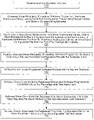
- FIG. 7 illustrates the process of configuring the reconfigurable test system 100 according to the preferred embodiment of the present invention.
- FIG. 8 presents a block diagram for a programmable trigger circuit 800 according to the one embodiment of the present invention.
- FIG. 1 Reconfigurable Test System
- FIG. 1 illustrates a reconfigurable test system 100 according to the preferred embodiment of the present invention.
- the reconfigurable test system and method of the present invention may be programmed to suit any desired test and/or measurement application.
- the reconfigurable test system 100 may be configured for controlling a thermal stress test for manufactured components.
- the reconfigurable test system may be coupled to thermal sensors and actuators in order to implement a thermal loading test procedure.
- the same reconfigurable test system 100 may be later reconfigured for performing vibration testing of some other manufactured device.
- the reconfigurable test system may be coupled to appropriate vibration generators and sensors in order to realize a vibration test procedure.
- the reconfigurable test system and method are used for telecommunication test applications, and this embodiment is discussed below.
- the present invention is not intended to be limited to telecommunication test applications, but can be used for any of various test and/or measurement applications as alluded to above.
- the following description describes the present invention in the specific domain of telecommunication testing.
- the reconfigurable test system 100 includes a host computer 110 coupled to a reconfigurable test instrument (RTI) 130 through an interconnecting bus 120 .
- RTI reconfigurable test instrument
- the term “RTI” or “instrument” is intended to include any of various types of devices such as a computer add-in card, an internal computer device, e.g., comprised on the computer motherboard, or an external device, among other configurations.
- the RTI 130 is configured for coupling to a unit under test (UUT) 150 through a communication medium 140 .
- unit under test 150 may comprise a plurality of separate entities being tested.
- the communication medium 140 may represent a plurality of distinct communication media.
- the RTI 130 preferably includes a reconfigurable hardware module, a reconfigurable front end, and optionally an embedded (i.e. local) processor with local memory as shown, e.g., in FIGS. 3A–3B .
- the RTI 130 may be programmed to suit any desired test application.
- the reconfigurable hardware module preferably includes one or more reconfigurable hardware devices such as Field Programmable Gate Arrays (FPGAs).
- FPGAs Field Programmable Gate Arrays
- the reconfigurable hardware module may be programmed to realize any desired hardware architecture.
- the reconfigurable front end may be programmed to interface with any desired types of signals using any desired line encoding scheme, voltage levels, etc. If an embedded processor is present on the RTI 130 , an additional measure of programmability is afforded by appropriate selection of the embedded instruction code to be executed by the embedded processor.
- the RTI may be programmed to operate with any desired type of UUT 150 , any desired communication medium 140 , any desired protocol(s) for signal exchange over the communication medium 140 , and any desired test procedure, etc.
- these reconfigurable technologies also allow the RTI 130 to be rapidly reprogrammed in response to changes in the UUT 150 , changes in the communication medium 140 , changes in the protocol(s) used for signal exchange over the communication medium, changes in the desired test procedure, etc.
- the host computer 110 is representative of any of a variety of computing devices such as personal computers, desktop computers, workstations, portable computers, laptop computers, etc.
- the RTI 130 is configured as an internal add-in board for insertion into a slot of the host computer 110 .
- the RTI 130 may reside external to host computer 110 , or may involve a combination of internal and external parts.
- the RTI 130 is situated at a location which is remote from host computer 110 .
- the RTI 130 may be located at a remote test site close to UUT 150 which may be hazardous or otherwise unsuitable for host computer 110 .
- the interconnecting bus 120 may be realized by any of various bus connectivity technologies such as, e.g., a Peripheral Component Interconnect (PCI) bus, a PXI bus, a Universal Serial Bus (USB), an IEEE 394 bus, etc., or any combination thereof.
- PCI Peripheral Component Interconnect
- PXI Peripheral Component Interconnect
- USB Universal Serial Bus
- IEEE 394 IEEE 394 bus
- the communication medium 140 is representative of any of a variety of physical media including, e.g., metallic wire/cable, optical fiber, the atmosphere, etc., or any combination thereof.
- the RTI 130 may include connectors such as screw terminals or spring loaded terminals for coupling to wires.
- the RTI 130 may include connectors for one or more types of conductive cable or optical fiber.
- the RTI 130 may include connectors for coupling to one or more external antennas for atmospheric transmission or reception of signals.
- Various embodiments of the RTI 130 are contemplated with varying numbers of connectors and varying combinations of connector types.
- the unit under test (UUT) 150 represents one or more devices, systems, components, or combination thereof which are to be tested. UUT 150 interacts with the RTI 130 through the communication medium 140 . UUT 150 may be a digital, analog, or a hybrid analog-digital device. In order to communicate with the RTI 130 , the UUT 150 may utilize any of a wide variety of communication protocols including proprietary internal protocols.
- the reconfigurable test system 100 of the present invention may be rapidly programmed, reprogrammed or reconfigured to operate with any desired protocol.
- the software configuration utility 500 preferably includes a graphical user interface which presents the user with a variety of choices such as, for example:
- a component selector 510 accesses one or more libraries 530 , 540 , 550 and/or 560 , and selects from the libraries a collection of files which match the user's selections.
- the component selector 510 selects a hardware architecture file from a hardware architecture library 550 , a front-end configuration file from a front-end configuration library 560 , a number of host driver modules from a host software library 530 , and optionally one or more embedded software programs from an embedded code library 540 .
- the libraries include files for any possible combination of user choices.
- the hardware architecture file is downloaded to the reconfigurable hardware module 325 ( FIGS. 3A–3B ) on the RTI 130 .
- the front end configuration file is downloaded to the reconfigurable front end 330 ( FIGS. 3A–3B ) on the RTI 130 .
- the host driver modules are registered with a host software driver 520 .
- the one or more embedded software programs are downloaded to embedded memory 310 ( FIGS. 3A–3B ) for execution by a local processor 305 ( FIGS. 3A–3B ) on the RTI 130 .
- the downloaded files and/or registered modules posits the reconfigurable test system 100 with the operational attributes selected by the user with the configuration utility 500 .
- a software test application executing on the host computer 110 controls and monitors the reconfigurable test system 100 by making calls to the software driver.
- the RTI 130 is capable of rapid reconfiguration of its operational/functional organization. Whenever the user desires to change some aspect of the reconfigurable test system 100 , he/she may invoke the software configuration utility and reprogram the reconfigurable test system 100 .
- FIG. 2 The Host Computer Architecture
- FIG. 2 provides one embodiment for the architecture of host computer 110 .
- the host computer 100 may have any of various system architectures as desired.
- Host computer 110 includes a host CPU 200 , system memory 210 , bus bridge 205 , expansion bus 120 , input devices such as mouse 215 and keyboard 220 , a non-volatile memory 225 , a display 235 and reconfigurable test instrument (RTI) 130 according to the present invention.
- Host computer 110 may also include one or more peripheral devices represented by peripheral device 230 .
- Bus bridge 205 is coupled to host CPU 200 , system memory 210 , and expansion bus 120 .
- Bus bridge 205 mediates the high speed transfer of digital data between any two of the host CPU 200 , system memory 210 and expansion bus 120 .
- the input devices, non-volatile memory 225 and peripheral device 230 are preferably coupled to the expansion bus 120 .
- Non-volatile memory 225 is representative of a variety of a variety of storage devices such as, e.g., disk drives, CD-ROM drives, zip drives, magnetic tape drives, optical storage, etc., or any combination thereof.
- the RTI 130 is configured for coupling to the expansion bus of host computer 110 .
- the RTI 130 executes a test procedure on UUT 150 .
- the RTI sends stimulus signals/patterns to the UUT 150 and receives response signals/patterns from the UUT 150 through the communication medium 140 .
- the host computer 110 or RTI 130 is able to either validate the UUT 110 or identify defects in the UUT 110 .
- the expansion bus 120 comprises a Peripheral Component Interconnect (PCI) bus or the PXI (PCI eXtensions for Instrumentation) bus.
- PCI Peripheral Component Interconnect
- PXI PCI eXtensions for Instrumentation
- the expansion bus 120 may be realized any of a variety of interconnecting buses or combination thereof.
- the expansion bus 120 comprises an Industry Standard Architecture (ISA) bus or Extended Industry Standard Architecture (EISA) bus.
- Non-volatile memory 225 stores one or more software programs according to the present invention which control the operation of host computer 110 . These software programs are loaded into system memory 210 prior to execution by host CPU 200 .
- the reconfigurable test instrument (RTI) 130 of the present invention may have any of a variety of architectures and forms of which several are illustrated in FIGS. 3A and 3B , and discussed below. While, the RTI 130 is discussed below in terms of telecommunications applications, it should be borne in mind that the RTI 130 may be used for any of various test applications.
- FIG. 3A The Reconfigurable test instrument (RTI) 130
- FIG. 3A is a block diagram of the reconfigurable test instrument (RTI) 130 according to the preferred embodiment of the present invention.
- the RTI 130 includes a reconfigurable hardware module (RHM) 325 , a reconfigurable front end (RFE) 330 and a local CPU or embedded processor 305 .
- RHM reconfigurable hardware module
- RFE reconfigurable front end
- a user/developer has the freedom to optimize the distribution of processing functions into the RHM 325 , RFE 330 , embedded program code for execution by local CPU 305 , and/or host program code for execution by host CPU 200 .
- Processing functions which require high-speed real-time processing are advantageously performed in reconfigurable hardware, i.e. in RHM 325 and/or RFE 330 .
- Real-time signal processing functions which are algorithmically complex may be performed in embedded software which is executed by the local CPU 305 .
- Non-real-time processing functions such as, e.g., the user interface, background data analysis and visualization may be performed in host software on the host CPU 200 .
- the RTI 130 includes local memory 310 , local (i.e. embedded) CPU 305 , bus interface 315 , bus connector 317 , internal bus 320 , reconfigurable hardware module 325 , reconfigurable front end (RFE) 330 , programmable clock generator 327 , and I/O connectors 335 .
- Local memory 310 , local CPU 305 , bus interface 315 , reconfigurable hardware module 325 , programmable clock generator 327 and reconfigurable front end 330 couple to internal bus 320 .
- Programmable clock generator (PCG) 327 couples to the reconfigurable hardware module 325 .
- Reconfigurable hardware module may have a dedicated coupling 326 to RFE 330 apart from internal bus 320 in order to facilitate higher speed data transfer.
- Bus interface 315 couples to bus connector 317 .
- Local CPU 305 may be directly coupled to local memory 310 through memory bus 306 .
- local CPU 305 may access local memory 310 even when internal bus 320 is busy with other transfer operations.
- RHM 325 may be coupled directly to local memory 310 .
- Bus connector 317 is configured for coupling to expansion bus 120 .
- I/O connectors 135 represent a collection of connectors for coupling to various kinds of communication media including, e.g., wires, cables, antennas, optical fibers, or any combination thereof.
- communication medium 140 represents a plurality of communication channels between the RTI 130 and UUT 150 .
- the user of reconfigurable test system 100 may configure the RTI 130 and a host software driver (i.e. software driver which is to run on host CPU 200 ) to operate with any combination of communication protocols for communicating with UUT 150 over the plurality of communication channels.
- Bus interface 315 is provided for mediating data transfer between the internal bus 320 and expansion bus 120 .
- Local CPU 305 executes instruction code stored in local memory 310 .
- Local memory 310 comprises Random Access Memory (RAM) and preferably also Read Only Memory (ROM), and stores program variables, data structures, buffers for use by local CPU 305 .
- RAM Random Access Memory
- ROM Read Only Memory
- Reconfigurable hardware module (RHM) 325 includes one or more programmable devices such as Field Programmable Gate Arrays (FPGAs). Thus, the RHM 325 includes one or more reconfigurable or programmable hardware elements whose interconnectivity and functionality may be programmed by downloading configuration information to the RHM 325 .
- the configuration information posits or configures the RHM 325 with a desired hardware architecture. For this reason, the configuration information downloaded to the RHM 325 is referred to herein as a hardware architecture file.
- the RHM 325 may be reprogrammed to achieve a new hardware architecture whenever desired.
- the host computer 110 maintains library 550 of hardware architecture files which represent a variety of different hardware architectures. Any of these hardware architecture files may be downloaded to the RHM 325 to achieve corresponding hardware architectures.
- the reconfigurable test system 100 includes a hardware design utility.
- the hardware design utility provides a graphical user design environment for developing a hardware architecture, and for compiling the hardware architecture into a hardware architecture file.
- the hardware design utility preferably includes a graphical programming interface in which a user may select and configure graphical icons which represent hardware elements, blocks, subsystems, etc. which are generally referred to as cells. The user graphically specifies the connections between hardware cells as for example by drawing a path between a terminal of one cell to a terminal of another cell using the mouse 215 .
- Examples of selectable hardware elements may include transistors, logic gates, flip-flops, etc, or function blocks such as add blocks, multiply blocks, etc.
- selectable hardware blocks may include registers, buffers, parallel-to-serial converters, serial-to-parallel converters, counters, clock frequency dividers, pattern detector circuits, edge detectors, multiplexers, demultiplexers, trigger circuits, shift registers, parity checkers, and arithmetic function circuits.
- selectable hardware subsystems may include input channels or output channels.
- the hardware design utility is LabVIEW graphical programming software available from National Instruments Corporation.
- the hardware design utility may use a hardware description language, such as VHDL.
- the resulting hardware diagram may be compiled to a hardware architecture file.
- the hardware architecture file may be downloaded to RHM 325 for immediate test system operation, or may be stored in the hardware architecture library 550 for later use.
- Programmable clock generator (PCG) 327 generates one or more clock signals which are supplied to RHM 325 .
- the frequencies of the one or more clock signals are programmable.
- Programming information may be supplied through internal bus 320 .
- PCG 327 may receive programming information from RHM 325 .
- the programmable clock generator 325 preferably includes a numerically controlled oscillator.
- Reconfigurable front end (RFE) 330 includes various reconfigurable digital and/or analog circuitry for reconfigurable interfacing of RHM 325 with the communication medium 140 .
- the front-end behavior of the RFE 330 is determined by configuration information supplied to the RFE 330 preferably through internal bus 320 . This configuration information is herein referred to as a front end configuration file.
- RFE 330 mediates the exchange of signals between RHM 325 and UUT 150 .
- RFE 330 receives one or more signals from the UUT 150 transmitted through the communication medium 140 over one or more communication channels.
- RFE 330 operates on, i.e. decodes, demodulates, conditions, and/or detects these signals in a manner determined by the front-end configuration file.
- the resultant digital signal(s) are provided to the RHM 325 preferably through dedicated coupling 326 .
- RFE 330 receives one or more digital signals supplied by the RHM 325 through the dedicated coupling 326 .
- the RFE 330 operates on, i.e. encodes, modulates, and/or conditions these digital signals in a manner determined by the front end configuration file.
- the RFE 330 then transmits the resultant signals to the UUT 150 through the communication medium 140 over one or more communication channels which are not necessarily the same as those mentioned above in the receive direction.
- Reconfigurable front end (RFE) 330 may be configured for receiving and transmitting any of various kinds of analog, digital, and/or multi-level signals through communication medium 140 , and for modulating and/or demodulating these signals according to their respective modalities.
- a multi-level signal refers to a signal that that may have multiple amplitude levels.
- a digital signal is a multi-level with two amplitude levels.
- RFE 300 preferably includes one or more programmable transceivers which allow operation with multilevel signals. The number of amplitude levels and the voltages of these amplitude levels are programmable preferably on a per channel basis.
- RFE 330 includes an array of programmable transceivers.
- Each programmable transceiver forms part of a serial channel as, e.g., serial channel 402 -K of FIG. 4B , and admits programming as either a receiver for an input channel or a transmitter for an output channel.
- the front end configuration file programs RFE 330 and determines such features of the programmable transceivers 410 such as (a) the directionality (input or output) of each programmable transceiver, (b) the line encoding scheme for each programmable transceiver, (c) the modulation or demodulation scheme to be used for each programmable transceiver, etc.
- the programmable transceivers 410 may be programmed to transmit or receive multi-level signals to/from the UUT 150 .
- programmable transceiver 410 -K (see FIG. 4B ) may be programmed as part of a serial output channel to drive conductor 425 -K with a multi-level signal. The number of levels and the voltages for each level of the multi-level signal are programmable.
- programmable transceiver 410 -K may be programmed as part of a serial input channel to receive from conductor 425 -K a multi-level signal. The number of levels to be expected and the nominal voltages for each level of the multilevel signal are programmable.
- RFE 330 may include programmable switching circuitry (not shown) for switching analog and/or digital signals between the conductors of I/O connectors 335 and the reconfigurable circuitry of the RFE 330 .
- RFE 330 may also include one or more A/D converters and D/A converters (not shown) for transmitting analog signals over one or more analog channels. Also RFE 330 may include modulation and demodulation circuitry for transmitting and receiving modulated signals. For example, RFE 330 may include FSK mod/demod circuitry for handling a number of FSK channels. The present invention contemplates the use of any of a variety of modulation schemes, and therefore RFE 330 may include any of a variety of mod/demod circuits.
- RFE 330 includes one or more Field Programmable Analog Arrays (FPAAs).
- FPAA is an integrated circuit which can be configured to implement various analog functions using a set of configurable analog blocks and a programmable interconnection network.
- the front end configuration file includes information for programming the FPAA(s).
- the hardware design utility described above may additionally provide a graphical FPAA design environment for designing an analog circuit diagram, and for compiling the analog circuit diagram into a FPAA definition file.
- the analog design environment allows the user to select and interconnect graphical icons using, e.g., the mouse 215 of host computer 110 .
- the interconnections may represent conductive paths.
- the graphical icons represent those analog elements, devices, blocks, or subsystems which are realizable in the FPAA(s).
- the resultant analog circuit diagram may be compiled into a FPAA definition file, and immediately downloaded to the FPAA(s), or stored in a library of such FPAA definition files for later use.
- the hardware design utility includes a graphical front end design environment which allows a user to configure the reconfigurable digital and/or analog hardware of the RFE 330 .
- the digital, analog and front-end design environments provided by the hardware design utility may be integrated into a single design environment.
- a user may be able to select both digital cells and analog cells, and interconnect these cells in one circuit diagram subject to any design constraints which may be imposed by the physical hardware, i.e. the RHM 325 and RFE 330 .
- the user may designate the target destination for each cell, block, or subsystem of the combined circuit diagram.
- the hardware design utility may be delegated the task of optimizing the distribution of cells, blocks, or subsystems between the various target destinations.
- Target destinations include the RHM 325 , the FFPA(s) in the RFE 330 , and the remaining hardware in the RFE 330 .
- Local CPU 305 executes a local control program which is stored in local memory 310 .
- Local CPU 305 may be variously referred to herein as the embedded CPU, the dedicated CPU, or the on-board CPU.
- the local control program may be variously referred to herein as the embedded software program or embedded instruction code.
- the local control program is downloaded to the local memory 310 by the software configuration utility 500 running on the host CPU 200 .
- local CPU 305 reads out-going data, i.e. data which is to be transmitted to UUT 150 , from system memory 210 and/or local memory 310 .
- Local CPU 305 supplies the out-going data to one or more output channels of the RHM 325 .
- the RHM 325 and RFE 330 then transmit the out-going data to UUT 150 .
- local CPU 305 reads in-coming data, i.e. data originating from the UUT 150 , from one or more input channels of the RHM 325 .
- the in-coming data is then transferred to system memory 210 and/or local memory 310 .
- the local CPU 305 may perform processing tasks on the in-coming data or out-going data as determined by the local control program.
- the reconfigurable test instrument (RTI) 130 allows a combination of software programmability by virtue of the local control program and hardware programmability by virtue of the configuration information downloaded to the RHM 325 and RFE 330 .
- the hardware architecture file downloaded to the RHM 325 determines the hardware personality of the RHM 325 .
- configuration information downloaded to the RFE 330 determines structure of the RFE 330 .
- reconfigurable test instrument 130 In the embodiment of reconfigurable test instrument 130 shown in FIG. 3A , the presence of a local CPU 305 implies that the reconfigurable test instrument 130 may operate with a measure of independence from host CPU 200 . In fact, the reconfigurable test instrument 130 may continue to perform its test control and monitoring functions if the host computer 110 is performing other functions or even if the host computer 110 crashes. Furthermore, reconfigurable test instrument 130 may be provided with its own power supply, and thus may continue to operate even when the host computer 110 loses power.
- FIG. 3B A Second Alternate Embodiment of RTI 130
- FIG. 3B presents a second alternate embodiment of the reconfigurable test instrument 130 .
- the reconfigurable hardware module (RHM) 325 couples to bus interface 315 , to reconfigurable front end (RFE) 330 , and to programmable clock generator (PCG) 327 .
- Bus interface 315 couples to bus connector 317 , while bus connector 317 is configured for coupling to expansion bus 120 .
- RFE 330 couples to I/O connectors 335 .
- I/O connectors 335 (or some subset of I/O connectors 335 ) couple to the unit under test (UUT) 150 through communication medium 140 .
- reconfigurable front end 330 may receive its programming information, i.e. the front-end configuration file, through RHM 325 .
- FIG. 4A The Programmable Hardware Module and Reconfigurable Front End
- FIG. 4A presents one embodiment of the RHM 325 and RFE 330 .
- RHM 325 and RFE 330 are organized to achieve a pair of serial communication channels 402 A and 402 B.
- the behavior of each serial channel is determined by the configuration information downloaded to RHM 325 and RFE 330 , i.e., the hardware architecture file and the front end configuration file respectively. While only two serial channels are depicted in FIG. 4A , RHM 325 and RFE 330 may be organized with an arbitrary number of serial channels by a natural extension of the principles herein described. It is noted that the serial channels 402 A and 402 B will be collectively referred to herein as the serial channels 402 .
- RHM 325 includes a pair of virtual channel slots, i.e., VCS 405 A and VCS 405 B.
- RFE 330 includes a corresponding pair of programmable transceivers, i.e., PT 410 A and PT 410 B. While only two virtual channel slots and two programmable transceivers are depicted in FIG. 4A , arbitrary numbers of virtual channel slots and programmable transceivers are contemplated.
- Each serial channel 402 includes a virtual channel slot 405 and a corresponding programmable transceiver 410 .
- serial channel 402 A includes virtual channel slot 405 A and programmable transceiver 410 A.
- the serial channels 402 A and 402 B couple to the UUT 150 through conductors 425 A and 425 B respectively. In the embodiment of FIG. 4A , conductors 425 A and 425 B form at least a portion of communication medium 140 .
- Each serial channel 402 may be independently programmed as either an input channel or output channel.
- the hardware architecture file downloaded to the RHM 325 determines the directionality (i.e. input or output) of each virtual channel slot.
- the front-end configuration file downloaded to the RFE 330 determines the directionality of each programmable transceiver in a manner which is consistent with the directionality of the corresponding virtual channel slot.
- each serial channel achieves a high-speed input or output channel for communication with the UUT 150 . High data transfer rates are attainable because the serial channels 402 are hardware programmed into the RHM 325 and 330 as opposed to being implement by a CPU in software.
- serial channel 402 A is an output channel and serial channel 402 B is an input channel.
- Out-going data i.e. data to be transmitted to the UUT 150 through conductor 425 A, is first transferred to the virtual channel slot 405 A over internal bus 320 .
- Virtual channel slot 405 A is preferably programmed to include an input buffer for temporarily storing the out-going data.
- Local CPU 305 or host CPU 200 may load the input buffer with out-going data.
- the virtual channel slot 405 A may then transfer the outgoing data to programmable transceiver 410 A over serial bus 408 A.
- Virtual channel slot 405 A is preferably programmed to include a parallel-to-serial converter for transforming the out-going data into a serial form.
- Programmable transceiver 410 A conditions, encodes, and/or modulates the out-going data in a manner determined by the front-end configuration file.
- the resultant signal is transmitted by programmable transceiver 410 A to UUT 150 over conductor 425 A.
- the out-going data may be encoded as a four-level signal, i.e., a signal with four discrete amplitude levels.
- the front-end configuration file may then specify the line encoding scheme to be four-level coding, and provide the four voltage levels for transmitting the signal data.
- An in-coming signal i.e., a signal transmitted from the UUT 150
- Programmable transceiver 410 B decodes, demodulates, and/or operates on the received signal in a manner determined by the front-end configuration file.
- the programmable transceiver 410 B may then supply a digital data stream to virtual channel slot 405 B over serial bus 408 B.
- Virtual channel slot 405 B is preferably programmed to include a serial-to-parallel converter for converting the data stream into parallel form.
- Virtual channel slot 405 B may store the received data in an output buffer.
- the output buffer may be configured as part of virtual channel slot 405 B or may reside external to the virtual channel slot 405 B.
- the output buffer may be read by local CPU 305 and/or host CPU 200 for further processing and/or storage of the received data.
- the received data may be transferred to system memory 210 , or local memory 310 .
- virtual channel slot 405 B may perform various operations on the received data as determined by the hardware architecture file.
- the virtual channel slot 405 B may be programmed to perform pattern detection, edge detection, parity checking, etc. on the received data stream.
- a pattern matching circuit encoded into the virtual channel slot 405 B may scan for the occurrence of a given pattern in the received data stream. Upon detection of the pattern, the pattern matching circuit asserts a pattern match signal.
- the pattern match signal may be used to trigger one or more other events.
- the pattern match circuit may be useful for detecting the start and/or end of a data frame.
- the search pattern may be programmed into a register or buffer of the pattern match circuit.
- programmable transceiver 410 B (and any of the programmable transceivers 410 ) may be programmed to decode the received signal as a multi-level signal.
- the front-end configuration file specifies the number of levels in the multi-level signal and the voltage value associated with each of the multiple levels.
- One or more of the virtual channel slots 405 may be programmed to include a triggering circuit to be described in detail somewhat later.
- the triggering circuit may receive various signals of interest to the user such as a pattern match signal, an edge detection signal, an external trigger, etc.
- the trigger circuit may generate a trigger signal as a function of the input signals.
- the trigger signal may be used to initiate or terminate the transmission and/or reception of channel data.
- the trigger signal may be supplied to virtual channel slot 405 A to initiate data transfer to the UUT 150 .
- the trigger signal may be supplied to virtual channel slot 405 B to initiate the buffering of received data.
- Virtual channel slot 405 A may be coupled to programmable transceiver 410 A by a control bus 407 A.
- the control bus 407 A allows the virtual channel slot 405 A to control various operations of the programmable transceiver 410 A.
- virtual channel slot 405 B may be coupled to programmable transceiver 410 B to control the operation of programmable transceiver 410 B.
- Programmable clock generator 327 is configured to generate a clock signal and supply the clock signal to the RHM 325 .
- the frequency or period of the clock signal is programmable.
- the local CPU 305 and/or the host CPU 200 may load the clock frequency or period information into a register of the PCG 327 .
- the PCG 327 generates a clock signal whose frequency is determined by the value stored in the register.
- One or more serial channels 402 may use the clock signal.
- the clock signal may be used to control synchronous reception or transmission of serial data.
- the PCG 327 may generate one or more clock signals each with a programmable clock rate.
- An external clock line 420 may be provided to the reconfigurable test instrument 130 .
- the external clock line 420 allows an external clock signal to be used in addition to or instead of the internal clock supplied by the PCG 327 .
- a first subset of the serial channels 402 may perform synchronous transfers based on the external clock, while a second subset of the serial channels 402 may perform synchronous transfers based on the internal clock.
- a third subset of serial channels may perform asynchronous transfers using digital phase locked loops to synchronize with an input serial stream.
- FIG. 4B An Arbitrary Number of Channels
- FIG. 4B presents one embodiment of reconfigurable hardware module (RHM) 325 and reconfigurable front end (RFE) 330 which together implement N serial channels.
- RHM 325 comprises N virtual channels slots 405 , i.e. virtual channel slots 405 - 1 through 405 -N.
- RFE 330 comprises N programmable transceivers 410 , i.e. programmable transceivers 410 - 1 through 410 -N.
- the generic serial channel i.e., serial channel 402 -K, includes a virtual channel slot 405 -K and a programmable transceiver 410 -K, and is coupled to a conductor 425 -K which forms a portion of communication medium 140 .
- Conductors 425 - 1 through 425 -N form communication medium 140 .
- FIG. 5 Host Software Architecture
- FIG. 5 illustrates the preferred embodiment of the host software architecture according to the present invention.
- the components of the host software architecture are preferably stored in non-volatile memory 225 which includes any of a variety of storage media such as a hard drive, a CD-ROM drive, a floppy drive, a zip drive, a tape drive, etc., or any combination thereof.
- the host software components are loaded from the non-volatile memory 225 into system memory 210 as they are needed.
- the software architecture comprises software configuration utility 500 , component selector 510 , software driver 520 , driver component library 530 , embedded software library 540 , hardware architecture library 550 , front end configuration library 560 , and software test application 565 .
- the software configuration utility 500 preferably comprises a graphical user interface (GUI) for configuring the reconfigurable test system 100 .
- GUI graphical user interface
- the software configuration utility 500 accepts user input 501 and sends graphical output 502 to the user through display 235 .
- the software configuration utility 500 sends commands to the component selector 510 in response to choices made by the user. In response to these commands, the component selector 510 selects files from the driver component library 530 , the embedded software library 540 , the hardware architecture library 550 , and the front-end configuration library, and registers these files with the software driver 520 .
- the software configuration utility 500 , the component selector 510 , and the software driver 520 programs execute on host CPU 200 .
- the software driver 520 comprises a collection of software routines which provide a software interface for interacting with peripheral devices including the reconfigurable test instrument 130 .
- Software programs including the software test application may call the driver routines in order to arrange data transfer to/from reconfigurable test instrument 130 and other peripheral devices as desired.
- the software driver 520 exchanges various control signals with the reconfigurable test instrument 130 .
- the exchange of control signals between software driver 520 and reconfigurable test instrument 130 is represented by control stream 570 .
- the control signals serve to direct the I/O activity of the reconfigurable test instrument 130 .
- software driver 520 exchanges data with the reconfigurable test instrument 130 .
- Data transfer activity between the software driver 520 and reconfigurable test instrument 130 is represented by data I/O stream 575 .
- software driver 520 downloads configuration information (to be described below) to the reconfigurable test instrument 130 . This download activity is represented by download stream 580 .
- the driver component library 530 comprises a collection of software modules which perform various functions which may be of interest to a user for building a test application. One or more of these software modules may be registered with the software driver 520 . After this registration, host programs including the software test application 565 may call the registered software modules.
- the driver component library 530 preferably includes software modules which perform functions such as protocol handling, fundamental test procedures, etc.
- Software test application 565 serves to control a test procedure in part by making calls to the software driver 520 , and especially to the driver software modules which have been registered in the software driver 520 in response to user configuration selections. For example, the software test application 565 may induce the transfer of data/control signals to/from UUT 150 through one or more serial channels by calling appropriate driver software modules of the software driver 520 .
- the driver component library 530 may include modules such as the following: module 531 for implementing the RS232 protocol; module 532 for implementing the HDLC protocol; module 533 for implementing the SLIP protocol; module 534 for implementing the ATM protocol; module 535 for implementing the X.25 protocol; module 536 for implementing a bit error rate test (BERT), and so on.
- the driver component library may include other modules for implementing other telecommunication protocols and other test procedures.
- new software modules may be added to the driver component library 530 .
- protocol handling may be implemented (a) by driver software modules as illustrated above, (b) by programming the RHM 325 with a hardware architecture file, (c) by programming the RFE 330 with a front-end configuration file, (d) by downloading embedded software programs for execution on local CPU 305 , or any combination thereof.
- the reconfigurable test system 100 allows a system user/developer to achieve an optimal distribution of protocol processing tasks to each of these reconfigurable targets.
- the configuration utility 500 preferably provides the user with a choice of one or more telecommunication protocols to be implemented by the reconfigurable test system 100 .
- the configuration utility also validates the compatibility of the one or more telecommunication protocols to guide the user in selection of appropriate combinations of protocols.
- the component selector 510 selects one or more user selected modules from the driver component library 530 and registers the selected modules with the software driver 520 .
- the software driver 520 has a flexible structure which allows software modules to be inserted to provide specific kinds of test functionality.
- the HDLC protocol is a superstructure imposed on top of RS232
- the SLIP protocol is a superstructure on top of HDLC.
- the software modules of the software component library reflect the compatibility structure of such hierarchical organizations.
- the RS232 module 531 , HDLC module 532 , and the SLIP module 533 may be simultaneously chosen by component selector 510 for incorporation into the software driver structure, and together they are capable of implementing the SLIP protocol.
- Block generation software can be used, such as LabVIEW or VHDL, to generate the above software modules or blocks.
- FIG. 6B Hardware Architecture Library
- FIG. 6B illustrates one embodiment of the hardware architecture library 550 which comprises a variety of hardware architecture files.
- Each hardware architecture file contains data which specifies a complete hardware architecture which can be downloaded to the reconfigurable hardware module (RHM) 325 subject to user selection.
- the reconfigurable hardware module 130 includes one or more programmable hardware elements such as Field Programmable Gate Arrays (FPGAs).
- the RHM 325 preferably includes sufficient gate capacity for programming at least two I/O channels.
- the reconfigurable hardware module 325 herein described may be naturally extended to any desired number of I/O channels.
- each hardware architecture file contains information for programming the virtual channel slots 405 of the RHM 325 with a particular I/O channel structure.
- the configuration utility 500 prompts the user to specify how the virtual channel slots 405 of the RHM 325 are to be configured. For example, in the case that RHM 325 includes two virtual slots 405 as shown in FIG. 4A , the configuration utility 500 allows the user to choose the directionality, i.e. input or output, for each of the virtual channel slots 405 A and 405 B. In addition, the configuration utility 500 allows the user to select between synchronous transfer or asynchronous transfer. A variety of other features may be provided for user selection.
- the hardware architecture library 550 contains hardware architecture files that span the set of possible combinations of user choices. For example, the hardware architecture file denoted Output/Input/Synch contains the configuration data to realize an output in virtual channel slot 405 A, an input in virtual channel slot 405 B, and synchronous transfer mode in both serial channels 402 .
- the embedded software library 540 preferably includes a rich variety of embedded software programs for performing processing and/or control tasks which may be of interest to the user. One or more of these embedded software programs may be downloaded to local memory 310 and executed by local CPU 305 .
- embedded software library 540 may include embedded software programs for handling any of a variety of protocols, for performing real-time signal processing tasks, etc.
- the software configuration utility 500 preferably allows the user to choose one or more of the embedded software programs for downloading to the reconfigurable test instrument 130 .
- the front end configuration library 560 preferably includes a collection of front end configuration files for achieving a rich variety of front end configurations.
- Each of these embedded software programs may be downloaded to the reconfigurable front end (RFE) 330 to realize a particular front-end operational structure.
- the front end configuration file preferably includes information for programming the FPAA(s).
- a front end configuration file includes information for programming the reconfigurable hardware of the RFE 330 .
- a front end configuration file preferably includes information for programming the directionality (i.e. input or output), line encoding scheme, etc. for each of the programmable transceivers 410 of the RFE 330 .
- FIG. 7 Configuration Flowchart
- FIG. 7 presents a flowchart for the configuration steps performed in the preferred embodiment of the present invention.
- the configuration utility 500 prompts the user for choices of system features such as, for example,
- the component selector 510 selects one or more driver modules from the driver component library 530 , one or more embedded software programs from the embedded software library 540 , a hardware architecture file from the hardware architecture library 550 , and a front end configuration file from the front end configuration library 560 as shown in step 720 .
- the user has the option of creating and/or modifying these components using any or all of the design utilities described above as indicated by step 715 .
- the components selected in step 720 may be those created and/or modified by the user in step 715 .
- the component selector 510 registers the selected one or more driver modules, one or more embedded software programs, hardware architecture file and front end configuration file with the software driver 520 as shown in step 730 .
- step 740 the software driver 520 loads the registered software modules into its internal structure.
- step 750 the software driver 520 downloads the registered embedded software program(s) to local memory 310 on the reconfigurable test instrument 130 .
- step 760 the software driver 520 downloads the registered hardware architecture file to the reconfigurable hardware module 325 in the reconfigurable test instrument 130 .
- step 770 the software driver downloads the registered front end configuration file to the reconfigurable front end 330 on the reconfigurable test instrument 130 . It is noted that steps 740 , 750 , 760 and 770 may be performed in any order.
- the entire process from user selection to system configuration is preferably performed in real-time and can be repeated whenever the user deems necessary. For example, if the user has finished testing a first device or first plurality of devices of a common type and desires to test a different type of device as the UUT 150 , the user reconfigures the reconfigurable test system 100 by entering new choices in the configuration utility 500 .
- the features of the configuration utilities are available programmatically, meaning that during a test operation the user could select new functionality using the GUI, or the program is created such that it automatically changes the configuration in response to some event.
- testing a new device will imply the use of a different telecommunication protocols and/or channel structure for signal exchange over communication medium 140 .
- the user may specify choices of one or more new telecommunication protocols, a new test scenario, and/or new hardware architecture using the configuration utility 500 .
- the user may create the program such that choices of one or more new telecommunication protocols, a new test scenario, and/or new hardware architecture are automatically selected and implemented by the program in response to one or more events that occur during program execution.
- driver modules are implemented in software using the driver modules and the embedded software modules.
- one or more driver modules from the driver component library 530 may be incorporated into the software driver 520 , and one or more embedded software modules may be downloaded to the local memory 310 for execution by the local CPU 305 .
- the input/output configuration of virtual channel slots 405 are determined by the hardware architecture file downloaded to the configuration information downloaded to the RHM 325 . For example, if the hardware architecture file denoted by Input/Output::Asynch in FIG. 6B is downloaded to the RHM 325 , virtual channel slot 405 A is thereby configured as an input channel, virtual channel slot 405 B is thereby configured as an output channel, and both channels are configured for asynchronous operation.
- Hardware architecture files which specify asynchronous operation may program a digital phase locked loop into one or more of the virtual channel slots 405 .
- digital phase locked loops may be included as part of the reconfigurable hardware of RFE 330 .
- the user creates a graphical program using a graphical programming environment, such as LabVIEW from National Instruments Corporation.
- the graphical programming environment preferably executes on the host CPU 200 .
- a portion of the graphical program is compiled into a hardware architecture file for downloading to the reconfigurable hardware module 325 which contains one or more FPGAs.
- a portion of the graphical program is compiled into a front end configuration file for downloading to the reconfigurable front end 330 .
- Another portion of the graphical program may be compiled into an embedded software program for downloading to local memory 305 and execution by local CPU 310 .
- Yet another portion of the graphical program may be compiled into software modules for registry/incorporation into the software driver 520 .
- portions of the graphical program may be compiled into instruction code for execution on host CPU 200 .
- the software test program described above may be generated from portions of the graphical program which are compiled into instruction code for the host CPU 200 .
- the local memory 310 preferably stores a kernel providing basic OS services, as well as a graphical programming system run-time engine for real-time execution of compiled graphical programs.
- the local memory 310 is also operable to receive and store a portion or all of a compiled graphical program for execution in the reconfigurable test instrument 130 .
- the embedded CPU 305 executes code and data from the embedded memory 310 to implement at least a portion of a virtual instrumentation or industrial automation function, such as a telecommunication test function.
- the user may specify which portions of the graphical program are to be targeted for the respective destinations: reconfigurable hardware module 325 , reconfigurable front end 330 , embedded software for execution by local CPU 200 , host driver modules for registry with the software driver 520 , or host program code.
- an optimization utility may be invoked to automatically optimize the distribution of portions of the graphical program to the various target destinations.
- the user may generate a desired configuration for the reconfigurable test system 100 .
- At least a portion of the one or more of the graphical programs are compiled for execution on the local CPU 305 and execute locally on the reconfigurable test instrument 130 via the local CPU 305 and local memory 310 , and at least a portion of the one or more graphical programs is translated or converted into a hardware executable format and downloaded to reconfigurable hardware module 325 which includes one or more FPGAs.
- FIG. 8 Programmable Triggering Circuitry
- FIG. 8 illustrates one embodiment of a programmable triggering circuit 800 according to the present invention.
- one or more of the hardware architecture files in the hardware architecture library may include programming information which defines programmable triggering circuit 800 .
- the user may be able to choose programmable triggering circuit 800 as one of the graphical icons for building a circuit diagram.
- such a hardware architecture file When downloaded to the RHM 325 , such a hardware architecture file posits the RHM 325 with the ability to various triggering functions.
- the trigger circuit 800 includes a first multiplexer M 1 and a second multiplexer M 2 .
- Each multiplexer is provided with a plurality of inputs denoted I 1 , I 2 , I 3 , and I 4 .
- the multiplexers M 1 and M 2 receive control or select inputs C 1 and C 2 respectively.
- the value asserted on control input C 1 determines which of inputs I 1 through I 4 is coupled to the output of multiplexer M 1 .
- control or select input C 2 determines which of the inputs I 5 through I 8 is coupled to the output of multiplexer M 2 .
- the outputs of the multiplexers M 1 and M 2 are supplied as inputs to combinational logic CL.
- Combinational Logic CL receives a control input C 3 which determines a combinational logic function which operates on the outputs of the multiplexers.
- the combinational logic CL is configured to perform an logical AND operation, or a logical OR operation depending on a value asserted on control input C 3 .
- the combinational logic CL is configured to perform additional logic functions which include any or all of the logical functions in two binary variables (A XOR B, A OR -B, . . . ).
- the output of combinational logic CL is supplied as an input to J/K flip-flop 810 .
- the output of J/K flip-flop 810 represents a dual-event triggering signal (i.e. a triggering signal which is sensitive to two input conditions) and comprises the output of the trigger circuit 800 .
- This output signal may be used to trigger the acquisition of data for an input channel and/or the transmission of data from a serial output channel.
- the signal at the output of the J/K flip-flop is referred to as the trigger signal.
- the trigger signal is coupled to a timer TMR.
- An output from the timer TMR is coupled to the reset input of the J/K flip-flop.
- the timer TMR is loaded with an initial count value through timer load line TL.
- the timer TMR In response to the rising edge of the trigger signal, the timer TMR starts to decrement its internal count value. When the count value reaches zero, the timer TMR asserts an output signal which resets the J/K flip-flop 810 . Thus, when the trigger signal is asserted, it remains in the asserted state for a period of time determined by the initial count value.
- the signals I 1 through I 4 and I 5 through I 8 are not necessarily distinct sets of signals.
- the signals I 1 through I 8 comprise various signals which may be of interest to a user in building a triggering signal.
- Signals I 1 through I 8 may represent signals such as a pattern match signal, an edge detection signal, an external trigger signal, etc.
- the signal I 1 may be a rising (or falling) edge detection signal provided by an edge detection circuit.
- the signal I 2 may be an external trigger signal (not shown in FIG. 7 ).
- the signal I 3 may be the output of a pattern detection circuit.
- the pattern detection circuit is configured to detect a serial data pattern occurring on a serial input channel (or output channel).
- the pattern detection circuit may be loaded with a search pattern which is to be compared with the input data stream from an input channel. When the given pattern is detected, the pattern detection circuit asserts a signal at its output which indicates the detected pattern.
- the trigger circuit 800 of the present invention enables the reconfigurable test instrument 130 to trigger on any desired combination of events represented by I 1 through I 8 .
- the control inputs C 1 , C 2 , and C 3 , and timer load line TL may be determined by control information asserted by the software driver 520 on normal control flow 570 and data I/O path 575 as well as by the hardware architecture file which is downloaded to the RHM 325 .
Abstract
Description
-
- (1) a desired number of serial channels to be programmed into the
RTI 130 for signal exchange with theUUT 150; - (2) a desired directionality (input/output) for each of the serial channels;
- (3) telecommunication protocols to be used for each of the serial channels;
- (3) a line encoding scheme to be used for driving each output channel, and voltage levels for driving multi-level output signals;
- (4) a line encoding scheme to be expected for receiving signals on each input channel, and voltage levels to be expected for receiving signals on each input channel;
- (5) an option for using synchronous data transfer versus asynchronous data transfer for each serial channel;
- (6) for each synchronous channel, a choice of whether an internally generated clock signal is to be used or an externally provided clock;
- (7) a choice of test scenario or test procedure which is to be applied to the
UUT 150.
- (1) a desired number of serial channels to be programmed into the
-
- (1) a desired number of
serial channels 402 to be programmed into theRTI 130 for signal exchange with theUUT 150; - (2) a desired directionality (input/output) for each of the
serial channels 402; - (3) telecommunication protocols to be used for each of the
serial channels 402; - (3) a line encoding scheme to be used for driving each output channel, and/or voltage levels for driving multi-level output signals;
- (4) a line encoding scheme to be expected for receiving signals on each input channel, and/or voltage levels to be expected for receiving signals on each input channel;
- (5) an option for using synchronous data transfer versus asynchronous data transfer for each serial channel;
- (6) for synchronous channel, whether an internally generated clock signal is to be used or an externally provided clock;
- (7) test type of test scenario or test procedure which is to be applied to the
UUT 150.
The configuration utility 500 preferably includes a graphical user interface to make the user interaction more natural and efficient. In one embodiment of the configuration utility 500, the configuration utility 500 provides indication of compatibility or incompatibility of the user's collection of choices. The user may thereby be able to make more informed choices of hardware and software configuration.
- (1) a desired number of
Claims (100)
Priority Applications (8)
| Application Number | Priority Date | Filing Date | Title |
|---|---|---|---|
| US10/034,565 US7152027B2 (en) | 1998-02-17 | 2001-10-19 | Reconfigurable test system |
| US10/055,241 US7290244B2 (en) | 1998-02-17 | 2001-10-29 | System and method for configuring a reconfigurable system |
| US10/058,150 US7085670B2 (en) | 1998-02-17 | 2001-10-29 | Reconfigurable measurement system utilizing a programmable hardware element and fixed hardware resources |
| US10/055,691 US7024660B2 (en) | 1998-02-17 | 2001-10-29 | Debugging a program intended to execute on a reconfigurable device using a test feed-through configuration |
| US10/839,862 US7743362B2 (en) | 1998-02-17 | 2004-05-06 | Automatic generation of application domain specific graphical programs |
| US11/037,652 US7627695B2 (en) | 1998-02-17 | 2005-01-18 | Network-based system for configuring a programmable hardware element in a system using hardware configuration programs generated based on a user specification |
| US11/230,787 US20060015862A1 (en) | 1998-02-17 | 2005-09-20 | Reconfigurable measurement system utilizing a programmable hardware element and fixed hardware resources |
| US12/551,641 US8069275B2 (en) | 1998-02-17 | 2009-09-01 | Network-based system for configuring a programmable hardware element in a measurement system using hardware configuration programs generated based on a user specification |
Applications Claiming Priority (3)
| Application Number | Priority Date | Filing Date | Title |
|---|---|---|---|
| US7480698P | 1998-02-17 | 1998-02-17 | |
| US09/229,695 US6311149B1 (en) | 1997-08-18 | 1999-01-13 | Reconfigurable test system |
| US10/034,565 US7152027B2 (en) | 1998-02-17 | 2001-10-19 | Reconfigurable test system |
Related Parent Applications (3)
| Application Number | Title | Priority Date | Filing Date |
|---|---|---|---|
| US09/229,695 Continuation US6311149B1 (en) | 1997-08-18 | 1999-01-13 | Reconfigurable test system |
| US09/229,695 Continuation-In-Part US6311149B1 (en) | 1997-08-18 | 1999-01-13 | Reconfigurable test system |
| US09/499,503 Continuation-In-Part US6608638B1 (en) | 1997-08-18 | 2000-02-07 | System and method for configuring a programmable hardware instrument to perform measurement functions utilizing estimation of the hardware implentation and management of hardware resources |
Related Child Applications (6)
| Application Number | Title | Priority Date | Filing Date |
|---|---|---|---|
| US10/055,691 Continuation US7024660B2 (en) | 1998-02-17 | 2001-10-29 | Debugging a program intended to execute on a reconfigurable device using a test feed-through configuration |
| US10/058,150 Continuation US7085670B2 (en) | 1998-02-17 | 2001-10-29 | Reconfigurable measurement system utilizing a programmable hardware element and fixed hardware resources |
| US10/058,150 Continuation-In-Part US7085670B2 (en) | 1998-02-17 | 2001-10-29 | Reconfigurable measurement system utilizing a programmable hardware element and fixed hardware resources |
| US10/055,241 Continuation US7290244B2 (en) | 1998-02-17 | 2001-10-29 | System and method for configuring a reconfigurable system |
| US10/101,507 Continuation US7016811B2 (en) | 1998-02-17 | 2002-03-19 | Network-based system for configuring a programmable hardware element in a measurement system using hardware configuration programs generated based on a user specification |
| US11/230,787 Continuation US20060015862A1 (en) | 1998-02-17 | 2005-09-20 | Reconfigurable measurement system utilizing a programmable hardware element and fixed hardware resources |
Publications (2)
| Publication Number | Publication Date |
|---|---|
| US20020055834A1 US20020055834A1 (en) | 2002-05-09 |
| US7152027B2 true US7152027B2 (en) | 2006-12-19 |
Family
ID=26756074
Family Applications (3)
| Application Number | Title | Priority Date | Filing Date |
|---|---|---|---|
| US10/034,565 Expired - Lifetime US7152027B2 (en) | 1998-02-17 | 2001-10-19 | Reconfigurable test system |
| US10/055,241 Expired - Lifetime US7290244B2 (en) | 1998-02-17 | 2001-10-29 | System and method for configuring a reconfigurable system |
| US10/055,691 Expired - Lifetime US7024660B2 (en) | 1998-02-17 | 2001-10-29 | Debugging a program intended to execute on a reconfigurable device using a test feed-through configuration |
Family Applications After (2)
| Application Number | Title | Priority Date | Filing Date |
|---|---|---|---|
| US10/055,241 Expired - Lifetime US7290244B2 (en) | 1998-02-17 | 2001-10-29 | System and method for configuring a reconfigurable system |
| US10/055,691 Expired - Lifetime US7024660B2 (en) | 1998-02-17 | 2001-10-29 | Debugging a program intended to execute on a reconfigurable device using a test feed-through configuration |
Country Status (1)
| Country | Link |
|---|---|
| US (3) | US7152027B2 (en) |
Cited By (66)
| Publication number | Priority date | Publication date | Assignee | Title |
|---|---|---|---|---|
| US20040006636A1 (en) * | 2002-04-19 | 2004-01-08 | Oesterreicher Richard T. | Optimized digital media delivery engine |
| US20070282767A1 (en) * | 2006-05-10 | 2007-12-06 | Fan-Tien Cheng | Method for Evaluating Reliance Level of a Virtual Metrology System |
| US20080109779A1 (en) * | 2006-10-18 | 2008-05-08 | Moriat Alain G | System Simulation and Graphical Data Flow Programming in a Common Environment |
| US20080147371A1 (en) * | 2006-12-13 | 2008-06-19 | Gupton Kyle P | User Defined Virtual Instruments in a Simulation Environment |
| US20090066427A1 (en) * | 2005-02-04 | 2009-03-12 | Aaron Brennan | Poly-phase frequency synthesis oscillator |
| US20090132857A1 (en) * | 2007-11-20 | 2009-05-21 | Hong Fu Jin Precision Industry (Shenzhen) Co., Ltd | System and method for testing an embedded system |
| US20090313187A1 (en) * | 2008-06-16 | 2009-12-17 | International Business Machines Corporation | Data pattern generation, modification and management utilizing a semantic network-based graphical interface |
| US20090309712A1 (en) * | 2008-06-16 | 2009-12-17 | International Business Machines Corporation | Pattern-driven communication architecture |
| US7681201B2 (en) | 2006-08-04 | 2010-03-16 | Lectronix | Method and system for integrating and controlling components and subsystems |
| US7737724B2 (en) | 2007-04-17 | 2010-06-15 | Cypress Semiconductor Corporation | Universal digital block interconnection and channel routing |
| US7761845B1 (en) | 2002-09-09 | 2010-07-20 | Cypress Semiconductor Corporation | Method for parameterizing a user module |
| US7770113B1 (en) | 2001-11-19 | 2010-08-03 | Cypress Semiconductor Corporation | System and method for dynamically generating a configuration datasheet |
| US7774190B1 (en) | 2001-11-19 | 2010-08-10 | Cypress Semiconductor Corporation | Sleep and stall in an in-circuit emulation system |
| US20100268493A1 (en) * | 2009-04-21 | 2010-10-21 | Yongjun Tae | Battery management system and driving method for the same |
| US7825688B1 (en) | 2000-10-26 | 2010-11-02 | Cypress Semiconductor Corporation | Programmable microcontroller architecture(mixed analog/digital) |
| US7844437B1 (en) | 2001-11-19 | 2010-11-30 | Cypress Semiconductor Corporation | System and method for performing next placements and pruning of disallowed placements for programming an integrated circuit |
| US7893724B2 (en) | 2004-03-25 | 2011-02-22 | Cypress Semiconductor Corporation | Method and circuit for rapid alignment of signals |
| US7899924B2 (en) | 2002-04-19 | 2011-03-01 | Oesterreicher Richard T | Flexible streaming hardware |
| US7937651B2 (en) | 2005-01-14 | 2011-05-03 | Microsoft Corporation | Structural editing operations for network forms |
| US7971139B2 (en) | 2003-08-06 | 2011-06-28 | Microsoft Corporation | Correlation, association, or correspondence of electronic forms |
| US7979856B2 (en) | 2000-06-21 | 2011-07-12 | Microsoft Corporation | Network-based software extensions |
| US8001459B2 (en) | 2005-12-05 | 2011-08-16 | Microsoft Corporation | Enabling electronic documents for limited-capability computing devices |
| US8010515B2 (en) | 2005-04-15 | 2011-08-30 | Microsoft Corporation | Query to an electronic form |
| US8026739B2 (en) | 2007-04-17 | 2011-09-27 | Cypress Semiconductor Corporation | System level interconnect with programmable switching |
| US8040266B2 (en) | 2007-04-17 | 2011-10-18 | Cypress Semiconductor Corporation | Programmable sigma-delta analog-to-digital converter |
| US8049569B1 (en) | 2007-09-05 | 2011-11-01 | Cypress Semiconductor Corporation | Circuit and method for improving the accuracy of a crystal-less oscillator having dual-frequency modes |
| US8069436B2 (en) | 2004-08-13 | 2011-11-29 | Cypress Semiconductor Corporation | Providing hardware independence to automate code generation of processing device firmware |
| US8067948B2 (en) | 2006-03-27 | 2011-11-29 | Cypress Semiconductor Corporation | Input/output multiplexer bus |
| US8069405B1 (en) | 2001-11-19 | 2011-11-29 | Cypress Semiconductor Corporation | User interface for efficiently browsing an electronic document using data-driven tabs |
| US8069428B1 (en) | 2001-10-24 | 2011-11-29 | Cypress Semiconductor Corporation | Techniques for generating microcontroller configuration information |
| US8074217B2 (en) | 2000-06-21 | 2011-12-06 | Microsoft Corporation | Methods and systems for delivering software |
| US8078894B1 (en) | 2007-04-25 | 2011-12-13 | Cypress Semiconductor Corporation | Power management architecture, method and configuration system |
| US8078970B1 (en) | 2001-11-09 | 2011-12-13 | Cypress Semiconductor Corporation | Graphical user interface with user-selectable list-box |
| US8085067B1 (en) | 2005-12-21 | 2011-12-27 | Cypress Semiconductor Corporation | Differential-to-single ended signal converter circuit and method |
| US8092083B2 (en) | 2007-04-17 | 2012-01-10 | Cypress Semiconductor Corporation | Temperature sensor with digital bandgap |
| US8103497B1 (en) | 2002-03-28 | 2012-01-24 | Cypress Semiconductor Corporation | External interface for event architecture |
| US8103496B1 (en) | 2000-10-26 | 2012-01-24 | Cypress Semicondutor Corporation | Breakpoint control in an in-circuit emulation system |
| US8117552B2 (en) * | 2003-03-24 | 2012-02-14 | Microsoft Corporation | Incrementally designing electronic forms and hierarchical schemas |
| US8120408B1 (en) | 2005-05-05 | 2012-02-21 | Cypress Semiconductor Corporation | Voltage controlled oscillator delay cell and method |
| US8130025B2 (en) | 2007-04-17 | 2012-03-06 | Cypress Semiconductor Corporation | Numerical band gap |
| US8149048B1 (en) | 2000-10-26 | 2012-04-03 | Cypress Semiconductor Corporation | Apparatus and method for programmable power management in a programmable analog circuit block |
| US8160864B1 (en) | 2000-10-26 | 2012-04-17 | Cypress Semiconductor Corporation | In-circuit emulator and pod synchronized boot |
| US20120110525A1 (en) * | 2010-11-02 | 2012-05-03 | Global Unichip Corporation | Hybrid electronic design system and reconfigurable connection matrix thereof |
| US8176296B2 (en) | 2000-10-26 | 2012-05-08 | Cypress Semiconductor Corporation | Programmable microcontroller architecture |
| US8200975B2 (en) | 2005-06-29 | 2012-06-12 | Microsoft Corporation | Digital signatures for network forms |
| US8402313B1 (en) | 2002-05-01 | 2013-03-19 | Cypress Semiconductor Corporation | Reconfigurable testing system and method |
| US8487879B2 (en) | 2004-10-29 | 2013-07-16 | Microsoft Corporation | Systems and methods for interacting with a computer through handwriting to a screen |
| US8499270B1 (en) | 2007-04-25 | 2013-07-30 | Cypress Semiconductor Corporation | Configuration of programmable IC design elements |
| US8516025B2 (en) | 2007-04-17 | 2013-08-20 | Cypress Semiconductor Corporation | Clock driven dynamic datapath chaining |
| US8527949B1 (en) | 2001-11-19 | 2013-09-03 | Cypress Semiconductor Corporation | Graphical user interface for dynamically reconfiguring a programmable device |
| US8605613B2 (en) | 2010-12-15 | 2013-12-10 | Apple Inc. | Mobile hardware and network environment simulation |
| US8756565B2 (en) | 2012-02-17 | 2014-06-17 | National Instruments Corporation | Modifying a target system configuration to utilize a different synchronization module for performing synchronization among multiple programmable hardware elements |
| US8776019B2 (en) | 2008-12-05 | 2014-07-08 | Invensys Systems, Inc. | Configurator with embedded firmware for offline instrument user settings implementation |
| US8788959B1 (en) | 2007-04-25 | 2014-07-22 | Cypress Semiconductor Corporation | System and method for monitoring a target device |
| US8892993B2 (en) | 2003-08-01 | 2014-11-18 | Microsoft Corporation | Translation file |
| US8918729B2 (en) | 2003-03-24 | 2014-12-23 | Microsoft Corporation | Designing electronic forms |
| US8996938B2 (en) | 1998-03-25 | 2015-03-31 | Intellectual Ventures I Llc | On-chip service processor |
| US9229917B2 (en) | 2003-03-28 | 2016-01-05 | Microsoft Technology Licensing, Llc | Electronic form user interfaces |
| US9448964B2 (en) | 2009-05-04 | 2016-09-20 | Cypress Semiconductor Corporation | Autonomous control in a programmable system |
| US9564902B2 (en) | 2007-04-17 | 2017-02-07 | Cypress Semiconductor Corporation | Dynamically configurable and re-configurable data path |
| US9720805B1 (en) * | 2007-04-25 | 2017-08-01 | Cypress Semiconductor Corporation | System and method for controlling a target device |
| US9910086B2 (en) | 2012-01-17 | 2018-03-06 | Allen Czamara | Test IP-based A.T.E. instrument architecture |
| US10698662B2 (en) | 2001-11-15 | 2020-06-30 | Cypress Semiconductor Corporation | System providing automatic source code generation for personalization and parameterization of user modules |
| US11200155B2 (en) * | 2020-04-09 | 2021-12-14 | The Toronto-Dominion Bank | System and method for automated application testing |
| US20220018896A1 (en) * | 2020-07-20 | 2022-01-20 | Tektronix, Inc. | Test and measurement instrument accessory with reconfigurable processing component |
| US11619920B2 (en) | 2019-04-03 | 2023-04-04 | Rohde & Schwarz Gmbh & Co. Kg | Method of customized setting as well as measurement system |
Families Citing this family (310)
| Publication number | Priority date | Publication date | Assignee | Title |
|---|---|---|---|---|
| US8352400B2 (en) | 1991-12-23 | 2013-01-08 | Hoffberg Steven M | Adaptive pattern recognition based controller apparatus and method and human-factored interface therefore |
| US7266725B2 (en) | 2001-09-03 | 2007-09-04 | Pact Xpp Technologies Ag | Method for debugging reconfigurable architectures |
| DE19651075A1 (en) | 1996-12-09 | 1998-06-10 | Pact Inf Tech Gmbh | Unit for processing numerical and logical operations, for use in processors (CPU's), multi-computer systems, data flow processors (DFP's), digital signal processors (DSP's) or the like |
| DE19654595A1 (en) | 1996-12-20 | 1998-07-02 | Pact Inf Tech Gmbh | I0 and memory bus system for DFPs as well as building blocks with two- or multi-dimensional programmable cell structures |
| ATE243390T1 (en) | 1996-12-27 | 2003-07-15 | Pact Inf Tech Gmbh | METHOD FOR INDEPENDENT DYNAMIC LOADING OF DATA FLOW PROCESSORS (DFPS) AND COMPONENTS WITH TWO- OR MULTI-DIMENSIONAL PROGRAMMABLE CELL STRUCTURES (FPGAS, DPGAS, O.L.) |
| US6542998B1 (en) | 1997-02-08 | 2003-04-01 | Pact Gmbh | Method of self-synchronization of configurable elements of a programmable module |
| US8686549B2 (en) | 2001-09-03 | 2014-04-01 | Martin Vorbach | Reconfigurable elements |
| DE19861088A1 (en) | 1997-12-22 | 2000-02-10 | Pact Inf Tech Gmbh | Repairing integrated circuits by replacing subassemblies with substitutes |
| US7743362B2 (en) * | 1998-02-17 | 2010-06-22 | National Instruments Corporation | Automatic generation of application domain specific graphical programs |
| US7966078B2 (en) * | 1999-02-01 | 2011-06-21 | Steven Hoffberg | Network media appliance system and method |
| US8230411B1 (en) | 1999-06-10 | 2012-07-24 | Martin Vorbach | Method for interleaving a program over a plurality of cells |
| US6560554B1 (en) * | 1999-10-11 | 2003-05-06 | Tektronix, Inc. | Automatic testing |
| EP2226732A3 (en) | 2000-06-13 | 2016-04-06 | PACT XPP Technologies AG | Cache hierarchy for a multicore processor |
| US7725860B1 (en) * | 2000-06-19 | 2010-05-25 | Herman Kwong | Contact mapping using channel routing |
| US8058899B2 (en) | 2000-10-06 | 2011-11-15 | Martin Vorbach | Logic cell array and bus system |
| US20020133842A1 (en) * | 2000-12-08 | 2002-09-19 | Leviten Michael W. | Transgenic mice containing deubiquitinated enzyme gene disruptions |
| JP4125475B2 (en) * | 2000-12-12 | 2008-07-30 | 株式会社東芝 | RTL generation system, RTL generation method, RTL generation program, and semiconductor device manufacturing method |
| US7197505B2 (en) * | 2000-12-22 | 2007-03-27 | Star Bridge Systems, Inc. | Multi-dimensional recursive wavefront behavioral synthesis |
| US9037807B2 (en) | 2001-03-05 | 2015-05-19 | Pact Xpp Technologies Ag | Processor arrangement on a chip including data processing, memory, and interface elements |
| US7444531B2 (en) | 2001-03-05 | 2008-10-28 | Pact Xpp Technologies Ag | Methods and devices for treating and processing data |
| US7844796B2 (en) | 2001-03-05 | 2010-11-30 | Martin Vorbach | Data processing device and method |
| US7134122B1 (en) * | 2001-05-31 | 2006-11-07 | Oracle International Corporation | One click deployment |
| EP1402382B1 (en) | 2001-06-20 | 2010-08-18 | Richter, Thomas | Data processing method |
| CA2704252C (en) | 2001-07-26 | 2011-09-27 | Irise | System and process for interacting with a user to define a behavior of a portion of an interactive presentation |
| DE10139610A1 (en) * | 2001-08-11 | 2003-03-06 | Daimler Chrysler Ag | Universal computer architecture |
| US7594220B2 (en) * | 2001-08-14 | 2009-09-22 | National Instruments Corporation | Configuration diagram with context sensitive connectivity |
| US6876368B2 (en) | 2001-08-14 | 2005-04-05 | National Instruments Corporation | System and method for deploying a graphical program to a PDA device |
| US7996827B2 (en) | 2001-08-16 | 2011-08-09 | Martin Vorbach | Method for the translation of programs for reconfigurable architectures |
| CA2458643A1 (en) * | 2001-08-17 | 2003-02-27 | Incyte Genomics, Inc. | Nucleic-acid associated proteins |
| US7434191B2 (en) | 2001-09-03 | 2008-10-07 | Pact Xpp Technologies Ag | Router |
| US8686475B2 (en) | 2001-09-19 | 2014-04-01 | Pact Xpp Technologies Ag | Reconfigurable elements |
| US8104017B2 (en) | 2001-10-25 | 2012-01-24 | The Mathworks, Inc. | Traceability in a modeling environment |
| US20030088858A1 (en) * | 2001-11-07 | 2003-05-08 | International Business Machines Corporation | Closed-loop design methodology for matching customer requirements to software design |
| US6966039B1 (en) * | 2001-11-19 | 2005-11-15 | Cypress Semiconductor Corp. | Method for facilitating microcontroller programming |
| US7337407B1 (en) | 2001-11-19 | 2008-02-26 | Cypress Semiconductor Corporation | Automatic application programming interface (API) generation for functional blocks |
| US7027070B2 (en) * | 2001-11-29 | 2006-04-11 | Agilent Technologies, Inc. | Systems and methods for manipulating a graphical display of a printed circuit board model for an automated x-ray inspection system |
| US20030110040A1 (en) * | 2001-12-07 | 2003-06-12 | Creative Logic Solutions Inc. | System and method for dynamically changing software programs by voice commands |
| US6671869B2 (en) * | 2001-12-12 | 2003-12-30 | Scott A. Davidson | Method and apparatus for graphically programming a programmable circuit |
| US7356773B1 (en) * | 2001-12-27 | 2008-04-08 | Expertune, Inc. | Wizard builder, for application software, building a setup wizard which sets up a defacto interface between the application program and monitoring or control equipment |
| US7139687B2 (en) * | 2001-12-31 | 2006-11-21 | The Mathworks, Inc. | Adaptive lookup table: a graphical simulation component for recursively updating numeric data stored in table form |
| AU2003208266A1 (en) | 2002-01-19 | 2003-07-30 | Pact Xpp Technologies Ag | Reconfigurable processor |
| US7290277B1 (en) * | 2002-01-24 | 2007-10-30 | Avago Technologies General Ip Pte Ltd | Control of authentication data residing in a network device |
| WO2003071432A2 (en) | 2002-02-18 | 2003-08-28 | Pact Xpp Technologies Ag | Bus systems and method for reconfiguration |
| US8914590B2 (en) | 2002-08-07 | 2014-12-16 | Pact Xpp Technologies Ag | Data processing method and device |
| US6934597B1 (en) * | 2002-03-26 | 2005-08-23 | Lsi Logic Corporation | Integrated circuit having integrated programmable gate array and method of operating the same |
| US7158924B2 (en) * | 2002-04-04 | 2007-01-02 | International Business Machines Corporation | Dynamic loading of C-API HDL model instrumentation |
| US7206732B2 (en) * | 2002-04-04 | 2007-04-17 | International Business Machines Corporation | C-API instrumentation for HDL models |
| US7203633B2 (en) | 2002-04-04 | 2007-04-10 | International Business Machines Corporation | Method and system for selectively storing and retrieving simulation data utilizing keywords |
| US20040006635A1 (en) * | 2002-04-19 | 2004-01-08 | Oesterreicher Richard T. | Hybrid streaming platform |
| US20030204711A1 (en) * | 2002-04-29 | 2003-10-30 | Guess Alan J. | Method and system for restoring custom user configuration settings across a host application download |
| US6661724B1 (en) | 2002-06-13 | 2003-12-09 | Cypress Semiconductor Corporation | Method and system for programming a memory device |
| US7594181B2 (en) * | 2002-06-27 | 2009-09-22 | Siebel Systems, Inc. | Prototyping graphical user interfaces |
| US7657861B2 (en) | 2002-08-07 | 2010-02-02 | Pact Xpp Technologies Ag | Method and device for processing data |
| AU2003286131A1 (en) | 2002-08-07 | 2004-03-19 | Pact Xpp Technologies Ag | Method and device for processing data |
| AU2003268373A1 (en) * | 2002-09-04 | 2004-03-29 | Mentor Graphics (Holdings) Ltd. | Polymorphic computational system and method |
| US7062744B2 (en) * | 2002-09-04 | 2006-06-13 | Osann Jr Robert | Emulation solution for programmable instruction DSP |
| US7394284B2 (en) | 2002-09-06 | 2008-07-01 | Pact Xpp Technologies Ag | Reconfigurable sequencer structure |
| US8020148B2 (en) * | 2002-09-23 | 2011-09-13 | Telefonaktiebolaget L M Ericsson (Publ) | Bi-directional probing and testing of software |
| US20040093198A1 (en) * | 2002-11-08 | 2004-05-13 | Carbon Design Systems | Hardware simulation with access restrictions |
| US20040093516A1 (en) * | 2002-11-12 | 2004-05-13 | Hornbeek Marc William Anthony | System for enabling secure remote switching, robotic operation and monitoring of multi-vendor equipment |
| DE10313389A1 (en) * | 2003-03-25 | 2004-10-07 | Endress + Hauser Process Solutions Ag | Method for transferring software code from a control unit to a field device in process automation technology |
| US7085706B1 (en) | 2003-01-14 | 2006-08-01 | Xilinx, Inc. | Systems and methods of utilizing virtual input and output modules in a programmable logic device |
| US7159204B2 (en) * | 2003-01-28 | 2007-01-02 | Altera Corporation | System and method for design entry and synthesis in programmable logic devices |
| JP3951925B2 (en) * | 2003-01-31 | 2007-08-01 | セイコーエプソン株式会社 | Hardware / software co-verification method |
| JP4403794B2 (en) * | 2003-02-28 | 2010-01-27 | 株式会社デンソー | Inspection method, inspection apparatus and inspection program for control program |
| US20040201506A1 (en) * | 2003-04-10 | 2004-10-14 | Tianmo Lei | The Set Side Box |
| US7984434B1 (en) * | 2003-05-21 | 2011-07-19 | Altera Corporation | Nondestructive patching mechanism |
| US20040268320A1 (en) * | 2003-06-13 | 2004-12-30 | Camille Huin | Graphical computer programming for a digital signal processor |
| US7277971B2 (en) * | 2003-06-26 | 2007-10-02 | The Boeing Company | Method and apparatus for communicating data over a bus according to redefinable configurations |
| US7822589B2 (en) * | 2003-07-15 | 2010-10-26 | Agere Systems Inc. | Method and apparatus for automatic generation of multiple integrated circuit simulation configuration |
| US7500228B2 (en) * | 2003-07-18 | 2009-03-03 | Agere Systems Inc. | System and method for automatically generating a hierarchical register consolidation structure |
| US7272549B2 (en) * | 2003-08-05 | 2007-09-18 | At & T Knowledge Ventures, L.P. | Restoring base configuration on software testing computer |
| US8397205B2 (en) * | 2003-08-07 | 2013-03-12 | National Instruments Corporation | Graphically representing timing in a graphical program |
| US7584082B2 (en) * | 2003-08-07 | 2009-09-01 | The Mathworks, Inc. | Synchronization and data review system |
| US7444595B2 (en) * | 2003-08-13 | 2008-10-28 | National Instruments Corporation | Graphical programming system and method for creating and managing a scene graph |
| EP1676208A2 (en) | 2003-08-28 | 2006-07-05 | PACT XPP Technologies AG | Data processing device and method |
| US7730415B2 (en) * | 2003-09-05 | 2010-06-01 | Fisher-Rosemount Systems, Inc. | State machine function block with a user modifiable state transition configuration database |
| US7324856B1 (en) * | 2003-09-25 | 2008-01-29 | Rockwell Automation Technologies, Inc. | Autogeneration of code via human-machine interfaces (HMI) and self-building HMI |
| US8645927B2 (en) * | 2003-11-24 | 2014-02-04 | The Boeing Company | Methods and apparatus for simulation speedup |
| US7236918B2 (en) * | 2003-12-31 | 2007-06-26 | International Business Machines Corporation | Method and system for selective compilation of instrumentation entities into a simulation model of a digital design |
| US7536288B2 (en) | 2003-12-31 | 2009-05-19 | International Business Machines Corporation | Method, system and program product supporting user tracing in a simulator |
| US8683426B2 (en) * | 2005-06-28 | 2014-03-25 | The Mathworks, Inc. | Systems and methods for modeling execution behavior |
| US8793602B2 (en) | 2004-01-15 | 2014-07-29 | The Mathworks, Inc. | System and method for scheduling the execution of model components using model events |
| US7761794B1 (en) * | 2004-01-22 | 2010-07-20 | Cisco Technology, Inc. | Integrated audit and configuration techniques |
| US7394410B1 (en) * | 2004-02-13 | 2008-07-01 | Samplify Systems, Inc. | Enhanced data converters using compression and decompression |
| KR100536293B1 (en) * | 2004-02-17 | 2005-12-12 | 박현주 | chip design verification apparatus and method |
| CN101976051A (en) * | 2004-02-25 | 2011-02-16 | Bep技术公司 | Method of programming processing system |
| US7770147B1 (en) * | 2004-03-08 | 2010-08-03 | Adaptec, Inc. | Automatic generators for verilog programming |
| DE102004027033B4 (en) * | 2004-03-15 | 2009-07-02 | Dspace Digital Signal Processing And Control Engineering Gmbh | Influence device for control devices and method for influencing a control device |
| US20050240831A1 (en) * | 2004-03-31 | 2005-10-27 | Balkman William D | Universal controller and graphical user interface |
| TW200535602A (en) * | 2004-04-16 | 2005-11-01 | Hon Hai Prec Ind Co Ltd | A system and method for testing motherboards automatically |
| US7836426B2 (en) * | 2004-05-06 | 2010-11-16 | National Instruments Corporation | Automatic generation of application domain specific graphical programs |
| US7603506B2 (en) * | 2004-06-18 | 2009-10-13 | Broadcom Corporation | Motherboard with video data processing card capability |
| US7860582B2 (en) * | 2004-06-23 | 2010-12-28 | National Instruments Corporation | Compact modular embedded device |
| US20050289523A1 (en) * | 2004-06-24 | 2005-12-29 | Broadcom Corporation | Method and apparatus for transforming code of a non-proprietary program language into proprietary program language |
| US7612779B2 (en) * | 2004-06-25 | 2009-11-03 | Broadcom Corporation | Video data processing circuits and systems comprising programmable blocks or components |
| US7802229B2 (en) * | 2004-07-16 | 2010-09-21 | National Instruments Corporation | Timed loop with sequence frames structure for a graphical program |
| US7761847B2 (en) * | 2004-07-16 | 2010-07-20 | National Instruments Corporation | Timed sequence for a graphical program |
| US20060035621A1 (en) * | 2004-07-21 | 2006-02-16 | Marius Ghercioiu | Measurement device with modular communication interface |
| US20060045461A1 (en) * | 2004-08-06 | 2006-03-02 | Microsoft Corporation | Methods and apparatus for project management |
| US7095280B2 (en) * | 2004-08-16 | 2006-08-22 | National Instruments Corporation | Programmable gain instrumentation amplifier having improved dielectric absorption compensation and common mode rejection ratio |
| US7594226B2 (en) | 2004-08-16 | 2009-09-22 | National Instruments Corporation | Implementation of packet-based communications in a reconfigurable hardware element |
| US7369078B2 (en) * | 2004-08-16 | 2008-05-06 | National Instruments Corporation | Flexible converter interface for use in analog-to-digital and digital-to-analog systems |
| US7183854B2 (en) * | 2004-08-17 | 2007-02-27 | National Instruments Corporation | Programmable gain instrumentation amplifier including a composite amplifier for level shifting and improved signal-to-noise ratio |
| US7721260B2 (en) * | 2004-09-08 | 2010-05-18 | Kozio, Inc. | Embedded Test I/O Engine |
| US7676649B2 (en) * | 2004-10-01 | 2010-03-09 | Lockheed Martin Corporation | Computing machine with redundancy and related systems and methods |
| EP1805935B1 (en) * | 2004-10-08 | 2011-03-09 | TELEFONAKTIEBOLAGET LM ERICSSON (publ) | Persistent confirmed configuration method |
| US7392169B2 (en) * | 2004-10-21 | 2008-06-24 | International Business Machines Corporation | Method, system and program product for defining and recording minimum and maximum event counts of a simulation utilizing a high level language |
| US20060089826A1 (en) * | 2004-10-21 | 2006-04-27 | International Business Machines Corporation | Method, system and program product for defining and recording minimum and maximum count events of a simulation |
| EP1655663A1 (en) * | 2004-11-05 | 2006-05-10 | Siemens Aktiengesellschaft | Dataflow modelling in engineering systems |
| US20100174521A1 (en) * | 2004-12-03 | 2010-07-08 | Nxp B.V. | Data processing with circuit modeling |
| US7454325B2 (en) | 2004-12-07 | 2008-11-18 | International Business Machines Corporation | Method, system and program product for defining and recording threshold-qualified count events of a simulation by testcases |
| US20060123342A1 (en) * | 2004-12-08 | 2006-06-08 | International Business Machines Corporation | System and method for creating generic, reusable, and dynamic application program configuration wizards |
| US7441158B1 (en) | 2005-01-10 | 2008-10-21 | L-3 Communications Integrated Systems, L.P. | Embedded hardware debugging tool and associated method |
| US7392489B1 (en) | 2005-01-20 | 2008-06-24 | Altera Corporation | Methods and apparatus for implementing application specific processors |
| US7613858B1 (en) * | 2005-01-24 | 2009-11-03 | Altera Corporation | Implementing signal processing cores as application specific processors |
| JP4497015B2 (en) * | 2005-04-01 | 2010-07-07 | トヨタ自動車株式会社 | Thermal energy recovery device |
| US7627784B1 (en) * | 2005-04-06 | 2009-12-01 | Altera Corporation | Modular processor debug core connection for programmable chip systems |
| US7509250B2 (en) * | 2005-04-20 | 2009-03-24 | Honeywell International Inc. | Hardware key control of debug interface |
| US7480126B2 (en) * | 2005-04-27 | 2009-01-20 | National Instruments Corporation | Protection and voltage monitoring circuit |
| US7739668B2 (en) * | 2005-05-16 | 2010-06-15 | Texas Instruments Incorporated | Method and system of profiling applications that use virtual memory |
| US20070028216A1 (en) | 2005-07-28 | 2007-02-01 | Boss Gregory J | Systems and methods for embedded application test suites |
| GB0516763D0 (en) * | 2005-08-16 | 2005-09-21 | Ibm | A method,system and computer program product for rendering a graphical user interface |
| FR2890463B1 (en) * | 2005-09-08 | 2008-03-14 | Hazemeyer Sa Sa | DEVICE FOR DIGITAL REGULATION OF AN ELECTRICAL SYSTEM AND ELECTRICAL SYSTEM COMPRISING SUCH A DEVICE. |
| WO2007028226A1 (en) * | 2005-09-09 | 2007-03-15 | Ibm Canada Limited - Ibm Canada Limitee | Method and system for state machine translation |
| US7552043B2 (en) * | 2005-09-15 | 2009-06-23 | International Business Machines Corporation | Method, system and program product for selectively removing instrumentation logic from a simulation model |
| US7606950B2 (en) * | 2005-10-17 | 2009-10-20 | National Instruments Corporation | Graphical programs with direct memory access FIFO for controller/FPGA communications |
| US7945895B2 (en) * | 2005-10-17 | 2011-05-17 | National Instruments Corporation | Graphical programs with FIFO structure for controller/FPGA communications |
| US9043016B2 (en) | 2005-10-21 | 2015-05-26 | Deere & Company | Versatile robotic control module |
| US7849449B2 (en) * | 2005-12-05 | 2010-12-07 | National Instruments Corporation | Implementing a design flow for a programmable hardware element that includes a processor |
| US20070143465A1 (en) * | 2005-12-06 | 2007-06-21 | Gonzalez Roberta L | Connection Tapping |
| US20070136467A1 (en) * | 2005-12-06 | 2007-06-14 | Masci Joseph M | Device Substitution |
| US10884712B1 (en) | 2005-12-30 | 2021-01-05 | The Mathworks, Inc. | Component-based framework for generating device driver model elements |
| US9329840B1 (en) | 2005-12-30 | 2016-05-03 | The Mathworks, Inc. | Graphical programming of custom device drivers |
| TW200727174A (en) * | 2006-01-03 | 2007-07-16 | Tatung Co Ltd | Method of testing a hardware circuit block written in a hardware description language |
| EP1974265A1 (en) | 2006-01-18 | 2008-10-01 | PACT XPP Technologies AG | Hardware definition method |
| US20070220451A1 (en) * | 2006-03-16 | 2007-09-20 | Arizona Public Service Company | Method for modeling and documenting a network |
| JP4457083B2 (en) * | 2006-03-28 | 2010-04-28 | 富士通株式会社 | Self-test apparatus and method for reconfigurable device board |
| US7840726B2 (en) * | 2006-04-12 | 2010-11-23 | Dell Products L.P. | System and method for identifying and transferring serial data to a programmable logic device |
| US7353474B1 (en) * | 2006-04-18 | 2008-04-01 | Xilinx, Inc. | System and method for accessing signals of a user design in a programmable logic device |
| US7711537B2 (en) * | 2006-05-03 | 2010-05-04 | International Business Machines Corporation | Signals for simulation result viewing |
| US7493248B2 (en) * | 2006-05-08 | 2009-02-17 | International Business Machines Corporation | Method, system and program product supporting phase events in a simulation model of a digital system |
| US20080288919A1 (en) * | 2007-05-14 | 2008-11-20 | Microsoft Corporation | Encoding of Symbol Table in an Executable |
| US7984432B2 (en) * | 2006-05-30 | 2011-07-19 | Infineon Technologies Ag | Method for patching a read-only memory and a data processing system comprising a means of patching the read-only memory based on patch contexts |
| US7966182B2 (en) * | 2006-06-20 | 2011-06-21 | Lunis Orcutt | Voiced programming system and method |
| US20070299847A1 (en) * | 2006-06-22 | 2007-12-27 | Sun Microsystems, Inc. | System and method for instrumentation using a native-asset-interface repository |
| US7676475B2 (en) * | 2006-06-22 | 2010-03-09 | Sun Microsystems, Inc. | System and method for efficient meta-data driven instrumentation |
| US7734640B2 (en) | 2006-06-22 | 2010-06-08 | Oracle America, Inc. | Resource discovery and enumeration in meta-data driven instrumentation |
| US7711625B2 (en) * | 2006-06-22 | 2010-05-04 | Oracle America, Inc. | Asynchronous events in meta-data driven instrumentation |
| US20070299846A1 (en) * | 2006-06-22 | 2007-12-27 | Sun Microsystems, Inc. | System and method for meta-data driven instrumentation |
| US20080040466A1 (en) * | 2006-06-22 | 2008-02-14 | Sun Microsystems, Inc. | System and method for object-oriented meta-data driven instrumentation |
| US7562084B2 (en) * | 2006-06-22 | 2009-07-14 | Sun Microsystems, Inc. | System and method for mapping between instrumentation and information model |
| US7805507B2 (en) * | 2006-06-22 | 2010-09-28 | Oracle America, Inc. | Use of URI-specifications in meta-data driven instrumentation |
| US8418128B2 (en) * | 2006-06-29 | 2013-04-09 | Honeywell International Inc. | Graphical language compiler system |
| US7693257B2 (en) * | 2006-06-29 | 2010-04-06 | Accuray Incorporated | Treatment delivery optimization |
| JP2009543175A (en) * | 2006-07-04 | 2009-12-03 | コーニンクレッカ フィリップス エレクトロニクス エヌ ヴィ | Executing computer instructions with reconfigurable hardware |
| US7954059B2 (en) * | 2006-07-24 | 2011-05-31 | National Instruments Corporation | Automatic conversion of text-based code having function overloading and dynamic types into a graphical program for compiled execution |
| US7975233B2 (en) * | 2006-07-24 | 2011-07-05 | National Instruments Corporation | Automatic conversion of a textual language into a graphical program representation |
| US8612870B2 (en) * | 2006-08-04 | 2013-12-17 | National Instruments Corporation | Graphically specifying and indicating targeted execution in a graphical program |
| US7844908B2 (en) * | 2006-08-04 | 2010-11-30 | National Instruments Corporation | Diagram that visually indicates targeted execution |
| US7840904B2 (en) * | 2006-08-04 | 2010-11-23 | National Instruments Corporation | Execution target structure node for a graphical program |
| KR101496185B1 (en) * | 2006-08-24 | 2015-03-26 | 지멘스 인더스트리 인코포레이티드 | Devices, systems, and methods for configuring a programmable logic controller |
| JP2008059066A (en) * | 2006-08-29 | 2008-03-13 | Matsushita Electric Ind Co Ltd | Compiler apparatus and semiconductor integrated circuit device |
| US20080115028A1 (en) * | 2006-10-23 | 2008-05-15 | Samsung Electronics Co., Ltd. | Method and system for test verification of integrated circuit designs |
| US8683444B1 (en) * | 2006-12-11 | 2014-03-25 | Synopsys, Inc. | System and method of debugging multi-threaded processes |
| US7912694B2 (en) * | 2007-01-30 | 2011-03-22 | International Business Machines Corporation | Print events in the simulation of a digital system |
| US7926036B2 (en) * | 2007-04-26 | 2011-04-12 | Microsoft Corporation | Technologies for code failure proneness estimation |
| US8175099B2 (en) * | 2007-05-14 | 2012-05-08 | Microsoft Corporation | Embedded system development platform |
| CA3029603C (en) * | 2007-08-10 | 2022-05-17 | Smiths Medical Asd, Inc. | System for controlling medical devices |
| US8484611B2 (en) * | 2007-10-15 | 2013-07-09 | International Business Machines Corporation | Method and system for simplified assembly of information processing applications |
| US9143561B2 (en) | 2007-11-09 | 2015-09-22 | Topia Technology, Inc. | Architecture for management of digital files across distributed network |
| US8312426B2 (en) * | 2008-01-07 | 2012-11-13 | International Business Machines Corporation | Method and system for simplified service composition in web environment |
| US8141047B2 (en) * | 2008-01-07 | 2012-03-20 | International Business Machines Corporation | Dependent object framework for junit testing and software application component |
| US8245122B2 (en) * | 2008-01-08 | 2012-08-14 | International Business Machines Corporation | Method and system for modeling user requests, applications and components used in dynamic application assembly |
| US8239828B2 (en) * | 2008-01-08 | 2012-08-07 | International Business Machines Corporation | Method of recovering from software failures using replanning |
| DE102008017289B4 (en) * | 2008-03-03 | 2021-10-14 | Rohde & Schwarz GmbH & Co. Kommanditgesellschaft | Customizable gauge and method of customization |
| US8640149B2 (en) * | 2008-03-26 | 2014-01-28 | International Business Machines Corporation | Method and apparatus for dynamic web service composition and invocation |
| US8561025B1 (en) * | 2008-03-31 | 2013-10-15 | Apigee Corporation | Flow and module level detecting and debugging with inclusion of generated log statements |
| US8305903B1 (en) * | 2008-03-31 | 2012-11-06 | C Speed, Llc | Data acquisition system for test and measurement signals |
| US8949140B2 (en) * | 2008-04-21 | 2015-02-03 | International Business Machines Corporation | Method and system for dynamic software reconfiguration triggered by component- or system- initiated events |
| GB2462997B (en) * | 2008-04-23 | 2010-09-08 | Wolfson Microelectronics Plc | Method and apparatus for configuring a device |
| US8898624B2 (en) * | 2008-05-05 | 2014-11-25 | International Business Machines Corporation | Method and apparatus for simplified assembly of parametric information processing applications |
| US8539443B2 (en) * | 2008-05-13 | 2013-09-17 | National Instruments Corporation | Edit time analyzer in a loosely typed textual language |
| US8117589B2 (en) * | 2008-06-26 | 2012-02-14 | Microsoft Corporation | Metadata driven API development |
| EP2317350A4 (en) * | 2008-07-24 | 2012-09-26 | Yupo Corp | Light reflector, and planar light source device and illuminating device using light reflector |
| US8291390B2 (en) * | 2008-07-30 | 2012-10-16 | National Instruments Corporation | Testing a graphical program intended for a programmable hardware element |
| US20100030874A1 (en) * | 2008-08-01 | 2010-02-04 | Louis Ormond | System and method for secure state notification for networked devices |
| US20100030598A1 (en) * | 2008-08-01 | 2010-02-04 | Electronic Data Systems Corporation | Platform provisioning system and method |
| US8266254B2 (en) * | 2008-08-19 | 2012-09-11 | International Business Machines Corporation | Allocating resources in a distributed computing environment |
| US8327117B2 (en) * | 2008-08-29 | 2012-12-04 | Rolls-Royce Corporation | Reconfigurable FADEC with flash based FPGA control channel and ASIC sensor signal processor for aircraft engine control |
| US9123093B1 (en) * | 2008-08-29 | 2015-09-01 | Cognex Corporation | Vision inspection programming method and apparatus |
| EP2350818A4 (en) * | 2008-11-03 | 2013-07-10 | Enginelab Inc | System and method of dynamically building a behavior model on a hardware system |
| US8160857B2 (en) | 2008-12-16 | 2012-04-17 | International Business Machines Corporation | Selective compilation of a simulation model in view of unavailable higher level signals |
| US8453080B2 (en) * | 2008-12-16 | 2013-05-28 | International Business Machines Corporation | Model build in the presence of a non-binding reference |
| US8201137B1 (en) * | 2009-03-06 | 2012-06-12 | Cadence Design Systems, Inc. | Method and apparatus for AMS simulation of integrated circuit design |
| US8479161B2 (en) * | 2009-03-18 | 2013-07-02 | Oracle International Corporation | System and method for performing software due diligence using a binary scan engine and parallel pattern matching |
| US20120005693A1 (en) * | 2010-01-08 | 2012-01-05 | Cypress Semiconductor Corporation | Development, Programming, and Debugging Environment |
| WO2010129909A1 (en) | 2009-05-07 | 2010-11-11 | Cypress Semiconductor Corporation | Development, programming, and debugging environment |
| US8271944B2 (en) * | 2009-05-18 | 2012-09-18 | National Instruments Corporation | Hosting a graphical program execution system on an embedded device |
| US8423981B2 (en) | 2009-06-18 | 2013-04-16 | National Instruments Corporation | Compiling a graphical program having a textual language program portion for a real time target |
| US8479156B2 (en) * | 2009-06-18 | 2013-07-02 | National Instruments Corporation | Providing target specific information for textual code at edit time |
| US20110004589A1 (en) * | 2009-07-06 | 2011-01-06 | Rockwell Automation Technologies, Inc. | Diagnostics in a distributed directory system |
| JP5407631B2 (en) * | 2009-07-21 | 2014-02-05 | 富士ゼロックス株式会社 | Circuit information generation device, function execution system, and program |
| US8151218B2 (en) * | 2009-07-29 | 2012-04-03 | National Instruments Corporation | Evaluation of graphical program nodes |
| US9836376B2 (en) * | 2009-09-24 | 2017-12-05 | Contec, Llc | Method and system for automated test of end-user devices |
| US20110078510A1 (en) * | 2009-09-30 | 2011-03-31 | Virtera | Computer Software and Hardware Evaluation System and Device |
| US8423314B2 (en) * | 2009-11-18 | 2013-04-16 | National Instruments Corporation | Deterministic reconfiguration of measurement modules using double buffered DMA |
| US7908348B2 (en) * | 2009-11-30 | 2011-03-15 | General Electric Company | Dynamic installation and uninstallation system of renewable energy farm hardware |
| FR2956525B1 (en) * | 2010-02-16 | 2016-01-08 | Airbus Operations Sas | CONNECTING SYSTEM AND SIMULATOR USING SUCH A CONNECTION SYSTEM |
| US20110209116A1 (en) * | 2010-02-19 | 2011-08-25 | Embedded Logix, Inc. | Programming Method and System For DAQ-Containing Device |
| US20110225524A1 (en) * | 2010-03-10 | 2011-09-15 | Cifra Christopher G | Multi-Touch Editing in a Graphical Programming Language |
| US20110258569A1 (en) * | 2010-04-20 | 2011-10-20 | Microsoft Corporation | Display of filtered data via frequency distribution |
| US8719797B2 (en) * | 2010-05-18 | 2014-05-06 | Blackberry Limited | System and method for debugging dynamically generated code of an application |
| US20110289469A1 (en) * | 2010-05-21 | 2011-11-24 | Huang Thomas B | Virtual interconnection method and apparatus |
| US8739150B2 (en) * | 2010-05-28 | 2014-05-27 | Smartshift Gmbh | Systems and methods for dynamically replacing code objects via conditional pattern templates |
| US8316342B1 (en) * | 2010-06-02 | 2012-11-20 | Cadence Design Systems, Inc. | Method and apparatus for concurrent design of modules across different design entry tools targeted to a single layout |
| US8521483B1 (en) | 2010-06-02 | 2013-08-27 | Cadence Design Systems, Inc. | Method and apparatus for concurrent design of modules across different design entry tools targeted to single simulation |
| WO2012048162A2 (en) * | 2010-10-08 | 2012-04-12 | Irise | System and method for extending a visualization platform |
| JP5626786B2 (en) * | 2010-11-09 | 2014-11-19 | インターナショナル・ビジネス・マシーンズ・コーポレーションInternational Business Machines Corporation | Software development support method, software development support device, and software development support program |
| US8826260B2 (en) * | 2011-01-11 | 2014-09-02 | Intuit Inc. | Customization of mobile-application delivery |
| US8874397B2 (en) * | 2011-01-14 | 2014-10-28 | National Instruments Corporation | User-invoked calibration of modular system using an embedded calibration signal generator |
| CN102685931A (en) * | 2011-03-17 | 2012-09-19 | 中兴通讯股份有限公司 | Wireless communication transmission system and wireless communication transmission method based on software radio |
| US9104443B2 (en) * | 2011-03-31 | 2015-08-11 | GM Global Technology Operations LLC | Control software with programmable arrays that are configurable for vehicles having different propulsion system configurations |
| JP5691752B2 (en) * | 2011-04-01 | 2015-04-01 | セイコーエプソン株式会社 | Data rewriting method, data rewriting device and rewriting program |
| US8954920B2 (en) * | 2011-04-21 | 2015-02-10 | Haik Biglari | Apparatus for developing embedded software and a process for making the same |
| US8762113B2 (en) * | 2011-06-03 | 2014-06-24 | Sony Computer Entertainment America Llc | Method and apparatus for load testing online server systems |
| US8713482B2 (en) | 2011-07-28 | 2014-04-29 | National Instruments Corporation | Gestures for presentation of different views of a system diagram |
| US9047007B2 (en) | 2011-07-28 | 2015-06-02 | National Instruments Corporation | Semantic zoom within a diagram of a system |
| US8782525B2 (en) | 2011-07-28 | 2014-07-15 | National Insturments Corporation | Displaying physical signal routing in a diagram of a system |
| US9063673B2 (en) * | 2011-08-30 | 2015-06-23 | Uniquesoft, Llc | System and method for implementing application code from application requirements |
| US8671389B1 (en) * | 2011-09-27 | 2014-03-11 | Google Inc. | Web application resource manager on the web and localizable components |
| US10613506B2 (en) | 2012-01-06 | 2020-04-07 | General Electric Company | Apparatus and method for creating and presenting control logic |
| US20130227367A1 (en) * | 2012-01-17 | 2013-08-29 | Allen J. Czamara | Test IP-Based A.T.E. Instrument Architecture |
| JP5833502B2 (en) * | 2012-06-04 | 2015-12-16 | 株式会社アドバンテスト | Test program |
| US8650525B2 (en) * | 2012-06-22 | 2014-02-11 | Altera Corporation | Integrated circuit compilation |
| US8806085B2 (en) | 2012-08-09 | 2014-08-12 | Ge Intelligent Platforms, Inc. | Application specific integrated circuit (ASIC) disposed in input/output module connectable to programmable logic controller (PLC) based systems having plurality of connection paths |
| US20140059518A1 (en) * | 2012-08-24 | 2014-02-27 | Velocio Networks, Inc. | Method for Object Oriented Programming of Programmable Logic Controllers in Graphical Programming Languages |
| JP6210187B2 (en) * | 2012-10-23 | 2017-10-11 | セイコーエプソン株式会社 | Integrated circuit device, physical quantity measuring device, electronic device, and moving object |
| US9611797B2 (en) * | 2012-10-30 | 2017-04-04 | National Instruments Corporation | Direct injection flexible multiplexing scheme |
| US20140157238A1 (en) * | 2012-11-30 | 2014-06-05 | Microsoft Corporation | Systems and methods of assessing software quality for hardware devices |
| US9176852B2 (en) * | 2012-12-10 | 2015-11-03 | International Business Machines Corporation | Role-oriented testbed environments for use in test automation |
| US10162007B2 (en) | 2013-02-21 | 2018-12-25 | Advantest Corporation | Test architecture having multiple FPGA based hardware accelerator blocks for testing multiple DUTs independently |
| US11009550B2 (en) | 2013-02-21 | 2021-05-18 | Advantest Corporation | Test architecture with an FPGA based test board to simulate a DUT or end-point |
| US10161993B2 (en) | 2013-02-21 | 2018-12-25 | Advantest Corporation | Tester with acceleration on memory and acceleration for automatic pattern generation within a FPGA block |
| US20140236527A1 (en) * | 2013-02-21 | 2014-08-21 | Advantest Corporation | Cloud based infrastructure for supporting protocol reconfigurations in protocol independent device testing systems |
| US9952276B2 (en) | 2013-02-21 | 2018-04-24 | Advantest Corporation | Tester with mixed protocol engine in a FPGA block |
| US9122622B1 (en) | 2013-02-26 | 2015-09-01 | Digital Dynamics, Inc. | Configurable input/output controller system |
| US20140278328A1 (en) * | 2013-03-15 | 2014-09-18 | Nvidia Corporation | System, method, and computer program product for constructing a data flow and identifying a construct |
| US9286032B2 (en) | 2013-03-15 | 2016-03-15 | International Business Machines Corporation | Automated software composition |
| US9323502B2 (en) | 2013-03-15 | 2016-04-26 | Nvidia Corporation | System, method, and computer program product for altering a line of code |
| US9015643B2 (en) | 2013-03-15 | 2015-04-21 | Nvidia Corporation | System, method, and computer program product for applying a callback function to data values |
| US9171115B2 (en) | 2013-04-10 | 2015-10-27 | Nvidia Corporation | System, method, and computer program product for translating a common hardware database into a logic code model |
| US9015646B2 (en) | 2013-04-10 | 2015-04-21 | Nvidia Corporation | System, method, and computer program product for translating a hardware language into a source database |
| US9021408B2 (en) | 2013-04-10 | 2015-04-28 | Nvidia Corporation | System, method, and computer program product for translating a source database into a common hardware database |
| DE102013104320A1 (en) * | 2013-04-29 | 2014-10-30 | Dspace Digital Signal Processing And Control Engineering Gmbh | Flexible distribution of the I / O channels of a hardware component |
| US9445522B2 (en) * | 2013-05-03 | 2016-09-13 | Taeho Um | Structurally-embedded construction, design, and maintenance record data management system and related method |
| US9086688B2 (en) | 2013-07-09 | 2015-07-21 | Fisher-Rosemount Systems, Inc. | State machine function block with user-definable actions on a transition between states |
| CN103441677B (en) * | 2013-08-21 | 2015-09-16 | 中国人民解放军海军工程大学 | Intermediate frequency three level full-bridge direct current converter is pressed in modularization megawatt |
| GB201316073D0 (en) * | 2013-09-10 | 2013-10-23 | Pace Plc | System and method for communication between a programmer interface and an electronic device |
| US9182951B1 (en) * | 2013-10-04 | 2015-11-10 | Progress Software Corporation | Multi-ecosystem application platform as a service (aPaaS) |
| US10884603B2 (en) * | 2014-03-03 | 2021-01-05 | Life Technologies Corporation | Graphical user interface system and method for transferring data acquisition and analysis settings |
| US9250893B2 (en) * | 2014-05-14 | 2016-02-02 | Western Digital Technologies, Inc. | Virtualized and automated software build system |
| US20150339127A1 (en) * | 2014-05-23 | 2015-11-26 | National Instruments Corporation | Configuration Change Tracking for Measurement Devices |
| US9483282B1 (en) * | 2014-05-30 | 2016-11-01 | Altera Corporation | Methods and systems for run-time hardware configuration change management |
| US9195457B1 (en) * | 2014-06-11 | 2015-11-24 | Amazon Technologies, Inc. | Interactive application programming interface documentation |
| US10540180B2 (en) * | 2014-12-07 | 2020-01-21 | Lenovo Enterprise Solutions (Singapore) Pte. Ltd. | Reconfigurable processors and methods for collecting computer program instruction execution statistics |
| JP6125119B2 (en) * | 2015-03-26 | 2017-05-10 | 三菱電機株式会社 | System design support apparatus, system design support method, and system design support program |
| US9547479B2 (en) * | 2015-03-30 | 2017-01-17 | Keysight Technologies, Inc. | Method for adapting GUI-based instrument components in a visual programming language |
| US9836300B2 (en) * | 2015-06-16 | 2017-12-05 | Lear Corporation | Method for updating vehicle ECUs using differential update packages |
| ES2562153B2 (en) | 2015-08-10 | 2016-10-07 | Keysight Technologies Singapore (Holdings) Pte. Ltd. | System and hardware configuration method of programmable control, test and measurement instruments |
| US10038464B2 (en) * | 2015-08-20 | 2018-07-31 | GM Global Technology Operations LLC | Configurable communications module |
| US11593342B2 (en) | 2016-02-01 | 2023-02-28 | Smartshift Technologies, Inc. | Systems and methods for database orientation transformation |
| US9940218B2 (en) * | 2016-02-15 | 2018-04-10 | International Business Machines Corporation | Debugging optimized code using fat binary |
| US10779056B2 (en) | 2016-04-14 | 2020-09-15 | Contec, Llc | Automated network-based test system for set top box devices |
| US10462456B2 (en) | 2016-04-14 | 2019-10-29 | Contec, Llc | Automated network-based test system for set top box devices |
| US10585655B2 (en) | 2016-05-25 | 2020-03-10 | Smartshift Technologies, Inc. | Systems and methods for automated retrofitting of customized code objects |
| US10216599B2 (en) * | 2016-05-26 | 2019-02-26 | International Business Machines Corporation | Comprehensive testing of computer hardware configurations |
| US10223235B2 (en) | 2016-05-26 | 2019-03-05 | International Business Machines Corporation | Comprehensive testing of computer hardware configurations |
| US10067183B2 (en) | 2016-06-21 | 2018-09-04 | International Business Machines Corporation | Portion isolation architecture for chip isolation test |
| US20180032468A1 (en) * | 2016-08-01 | 2018-02-01 | Honeywell International Inc. | Apparatus and method for identifying and managing input/output (i/o) channel spares for control and instrumentation systems in industrial plants |
| US10089103B2 (en) | 2016-08-03 | 2018-10-02 | Smartshift Technologies, Inc. | Systems and methods for transformation of reporting schema |
| US9977725B2 (en) * | 2016-08-26 | 2018-05-22 | Cisco Technology, Inc. | Automatic classification and parallel processing of untested code in a protected runtime environment |
| US10353807B2 (en) * | 2016-08-26 | 2019-07-16 | Accenture Global Solutions Limited | Application development management |
| JP6624008B2 (en) * | 2016-10-27 | 2019-12-25 | 横河電機株式会社 | Engineering tool cooperation device, engineering tool cooperation method, engineering tool cooperation program and recording medium |
| US10284456B2 (en) | 2016-11-10 | 2019-05-07 | Contec, Llc | Systems and methods for testing electronic devices using master-slave test architectures |
| US10635766B2 (en) | 2016-12-12 | 2020-04-28 | International Business Machines Corporation | Simulation employing level-dependent multitype events |
| US11227090B2 (en) * | 2017-02-15 | 2022-01-18 | Michael Alexander Green | System and method for achieving functional coverage closure for electronic system verification |
| US10699046B2 (en) * | 2017-02-15 | 2020-06-30 | Michael Alexander Green | System and method for achieving functional coverage closure for electronic system verification |
| US11193803B2 (en) | 2018-02-02 | 2021-12-07 | Analog Devices International Unlimited Company | Measurement system |
| US10698674B2 (en) | 2018-02-06 | 2020-06-30 | Smartshift Technologies, Inc. | Systems and methods for entry point-based code analysis and transformation |
| US10528343B2 (en) | 2018-02-06 | 2020-01-07 | Smartshift Technologies, Inc. | Systems and methods for code analysis heat map interfaces |
| US10740075B2 (en) | 2018-02-06 | 2020-08-11 | Smartshift Technologies, Inc. | Systems and methods for code clustering analysis and transformation |
| US10725746B2 (en) * | 2018-03-05 | 2020-07-28 | Stmicroelectronics, Inc. | Method and apparatus for quick prototyping of embedded peripherals |
| JP2020052812A (en) * | 2018-09-27 | 2020-04-02 | 横河電機株式会社 | Engineering system and engineering method |
| CN109491666B (en) * | 2018-11-15 | 2021-04-27 | 华至云链科技(苏州)有限公司 | Internet of things protocol self-programming method based on artificial intelligence |
| US10976361B2 (en) | 2018-12-20 | 2021-04-13 | Advantest Corporation | Automated test equipment (ATE) support framework for solid state device (SSD) odd sector sizes and protection modes |
| US11137910B2 (en) | 2019-03-04 | 2021-10-05 | Advantest Corporation | Fast address to sector number/offset translation to support odd sector size testing |
| US11237202B2 (en) | 2019-03-12 | 2022-02-01 | Advantest Corporation | Non-standard sector size system support for SSD testing |
| US10802807B1 (en) | 2019-05-23 | 2020-10-13 | Xilinx, Inc. | Control and reconfiguration of data flow graphs on heterogeneous computing platform |
| US11556353B2 (en) * | 2019-06-24 | 2023-01-17 | International Business Machines Corporation | Selective enhancement of interactive configuration interfaces |
| TWI709757B (en) * | 2019-07-24 | 2020-11-11 | 儀騰科技有限公司 | Fiber-optics communication component test device |
| US10884847B1 (en) | 2019-08-20 | 2021-01-05 | Advantest Corporation | Fast parallel CRC determination to support SSD testing |
| CN110602426B (en) * | 2019-09-30 | 2021-06-08 | 华南理工大学 | Video image edge extraction system |
| CN110750359B (en) * | 2019-10-17 | 2022-07-15 | 中科寒武纪科技股份有限公司 | Hardware resource configuration method and device, cloud side equipment and storage medium |
| US11448521B2 (en) * | 2019-11-29 | 2022-09-20 | Rohde & Schwarz Gmbh & Co. Kg | System and method for performing measurements in a modular application environment |
| CN112416760B (en) * | 2020-11-11 | 2023-05-23 | 北京京航计算通讯研究所 | Module packaging method and device for universal test platform TestBench |
| CN113031541A (en) * | 2021-02-03 | 2021-06-25 | 浙江富安莱科技有限公司 | Intelligent production program transmission system |
| US20230319150A1 (en) * | 2022-03-23 | 2023-10-05 | Ciena Corporation | Method and apparatus to self-document configuration in distributed microservice architectures |
| CN114706376B (en) * | 2022-06-06 | 2022-08-26 | 南京宏泰半导体科技有限公司 | Hardware control device and method based on software decoupling |
| US11811681B1 (en) | 2022-07-12 | 2023-11-07 | T-Mobile Usa, Inc. | Generating and deploying software architectures using telecommunication resources |
Citations (30)
| Publication number | Priority date | Publication date | Assignee | Title |
|---|---|---|---|---|
| US4849880A (en) | 1985-11-18 | 1989-07-18 | John Fluke Mfg. Co., Inc. | Virtual machine programming system |
| US4901221A (en) | 1986-04-14 | 1990-02-13 | National Instruments, Inc. | Graphical system for modelling a process and associated method |
| US5005119A (en) * | 1987-03-02 | 1991-04-02 | General Electric Company | User interactive control of computer programs and corresponding versions of input/output data flow |
| US5109504A (en) | 1989-12-29 | 1992-04-28 | Texas Instruments Incorporated | Graphics program adaptor |
| US5164911A (en) * | 1989-12-15 | 1992-11-17 | Hewlett-Packard Company | Schematic capture method having different model couplers for model types for changing the definition of the schematic based upon model type selection |
| US5197016A (en) * | 1988-01-13 | 1993-03-23 | International Chip Corporation | Integrated silicon-software compiler |
| US5309556A (en) | 1986-03-07 | 1994-05-03 | Hewlett-Packard Company | Method for using interactive computer graphics to control electronic instruments |
| WO1994010627A1 (en) | 1992-11-05 | 1994-05-11 | Giga Operations Corporation | System for compiling algorithmic language source code into hardware |
| WO1994015311A1 (en) | 1992-12-28 | 1994-07-07 | Xilinx, Inc. | Method for entering state flow diagrams using schematic editor programs |
| US5437464A (en) | 1991-08-30 | 1995-08-01 | Kabushiki Kaisha Sega Enterprises | Data reading and image processing system for CD-ROM |
| US5497498A (en) | 1992-11-05 | 1996-03-05 | Giga Operations Corporation | Video processing module using a second programmable logic device which reconfigures a first programmable logic device for data transformation |
| WO1996014618A1 (en) | 1994-11-04 | 1996-05-17 | Medialink Technologies Corporation | A method and apparatus for controlling non-computer system devices by manipulating a graphical representation |
| US5541849A (en) | 1990-04-06 | 1996-07-30 | Lsi Logic Corporation | Method and system for creating and validating low level description of electronic design from higher level, behavior-oriented description, including estimation and comparison of timing parameters |
| US5555201A (en) | 1990-04-06 | 1996-09-10 | Lsi Logic Corporation | Method and system for creating and validating low level description of electronic design from higher level, behavior-oriented description, including interactive system for hierarchical display of control and dataflow information |
| US5566295A (en) | 1994-01-25 | 1996-10-15 | Apple Computer, Inc. | Extensible simulation system and graphical programming method |
| US5583749A (en) | 1994-11-30 | 1996-12-10 | Altera Corporation | Baseboard and daughtercard apparatus for reconfigurable computing systems |
| US5603043A (en) | 1992-11-05 | 1997-02-11 | Giga Operations Corporation | System for compiling algorithmic language source code for implementation in programmable hardware |
| US5630164A (en) * | 1992-02-27 | 1997-05-13 | Associative Measurements Pty. Ltd. | Scientific instrument emulator having a computer and an analog signal interface for real-time signal processing |
| US5638299A (en) | 1995-06-22 | 1997-06-10 | Miller; Keith | Light weight, self-contained programmable data-acquisition system |
| US5652875A (en) | 1993-09-27 | 1997-07-29 | Giga Operations Corporation | Implementation of a selected instruction set CPU in programmable hardware |
| US5684980A (en) | 1992-07-29 | 1997-11-04 | Virtual Computer Corporation | FPGA virtual computer for executing a sequence of program instructions by successively reconfiguring a group of FPGA in response to those instructions |
| US5732277A (en) | 1986-10-24 | 1998-03-24 | National Instruments Corporation | Graphical system for modelling a process and associated method |
| US5737235A (en) | 1995-05-02 | 1998-04-07 | Xilinx Inc | FPGA with parallel and serial user interfaces |
| US5784275A (en) | 1996-09-23 | 1998-07-21 | National Instruments Corporation | System and method for performing interface independent virtual instrumentation functions in a graphical data flow program |
| US5847955A (en) | 1994-05-04 | 1998-12-08 | National Instruments Corporation | System and method for controlling an instrumentation system |
| US6064409A (en) | 1993-09-22 | 2000-05-16 | National Instruments Corporation | System and method for providing audio probe and debugging features in a graphical data flow program |
| US6226776B1 (en) | 1997-09-16 | 2001-05-01 | Synetry Corporation | System for converting hardware designs in high-level programming language to hardware implementations |
| US6230307B1 (en) | 1998-01-26 | 2001-05-08 | Xilinx, Inc. | System and method for programming the hardware of field programmable gate arrays (FPGAs) and related reconfiguration resources as if they were software by creating hardware objects |
| US6311149B1 (en) * | 1997-08-18 | 2001-10-30 | National Instruments Corporation | Reconfigurable test system |
| US6564368B1 (en) * | 1998-10-01 | 2003-05-13 | Call Center Technology, Inc. | System and method for visual application development without programming |
Family Cites Families (14)
| Publication number | Priority date | Publication date | Assignee | Title |
|---|---|---|---|---|
| DE59107764D1 (en) | 1991-02-22 | 1996-06-05 | Siemens Ag | Programmable logic controller |
| ATE229671T1 (en) | 1991-02-28 | 2002-12-15 | Ass Measurement Pty Ltd | SCIENTIFIC EMULATOR DEVICE |
| JP2815281B2 (en) * | 1993-04-19 | 1998-10-27 | 株式会社ピーエフユー | Digital circuit design support system and method |
| US6023565A (en) * | 1996-03-29 | 2000-02-08 | Xilinx, Inc. | Method for configuring circuits over a data communications link |
| US6112020A (en) * | 1996-10-31 | 2000-08-29 | Altera Corporation | Apparatus and method for generating configuration and test files for programmable logic devices |
| US6009256A (en) | 1997-05-02 | 1999-12-28 | Axis Systems, Inc. | Simulation/emulation system and method |
| US6219628B1 (en) | 1997-08-18 | 2001-04-17 | National Instruments Corporation | System and method for configuring an instrument to perform measurement functions utilizing conversion of graphical programs into hardware implementations |
| US6247147B1 (en) * | 1997-10-27 | 2001-06-12 | Altera Corporation | Enhanced embedded logic analyzer |
| US6052524A (en) * | 1998-05-14 | 2000-04-18 | Software Development Systems, Inc. | System and method for simulation of integrated hardware and software components |
| US6282627B1 (en) * | 1998-06-29 | 2001-08-28 | Chameleon Systems, Inc. | Integrated processor and programmable data path chip for reconfigurable computing |
| US6539438B1 (en) * | 1999-01-15 | 2003-03-25 | Quickflex Inc. | Reconfigurable computing system and method and apparatus employing same |
| JP2001060210A (en) * | 1999-08-20 | 2001-03-06 | Nec Corp | Lsi verification method and device and recording medium |
| US6571373B1 (en) * | 2000-01-31 | 2003-05-27 | International Business Machines Corporation | Simulator-independent system-on-chip verification methodology |
| US6802026B1 (en) * | 2001-05-15 | 2004-10-05 | Xilinx, Inc. | Parameterizable and reconfigurable debugger core generators |
-
2001
- 2001-10-19 US US10/034,565 patent/US7152027B2/en not_active Expired - Lifetime
- 2001-10-29 US US10/055,241 patent/US7290244B2/en not_active Expired - Lifetime
- 2001-10-29 US US10/055,691 patent/US7024660B2/en not_active Expired - Lifetime
Patent Citations (31)
| Publication number | Priority date | Publication date | Assignee | Title |
|---|---|---|---|---|
| US4849880A (en) | 1985-11-18 | 1989-07-18 | John Fluke Mfg. Co., Inc. | Virtual machine programming system |
| US5309556A (en) | 1986-03-07 | 1994-05-03 | Hewlett-Packard Company | Method for using interactive computer graphics to control electronic instruments |
| US4901221A (en) | 1986-04-14 | 1990-02-13 | National Instruments, Inc. | Graphical system for modelling a process and associated method |
| US5732277A (en) | 1986-10-24 | 1998-03-24 | National Instruments Corporation | Graphical system for modelling a process and associated method |
| US5005119A (en) * | 1987-03-02 | 1991-04-02 | General Electric Company | User interactive control of computer programs and corresponding versions of input/output data flow |
| US5197016A (en) * | 1988-01-13 | 1993-03-23 | International Chip Corporation | Integrated silicon-software compiler |
| US5164911A (en) * | 1989-12-15 | 1992-11-17 | Hewlett-Packard Company | Schematic capture method having different model couplers for model types for changing the definition of the schematic based upon model type selection |
| US5109504A (en) | 1989-12-29 | 1992-04-28 | Texas Instruments Incorporated | Graphics program adaptor |
| US5541849A (en) | 1990-04-06 | 1996-07-30 | Lsi Logic Corporation | Method and system for creating and validating low level description of electronic design from higher level, behavior-oriented description, including estimation and comparison of timing parameters |
| US5555201A (en) | 1990-04-06 | 1996-09-10 | Lsi Logic Corporation | Method and system for creating and validating low level description of electronic design from higher level, behavior-oriented description, including interactive system for hierarchical display of control and dataflow information |
| US5437464A (en) | 1991-08-30 | 1995-08-01 | Kabushiki Kaisha Sega Enterprises | Data reading and image processing system for CD-ROM |
| US5630164A (en) * | 1992-02-27 | 1997-05-13 | Associative Measurements Pty. Ltd. | Scientific instrument emulator having a computer and an analog signal interface for real-time signal processing |
| US5684980A (en) | 1992-07-29 | 1997-11-04 | Virtual Computer Corporation | FPGA virtual computer for executing a sequence of program instructions by successively reconfiguring a group of FPGA in response to those instructions |
| US5603043A (en) | 1992-11-05 | 1997-02-11 | Giga Operations Corporation | System for compiling algorithmic language source code for implementation in programmable hardware |
| WO1994010627A1 (en) | 1992-11-05 | 1994-05-11 | Giga Operations Corporation | System for compiling algorithmic language source code into hardware |
| US5535342A (en) | 1992-11-05 | 1996-07-09 | Giga Operations Corporation | Pld connector for module having configuration of either first PLD or second PLD and reconfigurable bus for communication of two different bus protocols |
| US5497498A (en) | 1992-11-05 | 1996-03-05 | Giga Operations Corporation | Video processing module using a second programmable logic device which reconfigures a first programmable logic device for data transformation |
| WO1994015311A1 (en) | 1992-12-28 | 1994-07-07 | Xilinx, Inc. | Method for entering state flow diagrams using schematic editor programs |
| US6064409A (en) | 1993-09-22 | 2000-05-16 | National Instruments Corporation | System and method for providing audio probe and debugging features in a graphical data flow program |
| US5652875A (en) | 1993-09-27 | 1997-07-29 | Giga Operations Corporation | Implementation of a selected instruction set CPU in programmable hardware |
| US5566295A (en) | 1994-01-25 | 1996-10-15 | Apple Computer, Inc. | Extensible simulation system and graphical programming method |
| US5847955A (en) | 1994-05-04 | 1998-12-08 | National Instruments Corporation | System and method for controlling an instrumentation system |
| WO1996014618A1 (en) | 1994-11-04 | 1996-05-17 | Medialink Technologies Corporation | A method and apparatus for controlling non-computer system devices by manipulating a graphical representation |
| US5583749A (en) | 1994-11-30 | 1996-12-10 | Altera Corporation | Baseboard and daughtercard apparatus for reconfigurable computing systems |
| US5737235A (en) | 1995-05-02 | 1998-04-07 | Xilinx Inc | FPGA with parallel and serial user interfaces |
| US5638299A (en) | 1995-06-22 | 1997-06-10 | Miller; Keith | Light weight, self-contained programmable data-acquisition system |
| US5784275A (en) | 1996-09-23 | 1998-07-21 | National Instruments Corporation | System and method for performing interface independent virtual instrumentation functions in a graphical data flow program |
| US6311149B1 (en) * | 1997-08-18 | 2001-10-30 | National Instruments Corporation | Reconfigurable test system |
| US6226776B1 (en) | 1997-09-16 | 2001-05-01 | Synetry Corporation | System for converting hardware designs in high-level programming language to hardware implementations |
| US6230307B1 (en) | 1998-01-26 | 2001-05-08 | Xilinx, Inc. | System and method for programming the hardware of field programmable gate arrays (FPGAs) and related reconfiguration resources as if they were software by creating hardware objects |
| US6564368B1 (en) * | 1998-10-01 | 2003-05-13 | Call Center Technology, Inc. | System and method for visual application development without programming |
Non-Patent Citations (27)
| Title |
|---|
| "LabVIEW User Manual for Windows", National Instruments Co., pp. 4/1-21. |
| Beguelin et al., "Visualization and Debugging in a Heterogenous Environment," IEEE, pp. 88-95. |
| Christian Boulay, Michel Lafortune and Robert Guardo; "A High Throughput Controller for a 256-channel Cardiac Potential Mapping System"; Canadian Conference on Electrical and Computer Engineering; Sep. 1995; pp. 539-542; vol. 1. |
| Douglas, Bruce D., Ph.D., Custom Embedded Communication Protocols, Conference Proceedings of Embedded Systems Conference East, Mar. 10-12, 1997, Boston, Massachusetts, pp. 637-657. |
| Fountain, T, Software advances in measurement and instrumentation, IEEE, 1993, 47 pages. * |
| H.J.W. Spoelder, A.H. Ullings and F.C.A. Groen; "Virtual Instrumentation: A Survey of Standards and their Interrelation", IEEE Technology Conference Instrumentation and Measurement; May 1997; pp. 676-681, vol. 1. |
| International Search Report for PCT/US 98/10916 dated Sep. 17, 1998. |
| International Search Report for PCT/US 98/13040 mailed Dec. 22, 1998. |
| Jamal et al., "The Applicability of the Visual Programming Language LabView to Large Real-World Application," IEEE, pp. 99-106. |
| L. Collamati, F. Filippetti, G. Franceschini, S. Pirani and C. Tassoni; "Induction Machine Stator Fault On-line Diagnosis Based on LabVIEW Enivronment"; Mediterranean Electrotechnical Conference; May 1996; pp. 495-498; vol. 1. |
| Labrosse, Jean, "Designing with Real-Time Kernels," Conference Proceedings of Embedded Systems Conference East, Mar. 10-12, 1997, Boston, Massachusetts, pp. 379-389. |
| Labrosse, Jean, "Inside Real-Time Kernels," Conference Proceedings of Embedded Systems Conference East, Mar. 10-12, 1997, Boston, Massachusetts, pp. 205-214. |
| Luc De Coster; "Grape-II: An Introduction" [online]; Automatic Control and Computer Architectures Department; Katholieke Universiteit Leuven, Belgium, Feb. 22, 1996 Retrieved from the Internet: http://www.esat.kuleuven.ac.be/acca, 25 pages. |
| Marleen Ade, Rudy Lauwereins and J.A. Peperstraete; "Hardware-Software Codesign with Grape"; Proceedings of the Sixth IEEE International Workshop on Rapid System Prototyping, Jun. 1995; pp. 40-47. |
| Michael Petronino, Ray Bambha, James Carswell and Wayne Burleson; "An FPGA-base Data Acquisition System for a 95 GHz. W-band Radar"; IEEE International Conference on Acoustics, Speech and Signal Processing; Apr. 1997; pp. 4105-4108; vol. 5. |
| Operating Systems, 2<SUP>nd </SUP>Ed. By Williams Stallings, Prentice Hall, 1995, "Multiprocessor and Real-Time Scheduling", pp. 394-415. |
| Papp, Z et al, A system architecture for distributed implmentation of virtual measurement systems, Mar. 1999, IEEE, 9 pages. * |
| Patrick Lysaght and Jon Stockwood; "A Simulation Tool for Dynamically Reconfigurable Field Programmable Gate Arrays"; IEEE Transactions on Very Large Scale Integration Systems; Sep. 1996; pp. 381-390; vol. 4, Issue 3. |
| Per-Arne Wiberg, "Graphical Programming of Time-Deterministic Real-Time Systems," IEEE, pp. 173-180. |
| R.S.D. Wahidabanu, M.A. Panneer Selvam and K. Udaya Kumar; "Virtual Instrumentation with Graphical Programming for Enhanced Detection & Monitoring of Partial Discharges"; Electrical Insulation Conference Sep. 1997; pp. 291-296. |
| Rudy Lauwereins, Marc Engels Marleen Ade and J.A. Peperstraete; "Grape-II: A System-Level Prototyping Environment for DSP Applications"; Computer; Feb. 1995; pp. 35-43; vol. 28, Issue 2. |
| Scott Hauck, et al, Software Technologies for Reconfigurable Systems, Northwestern University, Dept of ECE, Techinical Report, 1996, 40 pages. * |
| Sujatha Srinivasan, M. Bodruzzaman, A. Shirkhodaie and M. Malkani; "LabVIEW program Design for On-Line Data Acquisition and Predictive Maintenance", Proc. of the 30th Southeastern Symp. on System Theory, Mar. 1998; pp. 520-524. |
| Wenban, A, Brown, G, A software debelopment system for FPGA-based data acquisition systems, IEEE, Apr. 1996, 12 pages. * |
| Xiao-Yu, et al., "Software Environment for WASMII: A Data Driven Machine with a Virtual Harware," Field Programmable Logic Architectures, Synthesis and Applications, 4<SUP>th </SUP>International Workshop on Field-Programmable Logic and Applications, FPL '94 Proceedings, Berlin Germany, 1994. |
| XP000380758 Lesser, et al., "High Level Synthesis and Generating FPGAs with the BEDROC System," Journal of VLSI Signal Processing, vol. 6, No. 2, Aug. 1993, pp. 191-214. |
| XP000554820 Edwards, et al., "Software acceleration using programmable hardware devices," IEEE Proceedings: Computers and Digital Techniques, vol. 143, No. 1, Jan. 1996, pp. 55-63. |
Cited By (101)
| Publication number | Priority date | Publication date | Assignee | Title |
|---|---|---|---|---|
| US8996938B2 (en) | 1998-03-25 | 2015-03-31 | Intellectual Ventures I Llc | On-chip service processor |
| US7979856B2 (en) | 2000-06-21 | 2011-07-12 | Microsoft Corporation | Network-based software extensions |
| US8074217B2 (en) | 2000-06-21 | 2011-12-06 | Microsoft Corporation | Methods and systems for delivering software |
| US8358150B1 (en) | 2000-10-26 | 2013-01-22 | Cypress Semiconductor Corporation | Programmable microcontroller architecture(mixed analog/digital) |
| US8160864B1 (en) | 2000-10-26 | 2012-04-17 | Cypress Semiconductor Corporation | In-circuit emulator and pod synchronized boot |
| US10261932B2 (en) | 2000-10-26 | 2019-04-16 | Cypress Semiconductor Corporation | Microcontroller programmable system on a chip |
| US10248604B2 (en) | 2000-10-26 | 2019-04-02 | Cypress Semiconductor Corporation | Microcontroller programmable system on a chip |
| US10020810B2 (en) | 2000-10-26 | 2018-07-10 | Cypress Semiconductor Corporation | PSoC architecture |
| US9843327B1 (en) | 2000-10-26 | 2017-12-12 | Cypress Semiconductor Corporation | PSOC architecture |
| US9766650B2 (en) | 2000-10-26 | 2017-09-19 | Cypress Semiconductor Corporation | Microcontroller programmable system on a chip with programmable interconnect |
| US8736303B2 (en) | 2000-10-26 | 2014-05-27 | Cypress Semiconductor Corporation | PSOC architecture |
| US8103496B1 (en) | 2000-10-26 | 2012-01-24 | Cypress Semicondutor Corporation | Breakpoint control in an in-circuit emulation system |
| US8176296B2 (en) | 2000-10-26 | 2012-05-08 | Cypress Semiconductor Corporation | Programmable microcontroller architecture |
| US8149048B1 (en) | 2000-10-26 | 2012-04-03 | Cypress Semiconductor Corporation | Apparatus and method for programmable power management in a programmable analog circuit block |
| US7825688B1 (en) | 2000-10-26 | 2010-11-02 | Cypress Semiconductor Corporation | Programmable microcontroller architecture(mixed analog/digital) |
| US8555032B2 (en) | 2000-10-26 | 2013-10-08 | Cypress Semiconductor Corporation | Microcontroller programmable system on a chip with programmable interconnect |
| US10725954B2 (en) | 2000-10-26 | 2020-07-28 | Monterey Research, Llc | Microcontroller programmable system on a chip |
| US8069428B1 (en) | 2001-10-24 | 2011-11-29 | Cypress Semiconductor Corporation | Techniques for generating microcontroller configuration information |
| US10466980B2 (en) | 2001-10-24 | 2019-11-05 | Cypress Semiconductor Corporation | Techniques for generating microcontroller configuration information |
| US8793635B1 (en) | 2001-10-24 | 2014-07-29 | Cypress Semiconductor Corporation | Techniques for generating microcontroller configuration information |
| US8078970B1 (en) | 2001-11-09 | 2011-12-13 | Cypress Semiconductor Corporation | Graphical user interface with user-selectable list-box |
| US10698662B2 (en) | 2001-11-15 | 2020-06-30 | Cypress Semiconductor Corporation | System providing automatic source code generation for personalization and parameterization of user modules |
| US7770113B1 (en) | 2001-11-19 | 2010-08-03 | Cypress Semiconductor Corporation | System and method for dynamically generating a configuration datasheet |
| US7774190B1 (en) | 2001-11-19 | 2010-08-10 | Cypress Semiconductor Corporation | Sleep and stall in an in-circuit emulation system |
| US8527949B1 (en) | 2001-11-19 | 2013-09-03 | Cypress Semiconductor Corporation | Graphical user interface for dynamically reconfiguring a programmable device |
| US8370791B2 (en) | 2001-11-19 | 2013-02-05 | Cypress Semiconductor Corporation | System and method for performing next placements and pruning of disallowed placements for programming an integrated circuit |
| US8069405B1 (en) | 2001-11-19 | 2011-11-29 | Cypress Semiconductor Corporation | User interface for efficiently browsing an electronic document using data-driven tabs |
| US7844437B1 (en) | 2001-11-19 | 2010-11-30 | Cypress Semiconductor Corporation | System and method for performing next placements and pruning of disallowed placements for programming an integrated circuit |
| US8533677B1 (en) | 2001-11-19 | 2013-09-10 | Cypress Semiconductor Corporation | Graphical user interface for dynamically reconfiguring a programmable device |
| US8103497B1 (en) | 2002-03-28 | 2012-01-24 | Cypress Semiconductor Corporation | External interface for event architecture |
| US20040006636A1 (en) * | 2002-04-19 | 2004-01-08 | Oesterreicher Richard T. | Optimized digital media delivery engine |
| US7899924B2 (en) | 2002-04-19 | 2011-03-01 | Oesterreicher Richard T | Flexible streaming hardware |
| US8402313B1 (en) | 2002-05-01 | 2013-03-19 | Cypress Semiconductor Corporation | Reconfigurable testing system and method |
| US7761845B1 (en) | 2002-09-09 | 2010-07-20 | Cypress Semiconductor Corporation | Method for parameterizing a user module |
| US8918729B2 (en) | 2003-03-24 | 2014-12-23 | Microsoft Corporation | Designing electronic forms |
| US8117552B2 (en) * | 2003-03-24 | 2012-02-14 | Microsoft Corporation | Incrementally designing electronic forms and hierarchical schemas |
| US9229917B2 (en) | 2003-03-28 | 2016-01-05 | Microsoft Technology Licensing, Llc | Electronic form user interfaces |
| US8892993B2 (en) | 2003-08-01 | 2014-11-18 | Microsoft Corporation | Translation file |
| US9239821B2 (en) | 2003-08-01 | 2016-01-19 | Microsoft Technology Licensing, Llc | Translation file |
| US8429522B2 (en) | 2003-08-06 | 2013-04-23 | Microsoft Corporation | Correlation, association, or correspondence of electronic forms |
| US9268760B2 (en) | 2003-08-06 | 2016-02-23 | Microsoft Technology Licensing, Llc | Correlation, association, or correspondence of electronic forms |
| US7971139B2 (en) | 2003-08-06 | 2011-06-28 | Microsoft Corporation | Correlation, association, or correspondence of electronic forms |
| US7893724B2 (en) | 2004-03-25 | 2011-02-22 | Cypress Semiconductor Corporation | Method and circuit for rapid alignment of signals |
| US8069436B2 (en) | 2004-08-13 | 2011-11-29 | Cypress Semiconductor Corporation | Providing hardware independence to automate code generation of processing device firmware |
| US8487879B2 (en) | 2004-10-29 | 2013-07-16 | Microsoft Corporation | Systems and methods for interacting with a computer through handwriting to a screen |
| US7937651B2 (en) | 2005-01-14 | 2011-05-03 | Microsoft Corporation | Structural editing operations for network forms |
| US8085100B2 (en) | 2005-02-04 | 2011-12-27 | Cypress Semiconductor Corporation | Poly-phase frequency synthesis oscillator |
| US20090066427A1 (en) * | 2005-02-04 | 2009-03-12 | Aaron Brennan | Poly-phase frequency synthesis oscillator |
| US8010515B2 (en) | 2005-04-15 | 2011-08-30 | Microsoft Corporation | Query to an electronic form |
| US8120408B1 (en) | 2005-05-05 | 2012-02-21 | Cypress Semiconductor Corporation | Voltage controlled oscillator delay cell and method |
| US8200975B2 (en) | 2005-06-29 | 2012-06-12 | Microsoft Corporation | Digital signatures for network forms |
| US9210234B2 (en) | 2005-12-05 | 2015-12-08 | Microsoft Technology Licensing, Llc | Enabling electronic documents for limited-capability computing devices |
| US8001459B2 (en) | 2005-12-05 | 2011-08-16 | Microsoft Corporation | Enabling electronic documents for limited-capability computing devices |
| US8085067B1 (en) | 2005-12-21 | 2011-12-27 | Cypress Semiconductor Corporation | Differential-to-single ended signal converter circuit and method |
| US8067948B2 (en) | 2006-03-27 | 2011-11-29 | Cypress Semiconductor Corporation | Input/output multiplexer bus |
| US8717042B1 (en) | 2006-03-27 | 2014-05-06 | Cypress Semiconductor Corporation | Input/output multiplexer bus |
| US20070282767A1 (en) * | 2006-05-10 | 2007-12-06 | Fan-Tien Cheng | Method for Evaluating Reliance Level of a Virtual Metrology System |
| US7593912B2 (en) * | 2006-05-10 | 2009-09-22 | National Cheng Kung University | Method for evaluating reliance level of a virtual metrology system in product manufacturing |
| US7681201B2 (en) | 2006-08-04 | 2010-03-16 | Lectronix | Method and system for integrating and controlling components and subsystems |
| US20090254323A1 (en) * | 2006-10-18 | 2009-10-08 | Moriat Alain G | Graphical Program with Physical Simulation and Data Flow Portions |
| US7568178B2 (en) | 2006-10-18 | 2009-07-28 | National Insturments Corporation | System simulation and graphical data flow programming in a common environment using wire data flow |
| US20080109779A1 (en) * | 2006-10-18 | 2008-05-08 | Moriat Alain G | System Simulation and Graphical Data Flow Programming in a Common Environment |
| US8146050B2 (en) | 2006-10-18 | 2012-03-27 | National Instruments Corporation | Graphical program with physical simulation and data flow portions |
| US20080147371A1 (en) * | 2006-12-13 | 2008-06-19 | Gupton Kyle P | User Defined Virtual Instruments in a Simulation Environment |
| US8516025B2 (en) | 2007-04-17 | 2013-08-20 | Cypress Semiconductor Corporation | Clock driven dynamic datapath chaining |
| US8476928B1 (en) | 2007-04-17 | 2013-07-02 | Cypress Semiconductor Corporation | System level interconnect with programmable switching |
| US8092083B2 (en) | 2007-04-17 | 2012-01-10 | Cypress Semiconductor Corporation | Temperature sensor with digital bandgap |
| US8040266B2 (en) | 2007-04-17 | 2011-10-18 | Cypress Semiconductor Corporation | Programmable sigma-delta analog-to-digital converter |
| US9564902B2 (en) | 2007-04-17 | 2017-02-07 | Cypress Semiconductor Corporation | Dynamically configurable and re-configurable data path |
| US8130025B2 (en) | 2007-04-17 | 2012-03-06 | Cypress Semiconductor Corporation | Numerical band gap |
| US7737724B2 (en) | 2007-04-17 | 2010-06-15 | Cypress Semiconductor Corporation | Universal digital block interconnection and channel routing |
| US8026739B2 (en) | 2007-04-17 | 2011-09-27 | Cypress Semiconductor Corporation | System level interconnect with programmable switching |
| US8909960B1 (en) | 2007-04-25 | 2014-12-09 | Cypress Semiconductor Corporation | Power management architecture, method and configuration system |
| US8788959B1 (en) | 2007-04-25 | 2014-07-22 | Cypress Semiconductor Corporation | System and method for monitoring a target device |
| US8499270B1 (en) | 2007-04-25 | 2013-07-30 | Cypress Semiconductor Corporation | Configuration of programmable IC design elements |
| US8078894B1 (en) | 2007-04-25 | 2011-12-13 | Cypress Semiconductor Corporation | Power management architecture, method and configuration system |
| US9720805B1 (en) * | 2007-04-25 | 2017-08-01 | Cypress Semiconductor Corporation | System and method for controlling a target device |
| US8049569B1 (en) | 2007-09-05 | 2011-11-01 | Cypress Semiconductor Corporation | Circuit and method for improving the accuracy of a crystal-less oscillator having dual-frequency modes |
| US20090132857A1 (en) * | 2007-11-20 | 2009-05-21 | Hong Fu Jin Precision Industry (Shenzhen) Co., Ltd | System and method for testing an embedded system |
| US7840843B2 (en) * | 2007-11-20 | 2010-11-23 | Hong Fu Jin Precision Industry (Shenzhen) Co., Ltd. | System and method for testing an embedded system |
| US20090313187A1 (en) * | 2008-06-16 | 2009-12-17 | International Business Machines Corporation | Data pattern generation, modification and management utilizing a semantic network-based graphical interface |
| US20090309712A1 (en) * | 2008-06-16 | 2009-12-17 | International Business Machines Corporation | Pattern-driven communication architecture |
| US8086547B2 (en) | 2008-06-16 | 2011-12-27 | International Business Machines Corporation | Data pattern generation, modification and management utilizing a semantic network-based graphical interface |
| US8776019B2 (en) | 2008-12-05 | 2014-07-08 | Invensys Systems, Inc. | Configurator with embedded firmware for offline instrument user settings implementation |
| US8315828B2 (en) * | 2009-04-21 | 2012-11-20 | Sb Limotive Co., Ltd. | Battery management system and driving method for the same |
| US20100268493A1 (en) * | 2009-04-21 | 2010-10-21 | Yongjun Tae | Battery management system and driving method for the same |
| US9448964B2 (en) | 2009-05-04 | 2016-09-20 | Cypress Semiconductor Corporation | Autonomous control in a programmable system |
| US8744832B2 (en) * | 2010-11-02 | 2014-06-03 | Global Unichip Corporation | Hybrid electronic design system and reconfigurable connection matrix thereof |
| US20120110525A1 (en) * | 2010-11-02 | 2012-05-03 | Global Unichip Corporation | Hybrid electronic design system and reconfigurable connection matrix thereof |
| US8605613B2 (en) | 2010-12-15 | 2013-12-10 | Apple Inc. | Mobile hardware and network environment simulation |
| US9910086B2 (en) | 2012-01-17 | 2018-03-06 | Allen Czamara | Test IP-based A.T.E. instrument architecture |
| US8924949B2 (en) | 2012-02-17 | 2014-12-30 | National Instruments Corporation | Synchronization modules for performing synchronization of programmable hardware elements |
| US8938716B2 (en) | 2012-02-17 | 2015-01-20 | National Instruments Corporation | Synchronization modules for programmable hardware and use |
| US8799853B2 (en) | 2012-02-17 | 2014-08-05 | National Instruments Corporation | Dynamic synchronization in a target system having multiple programmable hardware elements |
| US8813032B2 (en) | 2012-02-17 | 2014-08-19 | National Instruments Corporation | Customizing synchronization of custom code among multiple programmable hardware elements within a system |
| US8756565B2 (en) | 2012-02-17 | 2014-06-17 | National Instruments Corporation | Modifying a target system configuration to utilize a different synchronization module for performing synchronization among multiple programmable hardware elements |
| US11619920B2 (en) | 2019-04-03 | 2023-04-04 | Rohde & Schwarz Gmbh & Co. Kg | Method of customized setting as well as measurement system |
| US11200155B2 (en) * | 2020-04-09 | 2021-12-14 | The Toronto-Dominion Bank | System and method for automated application testing |
| US11640351B2 (en) | 2020-04-09 | 2023-05-02 | The Toronto-Dominion Bank | System and method for automated application testing |
| US20220018896A1 (en) * | 2020-07-20 | 2022-01-20 | Tektronix, Inc. | Test and measurement instrument accessory with reconfigurable processing component |
| US11815548B2 (en) * | 2020-07-20 | 2023-11-14 | Tektronix, Inc. | Test and measurement instrument accessory with reconfigurable processing component |
Also Published As
| Publication number | Publication date |
|---|---|
| US7024660B2 (en) | 2006-04-04 |
| US7290244B2 (en) | 2007-10-30 |
| US20030192032A1 (en) | 2003-10-09 |
| US20020055834A1 (en) | 2002-05-09 |
| US20030038842A1 (en) | 2003-02-27 |
Similar Documents
| Publication | Publication Date | Title |
|---|---|---|
| US7152027B2 (en) | Reconfigurable test system | |
| US6311149B1 (en) | Reconfigurable test system | |
| US6173438B1 (en) | Embedded graphical programming system | |
| JP4056469B2 (en) | Integrated test of serializer / deserializer in FPGA | |
| US7010470B2 (en) | System and method for converting a graphical program including a structure node into a hardware implementation | |
| US6125416A (en) | Method and device for communicating across a chip boundary including a serial-parallel data packet converter having flow control logic | |
| US20030163298A1 (en) | Reconfigurable measurement system utilizing a programmable hardware element and fixed hardware resources | |
| EP0840217B1 (en) | An integrated circuit with TAP (test access port) controller | |
| US20040024558A1 (en) | Apparatus and method for a reconfigurable pod interface for use with an emulator unit | |
| US7047464B2 (en) | Method and system for use of a field programmable function within an application specific integrated circuit (ASIC) to access internal signals for external observation and control | |
| WO1996002039A1 (en) | Hardware design verification system and method | |
| CN100378701C (en) | On the fly configuration of electronic device with attachable sub-modules | |
| Levi et al. | BoardScope: A debug tool for reconfigurable systems | |
| US6041378A (en) | Integrated circuit device and method of communication therewith | |
| JPH10134011A (en) | Device and method for scanning for hierarchically constituting scan path of network | |
| US7089141B2 (en) | Measurement system which uses a state model | |
| Bruce et al. | Personal digital assistant (PDA) based I2C bus analysis | |
| JPH07334564A (en) | Fine-adjustable automation apparatus for production of connecting adaptor | |
| Cimino | Rack-and-stack instruments: often a better choice than VXI or PXI systems | |
| KR20030035204A (en) | Apparatus for program down loading of fpga | |
| Ciobanu et al. | The PCI Test Stand (PTS) for the Run 2b Silicon Upgrade | |
| Michael | Automate Your VNA Applications | |
| Larsson | Evaluation of serial communication protocols for integrated circuits | |
| Rizvi et al. | ECE 493 Final Report Energy and Power Comparison of Cryptographic Algorithms on Sensor Nodes | |
| Keshavamurthy et al. | Signal Generator with Graphical User Interface Control using Wireless Sensor Technology |
Legal Events
| Date | Code | Title | Description |
|---|---|---|---|
| AS | Assignment |
Owner name: NATIONAL INSTRUMENTS CORPORATION, TEXAS Free format text: ASSIGNMENT OF ASSIGNORS INTEREST;ASSIGNORS:ANDRADE, HUGO A.;ODOM, BRIAN KEITH;RYAN, ARTHUR;REEL/FRAME:012450/0411;SIGNING DATES FROM 20011016 TO 20011017 |
|
| STCF | Information on status: patent grant |
Free format text: PATENTED CASE |
|
| FPAY | Fee payment |
Year of fee payment: 4 |
|
| FPAY | Fee payment |
Year of fee payment: 8 |
|
| MAFP | Maintenance fee payment |
Free format text: PAYMENT OF MAINTENANCE FEE, 12TH YEAR, LARGE ENTITY (ORIGINAL EVENT CODE: M1553) Year of fee payment: 12 |
|
| AS | Assignment |
Owner name: WELLS FARGO BANK, NATIONAL ASSOCIATION, NORTH CAROLINA Free format text: SECURITY INTEREST;ASSIGNORS:NATIONAL INSTRUMENTS CORPORATION;PHASE MATRIX, INC.;REEL/FRAME:052935/0001 Effective date: 20200612 |
|
| AS | Assignment |
Owner name: WELLS FARGO BANK, NATIONAL ASSOCIATION, NORTH CAROLINA Free format text: SECURITY INTEREST;ASSIGNOR:NATIONAL INSTRUMENTS CORPORATION;REEL/FRAME:057280/0028 Effective date: 20210618 |
|
| AS | Assignment |
Owner name: NATIONAL INSTRUMENTS CORPORATION, TEXAS Free format text: RELEASE OF SECURITY INTEREST IN PATENTS (REEL/FRAME 057280/0028);ASSIGNOR:WELLS FARGO BANK, NATIONAL ASSOCIATION, AS ADMINISTRATIVE AGENT;REEL/FRAME:065231/0466 Effective date: 20231011 Owner name: PHASE MATRIX, INC., CALIFORNIA Free format text: RELEASE OF SECURITY INTEREST IN PATENTS (REEL/FRAME 052935/0001);ASSIGNOR:WELLS FARGO BANK, NATIONAL ASSOCIATION, AS ADMINISTRATIVE AGENT;REEL/FRAME:065653/0463 Effective date: 20231011 Owner name: NATIONAL INSTRUMENTS CORPORATION, TEXAS Free format text: RELEASE OF SECURITY INTEREST IN PATENTS (REEL/FRAME 052935/0001);ASSIGNOR:WELLS FARGO BANK, NATIONAL ASSOCIATION, AS ADMINISTRATIVE AGENT;REEL/FRAME:065653/0463 Effective date: 20231011 |